Embed Size (px)
DESCRIPTION
precise info of IC fabrication
Citation preview
A. STARTING MATERIAL
Silicon is one of nature's most useful elements. Silicon is the material most commonly used forthe manufacturing of semiconductors. Silicon, as a pure chemical element, is not found free innature. It exists primarily in compound form with other chemical elements. In all of its variousforms, silicon makes up 25.7% of the earth's crust, and is the second most abundant element in thePeriodic Table Of Elements. It is exceeded only by oxygen. Silicon occurs chiefly as a compoundof silicon and oxygen called an oxide or as a compound of silicon and salts called a silicate.
Silicon in the form of an oxide most commonly occurs as silicon dioxide, SiO2, generally calledsilica, or sand. Other common forms of silicon dioxide are quartzite, quartz, rock crystal,amethyst, agate, flint, jasper, and opal. Many of the previous forms contain minute quantities ofother elements that give the forms color. Some of these minerals are known as semi-precious gemstones.
Granite, hornblende, asbestos, feldspar, clay, mica, etc., are but a few of the numerous silicate min-erals. Silicon, as sand, is one of the main ingredients of glass. Silicon is an important componentin steel, aluminum alloys, and other metallugurical products. Silicon carbide is one of the moreuseful abrasive materials.
1. Purification
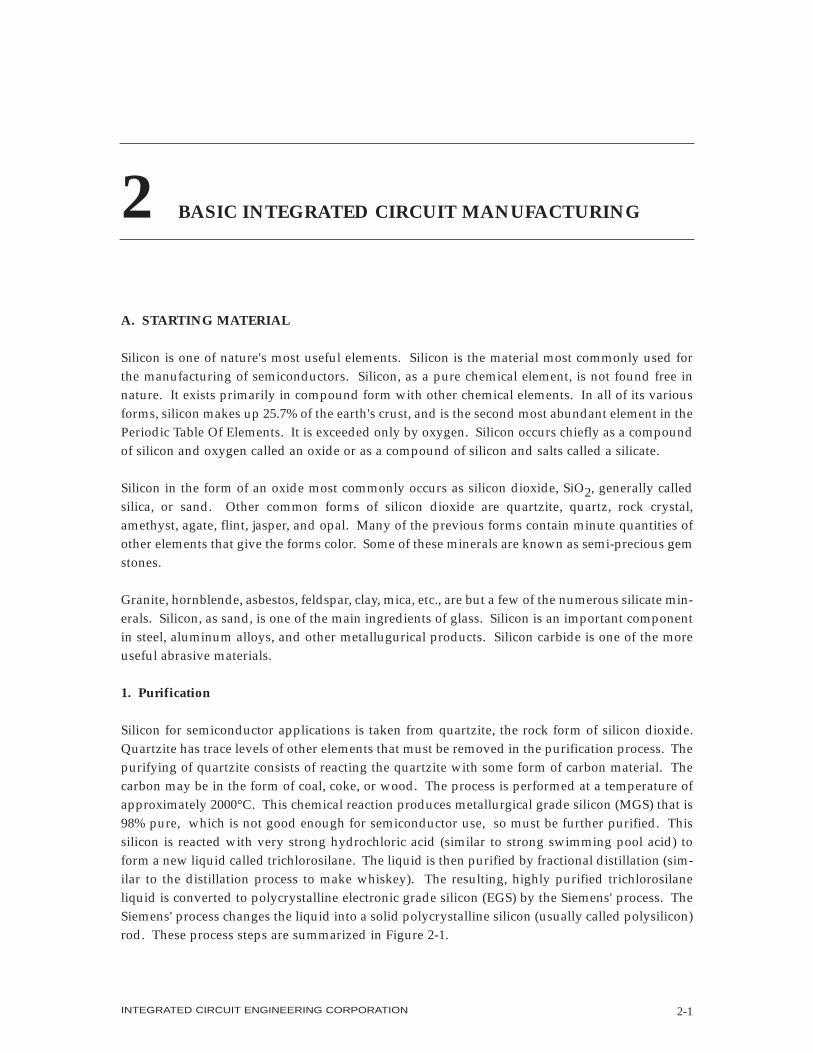
Silicon for semiconductor applications is taken from quartzite, the rock form of silicon dioxide.Quartzite has trace levels of other elements that must be removed in the purification process. Thepurifying of quartzite consists of reacting the quartzite with some form of carbon material. Thecarbon may be in the form of coal, coke, or wood. The process is performed at a temperature ofapproximately 2000°C. This chemical reaction produces metallurgical grade silicon (MGS) that is98% pure, which is not good enough for semiconductor use, so must be further purified. Thissilicon is reacted with very strong hydrochloric acid (similar to strong swimming pool acid) toform a new liquid called trichlorosilane. The liquid is then purified by fractional distillation (sim-ilar to the distillation process to make whiskey). The resulting, highly purified trichlorosilaneliquid is converted to polycrystalline electronic grade silicon (EGS) by the Siemens' process. TheSiemens' process changes the liquid into a solid polycrystalline silicon (usually called polysilicon)rod. These process steps are summarized in Figure 2-1.
INTEGRATED CIRCUIT ENGINEERING CORPORATION 2-1
2 BASIC INTEGRATED CIRCUIT MANUFACTURING
2. Czochralski Crystal Growing
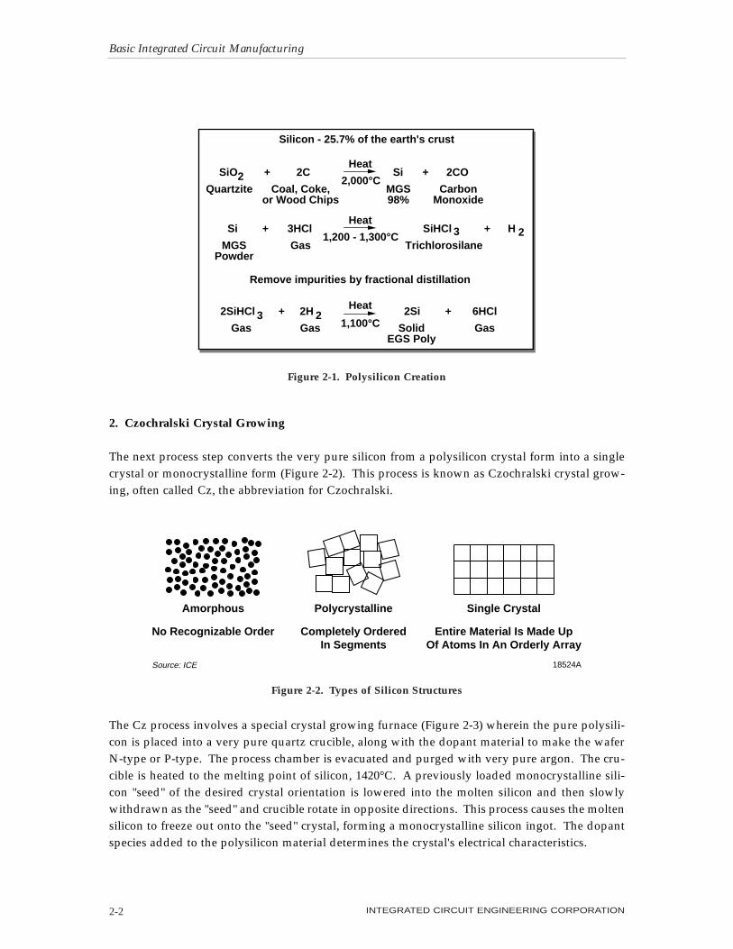
The next process step converts the very pure silicon from a polysilicon crystal form into a singlecrystal or monocrystalline form (Figure 2-2). This process is known as Czochralski crystal grow-ing, often called Cz, the abbreviation for Czochralski.
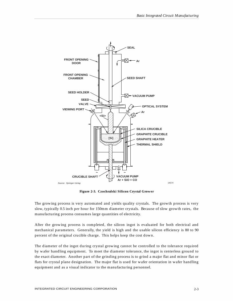
The Cz process involves a special crystal growing furnace (Figure 2-3) wherein the pure polysili-con is placed into a very pure quartz crucible, along with the dopant material to make the waferN-type or P-type. The process chamber is evacuated and purged with very pure argon. The cru-cible is heated to the melting point of silicon, 1420°C. A previously loaded monocrystalline sili-con "seed" of the desired crystal orientation is lowered into the molten silicon and then slowlywithdrawn as the "seed" and crucible rotate in opposite directions. This process causes the moltensilicon to freeze out onto the "seed" crystal, forming a monocrystalline silicon ingot. The dopantspecies added to the polysilicon material determines the crystal's electrical characteristics.
Basic Integrated Circuit Manufacturing
INTEGRATED CIRCUIT ENGINEERING CORPORATION2-2
Silicon - 25.7% of the earth's crust
2C 2CO
Quartzite2SiO +
Coal, Coke,or Wood Chips
Si
MGS98%
+
CarbonMonoxide
Heat
2,000°C
Heat
1,200 - 1,300°C3HCl
Gas
+Si
MGSPowder
SiHCl 3Trichlorosilane
+ H 2
Remove impurities by fractional distillation
2H 2Gas
+2SiHCl 3Gas
2Si
SolidEGS Poly
+ 6HCl
Gas1,100°C
Heat
Figure 2-1. Polysilicon Creation
Amorphous Polycrystalline Single Crystal
18524ASource: ICE
No Recognizable Order Completely OrderedIn Segments
Entire Material Is Made UpOf Atoms In An Orderly Array
Figure 2-2. Types of Silicon Structures
The growing process is very automated and yields quality crystals. The growth process is veryslow, typically 0.5 inch per hour for 150mm diameter crystals. Because of slow growth rates, themanufacturing process consumes large quantities of electricity.
After the growing process is completed, the silicon ingot is evaluated for both electrical andmechanical parameters. Generally, the yield is high and the usable silicon efficiency is 80 to 90percent of the original crucible charge. This helps keep the cost down.
The diameter of the ingot during crystal growing cannot be controlled to the tolerance requiredby wafer handling equipment. To meet the diameter tolerance, the ingot is centerless ground tothe exact diameter. Another part of the grinding process is to grind a major flat and minor flat orflats for crystal plane designation. The major flat is used for wafer orientation in wafer handlingequipment and as a visual indicator to the manufacturing personnel.
Basic Integrated Circuit Manufacturing
INTEGRATED CIRCUIT ENGINEERING CORPORATION 2-3
FRONT OPENINGDOOR
FRONT OPENINGCHAMBER SEED SHAFT
VACUUM PUMP
OPTICAL SYSTEM
Ar
SILICA CRUCIBLE
GRAPHITE CRUCIBLE
GRAPHITE HEATER
THERMAL SHIELD
VACUUM PUMPAr + SiO + CO
CRUCIBLE SHAFT
VIEWING PORT
VALVE
SEED
SEED HOLDER
Ar
SEAL
<Si>
[Si]
14574Source: Springer-Verlag
~ ~
Figure 2-3. Czochralski Silicon Crystal Grower
3. Sawing Crystal Into Wafers
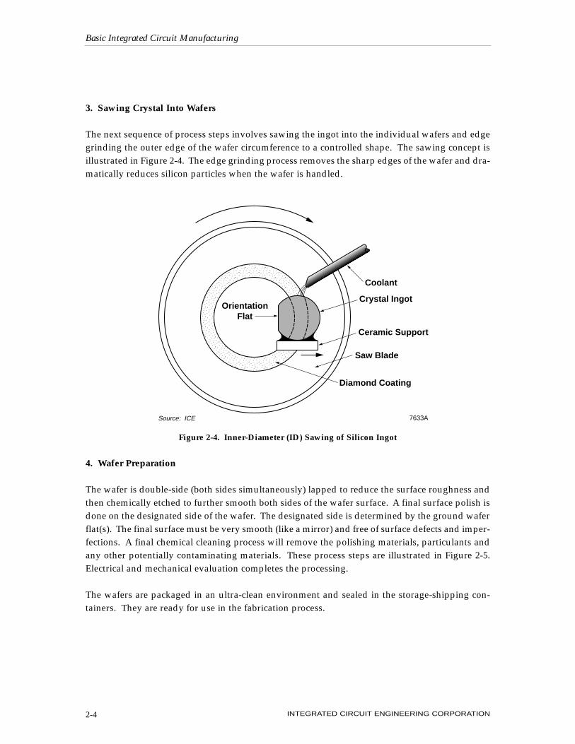
The next sequence of process steps involves sawing the ingot into the individual wafers and edgegrinding the outer edge of the wafer circumference to a controlled shape. The sawing concept isillustrated in Figure 2-4. The edge grinding process removes the sharp edges of the wafer and dra-matically reduces silicon particles when the wafer is handled.
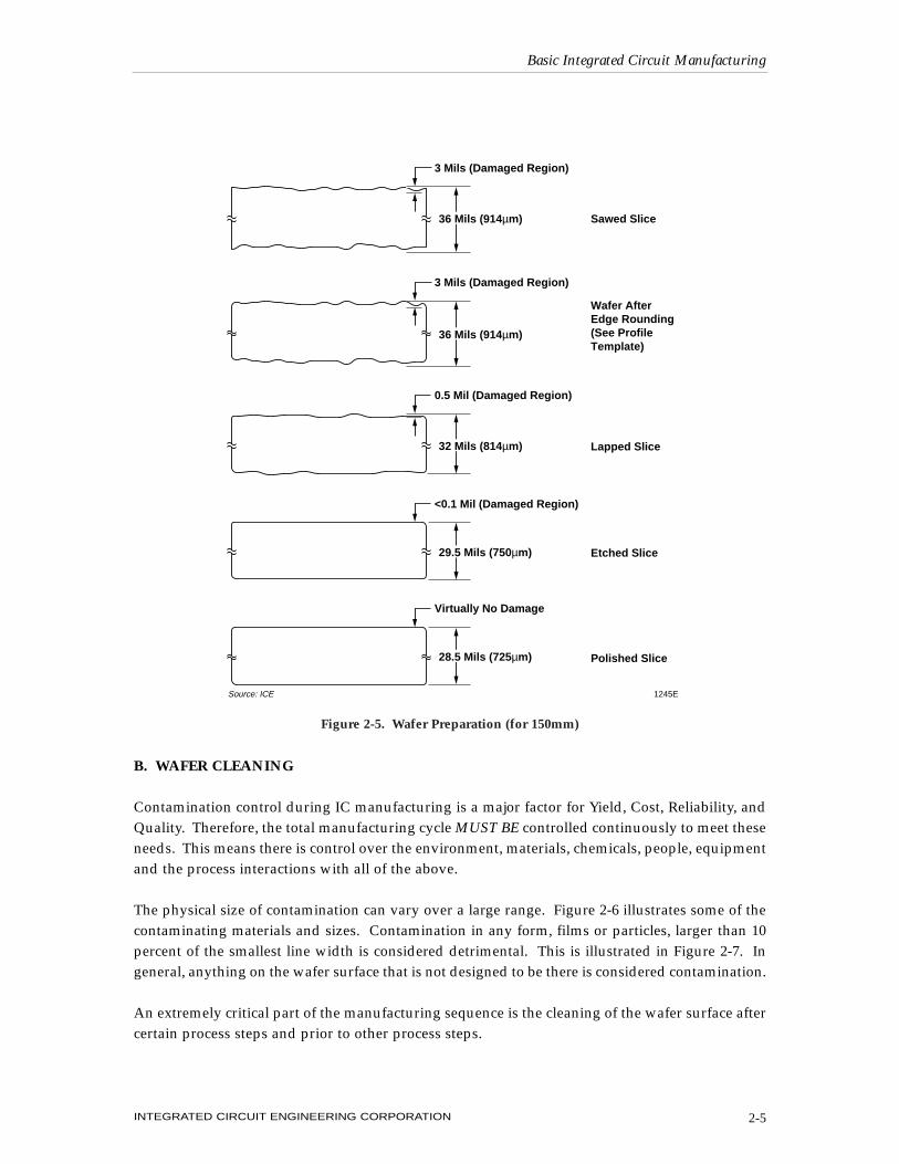
4. Wafer Preparation
The wafer is double-side (both sides simultaneously) lapped to reduce the surface roughness andthen chemically etched to further smooth both sides of the wafer surface. A final surface polish isdone on the designated side of the wafer. The designated side is determined by the ground waferflat(s). The final surface must be very smooth (like a mirror) and free of surface defects and imper-fections. A final chemical cleaning process will remove the polishing materials, particulants andany other potentially contaminating materials. These process steps are illustrated in Figure 2-5.Electrical and mechanical evaluation completes the processing.
The wafers are packaged in an ultra-clean environment and sealed in the storage-shipping con-tainers. They are ready for use in the fabrication process.
Basic Integrated Circuit Manufacturing
INTEGRATED CIRCUIT ENGINEERING CORPORATION2-4
OrientationFlat
Coolant
Crystal Ingot
Ceramic Support
Diamond Coating
Saw Blade
7633ASource: ICE
Figure 2-4. Inner-Diameter (ID) Sawing of Silicon Ingot
B. WAFER CLEANING
Contamination control during IC manufacturing is a major factor for Yield, Cost, Reliability, andQuality. Therefore, the total manufacturing cycle MUST BE controlled continuously to meet theseneeds. This means there is control over the environment, materials, chemicals, people, equipmentand the process interactions with all of the above.
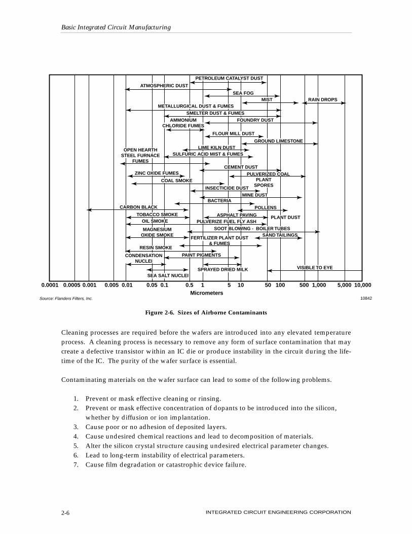
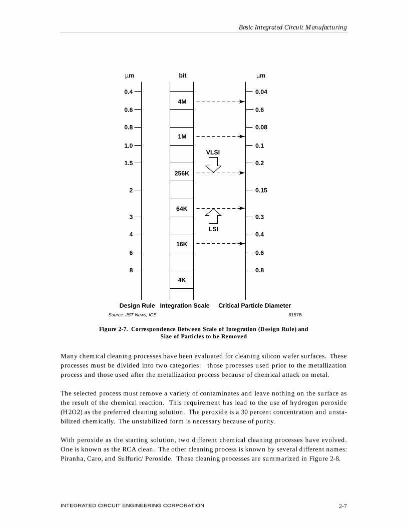
The physical size of contamination can vary over a large range. Figure 2-6 illustrates some of thecontaminating materials and sizes. Contamination in any form, films or particles, larger than 10percent of the smallest line width is considered detrimental. This is illustrated in Figure 2-7. Ingeneral, anything on the wafer surface that is not designed to be there is considered contamination.
An extremely critical part of the manufacturing sequence is the cleaning of the wafer surface aftercertain process steps and prior to other process steps.
Basic Integrated Circuit Manufacturing
INTEGRATED CIRCUIT ENGINEERING CORPORATION 2-5
3 Mils (Damaged Region)
36 Mils (914µm)
3 Mils (Damaged Region)
36 Mils (914µm)
0.5 Mil (Damaged Region)
32 Mils (814µm)
<0.1 Mil (Damaged Region)
29.5 Mils (750µm)
Virtually No Damage
28.5 Mils (725µm)
Sawed Slice
Wafer AfterEdge Rounding(See ProfileTemplate)
Lapped Slice
Etched Slice
Polished Slice
1245ESource: ICE
Figure 2-5. Wafer Preparation (for 150mm)
Cleaning processes are required before the wafers are introduced into any elevated temperatureprocess. A cleaning process is necessary to remove any form of surface contamination that maycreate a defective transistor within an IC die or produce instability in the circuit during the life-time of the IC. The purity of the wafer surface is essential.
Contaminating materials on the wafer surface can lead to some of the following problems.
1. Prevent or mask effective cleaning or rinsing.2. Prevent or mask effective concentration of dopants to be introduced into the silicon,
whether by diffusion or ion implantation.3. Cause poor or no adhesion of deposited layers.4. Cause undesired chemical reactions and lead to decomposition of materials.5. Alter the silicon crystal structure causing undesired electrical parameter changes.6. Lead to long-term instability of electrical parameters.7. Cause film degradation or catastrophic device failure.
Basic Integrated Circuit Manufacturing
INTEGRATED CIRCUIT ENGINEERING CORPORATION2-6
0.0001 0.0005 0.001 0.005 0.01 0.5 1 5 10 50 100 500 1,000 5,000 10,0000.05 0.1Micrometers
10842Source: Flanders Filters, Inc.
PETROLEUM CATALYST DUST
ATMOSPHERIC DUST
SEA FOGMIST RAIN DROPS
METALLURGICAL DUST & FUMES
SMELTER DUST & FUMES
AMMONIUMCHLORIDE FUMES
FOUNDRY DUST
FLOUR MILL DUST
GROUND LIMESTONELIME KILN DUSTOPEN HEARTH
STEEL FURNACEFUMES
SULFURIC ACID MIST & FUMES
CEMENT DUSTZINC OXIDE FUMES PULVERIZED COAL
COAL SMOKE PLANTSPORES
INSECTICIDE DUST
MINE DUSTBACTERIA
CARBON BLACK POLLENS
TOBACCO SMOKE ASPHALT PAVING PLANT DUSTOIL SMOKE PULVERIZE FUEL FLY ASH
MAGNESIUMOXIDE SMOKE
SOOT BLOWING - BOILER TUBES
FERTILIZER PLANT DUST& FUMES
SAND TAILINGS
RESIN SMOKE
CONDENSATIONNUCLEI
PAINT PIGMENTS
SEA SALT NUCLEISPRAYED DRIED MILK VISIBLE TO EYE
Figure 2-6. Sizes of Airborne Contaminants
Many chemical cleaning processes have been evaluated for cleaning silicon wafer surfaces. Theseprocesses must be divided into two categories: those processes used prior to the metallizationprocess and those used after the metallization process because of chemical attack on metal.
The selected process must remove a variety of contaminates and leave nothing on the surface asthe result of the chemical reaction. This requirement has lead to the use of hydrogen peroxide(H2O2) as the preferred cleaning solution. The peroxide is a 30 percent concentration and unsta-bilized chemically. The unstabilized form is necessary because of purity.
With peroxide as the starting solution, two different chemical cleaning processes have evolved.One is known as the RCA clean. The other cleaning process is known by several different names:Piranha, Caro, and Sulfuric/Peroxide. These cleaning processes are summarized in Figure 2-8.
Basic Integrated Circuit Manufacturing
INTEGRATED CIRCUIT ENGINEERING CORPORATION 2-7
0.4
0.6
0.8
1.0
1.5
2
3
4
6
8
0.04
0.6
0.08
0.1
0.2
0.15
0.3
0.4
0.6
0.8
4M
1M
256K
64K
16K
4K
µm µmbit
Critical Particle DiameterIntegration ScaleDesign Rule8157BSource: JST News, ICE
VLSI
LSI
Figure 2-7. Correspondence Between Scale of Integration (Design Rule) andSize of Particles to be Removed
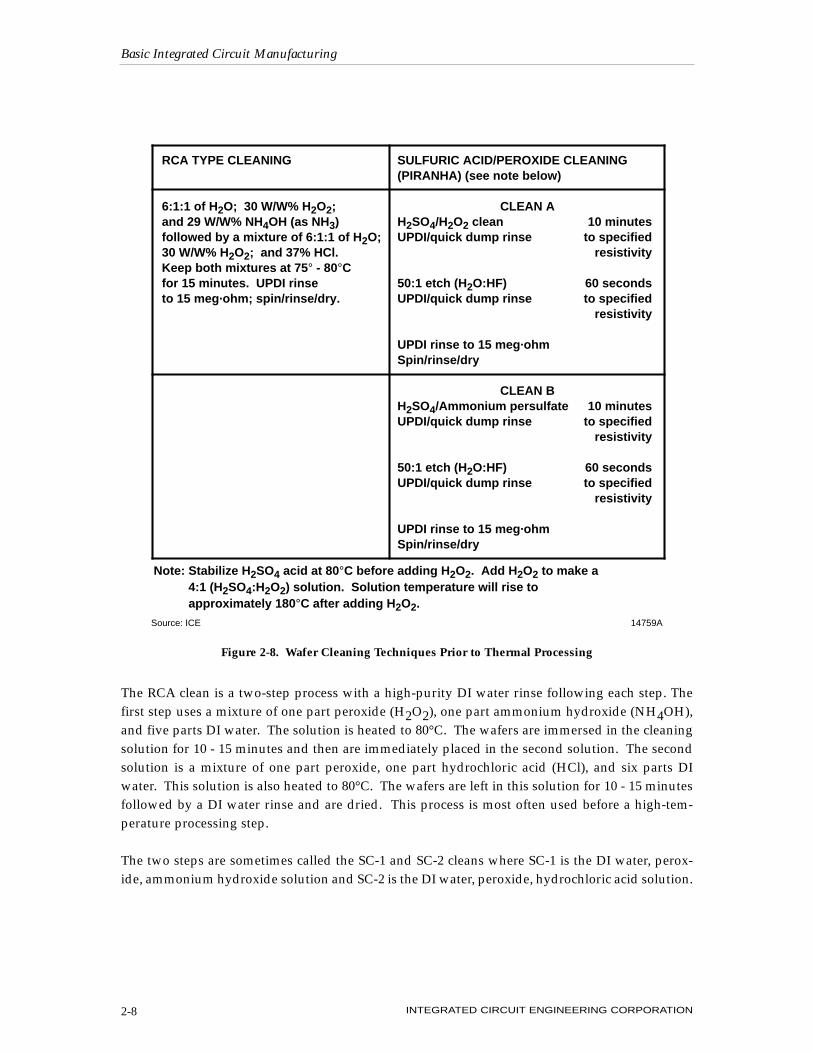
The RCA clean is a two-step process with a high-purity DI water rinse following each step. Thefirst step uses a mixture of one part peroxide (H2O2), one part ammonium hydroxide (NH4OH),and five parts DI water. The solution is heated to 80°C. The wafers are immersed in the cleaningsolution for 10 - 15 minutes and then are immediately placed in the second solution. The secondsolution is a mixture of one part peroxide, one part hydrochloric acid (HCl), and six parts DIwater. This solution is also heated to 80°C. The wafers are left in this solution for 10 - 15 minutesfollowed by a DI water rinse and are dried. This process is most often used before a high-tem-perature processing step.
The two steps are sometimes called the SC-1 and SC-2 cleans where SC-1 is the DI water, perox-ide, ammonium hydroxide solution and SC-2 is the DI water, peroxide, hydrochloric acid solution.
Basic Integrated Circuit Manufacturing
INTEGRATED CIRCUIT ENGINEERING CORPORATION2-8
RCA TYPE CLEANING
6:1:1 of H2O; 30 W/W% H2O2;and 29 W/W% NH4OH (as NH3) followed by a mixture of 6:1:1 of H2O; 30 W/W% H2O2; and 37% HCl.Keep both mixtures at 75° - 80°C for 15 minutes. UPDI rinseto 15 meg·ohm; spin/rinse/dry.
SULFURIC ACID/PEROXIDE CLEANING (PIRANHA) (see note below)
CLEAN AH2SO4/H2O2 clean 10 minutesUPDI/quick dump rinse to specified
resistivity
50:1 etch (H2O:HF) 60 secondsUPDI/quick dump rinse to specified
resistivity
UPDI rinse to 15 meg·ohmSpin/rinse/dry
CLEAN BH2SO4/Ammonium persulfate 10 minutesUPDI/quick dump rinse to specified
resistivity
50:1 etch (H2O:HF) 60 secondsUPDI/quick dump rinse to specified
resistivity
UPDI rinse to 15 meg·ohmSpin/rinse/dry
Note: Stabilize H2SO4 acid at 80°C before adding H2O2. Add H2O2 to make a 4:1 (H2SO4:H2O2) solution. Solution temperature will rise toapproximately 180°C after adding H2O2.
14759ASource: ICE
Figure 2-8. Wafer Cleaning Techniques Prior to Thermal Processing
The sulfuric acid and hydrogen peroxide solution, often written as H2SO4-H2O2, is most oftenused to strip photoresist from the wafer surface.
The sulfuric acid-hydrogen peroxide solution is formulated by heating the sulfuric acid to 80 -100°C and adding the peroxide just prior to the wafer cleaning step. The solution contains threeto five volumes of sulfuric acid to one volume of peroxide. Since both sulfuric acid and hydrogenperoxide are strong oxidizing agents, mixing them together causes an exothermic chemical reac-tion (liberates heat) raising the solution temperature to 150 - 180°C, depending on the chemicalratios. This sudden increase in temperature aids in the chemical cleaning process. The wafers areimmersed in the solution for 10 - 15 minutes followed by a DI water rinse and are dried.
C. DIELECTRIC FORMATION
A dielectric is a material that is a poor conductor of electricity or does not conduct at all. Dielectriclayers are often called insulators. Dielectric layers play a critical role in the manufacturing andoperation of semiconductors. They are used:
• for insulation between conducting layers (e.g., for devices with more than one level ofmetal and to separate the gate from the silicon in an MOS transistor),
• to protect the surface of a completed die,
• to mask off portions of the surface of the wafer during some manufacturing operations, and
• between the plates of capacitors in ICs.
Various forms of dielectrics related to semiconductors include silicon dioxide, silicon nitride, andsilicon oxynitride. The most common is silicon dioxide.
1. Thermally Grown Silicon Dioxide
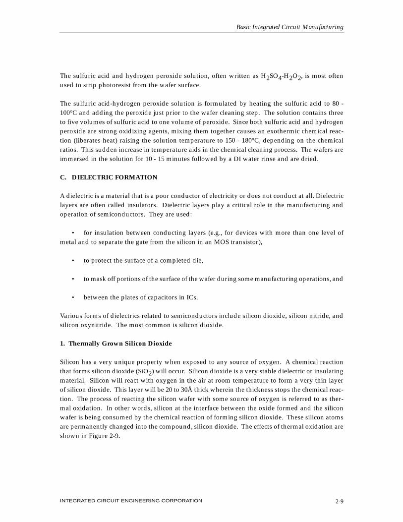
Silicon has a very unique property when exposed to any source of oxygen. A chemical reactionthat forms silicon dioxide (SiO2) will occur. Silicon dioxide is a very stable dielectric or insulatingmaterial. Silicon will react with oxygen in the air at room temperature to form a very thin layerof silicon dioxide. This layer will be 20 to 30Å thick wherein the thickness stops the chemical reac-tion. The process of reacting the silicon wafer with some source of oxygen is referred to as ther-mal oxidation. In other words, silicon at the interface between the oxide formed and the siliconwafer is being consumed by the chemical reaction of forming silicon dioxide. These silicon atomsare permanently changed into the compound, silicon dioxide. The effects of thermal oxidation areshown in Figure 2-9.
Basic Integrated Circuit Manufacturing
INTEGRATED CIRCUIT ENGINEERING CORPORATION 2-9
a. Atmospheric-Pressure Oxidation
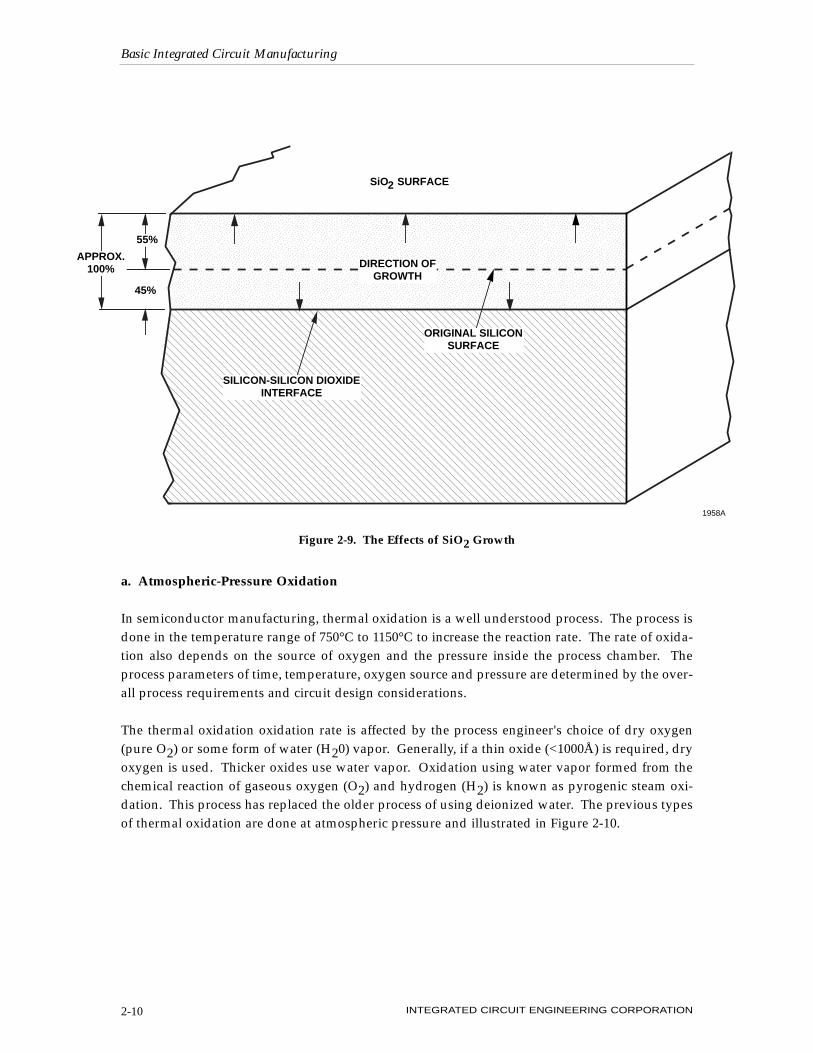
In semiconductor manufacturing, thermal oxidation is a well understood process. The process isdone in the temperature range of 750°C to 1150°C to increase the reaction rate. The rate of oxida-tion also depends on the source of oxygen and the pressure inside the process chamber. Theprocess parameters of time, temperature, oxygen source and pressure are determined by the over-all process requirements and circuit design considerations.
The thermal oxidation oxidation rate is affected by the process engineer's choice of dry oxygen(pure O2) or some form of water (H20) vapor. Generally, if a thin oxide (<1000Å) is required, dryoxygen is used. Thicker oxides use water vapor. Oxidation using water vapor formed from thechemical reaction of gaseous oxygen (O2) and hydrogen (H2) is known as pyrogenic steam oxi-dation. This process has replaced the older process of using deionized water. The previous typesof thermal oxidation are done at atmospheric pressure and illustrated in Figure 2-10.
Basic Integrated Circuit Manufacturing
INTEGRATED CIRCUIT ENGINEERING CORPORATION2-10
45%
SiO SURFACE2
SILICON-SILICON DIOXIDEINTERFACE
ORIGINAL SILICONSURFACE
DIRECTION OFGROWTH
APPROX.100%
55%
1958A
Figure 2-9. The Effects of SiO2 Growth
b. High-Pressure Oxidation
As feature sizes of integrated circuits continue to decrease further into the submicron size, moreshallow junctions are required and process temperatures are therefore being forced to lowerlevels. This has brought about a renewed use of high-pressure oxidation systems. These systemsoriginated in about 1970, but have been slow to evolve into manufacturing.
Basic Integrated Circuit Manufacturing
INTEGRATED CIRCUIT ENGINEERING CORPORATION 2-11
Quartz Oxidation Boat and Silicon Wafers
Exhaust
Furnace
Furnace
Furnace
O2N2HClor TCA
O2N2HClor TCA
O2N2 H2HClor TCA
C. Pyrogenic Steam Oxidation
B. Wet Oxygen Oxidation
A. Dry O2 Oxidation
110V
TemperatureController
Safety Vent
DlH2O
HeatingMantle
1142BSource: ICE
Figure 2-10. Oxidation Systems
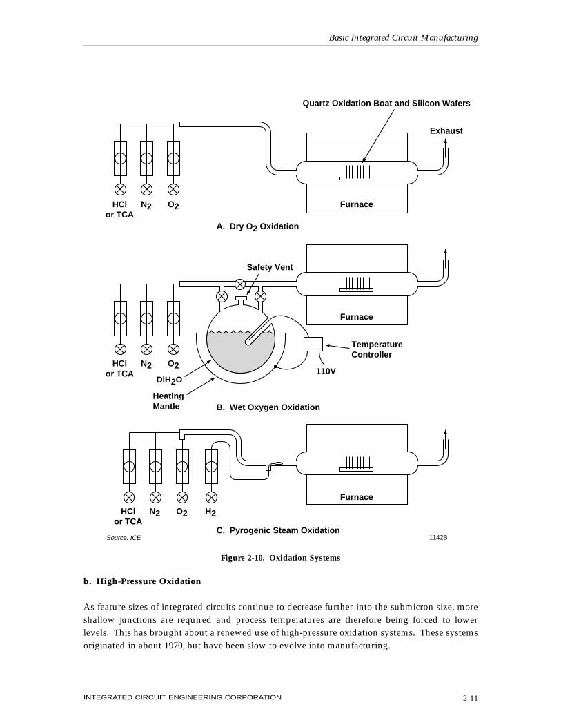
The process chamber on this system is fitted with a High-Pressure Vessel. This allows the systemto be pressurized from one to twenty-five (25) atmospheres (14.7 psi to 367.5 psi). This allows theprocess engineer to lower temperature by raising the pressure of the process chamber and hasallowed some new degrees of process choices. In addition, this equipment has shown a reductionin oxidation defects when compared to the atmospheric-pressure process.
The disadvantages of high-pressure oxidation are the higher cost of the equipment, the equipmentuses twice the floor space, and the safety considerations are stringent.
The advantages today more than offset the disadvantages because of the need for lower temper-ature processing.
2. CVD Silicon Dioxide
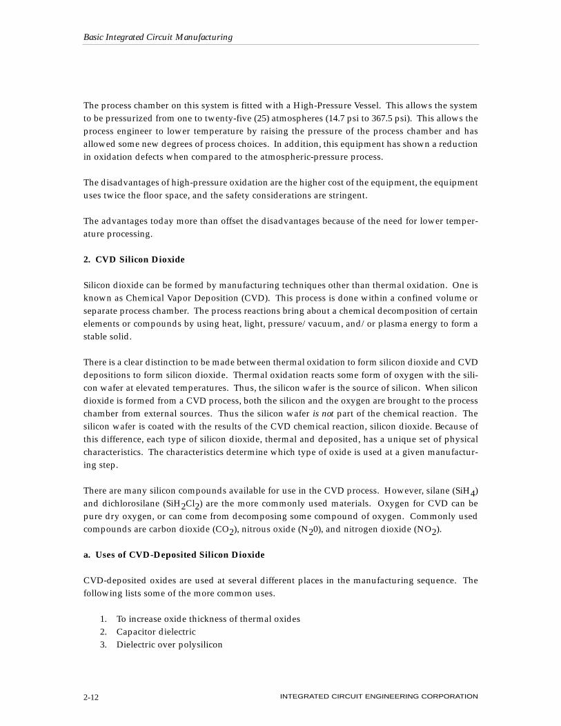
Silicon dioxide can be formed by manufacturing techniques other than thermal oxidation. One isknown as Chemical Vapor Deposition (CVD). This process is done within a confined volume orseparate process chamber. The process reactions bring about a chemical decomposition of certainelements or compounds by using heat, light, pressure/vacuum, and/or plasma energy to form astable solid.
There is a clear distinction to be made between thermal oxidation to form silicon dioxide and CVDdepositions to form silicon dioxide. Thermal oxidation reacts some form of oxygen with the sili-con wafer at elevated temperatures. Thus, the silicon wafer is the source of silicon. When silicondioxide is formed from a CVD process, both the silicon and the oxygen are brought to the processchamber from external sources. Thus the silicon wafer is not part of the chemical reaction. Thesilicon wafer is coated with the results of the CVD chemical reaction, silicon dioxide. Because ofthis difference, each type of silicon dioxide, thermal and deposited, has a unique set of physicalcharacteristics. The characteristics determine which type of oxide is used at a given manufactur-ing step.
There are many silicon compounds available for use in the CVD process. However, silane (SiH4)and dichlorosilane (SiH2Cl2) are the more commonly used materials. Oxygen for CVD can bepure dry oxygen, or can come from decomposing some compound of oxygen. Commonly usedcompounds are carbon dioxide (CO2), nitrous oxide (N20), and nitrogen dioxide (NO2).
a. Uses of CVD-Deposited Silicon Dioxide
CVD-deposited oxides are used at several different places in the manufacturing sequence. Thefollowing lists some of the more common uses.
1. To increase oxide thickness of thermal oxides2. Capacitor dielectric3. Dielectric over polysilicon
Basic Integrated Circuit Manufacturing
INTEGRATED CIRCUIT ENGINEERING CORPORATION2-12
4. Dielectric over metal5. Buffer oxide layer to match mechanical requirements6. Masking oxide layer7. Final passivation
Deposited oxide is not normally used as a gate oxide for MOS transistors. Gate oxide is formedby some thermal oxidation technique.
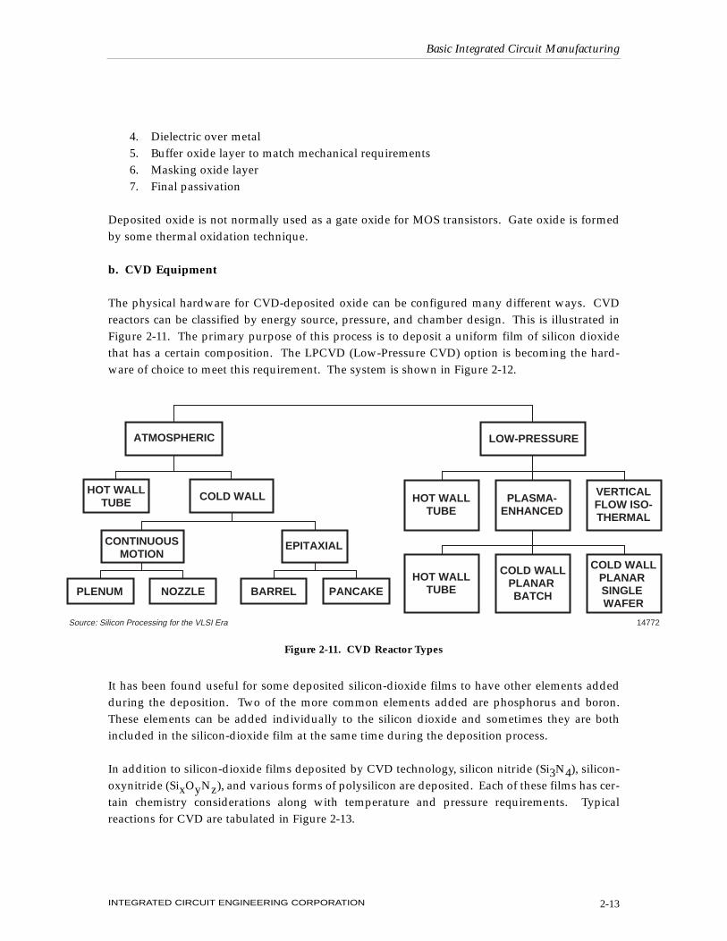
b. CVD Equipment
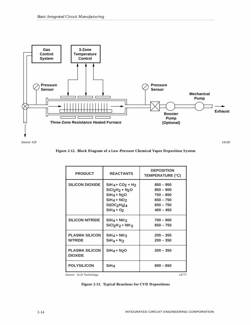
The physical hardware for CVD-deposited oxide can be configured many different ways. CVDreactors can be classified by energy source, pressure, and chamber design. This is illustrated inFigure 2-11. The primary purpose of this process is to deposit a uniform film of silicon dioxidethat has a certain composition. The LPCVD (Low-Pressure CVD) option is becoming the hard-ware of choice to meet this requirement. The system is shown in Figure 2-12.
It has been found useful for some deposited silicon-dioxide films to have other elements addedduring the deposition. Two of the more common elements added are phosphorus and boron.These elements can be added individually to the silicon dioxide and sometimes they are bothincluded in the silicon-dioxide film at the same time during the deposition process.
In addition to silicon-dioxide films deposited by CVD technology, silicon nitride (Si3N4), silicon-oxynitride (SixOyNz), and various forms of polysilicon are deposited. Each of these films has cer-tain chemistry considerations along with temperature and pressure requirements. Typicalreactions for CVD are tabulated in Figure 2-13.
Basic Integrated Circuit Manufacturing
INTEGRATED CIRCUIT ENGINEERING CORPORATION 2-13
ATMOSPHERIC
HOT WALLTUBE COLD WALL
CONTINUOUSMOTION
PLENUM NOZZLE
EPITAXIAL
BARREL PANCAKE
HOT WALLTUBE
PLASMA-ENHANCED
VERTICALFLOW ISO-THERMAL
HOT WALLTUBE
COLD WALLPLANAR BATCH
COLD WALLPLANAR SINGLE WAFER
LOW-PRESSURE
14772Source: Silicon Processing for the VLSI Era
Figure 2-11. CVD Reactor Types
Basic Integrated Circuit Manufacturing
INTEGRATED CIRCUIT ENGINEERING CORPORATION2-14
GasControlSystem
3-ZoneTemperature
Control
PressureSensor
PressureSensor
Three-Zone Resistance Heated Furnace
BoosterPump
(Optional)
MechanicalPump
Exhaust
1313DSource: ICE
Figure 2-12. Block Diagram of a Low-Pressure Chemical Vapor Deposition System
SiH + CO + H SiCl H + N OSiH + N OSiH + NOSi(OC H )SiH + O
SiH + NHSiCl H + NH
SiH + NHSiH + N
SiH + N O
SiH
4 22 2 24 24 2
2 5 44 2
4 332 2
4 34 2
4 2
4
PRODUCT REACTANTSDEPOSITION
TEMPERATURE (°C)
SILICON DIOXIDE
SILICON NITRIDE
PLASMA SILICONNITRIDE
PLASMA SILICONDIOXIDE
POLYSILICON
850 – 950850 – 900750 – 850650 – 750650 – 750400 – 450
700 – 900650 – 750
200 – 350200 – 350
200 – 350
600 – 650
2
14777Source: VLSI Technology
Figure 2-13. Typical Reactions for CVD Depositions
D. PHOTOLITHOGRAPHY
1. Overview
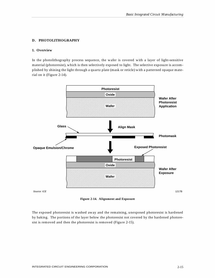
In the photolithography process sequence, the wafer is covered with a layer of light-sensitivematerial (photoresist), which is then selectively exposed to light. The selective exposure is accom-plished by shining the light through a quartz plate (mask or reticle) with a patterned opaque mate-rial on it (Figure 2-14).
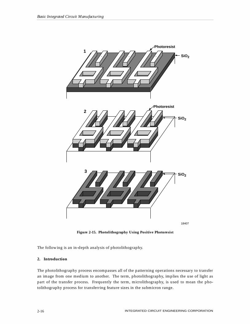
The exposed photoresist is washed away and the remaining, unexposed photoresist is hardenedby baking. The portions of the layer below the photoresist not covered by the hardened photore-sist is removed and then the photoresist is removed (Figure 2-15).
Basic Integrated Circuit Manufacturing
INTEGRATED CIRCUIT ENGINEERING CORPORATION 2-15
Align Mask
Photoresist
Oxide
Wafer
1217BSource: ICE
Wafer AfterExposure
Photoresist
Oxide
Wafer
Wafer AfterPhotoresistApplication
Exposed Photoresist
Glass
Opaque Emulsion/Chrome
Photomask
Figure 2-14. Alignment and Exposure
The following is an in-depth analysis of photolithography.
2. Introduction
The photolithography process encompasses all of the patterning operations necessary to transferan image from one medium to another. The term, photolithography, implies the use of light aspart of the transfer process. Frequently the term, microlithography, is used to mean the pho-tolithography process for transferring feature sizes in the submicron range.
Basic Integrated Circuit Manufacturing
INTEGRATED CIRCUIT ENGINEERING CORPORATION2-16
Photoresist
SiO2
18407
Photoresist
SiO2
SiO2
1
2
3
Figure 2-15. Photolithography Using Positive Photoresist
The photolithography process involves the transfer of geometric images created by a circuitdesigner to a photosensitive film applied to the surface of the silicon wafer. The sized geometri-cal features are the physical designs of the various circuit elements, i.e., transistors, resistors,capacitors, etc., that will make up the electrical circuit design.
Since the early 1970's the concept of making the physical size of the transistor smaller to increasethe transistor performance has been the evolutionary force behind the semiconductor industry.This has placed a constant pressure on the photolithography process to print smaller feature sizes.
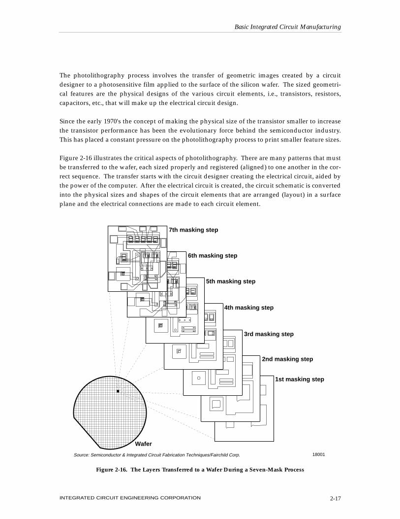
Figure 2-16 illustrates the critical aspects of photolithography. There are many patterns that mustbe transferred to the wafer, each sized properly and registered (aligned) to one another in the cor-rect sequence. The transfer starts with the circuit designer creating the electrical circuit, aided bythe power of the computer. After the electrical circuit is created, the circuit schematic is convertedinto the physical sizes and shapes of the circuit elements that are arranged (layout) in a surfaceplane and the electrical connections are made to each circuit element.
Basic Integrated Circuit Manufacturing
INTEGRATED CIRCUIT ENGINEERING CORPORATION 2-17
7th masking step
6th masking step
5th masking step
4th masking step
2nd masking step
1st masking step
Wafer
Source: Semiconductor & Integrated Circuit Fabrication Techniques/Fairchild Corp. 18001
3rd masking step
Figure 2-16. The Layers Transferred to a Wafer During a Seven-Mask Process
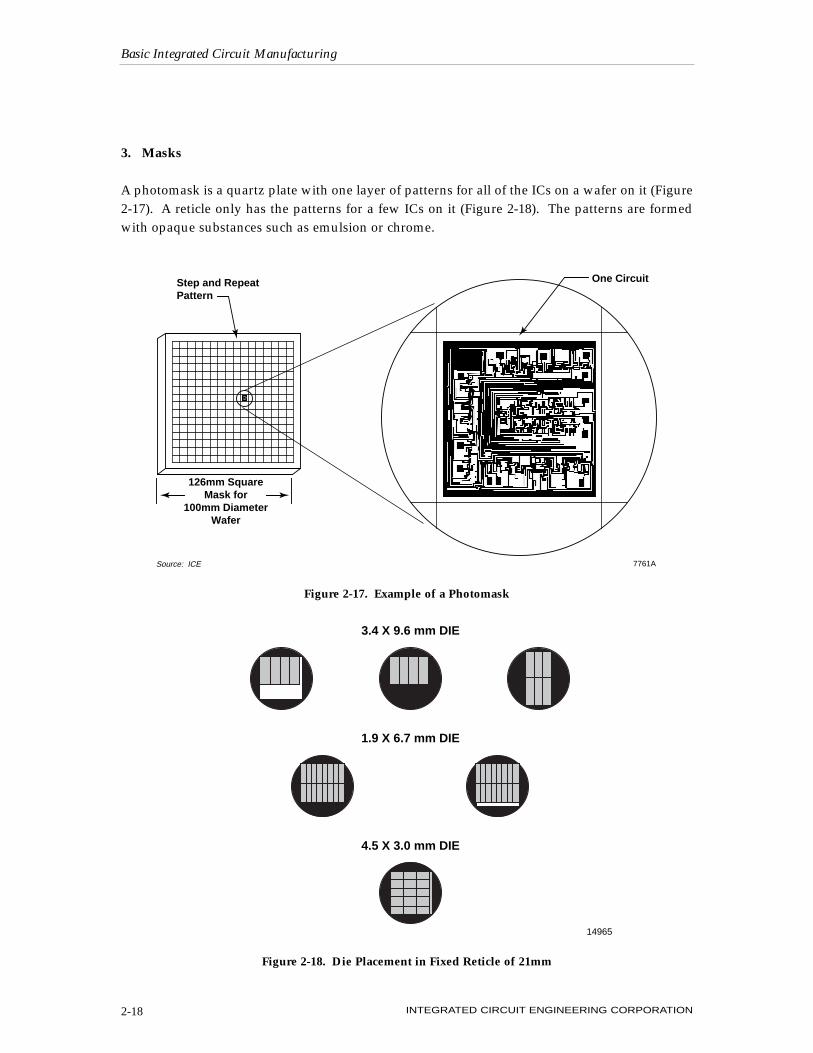
3. Masks
A photomask is a quartz plate with one layer of patterns for all of the ICs on a wafer on it (Figure2-17). A reticle only has the patterns for a few ICs on it (Figure 2-18). The patterns are formedwith opaque substances such as emulsion or chrome.
Basic Integrated Circuit Manufacturing
INTEGRATED CIRCUIT ENGINEERING CORPORATION2-18
Step and RepeatPattern
7761ASource: ICE
126mm SquareMask for
100mm DiameterWafer
One Circuit
Figure 2-17. Example of a Photomask
3.4 X 9.6 mm DIE
1.9 X 6.7 mm DIE
4.5 X 3.0 mm DIE
14965
Figure 2-18. Die Placement in Fixed Reticle of 21mm
Emulsion images on the glass substrate are difficult to clean. Typically they are used for a limitednumber of exposures and then discarded. On the other hand, chrome images on the glass sub-strate can be cleaned, inspected, and reused many times.
a. Reticles
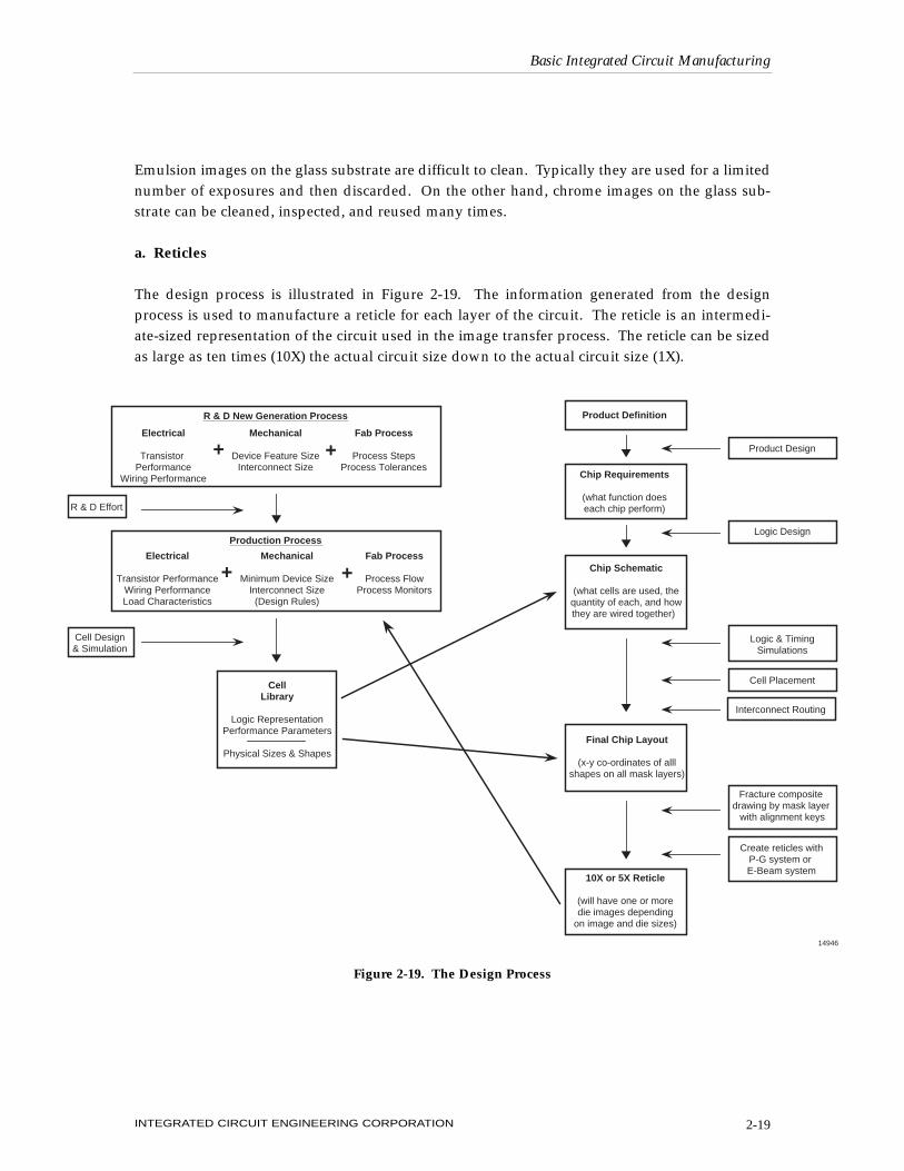
The design process is illustrated in Figure 2-19. The information generated from the designprocess is used to manufacture a reticle for each layer of the circuit. The reticle is an intermedi-ate-sized representation of the circuit used in the image transfer process. The reticle can be sizedas large as ten times (10X) the actual circuit size down to the actual circuit size (1X).
Basic Integrated Circuit Manufacturing
INTEGRATED CIRCUIT ENGINEERING CORPORATION 2-19
Product Definition
Chip Requirements
(what function doeseach chip perform)
Chip Schematic
(what cells are used, thequantity of each, and howthey are wired together)
Final Chip Layout
(x-y co-ordinates of alllshapes on all mask layers)
10X or 5X Reticle
(will have one or moredie images depending
on image and die sizes)
Logic Design
Product Design
Logic & TimingSimulations
Cell Placement
Interconnect Routing
Create reticles with P-G system or E-Beam system
Fracture composite drawing by mask layer
with alignment keys
R & D New Generation Process
Electrical
Transistor Performance
Wiring Performance
Mechanical
Device Feature SizeInterconnect Size
Fab Process
Process StepsProcess Tolerances
+ +
Production Process
Electrical
Transistor PerformanceWiring PerformanceLoad Characteristics
Mechanical
Minimum Device SizeInterconnect Size
(Design Rules)
Fab Process
Process FlowProcess Monitors
+ +
CellLibrary
Logic RepresentationPerformance Parameters
Physical Sizes & Shapes
Cell Design& Simulation
R & D Effort
14946
Figure 2-19. The Design Process
The manufacturing procedures and equipment used for reticle generation require the best preci-sion and reproducible imaging technology known. The quality of the reticle can impact the yieldsof the actual IC manufacturing.
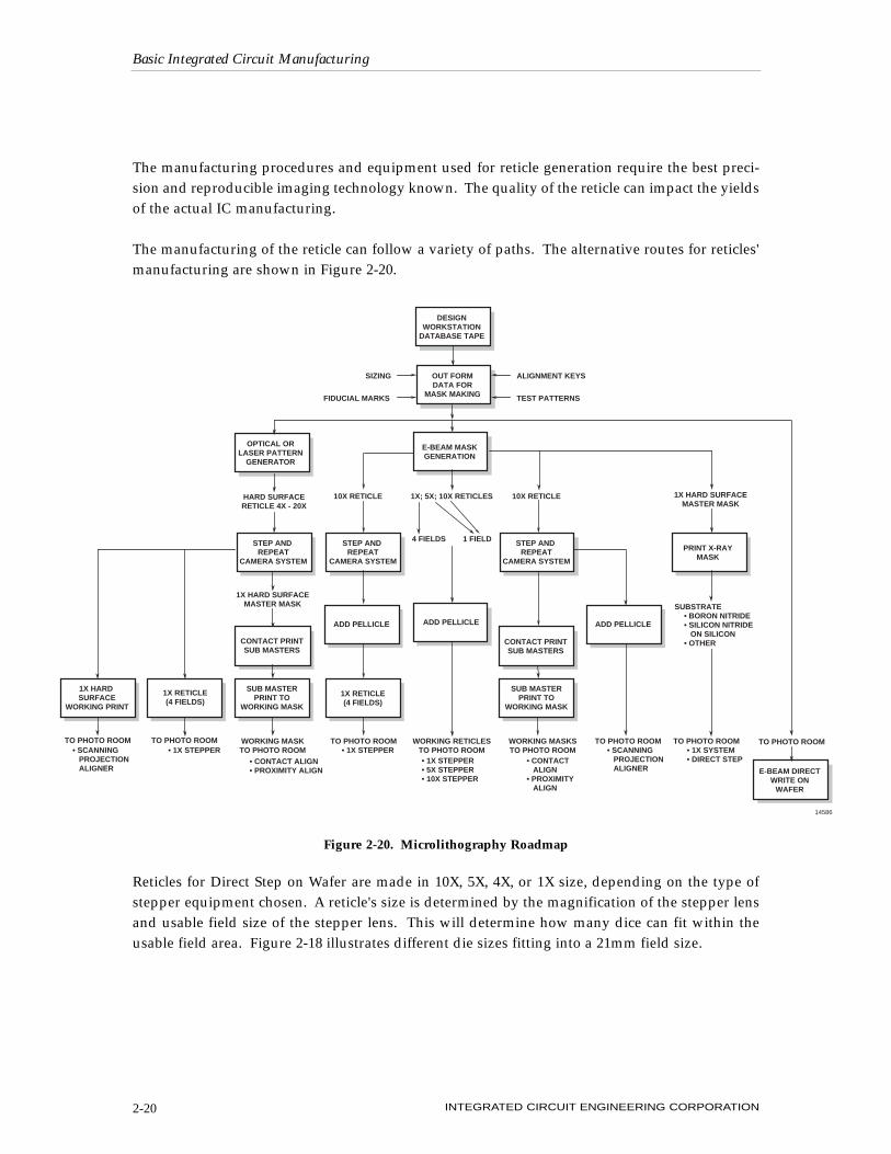
The manufacturing of the reticle can follow a variety of paths. The alternative routes for reticles'manufacturing are shown in Figure 2-20.
Reticles for Direct Step on Wafer are made in 10X, 5X, 4X, or 1X size, depending on the type ofstepper equipment chosen. A reticle's size is determined by the magnification of the stepper lensand usable field size of the stepper lens. This will determine how many dice can fit within theusable field area. Figure 2-18 illustrates different die sizes fitting into a 21mm field size.
Basic Integrated Circuit Manufacturing
INTEGRATED CIRCUIT ENGINEERING CORPORATION2-20
DESIGNWORKSTATION
DATABASE TAPE
OUT FORMDATA FOR
MASK MAKING
STEP AND REPEAT
CAMERA SYSTEM
ADD PELLICLE
SIZING
FIDUCIAL MARKS
ALIGNMENT KEYS
TEST PATTERNS
OPTICAL ORLASER PATTERN
GENERATOR
HARD SURFACERETICLE 4X - 20X
1X HARD SURFACEMASTER MASK
CONTACT PRINTSUB MASTERS
SUB MASTERPRINT TO
WORKING MASK
WORKING MASKTO PHOTO ROOM
• CONTACT ALIGN• PROXIMITY ALIGN
E-BEAM MASKGENERATION
1X; 5X; 10X RETICLES
4 FIELDS 1 FIELD
WORKING RETICLESTO PHOTO ROOM• 1X STEPPER• 5X STEPPER• 10X STEPPER
STEP AND REPEAT
CAMERA SYSTEM
CONTACT PRINTSUB MASTERS
SUB MASTERPRINT TO
WORKING MASK
WORKING MASKSTO PHOTO ROOM
• CONTACT ALIGN• PROXIMITY ALIGN
PRINT X-RAYMASK
1X HARD SURFACEMASTER MASK
SUBSTRATE• BORON NITRIDE• SILICON NITRIDE ON SILICON• OTHER
TO PHOTO ROOM• 1X SYSTEM• DIRECT STEP
14586
1X HARD SURFACE
WORKING PRINT
TO PHOTO ROOM• SCANNING PROJECTION ALIGNER
1X RETICLE(4 FIELDS)
TO PHOTO ROOM• 1X STEPPER
E-BEAM DIRECTWRITE ON
WAFER
TO PHOTO ROOM
STEP AND REPEAT
CAMERA SYSTEM
1X RETICLE(4 FIELDS)
TO PHOTO ROOM• 1X STEPPER
ADD PELLICLE
10X RETICLE 10X RETICLE
ADD PELLICLE
• SCANNING PROJECTION ALIGNER
TO PHOTO ROOM
Figure 2-20. Microlithography Roadmap
b. Photomasks
The photomask is created by a series of additional process steps beyond the making of a 10X ret-icle for each layer. Refer to Figure 2-20. At the contact print to submaster stage the mask polaritymust be determined (depends on whether negative or positive photoresist is used). The submas-ter to working print stage can print either emulsion or chrome on glass substrates. The choice isdetermined by the wafer alignment equipment. A photomask is shown in Figure 2-17.
c. E-beam
Also shown in Figure 2-20 are two other alternative technologies to form the designer's require-ments into a photoresist layer on the silicon wafer. One alternative is to use an e-beam system towrite the pattern directly on the photoresist-coated wafer. This approach eliminates the reticles ormask-making stage but has a very slow throughput.
d. X-ray
The other technique uses x-ray energy to expose the photoresist-coated wafer. The mask for thistechnique is very expensive and difficult to manufacture. However, x-ray steppers have excellentresolution capability and will probably be needed by the end of the 1990's.
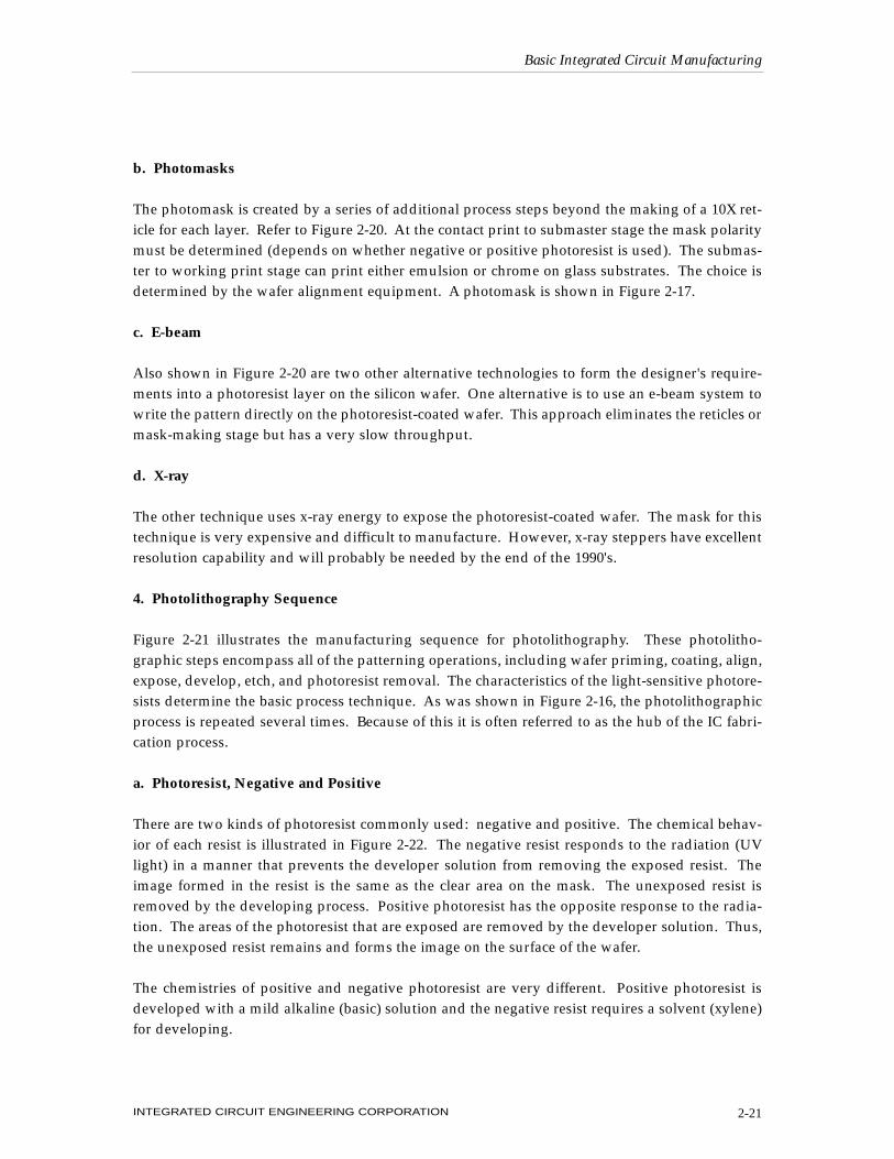
4. Photolithography Sequence
Figure 2-21 illustrates the manufacturing sequence for photolithography. These photolitho-graphic steps encompass all of the patterning operations, including wafer priming, coating, align,expose, develop, etch, and photoresist removal. The characteristics of the light-sensitive photore-sists determine the basic process technique. As was shown in Figure 2-16, the photolithographicprocess is repeated several times. Because of this it is often referred to as the hub of the IC fabri-cation process.
a. Photoresist, Negative and Positive
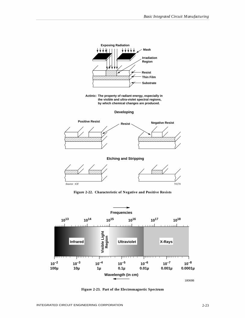
There are two kinds of photoresist commonly used: negative and positive. The chemical behav-ior of each resist is illustrated in Figure 2-22. The negative resist responds to the radiation (UVlight) in a manner that prevents the developer solution from removing the exposed resist. Theimage formed in the resist is the same as the clear area on the mask. The unexposed resist isremoved by the developing process. Positive photoresist has the opposite response to the radia-tion. The areas of the photoresist that are exposed are removed by the developer solution. Thus,the unexposed resist remains and forms the image on the surface of the wafer.
The chemistries of positive and negative photoresist are very different. Positive photoresist isdeveloped with a mild alkaline (basic) solution and the negative resist requires a solvent (xylene)for developing.
Basic Integrated Circuit Manufacturing
INTEGRATED CIRCUIT ENGINEERING CORPORATION 2-21
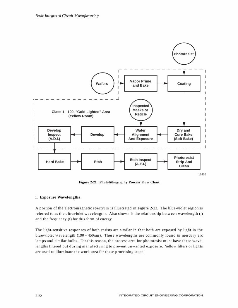
i. Exposure Wavelengths
A portion of the electromagnetic spectrum is illustrated in Figure 2-23. The blue-violet region isreferred to as the ultraviolet wavelengths. Also shown is the relationship between wavelength (l)and the frequency (f) for this form of energy.
The light-sensitive responses of both resists are similar in that both are exposed by light in theblue-violet wavelength (190 - 450nm). These wavelengths are commonly found in mercury arclamps and similar bulbs. For this reason, the process area for photoresist must have these wave-lengths filtered out during manufacturing to prevent unwanted exposure. Yellow filters or lightsare used to illuminate the work area for these processing steps.
Basic Integrated Circuit Manufacturing
INTEGRATED CIRCUIT ENGINEERING CORPORATION2-22
InspectedMasks or
Reticle
Photoresist
Vapor Primeand Bake Coating
DevelopInspect(A.D.I.)
DevelopWafer
AlignmentAnd Exposure
Dry andCure Bake(Soft Bake)
Hard Bake Etch Etch Inspect(A.E.I.)
PhotoresistStrip And
Clean
1146E
Wafers
Class 1 - 100, "Gold Lighted" Area(Yellow Room)
Figure 2-21. Photolithography Process Flow Chart
Basic Integrated Circuit Manufacturing
INTEGRATED CIRCUIT ENGINEERING CORPORATION 2-23
Etching and Stripping
Resist Negative ResistPositive Resist
Developing
Substrate
Thin Film
Resist
IrradiationRegion
MaskExposing Radiation
7417ASource: ICE
Actinic: The property of radiant energy, especially in the visible and ultra-violet spectral regions, by which chemical changes are produced.
Figure 2-22. Characteristic of Negative and Positive Resists
10–2
100µ10–3
10µ10–4
1µ10–5
0.1µ10–6
0.01µ10–7
0.001µ10–8
0.0001µ
1013 1014 1015 1016 1017 1018
Vis
ible
Lig
ht
Reg
ion
Wavelength (in cm)
Frequencies
Infrared Ultraviolet X-Rays
18069B
Figure 2-23. Part of the Electromagnetic Spectrum
ii. Photoresist Parameters
Photoresist is typically characterized by several parameters that affect its performance. These are:
1. adhesion2. etch resistance3. resolution4. photo sensitivity5. step coverage
b. Wafer Preparation Before Photoresist Application
i. Cleaning
The photoresist process is extremely sensitive to any form of contamination on the surface of thewafer prior to applying the photoresist. To assure the best surface possible, various cleaning tech-niques are often used prior to the priming process. The cleaning process may be some type ofwafer scrubbing (brush or high pressure), chemical cleaning with agitation, or chemical cleaningonly.
ii. Priming
The surface of the silicon substrate can have various layers depending on where in the manufac-turing cycle the current operation resides. Each layer on the silicon surface has a different effecton photoresist adhesion. To provide better adhesion, a process step called priming is performed.The use of a priming solution increases the adhesion of the photoresist to the surface. Primersmay be applied by immersing the substrates in the priming solution, spraying the solution on, orby passing a priming vapor over the surface of the wafer. Some primers have to be baked beforesubsequently coating the wafers with photoresist. Other priming techniques require that thewafer surface be dehydrated at elevated temperatures prior to applying the priming solution.
c. Photoresist Application
Photoresist may be applied to the surface of the wafer using a variety of techniques. These tech-niques include dipping, spraying, brushing, roller coating, and spin coating. Spin coating is themethod most often used in the fabrication of semiconductors.
The spin coating process applies a resist layer to the silicon substrate as uniform as possible forthe required thickness. The uniformity of the coating is very important. As the wafers progressfurther through the manufacturing cycle, the topology of the surface continues to change in thick-ness above the silicon surface. The variation in the vertical heights causes some variation in theresist thickness uniformity.
Basic Integrated Circuit Manufacturing
INTEGRATED CIRCUIT ENGINEERING CORPORATION2-24
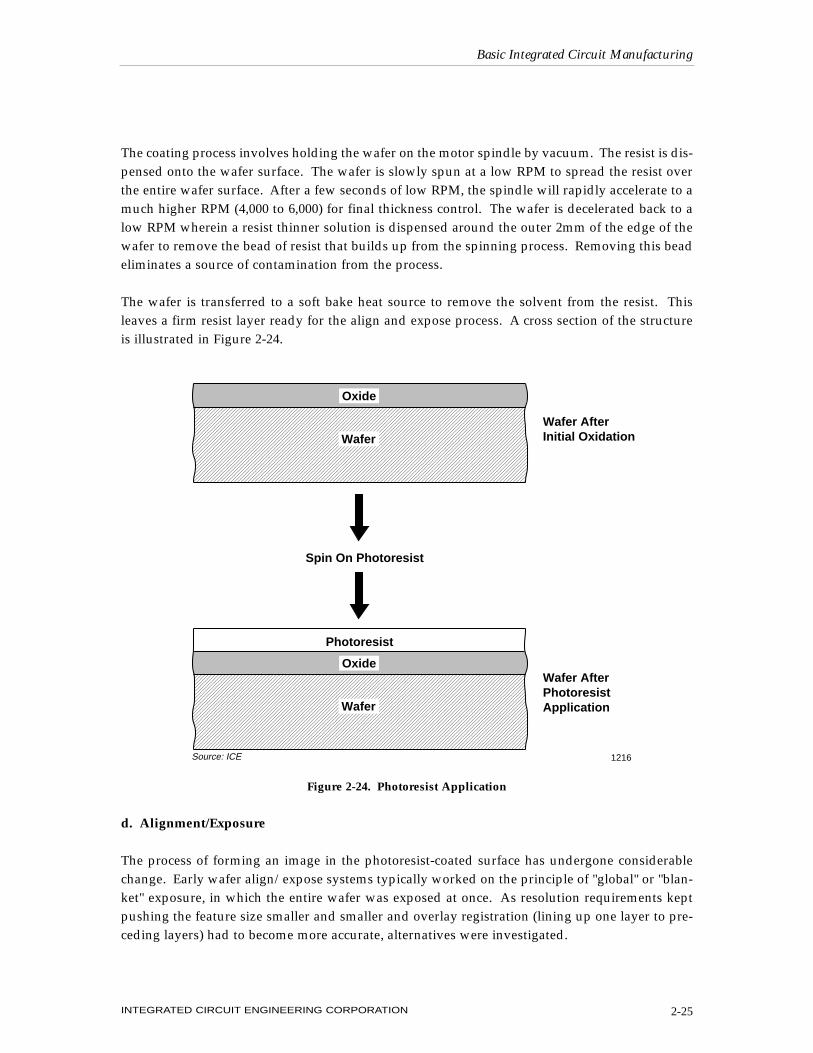
The coating process involves holding the wafer on the motor spindle by vacuum. The resist is dis-pensed onto the wafer surface. The wafer is slowly spun at a low RPM to spread the resist overthe entire wafer surface. After a few seconds of low RPM, the spindle will rapidly accelerate to amuch higher RPM (4,000 to 6,000) for final thickness control. The wafer is decelerated back to alow RPM wherein a resist thinner solution is dispensed around the outer 2mm of the edge of thewafer to remove the bead of resist that builds up from the spinning process. Removing this beadeliminates a source of contamination from the process.
The wafer is transferred to a soft bake heat source to remove the solvent from the resist. Thisleaves a firm resist layer ready for the align and expose process. A cross section of the structureis illustrated in Figure 2-24.
d. Alignment/Exposure
The process of forming an image in the photoresist-coated surface has undergone considerablechange. Early wafer align/expose systems typically worked on the principle of "global" or "blan-ket" exposure, in which the entire wafer was exposed at once. As resolution requirements keptpushing the feature size smaller and smaller and overlay registration (lining up one layer to pre-ceding layers) had to become more accurate, alternatives were investigated.
Basic Integrated Circuit Manufacturing
INTEGRATED CIRCUIT ENGINEERING CORPORATION 2-25
Spin On Photoresist
Photoresist
Oxide
Wafer
Oxide
Wafer
1216Source: ICE
Wafer AfterInitial Oxidation
Wafer AfterPhotoresistApplication
Figure 2-24. Photoresist Application
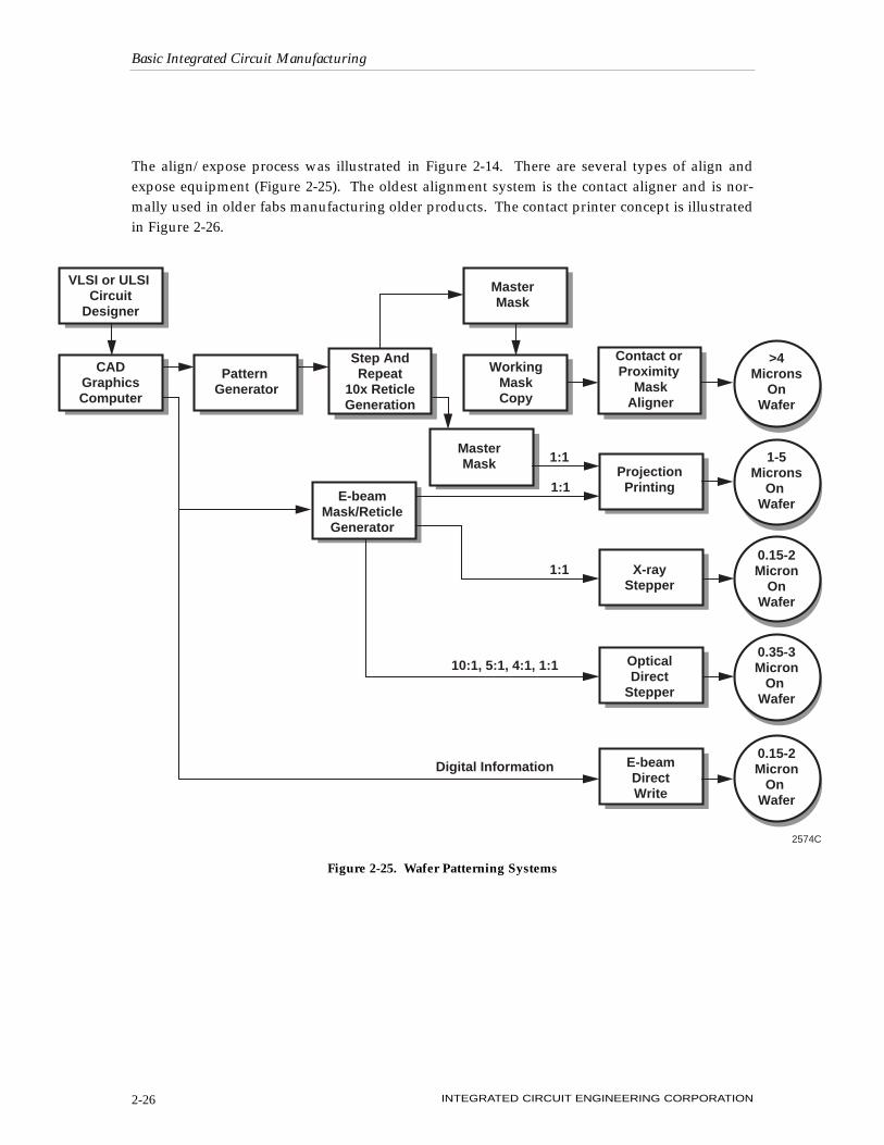
The align/expose process was illustrated in Figure 2-14. There are several types of align andexpose equipment (Figure 2-25). The oldest alignment system is the contact aligner and is nor-mally used in older fabs manufacturing older products. The contact printer concept is illustratedin Figure 2-26.
Basic Integrated Circuit Manufacturing
INTEGRATED CIRCUIT ENGINEERING CORPORATION2-26
VLSI or ULSI Circuit
Designer
CADGraphicsComputer
Pattern Generator
E-beamMask/Reticle
Generator
1:1
1:1
1:1
10:1, 5:1, 4:1, 1:1
Digital Information
2574C
Step AndRepeat
10x ReticleGeneration
WorkingMaskCopy
Contact or Proximity
MaskAligner
X-rayStepper
OpticalDirect
Stepper
E-beamDirectWrite
ProjectionPrinting
1-5Microns
On Wafer
0.15-2Micron
OnWafer
0.35-3Micron
On Wafer
0.15-2Micron
On Wafer
>4Microns
OnWafer
MasterMask
MasterMask
Figure 2-25. Wafer Patterning Systems
i. Contact Aligner
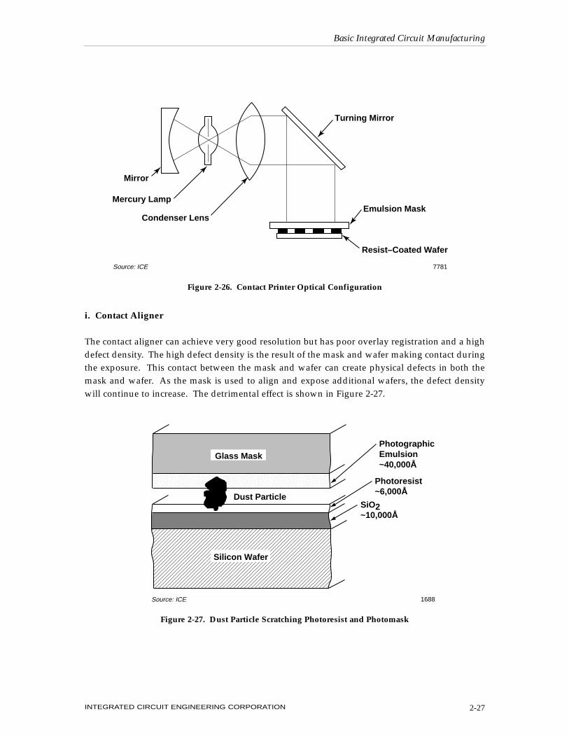
The contact aligner can achieve very good resolution but has poor overlay registration and a highdefect density. The high defect density is the result of the mask and wafer making contact duringthe exposure. This contact between the mask and wafer can create physical defects in both themask and wafer. As the mask is used to align and expose additional wafers, the defect densitywill continue to increase. The detrimental effect is shown in Figure 2-27.
Basic Integrated Circuit Manufacturing
INTEGRATED CIRCUIT ENGINEERING CORPORATION 2-27
Mirror
Mercury Lamp
Condenser LensEmulsion Mask
Resist–Coated Wafer
Turning Mirror
7781Source: ICE
Figure 2-26. Contact Printer Optical Configuration
Dust Particle
SiO2~10,000Å
PhotographicEmulsion~40,000Å
Photoresist~6,000Å
Silicon Wafer
Glass Mask
1688Source: ICE
Figure 2-27. Dust Particle Scratching Photoresist and Photomask
ii. Proximity Printing
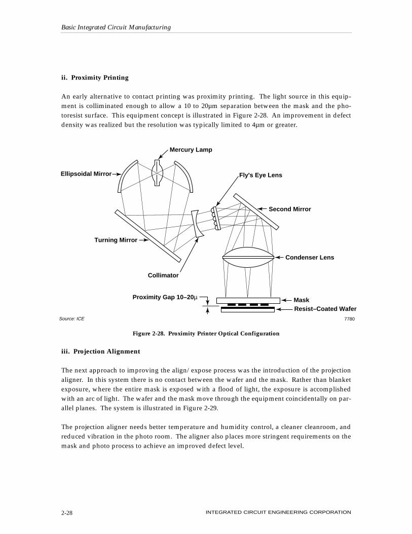
An early alternative to contact printing was proximity printing. The light source in this equip-ment is colliminated enough to allow a 10 to 20µm separation between the mask and the pho-toresist surface. This equipment concept is illustrated in Figure 2-28. An improvement in defectdensity was realized but the resolution was typically limited to 4µm or greater.
iii. Projection Alignment
The next approach to improving the align/expose process was the introduction of the projectionaligner. In this system there is no contact between the wafer and the mask. Rather than blanketexposure, where the entire mask is exposed with a flood of light, the exposure is accomplishedwith an arc of light. The wafer and the mask move through the equipment coincidentally on par-allel planes. The system is illustrated in Figure 2-29.
The projection aligner needs better temperature and humidity control, a cleaner cleanroom, andreduced vibration in the photo room. The aligner also places more stringent requirements on themask and photo process to achieve an improved defect level.
Basic Integrated Circuit Manufacturing
INTEGRATED CIRCUIT ENGINEERING CORPORATION2-28
Mercury Lamp
Fly's Eye Lens
Second Mirror
Condenser Lens
MaskResist–Coated Wafer
Collimator
Proximity Gap 10–20µ
Turning Mirror
Ellipsoidal Mirror
7780Source: ICE
Figure 2-28. Proximity Printer Optical Configuration
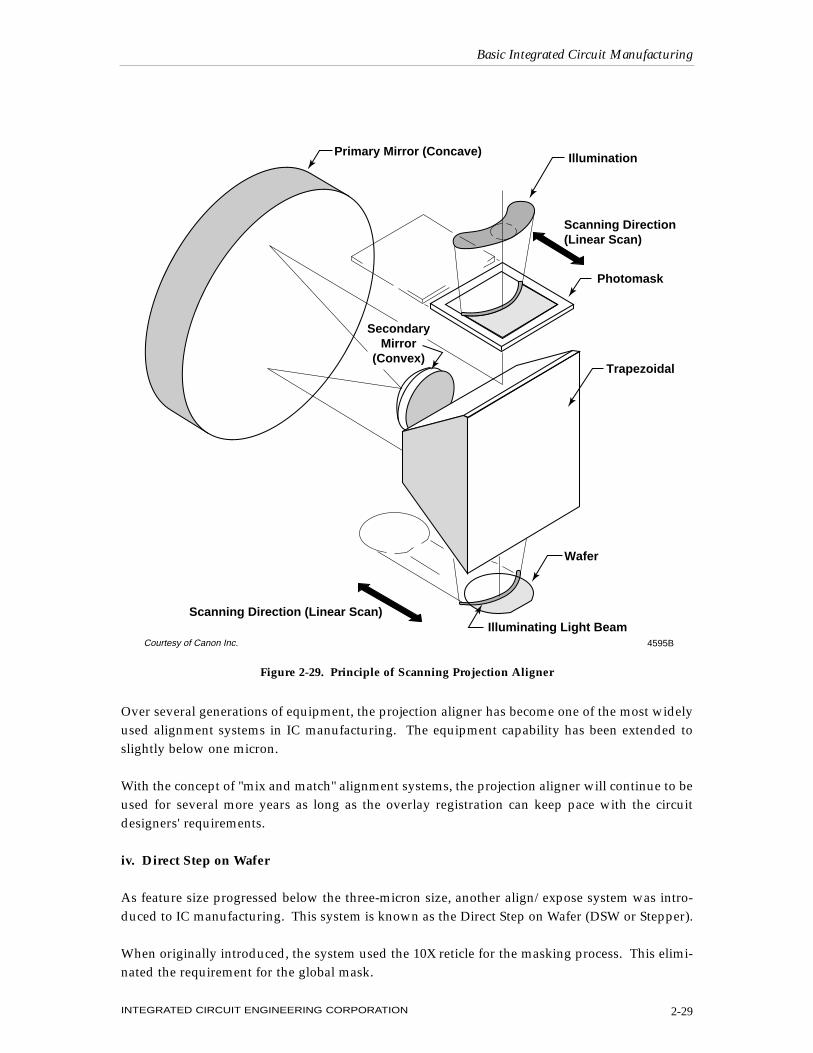
Over several generations of equipment, the projection aligner has become one of the most widelyused alignment systems in IC manufacturing. The equipment capability has been extended toslightly below one micron.
With the concept of "mix and match" alignment systems, the projection aligner will continue to beused for several more years as long as the overlay registration can keep pace with the circuitdesigners' requirements.
iv. Direct Step on Wafer
As feature size progressed below the three-micron size, another align/expose system was intro-duced to IC manufacturing. This system is known as the Direct Step on Wafer (DSW or Stepper).
When originally introduced, the system used the 10X reticle for the masking process. This elimi-nated the requirement for the global mask.
Basic Integrated Circuit Manufacturing
INTEGRATED CIRCUIT ENGINEERING CORPORATION 2-29
Wafer
Illuminating Light BeamScanning Direction (Linear Scan)
SecondaryMirror
(Convex)
Primary Mirror (Concave)
Trapezoidal
Photomask
Scanning Direction(Linear Scan)
Illumination
4595BCourtesy of Canon Inc.
Figure 2-29. Principle of Scanning Projection Aligner
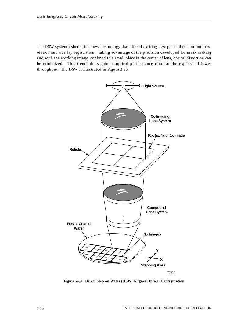
The DSW system ushered in a new technology that offered exciting new possibilities for both res-olution and overlay registration. Taking advantage of the precision developed for mask makingand with the working image confined to a small place in the center of lens, optical distortion canbe minimized. This tremendous gain in optical performance came at the expense of lowerthroughput. The DSW is illustrated in Figure 2-30.
Basic Integrated Circuit Manufacturing
INTEGRATED CIRCUIT ENGINEERING CORPORATION2-30
X
Y
1x Images
Compound Lens System
Resist-CoatedWafer
Stepping Axes
10x, 5x, 4x or 1x Image
Reticle
CollimatingLens System
Light Source
7782A
Figure 2-30. Direct Step on Wafer (DSW) Aligner Optical Configuration
• Mix and Match
DSW has rapidly gained acceptance but the disadvantage of lower production rates has requiredlarger capital investments. To balance between these two conflicting requirements, the concept of"mix and match" evolved as a reasonable compromise.
In mix-and-match lithography, the scanning projection aligner is used for the less critical levels,and the DSW systems are designated for the more critical mask layers. The net result is betteroverall yield and a more cost effective capital investment.
To further address the throughput issue, stepper technology found alternative solutions tothroughput by reducing the lens magnification. This led to the 5X, 4X and 1X DSW technology.Each of these magnifications has its own compromise but at a slightly improved throughput rateas they decline from 10 to 1.
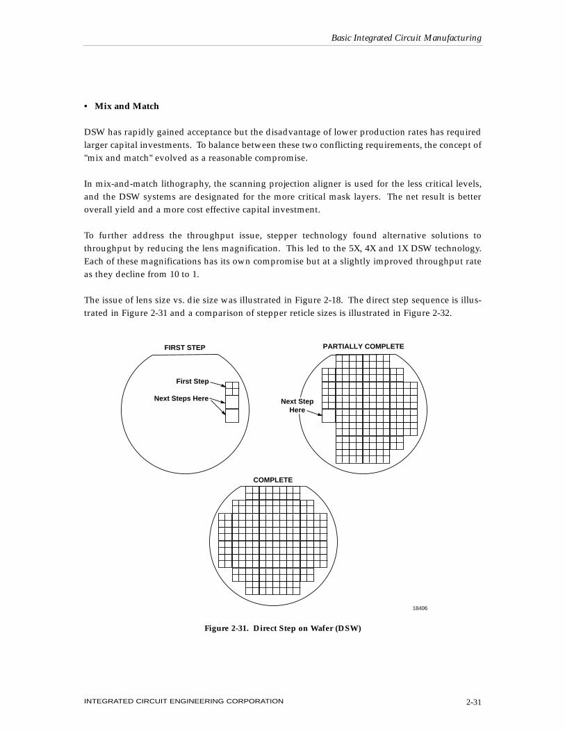
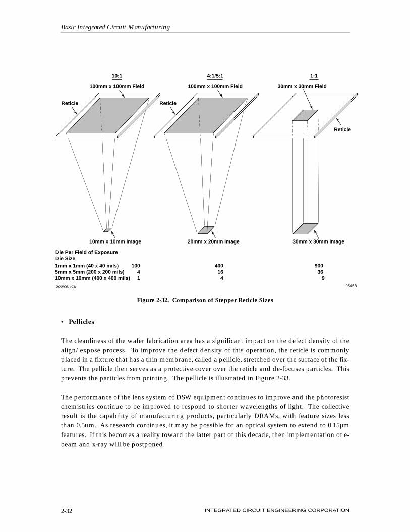
The issue of lens size vs. die size was illustrated in Figure 2-18. The direct step sequence is illus-trated in Figure 2-31 and a comparison of stepper reticle sizes is illustrated in Figure 2-32.
Basic Integrated Circuit Manufacturing
INTEGRATED CIRCUIT ENGINEERING CORPORATION 2-31
FIRST STEP PARTIALLY COMPLETE
COMPLETE
First Step
Next Steps Here
18406
Next StepHere
Figure 2-31. Direct Step on Wafer (DSW)
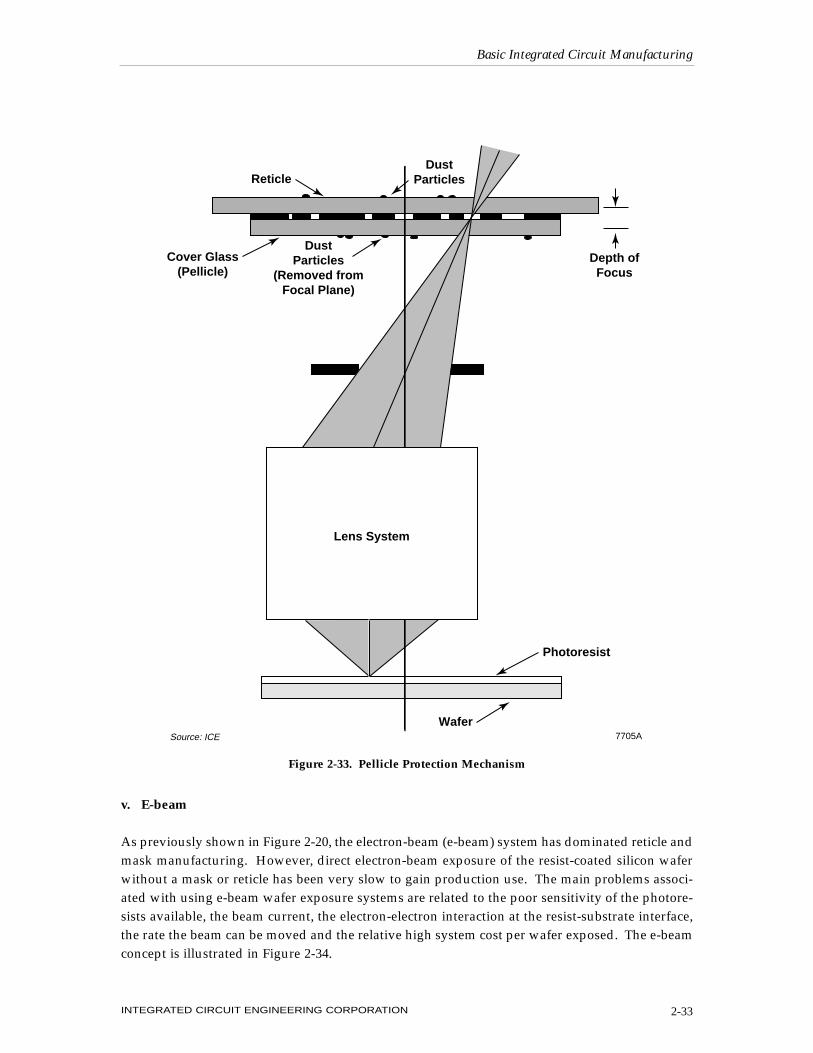
• Pellicles
The cleanliness of the wafer fabrication area has a significant impact on the defect density of thealign/expose process. To improve the defect density of this operation, the reticle is commonlyplaced in a fixture that has a thin membrane, called a pellicle, stretched over the surface of the fix-ture. The pellicle then serves as a protective cover over the reticle and de-focuses particles. Thisprevents the particles from printing. The pellicle is illustrated in Figure 2-33.
The performance of the lens system of DSW equipment continues to improve and the photoresistchemistries continue to be improved to respond to shorter wavelengths of light. The collectiveresult is the capability of manufacturing products, particularly DRAMs, with feature sizes lessthan 0.5um. As research continues, it may be possible for an optical system to extend to 0.15µmfeatures. If this becomes a reality toward the latter part of this decade, then implementation of e-beam and x-ray will be postponed.
Basic Integrated Circuit Manufacturing
INTEGRATED CIRCUIT ENGINEERING CORPORATION2-32
100mm x 100mm Field
10:1
Reticle
10mm x 10mm Image
Die Per Field of ExposureDie Size
100mm x 100mm Field
4:1/5:1
Reticle
20mm x 20mm Image
30mm x 30mm Field
1:1
Reticle
30mm x 30mm Image
1mm x 1mm (40 x 40 mils) 100 400 9005mm x 5mm (200 x 200 mils) 4 16 3610mm x 10mm (400 x 400 mils) 1 4 9
9545BSource: ICE
Figure 2-32. Comparison of Stepper Reticle Sizes
v. E-beam
As previously shown in Figure 2-20, the electron-beam (e-beam) system has dominated reticle andmask manufacturing. However, direct electron-beam exposure of the resist-coated silicon waferwithout a mask or reticle has been very slow to gain production use. The main problems associ-ated with using e-beam wafer exposure systems are related to the poor sensitivity of the photore-sists available, the beam current, the electron-electron interaction at the resist-substrate interface,the rate the beam can be moved and the relative high system cost per wafer exposed. The e-beamconcept is illustrated in Figure 2-34.
Basic Integrated Circuit Manufacturing
INTEGRATED CIRCUIT ENGINEERING CORPORATION 2-33
Reticle
Cover Glass(Pellicle)
DustParticles
(Removed fromFocal Plane)
DustParticles
Depth ofFocus
Photoresist
Wafer7705ASource: ICE
Lens System
Figure 2-33. Pellicle Protection Mechanism
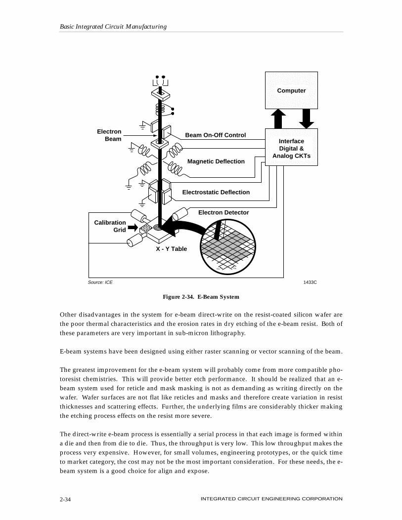
Other disadvantages in the system for e-beam direct-write on the resist-coated silicon wafer arethe poor thermal characteristics and the erosion rates in dry etching of the e-beam resist. Both ofthese parameters are very important in sub-micron lithography.
E-beam systems have been designed using either raster scanning or vector scanning of the beam.
The greatest improvement for the e-beam system will probably come from more compatible pho-toresist chemistries. This will provide better etch performance. It should be realized that an e-beam system used for reticle and mask masking is not as demanding as writing directly on thewafer. Wafer surfaces are not flat like reticles and masks and therefore create variation in resistthicknesses and scattering effects. Further, the underlying films are considerably thicker makingthe etching process effects on the resist more severe.
The direct-write e-beam process is essentially a serial process in that each image is formed withina die and then from die to die. Thus, the throughput is very low. This low throughput makes theprocess very expensive. However, for small volumes, engineering prototypes, or the quick timeto market category, the cost may not be the most important consideration. For these needs, the e-beam system is a good choice for align and expose.
Basic Integrated Circuit Manufacturing
INTEGRATED CIRCUIT ENGINEERING CORPORATION2-34
0.1µ 0.1µ
Computer
InterfaceDigital &
Analog CKTs
Beam On-Off Control
Magnetic Deflection
Electrostatic Deflection
Electron Detector
X - Y Table
CalibrationGrid
ElectronBeam
1433CSource: ICE
Figure 2-34. E-Beam System
vi. X-ray
X-ray energy is another possibility as an align/expose system for imaging on wafers coated withphotoresist sensitive to x-rays. X-rays have very short wavelengths thereby making possibleimproved resolution. Because of the very short wavelength relationship to improved resolution,x-ray technology continues to be actively pursued as an imaging technology for the future.
• X-ray Sources
The energy for an x-ray system comes from either high-energy sources like the synchrotron ringor electron impact low-energy sources. The synchrotron ring puts out a wide spectrum of radia-tion from the infrared region down to the very short wavelengths of x-rays. Beamlines are usedto access this form of radiation.
The impact source of x-rays also delivers a broad spectrum of wavelengths by directing an elec-tron beam at a target material. The x-ray radiation given off by the electron-beam impact matchesthe physical constants of the material and is generally below the intensity of the synchrotronsource.
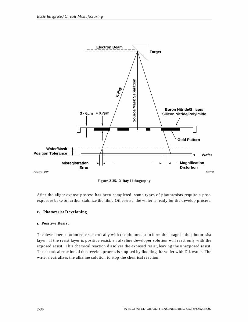
X-ray exposure has been used for full field proximity, 1:1 projection, and step and repeat. As inoptical technology, x-ray stepping can take advantage of greater uniformity radiation in a smallerfield size and greater intensity of energy. Full field x-ray is optimized for throughput at the expenseof overlay registration and pattern resolution. The impact concept is illustrated in Figure 2-35.
• X-ray Masks and Reticles
A serious limitation to the x-ray method of image transfer is in the mask or reticle creation. Thepenetration power of the x-ray energy imposes severe restrictions on the materials used for reti-cles or masks (Figure 2-35). This causes the tooling cost for the mask or reticle to be three to fivetimes the cost of optical masks or reticles. At this stage of development the slight difference in thespectral output between the synchrotron (0.05 to 0.5nm) and the electron impact (0.8 to 2.2nm) haseffect on this tooling cost.
vii. Summary
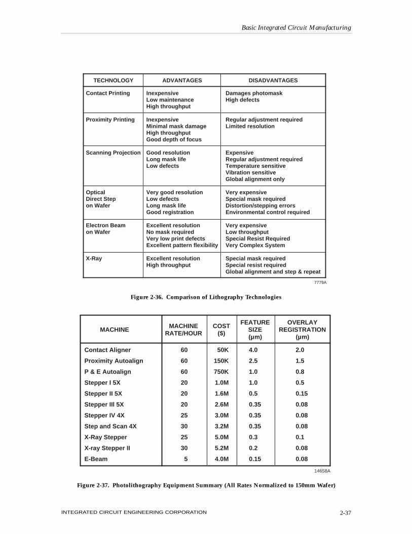
A comparison of lithography technologies is shown in Figure 2-36. A comparison of throughput,capital cost, feature size and overlay registration is summarized in Figure 2-37.
The image transfer process is constantly undergoing change and refinements. Some of these activi-ties are found in multilayer resist patterning, contrast enhancement techniques, the use of anti-reflec-tive coatings, chemical amplification of the resists and adding chemical dyes to the resists. Thesetechniques and others to follow in the future will allow further improvements to be made. The netresult will be smaller feature sizes, higher levels of integration, and more complex integrated circuits.
Basic Integrated Circuit Manufacturing
INTEGRATED CIRCUIT ENGINEERING CORPORATION 2-35
After the align/expose process has been completed, some types of photoresists require a post-exposure bake to further stabilize the film. Otherwise, the wafer is ready for the develop process.
e. Photoresist Developing
i. Positive Resist
The developer solution reacts chemically with the photoresist to form the image in the photoresistlayer. If the resist layer is positive resist, an alkaline developer solution will react only with theexposed resist. This chemical reaction dissolves the exposed resist, leaving the unexposed resist.The chemical reaction of the develop process is stopped by flooding the wafer with D.I. water. Thewater neutralizes the alkaline solution to stop the chemical reaction.
Basic Integrated Circuit Manufacturing
INTEGRATED CIRCUIT ENGINEERING CORPORATION2-36
Gold Pattern
MagnificationDistortion
Wafer
3 - 6µm ≈ 0.7µmX
-Ray
So
urc
e/M
ask
Sep
arat
ion
TargetElectron Beam
Boron Nitride/Silicon/Silicon Nitride/Polyimide
Wafer/MaskPosition Tolerance
MisregistrationError
Source: ICE 3275B
Figure 2-35. X-Ray Lithography
Basic Integrated Circuit Manufacturing
INTEGRATED CIRCUIT ENGINEERING CORPORATION 2-37
TECHNOLOGY ADVANTAGES DISADVANTAGES
Contact Printing
Proximity Printing
Scanning Projection
Optical Direct Step on Wafer
Electron Beam on Wafer
X-Ray
InexpensiveLow maintenanceHigh throughput
Inexpensive Minimal mask damageHigh throughputGood depth of focus
Good resolutionLong mask lifeLow defects
Very good resolutionLow defectsLong mask lifeGood registration
Excellent resolutionNo mask requiredVery low print defectsExcellent pattern flexibility
Excellent resolutionHigh throughput
Damages photomaskHigh defects
Regular adjustment requiredLimited resolution
ExpensiveRegular adjustment requiredTemperature sensitiveVibration sensitiveGlobal alignment only
Very expensiveSpecial mask requiredDistortion/stepping errorsEnvironmental control required
Very expensiveLow throughputSpecial Resist RequiredVery Complex System
Special mask requiredSpecial resist requiredGlobal alignment and step & repeat
7779A
Figure 2-36. Comparison of Lithography Technologies
MACHINERATE/HOURMACHINE COST
($)
FEATURESIZE(µm)
OVERLAYREGISTRATION
(µm)
Contact Aligner
Proximity Autoalign
P & E Autoalign
Stepper I 5X
Stepper II 5X
Stepper IIl 5X
Stepper IV 4X
Step and Scan 4X
X-Ray Stepper
X-ray Stepper II
E-Beam
60
60
60
20
20
20
25
30
25
30
5
50K
150K
750K
1.0M
1.6M
2.6M
3.0M
3.2M
5.0M
5.2M
4.0M
4.0
2.5
1.0
1.0
0.5
0.35
0.35
0.35
0.3
0.2
0.15
2.0
1.5
0.8
0.5
0.15
0.08
0.08
0.08
0.1
0.08
0.08
14658A
Figure 2-37. Photolithography Equipment Summary (All Rates Normalized to 150mm Wafer)
ii. Negative Resist
Negative resist requires a solvent solution for developing the image. Xylene is the commondeveloper for negative resist. The exposure process causes the negative resist to polymerize. Thepolymerization of the resist renders the resist insoluble in the developer. Thus, only the unex-posed resist is dissolved and washed away. The chemical reaction of the Xylene requires anothersolvent to stop the action. N-butyl acetate is commonly used to neutralize and stop the develop-ing action and stabilize the system.
iii. Developing Methods
There are several methods used to develop the photoresist. The particular method chosen isdetermined by the requirements of feature size and the parameters of the resist system. The morecommonly used methods are immersion (batch develop), spray, and a modified spray systemknown as puddle develop.
• Batch Develop
Batch develop is the oldest method. The wafers are placed in carrier that is not affected by thedeveloper chemical. The carrier is immersed in the developer solution for a given period of time.The wafers are then removed from the developer solution and placed into a second solution tostop the develop process and rinse the wafers.
The batch develop process has gone through many changes and refinements over the years buthas been gradually replaced by one of the spray methods: spray for negative resist and puddlefor positive resist.
• Spray (Puddle) Develop
The spray technique has the advantage of processing one wafer at a time with fresh developersolution, improving the uniformity of the process and allowing the handling of the wafers fromcassette to cassette. This provides excellent productivity.
The conventional spray system used for negative photoresist must be modified for positive resist.The spray system is an adiabatic process. The change in spray pressure between the nozzle andatmosphere causes too much of a temperature change for consistent develop results with positiveresist. To overcome this sensitivity to temperature variation, the puddle technique dispenses thedeveloper solution onto the wafer with a very minimal pressure change. (It is like removing anozzle from a hose). The solution is allowed to flow over the entire surface of the wafer quickly.The puddle of fluid is allowed to stand on the surface for the required develop time wherein aflow of D.I. water floods the surface to neutralize the developer solution. This process has alsobeen refined by controlled temperature of the developer solution, heated wafer holder, multiplepuddles, low-pressure spraying after the puddle step, etc. Consequently, consistent results areachieved with this method.
Basic Integrated Circuit Manufacturing
INTEGRATED CIRCUIT ENGINEERING CORPORATION2-38
iv. Plasma Descum
A process used to further improve the surface to be etched after the develop process is calledPlasma Descum. The Descum process is done by placing the wafer in a plasma system whereinoxygen is injected into the low-pressure process chamber with an applied R.F. field. The R.F.energy ionizes the oxygen and causes a chemical reaction between the resist and the ionizedoxygen. This in effect etches the wafer and removes thin films of resist that may not have beencompletely removed in the develop process, providing a cleaner surface for the etch process.
v. Spin-Dry Process
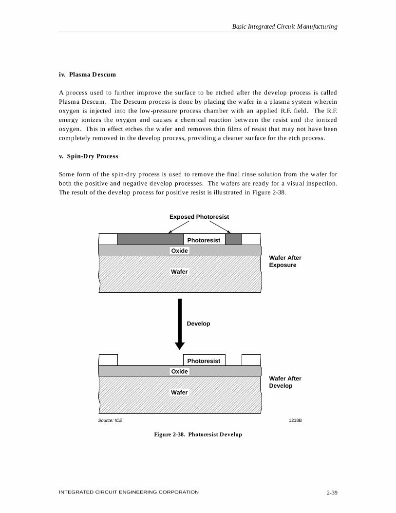
Some form of the spin-dry process is used to remove the final rinse solution from the wafer forboth the positive and negative develop processes. The wafers are ready for a visual inspection.The result of the develop process for positive resist is illustrated in Figure 2-38.
Basic Integrated Circuit Manufacturing
INTEGRATED CIRCUIT ENGINEERING CORPORATION 2-39
Photoresist
Oxide
Wafer
1218BSource: ICE
Wafer AfterDevelop
Photoresist
Oxide
Wafer
Develop
Wafer AfterExposure
Exposed Photoresist
Figure 2-38. Photoresist Develop
vi. Inspection After Develop
Visual inspection of the photoresist-patterned surface is a difficult task. And, as the circuitrybecomes denser, the inspection after develop (ADI) will become even more difficult. Therefore,the photoresist process will rely more on Statistical Process Control and less on the visual inspec-tion.
The current trend in technology for monitoring the develop process after developing is to use pro-grammed pattern recognition visual inspection equipment. This type of automation eliminatesthe eye fatigue problem and provides more consistent results. The automated visual inspectionstation sample inspects using a statistical plan. This provides immediate feedback for manufac-turing control and aids in keeping the rework rate low.
The decision to rework a wafer (or wafers) after the develop inspection has a significant impacton the cycletime of the overall process. Good manufacturing practices dictate keeping reworkslow at this inspection. The long-term goal is to be able to eliminate this inspection through con-tinued improvement by using Statistical Process Control.
vii. Post-Develop (Hard) Bake
After the inspection is completed, the wafers are given a "hard bake" at a temperature of 130°C to160°C to dehydrate the photoresist prior to etch or ion implant processes. This bake stabilizes theresist characteristics and makes the resist less sensitive to these hostile process environments.
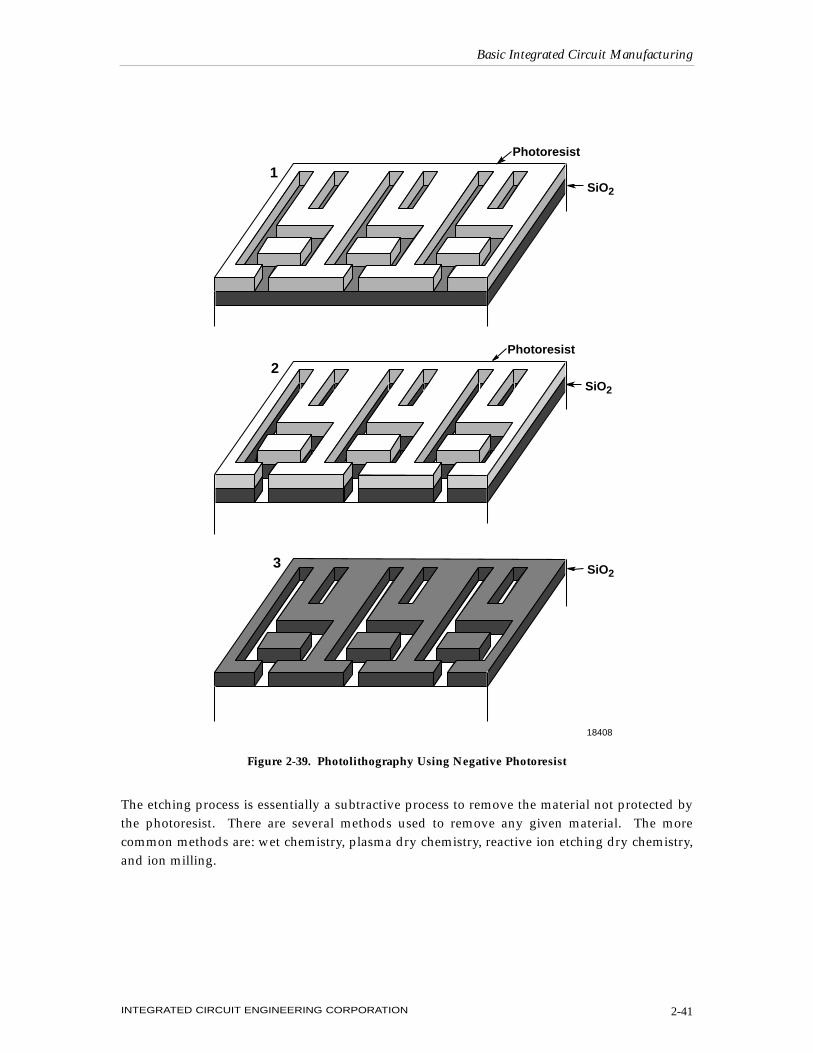
f. Etch
The etching process removes the material not protected by the hardened photoresist. The resultof the etching process was illustrated in Figure 2-15 for positive resist and is shown in Figure 2-39for negative resist.
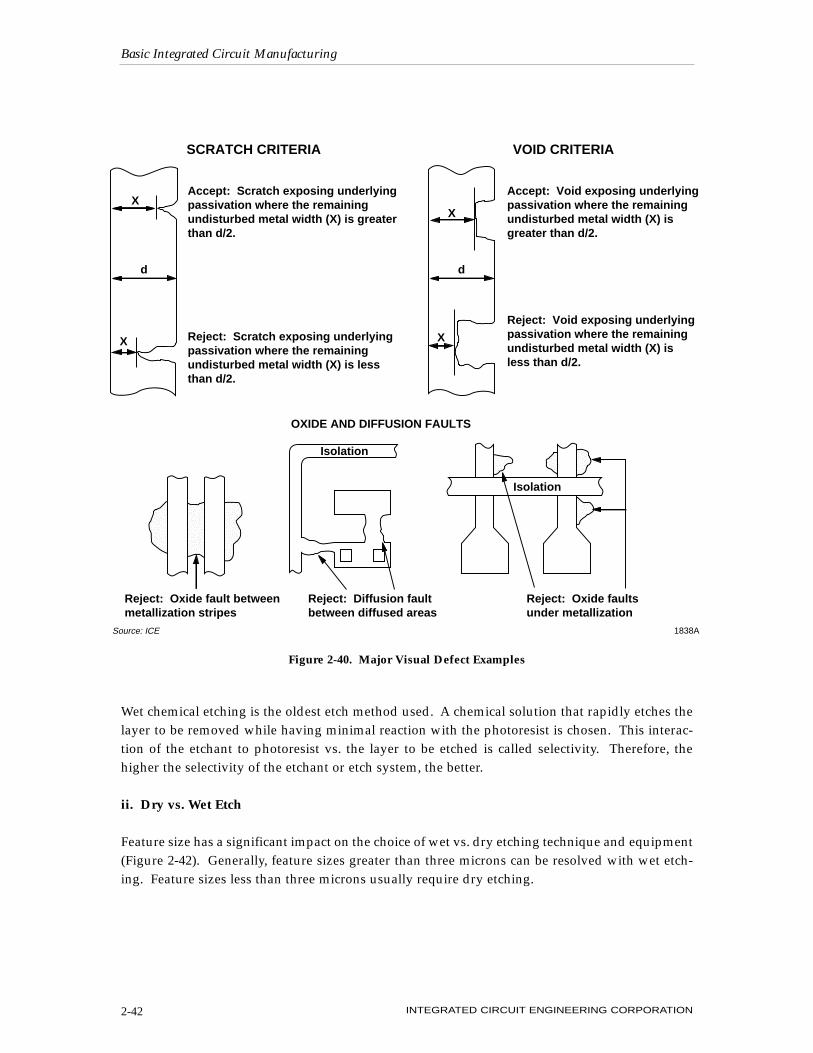
These figures are idealistic representations of the patterning process. In actual manufacturing,there are varying degrees of acceptable results. Figure 2-40 illustrates several examples.
The etching process is divided into two basic methods: isotropic and anisotropic. These termsdescribe the geometrical shape the film will have after the etching process.
i. Isotropic/Anisotropic
An isotropic etch process will etch laterally while etching the material vertically. The worst caseis when the lateral rate is equal to the vertical etch rate. The anisotropic etch will etch only in thevertical direction. These concepts are illustrated in Figure 2-41.
Basic Integrated Circuit Manufacturing
INTEGRATED CIRCUIT ENGINEERING CORPORATION2-40
The etching process is essentially a subtractive process to remove the material not protected bythe photoresist. There are several methods used to remove any given material. The morecommon methods are: wet chemistry, plasma dry chemistry, reactive ion etching dry chemistry,and ion milling.
Basic Integrated Circuit Manufacturing
INTEGRATED CIRCUIT ENGINEERING CORPORATION 2-41
Photoresist
SiO2
18408
Photoresist
SiO2
SiO2
1
2
3
Figure 2-39. Photolithography Using Negative Photoresist
Wet chemical etching is the oldest etch method used. A chemical solution that rapidly etches thelayer to be removed while having minimal reaction with the photoresist is chosen. This interac-tion of the etchant to photoresist vs. the layer to be etched is called selectivity. Therefore, thehigher the selectivity of the etchant or etch system, the better.
ii. Dry vs. Wet Etch
Feature size has a significant impact on the choice of wet vs. dry etching technique and equipment(Figure 2-42). Generally, feature sizes greater than three microns can be resolved with wet etch-ing. Feature sizes less than three microns usually require dry etching.
Basic Integrated Circuit Manufacturing
INTEGRATED CIRCUIT ENGINEERING CORPORATION2-42
X
X
d
X
X
d
SCRATCH CRITERIA
OXIDE AND DIFFUSION FAULTS
VOID CRITERIA
Accept: Scratch exposing underlyingpassivation where the remainingundisturbed metal width (X) is greaterthan d/2.
Accept: Void exposing underlyingpassivation where the remainingundisturbed metal width (X) isgreater than d/2.
Reject: Scratch exposing underlyingpassivation where the remainingundisturbed metal width (X) is lessthan d/2.
Reject: Void exposing underlyingpassivation where the remainingundisturbed metal width (X) isless than d/2.
Reject: Oxide fault betweenmetallization stripes
Reject: Diffusion faultbetween diffused areas
Reject: Oxide faultsunder metallization
Isolation
Isolation
1838ASource: ICE
Figure 2-40. Major Visual Defect Examples
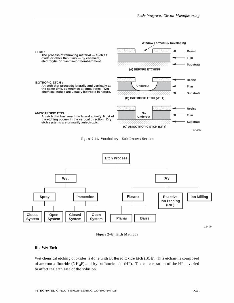
iii. Wet Etch
Wet chemical etching of oxides is done with Buffered Oxide Etch (BOE). This etchant is composedof ammonia fluoride (NH4F) and hydrofluoric acid (HF). The concentration of the HF is variedto affect the etch rate of the solution.
Basic Integrated Circuit Manufacturing
INTEGRATED CIRCUIT ENGINEERING CORPORATION 2-43
Window Formed By Developing
Resist
Film
Substrate
Resist
Film
Substrate
Resist
Film
Substrate
Undercut
NoUndercut
(A) BEFORE ETCHING
(B) ISOTROPIC ETCH (WET)
(C) ANISOTROPIC ETCH (DRY)
14368B
ETCH :The process of removing material — such as oxide or other thin films — by chemical,electrolytic or plasma–ion bombardment.
ISOTROPIC ETCH :An etch that proceeds laterally and vertically at the same time, sometimes at equal rates. W et chemical etches are usually isotropic in nature.
ANISOTROPIC ETCH :An etch that has very little lateral activity . Most of the etching occurs in the vertical direction. Dry etch systems are primarily anisotropic.
Figure 2-41. Vocabulary - Etch Process Section
Etch Process
Wet Dry
Spray Immersion
ClosedSystem
OpenSystem
Plasma
Planar Barrel
ReactiveIon Etching
(RIE)
Ion Milling
18409
ClosedSystem
OpenSystem
Figure 2-42. Etch Methods
Silicon-nitride films are etched with hot phosphoric acid (H3PO4). Generally, the temperature isin the 150°C - 180°C range. Because photoresist does not stand up well at this temperature, thinlayers of silicon dioxide are used on top of the silicon nitride as the etch mask.
Aluminum films are etched with a mixture of phosphoric acid, acetic acid (HAC), and nitric acid(HNO3) diluted with D.I. water. The etch is used in the temperature range of 20°C - 80°C.
Monocrystalline and polycrystalline silicon are etched with a mixture of HF, HNO3, and HAC.The temperature of the solution is maintained in the 20 - 30°C range.
Wet chemical etching can be done by either immersion in a given chemical solution or by spray-ing the chemical onto the surface. After the etching process is completed, the wafers are rinsedwith D.I. water and dried in a spin-dryer.
Unfortunately all of the wet chemical etches leave the edge of the film removed with some degreeof slope.
iv. Dry Etch
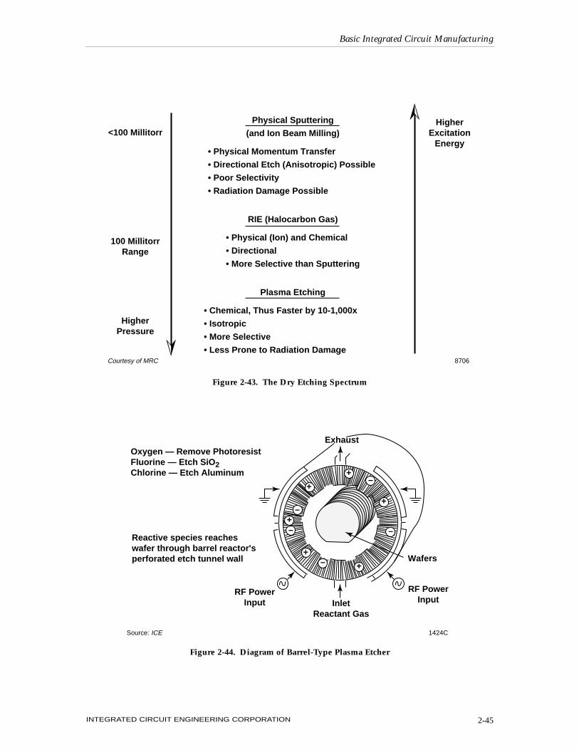
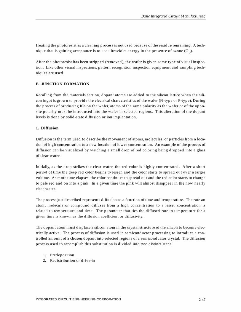
The choice among the use of the various dry etch methods is feature-size driven. The more criti-cal the tolerance, the more likely RIE will be chosen over plasma methods and hardware.
Dry etch processing is performed under some degree of vacuum (Figure 2-43). Dry etch systemsrequire pumping systems for low-pressure operation and gas flow control devices for the variousetchants along with an R.F. power supply and control electronics. These etch systems are morecomplex and require more maintenance than the simpler wet etch stations.
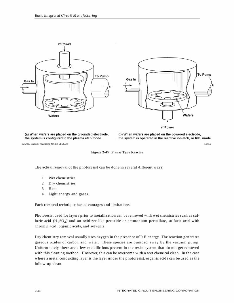
Barrel-type reaction chambers were initially used for plasma etching. This design was acceptablefor removing photoresist but had poor uniformity characteristics for dielectric etching. Theplasma barrel-type etcher is shown in Figure 2-44.
The next generation design was the planar parallel-plate plasma reactor. This improved unifor-mity of etching dielectric layers and led to the lower operating pressure reactive ion etcher (RIE).This is shown in Figure 2-45.
Ion milling systems are still being perfected. The selectivity of the system is poor and the capitalcost is high.
g. Photoresist Removal
At the completion of the etching process, the photoresist is removed. The pattern has now trans-ferred from the mask or reticle into the resist and from the resist into the layer below the resist(Refer back to Figures 2-15 and 2-39). This basic process is repeated for all of the number of layersa particular design requires.
Basic Integrated Circuit Manufacturing
INTEGRATED CIRCUIT ENGINEERING CORPORATION2-44
Basic Integrated Circuit Manufacturing
INTEGRATED CIRCUIT ENGINEERING CORPORATION 2-45
<100 Millitorr
100 MillitorrRange
HigherPressure
Physical Sputtering
(and Ion Beam Milling)
RIE (Halocarbon Gas)
Plasma Etching
• Physical Momentum Transfer
• Directional Etch (Anisotropic) Possible
• Poor Selectivity
• Radiation Damage Possible
• Physical (Ion) and Chemical
• Directional
• More Selective than Sputtering
• Chemical, Thus Faster by 10-1,000x
• Isotropic
• More Selective
• Less Prone to Radiation Damage
HigherExcitation
Energy
8706Courtesy of MRC
Figure 2-43. The Dry Etching Spectrum
+
+
+
+
+
+
–
–
–
–
–
Wafers
RF PowerInputInlet
Reactant Gas
RF PowerInput
1424CSource: ICE
Oxygen — Remove PhotoresistFluorine — Etch SiO2Chlorine — Etch Aluminum
Reactive species reacheswafer through barrel reactor'sperforated etch tunnel wall
Exhaust
Figure 2-44. Diagram of Barrel-Type Plasma Etcher
The actual removal of the photoresist can be done in several different ways.
1. Wet chemistries2. Dry chemistries3. Heat4. Light energy and gases.
Each removal technique has advantages and limitations.
Photoresist used for layers prior to metallization can be removed with wet chemistries such as sul-furic acid (H2SO4) and an oxidizer like peroxide or ammonium persulfate, sulfuric acid withchromic acid, organic acids, and solvents.
Dry chemistry removal usually uses oxygen in the presence of R.F. energy. The reaction generatesgaseous oxides of carbon and water. These species are pumped away by the vacuum pump.Unfortunately, there are a few metallic ions present in the resist system that do not get removedwith this cleaning method. However, this can be overcome with a wet chemical clean. In the casewhere a metal conducting layer is the layer under the photoresist, organic acids can be used as thefollow-up clean.
Basic Integrated Circuit Manufacturing
INTEGRATED CIRCUIT ENGINEERING CORPORATION2-46
To Pump
Wafers
Gas In
rf Power
(a) When wafers are placed on the grounded electrode, the system is configured in the plasma etch mode.
Source: Silicon Processing for the VLSI Era 18410
To Pump
Wafers
Gas In
rf Power
(b) When wafers are placed on the powered electrode, the system is operated in the reactive ion etch, or RIE, mode.
Figure 2-45. Planar Type Reactor
Heating the photoresist as a cleaning process is not used because of the residue remaining. A tech-nique that is gaining acceptance is to use ultraviolet energy in the presence of ozone (O3).
After the photoresist has been stripped (removed), the wafer is given some type of visual inspec-tion. Like other visual inspections, pattern recognition inspection equipment and sampling tech-niques are used.
E. JUNCTION FORMATION
Recalling from the materials section, dopant atoms are added to the silicon lattice when the sili-con ingot is grown to provide the electrical characteristics of the wafer (N-type or P-type). Duringthe process of producing ICs on the wafer, atoms of the same polarity as the wafer or of the oppo-site polarity must be introduced into the wafer in selected regions. This alteration of the dopantlevels is done by solid-state diffusion or ion implantation.
1. Diffusion
Diffusion is the term used to describe the movement of atoms, molecules, or particles from a loca-tion of high concentration to a new location of lower concentration. An example of the process ofdiffusion can be visualized by watching a small drop of red coloring being dropped into a glassof clear water.
Initially, as the drop strikes the clear water, the red color is highly concentrated. After a shortperiod of time the deep red color begins to lessen and the color starts to spread out over a largervolume. As more time elapses, the color continues to spread out and the red color starts to changeto pale red and on into a pink. In a given time the pink will almost disappear in the now nearlyclear water.
The process just described represents diffusion as a function of time and temperature. The rate anatom, molecule or compound diffuses from a high concentration to a lesser concentration isrelated to temperature and time. The parameter that ties the diffused rate to temperature for agiven time is known as the diffusion coefficient or diffusivity.
The dopant atom must displace a silicon atom in the crystal structure of the silicon to become elec-trically active. The process of diffusion is used in semiconductor processing to introduce a con-trolled amount of a chosen dopant into selected regions of a semiconductor crystal. The diffusionprocess used to accomplish this substitution is divided into two distinct steps.
1. Predeposition2. Redistribution or drive-in
Basic Integrated Circuit Manufacturing
INTEGRATED CIRCUIT ENGINEERING CORPORATION 2-47
a. Predeposition
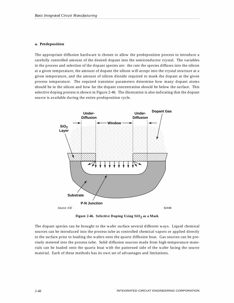
The appropriate diffusion hardware is chosen to allow the predeposition process to introduce acarefully controlled amount of the desired dopant into the semiconductor crystal. The variablesin the process and selection of the dopant species are: the rate the species diffuses into the siliconat a given temperature, the amount of dopant the silicon will accept into the crystal structure at agiven temperature, and the amount of silicon dioxide required to mask the dopant at the givenprocess temperature. The required transistor parameters determine how many dopant atomsshould be in the silicon and how far the dopant concentration should be below the surface. Thisselective doping process is shown in Figure 2-46. The illustration is also indicating that the dopantsource is available during the entire predeposition cycle.
The dopant species can be brought to the wafer surface several different ways. Liquid chemicalsources can be introduced into the process tube as controlled chemical vapors or applied directlyto the surface prior to loading the wafers onto the quartz diffusion boat. Gas sources can be pre-cisely metered into the process tube. Solid diffusion sources made from high-temperature mate-rials can be loaded onto the quartz boat with the patterned side of the wafer facing the sourcematerial. Each of these methods has its own set of advantages and limitations.
Basic Integrated Circuit Manufacturing
INTEGRATED CIRCUIT ENGINEERING CORPORATION2-48
Window
Under-Diffusion
Under-Diffusion
Dopant Gas
P-N Junction
Substrate
SiO2Layer
8244BSource: ICE
Figure 2-46. Selective Doping Using SiO2 as a Mask
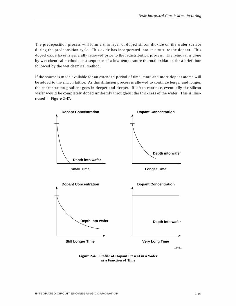
The predeposition process will form a thin layer of doped silicon dioxide on the wafer surfaceduring the predeposition cycle. This oxide has incorporated into its structure the dopant. Thisdoped oxide layer is generally removed prior to the redistribution process. The removal is doneby wet chemical methods or a sequence of a low-temperature thermal oxidation for a brief timefollowed by the wet chemical method.
If the source is made available for an extended period of time, more and more dopant atoms willbe added to the silicon lattice. As this diffusion process is allowed to continue longer and longer,the concentration gradient goes in deeper and deeper. If left to continue, eventually the siliconwafer would be completely doped uniformly throughout the thickness of the wafer. This is illus-trated in Figure 2-47.
Basic Integrated Circuit Manufacturing
INTEGRATED CIRCUIT ENGINEERING CORPORATION 2-49
Dopant Concentration
Depth into wafer
Small Time
Dopant Concentration
Depth into wafer
Longer Time
Dopant Concentration
Depth into wafer
Still Longer Time
Dopant Concentration
Depth into wafer
Very Long Time
18411
Figure 2-47. Profile of Dopant Present in a Waferas a Function of Time
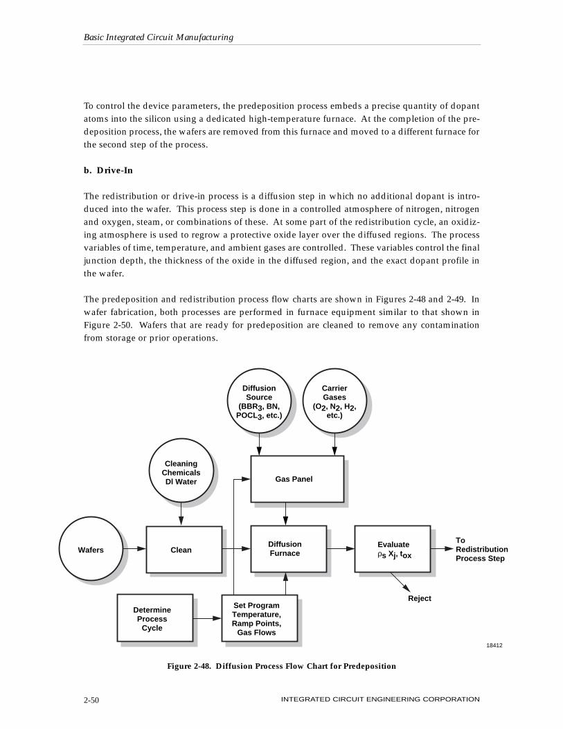
To control the device parameters, the predeposition process embeds a precise quantity of dopantatoms into the silicon using a dedicated high-temperature furnace. At the completion of the pre-deposition process, the wafers are removed from this furnace and moved to a different furnace forthe second step of the process.
b. Drive-In
The redistribution or drive-in process is a diffusion step in which no additional dopant is intro-duced into the wafer. This process step is done in a controlled atmosphere of nitrogen, nitrogenand oxygen, steam, or combinations of these. At some part of the redistribution cycle, an oxidiz-ing atmosphere is used to regrow a protective oxide layer over the diffused regions. The processvariables of time, temperature, and ambient gases are controlled. These variables control the finaljunction depth, the thickness of the oxide in the diffused region, and the exact dopant profile inthe wafer.
The predeposition and redistribution process flow charts are shown in Figures 2-48 and 2-49. Inwafer fabrication, both processes are performed in furnace equipment similar to that shown inFigure 2-50. Wafers that are ready for predeposition are cleaned to remove any contaminationfrom storage or prior operations.
Basic Integrated Circuit Manufacturing
INTEGRATED CIRCUIT ENGINEERING CORPORATION2-50
DiffusionSource
(BBR3, BN,POCL3, etc.)
CarrierGases
(O2, N2, H2,etc.)
Gas Panel
Set ProgramTemperature,Ramp Points,
Gas Flows
DetermineProcess
Cycle
CleanDiffusionFurnace
CleaningChemicalsDl Water
Wafers
Reject
To RedistributionProcess Step
Evaluate ρs Xj, tox
18412
Figure 2-48. Diffusion Process Flow Chart for Predeposition
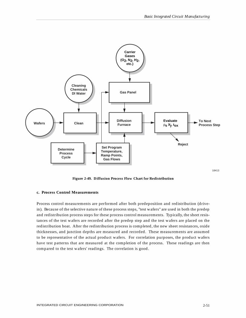
c. Process Control Measurements
Process control measurements are performed after both predeposition and redistribution (drive-in). Because of the selective nature of these process steps, "test wafers" are used in both the predepand redistribution process steps for these process control measurements. Typically, the sheet resis-tances of the test wafers are recorded after the predep step and the test wafers are placed on theredistribution boat. After the redistribution process is completed, the new sheet resistances, oxidethicknesses, and junction depths are measured and recorded. These measurements are assumedto be representative of the actual product wafers. For correlation purposes, the product wafershave test patterns that are measured at the completion of the process. These readings are thencompared to the test wafers' readings. The correlation is good.
Basic Integrated Circuit Manufacturing
INTEGRATED CIRCUIT ENGINEERING CORPORATION 2-51
Gas Panel
Set ProgramTemperature,Ramp Points,
Gas Flows
DetermineProcess
Cycle
CleanDiffusionFurnace
CleaningChemicalsDl Water
Wafers
Reject
To NextProcess Step
18413
CarrierGases
(O2, N2, H2,etc.)
Evaluate ρs Xj, tox
Figure 2-49. Diffusion Process Flow Chart for Redistribution
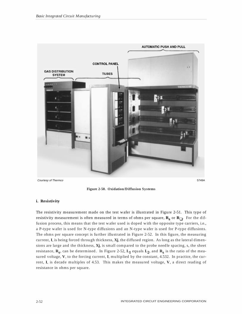
i. Resistivity
The resistivity measurement made on the test wafer is illustrated in Figure 2-51. This type ofresistivity measurement is often measured in terms of ohms per square, Rs or R. For the dif-fusion process, this means that the test wafer used is doped with the opposite type carriers, i.e.,a P-type wafer is used for N-type diffusions and an N-type wafer is used for P-type diffusions.The ohms per square concept is further illustrated in Figure 2-52. In this figure, the measuringcurrent, I, is being forced through thickness, Xj, the diffused region. As long as the lateral dimen-sions are large and the thickness, Xj, is small compared to the probe needle spacing, s, the sheetresistance, Rs, can be determined. In Figure 2-52, L1 equals L2, and Rs is the ratio of the mea-sured voltage, V, to the forcing current, I, multiplied by the constant, 4.532. In practice, the cur-rent, I, is decade multiples of 4.53. This makes the measured voltage, V, a direct reading ofresistance in ohms per square.
Basic Integrated Circuit Manufacturing
INTEGRATED CIRCUIT ENGINEERING CORPORATION2-52
Courtesy of Thermco 5749A
Figure 2-50. Oxidation/Diffusion Systems
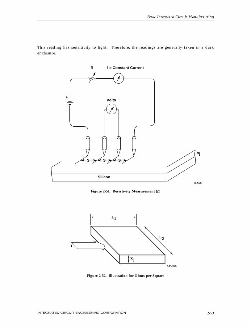
This reading has sensitivity to light. Therefore, the readings are generally taken in a darkenclosure.
Basic Integrated Circuit Manufacturing
INTEGRATED CIRCUIT ENGINEERING CORPORATION 2-53
1L
2L
jX
I
14580A
S S S
Volts
Silicon
l = Constant CurrentR
+
–
1850B
xj
Figure 2-51. Resistivity Measurement (ρ)
Figure 2-52. Illustration for Ohms per Square
ii. Junction Depth
The junction depth measurement, Xj, is made on a test wafer by lapping the wafer at a very shal-low angle. The angle lapping concept is illustrated in Figure 2-53. After lapping, the wafer isetched in a chemical that stains the P region darker than the N region. This difference in color willreflect monochromatic light such that the interference fringes can be counted. Knowing the wave-length of the monochromatic light and the number of fringes allows the junction depth to be deter-mined. Figure 2-54 shows the results of junction staining and monochromatic light on a bipolartransistor. Figure 2-55 illustrates an MOS transistor with the source and drain junctions delin-eated.
2. Ion Implantation
An alternative method for introducing dopant atoms into silicon emerged in the late 1960's. Thisnew development is called ion (an ion is a charged atom) implantation. Essentially, ion implan-tation is the process of shooting ions of the desired dopant species into the wafer through open-ings in the oxide or hardened photoresist.
In contrast to diffusion, ion implantation is a low-temperature technique. It provides a flexibilitynot available with diffusion. The ion implant process takes ions of a desired dopant, acceleratesthem using an electric field, and scans them across the wafer surface to obtain a uniform prede-position. Scanning is the process of the beam moving back and forth across the surface of thewafer. This predep concentration is similar to the predeposition described in the diffusion section,except the dopant does not displace silicon atoms in the silicon lattice after the implant is com-pleted. More on this in a later paragraph.
Basic Integrated Circuit Manufacturing
INTEGRATED CIRCUIT ENGINEERING CORPORATION2-54
Film
Substrate
Where: SIN θ =
θ
Z (SIN θ) = Film Thickness (Y)
θ = 1- 5°
Y
Z
8785BSource: ICE
YZ
Figure 2-53. Angle Lapping Measurement Method
Basic Integrated Circuit Manufacturing
INTEGRATED CIRCUIT ENGINEERING CORPORATION 2-55
Photos by ICE 1851
A. Stained single-junction structure B. Stained doub le-junction structurerevealed b y interf erence fring es. revealed b y interf erence fring es.
Figure 2-54. Monochromatic Light Examinations
10250B
Figure 2-55. Silicon Gate MOS Cross-Section
The first requirement of an ion implantation system is the ability to generate ions of the desiredspecies. A gaseous source containing the dopant atom is fed into a vacuum chamber and ionizedby coming into contact with a hot filament. The correct ions are separated from any other ion gen-erated by bending them a set angle using an electromagnetic field. This separation by atomicmass allows only the desired ions to enter the acceleration tube. The selected ions are accelerated
using an electric field and strike thetarget wafer at some predeterminedhigh-energy level. The ion beampasses through an electro-opticalbeam shaping region of the acceler-ator tube to control the diameter ofthe beam and causes the beam to bescanned. It is a scanned beam thatstrikes the wafer surface and pene-trates inward to some depth. Thebasic concepts are summarized inFigure 2-56. A diagram of an ionimplanter is shown in Figure 2-57.
Basic Integrated Circuit Manufacturing
INTEGRATED CIRCUIT ENGINEERING CORPORATION2-56
Figure 2-56. Basic Concepts of Ion Implant
1. Generation of ions in some kind of source region.
2. Separation of ions by mass to prevent undesired species from reaching the target.
3. Acceleration of the selected ions to high energies.
4. Bombardment of the sample (located in a target chamber) by the high-energy ions.
150kV–+
–+
EquipmentGround
TerminalGround
AccelerationTube
Focus
VacuumSystem
IonSource
90° AnalyzingMagnet
Resolving Aperture
Neutral Beam Trapand Beam Gate
Y-AxisScanner
X-AxisScanner
Wafer inWafer ProcessChamber
Neutral Beam andBeam Path Gated
Beam Trap andGate Plate
1305Source: ICE
Figure 2-57. Configuration of a Typical 200KeV Ion Implanter
1422A
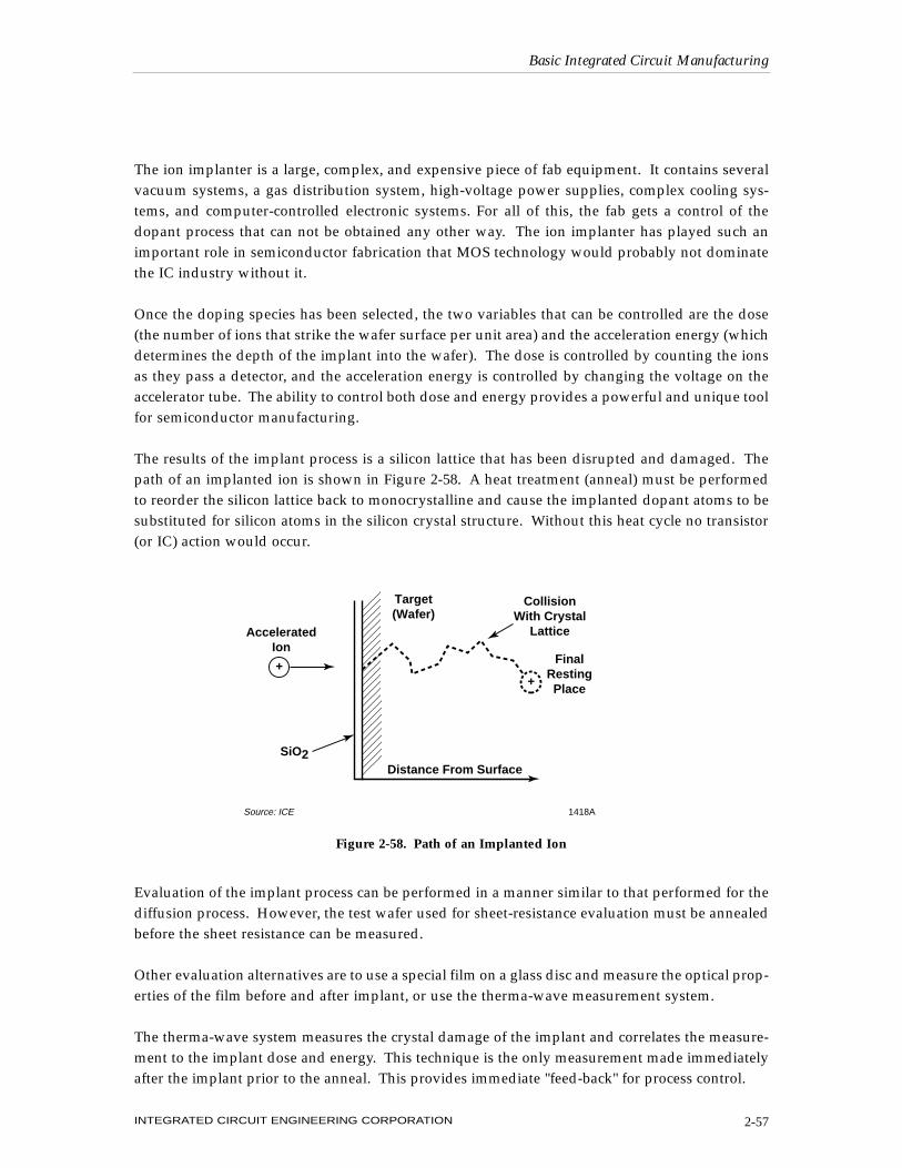
The ion implanter is a large, complex, and expensive piece of fab equipment. It contains severalvacuum systems, a gas distribution system, high-voltage power supplies, complex cooling sys-tems, and computer-controlled electronic systems. For all of this, the fab gets a control of thedopant process that can not be obtained any other way. The ion implanter has played such animportant role in semiconductor fabrication that MOS technology would probably not dominatethe IC industry without it.
Once the doping species has been selected, the two variables that can be controlled are the dose(the number of ions that strike the wafer surface per unit area) and the acceleration energy (whichdetermines the depth of the implant into the wafer). The dose is controlled by counting the ionsas they pass a detector, and the acceleration energy is controlled by changing the voltage on theaccelerator tube. The ability to control both dose and energy provides a powerful and unique toolfor semiconductor manufacturing.
The results of the implant process is a silicon lattice that has been disrupted and damaged. Thepath of an implanted ion is shown in Figure 2-58. A heat treatment (anneal) must be performedto reorder the silicon lattice back to monocrystalline and cause the implanted dopant atoms to besubstituted for silicon atoms in the silicon crystal structure. Without this heat cycle no transistor(or IC) action would occur.
Evaluation of the implant process can be performed in a manner similar to that performed for thediffusion process. However, the test wafer used for sheet-resistance evaluation must be annealedbefore the sheet resistance can be measured.
Other evaluation alternatives are to use a special film on a glass disc and measure the optical prop-erties of the film before and after implant, or use the therma-wave measurement system.
The therma-wave system measures the crystal damage of the implant and correlates the measure-ment to the implant dose and energy. This technique is the only measurement made immediatelyafter the implant prior to the anneal. This provides immediate "feed-back" for process control.
Basic Integrated Circuit Manufacturing
INTEGRATED CIRCUIT ENGINEERING CORPORATION 2-57
AcceleratedIon
Target(Wafer)
CollisionWith Crystal
Lattice
FinalRestingPlace
Distance From Surface
1418ASource: ICE
++
SiO2
Figure 2-58. Path of an Implanted Ion
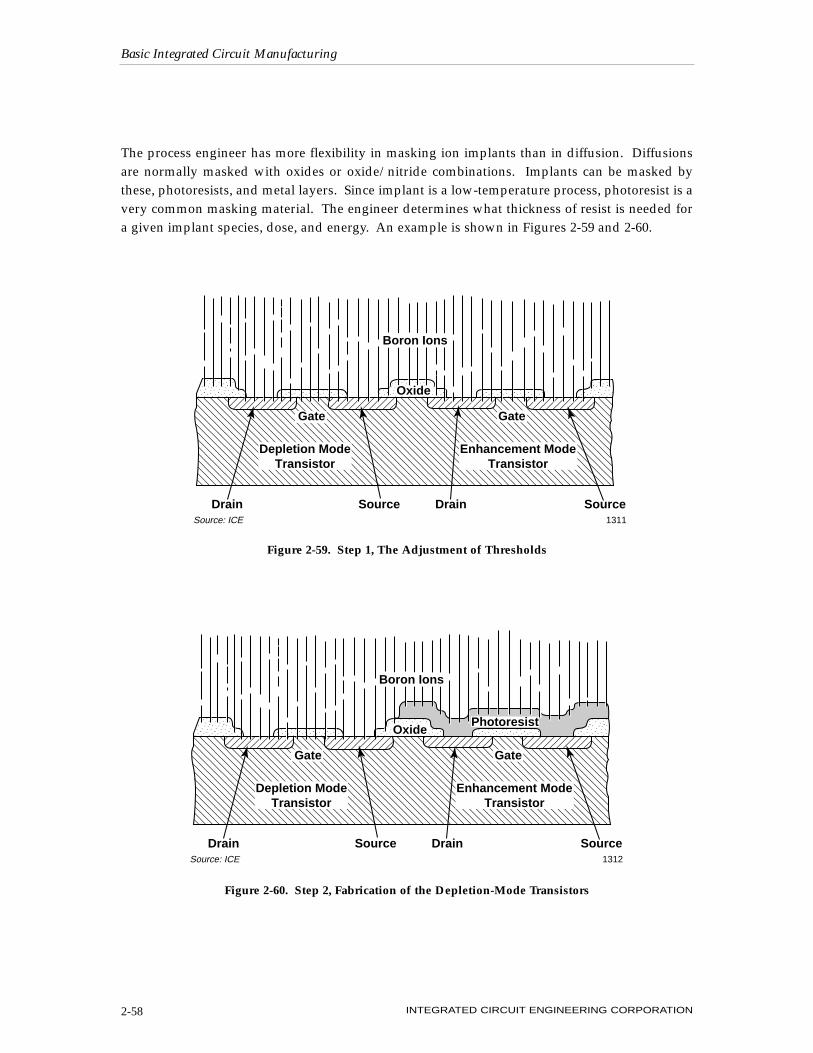
The process engineer has more flexibility in masking ion implants than in diffusion. Diffusionsare normally masked with oxides or oxide/nitride combinations. Implants can be masked bythese, photoresists, and metal layers. Since implant is a low-temperature process, photoresist is avery common masking material. The engineer determines what thickness of resist is needed fora given implant species, dose, and energy. An example is shown in Figures 2-59 and 2-60.
Basic Integrated Circuit Manufacturing
INTEGRATED CIRCUIT ENGINEERING CORPORATION2-58
SourceSource DrainDrain
Depletion ModeTransistor
Enhancement ModeTransistor
Boron Ions
1311Source: ICE
A
Gate Gate
Oxide
Figure 2-59. Step 1, The Adjustment of Thresholds
SourceSource DrainDrain
Depletion ModeTransistor
Enhancement ModeTransistor
Boron Ions
1312Source: ICE
Photoresist
Gate Gate
Oxide
Figure 2-60. Step 2, Fabrication of the Depletion-Mode Transistors
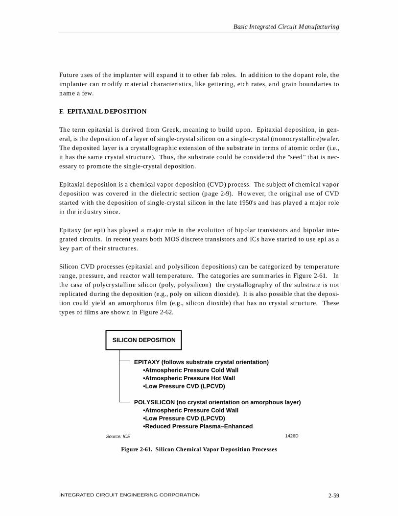
Future uses of the implanter will expand it to other fab roles. In addition to the dopant role, theimplanter can modify material characteristics, like gettering, etch rates, and grain boundaries toname a few.
F. EPITAXIAL DEPOSITION
The term epitaxial is derived from Greek, meaning to build upon. Epitaxial deposition, in gen-eral, is the deposition of a layer of single-crystal silicon on a single-crystal (monocrystalline)wafer.The deposited layer is a crystallographic extension of the substrate in terms of atomic order (i.e.,it has the same crystal structure). Thus, the substrate could be considered the "seed" that is nec-essary to promote the single-crystal deposition.
Epitaxial deposition is a chemical vapor deposition (CVD) process. The subject of chemical vapordeposition was covered in the dielectric section (page 2-9). However, the original use of CVDstarted with the deposition of single-crystal silicon in the late 1950's and has played a major rolein the industry since.
Epitaxy (or epi) has played a major role in the evolution of bipolar transistors and bipolar inte-grated circuits. In recent years both MOS discrete transistors and ICs have started to use epi as akey part of their structures.
Silicon CVD processes (epitaxial and polysilicon depositions) can be categorized by temperaturerange, pressure, and reactor wall temperature. The categories are summaries in Figure 2-61. Inthe case of polycrystalline silicon (poly, polysilicon) the crystallography of the substrate is notreplicated during the deposition (e.g., poly on silicon dioxide). It is also possible that the deposi-tion could yield an amorphorus film (e.g., silicon dioxide) that has no crystal structure. Thesetypes of films are shown in Figure 2-62.
Basic Integrated Circuit Manufacturing
INTEGRATED CIRCUIT ENGINEERING CORPORATION 2-59
SILICON DEPOSITION
EPITAXY (follows substrate crystal orientation)•Atmospheric Pressure Cold Wall•Atmospheric Pressure Hot Wall•Low Pressure CVD (LPCVD)
POLYSILICON (no crystal orientation on amorphous layer)•Atmospheric Pressure Cold Wall•Low Pressure CVD (LPCVD)•Reduced Pressure Plasma–Enhanced
1426DSource: ICE
Figure 2-61. Silicon Chemical Vapor Deposition Processes
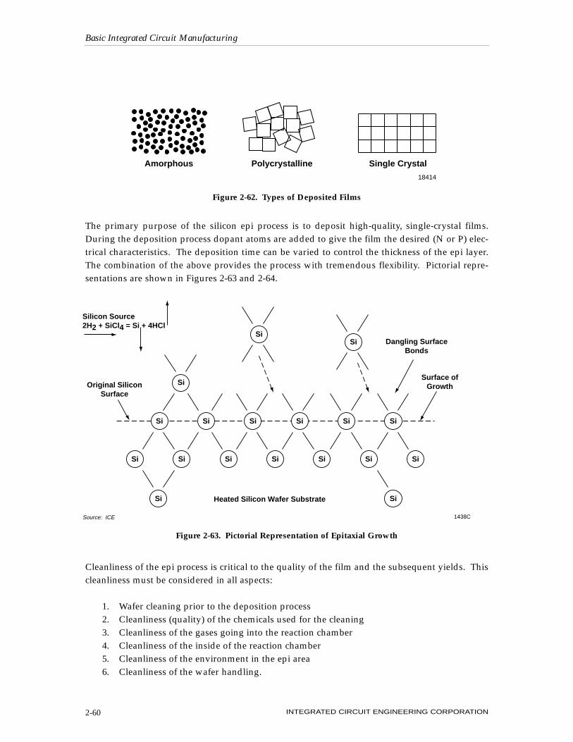
The primary purpose of the silicon epi process is to deposit high-quality, single-crystal films.During the deposition process dopant atoms are added to give the film the desired (N or P) elec-trical characteristics. The deposition time can be varied to control the thickness of the epi layer.The combination of the above provides the process with tremendous flexibility. Pictorial repre-sentations are shown in Figures 2-63 and 2-64.
Cleanliness of the epi process is critical to the quality of the film and the subsequent yields. Thiscleanliness must be considered in all aspects:
1. Wafer cleaning prior to the deposition process2. Cleanliness (quality) of the chemicals used for the cleaning3. Cleanliness of the gases going into the reaction chamber 4. Cleanliness of the inside of the reaction chamber5. Cleanliness of the environment in the epi area6. Cleanliness of the wafer handling.
Basic Integrated Circuit Manufacturing
INTEGRATED CIRCUIT ENGINEERING CORPORATION2-60
Amorphous Polycrystalline Single Crystal
18414
Figure 2-62. Types of Deposited Films
Si
Si
Si Si Si Si Si
Si
Si Si Si Si Si Si Si
SiSi
Si
Heated Silicon Wafer Substrate
Original SiliconSurface
Dangling SurfaceBonds
Surface ofGrowth
Silicon Source2H2 + SiCl4 = Si + 4HCl
1438CSource: ICE
Figure 2-63. Pictorial Representation of Epitaxial Growth
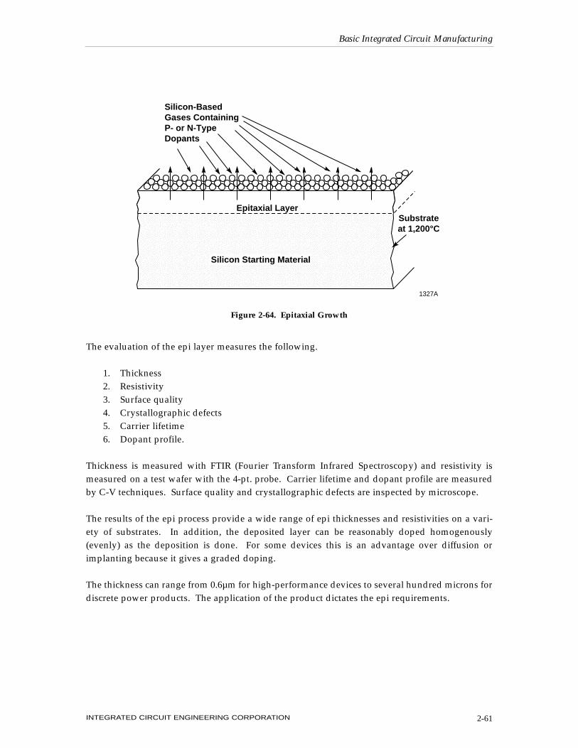
The evaluation of the epi layer measures the following.
1. Thickness2. Resistivity3. Surface quality4. Crystallographic defects5. Carrier lifetime6. Dopant profile.
Thickness is measured with FTIR (Fourier Transform Infrared Spectroscopy) and resistivity ismeasured on a test wafer with the 4-pt. probe. Carrier lifetime and dopant profile are measuredby C-V techniques. Surface quality and crystallographic defects are inspected by microscope.
The results of the epi process provide a wide range of epi thicknesses and resistivities on a vari-ety of substrates. In addition, the deposited layer can be reasonably doped homogenously(evenly) as the deposition is done. For some devices this is an advantage over diffusion orimplanting because it gives a graded doping.
The thickness can range from 0.6µm for high-performance devices to several hundred microns fordiscrete power products. The application of the product dictates the epi requirements.
Basic Integrated Circuit Manufacturing
INTEGRATED CIRCUIT ENGINEERING CORPORATION 2-61
Epitaxial LayerSubstrateat 1,200°C
Silicon-BasedGases ContainingP- or N-TypeDopants
Silicon Starting Material
1327A
Figure 2-64. Epitaxial Growth
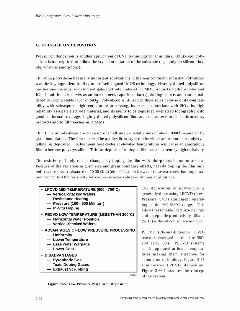
G. POLYSILICON DEPOSITION
Polysilicon deposition is another application of CVD technology for thin films. Unlike epi, poly-silicon is not required to follow the crystal orientation of the substrate (e.g., poly on silicon diox-ide, which is amorphous).
Thin-film polysilicon has many important applications in the semiconductor industry. Polysiliconwas the key ingredient leading to the "self aligned" MOS technology. Heavily-doped polysiliconhas become the most widely used gate-electrode material for MOS products, both discretes andICs. In addition, it serves as an interconnect, capacitor plate(s), doping source, and can be oxi-dized to form a stable layer of SiO2. Polysilicon is utilized in these roles because of its compati-bility with subsequent high-temperature processing, its excellent interface with SiO2, its highreliability as a gate electrode material, and its ability to be deposited over steep topography withgood conformal coverage. Lightly-doped polysilicon films are used as resistors in static memoryproducts and to fill trenches in DRAMs.
Thin films of polysilicon are made up of small single-crystal grains of about 1000Å separated bygrain boundaries. The film that will be a polysilicon layer can be either amorphorus or polycrys-talline "as deposited." Subsequent heat cycles at elevated temperatures will cause an amorphousfilm to become polycrystalline. This "as-deposited" undoped film has an extremely high resistivity.
The resistivity of poly can be changed by doping the film with phorphous, boron, or arsenic.Because of the variation in grain size and grain boundary effects, heavily doping the film onlyreduces the sheet resistance to 10-30 Ω/ (ohms/sq.). In between these extremes, ion implanta-tion can control the resistivity for various resistor values or doping applications.
The deposition of polysilicon isgenerally done using LPCVD (Low-Pressure CVD) equipment operat-ing in the 600-630°C range. Thisallows reasonable load size per runand acceptable productivity. Silane(SiH4) is the silicon source material.
PECVD (Plasma-Enhanced CVD)reactors emerged in the late '80'sand early '90's. PECVD systemscan be operated at lower tempera-tures making them attractive forsubmicron technology. Figure 2-65summarizes LPCVD deposition.Figure 2-66 illustrates the conceptof the system.
Basic Integrated Circuit Manufacturing
INTEGRATED CIRCUIT ENGINEERING CORPORATION2-62
• LPCVD MID-TEMPERATURE (600 - 700°C) — Vertical-Stacked Wafers — Resistance Heating
— Pressure (100 - 500 Millitorr) — In-Situ Doping
• PECVD LOW-TEMPERATURE (LESS THAN 300°C) — Horizontal Wafer Position — Vertical-Stacked Wafers
• ADVANTAGES OF LOW PRESSURE PROCESSING — Uniformity — Lower Temperature — Less Wafer Warpage — Lower Cost
• DISADVANTAGES — Pyrophoric Gas — Toxic Doping Gases — Exhaust Scrubbing
Figure 2-65. Low-Pressure Polysilicon Deposition
9525C
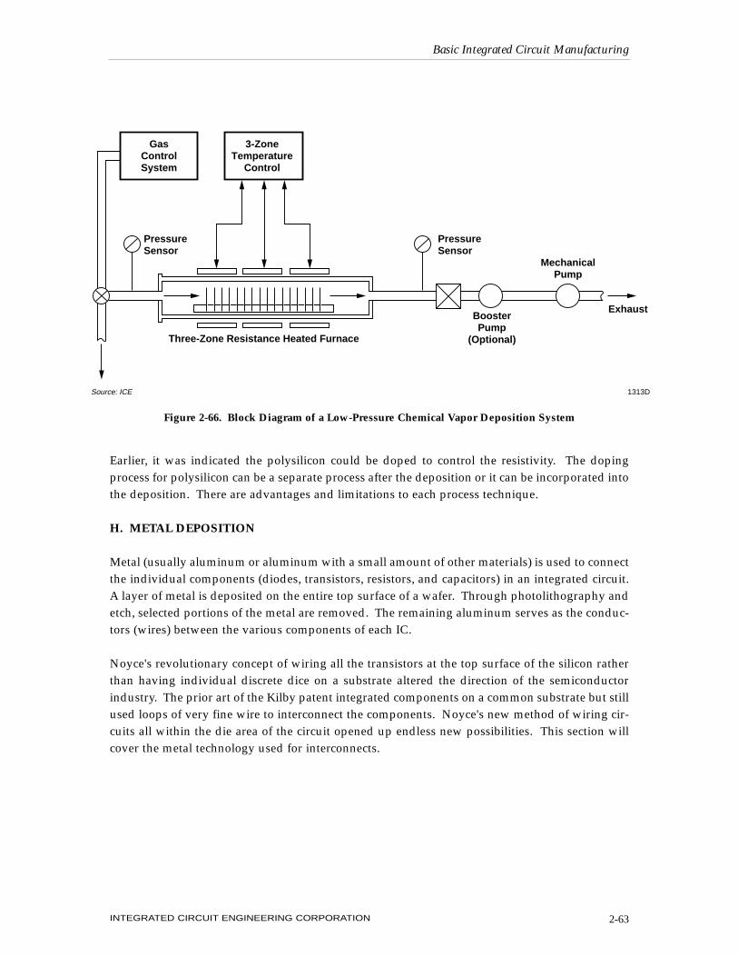
Earlier, it was indicated the polysilicon could be doped to control the resistivity. The dopingprocess for polysilicon can be a separate process after the deposition or it can be incorporated intothe deposition. There are advantages and limitations to each process technique.
H. METAL DEPOSITION
Metal (usually aluminum or aluminum with a small amount of other materials) is used to connectthe individual components (diodes, transistors, resistors, and capacitors) in an integrated circuit.A layer of metal is deposited on the entire top surface of a wafer. Through photolithography andetch, selected portions of the metal are removed. The remaining aluminum serves as the conduc-tors (wires) between the various components of each IC.
Noyce's revolutionary concept of wiring all the transistors at the top surface of the silicon ratherthan having individual discrete dice on a substrate altered the direction of the semiconductorindustry. The prior art of the Kilby patent integrated components on a common substrate but stillused loops of very fine wire to interconnect the components. Noyce's new method of wiring cir-cuits all within the die area of the circuit opened up endless new possibilities. This section willcover the metal technology used for interconnects.
Basic Integrated Circuit Manufacturing
INTEGRATED CIRCUIT ENGINEERING CORPORATION 2-63
GasControlSystem
3-ZoneTemperature
Control
PressureSensor
PressureSensor
Three-Zone Resistance Heated Furnace
BoosterPump
(Optional)
MechanicalPump
Exhaust
1313DSource: ICE
Figure 2-66. Block Diagram of a Low-Pressure Chemical Vapor Deposition System
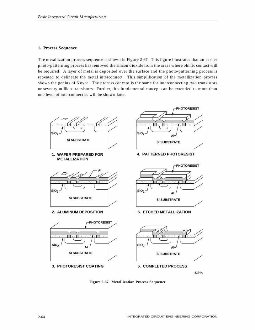
1. Process Sequence
The metallization process sequence is shown in Figure 2-67. This figure illustrates that an earlierphoto-patterning process has removed the silicon dioxide from the areas where ohmic contact willbe required. A layer of metal is deposited over the surface and the photo-patterning process isrepeated to delineate the metal interconnect. This simplification of the metallization processshows the genius of Noyce. The process concept is the same for interconnecting two transistorsor seventy million transistors. Further, this fundamental concept can be extended to more thanone level of interconnect as will be shown later.
Basic Integrated Circuit Manufacturing
INTEGRATED CIRCUIT ENGINEERING CORPORATION2-64
SiO2
Si SUBSTRATE
SiO2
Si SUBSTRATE
Al
SiO2
Si SUBSTRATE
Al
PHOTORESIST
1. WAFER PREPARED FOR METALLIZATION
2. ALUMINUM DEPOSITION
3. PHOTORESIST COATING
SiO2
Si SUBSTRATE
PHOTORESIST
Al
SiO2
Si SUBSTRATE
PHOTORESIST
Al
SiO2
Si SUBSTRATE
Al
4. PATTERNED PHOTORESIST
5. ETCHED METALLIZATION
6. COMPLETED PROCESS
8274A
Figure 2-67. Metallization Process Sequence
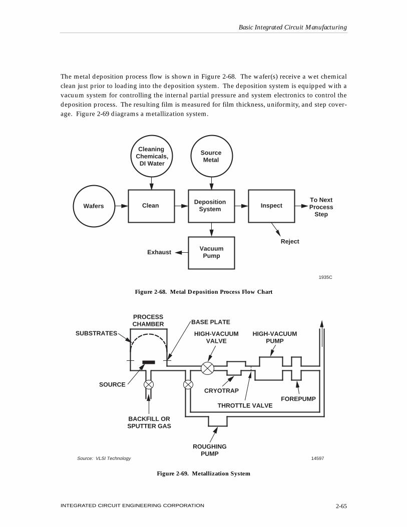
The metal deposition process flow is shown in Figure 2-68. The wafer(s) receive a wet chemicalclean just prior to loading into the deposition system. The deposition system is equipped with avacuum system for controlling the internal partial pressure and system electronics to control thedeposition process. The resulting film is measured for film thickness, uniformity, and step cover-age. Figure 2-69 diagrams a metallization system.
Basic Integrated Circuit Manufacturing
INTEGRATED CIRCUIT ENGINEERING CORPORATION 2-65
Cleaning Chemicals,
DI Water
SourceMetal
Wafers Clean DepositionSystem Inspect
To NextProcess
Step
Reject
Exhaust VacuumPump
1935C
Figure 2-68. Metal Deposition Process Flow Chart
PROCESSCHAMBER
SUBSTRATES
SOURCE
BASE PLATE
HIGH-VACUUMVALVE
BACKFILL ORSPUTTER GAS
ROUGHINGPUMP
CRYOTRAP
HIGH-VACUUMPUMP
FOREPUMPTHROTTLE VALVE
14597Source: VLSI Technology
Figure 2-69. Metallization System
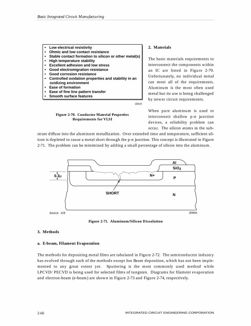
2. Materials
The basic materials requirements tointerconnect the components withinan IC are listed in Figure 2-70.Unfortunately, no individual metalcan meet all of the requirements.Aluminum is the most often usedmetal but its use is being challengedby newer circuit requirements.
When pure aluminum is used tointerconnect shallow p-n junctiondevices, a reliability problem canoccur. The silicon atoms in the sub-
strate diffuse into the aluminum metallization. Over extended time and temperature, sufficient sil-icon is depleted to cause a metal short through the p-n junction. This concept is illustrated in Figure2-71. The problem can be minimized by adding a small percentage of silicon into the aluminum.
3. Methods
a. E-beam, Filament Evaporation
The methods for depositing metal films are tabulated in Figure 2-72. The semiconductor industryhas evolved through each of the methods except Ion Beam deposition, which has not been imple-mented to any great extent yet. Sputtering is the most commonly used method whileLPCVD/PECVD is being used for selected films of tungsten. Diagrams for filament evaporationand electron-beam (e-beam) are shown in Figure 2-73 and Figure 2-74, respectively.
Basic Integrated Circuit Manufacturing
INTEGRATED CIRCUIT ENGINEERING CORPORATION2-66
18419
Figure 2-70. Conductor Material PropertiesRequirements for VLSI
• Low electrical resistivity• Ohmic and low contact resistance• Stable contact formation to silicon or other metal(s)• High temperature stability• Excellent adhesion and low stress• Good electromigration resistance• Good corrosion resistance• Controlled oxidation properties and stability in an oxidizing environment• Ease of formation• Ease of fine line pattern transfer• Smooth surface features
SHORT N
0.3µ PN+
AlSiO2
3090ASource: ICE
Figure 2-71. Aluminum/Silicon Dissolution
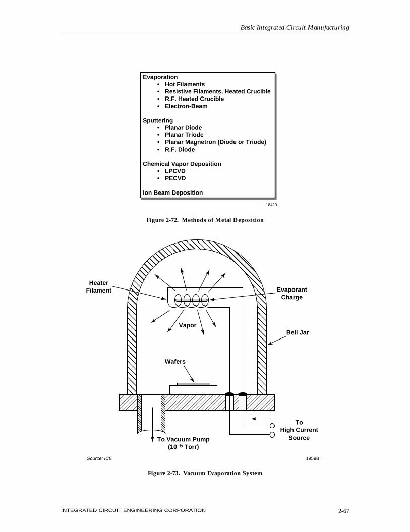
Basic Integrated Circuit Manufacturing
INTEGRATED CIRCUIT ENGINEERING CORPORATION 2-67
Evaporation• Hot Filaments• Resistive Filaments, Heated Crucible• R.F. Heated Crucible• Electron-Beam
Sputtering• Planar Diode• Planar Triode• Planar Magnetron (Diode or Triode)• R.F. Diode
Chemical Vapor Deposition• LPCVD• PECVD
Ion Beam Deposition
18420
Figure 2-72. Methods of Metal Deposition
@@@@@@@@@@@@
ÀÀÀÀÀÀÀÀÀÀÀÀ
@@@@@@@@@@@@
ÀÀÀÀÀÀÀÀÀÀÀÀ
@@@@@@@@@@@@
ÀÀÀÀÀÀÀÀÀÀÀÀ
@@@@@@@@@@@@
ÀÀÀÀÀÀÀÀÀÀÀÀ
@@@@@@@@@@@@
ÀÀÀÀÀÀÀÀÀÀÀÀ
@@@@@@@@@@@@
ÀÀÀÀÀÀÀÀÀÀÀÀ
Wafers
Vapor
HeaterFilament Evaporant
Charge
Bell Jar
To High Current
SourceTo Vacuum Pump(10–5 Torr)
1959BSource: ICE
Figure 2-73. Vacuum Evaporation System
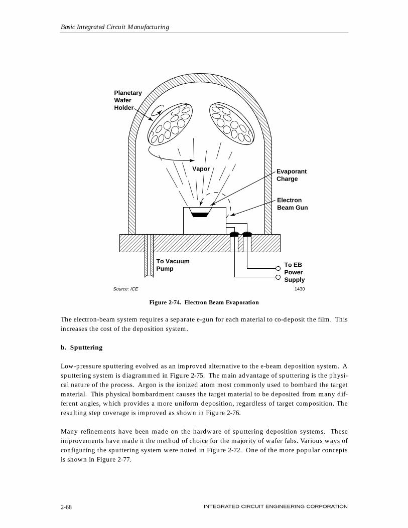
The electron-beam system requires a separate e-gun for each material to co-deposit the film. Thisincreases the cost of the deposition system.
b. Sputtering
Low-pressure sputtering evolved as an improved alternative to the e-beam deposition system. Asputtering system is diagrammed in Figure 2-75. The main advantage of sputtering is the physi-cal nature of the process. Argon is the ionized atom most commonly used to bombard the targetmaterial. This physical bombardment causes the target material to be deposited from many dif-ferent angles, which provides a more uniform deposition, regardless of target composition. Theresulting step coverage is improved as shown in Figure 2-76.
Many refinements have been made on the hardware of sputtering deposition systems. Theseimprovements have made it the method of choice for the majority of wafer fabs. Various ways ofconfiguring the sputtering system were noted in Figure 2-72. One of the more popular conceptsis shown in Figure 2-77.
Basic Integrated Circuit Manufacturing
INTEGRATED CIRCUIT ENGINEERING CORPORATION2-68
PlanetaryWaferHolder
EvaporantCharge
ElectronBeam Gun
To EBPowerSupply
To VacuumPump
Vapor
1430Source: ICE
Figure 2-74. Electron Beam Evaporation
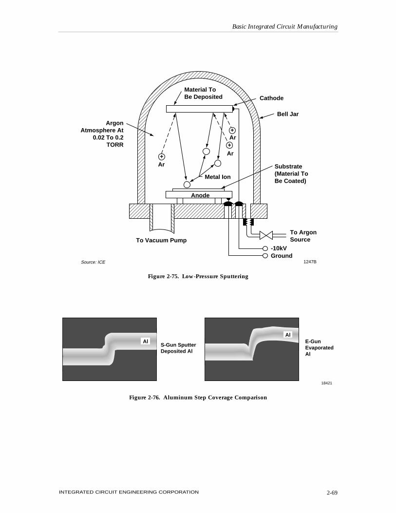
Basic Integrated Circuit Manufacturing
INTEGRATED CIRCUIT ENGINEERING CORPORATION 2-69
+
+
+
To Vacuum PumpTo ArgonSource
-10kVGround
Substrate(Material ToBe Coated)
Bell Jar
Cathode
ArgonAtmosphere At
0.02 To 0.2TORR
Anode
Metal Ion
Ar
Ar
Ar
Material ToBe Deposited
1247BSource: ICE
Figure 2-75. Low-Pressure Sputtering
AlS-Gun SputterDeposited Al
AlE-GunEvaporatedAl
18421
Figure 2-76. Aluminum Step Coverage Comparison
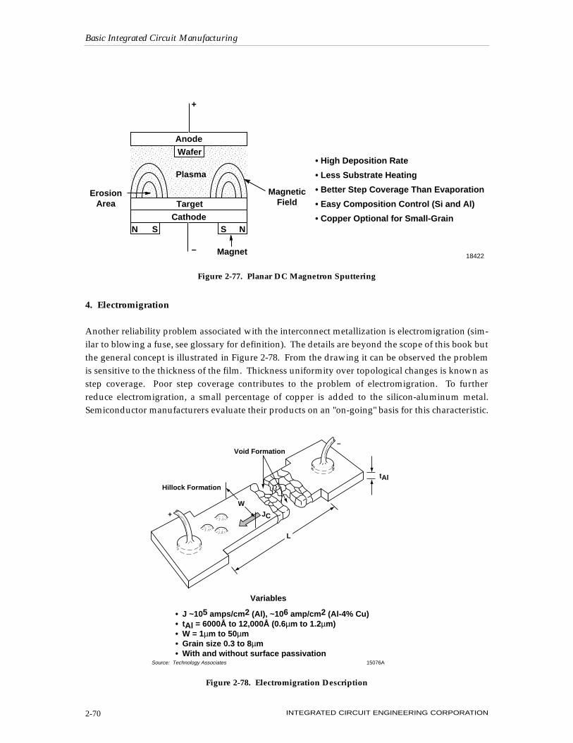
4. Electromigration
Another reliability problem associated with the interconnect metallization is electromigration (sim-ilar to blowing a fuse, see glossary for definition). The details are beyond the scope of this book butthe general concept is illustrated in Figure 2-78. From the drawing it can be observed the problemis sensitive to the thickness of the film. Thickness uniformity over topological changes is known asstep coverage. Poor step coverage contributes to the problem of electromigration. To furtherreduce electromigration, a small percentage of copper is added to the silicon-aluminum metal.Semiconductor manufacturers evaluate their products on an "on-going" basis for this characteristic.
Basic Integrated Circuit Manufacturing
INTEGRATED CIRCUIT ENGINEERING CORPORATION2-70
Anode
Plasma
ErosionArea
MagneticField
Magnet
Cathode
Target
–
+
18422
N S NS
• High Deposition Rate
• Less Substrate Heating
• Better Step Coverage Than Evaporation
• Easy Composition Control (Si and Al)
• Copper Optional for Small-Grain
Wafer
Figure 2-77. Planar DC Magnetron Sputtering
tAlHillock Formation
Void Formation
+
W
L
–
JC
• J ~105 amps/cm2 (Al), ~106 amp/cm2 (Al-4% Cu)• tAl = 6000Å to 12,000Å (0.6µm to 1.2µm)• W = 1µm to 50µm• Grain size 0.3 to 8µm• With and without surface passivation
Source: Technology Associates 15076A
Variables
Figure 2-78. Electromigration Description
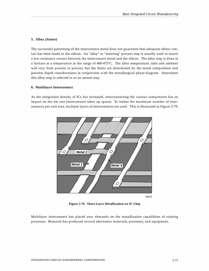
5. Alloy (Sinter)
The successful patterning of the interconnect metal does not guarantee that adequate ohmic con-tact has been made to the silicon. An "alloy" or "sintering" process step is usually used to insurea low-resistance contact between the interconnect metal and the silicon. The alloy step is done ina furnace at a temperature in the range of 400-475°C. The alloy temperature, time and ambientwill vary from process to process, but the limits are determined by the metal composition andjunction depth considerations in conjunction with the metallurgical phase-diagram. Sometimesthis alloy step is referred to as an anneal step.
6. Multilayer Interconnect
As the integration density of ICs has increased, interconnecting the various components has animpact on the die size (interconnect takes up space). To realize the maximum number of inter-connects per unit area, multiple layers of interconnects are used. This is illustrated in Figure 2-79.
Multilayer interconnect has placed new demands on the metallization capabilities of existingprocesses. Research has produced several alternative materials, processes, and equipment.
Basic Integrated Circuit Manufacturing
INTEGRATED CIRCUIT ENGINEERING CORPORATION 2-71
18415
Metal 1 Metal 3
Metal 2
Figure 2-79. Three-Layer Metallization on IC Chip
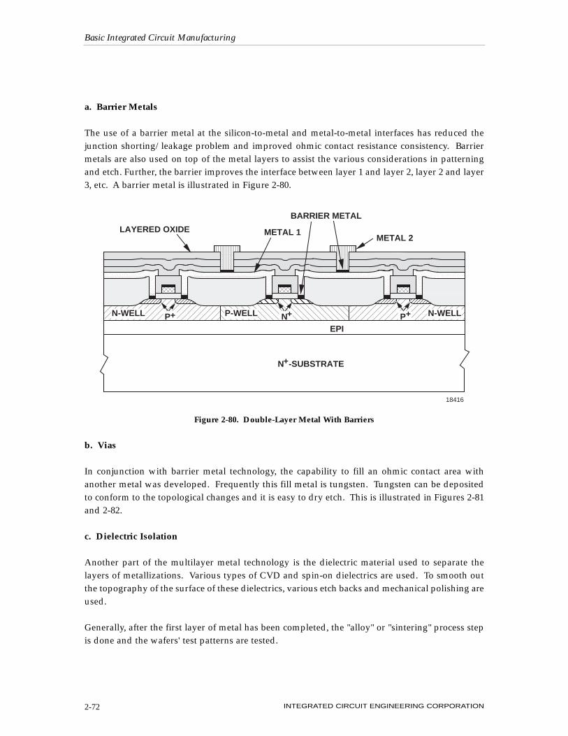
a. Barrier Metals
The use of a barrier metal at the silicon-to-metal and metal-to-metal interfaces has reduced thejunction shorting/leakage problem and improved ohmic contact resistance consistency. Barriermetals are also used on top of the metal layers to assist the various considerations in patterningand etch. Further, the barrier improves the interface between layer 1 and layer 2, layer 2 and layer3, etc. A barrier metal is illustrated in Figure 2-80.
b. Vias
In conjunction with barrier metal technology, the capability to fill an ohmic contact area withanother metal was developed. Frequently this fill metal is tungsten. Tungsten can be depositedto conform to the topological changes and it is easy to dry etch. This is illustrated in Figures 2-81and 2-82.
c. Dielectric Isolation
Another part of the multilayer metal technology is the dielectric material used to separate thelayers of metallizations. Various types of CVD and spin-on dielectrics are used. To smooth outthe topography of the surface of these dielectrics, various etch backs and mechanical polishing areused.
Generally, after the first layer of metal has been completed, the "alloy" or "sintering" process stepis done and the wafers' test patterns are tested.
Basic Integrated Circuit Manufacturing
INTEGRATED CIRCUIT ENGINEERING CORPORATION2-72
EPI
N -SUBSTRATE+
18416
N-WELL N-WELLP-WELL
+P +PN+
BARRIER METAL
METAL 2METAL 1LAYERED OXIDE
Figure 2-80. Double-Layer Metal With Barriers
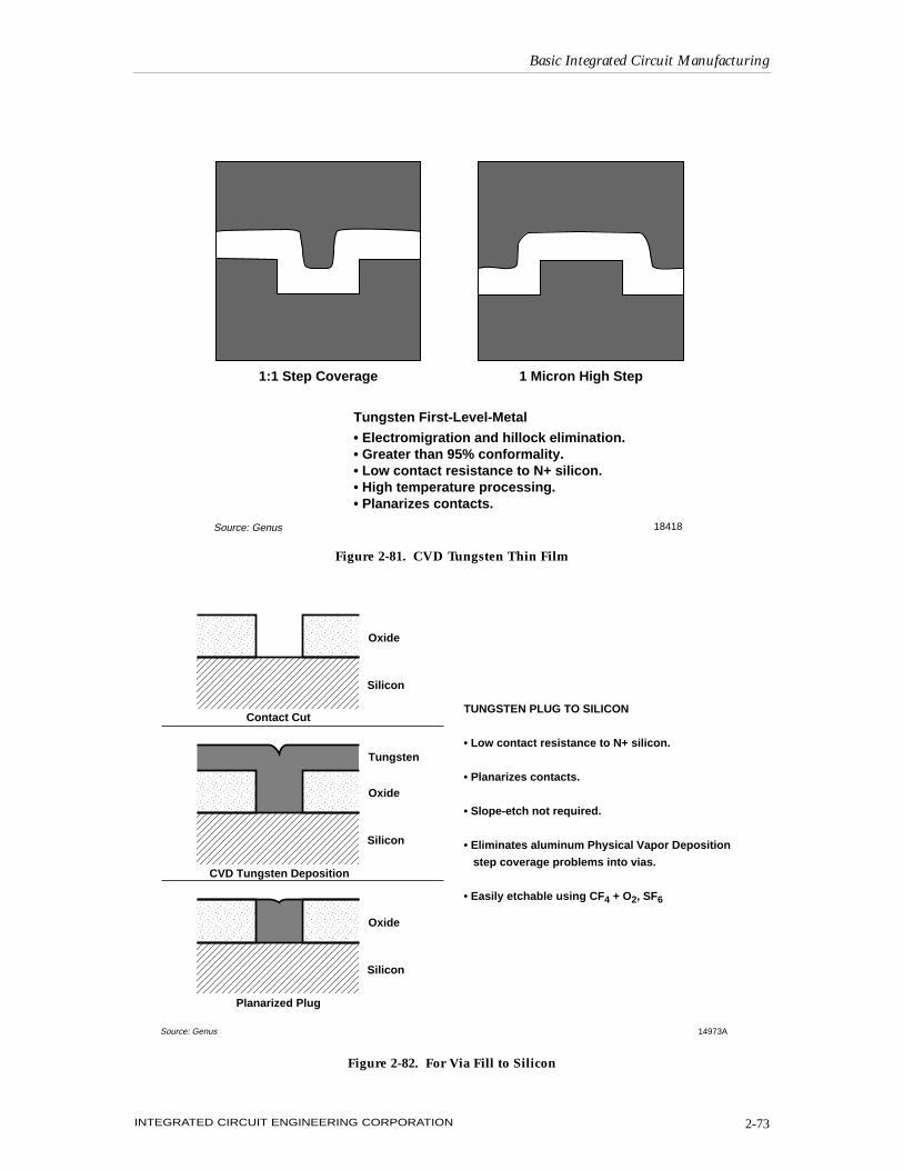
Basic Integrated Circuit Manufacturing
INTEGRATED CIRCUIT ENGINEERING CORPORATION 2-73
1:1 Step Coverage 1 Micron High Step
Tungsten First-Level-Metal
• Electromigration and hillock elimination.• Greater than 95% conformality.• Low contact resistance to N+ silicon.• High temperature processing.• Planarizes contacts.
18418Source: Genus
Figure 2-81. CVD Tungsten Thin Film
Oxide
Silicon
Oxide
Silicon
Oxide
Silicon
Contact Cut
Tungsten
CVD Tungsten Deposition
Planarized Plug
Source: Genus
TUNGSTEN PLUG TO SILICON
• Low contact resistance to N+ silicon.
• Planarizes contacts.
• Slope-etch not required.
• Eliminates aluminum Physical Vapor Deposition
step coverage problems into vias.
• Easily etchable using CF4 + O2, SF6
14973A
Figure 2-82. For Via Fill to Silicon
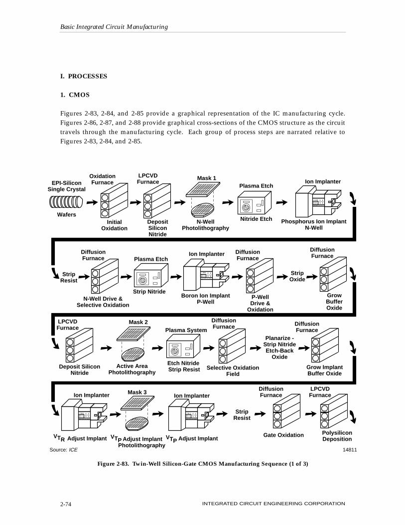
I. PROCESSES
1. CMOS
Figures 2-83, 2-84, and 2-85 provide a graphical representation of the IC manufacturing cycle.Figures 2-86, 2-87, and 2-88 provide graphical cross-sections of the CMOS structure as the circuittravels through the manufacturing cycle. Each group of process steps are narrated relative toFigures 2-83, 2-84, and 2-85.
Basic Integrated Circuit Manufacturing
INTEGRATED CIRCUIT ENGINEERING CORPORATION2-74
EPI-SiliconSingle Crystal
StripResist
14811Source: ICE
Wafers
Plasma Etch
InitialOxidation
DepositSiliconNitride
Ion Implanter
Plasma Etch
Nitride Etch
OxidationFurnace
LPCVDFurnace
Mask 1
N-WellPhotolithography
LPCVDFurnace
Deposit SiliconNitride
Phosphorus Ion ImplantN-Well
Ion Implanter
Strip NitrideBoron Ion Implant
P-Well
Active AreaPhotolithography
Mask 2Plasma System
Etch Nitride Strip Resist
DiffusionFurnace
DiffusionFurnace
Selective OxidationField
Planarize -Strip NitrideEtch-Back
Oxide
DiffusionFurnace
Grow ImplantBuffer Oxide
Ion Implanter
VTR VTPAdjust Implant VTP Adjust Implant
Mask 3Ion Implanter
DiffusionFurnace
LPCVDFurnace
Gate Oxidation PolysiliconDeposition
N-Well Drive &Selective Oxidation
P-WellDrive &
Oxidation
StripOxide
GrowBufferOxide
DiffusionFurnace
Adjust ImplantPhotolithography
DiffusionFurnace
StripResist
Figure 2-83. Twin-Well Silicon-Gate CMOS Manufacturing Sequence (1 of 3)
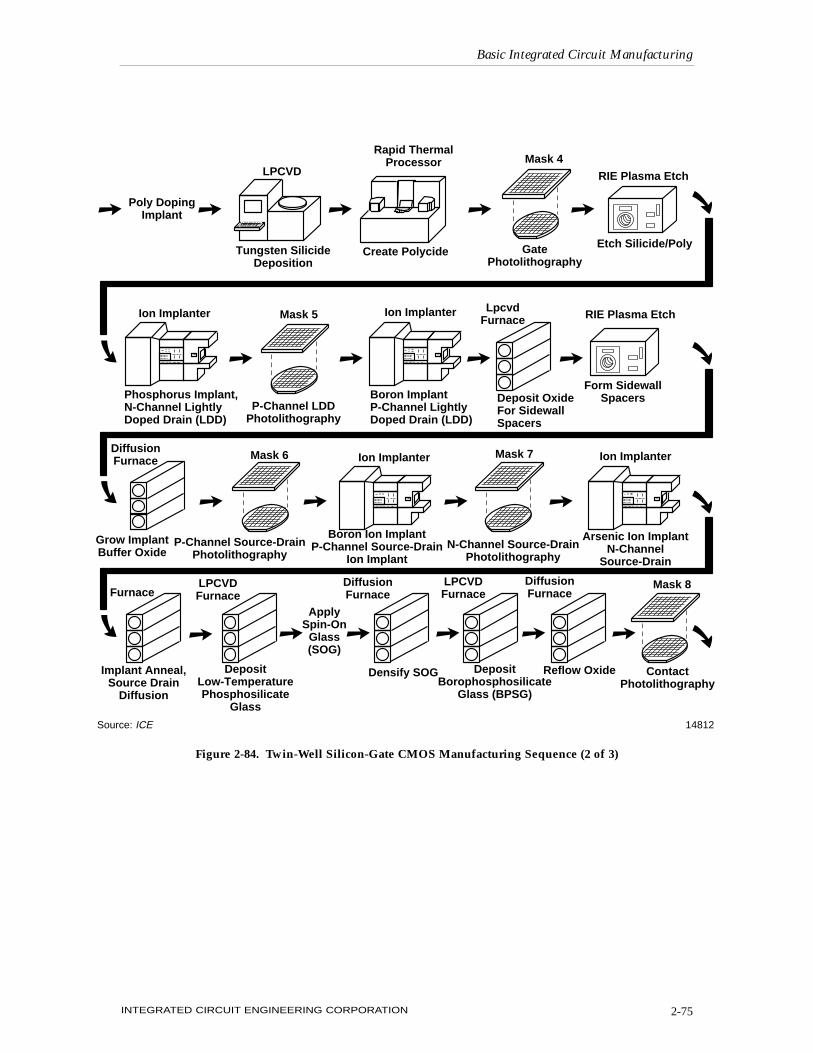
Basic Integrated Circuit Manufacturing
INTEGRATED CIRCUIT ENGINEERING CORPORATION 2-75
14812Source: ICE
Poly DopingImplant
LPCVD
Tungsten SilicideDeposition
Rapid ThermalProcessor
Create Polycide
Mask 4
GatePhotolithography
RIE Plasma Etch
Etch Silicide/Poly
Ion Implanter
Phosphorus Implant,N-Channel LightlyDoped Drain (LDD)
Mask 5
P-Channel LDDPhotolithography
Ion Implanter
Boron ImplantP-Channel LightlyDoped Drain (LDD)
LpcvdFurnace
Deposit OxideFor SidewallSpacers
RIE Plasma Etch
Form SidewallSpacers
DiffusionFurnace
Grow ImplantBuffer Oxide
P-Channel Source-DrainPhotolithography
Mask 6 Ion Implanter
Boron Ion ImplantP-Channel Source-Drain
Ion Implant
Mask 7
N-Channel Source-DrainPhotolithography
Ion Implanter
Arsenic Ion ImplantN-Channel
Source-Drain
Furnace
Implant Anneal,Source Drain
Diffusion
LPCVDFurnace
DepositLow-TemperaturePhosphosilicate
Glass
ApplySpin-On
Glass(SOG)
DiffusionFurnace
Densify SOG
LPCVDFurnace
DepositBorophosphosilicate
Glass (BPSG)
DiffusionFurnace
Reflow Oxide
Mask 8
ContactPhotolithography
Figure 2-84. Twin-Well Silicon-Gate CMOS Manufacturing Sequence (2 of 3)
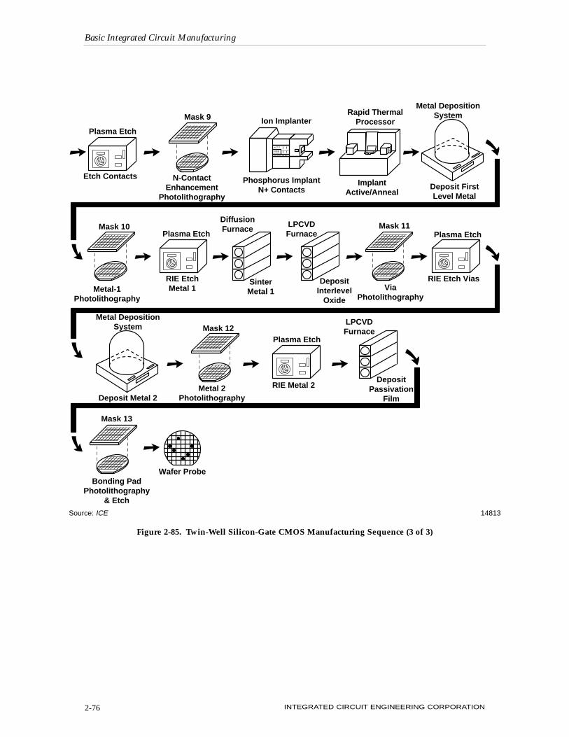
Basic Integrated Circuit Manufacturing
INTEGRATED CIRCUIT ENGINEERING CORPORATION2-76
14813Source: ICE
Rapid ThermalProcessor
Plasma Etch
Etch Contacts
Mask 9
N-ContactEnhancement
Photolithography
Ion Implanter
Phosphorus ImplantN+ Contacts
ImplantActive/Anneal
Metal DepositionSystem
Deposit FirstLevel Metal
Mask 10
Metal-1Photolithography
Plasma Etch
RIE EtchMetal 1
DiffusionFurnace
SinterMetal 1
LPCVDFurnace
DepositInterlevel
Oxide
Mask 11
ViaPhotolithography
Plasma Etch
RIE Etch Vias
Metal DepositionSystem
Deposit Metal 2
Mask 12
Metal 2 Photolithography
Plasma Etch
RIE Metal 2
LPCVDFurnace
DepositPassivation
Film
Mask 13
Wafer ProbeBonding Pad
Photolithography& Etch
Figure 2-85. Twin-Well Silicon-Gate CMOS Manufacturing Sequence (3 of 3)
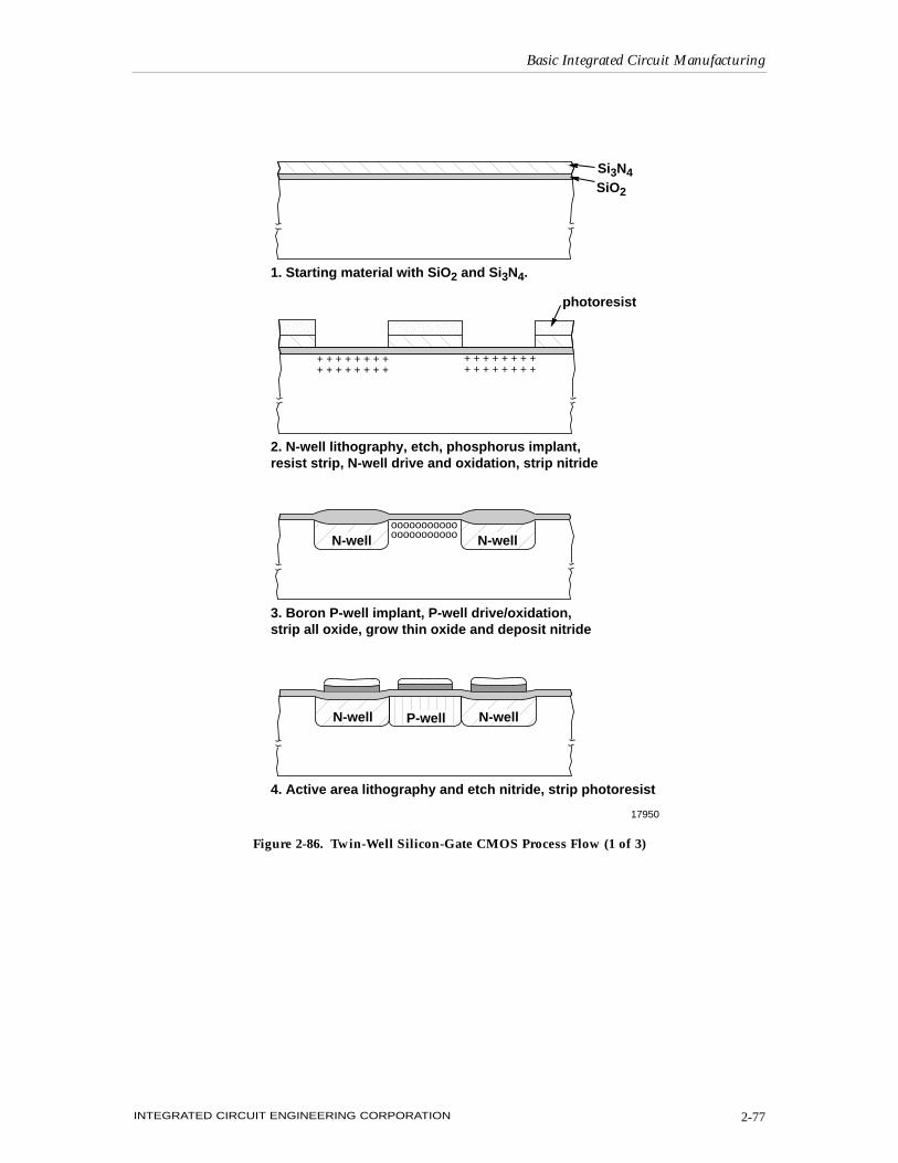
Basic Integrated Circuit Manufacturing
INTEGRATED CIRCUIT ENGINEERING CORPORATION 2-77
+ + + + + + + ++ + + + + + + +
+ + + + + + + ++ + + + + + + +
ooooooooooo
ooooooooooo
1. Starting material with SiO2 and Si3N4.
2. N-well lithography, etch, phosphorus implant, resist strip, N-well drive and oxidation, strip nitride
3. Boron P-well implant, P-well drive/oxidation, strip all oxide, grow thin oxide and deposit nitride
4. Active area lithography and etch nitride, strip photoresist
Si3N4SiO2
photoresist
17950
N-well N-well
N-well N-wellP-well
Figure 2-86. Twin-Well Silicon-Gate CMOS Process Flow (1 of 3)
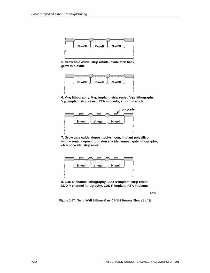
Basic Integrated Circuit Manufacturing
INTEGRATED CIRCUIT ENGINEERING CORPORATION2-78
+ + + + + + + + + + + + + + + + +
++++++++++++++++++++++++ +++++
5. Grow field oxide, strip nitride, oxide etch back, grow thin oxide
6. VTN lithography, VTN implant, strip resist, VTP lithography, VTP implant strip resist, RTA implants, strip thin oxide
7. Grow gate oxide, deposit polysilicon, implant polysilicon with arsenic, deposit tungsten silicide, anneal, gate lithography, etch polycide, strip resist
8. LDD N-channel lithography, LDD N-implant, strip resist, LDD P-channel lithography, LDD P-implant, RTA implants
polycide
17951
N-well N-wellP-well
N-well N-wellP-well
+ + + + + + + + +
N-well N-wellP-well
N-well N-wellP-well
Figure 2-87. Twin-Well Silicon-Gate CMOS Process Flow (2 of 3)
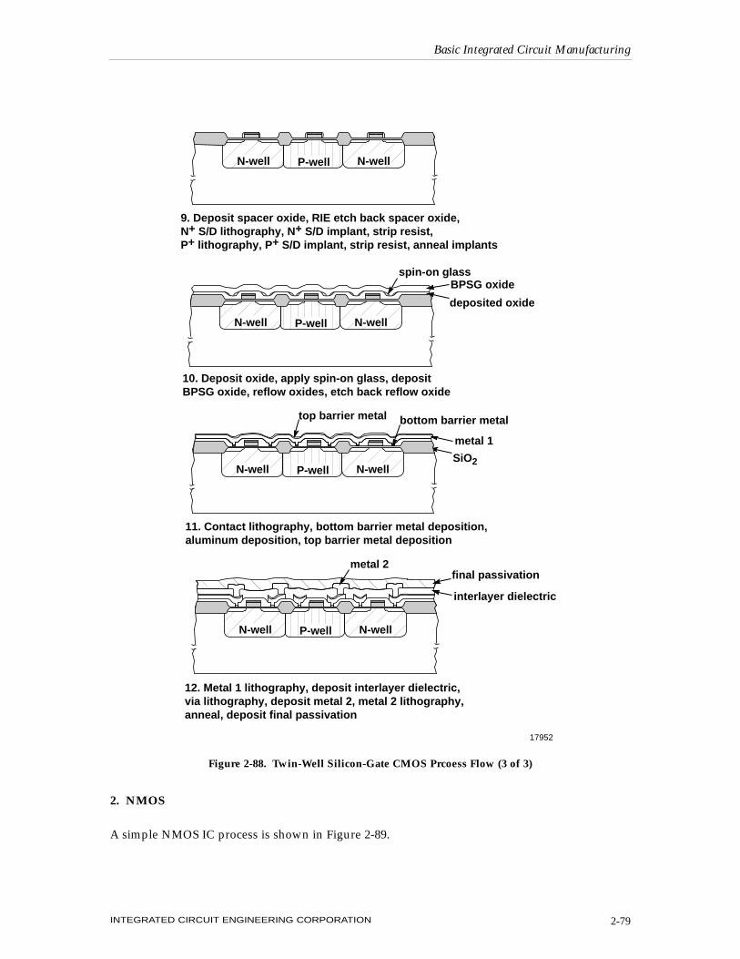
2. NMOS
A simple NMOS IC process is shown in Figure 2-89.
Basic Integrated Circuit Manufacturing
INTEGRATED CIRCUIT ENGINEERING CORPORATION 2-79
9. Deposit spacer oxide, RIE etch back spacer oxide,N+ S/D lithography, N+ S/D implant, strip resist, P+ lithography, P+ S/D implant, strip resist, anneal implants
10. Deposit oxide, apply spin-on glass, deposit BPSG oxide, reflow oxides, etch back reflow oxide
11. Contact lithography, bottom barrier metal deposition, aluminum deposition, top barrier metal deposition
12. Metal 1 lithography, deposit interlayer dielectric, via lithography, deposit metal 2, metal 2 lithography, anneal, deposit final passivation
final passivationmetal 2
interlayer dielectric
bottom barrier metaltop barrier metal
metal 1
SiO2
BPSG oxidespin-on glass
deposited oxide
17952
N-well N-wellP-well
N-well N-wellP-well
N-well N-wellP-well
N-well N-wellP-well
Figure 2-88. Twin-Well Silicon-Gate CMOS Prcoess Flow (3 of 3)
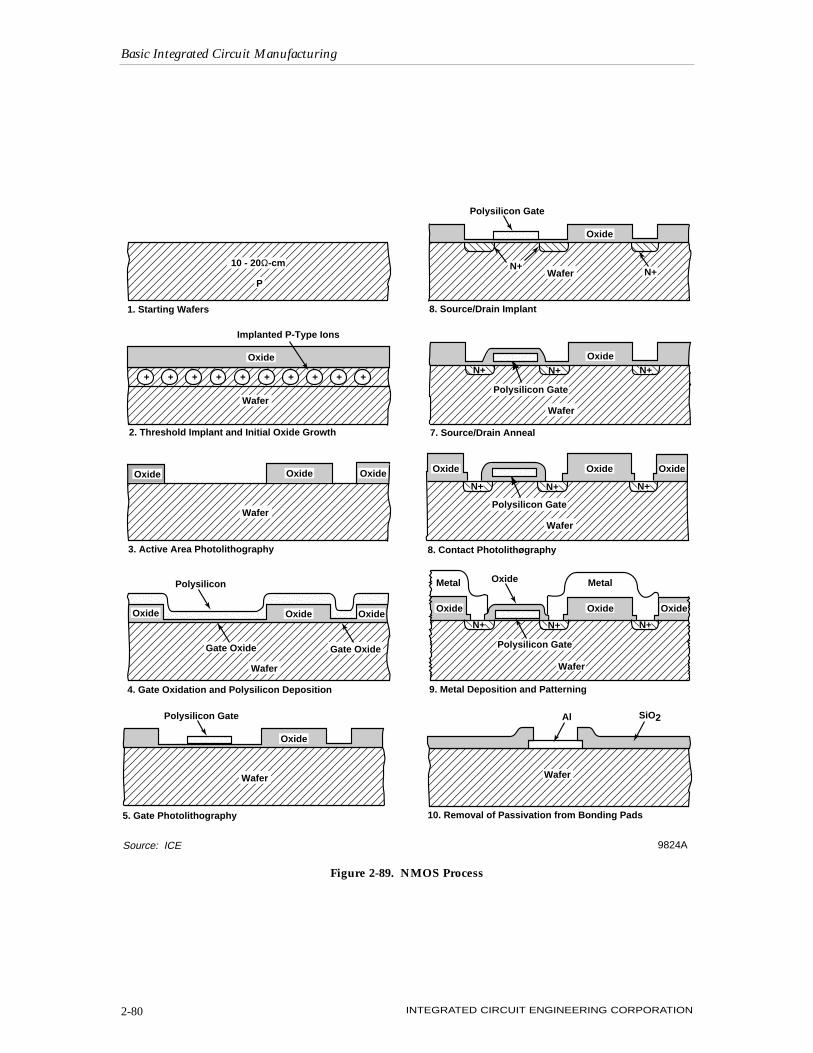
Basic Integrated Circuit Manufacturing
INTEGRATED CIRCUIT ENGINEERING CORPORATION2-80
Oxide
OxideOxideOxide
Metal Metal
Polysilicon Gate
Wafer
N+ N+ N+
Polysilicon Gate
Oxide
Wafer
N+ N+ N+
OxideOxide Oxide
Polysilicon Gate
Wafer
N+ N+ N+
Oxide
Wafer
Polysilicon Gate
Oxide
Wafer
Polysilicon Gate
N+N+
Oxide Oxide Oxide
Wafer
10 - 20Ω-cm
Wafer
Oxide Oxide Oxide
Wafer
Gate OxideGate Oxide
Polysilicon
9824ASource: ICE
Wafer
Oxide
+ + + + + + + + + +
Implanted P-Type Ions
P
1. Starting Wafers
2. Threshold Implant and Initial Oxide Growth
3. Active Area Photolithography
4. Gate Oxidation and Polysilicon Deposition
5. Gate Photolithography
9. Metal Deposition and Patterning
8. Contact Photolithøgraphy
7. Source/Drain Anneal
8. Source/Drain Implant
10. Removal of Passivation from Bonding Pads
Al SiO2
Figure 2-89. NMOS Process
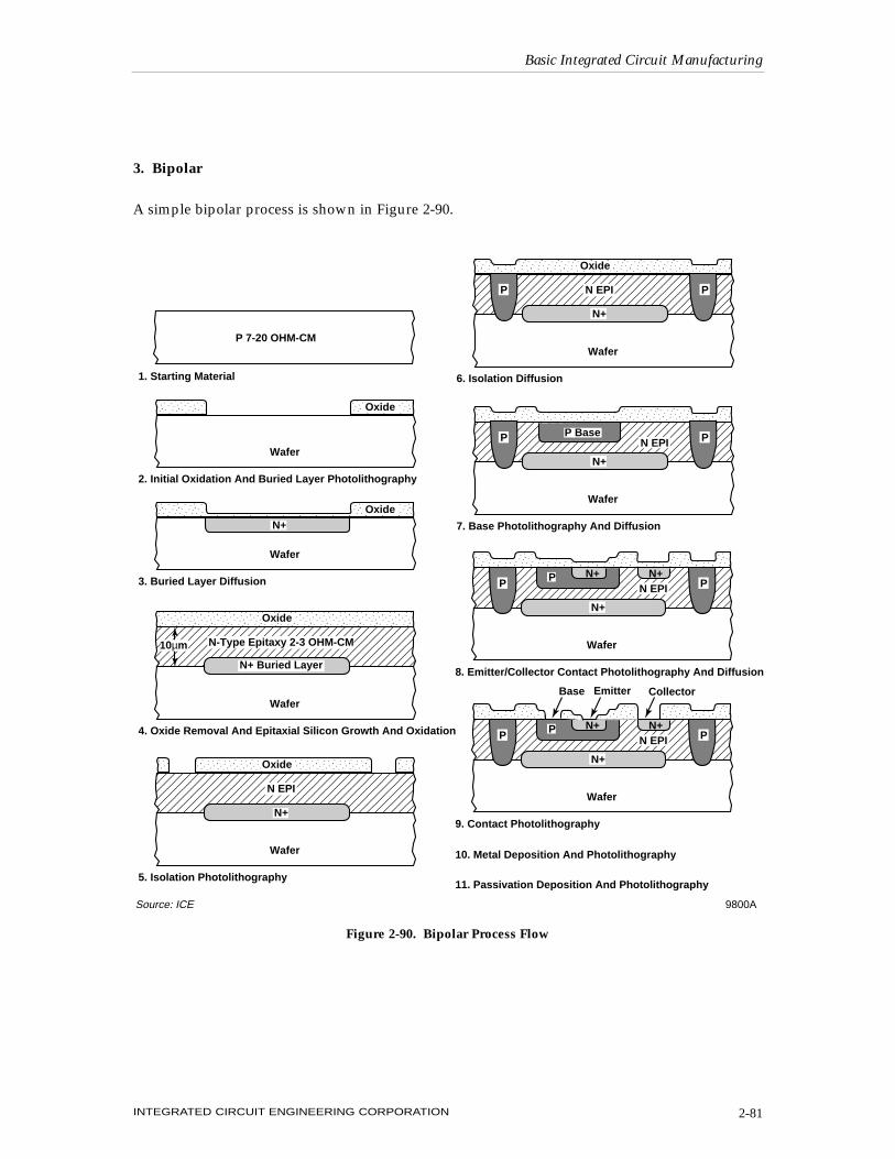
3. Bipolar
A simple bipolar process is shown in Figure 2-90.
Basic Integrated Circuit Manufacturing
INTEGRATED CIRCUIT ENGINEERING CORPORATION 2-81
1. Starting Material
2. Initial Oxidation And Buried Layer Photolithography
P 7-20 OHM-CM
Wafer
Oxide
3. Buried Layer Diffusion
Wafer
OxideN+
4. Oxide Removal And Epitaxial Silicon Growth And Oxidation
Wafer
Oxide
N+ Buried Layer
N-Type Epitaxy 2-3 OHM-CM10µm
6. Isolation Diffusion
Wafer
N+
N EPI
5. Isolation Photolithography
Wafer
Oxide
N+
N EPI
P
7. Base Photolithography And Diffusion
Wafer
N+
N EPI
Oxide
P Base
8. Emitter/Collector Contact Photolithography And Diffusion
Wafer
N+
N EPIP
9. Contact Photolithography
10. Metal Deposition And Photolithography
11. Passivation Deposition And Photolithography
Wafer
N+
N EPIP
Base Emitter Collector
N+ N+
N+ N+
9800ASource: ICE
P
P P
P P
P P
Figure 2-90. Bipolar Process Flow
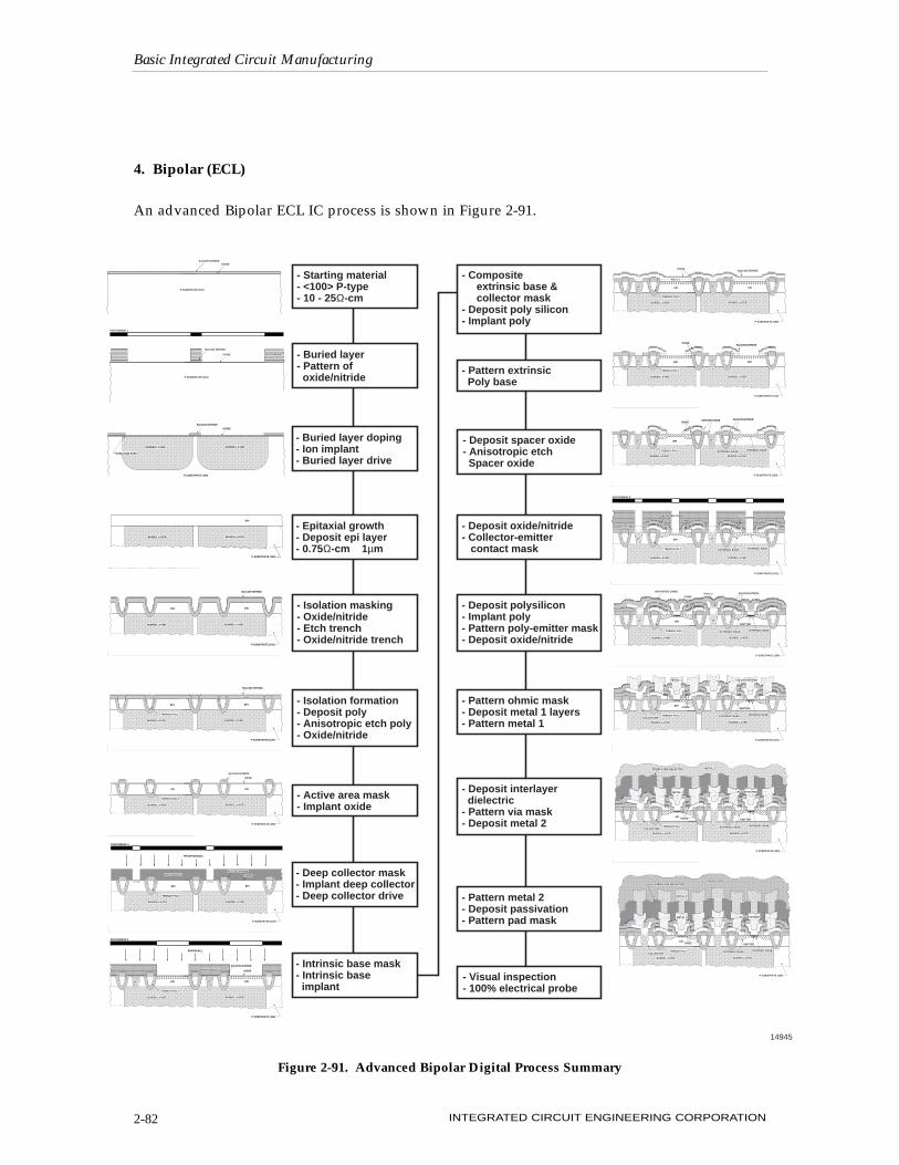
4. Bipolar (ECL)
An advanced Bipolar ECL IC process is shown in Figure 2-91.
Basic Integrated Circuit Manufacturing
INTEGRATED CIRCUIT ENGINEERING CORPORATION2-82
- Starting material - <100> P-type- 10 - 25Ω-cm
- Buried layer- Pattern of oxide/nitride
- Buried layer doping - Ion implant- Buried layer drive
- Epitaxial growth- Deposit epi layer- 0.75Ω-cm 1µm
- Isolation masking - Oxide/nitride- Etch trench- Oxide/nitride trench
- Isolation formation- Deposit poly- Anisotropic etch poly- Oxide/nitride
- Active area mask- Implant oxide
- Deep collector mask- Implant deep collector- Deep collector drive
- Intrinsic base mask- Intrinsic base implant
- Composite extrinsic base & collector mask- Deposit poly silicon- Implant poly
- Pattern extrinsic Poly base
- Deposit spacer oxide- Anisotropic etch Spacer oxide
- Deposit oxide/nitride- Collector-emitter contact mask
- Deposit polysilicon- Implant poly- Pattern poly-emitter mask- Deposit oxide/nitride
- Pattern ohmic mask- Deposit metal 1 layers- Pattern metal 1
- Deposit interlayer dielectric- Pattern via mask- Deposit metal 2
- Pattern metal 2- Deposit passivation- Pattern pad mask
- Visual inspection - 100% electrical probe
14945
PASSIVATION
METAL 2
BURIED LAYER
EPI
BURIED LAYER
P SUBSTRATE (100)
EXTRINSIC BASE INTRINSIC BASE
EMITTER
COLLECTOR
METAL 1
OXIDE
SILICON NITRIDE
INTERLAYER DIELECTRIC
TRENCH POLY
BURIED LAYER
EPI
BURIED LAYER
P SUBSTRATE (100)
EXTRINSIC BASE INTRINSIC BASE
EMITTER
COLLECTOR
METAL 1
OXIDE
SILICON NITRIDE
INTERLAYER DIELECTRIC METAL 2
TRENCH POLY
BURIED LAYER
EPI
BURIED LAYER
P SUBSTRATE (100)
EXTRINSIC BASE INTRINSIC BASE
EMITTER
COLLECTOR
METAL 1
OXIDE
SILICON NITRIDE
TRENCH POLY
BURIED LAYER
EPI
BURIED LAYER
P SUBSTRATE (100)
N+N+
SILICON NITRIDE
DEPOSITED OXIDE
POLY 2OXIDE
EXTRINSIC BASE INTRINSIC BASE
EMITTER
TRENCH POLY
BURIED LAYER
EPI
BURIED LAYER
P SUBSTRATE (100)
N+N+
SILICON NITRIDE
OXIDE
DEPOSITED OXIDE
EXTRINSIC BASE INTRINSIC BASETRENCH POLY
PHOTOMASK 8
BURIED LAYER
EPI
BURIED LAYER
P SUBSTRATE (100)
N+
SILICON NITRIDE
OXIDE
EXTRINSIC BASE INTRINSIC BASE
SPACER OXIDE
N+
TRENCH POLY
BURIED LAYER
EPI
EPI
BURIED LAYER
P SUBSTRATE (100)
N+N+
OXIDE
POLY 1
SILICON NITRIDE
TRENCH POLY
+ + + + + + + + + + + + + + ++ + + + + + + + + + + + + + +
+ + + + + + + + + + + + + + ++ + + + + + + + + + + + + + +
BURIED LAYER
EPI
EPI
BURIED LAYER
P SUBSTRATE (100)
N+N+
SILICON NITRIDE
+ + + + + + + + + + + + + + ++ + + + + + + + + + + + + + +
+ + + + + + + + + + + + + + ++ + + + + + + + + + + + + + +
OXIDE
POLY 1
TRENCH POLY
BURIED LAYER
EPI
OXIDE
EPI
BURIED LAYER
P SUBSTRATE (100)
SILICON NITRIDE
PHOTORESIST
+ + + + + + + + + + + + + + +
+ + + + + + + + + + + + + + ++ + + + + + + + + + + + + + ++ + + + + + + + + + + + + + +
N+N+
BORON BF2
TRENCH POLY
PHOTOMASK 5
BURIED LAYER
EPI
OXIDE
EPI
BURIED LAYER
P SUBSTRATE (100)
SILICON NITRIDEPHOTORESIST
PHOSPHOROUS
TRENCH POLY
PHOTOMASK 4
BURIED LAYER
EPI
OXIDE
EPI
BURIED LAYER
P SUBSTRATE (100)
SILICON NITRIDE
TRENCH POLY
BURIED LAYER
EPI
OXIDE
EPI
BURIED LAYER
P SUBSTRATE (100)
SILICON NITRIDE
TRENCH POLY
EPI
SILICON NITRIDE
OXIDE
EPI
BURIED LAYERBURIED LAYER
P SUBSTRATE (100)
P SUBSTRATE (100)
EPI
BURIED LAYERBURIED LAYER
P SUBSTRATE (100)
P SUBSTRATE (100)
BURIED LAYERBURIED LAYER
SILICON NITRIDE
OXIDE
OXIDATION STEP
P SUBSTRATE (100)
SILICON NITRIDE
OXIDE
PHOTORESIST
PHOTOMASK 1
P SUBSTRATE (100)
SILICON NITRIDEOXIDE
Figure 2-91. Advanced Bipolar Digital Process Summary
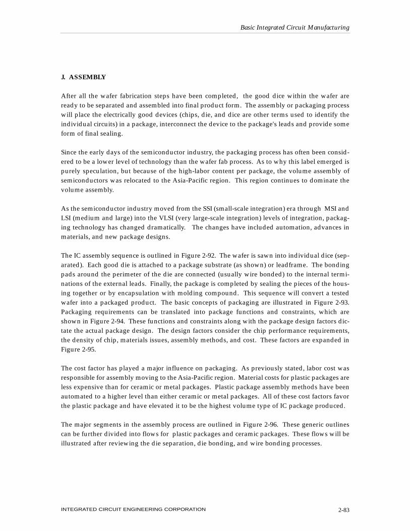
J. ASSEMBLY
After all the wafer fabrication steps have been completed, the good dice within the wafer areready to be separated and assembled into final product form. The assembly or packaging processwill place the electrically good devices (chips, die, and dice are other terms used to identify theindividual circuits) in a package, interconnect the device to the package's leads and provide someform of final sealing.
Since the early days of the semiconductor industry, the packaging process has often been consid-ered to be a lower level of technology than the wafer fab process. As to why this label emerged ispurely speculation, but because of the high-labor content per package, the volume assembly ofsemiconductors was relocated to the Asia-Pacific region. This region continues to dominate thevolume assembly.
As the semiconductor industry moved from the SSI (small-scale integration) era through MSI andLSI (medium and large) into the VLSI (very large-scale integration) levels of integration, packag-ing technology has changed dramatically. The changes have included automation, advances inmaterials, and new package designs.
The IC assembly sequence is outlined in Figure 2-92. The wafer is sawn into individual dice (sep-arated). Each good die is attached to a package substrate (as shown) or leadframe. The bondingpads around the perimeter of the die are connected (usually wire bonded) to the internal termi-nations of the external leads. Finally, the package is completed by sealing the pieces of the hous-ing together or by encapsulation with molding compound. This sequence will convert a testedwafer into a packaged product. The basic concepts of packaging are illustrated in Figure 2-93.Packaging requirements can be translated into package functions and constraints, which areshown in Figure 2-94. These functions and constraints along with the package design factors dic-tate the actual package design. The design factors consider the chip performance requirements,the density of chip, materials issues, assembly methods, and cost. These factors are expanded inFigure 2-95.
The cost factor has played a major influence on packaging. As previously stated, labor cost wasresponsible for assembly moving to the Asia-Pacific region. Material costs for plastic packages areless expensive than for ceramic or metal packages. Plastic package assembly methods have beenautomated to a higher level than either ceramic or metal packages. All of these cost factors favorthe plastic package and have elevated it to be the highest volume type of IC package produced.
The major segments in the assembly process are outlined in Figure 2-96. These generic outlinescan be further divided into flows for plastic packages and ceramic packages. These flows will beillustrated after reviewing the die separation, die bonding, and wire bonding processes.
Basic Integrated Circuit Manufacturing
INTEGRATED CIRCUIT ENGINEERING CORPORATION 2-83
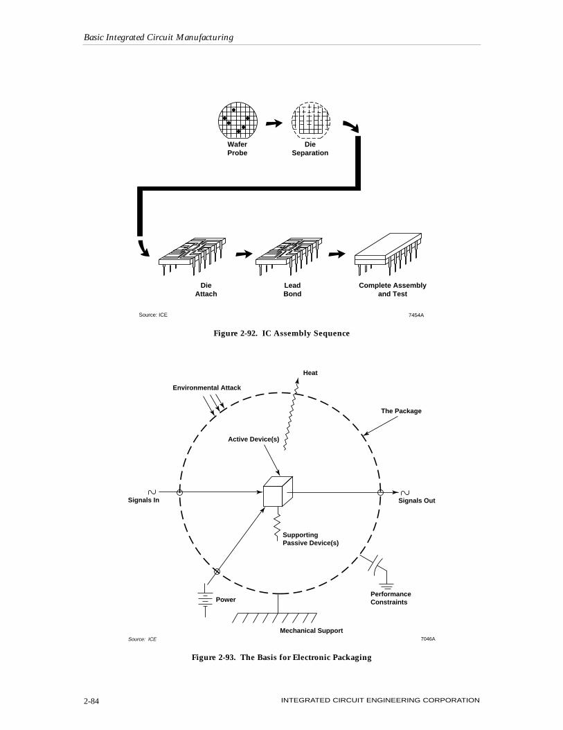
Basic Integrated Circuit Manufacturing
INTEGRATED CIRCUIT ENGINEERING CORPORATION2-84
WaferProbe
DieAttach
LeadBond
Complete Assemblyand Test
DieSeparation
7454ASource: ICE
Figure 2-92. IC Assembly Sequence
Environmental Attack
Signals In
Power
Mechanical Support
PerformanceConstraints
Signals Out
The Package
Heat
Active Device(s)
SupportingPassive Device(s)
7046ASource: ICE
Figure 2-93. The Basis for Electronic Packaging
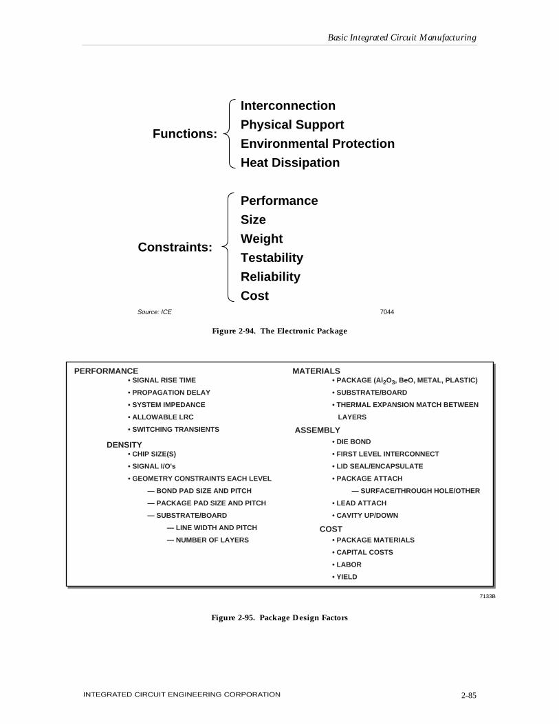
Basic Integrated Circuit Manufacturing
INTEGRATED CIRCUIT ENGINEERING CORPORATION 2-85
Interconnection
Physical Support
Environmental Protection
Heat Dissipation
Performance
Size
Weight
Testability
Reliability
Cost
Functions:
Constraints:
7044Source: ICE
Figure 2-94. The Electronic Package
Figure 2-95. Package Design Factors
• PACKAGE (Al2O3, BeO, METAL, PLASTIC)
• SUBSTRATE/BOARD
• THERMAL EXPANSION MATCH BETWEEN
LAYERS
• DIE BOND
• FIRST LEVEL INTERCONNECT
• LID SEAL/ENCAPSULATE
• PACKAGE ATTACH
— SURFACE/THROUGH HOLE/OTHER
• LEAD ATTACH
• CAVITY UP/DOWN
• PACKAGE MATERIALS
• CAPITAL COSTS
• LABOR
• YIELD
• SIGNAL RISE TIME
• PROPAGATION DELAY
• SYSTEM IMPEDANCE
• ALLOWABLE LRC
• SWITCHING TRANSIENTS
• CHIP SIZE(S)
• SIGNAL I/O's
• GEOMETRY CONSTRAINTS EACH LEVEL
— BOND PAD SIZE AND PITCH
— PACKAGE PAD SIZE AND PITCH
— SUBSTRATE/BOARD
— LINE WIDTH AND PITCH
— NUMBER OF LAYERS
PERFORMANCE
DENSITY
MATERIALS
ASSEMBLY
COST
7133B
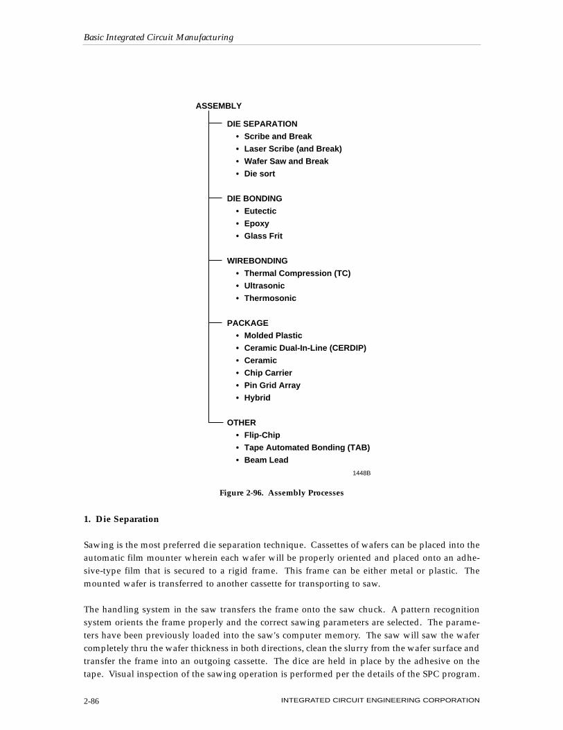
1. Die Separation
Sawing is the most preferred die separation technique. Cassettes of wafers can be placed into theautomatic film mounter wherein each wafer will be properly oriented and placed onto an adhe-sive-type film that is secured to a rigid frame. This frame can be either metal or plastic. Themounted wafer is transferred to another cassette for transporting to saw.
The handling system in the saw transfers the frame onto the saw chuck. A pattern recognitionsystem orients the frame properly and the correct sawing parameters are selected. The parame-ters have been previously loaded into the saw's computer memory. The saw will saw the wafercompletely thru the wafer thickness in both directions, clean the slurry from the wafer surface andtransfer the frame into an outgoing cassette. The dice are held in place by the adhesive on thetape. Visual inspection of the sawing operation is performed per the details of the SPC program.
Basic Integrated Circuit Manufacturing
INTEGRATED CIRCUIT ENGINEERING CORPORATION2-86
DIE SEPARATION
• Scribe and Break
• Laser Scribe (and Break)
• Wafer Saw and Break
• Die sort
DIE BONDING
• Eutectic
• Epoxy
• Glass Frit
WIREBONDING
• Thermal Compression (TC)
• Ultrasonic
• Thermosonic
PACKAGE
• Molded Plastic
• Ceramic Dual-In-Line (CERDIP)
• Ceramic
• Chip Carrier
• Pin Grid Array
• Hybrid
OTHER
• Flip-Chip
• Tape Automated Bonding (TAB)
• Beam Lead
ASSEMBLY
1448B
Figure 2-96. Assembly Processes
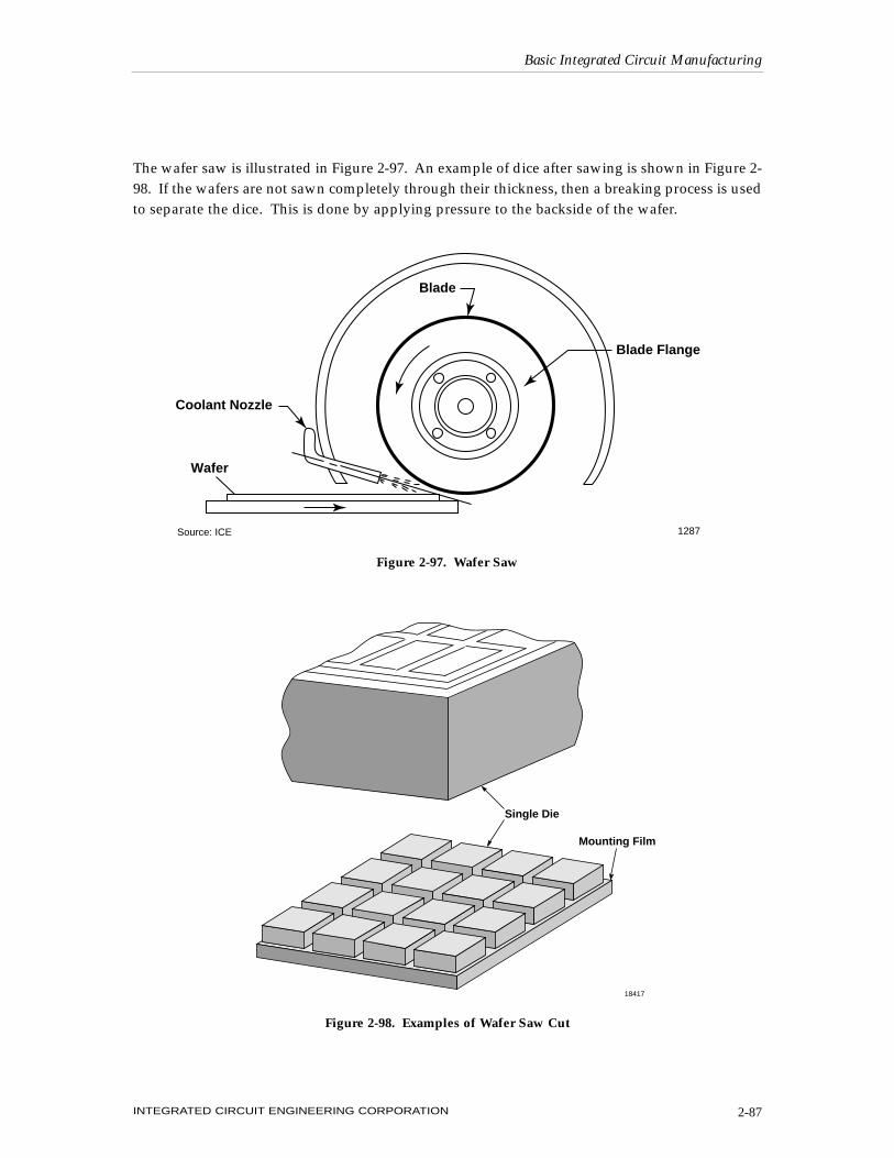
The wafer saw is illustrated in Figure 2-97. An example of dice after sawing is shown in Figure 2-98. If the wafers are not sawn completely through their thickness, then a breaking process is usedto separate the dice. This is done by applying pressure to the backside of the wafer.
Basic Integrated Circuit Manufacturing
INTEGRATED CIRCUIT ENGINEERING CORPORATION 2-87
Blade
Blade Flange
Coolant Nozzle
Wafer
1287Source: ICE
Figure 2-97. Wafer Saw
18417
Single Die
Mounting Film
Figure 2-98. Examples of Wafer Saw Cut
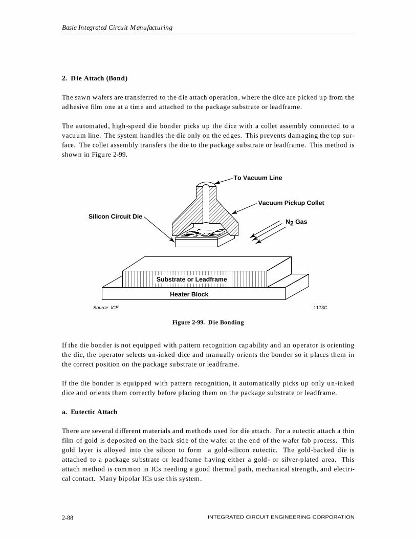
2. Die Attach (Bond)
The sawn wafers are transferred to the die attach operation, where the dice are picked up from theadhesive film one at a time and attached to the package substrate or leadframe.
The automated, high-speed die bonder picks up the dice with a collet assembly connected to avacuum line. The system handles the die only on the edges. This prevents damaging the top sur-face. The collet assembly transfers the die to the package substrate or leadframe. This method isshown in Figure 2-99.
If the die bonder is not equipped with pattern recognition capability and an operator is orientingthe die, the operator selects un-inked dice and manually orients the bonder so it places them inthe correct position on the package substrate or leadframe.
If the die bonder is equipped with pattern recognition, it automatically picks up only un-inkeddice and orients them correctly before placing them on the package substrate or leadframe.
a. Eutectic Attach
There are several different materials and methods used for die attach. For a eutectic attach a thinfilm of gold is deposited on the back side of the wafer at the end of the wafer fab process. Thisgold layer is alloyed into the silicon to form a gold-silicon eutectic. The gold-backed die isattached to a package substrate or leadframe having either a gold- or silver-plated area. Thisattach method is common in ICs needing a good thermal path, mechanical strength, and electri-cal contact. Many bipolar ICs use this system.
Basic Integrated Circuit Manufacturing
INTEGRATED CIRCUIT ENGINEERING CORPORATION2-88
Substrate or Leadframe
Silicon Circuit Die
To Vacuum Line
Vacuum Pickup Collet
N2 Gas
Heater Block
1173CSource: ICE
Figure 2-99. Die Bonding
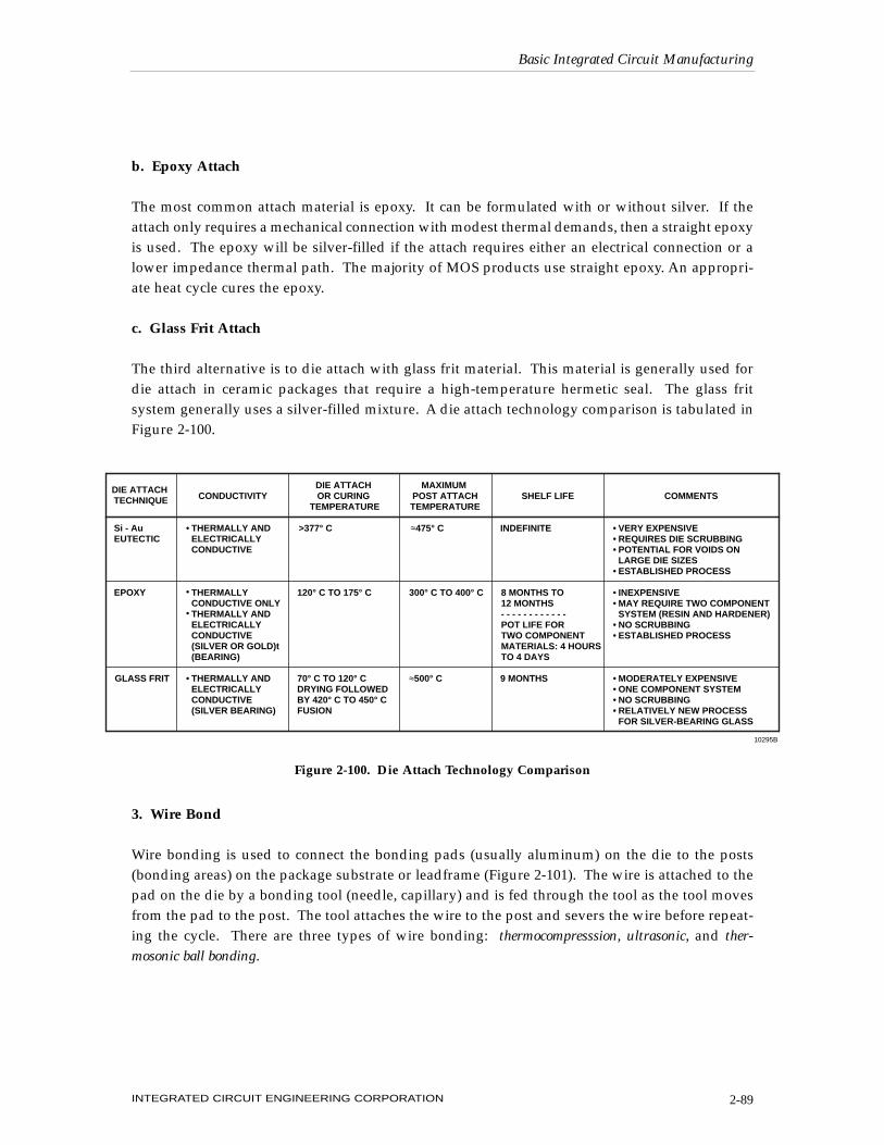
b. Epoxy Attach
The most common attach material is epoxy. It can be formulated with or without silver. If theattach only requires a mechanical connection with modest thermal demands, then a straight epoxyis used. The epoxy will be silver-filled if the attach requires either an electrical connection or alower impedance thermal path. The majority of MOS products use straight epoxy. An appropri-ate heat cycle cures the epoxy.
c. Glass Frit Attach
The third alternative is to die attach with glass frit material. This material is generally used fordie attach in ceramic packages that require a high-temperature hermetic seal. The glass fritsystem generally uses a silver-filled mixture. A die attach technology comparison is tabulated inFigure 2-100.
3. Wire Bond
Wire bonding is used to connect the bonding pads (usually aluminum) on the die to the posts(bonding areas) on the package substrate or leadframe (Figure 2-101). The wire is attached to thepad on the die by a bonding tool (needle, capillary) and is fed through the tool as the tool movesfrom the pad to the post. The tool attaches the wire to the post and severs the wire before repeat-ing the cycle. There are three types of wire bonding: thermocompresssion, ultrasonic, and ther-mosonic ball bonding.
Basic Integrated Circuit Manufacturing
INTEGRATED CIRCUIT ENGINEERING CORPORATION 2-89
DIE ATTACH TECHNIQUE CONDUCTIVITY
DIE ATTACH OR CURING
TEMPERATURE
MAXIMUM POST ATTACHTEMPERATURE
SHELF LIFE COMMENTS
Si - AuEUTECTIC
EPOXY
GLASS FRIT
THERMALLY AND ELECTRICALLYCONDUCTIVE
THERMALLYCONDUCTIVE ONLYTHERMALLY ANDELECTRICALLYCONDUCTIVE(SILVER OR GOLD)t(BEARING)
THERMALLY ANDELECTRICALLYCONDUCTIVE(SILVER BEARING)
>377° C
120° C TO 175° C
70° C TO 120° CDRYING FOLLOWEDBY 420° C TO 450° CFUSION
≈475° C
300° C TO 400° C
≈500° C
INDEFINITE
8 MONTHS TO12 MONTHS- - - - - - - - - - - - POT LIFE FORTWO COMPONENTMATERIALS: 4 HOURSTO 4 DAYS
9 MONTHS
VERY EXPENSIVEREQUIRES DIE SCRUBBINGPOTENTIAL FOR VOIDS ONLARGE DIE SIZESESTABLISHED PROCESS
INEXPENSIVEMAY REQUIRE TWO COMPONENTSYSTEM (RESIN AND HARDENER)NO SCRUBBING ESTABLISHED PROCESS
MODERATELY EXPENSIVEONE COMPONENT SYSTEMNO SCRUBBINGRELATIVELY NEW PROCESSFOR SILVER-BEARING GLASS
10295B
•••
•
••
••
••••
•
•
•
•
Figure 2-100. Die Attach Technology Comparison
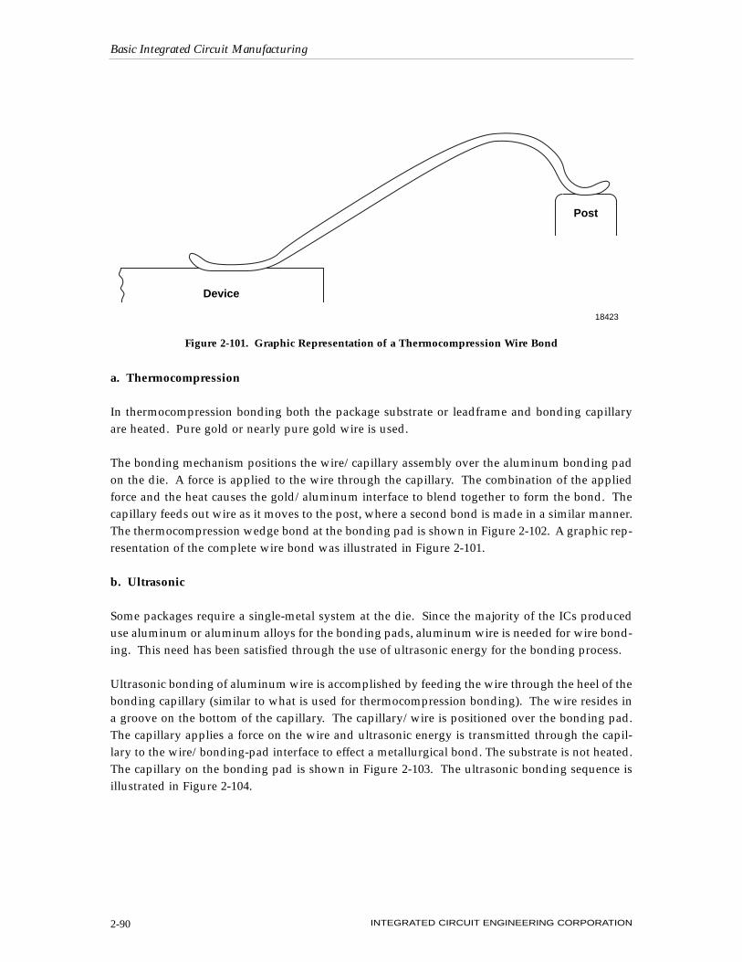
a. Thermocompression
In thermocompression bonding both the package substrate or leadframe and bonding capillaryare heated. Pure gold or nearly pure gold wire is used.
The bonding mechanism positions the wire/capillary assembly over the aluminum bonding padon the die. A force is applied to the wire through the capillary. The combination of the appliedforce and the heat causes the gold/aluminum interface to blend together to form the bond. Thecapillary feeds out wire as it moves to the post, where a second bond is made in a similar manner.The thermocompression wedge bond at the bonding pad is shown in Figure 2-102. A graphic rep-resentation of the complete wire bond was illustrated in Figure 2-101.
b. Ultrasonic
Some packages require a single-metal system at the die. Since the majority of the ICs produceduse aluminum or aluminum alloys for the bonding pads, aluminum wire is needed for wire bond-ing. This need has been satisfied through the use of ultrasonic energy for the bonding process.
Ultrasonic bonding of aluminum wire is accomplished by feeding the wire through the heel of thebonding capillary (similar to what is used for thermocompression bonding). The wire resides ina groove on the bottom of the capillary. The capillary/wire is positioned over the bonding pad.The capillary applies a force on the wire and ultrasonic energy is transmitted through the capil-lary to the wire/bonding-pad interface to effect a metallurgical bond. The substrate is not heated.The capillary on the bonding pad is shown in Figure 2-103. The ultrasonic bonding sequence isillustrated in Figure 2-104.
Basic Integrated Circuit Manufacturing
INTEGRATED CIRCUIT ENGINEERING CORPORATION2-90
Device
Post
18423
Figure 2-101. Graphic Representation of a Thermocompression Wire Bond
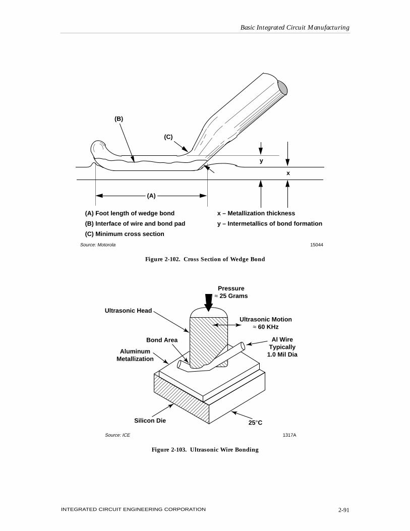
Basic Integrated Circuit Manufacturing
INTEGRATED CIRCUIT ENGINEERING CORPORATION 2-91
(A)
(B)
(C)
x
y
(A) Foot length of wedge bond
(B) Interface of wire and bond pad
(C) Minimum cross section
15044Source: Motorola
x – Metallization thickness
y – Intermetallics of bond formation
Figure 2-102. Cross Section of Wedge Bond
Pressure≈ 25 Grams
Ultrasonic Motion≈ 60 KHz
Al WireTypically
1.0 Mil Dia
25°CSilicon Die
AluminumMetallization
Bond Area
Ultrasonic Head
1317ASource: ICE
Figure 2-103. Ultrasonic Wire Bonding
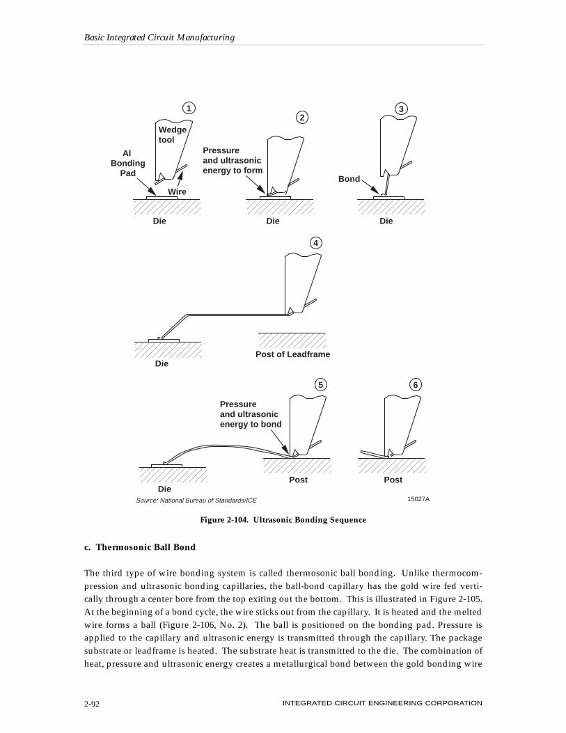
c. Thermosonic Ball Bond
The third type of wire bonding system is called thermosonic ball bonding. Unlike thermocom-pression and ultrasonic bonding capillaries, the ball-bond capillary has the gold wire fed verti-cally through a center bore from the top exiting out the bottom. This is illustrated in Figure 2-105.At the beginning of a bond cycle, the wire sticks out from the capillary. It is heated and the meltedwire forms a ball (Figure 2-106, No. 2). The ball is positioned on the bonding pad. Pressure isapplied to the capillary and ultrasonic energy is transmitted through the capillary. The packagesubstrate or leadframe is heated. The substrate heat is transmitted to the die. The combination ofheat, pressure and ultrasonic energy creates a metallurgical bond between the gold bonding wire
Basic Integrated Circuit Manufacturing
INTEGRATED CIRCUIT ENGINEERING CORPORATION2-92
Wedgetool
Die
Wire
Pressure and ultrasonicenergy to form
Bond
231
4
Post of Leadframe
5
Post
6
Post
Pressure and ultrasonicenergy to bond
15027ASource: National Bureau of Standards/ICE
Al Bonding
Pad
Die Die
Die
Die
Figure 2-104. Ultrasonic Bonding Sequence
and the aluminum metallization. The capillary is moved to the package bonding post and prop-erly positioned. The wire is now exiting from one side of the tip of the capillary. Pressure andheat cause the wire to be attached to the post. The second bond shape is partially controlled bythe physical shape of the inside bore of the capillary. The inside chamfer (radius) causes the wireto be thinned enough during the second bond such that a slight upward motion at the end of thebonding cycle breaks the wire. The inside chamfer is shown in Figure 2-107. A completed ballbond is shown in Figure 2-108.
The ball bonding system has excellent control of the wire loop. Loop control is an importantparameter in packaging. The packaging trend continues toward thinner package profiles. Thethinner the package the greater the demand on loop control. An example of loop control is illus-trated in Figure 2-109.
Basic Integrated Circuit Manufacturing
INTEGRATED CIRCUIT ENGINEERING CORPORATION 2-93
TungstenCarbide or
Glass/CeramicCapillary
Al
Die
0.0007in. to 0.002in. Au
175 – 225°CCold
N2 at 2 CFH
50 Grams
Wire:
Substrate:
Needle:
Gas:
Weight:
1827CSource: ICE
Figure 2-105. Ball Bonding
Basic Integrated Circuit Manufacturing
INTEGRATED CIRCUIT ENGINEERING CORPORATION2-94
Die
Die
Die
Die
Capillarytool
Goldwire
1 2
3
Pressure,ultrasonic energy and heat to form
Ballbond
Post of Leadframe
5
4
Electronic flame-off
stitchbond
PostPost
Pressureand heatto form
6
7 8
15022ASource: National Bureau of Standards/ICE
BallAl
BondingPad
Figure 2-106. Thermocompression/Thermosonic Bonding Sequence
Basic Integrated Circuit Manufacturing
INTEGRATED CIRCUIT ENGINEERING CORPORATION 2-95
Standard 90° chamfer provides a less sharp transition than the 120° style. This transition
causes less drag on the wire allowingimproved looping
The 90° double chamfer is standardon all Gaiser 90° tools.
The 120° double chamfer provides a less sharptransition allowing improved looping while
producing a strong tail bond.
The radiused 120° chamfer provides the bestlooping while providing a strong tail bond.
90°50°90°
120°90°
120°
Radius EdgeReduces Wire Drag
Source: Gaiser Tool Company 15067
Figure 2-107. Inside Chamfer Discussion
Bonding padon die
(B)
(A)
(A) Final ball bond diameter
(B) Interface of wire and bond pad
(C) Neck area of wire15021A
Lead frame or post bond
(C)
Figure 2-108. Cross Section of Ball Bond
The wire bonding process is con-trolled by having a good StatisticalProcess Control program. Part ofthis program will be a sample visualinspection, wire pull testing, andball shear testing. The pull test datashould be categorized for any bondfailure. Generally the five cate-gories shown in Figure 2-110 areused. Each of these categories mustbe monitored closely, particularly
the lifted bond. The ball shear test should serve to guard against lifted bond failures that wouldnot be detected by the conventional wire pull test.
Wire bonding technologies summarized in Figure 2-111. This figure also shows the better pro-ductivity of the thermosonic bonding system.
One of the future challenges facing the wire bond method of lead attach is the need to bond tosmaller bonding pads placed closer together. Part of the spacing issue centers on the use of stag-gered bonding pads, often referred to as "zero pitch" (Figure 2-112).
Basic Integrated Circuit Manufacturing
INTEGRATED CIRCUIT ENGINEERING CORPORATION2-96
18424
Figure 2-109. Loop Control of Wire Bonds
• Lift at bonding pad metal
• Lift at leadframe
• Break at heel of bond (leadframe)
• Break at ball (neck - down)
• Center wire break
Figure 2-110. Wire Bond Failure Categories
15020
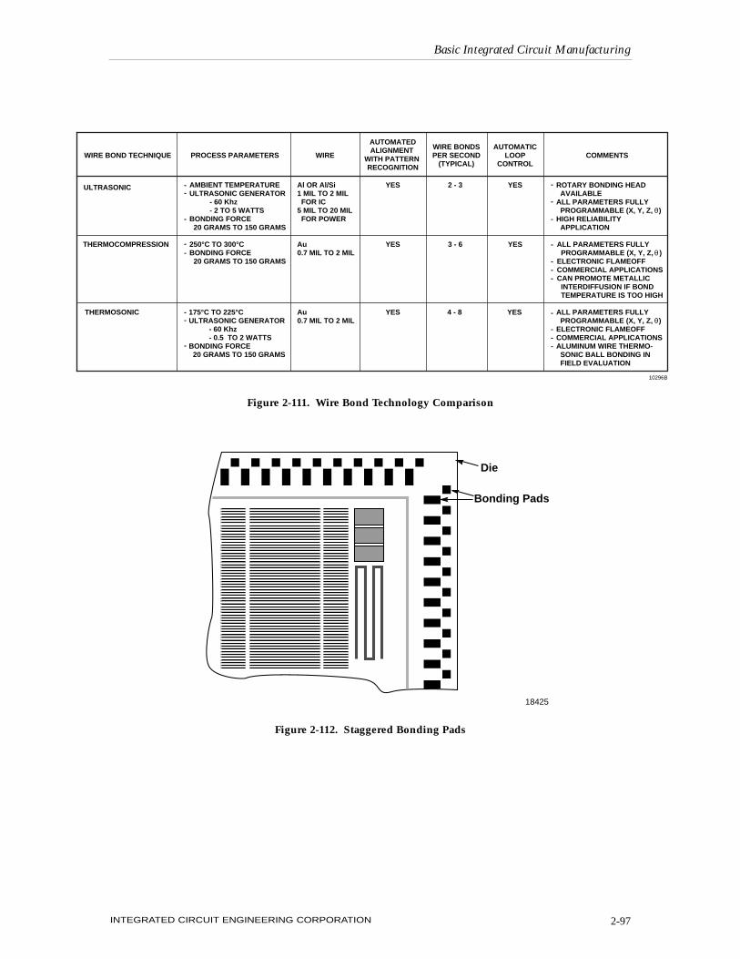
Basic Integrated Circuit Manufacturing
INTEGRATED CIRCUIT ENGINEERING CORPORATION 2-97
Al OR Al/Si1 MIL TO 2 MIL FOR IC5 MIL TO 20 MIL FOR POWER
Au0.7 MIL TO 2 MIL
Au0.7 MIL TO 2 MIL
WIRE
YES
YES
YES
AUTOMATEDALIGNMENT
WITH PATTERN RECOGNITION
YES
YES
YES
AUTOMATICLOOP
CONTROL
ULTRASONIC
THERMOCOMPRESSION
THERMOSONIC
WIRE BOND TECHNIQUE
3 - 6
4 - 8
WIRE BONDSPER SECOND
(TYPICAL)
2 - 3
PROCESS PARAMETERS
250°C TO 300°CBONDING FORCE 20 GRAMS TO 150 GRAMS
--
AMBIENT TEMPERATUREULTRASONIC GENERATOR - 60 Khz - 2 TO 5 WATTSBONDING FORCE 20 GRAMS TO 150 GRAMS
-
--
175°C TO 225°CULTRASONIC GENERATOR - 60 Khz - 0.5 TO 2 WATTSBONDING FORCE 20 GRAMS TO 150 GRAMS
--
-
COMMENTS
ALL PARAMETERS FULLY PROGRAMMABLE (X, Y, Z, )ELECTRONIC FLAMEOFFCOMMERCIAL APPLICATIONSCAN PROMOTE METALLIC INTERDIFFUSION IF BOND TEMPERATURE IS TOO HIGH
ROTARY BONDING HEAD AVAILABLEALL PARAMETERS FULLY PROGRAMMABLE (X, Y, Z, )
APPLICATION
ALL PARAMETERS FULLY PROGRAMMABLE (X, Y, Z, )ELECTRONIC FLAMEOFFCOMMERCIAL APPLICATIONSALUMINUM WIRE THERMO- SONIC BALL BONDING IN FIELD EVALUATION
HIGH RELIABILITY
-
---
-
---
-
-
-
θ
θ
θ
10296B
Figure 2-111. Wire Bond Technology Comparison
Bonding Pads
18425
Die
Figure 2-112. Staggered Bonding Pads
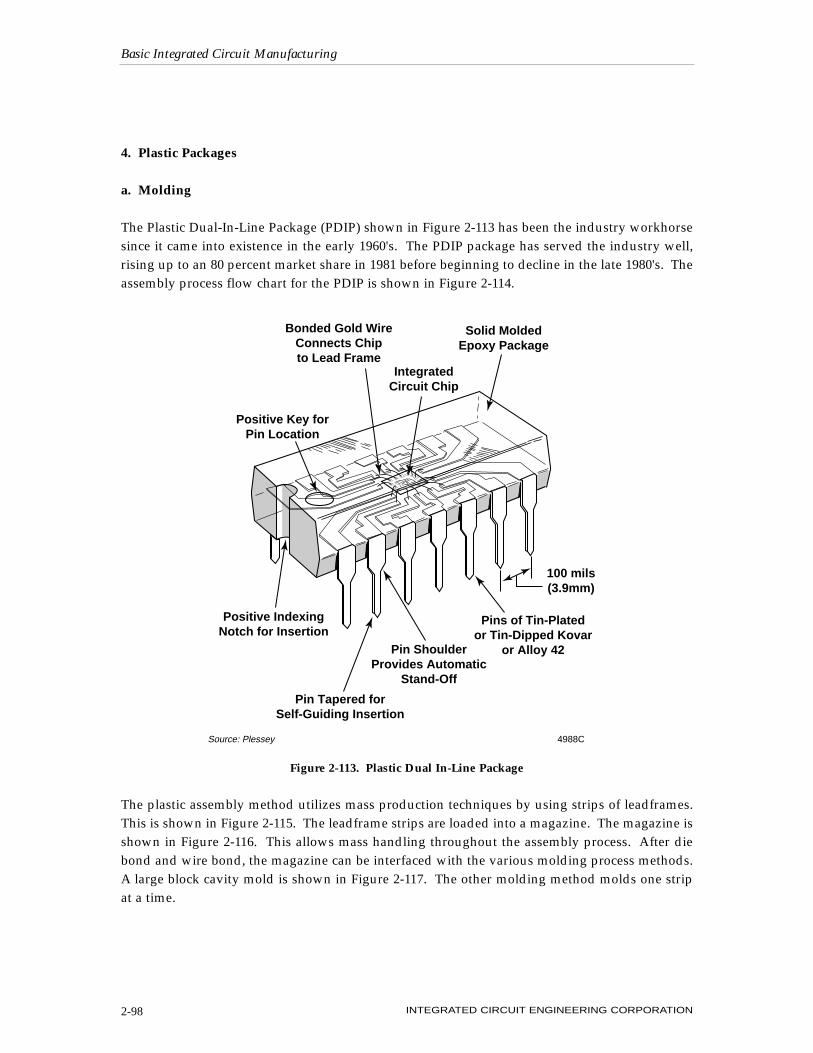
4. Plastic Packages
a. Molding
The Plastic Dual-In-Line Package (PDIP) shown in Figure 2-113 has been the industry workhorsesince it came into existence in the early 1960's. The PDIP package has served the industry well,rising up to an 80 percent market share in 1981 before beginning to decline in the late 1980's. Theassembly process flow chart for the PDIP is shown in Figure 2-114.
The plastic assembly method utilizes mass production techniques by using strips of leadframes.This is shown in Figure 2-115. The leadframe strips are loaded into a magazine. The magazine isshown in Figure 2-116. This allows mass handling throughout the assembly process. After diebond and wire bond, the magazine can be interfaced with the various molding process methods.A large block cavity mold is shown in Figure 2-117. The other molding method molds one stripat a time.
Basic Integrated Circuit Manufacturing
INTEGRATED CIRCUIT ENGINEERING CORPORATION2-98
Bonded Gold WireConnects Chipto Lead Frame
Solid MoldedEpoxy Package
IntegratedCircuit Chip
Positive Key forPin Location
Positive IndexingNotch for Insertion
Pin Tapered for Self-Guiding Insertion
Pins of Tin-Platedor Tin-Dipped Kovar
or Alloy 42Pin ShoulderProvides Automatic
Stand-Off
4988CSource: Plessey
100 mils(3.9mm)
Figure 2-113. Plastic Dual In-Line Package
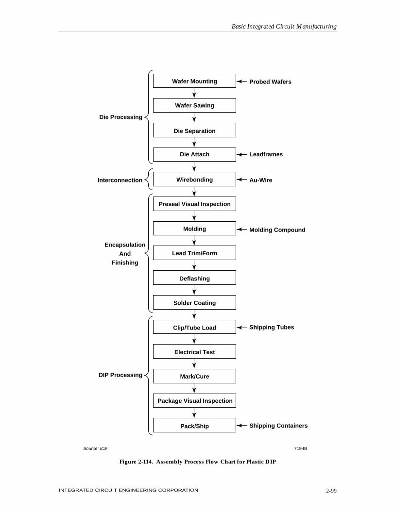
Basic Integrated Circuit Manufacturing
INTEGRATED CIRCUIT ENGINEERING CORPORATION 2-99
Wafer Mounting
Wafer Sawing
Die Separation
Die Attach
Wirebonding
Preseal Visual Inspection
Molding
Lead Trim/Form
Deflashing
Solder Coating
Clip/Tube Load
Electrical Test
Mark/Cure
Package Visual Inspection
Pack/Ship
Probed Wafers
Leadframes
Au-Wire
Molding Compound
Shipping Tubes
Shipping Containers
Die Processing
Interconnection
Encapsulation
And
Finishing
DIP Processing
7194BSource: ICE
Figure 2-114. Assembly Process Flow Chart for Plastic DIP
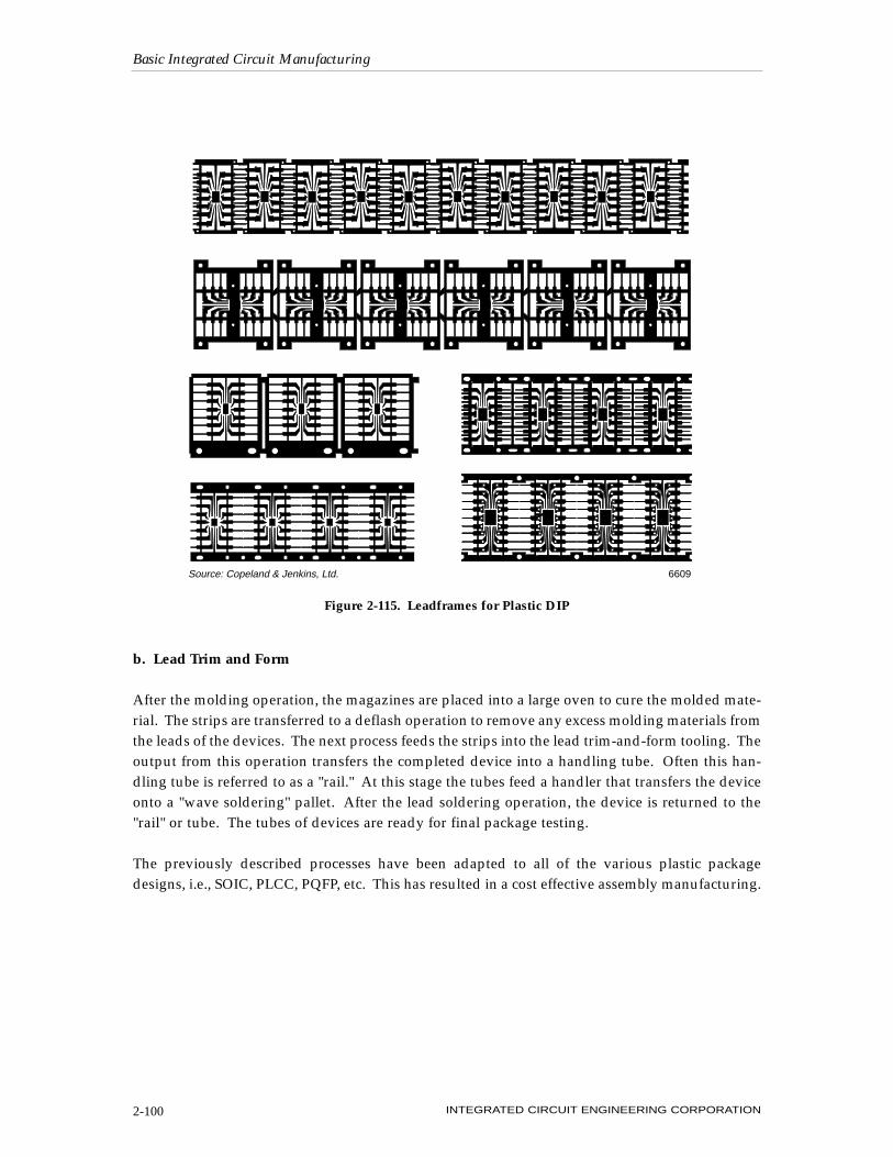
b. Lead Trim and Form
After the molding operation, the magazines are placed into a large oven to cure the molded mate-rial. The strips are transferred to a deflash operation to remove any excess molding materials fromthe leads of the devices. The next process feeds the strips into the lead trim-and-form tooling. Theoutput from this operation transfers the completed device into a handling tube. Often this han-dling tube is referred to as a "rail." At this stage the tubes feed a handler that transfers the deviceonto a "wave soldering" pallet. After the lead soldering operation, the device is returned to the"rail" or tube. The tubes of devices are ready for final package testing.
The previously described processes have been adapted to all of the various plastic packagedesigns, i.e., SOIC, PLCC, PQFP, etc. This has resulted in a cost effective assembly manufacturing.
Basic Integrated Circuit Manufacturing
INTEGRATED CIRCUIT ENGINEERING CORPORATION2-100
6609Source: Copeland & Jenkins, Ltd.
Figure 2-115. Leadframes for Plastic DIP
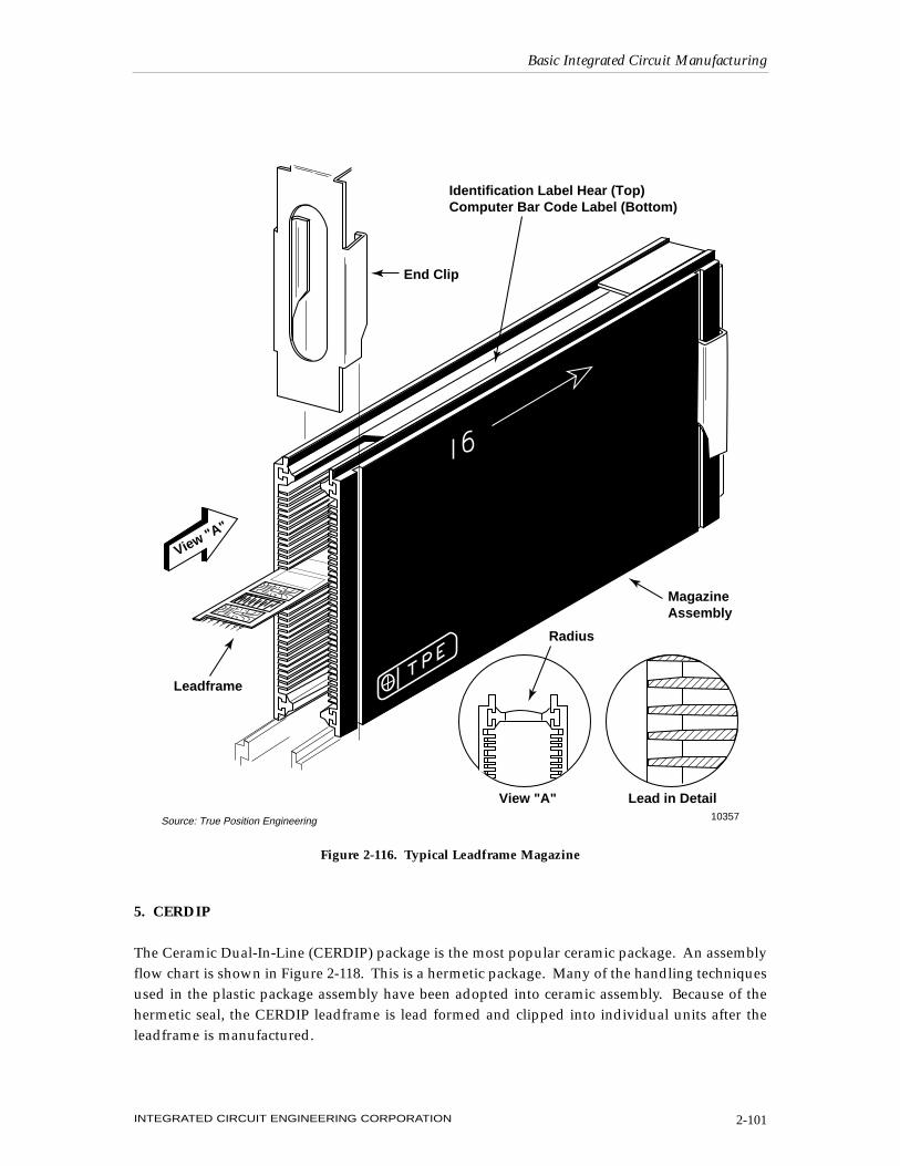
5. CERDIP
The Ceramic Dual-In-Line (CERDIP) package is the most popular ceramic package. An assemblyflow chart is shown in Figure 2-118. This is a hermetic package. Many of the handling techniquesused in the plastic package assembly have been adopted into ceramic assembly. Because of thehermetic seal, the CERDIP leadframe is lead formed and clipped into individual units after theleadframe is manufactured.
Basic Integrated Circuit Manufacturing
INTEGRATED CIRCUIT ENGINEERING CORPORATION 2-101
Leadframe
Radius
View "A"
MagazineAssembly
Lead in Detail
End Clip
View "A"
Identification Label Hear (Top)Computer Bar Code Label (Bottom)
Source: True Position Engineering 10357
Figure 2-116. Typical Leadframe Magazine
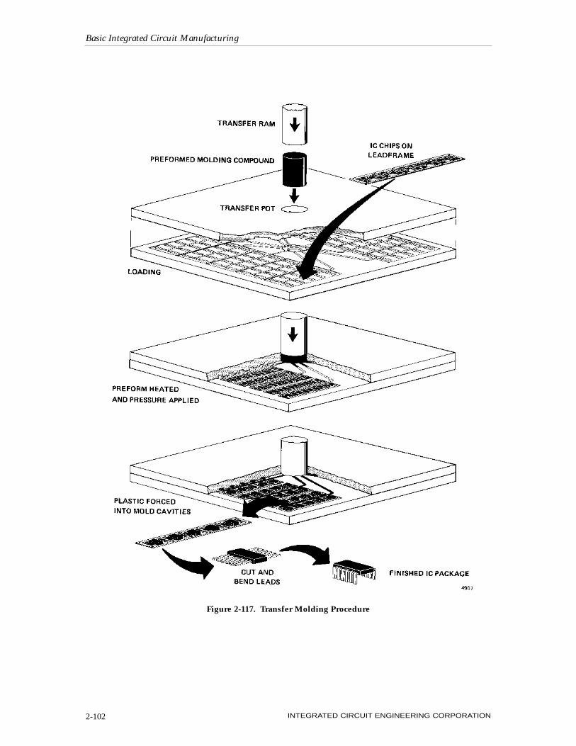
Basic Integrated Circuit Manufacturing
INTEGRATED CIRCUIT ENGINEERING CORPORATION2-102
Figure 2-117. Transfer Molding Procedure
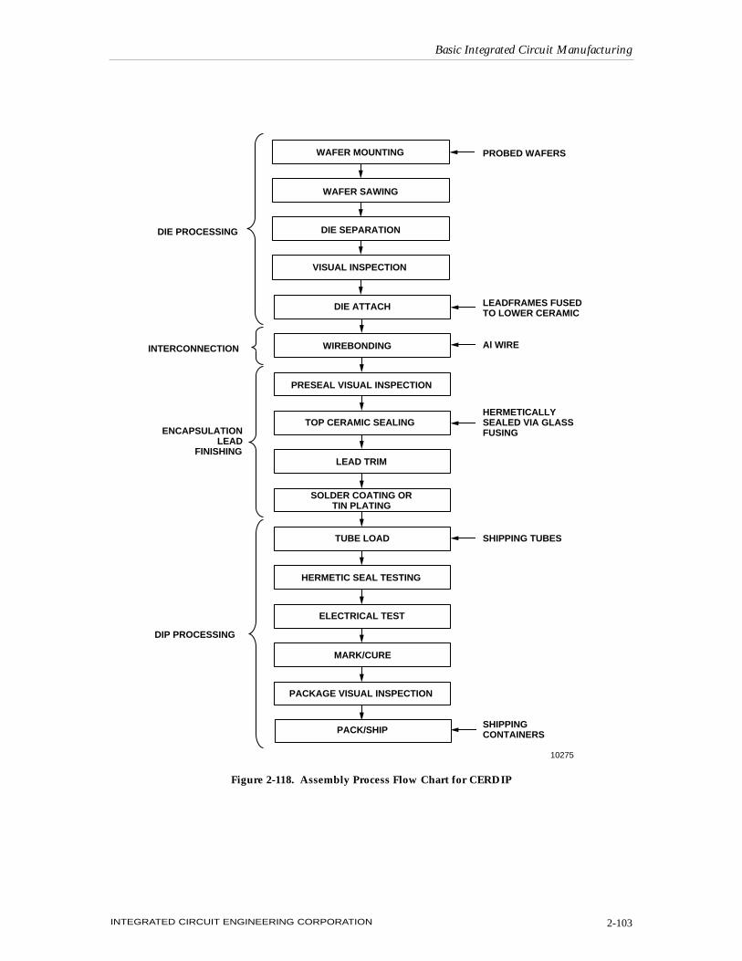
Basic Integrated Circuit Manufacturing
INTEGRATED CIRCUIT ENGINEERING CORPORATION 2-103
DIE PROCESSING
INTERCONNECTION
ENCAPSULATIONLEAD
FINISHING
DIP PROCESSING
PROBED WAFERS
LEADFRAMES FUSEDTO LOWER CERAMIC
HERMETICALLYSEALED VIA GLASSFUSING
SHIPPING TUBES
SHIPPINGCONTAINERS
WAFER MOUNTING
WAFER SAWING
DIE SEPARATION
DIE ATTACH
WIREBONDING
PRESEAL VISUAL INSPECTION
TOP CERAMIC SEALING
LEAD TRIM
SOLDER COATING ORTIN PLATING
TUBE LOAD
HERMETIC SEAL TESTING
ELECTRICAL TEST
MARK/CURE
PACKAGE VISUAL INSPECTION
Al WIRE
PACK/SHIP
VISUAL INSPECTION
10275
Figure 2-118. Assembly Process Flow Chart for CERDIP
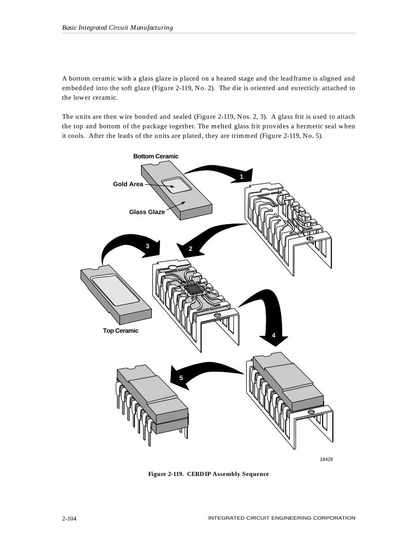
A bottom ceramic with a glass glaze is placed on a heated stage and the leadframe is aligned andembedded into the soft glaze (Figure 2-119, No. 2). The die is oriented and eutecticly attached tothe lower ceramic.
The units are then wire bonded and sealed (Figure 2-119, Nos. 2, 3). A glass frit is used to attachthe top and bottom of the package together. The melted glass frit provides a hermetic seal whenit cools. After the leads of the units are plated, they are trimmed (Figure 2-119, No. 5).
Basic Integrated Circuit Manufacturing
INTEGRATED CIRCUIT ENGINEERING CORPORATION2-104
18426
5
1
23
4
Gold Area
Glass Glaze
Top Ceramic
Bottom Ceramic
Figure 2-119. CERDIP Assembly Sequence
The final testing of the packaged device is done by automated handlers interfaced with the appro-priate tester. In many test areas, the marking equipment is configured in-line with the testing tocomplete the manufacturing cycle. An in-line Q.C./Q.A. function is integrated into the test area.
There are many other package types used for ICs. The assembly processes for these packages aremodifications of the plastic and ceramic assembly methods already presented.
K. PROBE AND TEST
1. Wafer Testing
a. Test Patterns
The electrical evaluation of an IC in wafer form requires two different types of testing. The firstelectrical test is performed on "test pattern" structures. The other electrical evaluation is the test-ing of the IC to a given electrical specification.
The "test pattern" structures are arrangements of individual test patterns, each designed to evalu-ate specific process attributes. For example, there will be enhancement mode and depletion modetransistors of various geometrical sizes to represent the circuit elements, resistivity structures, crit-ical dimension and overlay registration structures, defect density structures, interconnect teststructures for metal step coverage, contact resistance, electromigration, stress migration, and par-asitic circuit structures.
All of these test structures' electrical characteristics are measured, recorded, and correlated to thevarious real-time test wafer measurements taken after each critical process step is completed.
The maturity of the product, the specific technology, the type of photo equipment, and the engi-neering management will determine where the test structures are arranged on the wafer and thestatistics used to accept individual wafers or the wafer lot. Generally the "test patterns" are sam-pled statistically on the wafer and wafers in a lot.
If a sample fails the electrical criteria, the lot will be judged by engineering for further action.Some of the possibilities are:
1. Test additional samples2. Test all wafers3. Reject wafers failing the criteria4. Reject the lot
Basic Integrated Circuit Manufacturing
INTEGRATED CIRCUIT ENGINEERING CORPORATION 2-105
b. Probe Testing
The wafers receive a 100 percent wafer probe evaluation after the "test patterns" are evaluated.This testing is product specific to data sheet or customer requirements. This test of the wafer hasbeen primarily a room temperature test. However, there is a trend to raise the substrate temper-ature to 50°C. Higher temperatures will cause temperature-sensitive parameters to change, allow-ing a more critical evaluation.
Each whole die on the wafer is tested. The probe machine moves the wafer to a location under aset of probe needles. The probe needles are lined up with the bonding pads of the first die to betested. The needles are lowered onto the die (or the die is raised to come into contact with the nee-dles) and that die is tested. The needles separate from the die and the wafer moves to a positionwhere the needles are lined up with another die. The cycle is repeated until all of the whole diceon the wafer are tested. The dice that fail the test are identified, usually with a drop of ink.
After the 100 percent wafer testing is completed, the wafers are sent to the assembly process forfinal packaging.
2. Final (Product) Testing
The final testing of the product after packaging tests the product to the data sheet specification orto a customer-specific test requirement. A variety of final tests are performed to check for speci-fied electrical characteristics.
Automation is used in a majority of the final test activities. Only when a package is new to theindustry or customized and does not fit existing hardware will hand insertion to a socket be used.Bent leads or poor lead finish on a package can cause severe problems for final test. Thus, automa-tion is necessary to prevent these and other problems.
3. Burn-in
"Burn-in" typically follows Final Test. The use of "burn-in" evolved from semiconductors used inmilitary systems in the early 1960's. The concept has stayed with semiconductor manufacturingin varying degrees. The reason for applying voltage to a semiconductor device at an elevated tem-perature for some period of time is illustrated in Figure 2-120. This is considered a "stress test."From a reliability point of view the elevated temperature with voltage applied for a given timeperiod will cause marginal devices to fail. This removes a potential "field failure." The screeningis intended to improve the statistical level of reliability by removing the "infant motality" devices.
This "burn-in" screen is used in many different ways by the semiconductor industry. Within agiven company the "burn-in" conditions vary over products and technologies.
Basic Integrated Circuit Manufacturing
INTEGRATED CIRCUIT ENGINEERING CORPORATION2-106
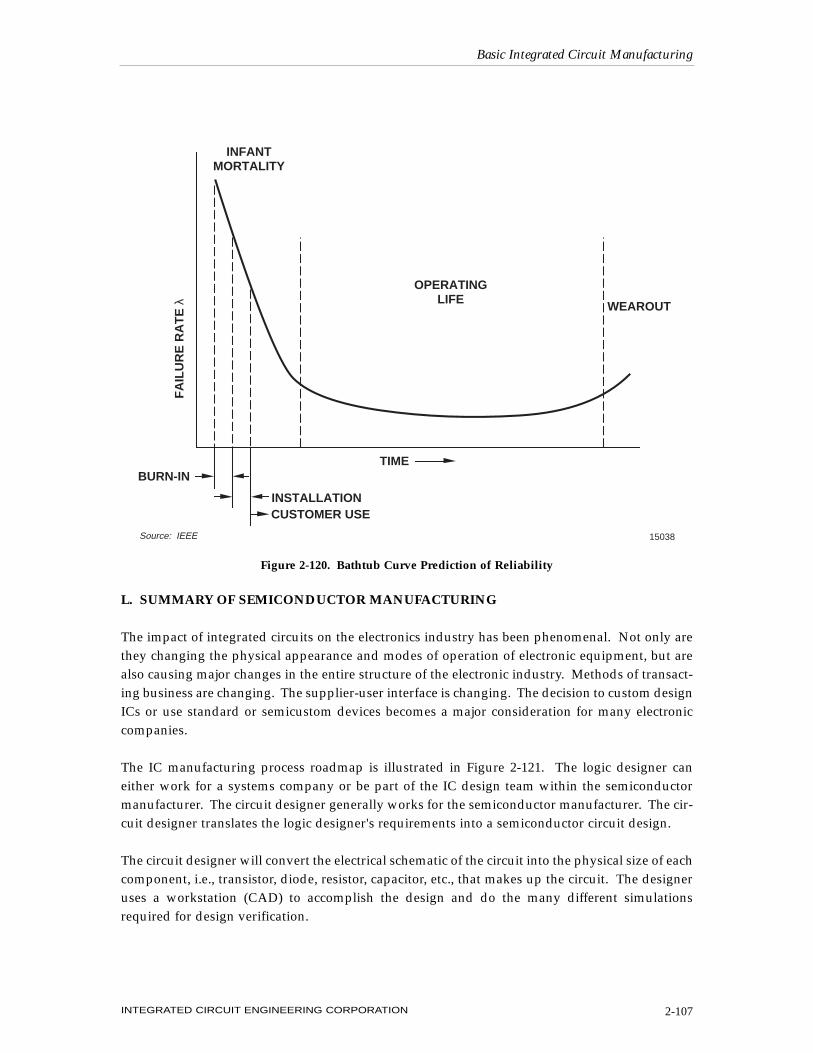
L. SUMMARY OF SEMICONDUCTOR MANUFACTURING
The impact of integrated circuits on the electronics industry has been phenomenal. Not only arethey changing the physical appearance and modes of operation of electronic equipment, but arealso causing major changes in the entire structure of the electronic industry. Methods of transact-ing business are changing. The supplier-user interface is changing. The decision to custom designICs or use standard or semicustom devices becomes a major consideration for many electroniccompanies.
The IC manufacturing process roadmap is illustrated in Figure 2-121. The logic designer caneither work for a systems company or be part of the IC design team within the semiconductormanufacturer. The circuit designer generally works for the semiconductor manufacturer. The cir-cuit designer translates the logic designer's requirements into a semiconductor circuit design.
The circuit designer will convert the electrical schematic of the circuit into the physical size of eachcomponent, i.e., transistor, diode, resistor, capacitor, etc., that makes up the circuit. The designeruses a workstation (CAD) to accomplish the design and do the many different simulationsrequired for design verification.
Basic Integrated Circuit Manufacturing
INTEGRATED CIRCUIT ENGINEERING CORPORATION 2-107
INFANTMORTALITY
BURN-IN
INSTALLATIONCUSTOMER USE
OPERATINGLIFE WEAROUT
TIME
FA
ILU
RE
RA
TE
λ
15038Source: IEEE
Figure 2-120. Bathtub Curve Prediction of Reliability
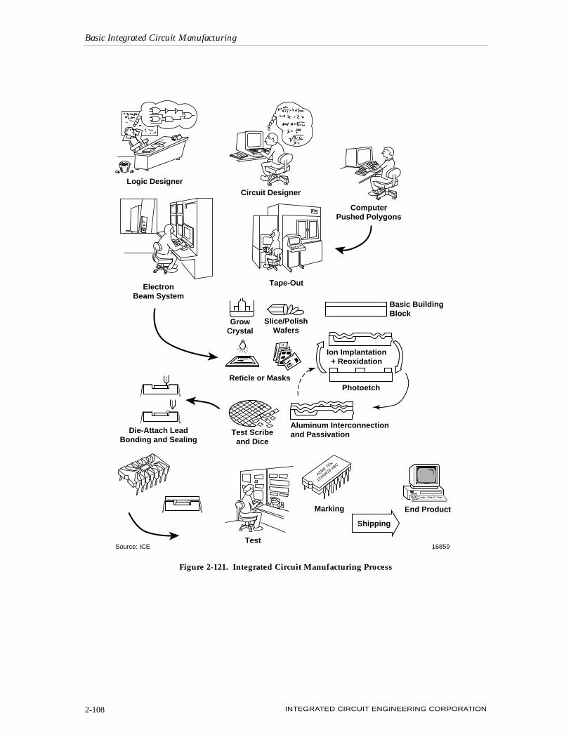
Basic Integrated Circuit Manufacturing
INTEGRATED CIRCUIT ENGINEERING CORPORATION2-108
Logic DesignerCircuit Designer
ComputerPushed Polygons
Tape-Out
Reticle or Masks
ElectronBeam System
Ion Implantation+ Reoxidation
Photoetch
GrowCrystal
Slice/PolishWafers
Basic BuildingBlock
Aluminum Interconnectionand PassivationTest Scribe
and DiceDie-Attach Lead
Bonding and Sealing
Marking
Shipping
End Product
Test16859Source: ICE
ACME TEK
12345678 ABC
Figure 2-121. Integrated Circuit Manufacturing Process
The geometrical layout is the final output of the workstation in the form of a database tape. Thedatabase tape is the input information for the electron-beam system. The electron-beam systemuses the input data to create the reticles or masks required in IC manufacturing. The number ofreticles or masks is determined by the actual manufacturing process cycle. This is often referredto as the "Fab Process." The newer Fab Processes use between fourteen and twenty-four reticlesor masks.
The central region of Figure 2-121 depicts the wafer fab process. After the wafer fab process iscompleted, the wafers are tested electrically to the required specifications and then forwarded tothe assembly process.
The assembly process will package each electrically good die. After packaging is completed, thedevice will be given a final electrical test, burn-in as required, and shipped to the end user. Theend user creates the electronic system by bringing together all the necessary electrical compo-nents, mechanical hardware and the final package of the product.
There is no doubt the world is in the silicon age. Silicon devices in the form of discrete productsor ICs touch our lives in many ways everyday. And — since silicon is the second most abundantelement in the earth, there doesn't appear there will ever be a shortage of the raw material.
Basic Integrated Circuit Manufacturing
INTEGRATED CIRCUIT ENGINEERING CORPORATION 2-109

Basic Integrated Circuit Manufacturing
INTEGRATED CIRCUIT ENGINEERING CORPORATION2-110