Embed Size (px)
Citation preview

EE 330
Lecture 8
IC Fabrication Technology
Part 1
Quiz 7 The layout of the cascade of two CMOS inverters is shown. It has
some layout errors. Identify them.

And the number is ….
6
31
2
4
5
7
8
9

And the number is ….
6
31
2
4
5
7
8
9
4

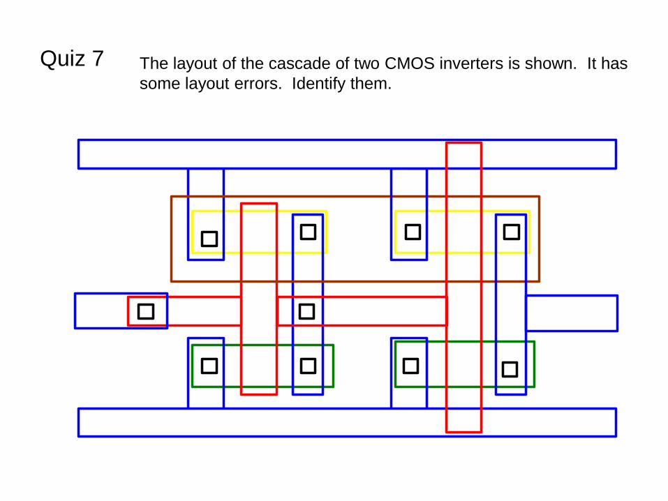
Quiz 7 Solution:
- Bulk Connection on P-well is missing
- Poly from first gate is shorted to poly from second gate (circuit error,
not DRC
Quiz 7 solution:
- Corrected Circuit
Technology Files
• Provide Information About Process – Process Flow (Fabrication Technology)
– Model Parameters
– Design Rules
• Serve as Interface Between Design Engineer and Process Engineer
• Insist on getting information that is deemed important for a design – Limited information available in academia
– Foundries often sensitive to who gets access to information
– Customer success and satisfaction is critical to foundries
Review from Last Time
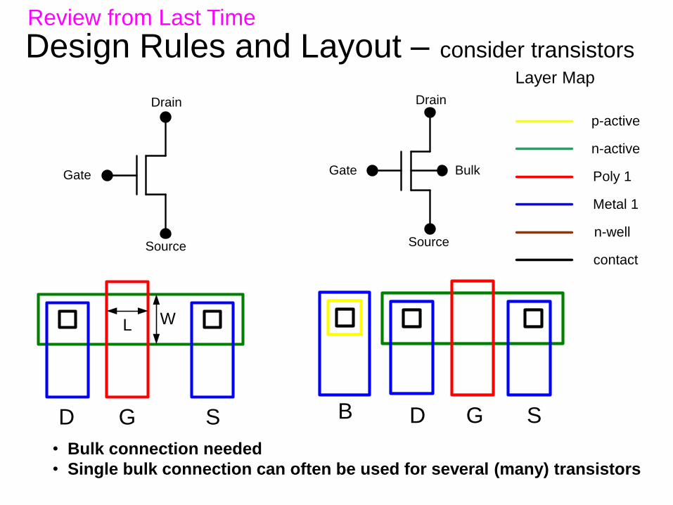
Design Rules and Layout – consider transistors
Drain
Gate
Source
Drain
Gate
Source
Bulk
p-active
n-active
Poly 1
Metal 1
n-well
contact
D SG
L W
Layer Map
D SGB
• Bulk connection needed
• Single bulk connection can often be used for several (many) transistors
Review from Last Time

Design Rules and Layout – consider transistors
D SGBD SG
Drain
Gate
Source
p-active
n-active
Poly 1
Metal 1
n-well
contact
Layer Map
• Bulk connection needed
• Single bulk connection can often be used for several (many)
transistors is they share the same well
Drain
Gate
Source
Bulk
Review from Last Time

Design Rules
• Design rules can be given in absolute dimensions for every rule
• Design rules can be parameterized and given relative to a parameter – Makes movement from one process to another more
convenient
– Easier for designer to remember
– Some penalty in area efficiency
– Often termed λ-based design rules
– Typically λ is ½ the minimum feature size in a process
Review from Last Time

Review from Last Time
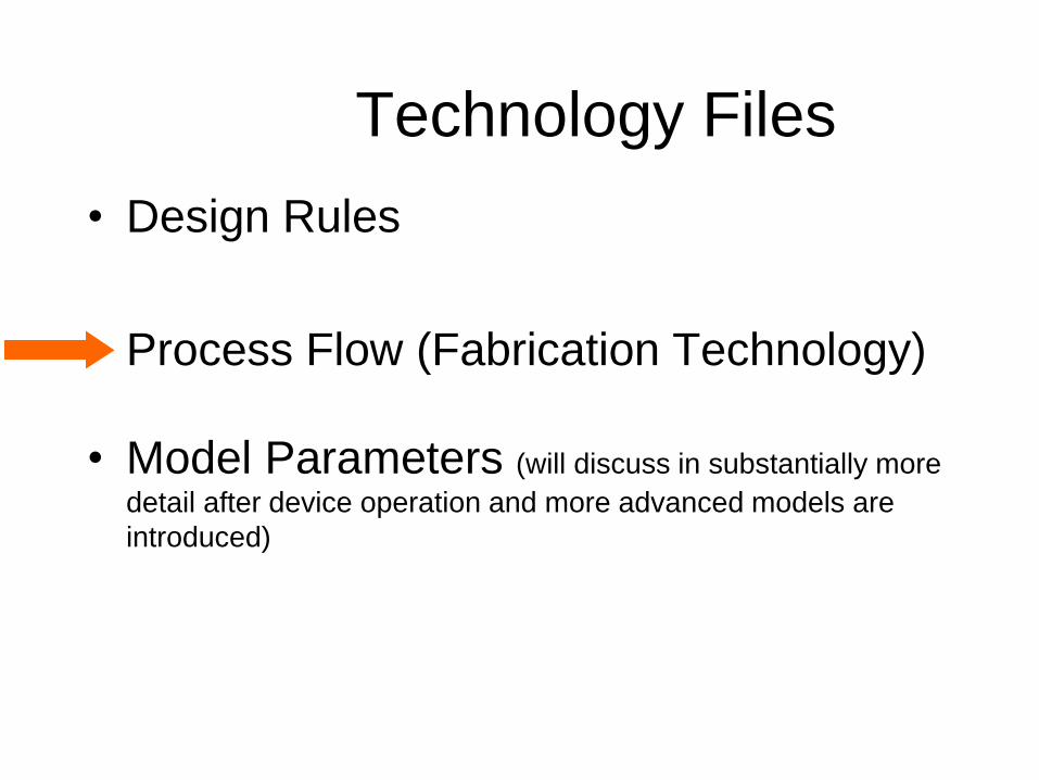
Technology Files
• Design Rules
• Process Flow (Fabrication Technology)
• Model Parameters (will discuss in substantially more
detail after device operation and more advanced models are
introduced)

IC Fabrication Technology
See Chapter 3 and a little of
Chapter 1 of WH
or Chapter 2 GAS for details

Mask Fabrication
Epitaxy
Photoresist
Etch
Strip
Planarization
Deposit or Implant
Grow or Apply
Wafer Probe
Die Attach
Wafer Dicing
Wire Attach (bonding)
Package
Test
Wafer Fabrication
Ship
Fro
nt
En
d
Back E
nd
Generic
Process
Flow

IC Fabrication Technology
• Crystal Preparation
• Masking
• Photolithographic Process
• Deposition
• Etching
• Diffusion
• Oxidation
• Epitaxy
• Polysilicon
• Contacts, Interconnect and Metalization
• Planarization
MOS Transistor
n-type
n+-type
p-type
p+-type
SiO2 (insulator)
POLY (conductor)
Drain
Gate
Source
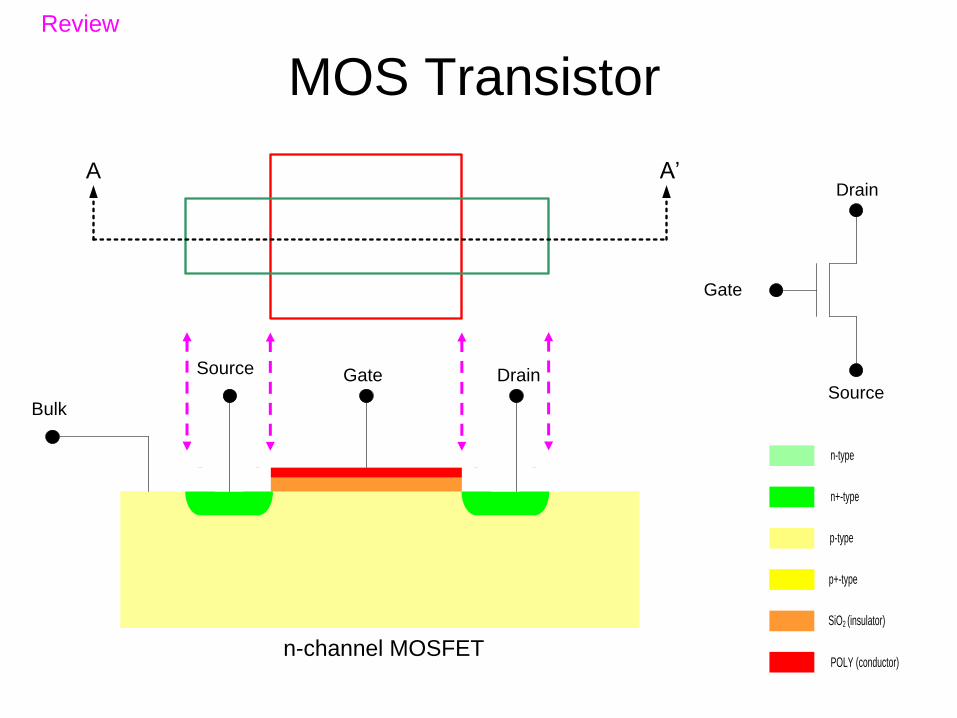
Review
A’A
Gate DrainSource
Bulk
n-channel MOSFET

MOS Transistor
Drain
Gate
Source
n-type
n+-type
p-type
p+-type
SiO2 (insulator)
POLY (conductor)
Review
Gate DrainSource
Bulk
p-channel MOSFET
A’A

MOS Transistor Gate DrainSource
Bulk
n-channel MOSFET
Gate DrainSource
Bulk
n-channel MOSFET
n-channel MOS transistor in
Bulk CMOS n-well process
with bulk contact

MOS Transistor
Gate DrainSource
Bulk
p-channel MOSFET
Gate DrainSource
Bulk
p-channel MOSFET
p-channel MOS transistor in
Bulk CMOS n-well process
with bulk contact and well (tub)
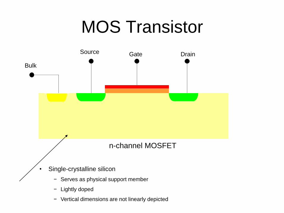
MOS Transistor
Gate DrainSource
Bulk
n-channel MOSFET
• Single-crystalline silicon
− Serves as physical support member
− Lightly doped
− Vertical dimensions are not linearly depicted

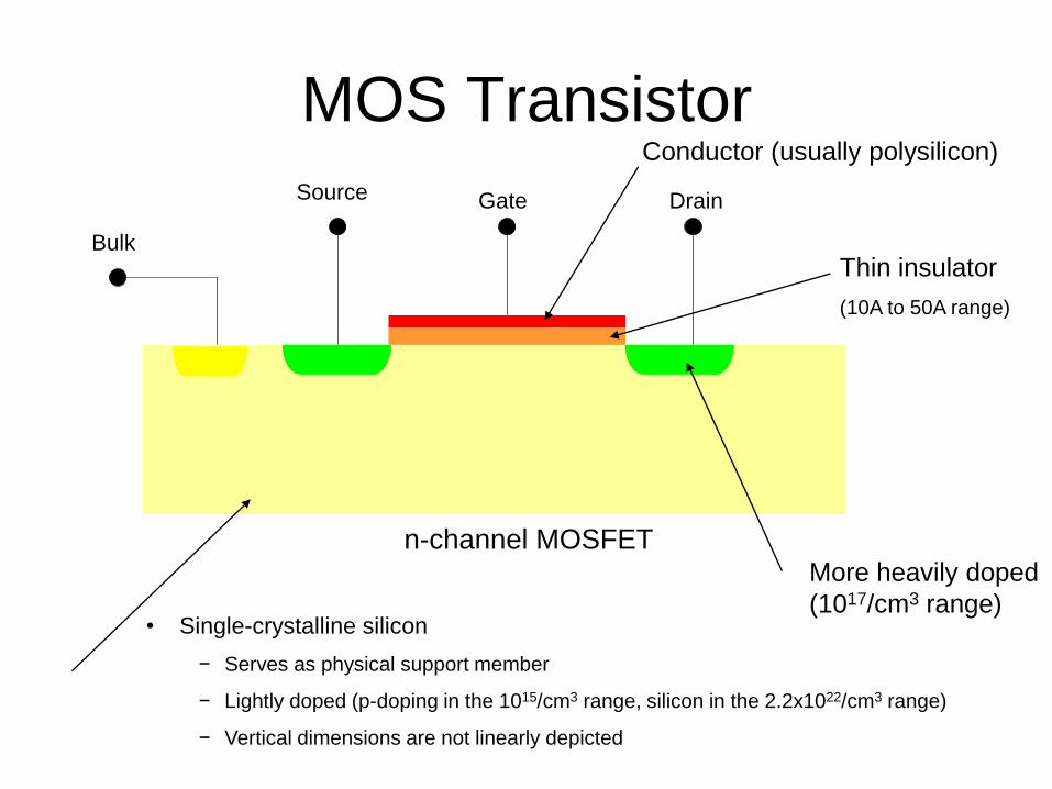
MOS Transistor
Gate DrainSource
Bulk
n-channel MOSFET
• Single-crystalline silicon
− Serves as physical support member
− Lightly doped
− Vertical dimensions are not linearly depicted
MOS Transistor
Gate DrainSource
Bulk
n-channel MOSFET
• Single-crystalline silicon
− Serves as physical support member
− Lightly doped (p-doping in the 1015/cm3 range, silicon in the 2.2x10²²/cm3 range)
− Vertical dimensions are not linearly depicted
Thin insulator
(10A to 50A range)
Conductor (usually polysilicon)
More heavily doped
(1017/cm3 range)

MOS Transistor
Gate DrainSource
Bulk
p-channel MOSFET
Lightly-doped n-type
(5x10¹⁶/cm3 range)
More heavily-doped p-type
(1018/cm3 range)
Lightly doped p-type
(1015/cm3 range)
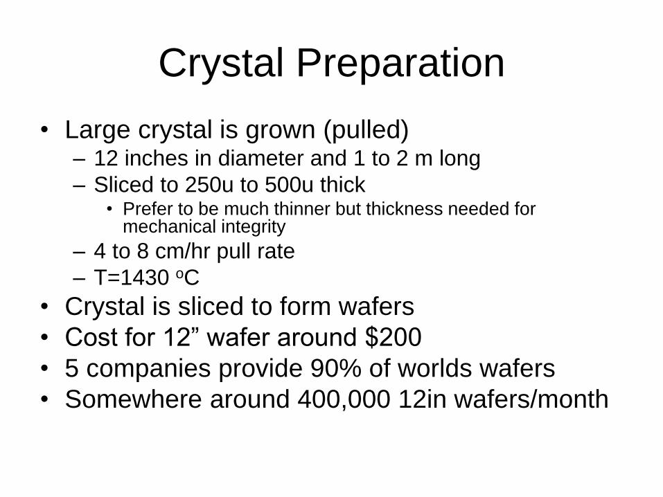
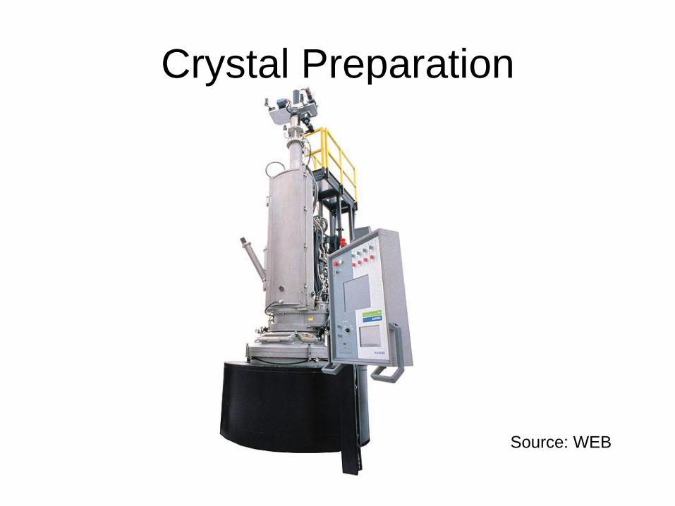
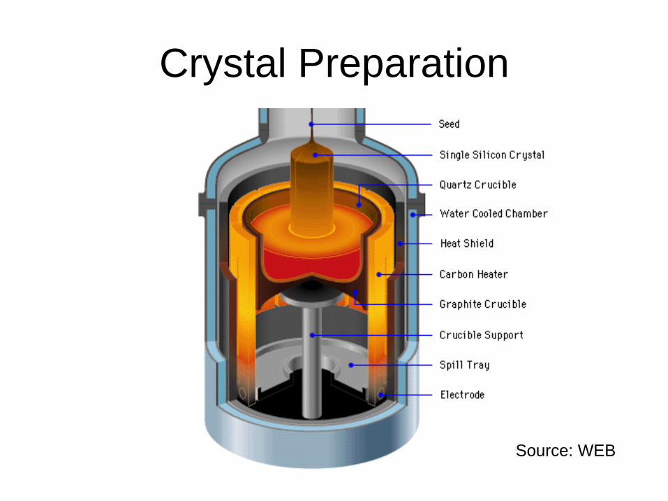
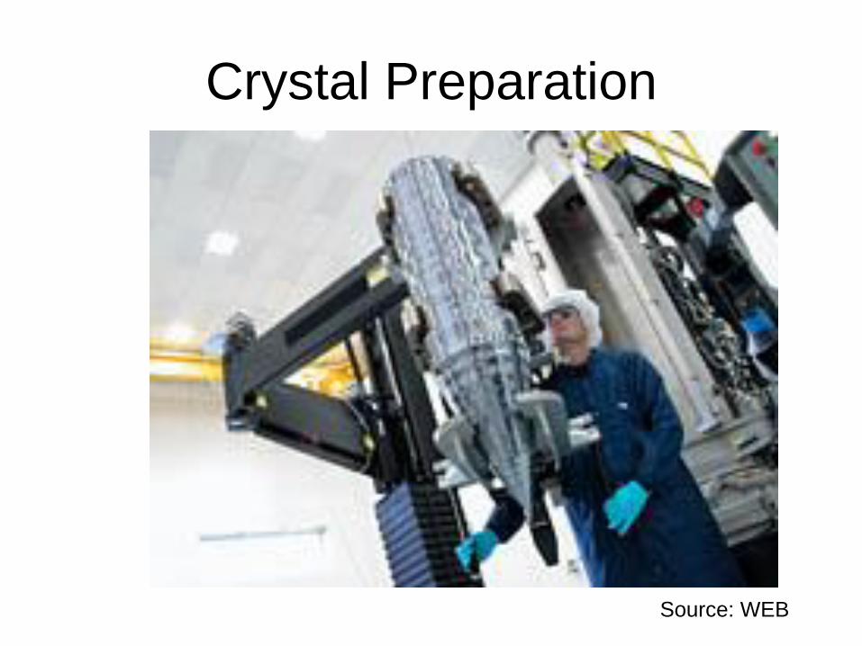
Crystal Preparation
• Large crystal is grown (pulled) – 12 inches in diameter and 1 to 2 m long
– Sliced to 250u to 500u thick • Prefer to be much thinner but thickness needed for
mechanical integrity
– 4 to 8 cm/hr pull rate
– T=1430 oC
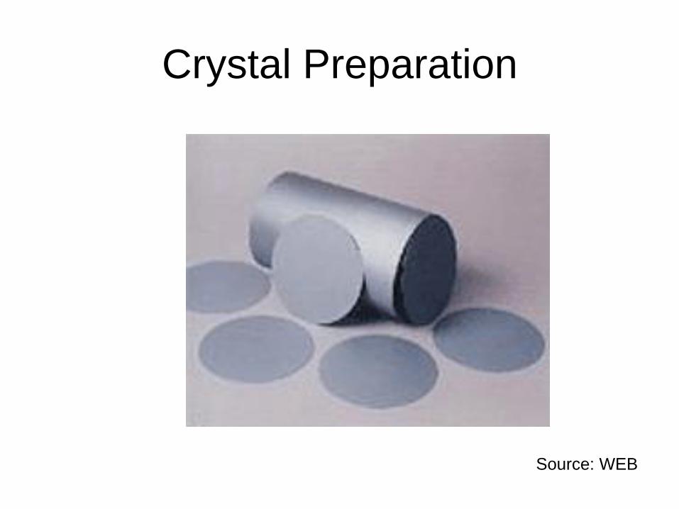
• Crystal is sliced to form wafers
• Cost for 12” wafer around $200
• 5 companies provide 90% of worlds wafers
• Somewhere around 400,000 12in wafers/month
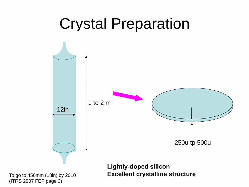
Crystal Preparation
12in 1 to 2 m
250u tp 500u
Lightly-doped silicon
Excellent crystalline structure To go to 450mm (18in) by 2010
(ITRS 2007 FEP page 3)

Crystal Preparation
From www.infras.com
Crystal Preparation
Source: WEB
Crystal Preparation
Source: WEB
Crystal Preparation
Source: WEB

Crystal Preparation
Source: WEB
Crystal Preparation
Source: WEB

IC Fabrication Technology
• Crystal Preparation
• Masking
• Photolithographic Process
• Deposition
• Etching
• Diffusion
• Oxidation
• Epitaxy
• Polysilicon
• Contacts, Interconnect and Metalization
• Planarization
Masking
• Use masks or reticles to define features on a wafer – Masks same size as wafer
– Reticles used for projection
– Reticle much smaller (but often termed mask)
– Reticles often of quartz with chrome
– Quality of reticle throughout life of use is critical
– Single IC may require 20 or more reticles
– Cost of “mask set” now exceeds $1million for state of the art processes
– Average usage 500 to 1500 times
– Mask costs exceeding 50% of total fabrication costs in sub 100nm processes
– Serve same purpose as a negative (or positive) in a photographic process
– Usually use 4X optical reduction - exposure area approx. 860mm2
(now through 2022 ITRS 2007 litho, Table LITH3a)
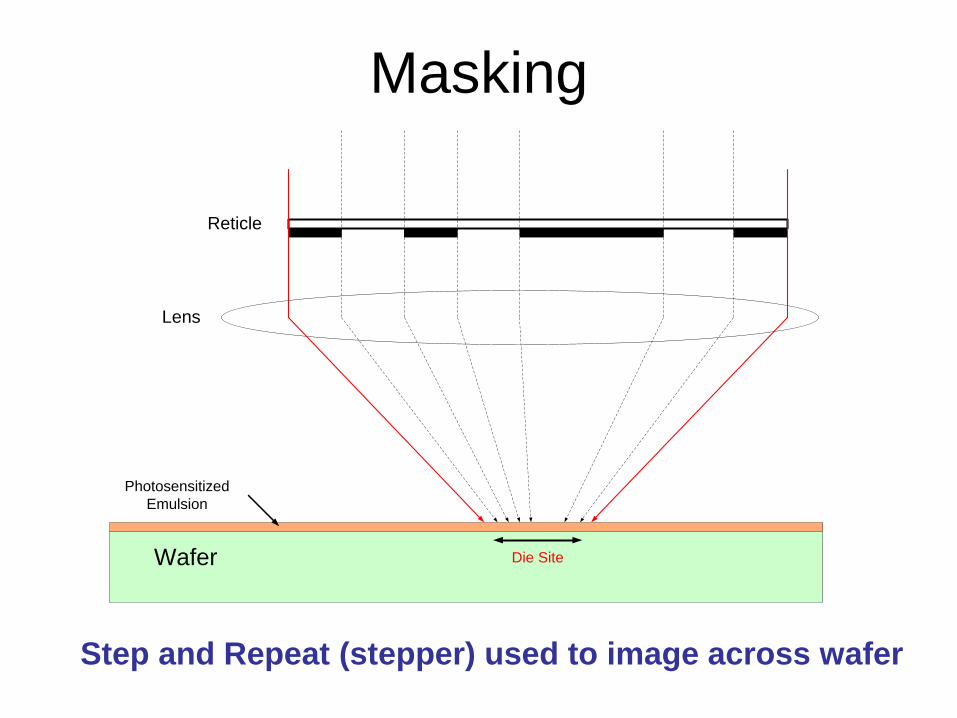
Masking
Lens
Reticle
Wafer
Photosensitized
Emulsion
Die Site
Step and Repeat (stepper) used to image across wafer

Masking Exposure through reticle

Masking
Mask Features
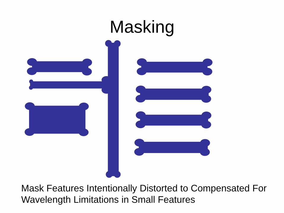
Masking
Mask Features Intentionally Distorted to Compensated For
Wavelength Limitations in Small Features
IC Fabrication Technology
• Crystal Preparation
• Masking
• Photolithographic Process
• Deposition
• Etching
• Diffusion
• Oxidation
• Epitaxy
• Polysilicon
• Contacts, Interconnect and Metalization
• Planarization
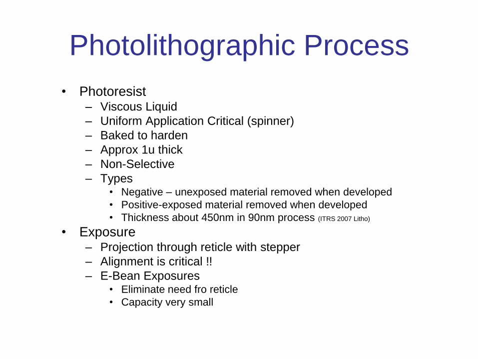
Photolithographic Process
• Photoresist – Viscous Liquid
– Uniform Application Critical (spinner)
– Baked to harden
– Approx 1u thick
– Non-Selective
– Types • Negative – unexposed material removed when developed
• Positive-exposed material removed when developed
• Thickness about 450nm in 90nm process (ITRS 2007 Litho)
• Exposure – Projection through reticle with stepper
– Alignment is critical !!
– E-Bean Exposures • Eliminate need fro reticle
• Capacity very small
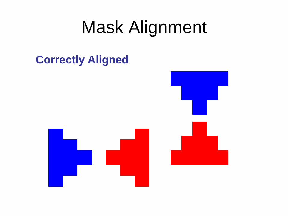
Mask Alignment
Correctly Aligned

Mask Alignment
Alignment Errors
ΔX
ΔY
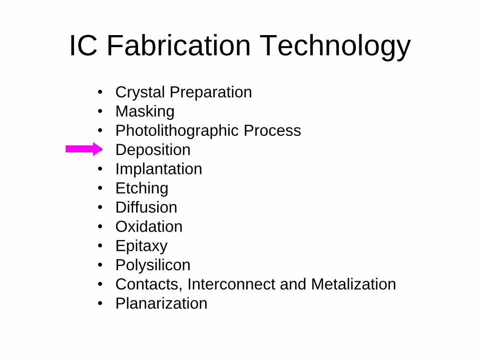
IC Fabrication Technology
• Crystal Preparation
• Masking
• Photolithographic Process
• Deposition
• Implantation
• Etching
• Diffusion
• Oxidation
• Epitaxy
• Polysilicon
• Contacts, Interconnect and Metalization
• Planarization
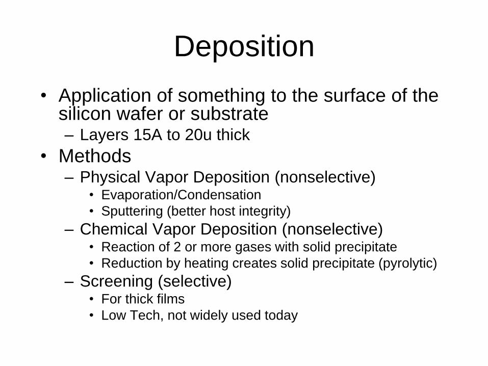
Deposition
• Application of something to the surface of the silicon wafer or substrate – Layers 15A to 20u thick
• Methods – Physical Vapor Deposition (nonselective)
• Evaporation/Condensation
• Sputtering (better host integrity)
– Chemical Vapor Deposition (nonselective) • Reaction of 2 or more gases with solid precipitate
• Reduction by heating creates solid precipitate (pyrolytic)
– Screening (selective) • For thick films
• Low Tech, not widely used today
End of Lecture 8