Embed Size (px)
Citation preview
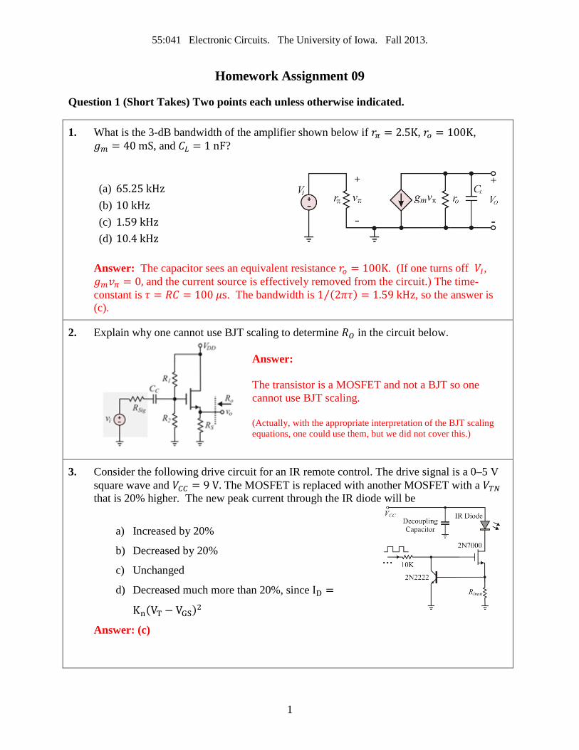
55:041 Electronic Circuits. The University of Iowa. Fall 2013.
Homework Assignment 09
Question 1 (Short Takes) Two points each unless otherwise indicated.
1. What is the 3-dB bandwidth of the amplifier shown below if 𝑟𝜋 = 2.5K, 𝑟𝑜 = 100K, 𝑔𝑚 = 40 mS, and 𝐶𝐿 = 1 nF?
(a) 65.25 kHz (b) 10 kHz (c) 1.59 kHz (d) 10.4 kHz
Answer: The capacitor sees an equivalent resistance 𝑟𝑜 = 100K. (If one turns off 𝑉𝐼, 𝑔𝑚𝑣𝜋 = 0, and the current source is effectively removed from the circuit.) The time-constant is 𝜏 = 𝑅𝐶 = 100 𝜇s. The bandwidth is 1 (2𝜋𝜏) = 1.59 kHz⁄ , so the answer is (c).
2. Explain why one cannot use BJT scaling to determine 𝑅𝑂 in the circuit below.
Answer: The transistor is a MOSFET and not a BJT so one cannot use BJT scaling. (Actually, with the appropriate interpretation of the BJT scaling equations, one could use them, but we did not cover this.)
3. Consider the following drive circuit for an IR remote control. The drive signal is a 0–5 V square wave and 𝑉𝐶𝐶 = 9 V. The MOSFET is replaced with another MOSFET with a 𝑉𝑇𝑁 that is 20% higher. The new peak current through the IR diode will be
a) Increased by 20%
b) Decreased by 20%
c) Unchanged
d) Decreased much more than 20%, since ID =
Kn(VT − VGS)2
Answer: (c)
1
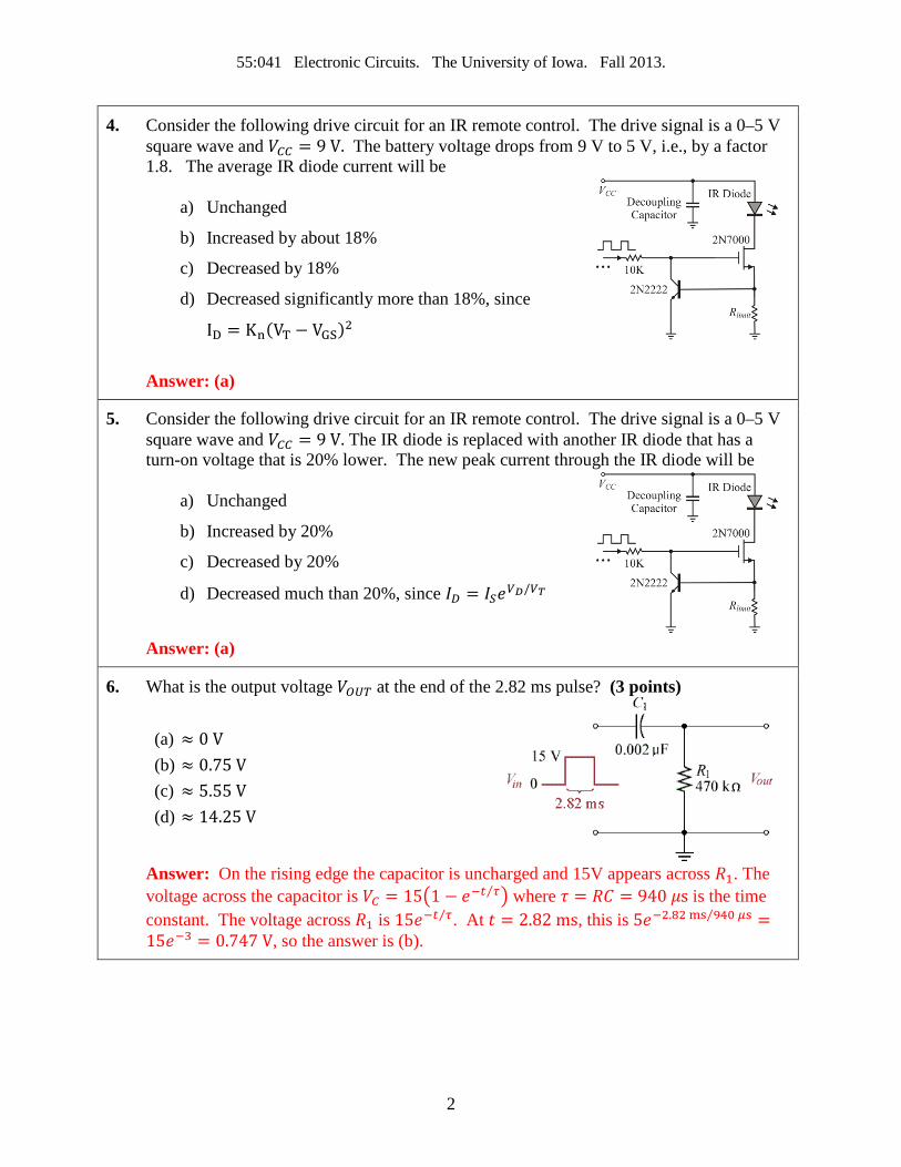
55:041 Electronic Circuits. The University of Iowa. Fall 2013.
4. Consider the following drive circuit for an IR remote control. The drive signal is a 0–5 V square wave and 𝑉𝐶𝐶 = 9 V. The battery voltage drops from 9 V to 5 V, i.e., by a factor 1.8. The average IR diode current will be
a) Unchanged
b) Increased by about 18%
c) Decreased by 18%
d) Decreased significantly more than 18%, since
ID = Kn(VT − VGS)2
Answer: (a)
5. Consider the following drive circuit for an IR remote control. The drive signal is a 0–5 V square wave and 𝑉𝐶𝐶 = 9 V. The IR diode is replaced with another IR diode that has a turn-on voltage that is 20% lower. The new peak current through the IR diode will be
a) Unchanged
b) Increased by 20%
c) Decreased by 20%
d) Decreased much than 20%, since 𝐼𝐷 = 𝐼𝑆𝑒𝑉𝐷/𝑉𝑇
Answer: (a)
6. What is the output voltage 𝑉𝑂𝑈𝑇 at the end of the 2.82 ms pulse? (3 points)
(a) ≈ 0 V (b) ≈ 0.75 V (c) ≈ 5.55 V (d) ≈ 14.25 V
Answer: On the rising edge the capacitor is uncharged and 15V appears across 𝑅1. The voltage across the capacitor is 𝑉𝐶 = 15�1 − 𝑒−𝑡 𝜏⁄ � where 𝜏 = 𝑅𝐶 = 940 𝜇s is the time constant. The voltage across 𝑅1 is 15𝑒−𝑡 𝜏⁄ . At 𝑡 = 2.82 ms, this is 5𝑒−2.82 ms 940 𝜇s⁄ =15𝑒−3 = 0.747 V, so the answer is (b).
2
55:041 Electronic Circuits. The University of Iowa. Fall 2013.
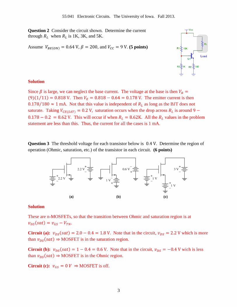
Question 2 Consider the circuit shown. Determine the current through 𝑅𝐿 when 𝑅𝐿 is 1K, 3K, and 5K. Assume 𝑉𝐵𝐸(𝑂𝑁) = 0.64 V, 𝛽 = 200, and 𝑉𝐶𝐶 = 9 V. (5 points)
Solution
Since 𝛽 is large, we can neglect the base current. The voltage at the base is then 𝑉𝐵 =(9)(1 11⁄ ) = 0.818 V. Then 𝑉𝐸 = 0.818 − 0.64 = 0.178 V. The emitter current is then 0.178 180⁄ ≈ 1 mA. Not that this value is independent of 𝑅𝐿 as long as the BJT does not saturate. Taking 𝑉𝐶𝐸(𝑆𝐴𝑇) = 0.2 V, saturation occurs when the drop across 𝑅𝐿 is around 9 −0.178 − 0.2 = 8.62 V. This will occur if when 𝑅𝐿 = 8.62K. All the 𝑅𝐿 values in the problem statement are less than this. Thus, the current for all the cases is 1 mA.
Question 3 The threshold voltage for each transistor below is 0.4 V. Determine the region of operation (Ohmic, saturation, etc.) of the transistor in each circuit. (6 points)
Solution
These are n-MOSFETs, so that the transition between Ohmic and saturation region is at 𝑣𝐷𝑆(𝑠𝑎𝑡) = 𝑣𝐺𝑆 − 𝑉𝑇𝑁.
Circuit (a): 𝑣𝐷𝑆(𝑠𝑎𝑡) = 2.0 − 0.4 = 1.8 V. Note that in the circuit, 𝑣𝐷𝑆 = 2.2 V which is more than 𝑣𝐷𝑆(𝑠𝑎𝑡) ⇒ MOSFET is in the saturation region.
Circuit (b): 𝑣𝐷𝑆(𝑠𝑎𝑡) = 1 − 0.4 = 0.6 V. Note that in the circuit, 𝑣𝐷𝑆 = −0.4 V wich is less than 𝑣𝐷𝑆(𝑠𝑎𝑡) ⇒ MOSFET is in the Ohmic region.
Circuit (c): 𝑣𝐺𝑆 = 0 𝑉 ⇒ MOSFET is off.
3
55:041 Electronic Circuits. The University of Iowa. Fall 2013.
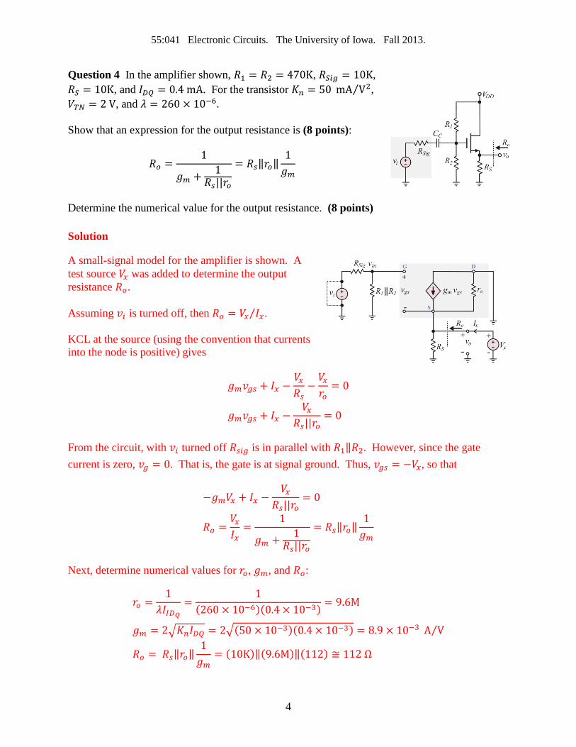
Question 4 In the amplifier shown, 𝑅1 = 𝑅2 = 470K, 𝑅𝑆𝑖𝑔 = 10K, 𝑅𝑆 = 10K, and 𝐼𝐷𝑄 = 0.4 mA. For the transistor 𝐾𝑛 = 50 mA V2⁄ , 𝑉𝑇𝑁 = 2 V, and 𝜆 = 260 × 10−6. Show that an expression for the output resistance is (8 points):
𝑅𝑜 =1
𝑔𝑚 + 1𝑅𝑠||𝑟𝑜
= 𝑅𝑠‖𝑟𝑜‖1𝑔𝑚
Determine the numerical value for the output resistance. (8 points)
Solution
A small-signal model for the amplifier is shown. A test source 𝑉𝑥 was added to determine the output resistance 𝑅𝑜. Assuming 𝑣𝑖 is turned off, then 𝑅𝑜 = 𝑉𝑥 𝐼𝑥⁄ . KCL at the source (using the convention that currents into the node is positive) gives
𝑔𝑚𝑣𝑔𝑠 + 𝐼𝑥 −𝑉𝑥𝑅𝑠
−𝑉𝑥𝑟𝑜
= 0
𝑔𝑚𝑣𝑔𝑠 + 𝐼𝑥 −𝑉𝑥
𝑅𝑠||𝑟𝑜= 0
From the circuit, with 𝑣𝑖 turned off 𝑅𝑠𝑖𝑔 is in parallel with 𝑅1‖𝑅2. However, since the gate current is zero, 𝑣𝑔 = 0. That is, the gate is at signal ground. Thus, 𝑣𝑔𝑠 = −𝑉𝑥, so that
−𝑔𝑚𝑉𝑥 + 𝐼𝑥 −𝑉𝑥
𝑅𝑠||𝑟𝑜= 0
𝑅𝑜 =𝑉𝑥𝐼𝑥
=1
𝑔𝑚 + 1𝑅𝑠||𝑟𝑜
= 𝑅𝑠‖𝑟𝑜‖1𝑔𝑚
Next, determine numerical values for 𝑟𝑜, 𝑔𝑚, and 𝑅𝑜:
𝑟𝑜 =1
𝜆𝐼𝐼𝐷𝑄=
1(260 × 10−6)(0.4 × 10⁻³) = 9.6M
𝑔𝑚 = 2�𝐾𝑛𝐼𝐷𝑄 = 2�(50 × 10−3)(0.4 × 10⁻³) = 8.9 × 10⁻³ A V⁄
𝑅𝑜 = 𝑅𝑠‖𝑟𝑜‖1𝑔𝑚
= (10K)‖(9.6M)‖(112) ≅ 112 Ω
4
55:041 Electronic Circuits. The University of Iowa. Fall 2013.
Checking results with SPICE (Not Required)
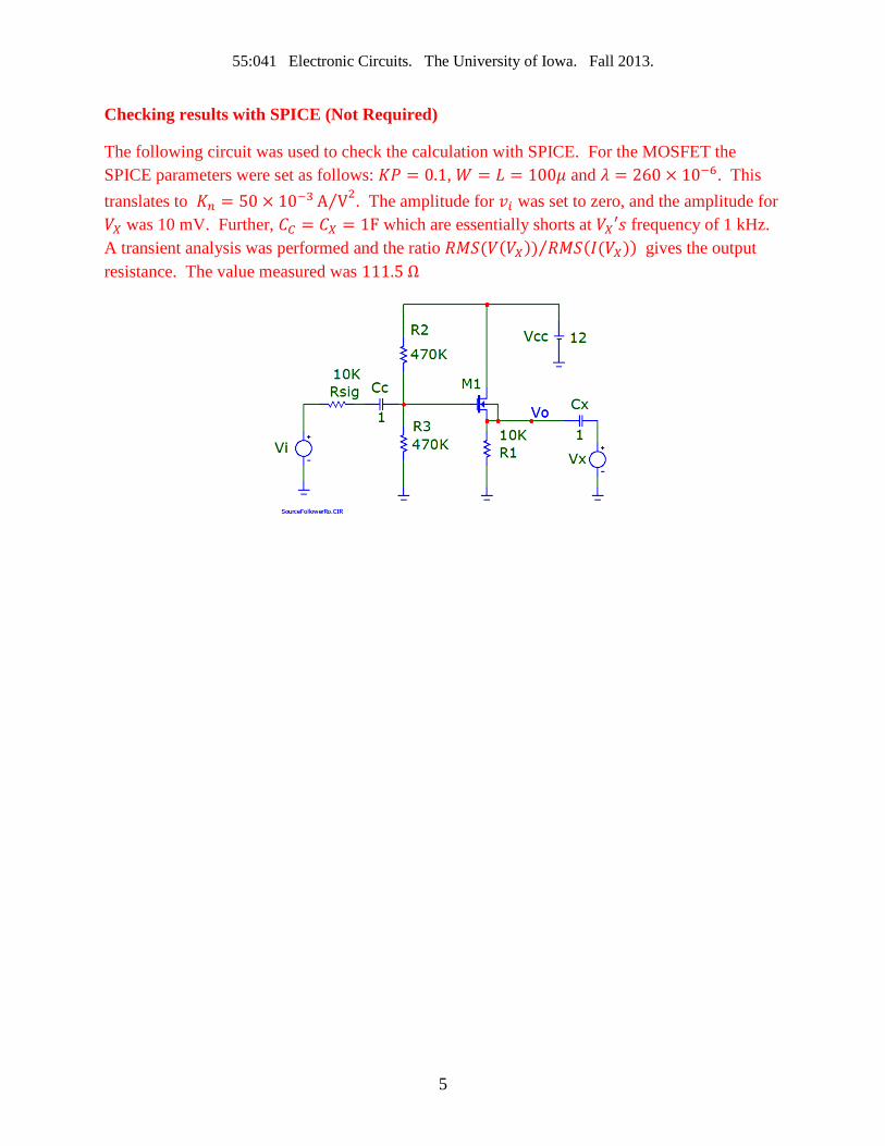
The following circuit was used to check the calculation with SPICE. For the MOSFET the SPICE parameters were set as follows: 𝐾𝑃 = 0.1, 𝑊 = 𝐿 = 100𝜇 and 𝜆 = 260 × 10−6. This translates to 𝐾𝑛 = 50 × 10−3 A V⁄ 2. The amplitude for 𝑣𝑖 was set to zero, and the amplitude for 𝑉𝑋 was 10 mV. Further, 𝐶𝐶 = 𝐶𝑋 = 1F which are essentially shorts at 𝑉𝑋′𝑠 frequency of 1 kHz. A transient analysis was performed and the ratio 𝑅𝑀𝑆(𝑉(𝑉𝑋)) 𝑅𝑀𝑆(𝐼(𝑉𝑋))⁄ gives the output resistance. The value measured was 111.5 Ω
5
55:041 Electronic Circuits. The University of Iowa. Fall 2013.
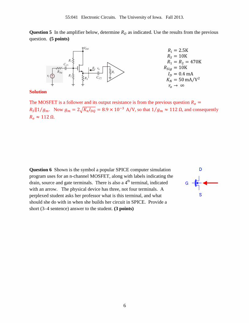
Question 5 In the amplifier below, determine 𝑅𝑂 as indicated. Use the results from the previous question. (5 points)
𝑅𝑖 = 2.5K 𝑅𝑆 = 10K 𝑅1 = 𝑅2 = 470K
𝑅𝑆𝑖𝑔 = 10K 𝐼𝐷 = 0.4 mA 𝐾𝑁 = 50 mA V2⁄ 𝑟𝑜 → ∞
Solution
The MOSFET is a follower and its output resistance is from the previous question 𝑅𝑜 =𝑅𝑆‖1 𝑔𝑚⁄ . Now 𝑔𝑚 = 2�𝐾𝑛𝐼𝐷𝑄 = 8.9 × 10⁻³ A V⁄ , so that 1 𝑔𝑚 ≈ 112 Ω⁄ , and consequently 𝑅𝑜 ≈ 112 Ω.
Question 6 Shown is the symbol a popular SPICE computer simulation program uses for an n-channel MOSFET, along with labels indicating the drain, source and gate terminals. There is also a 4th terminal, indicated with an arrow. The physical device has three, not four terminals. A perplexed student asks her professor what is this terminal, and what should she do with in when she builds her circuit in SPICE. Provide a short (3–4 sentence) answer to the student. (3 points)
6
55:041 Electronic Circuits. The University of Iowa. Fall 2013.
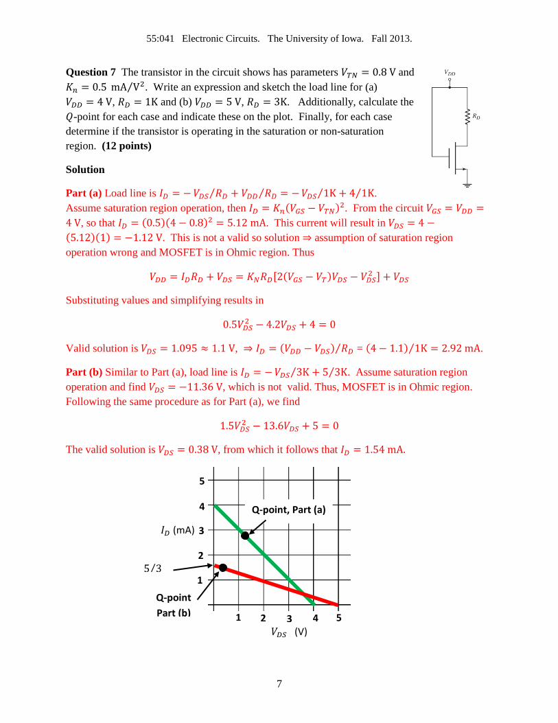
Question 7 The transistor in the circuit shows has parameters 𝑉𝑇𝑁 = 0.8 V and 𝐾𝑛 = 0.5 mA V2⁄ . Write an expression and sketch the load line for (a) 𝑉𝐷𝐷 = 4 V, 𝑅𝐷 = 1K and (b) 𝑉𝐷𝐷 = 5 V, 𝑅𝐷 = 3K. Additionally, calculate the 𝑄-point for each case and indicate these on the plot. Finally, for each case determine if the transistor is operating in the saturation or non-saturation region. (12 points)
Solution
Part (a) Load line is 𝐼𝐷 = −𝑉𝐷𝑆 𝑅𝐷⁄ + 𝑉𝐷𝐷 𝑅𝐷⁄ = −𝑉𝐷𝑆 1K⁄ + 4 1K⁄ . Assume saturation region operation, then 𝐼𝐷 = 𝐾𝑛(𝑉𝐺𝑆 − 𝑉𝑇𝑁)2. From the circuit 𝑉𝐺𝑆 = 𝑉𝐷𝐷 =4 V, so that 𝐼𝐷 = (0.5)(4 − 0.8)2 = 5.12 mA. This current will result in 𝑉𝐷𝑆 = 4 −(5.12)(1) = −1.12 V. This is not a valid so solution ⇒ assumption of saturation region operation wrong and MOSFET is in Ohmic region. Thus
𝑉𝐷𝐷 = 𝐼𝐷𝑅𝐷 + 𝑉𝐷𝑆 = 𝐾𝑁𝑅𝐷[2(𝑉𝐺𝑆 − 𝑉𝑇)𝑉𝐷𝑆 − 𝑉𝐷𝑆2 ] + 𝑉𝐷𝑆
Substituting values and simplifying results in
0.5𝑉𝐷𝑆2 − 4.2𝑉𝐷𝑆 + 4 = 0
Valid solution is 𝑉𝐷𝑆 = 1.095 ≈ 1.1 V, ⇒ 𝐼𝐷 = (𝑉𝐷𝐷 − 𝑉𝐷𝑆) 𝑅𝐷⁄ = (4 − 1.1) 1K⁄ = 2.92 mA.
Part (b) Similar to Part (a), load line is 𝐼𝐷 = −𝑉𝐷𝑆 3K⁄ + 5 3K⁄ . Assume saturation region operation and find 𝑉𝐷𝑆 = −11.36 V, which is not valid. Thus, MOSFET is in Ohmic region. Following the same procedure as for Part (a), we find
1.5𝑉𝐷𝑆2 − 13.6𝑉𝐷𝑆 + 5 = 0
The valid solution is 𝑉𝐷𝑆 = 0.38 V, from which it follows that 𝐼𝐷 = 1.54 mA.
1 2 3 4 5
𝑉𝐷𝑆 (V)
1
2
3
4
5
𝐼𝐷 (mA)
5 3⁄
Q-point, Part (a)
Q-point Part (b)
7
55:041 Electronic Circuits. The University of Iowa. Fall 2013.
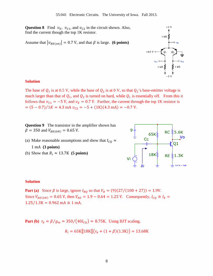
Question 8 Find 𝑣𝐸 , 𝑣𝐶1, and 𝑣𝐶2 in the circuit shown. Also, find the current though the top 1K resistor. Assume that �𝑣𝐵𝐸(𝑜𝑛)� = 0.7 V, and that 𝛽 is large. (6 points)
Solution
The base of 𝑄1 is at 0.5 V, while the base of 𝑄2 is at 0 V, so that 𝑄2’s base-emitter voltage is much larger than that of 𝑄1, and 𝑄2 is turned on hard, while 𝑄1 is essentially off. From this it follows that 𝑣𝐶1 = −5 V, and 𝑣𝐸 = 0.7 V. Further, the current through the top 1K resistor is = (5 − 0.7) 1𝐾⁄ = 4.3 mA 𝑣𝐶2 = −5 + (1K)(4.3 mA) = −0.7 V.
Question 9 The transistor in the amplifier shown has 𝛽 = 350 and 𝑉𝐵𝐸(𝑂𝑁) = 0.65 V. (a) Make reasonable assumptions and show that 𝐼𝐶𝑄 ≈
1 mA (3 points) (b) Show that 𝑅𝑖 ≈ 13.7K (5 points)
Solution
Part (a) Since 𝛽 is large, ignore 𝐼𝐵𝑄 so that 𝑉𝐵 = (9)(27 (100 + 27)⁄ ) = 1.9V. Since 𝑉𝐵𝐸(𝑂𝑁) = 0.65 V, then 𝑉𝑅𝐸 = 1.9 − 0.64 = 1.25 V. Consequently, 𝐼𝐶𝑄 ≅ 𝐼𝐸 =1.25 1.3K = 0.962 mA ≅ 1 mA⁄ .
Part (b) 𝑟𝜋 = 𝛽 𝑔𝑚 = 350 �40𝐼𝐶𝑄� =⁄⁄ 8.75K. Using BJT scaling,
𝑅𝑖 = 65K�18K��𝑟𝜋 + (1 + 𝛽)(1.3K)� = 13.68K
8
55:041 Electronic Circuits. The University of Iowa. Fall 2013.
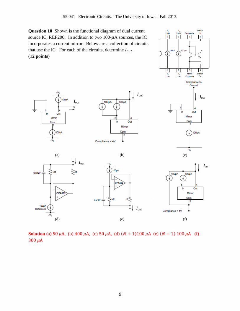
Question 10 Shown is the functional diagram of dual current source IC, REF200. In addition to two 100-𝜇A sources, the IC incorporates a current mirror. Below are a collection of circuits that use the IC. For each of the circuits, determine 𝐼𝑜𝑢𝑡. (12 points)
(a) (b) (c)
(d) (e) (f)
Solution (a) 50 𝜇A, (b) 400 𝜇A, (c) 50 𝜇A, (d) (𝑁 + 1)100 𝜇A (e) (𝑁 + 1) 100 𝜇A (f) 300 𝜇A
Iout Iout Iout
Iout
Iout
Iout
9

55:041 Electronic Circuits. The University of Iowa. Fall 2013.
Question 11 Consider the amplifier below, which amplifies the signal from a sensor with an internal resistance of 1K. Ignore BJT’s output resistance, and assume 𝐶1 = 𝐶2 = 𝐶3 → ∞.
𝛽 = 100 𝐼𝐶 = 0.245 mA
(a) Determine 𝑔𝑚, 𝑟𝜋 (4 points) (b) Using BJT scaling, determine 𝑅𝑖—see figure (4 points) (c) Using the ratio of the collector and emitter resistors, estimate the overall voltage gain
𝐴𝑣 = 𝑣𝑜 𝑣𝑠⁄ (4 points) (d) Calculate the voltage gain 𝐴𝑣 = 𝑣𝑜 𝑣𝑠⁄ , but do not use the approximation that involves the
ratio of the collector and emitter resistors, but rather incorporate the 𝛽 of the transistor (4 points)
Solution Part (a)
𝑔𝑚 = 40 𝐼𝐶 = 9.8 mS, 𝑟𝜋 =𝛽𝑔𝑚
= 10.2 K
Part (b)
𝑅𝑖 = 𝑅1�|𝑅2|�[𝑟𝜋 + (1 + 𝛽)𝑅𝐸] = 300K�|160K|�[10.2K + 101 × 3K] = 78.3K Part (c) The effective collector resistance is 𝑅𝐶′ = 22K||100K = 18K and the sensor’s internal resistance and 𝑅𝑖 form a voltage divider. Thus
𝐴𝑣 =𝑣𝑜𝑣𝑠≅ −
𝑅𝑖𝑅𝑆 + 𝑅𝑖
𝑅𝐶′
𝑅𝐸= −
78.31 + 78.3
18K3K
= −5.93
10
55:041 Electronic Circuits. The University of Iowa. Fall 2013.
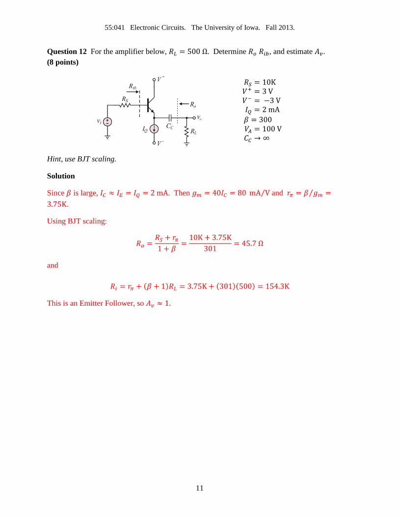
Question 12 For the amplifier below, 𝑅𝐿 = 500 Ω. Determine 𝑅𝑜 𝑅𝑖𝑏, and estimate 𝐴𝑣. (8 points)
𝑅𝑆 = 10K 𝑉+ = 3 V 𝑉− = −3 V 𝐼𝑄 = 2 mA 𝛽 = 300 𝑉𝐴 = 100 V 𝐶𝐶 → ∞
Hint, use BJT scaling.
Solution
Since 𝛽 is large, 𝐼𝐶 ≈ 𝐼𝐸 = 𝐼𝑄 = 2 mA. Then 𝑔𝑚 = 40𝐼𝐶 = 80 mA V⁄ and 𝑟𝜋 = 𝛽 𝑔𝑚⁄ =3.75K.
Using BJT scaling:
𝑅𝑜 =𝑅𝑆 + 𝑟𝜋1 + 𝛽
=10K + 3.75K
301= 45.7 Ω
and
𝑅𝑖 = 𝑟𝜋 + (𝛽 + 1)𝑅𝐿 = 3.75K + (301)(500) = 154.3K
This is an Emitter Follower, so 𝐴𝑣 ≈ 1.
11
55:041 Electronic Circuits. The University of Iowa. Fall 2013.
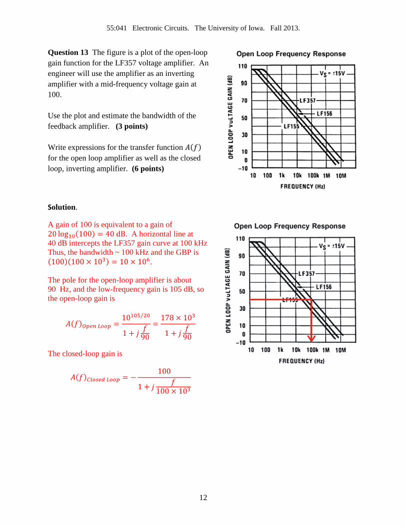
Question 13 The figure is a plot of the open-loop gain function for the LF357 voltage amplifier. An engineer will use the amplifier as an inverting amplifier with a mid-frequency voltage gain at 100. Use the plot and estimate the bandwidth of the feedback amplifier. (3 points) Write expressions for the transfer function 𝐴(𝑓) for the open loop amplifier as well as the closed loop, inverting amplifier. (6 points)
Solution.
A gain of 100 is equivalent to a gain of 20 log10(100) = 40 dB. A horizontal line at 40 dB intercepts the LF357 gain curve at 100 kHz Thus, the bandwidth ~ 100 kHz and the GBP is (100)(100 × 103) = 10 × 106. The pole for the open-loop amplifier is about 90 Hz, and the low-frequency gain is 105 dB, so the open-loop gain is
𝐴(𝑓)𝑂𝑝𝑒𝑛 𝐿𝑜𝑜𝑝 =10105 20⁄
1 + 𝑗 𝑓90
=178 × 103
1 + 𝑗 𝑓90
The closed-loop gain is
𝐴(𝑓)𝐶𝑙𝑜𝑠𝑒𝑑 𝐿𝑜𝑜𝑝 = −100
1 + 𝑗 𝑓100 × 103
12
55:041 Electronic Circuits. The University of Iowa. Fall 2013.
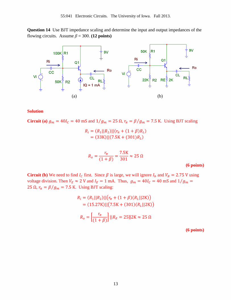
Question 14 Use BJT impedance scaling and determine the input and output impedances of the flowing circuits. Assume β = 300. (12 points)
(a) (b)
Solution
Circuit (a) 𝑔𝑚 = 40𝐼𝐶 = 40 mS and 1 𝑔𝑚⁄ = 25 Ω, 𝑟𝜋 = 𝛽 𝑔𝑚 = 7.5 K⁄ . Using BJT scaling
𝑅𝑖 = (𝑅1||𝑅2)||(𝑟𝜋 + (1 + 𝛽)𝑅𝐿) = (33K)||(7.5K + (301)𝑅𝐿)
𝑅𝑜 =𝑟𝜋
(1 + 𝛽)=
7.5K301
≈ 25 Ω
(6 points)
Circuit (b) We need to find 𝐼𝐶 first. Since 𝛽 is large, we will ignore 𝐼𝑏 and 𝑉𝐵 = 2.75 V using voltage division. Then 𝑉𝐸 ≈ 2 V and 𝐼𝐸 = 1 mA. Thus, 𝑔𝑚 = 40𝐼𝐶 = 40 mS and 1 𝑔𝑚⁄ =25 Ω, 𝑟𝜋 = 𝛽 𝑔𝑚 = 7.5 K⁄ . Using BJT scaling:
𝑅𝑖 = (𝑅1||𝑅2)||�𝑟𝜋 + (1 + 𝛽)(𝑅𝐿||2K)� = (15.27K)||�7.5K + (301)(𝑅𝐿||2K)�
𝑅𝑜 = �𝑟𝜋
(1 + 𝛽)� ||𝑅𝐸 = 25‖2K ≈ 25 Ω
(6 points)
13
55:041 Electronic Circuits. The University of Iowa. Fall 2013.
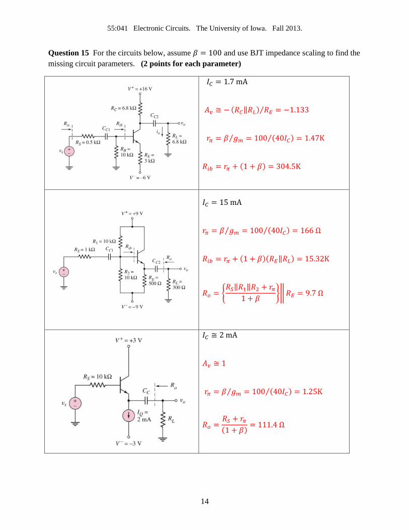
Question 15 For the circuits below, assume 𝛽 = 100 and use BJT impedance scaling to find the missing circuit parameters. (2 points for each parameter)
𝐼𝐶 = 1.7 mA
𝐴𝑣 ≅ − (𝑅𝐶‖𝑅𝐿) 𝑅𝐸 = −1.133⁄
𝑟𝜋 = 𝛽 𝑔𝑚 = 100 (40𝐼𝐶) = 1.47K⁄⁄
𝑅𝑖𝑏 = 𝑟𝜋 + (1 + 𝛽) = 304.5K
𝐼𝐶 = 15 mA
𝑟𝜋 = 𝛽 𝑔𝑚 = 100 (40𝐼𝐶) = 166 Ω⁄⁄
𝑅𝑖𝑏 = 𝑟𝜋 + (1 + 𝛽)(𝑅𝐸‖𝑅𝐿) = 15.32K
𝑅𝑜 = �𝑅𝑆‖𝑅1‖𝑅2 + 𝑟𝜋
1 + 𝛽��𝑅𝐸 = 9.7 Ω
𝐼𝐶 ≅ 2 mA
𝐴𝑣 ≅ 1
𝑟𝜋 = 𝛽 𝑔𝑚 = 100 (40𝐼𝐶) = 1.25K⁄⁄
𝑅𝑜 =𝑅𝑆 + 𝑟𝜋(1 + 𝛽) = 111.4 Ω
14