Embed Size (px)
Citation preview
8/9/2019 Group Delay Designcon2006
http://slidepdf.com/reader/full/group-delay-designcon2006 1/23
DesignCon 2006
Group Delay and its Impact onSerial Data Transmission and
Testing
Peter J. Pupalaikis, LeCroy Corporation

8/9/2019 Group Delay Designcon2006
http://slidepdf.com/reader/full/group-delay-designcon2006 2/23
AbstractThis paper is an extension of last years paper entitled “Eye Pattern Measurements in Scopes”.
Last years paper pointed out the effects of bandwidth, roll-off rate, flatness, and group delay
characteristics along with probe loading and return-loss. It only glossed over the more
complicated topic of phase response and group delay. This paper goes into greater detail on thistopic and explains what group delay is, what its impact is, what theoretically correct group delay
is, and how group delay is compensated in both serial data test equipment and serial datatransmitters and receivers.
Author(s) BiographyPete Pupalaikis is Principal Technologist at LeCroy working on new technology development.
Previously he was Product Marketing Manager for high-end scopes. He has six patents in the
design of measurement instruments. He holds a BSEE from Rutgers University and is a memberof Tau Beta Pi, Eta Kappa Nu and the IEEE Signal Processing and Communications Societies.
8/9/2019 Group Delay Designcon2006
http://slidepdf.com/reader/full/group-delay-designcon2006 3/23
1
IntroductionLast year, I presented a paper entitled “Eye Patterns in Scopes”. That paper covered many topicsrelated to serial data characteristics, mainly bit-rate and rise-time and oscilloscope characteristics
such as bandwidth, roll-off rate, flatness, phase response, etc. The paper explained how the
characteristics interact to determine what you see on your scope screen when measuring eye-
patterns.
The topic of phase response (or group delay response – I’ll use these interchangeably) was briefly introduced. Group delay, while more complicated to understand and compensate than its
brother magnitude response, is equally important.
The first part of this paper deals with oscilloscope responses. I will discuss linear phase systemsand minimum phase systems and contrast the two. I will discuss allpass filters and how they
work. I will explain how linear phase and minimum phase systems are related by allpass filter
networks. I will also explain minimum phase systems from a zero location standpoint and showyou how to make minimum phase systems out of any impulse response. I will show the
difference between the two response characteristics where serial data measurement is concernedand show why linear phase might be preferable in this case.
The second part of this paper deals with channel group delay characteristics and how these affect
serial data transmission. I will show a simple simulation along with a very simple model forunderstanding the primary effect of group delay on the eye. I will briefly discuss how group
delay equalization can be implemented in hardware.
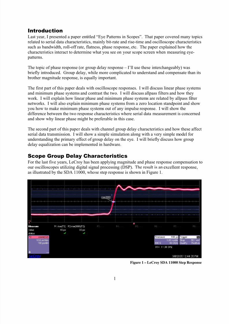
Scope Group Delay CharacteristicsFor the last five years, LeCroy has been applying magnitude and phase response compensation to
our oscilloscopes utilizing digital signal processing (DSP). The result is an excellent response,as illustrated by the SDA 11000, whose step response is shown in Figure 1.
Figure 1 – LeCroy SDA 11000 Step Response
8/9/2019 Group Delay Designcon2006
http://slidepdf.com/reader/full/group-delay-designcon2006 4/23
2
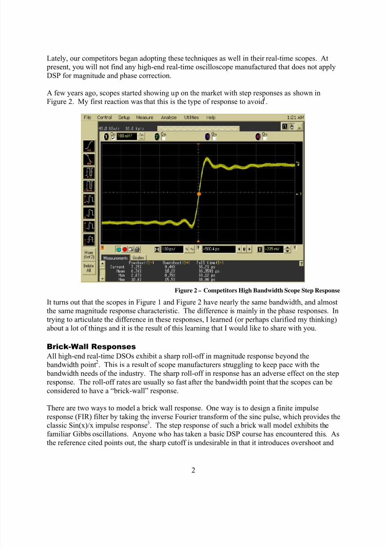
Lately, our competitors began adopting these techniques as well in their real-time scopes. At present, you will not find any high-end real-time oscilloscope manufactured that does not apply
DSP for magnitude and phase correction.
A few years ago, scopes started showing up on the market with step responses as shown inFigure 2. My first reaction was that this is the type of response to avoid 1.
Figure 2 – Competitors High Bandwidth Scope Step Response
It turns out that the scopes in Figure 1 and Figure 2 have nearly the same bandwidth, and almostthe same magnitude response characteristic. The difference is mainly in the phase responses. In
trying to articulate the difference in these responses, I learned (or perhaps clarified my thinking)
about a lot of things and it is the result of this learning that I would like to share with you.
Brick-Wall Responses
All high-end real-time DSOs exhibit a sharp roll-off in magnitude response beyond the bandwidth point
2. This is a result of scope manufacturers struggling to keep pace with the
bandwidth needs of the industry. The sharp roll-off in response has an adverse effect on the step
response. The roll-off rates are usually so fast after the bandwidth point that the scopes can beconsidered to have a “brick-wall” response.
There are two ways to model a brick wall response. One way is to design a finite impulse
response (FIR) filter by taking the inverse Fourier transform of the sinc pulse, which provides theclassic Sin(x)/x impulse response
3. The step response of such a brick wall model exhibits the
familiar Gibbs oscillations. Anyone who has taken a basic DSP course has encountered this. As
the reference cited points out, the sharp cutoff is undesirable in that it introduces overshoot and
8/9/2019 Group Delay Designcon2006
http://slidepdf.com/reader/full/group-delay-designcon2006 5/23
3
ringing, but this is unavoidable when the scope runs out of response. But he also points out that
were it not for the delay, the response would appear to have an instantaneous step response withanticipatory ripples – a violation of real-world causality.
Another way to model a brick wall response is to create a Butterworth filter and design it with
ever increasing filter order – by introducing more poles
4
. In the limit, this filter takes on the brick wall response, but you will note that this system never preshoots.
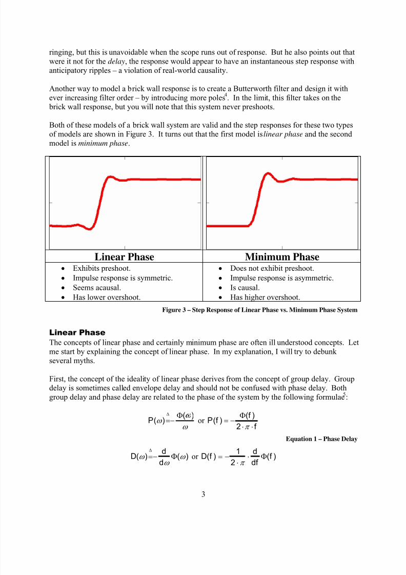
Both of these models of a brick wall system are valid and the step responses for these two typesof models are shown in Figure 3. It turns out that the first model is linear phase and the second
model is minimum phase.
Linear Phase Minimum Phase• Exhibits preshoot.
• Impulse response is symmetric.
• Seems acausal.
• Has lower overshoot.
• Does not exhibit preshoot.
• Impulse response is asymmetric.
• Is causal.
• Has higher overshoot.
Figure 3 – Step Response of Linear Phase vs. Minimum Phase System
Linear Phase
The concepts of linear phase and certainly minimum phase are often ill understood concepts. Let
me start by explaining the concept of linear phase. In my explanation, I will try to debunkseveral myths.
First, the concept of the ideality of linear phase derives from the concept of group delay. Groupdelay is sometimes called envelope delay and should not be confused with phase delay. Both
group delay and phase delay are related to the phase of the system by the following formulae5:
ω ω
)()( Φ−=
∆
P orf
f f P
⋅⋅
Φ−=
π 2
)()(
Equation 1 – Phase Delay
)()( ω ω
ω Φ−=∆
d
dD or )(
2
1)( f
df
df D Φ⋅
⋅−=
π

8/9/2019 Group Delay Designcon2006
http://slidepdf.com/reader/full/group-delay-designcon2006 6/23
4
Equation 2 – Group Delay
The phase delay is the time delay of a sinusoid at frequency f assuming that the sinusoid is
constant for all time. The group delay is the time delay of the amplitude envelope of a narrow
group of frequencies around f. You can see that when the phase )(f Φ is linear with frequency,
both the phase delay and the group delay evaluate to a constant delay. When the phase is non-
linear with frequency, neither the phase delay nor group delay is constant with frequency.
In a typically encountered band-limited system, the group delay rises near the band edge. The
reason for this is that the band edge is defined by the presence of one or more poles that, whileadding 20 dB/decade to the roll-off rate, also add 90 degrees of phase lag. At the center
frequency of a complex conjugate pair of poles, where the magnitude response tends to be
peaked, the group delay is also peaked. This means that high frequency components of the
system tend to be delayed as they pass through the system. This shows up in the step response asa slower risetime and higher overshoot since the high frequency components don’t arrivecoincident with the edge but instead arrive after the edge has passed.
Most of us have been taught in school that linear phase is the desired phase response. In audioand to some extent, communications systems, this is true. In control systems, this is not true.
Myth: Linear phase describes the ideal phase response much as flat describes the ideal
magnitude response.
I call this a myth because it fails to consider one point:
It is impossible to band-limit a response without introducing delay.
It is impossible to linearize the phase of a band-limited system without adding more delay.
The delay of the linear phase system is sometimes intolerable. To illustrate the situation,consider the step in Figure 3. The step on the right was generated using a 5
th order Butterworth
filter. A Butterworth filter is an all-pole filter and is therefore infinite impulse response (IIR) as
poles mean that the output depends not only on the input but on some internal storage elementthat theoretically remembers its past history forever. The step on the left is linear phase and
looks like it was generated using the Sin(x)/x FIR filter. This is not true, however, and I can’t
help debunking another common myth:
Myth: FIR filters are linear phase, IIR filters are not.
Reality is:
It is easy to design linear phase FIR filters. It is not easy to design linear phase IIR filters.
And the corollary: It is not easy to design minimum phase FIR filters.
It is easy to design minimum phase IIR filters.
Of course some of you who are experienced in filter design may quibble with these statements.
Forgive me if there is some exaggeration here.
8/9/2019 Group Delay Designcon2006
http://slidepdf.com/reader/full/group-delay-designcon2006 7/23
5
The reality is that most FIR filters designed directly as FIRs are linear phase because you have achoice of what you want to set the phase to, and most often, the choice made is linear phase.
Similarly, there is some elegance to a symmetric FIR (one that is symmetric on both sides about
some center peak in the impulse response) – the symmetry imposes linear phase. IIR filters are
usually designed using analog filter design techniques. Most analog filters are all-pole and will be minimum phase (or certainly not linear phase) unless you do something special.
Allpass Filters
The step response shown at the left in Figure 3 is actually the 5th
order Butterworth filter shown
to the right with the addition of a phase compensation network designed to linearize the phase.
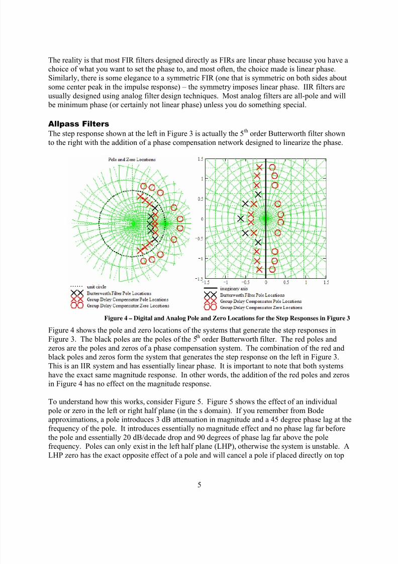
Figure 4 – Digital and Analog Pole and Zero Locations for the Step Responses in Figure 3
Figure 4 shows the pole and zero locations of the systems that generate the step responses in
Figure 3. The black poles are the poles of the 5th
order Butterworth filter. The red poles and
zeros are the poles and zeros of a phase compensation system. The combination of the red and black poles and zeros form the system that generates the step response on the left in Figure 3.
This is an IIR system and has essentially linear phase. It is important to note that both systems
have the exact same magnitude response. In other words, the addition of the red poles and zerosin Figure 4 has no effect on the magnitude response.
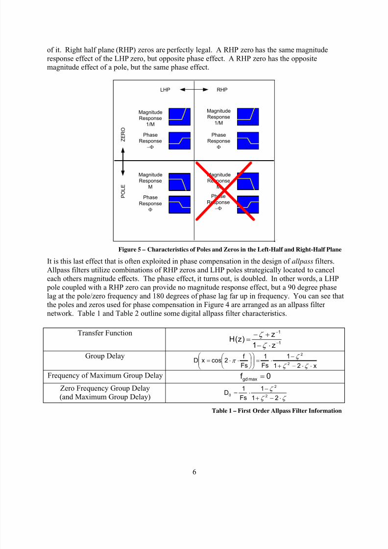
To understand how this works, consider Figure 5. Figure 5 shows the effect of an individual
pole or zero in the left or right half plane (in the s domain). If you remember from Bodeapproximations, a pole introduces 3 dB attenuation in magnitude and a 45 degree phase lag at the
frequency of the pole. It introduces essentially no magnitude effect and no phase lag far before
the pole and essentially 20 dB/decade drop and 90 degrees of phase lag far above the polefrequency. Poles can only exist in the left half plane (LHP), otherwise the system is unstable. A
LHP zero has the exact opposite effect of a pole and will cancel a pole if placed directly on top
8/9/2019 Group Delay Designcon2006
http://slidepdf.com/reader/full/group-delay-designcon2006 8/23
6
of it. Right half plane (RHP) zeros are perfectly legal. A RHP zero has the same magnitude
response effect of the LHP zero, but opposite phase effect. A RHP zero has the oppositemagnitude effect of a pole, but the same phase effect.
LHP RHP
P O
L E
Z E R O
Magnitude
Response
M
Phase
Response
Φ
Magnitude
Response
M
Phase
Response
−Φ
Magnitude
Response
1/M
Phase
Response
−Φ
Phase
Response
Φ
Magnitude
Response
1/M
Figure 5 – Characteristics of Poles and Zeros in the Left-Half and Right-Half Plane
It is this last effect that is often exploited in phase compensation in the design of allpass filters.
Allpass filters utilize combinations of RHP zeros and LHP poles strategically located to canceleach others magnitude effects. The phase effect, it turns out, is doubled. In other words, a LHP
pole coupled with a RHP zero can provide no magnitude response effect, but a 90 degree phaselag at the pole/zero frequency and 180 degrees of phase lag far up in frequency. You can see thatthe poles and zeros used for phase compensation in Figure 4 are arranged as an allpass filter
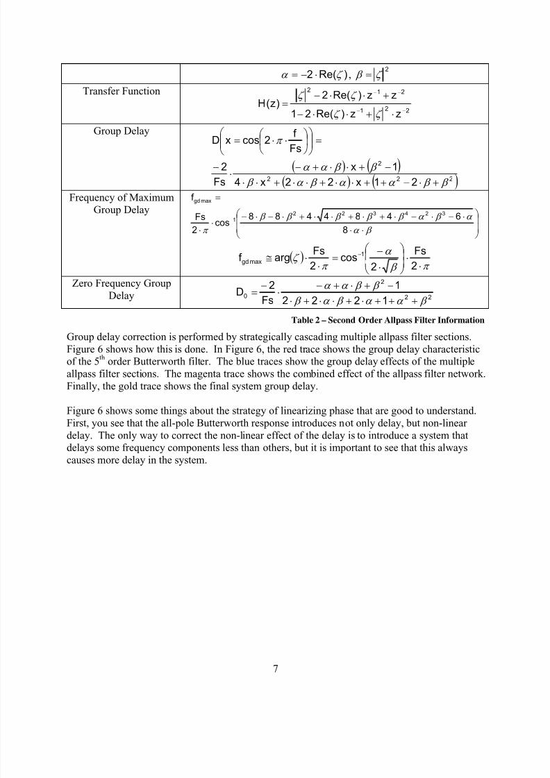
network. Table 1 and Table 2 outline some digital allpass filter characteristics.
Table 1 – First Order Allpass Filter Information
Transfer Function
1
1
1)(
−
−
⋅−
+−=
z
zzH
ζ
ζ
Group Delay
xFsFs
f xD
⋅⋅−+
−⋅=⎟⎟
⎠
⎞⎜⎜⎝
⎛ ⎟ ⎠
⎞⎜⎝
⎛ ⋅⋅=
ζ ζ
ζ π
21
112cos
2
2
Frequency of Maximum Group Delay 0max =gdf
Zero Frequency Group Delay(and Maximum Group Delay) ζ ζ
ζ
⋅−+
−⋅=
21
112
2
0Fs
D
8/9/2019 Group Delay Designcon2006
http://slidepdf.com/reader/full/group-delay-designcon2006 9/23
7
)Re(2 ζ α ⋅−= ,2
ζ β =
Transfer Function
221
212
)Re(21
)Re(2)(
−−
−−
⋅+⋅⋅−
+⋅⋅−=
zz
zzzH
ζ ζ
ζ ζ
Group Delay
( ) ( )( ) ( )222
2
21224
12
2cos
β β α α β α β
β β α α
π
+⋅−++⋅⋅+⋅⋅+⋅⋅
−+⋅⋅+−⋅
−
=⎟⎟ ⎠ ⎞⎜⎜
⎝ ⎛ ⎟
⎠ ⎞⎜
⎝ ⎛ ⋅⋅=
xx
x
Fs
Fsf xD
Frequency of MaximumGroup Delay
⎟⎟
⎠
⎞
⎜⎜
⎝
⎛
⋅⋅
⋅−⋅−⋅+⋅+⋅⋅+⋅−⋅−⋅
⋅
=
−
β α
α β α β β β β β
π 8
6484488cos
2
3243221
max
Fs
f gd
( )π
β
α
π ζ
⋅⋅
⎟⎟
⎠
⎞
⎜⎜
⎝
⎛
⋅
−=
⋅⋅≅ −
22
cos2
arg 1
max
FsFsf gd
Zero Frequency Group
Delay 22
2
01222
12
β α α β α β
β β α α
+++⋅+⋅⋅+⋅
−+⋅+−⋅
−=Fs
D
Table 2 – Second Order Allpass Filter Information
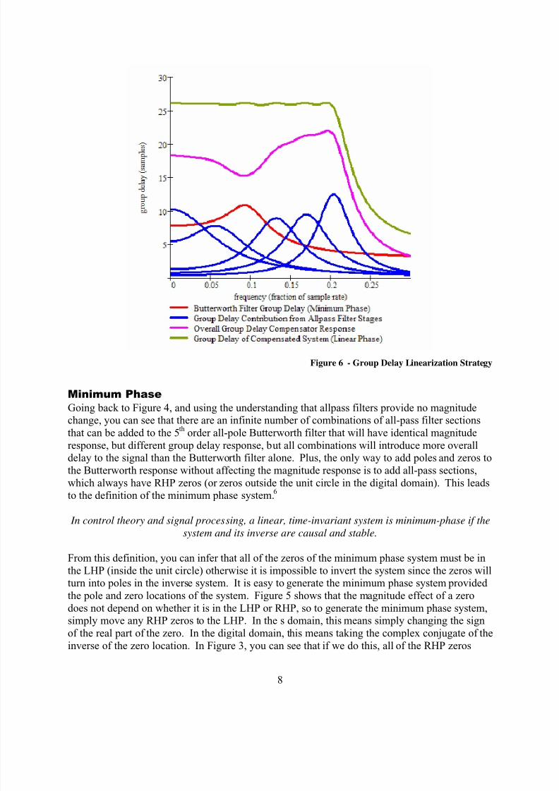
Group delay correction is performed by strategically cascading multiple allpass filter sections.
Figure 6 shows how this is done. In Figure 6, the red trace shows the group delay characteristicof the 5
th order Butterworth filter. The blue traces show the group delay effects of the multiple
allpass filter sections. The magenta trace shows the combined effect of the allpass filter network.
Finally, the gold trace shows the final system group delay.
Figure 6 shows some things about the strategy of linearizing phase that are good to understand.First, you see that the all-pole Butterworth response introduces not only delay, but non-linear
delay. The only way to correct the non-linear effect of the delay is to introduce a system thatdelays some frequency components less than others, but it is important to see that this always
causes more delay in the system.
8/9/2019 Group Delay Designcon2006
http://slidepdf.com/reader/full/group-delay-designcon2006 10/23
8
Figure 6 - Group Delay Linearization Strategy
Minimum Phase
Going back to Figure 4, and using the understanding that allpass filters provide no magnitudechange, you can see that there are an infinite number of combinations of all-pass filter sections
that can be added to the 5th
order all-pole Butterworth filter that will have identical magnitude
response, but different group delay response, but all combinations will introduce more overalldelay to the signal than the Butterworth filter alone. Plus, the only way to add poles and zeros to
the Butterworth response without affecting the magnitude response is to add all-pass sections,
which always have RHP zeros (or zeros outside the unit circle in the digital domain). This leadsto the definition of the minimum phase system.
6
In control theory and signal processing, a linear, time-invariant system is minimum-phase if the
system and its inverse are causal and stable.
From this definition, you can infer that all of the zeros of the minimum phase system must be inthe LHP (inside the unit circle) otherwise it is impossible to invert the system since the zeros willturn into poles in the inverse system. It is easy to generate the minimum phase system provided
the pole and zero locations of the system. Figure 5 shows that the magnitude effect of a zero
does not depend on whether it is in the LHP or RHP, so to generate the minimum phase system,simply move any RHP zeros to the LHP. In the s domain, this means simply changing the sign
of the real part of the zero. In the digital domain, this means taking the complex conjugate of the
inverse of the zero location. In Figure 3, you can see that if we do this, all of the RHP zeros
8/9/2019 Group Delay Designcon2006
http://slidepdf.com/reader/full/group-delay-designcon2006 11/23
9
would land on top of the added poles for phase compensation, and the minimum phase system is
simply the original 5th
order Butterworth filter.
This works for all-zero systems as well. If we have the impulse response of a system, we have
the filter coefficients of a FIR filter that defines the system:
N
N zazazaazH −−− ⋅++⋅+⋅+= ...)( 2
2
1
10 orN
N
NNN
z
azazazazH
++⋅+⋅+⋅=
−− ...)(
2
2
1
10
Equation 3 – Polynomial Representation of the Impulse Response
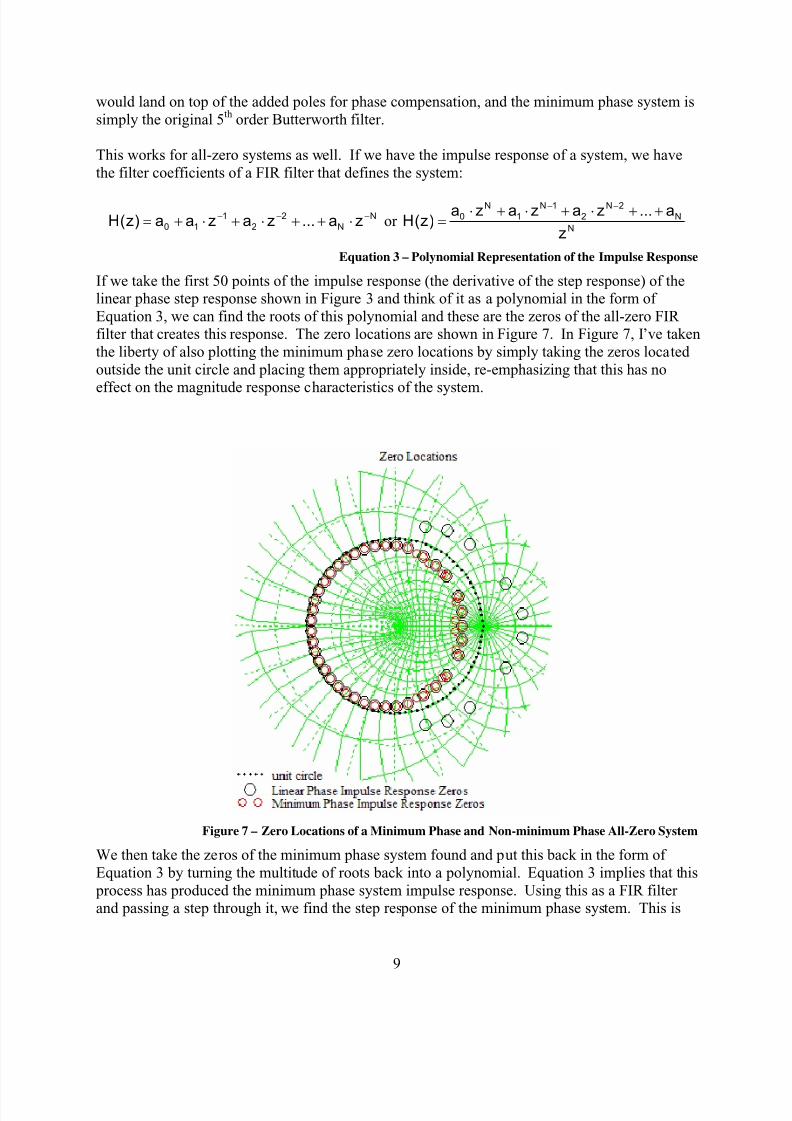
If we take the first 50 points of the impulse response (the derivative of the step response) of thelinear phase step response shown in Figure 3 and think of it as a polynomial in the form of
Equation 3, we can find the roots of this polynomial and these are the zeros of the all-zero FIRfilter that creates this response. The zero locations are shown in Figure 7. In Figure 7, I’ve taken
the liberty of also plotting the minimum phase zero locations by simply taking the zeros located
outside the unit circle and placing them appropriately inside, re-emphasizing that this has no
effect on the magnitude response characteristics of the system.
Figure 7 – Zero Locations of a Minimum Phase and Non-minimum Phase All-Zero System
We then take the zeros of the minimum phase system found and put this back in the form of
Equation 3 by turning the multitude of roots back into a polynomial. Equation 3 implies that this
process has produced the minimum phase system impulse response. Using this as a FIR filterand passing a step through it, we find the step response of the minimum phase system. This is
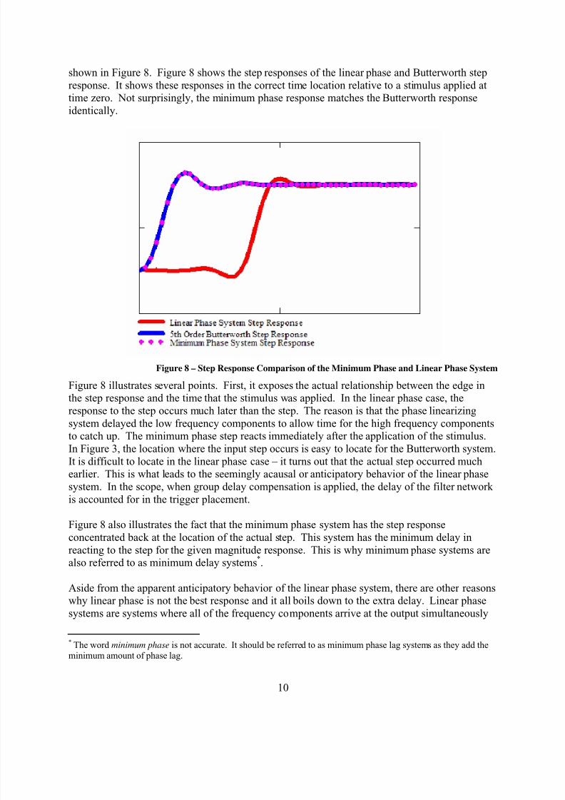
8/9/2019 Group Delay Designcon2006
http://slidepdf.com/reader/full/group-delay-designcon2006 12/23
10
shown in Figure 8. Figure 8 shows the step responses of the linear phase and Butterworth step
response. It shows these responses in the correct time location relative to a stimulus applied attime zero. Not surprisingly, the minimum phase response matches the Butterworth response
identically.
Figure 8 – Step Response Comparison of the Minimum Phase and Linear Phase System
Figure 8 illustrates several points. First, it exposes the actual relationship between the edge inthe step response and the time that the stimulus was applied. In the linear phase case, the
response to the step occurs much later than the step. The reason is that the phase linearizing
system delayed the low frequency components to allow time for the high frequency componentsto catch up. The minimum phase step reacts immediately after the application of the stimulus.
In Figure 3, the location where the input step occurs is easy to locate for the Butterworth system.
It is difficult to locate in the linear phase case – it turns out that the actual step occurred muchearlier. This is what leads to the seemingly acausal or anticipatory behavior of the linear phase
system. In the scope, when group delay compensation is applied, the delay of the filter network
is accounted for in the trigger placement.
Figure 8 also illustrates the fact that the minimum phase system has the step response
concentrated back at the location of the actual step. This system has the minimum delay in
reacting to the step for the given magnitude response. This is why minimum phase systems are
also referred to as minimum delay systems*.
Aside from the apparent anticipatory behavior of the linear phase system, there are other reasonswhy linear phase is not the best response and it all boils down to the extra delay. Linear phase
systems are systems where all of the frequency components arrive at the output simultaneously
* The word minimum phase is not accurate. It should be referred to as minimum phase lag systems as they add the
minimum amount of phase lag.
8/9/2019 Group Delay Designcon2006
http://slidepdf.com/reader/full/group-delay-designcon2006 13/23
11
but with additional delay. The simultaneity of the components is desirable from a distortion
standpoint and is clearly desirable in an audio system where the added delay is unimportant. Incommunications systems the added delay may or may not be important. In control systems,
however, the added delay is deadly and the minimum phase system is clearly desirable from a
controllability aspect.
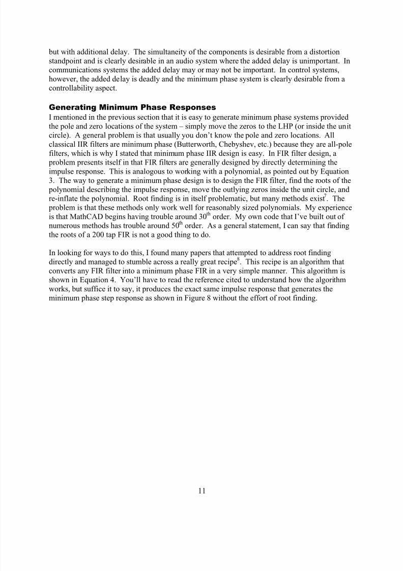
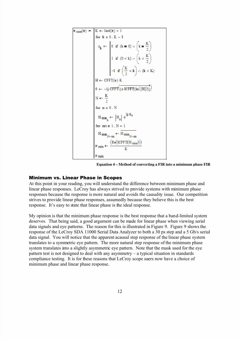
Generating Minimum Phase Responses
I mentioned in the previous section that it is easy to generate minimum phase systems provided
the pole and zero locations of the system – simply move the zeros to the LHP (or inside the unitcircle). A general problem is that usually you don’t know the pole and zero locations. All
classical IIR filters are minimum phase (Butterworth, Chebyshev, etc.) because they are all-pole
filters, which is why I stated that minimum phase IIR design is easy. In FIR filter design, a problem presents itself in that FIR filters are generally designed by directly determining the
impulse response. This is analogous to working with a polynomial, as pointed out by Equation
3. The way to generate a minimum phase design is to design the FIR filter, find the roots of the
polynomial describing the impulse response, move the outlying zeros inside the unit circle, and
re-inflate the polynomial. Root finding is in itself problematic, but many methods exist7
. The problem is that these methods only work well for reasonably sized polynomials. My experience
is that MathCAD begins having trouble around 30th
order. My own code that I’ve built out ofnumerous methods has trouble around 50
th order. As a general statement, I can say that finding
the roots of a 200 tap FIR is not a good thing to do.
In looking for ways to do this, I found many papers that attempted to address root finding
directly and managed to stumble across a really great recipe8. This recipe is an algorithm that
converts any FIR filter into a minimum phase FIR in a very simple manner. This algorithm isshown in Equation 4. You’ll have to read the reference cited to understand how the algorithm
works, but suffice it to say, it produces the exact same impulse response that generates the
minimum phase step response as shown in Figure 8 without the effort of root finding.
8/9/2019 Group Delay Designcon2006
http://slidepdf.com/reader/full/group-delay-designcon2006 14/23
12
Equation 4 – Method of converting a FIR into a minimum phase FIR
Minimum vs. Linear Phase in ScopesAt this point in your reading, you will understand the difference between minimum phase and
linear phase responses. LeCroy has always strived to provide systems with minimum phase
responses because the response is more natural and avoids the causality issue. Our competitionstrives to provide linear phase responses, assumedly because they believe this is the best
response. It’s easy to state that linear phase is the ideal response.
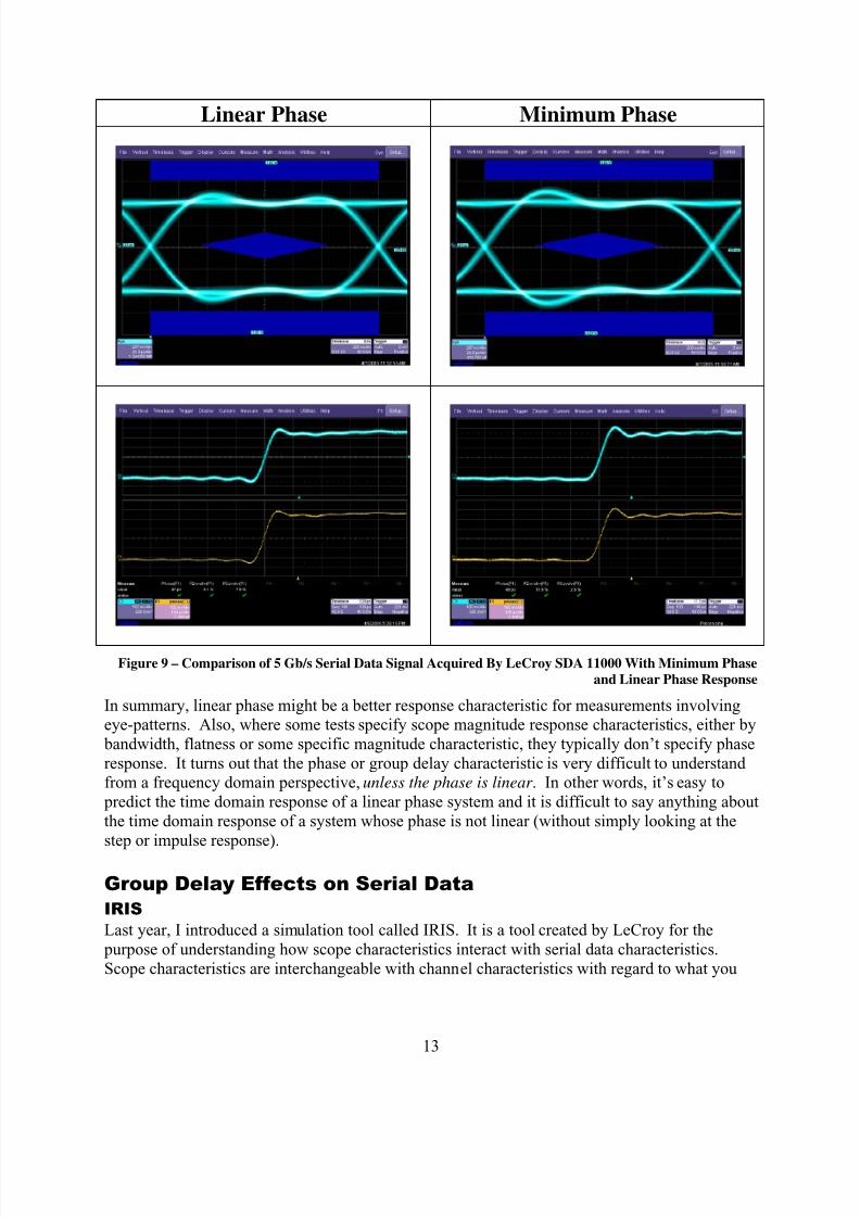
My opinion is that the minimum phase response is the best response that a band-limited system
deserves. That being said, a good argument can be made for linear phase when viewing serial
data signals and eye patterns. The reason for this is illustrated in Figure 9. Figure 9 shows theresponse of the LeCroy SDA 11000 Serial Data Analyzer to both a 30 ps step and a 5 Gb/s serial
data signal. You will notice that the apparent acausal step response of the linear phase systemtranslates to a symmetric eye pattern. The more natural step response of the minimum phase
system translates into a slightly asymmetric eye pattern. Note that the mask used for the eye pattern test is not designed to deal with any asymmetry – a typical situation in standards
compliance testing. It is for these reasons that LeCroy scope users now have a choice of
minimum phase and linear phase response.
8/9/2019 Group Delay Designcon2006
http://slidepdf.com/reader/full/group-delay-designcon2006 15/23
13
Linear Phase Minimum Phase
Figure 9 – Comparison of 5 Gb/s Serial Data Signal Acquired By LeCroy SDA 11000 With Minimum Phase
and Linear Phase Response
In summary, linear phase might be a better response characteristic for measurements involvingeye-patterns. Also, where some tests specify scope magnitude response characteristics, either by
bandwidth, flatness or some specific magnitude characteristic, they typically don’t specify phase
response. It turns out that the phase or group delay characteristic is very difficult to understandfrom a frequency domain perspective, unless the phase is linear . In other words, it’s easy to
predict the time domain response of a linear phase system and it is difficult to say anything about
the time domain response of a system whose phase is not linear (without simply looking at the
step or impulse response).
Group Delay Effects on Serial Data
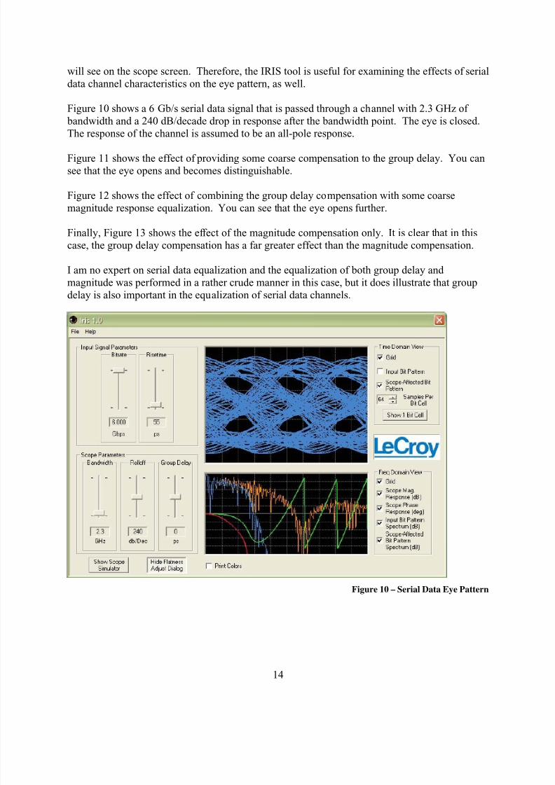
IRIS
Last year, I introduced a simulation tool called IRIS. It is a tool created by LeCroy for the
purpose of understanding how scope characteristics interact with serial data characteristics.
Scope characteristics are interchangeable with channel characteristics with regard to what you
8/9/2019 Group Delay Designcon2006
http://slidepdf.com/reader/full/group-delay-designcon2006 16/23
14
will see on the scope screen. Therefore, the IRIS tool is useful for examining the effects of serial
data channel characteristics on the eye pattern, as well.
Figure 10 shows a 6 Gb/s serial data signal that is passed through a channel with 2.3 GHz of
bandwidth and a 240 dB/decade drop in response after the bandwidth point. The eye is closed.
The response of the channel is assumed to be an all-pole response.
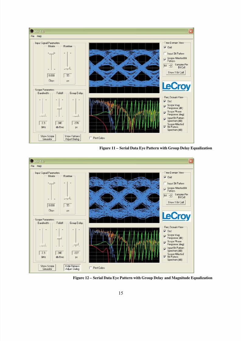
Figure 11 shows the effect of providing some coarse compensation to the group delay. You can
see that the eye opens and becomes distinguishable.
Figure 12 shows the effect of combining the group delay compensation with some coarse
magnitude response equalization. You can see that the eye opens further.
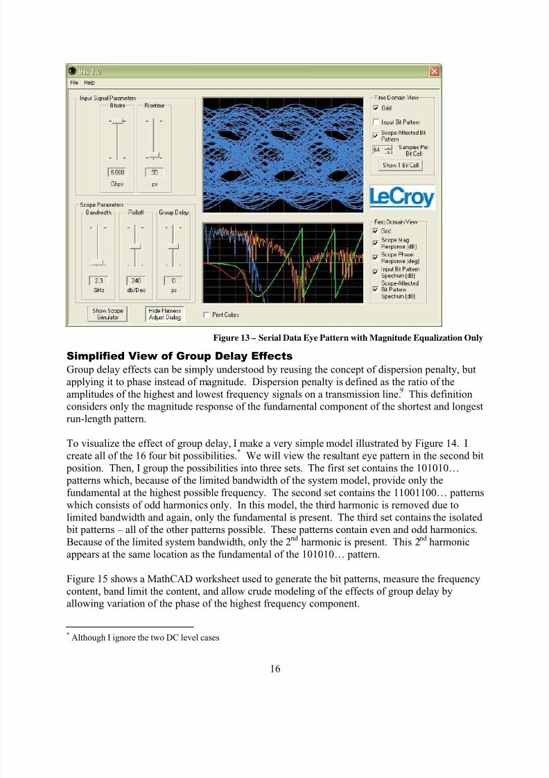
Finally, Figure 13 shows the effect of the magnitude compensation only. It is clear that in this
case, the group delay compensation has a far greater effect than the magnitude compensation.
I am no expert on serial data equalization and the equalization of both group delay andmagnitude was performed in a rather crude manner in this case, but it does illustrate that group
delay is also important in the equalization of serial data channels.
Figure 10 – Serial Data Eye Pattern
8/9/2019 Group Delay Designcon2006
http://slidepdf.com/reader/full/group-delay-designcon2006 17/23
15
Figure 11 – Serial Data Eye Pattern with Group Delay Equalization
Figure 12 – Serial Data Eye Pattern with Group Delay and Magnitude Equalization
8/9/2019 Group Delay Designcon2006
http://slidepdf.com/reader/full/group-delay-designcon2006 18/23
16
Figure 13 – Serial Data Eye Pattern with Magnitude Equalization Only
Simplified View of Group Delay Effects
Group delay effects can be simply understood by reusing the concept of dispersion penalty, but
applying it to phase instead of magnitude. Dispersion penalty is defined as the ratio of the
amplitudes of the highest and lowest frequency signals on a transmission line.9 This definition
considers only the magnitude response of the fundamental component of the shortest and longestrun-length pattern.
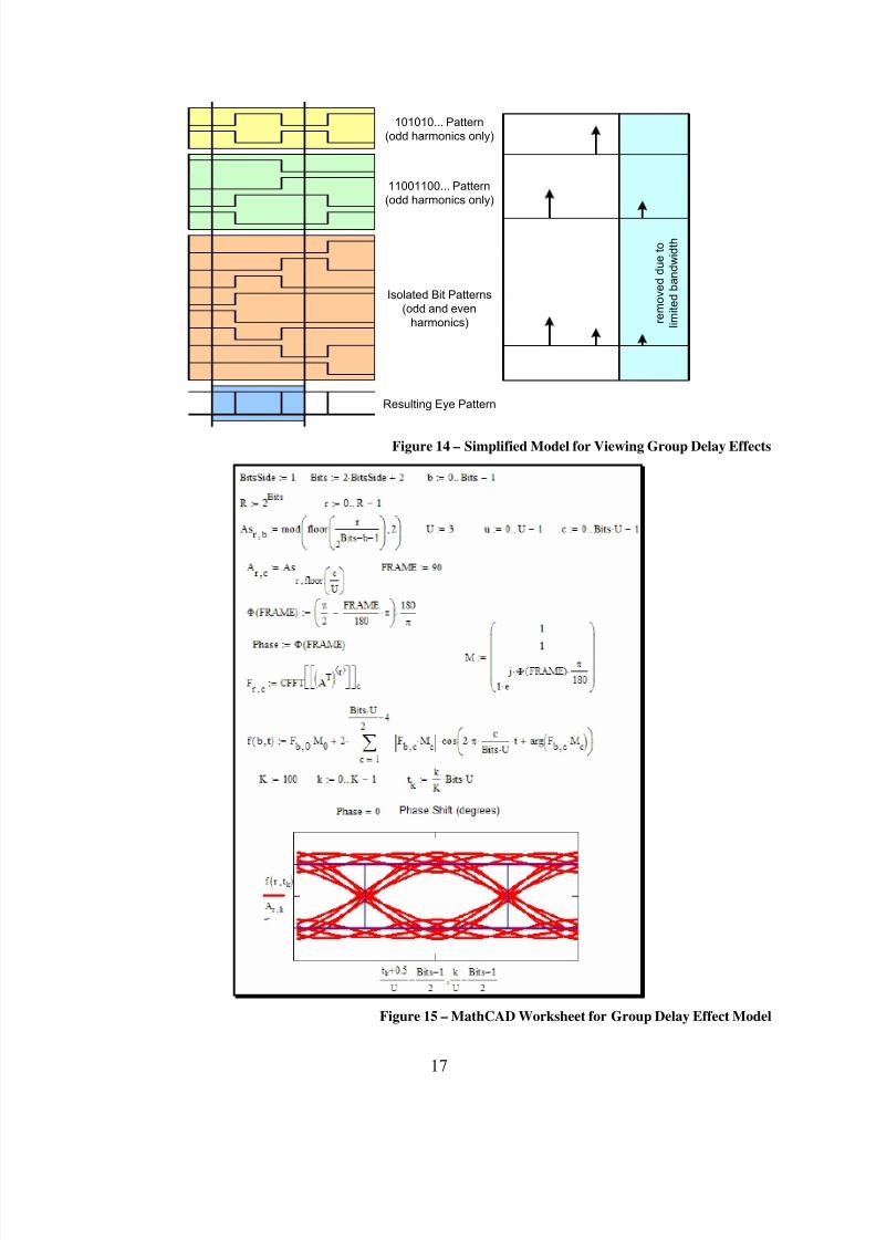
To visualize the effect of group delay, I make a very simple model illustrated by Figure 14. I
create all of the 16 four bit possibilities.* We will view the resultant eye pattern in the second bit
position. Then, I group the possibilities into three sets. The first set contains the 101010… patterns which, because of the limited bandwidth of the system model, provide only the
fundamental at the highest possible frequency. The second set contains the 11001100… patterns
which consists of odd harmonics only. In this model, the third harmonic is removed due to
limited bandwidth and again, only the fundamental is present. The third set contains the isolated bit patterns – all of the other patterns possible. These patterns contain even and odd harmonics.
Because of the limited system bandwidth, only the 2
nd
harmonic is present. This 2
nd
harmonicappears at the same location as the fundamental of the 101010… pattern.
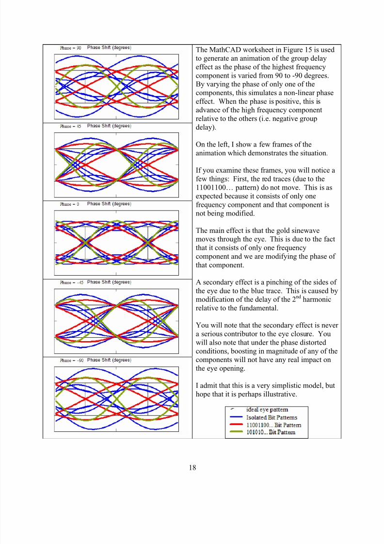
Figure 15 shows a MathCAD worksheet used to generate the bit patterns, measure the frequency
content, band limit the content, and allow crude modeling of the effects of group delay byallowing variation of the phase of the highest frequency component.
* Although I ignore the two DC level cases
8/9/2019 Group Delay Designcon2006
http://slidepdf.com/reader/full/group-delay-designcon2006 19/23
17
101010... Pattern
(odd harmonics only)
11001100... Pattern
(odd harmonics only)
Isolated Bit Patterns
(odd and even
harmonics) r e m o v e d d u e t o
l i m i t e d b a n d w i d t h
Resulting Eye Pattern
Figure 14 – Simplified Model for Viewing Group Delay Effects
Figure 15 – MathCAD Worksheet for Group Delay Effect Model
8/9/2019 Group Delay Designcon2006
http://slidepdf.com/reader/full/group-delay-designcon2006 20/23
18
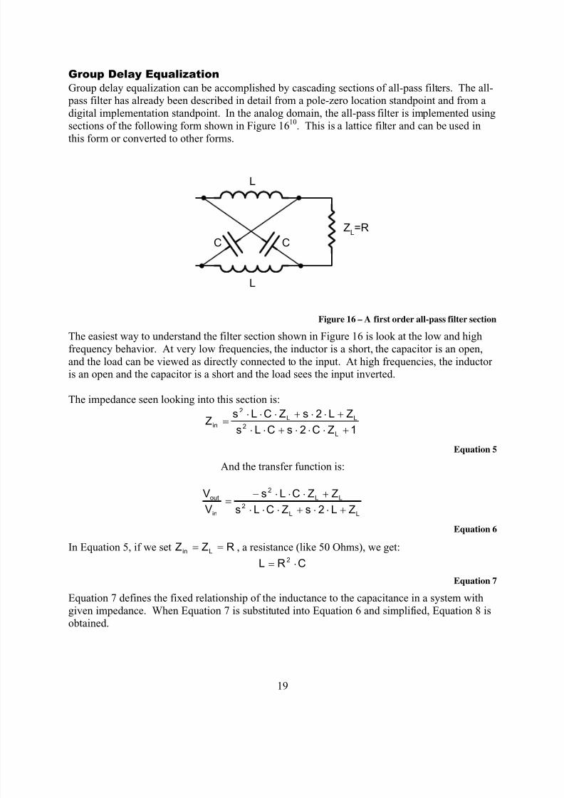
The MathCAD worksheet in Figure 15 is usedto generate an animation of the group delay
effect as the phase of the highest frequency
component is varied from 90 to -90 degrees.By varying the phase of only one of the
components, this simulates a non-linear phaseeffect. When the phase is positive, this isadvance of the high frequency component
relative to the others (i.e. negative group
delay).
On the left, I show a few frames of the
animation which demonstrates the situation.
If you examine these frames, you will notice a
few things: First, the red traces (due to the
11001100… pattern) do not move. This is asexpected because it consists of only one
frequency component and that component is
not being modified.
The main effect is that the gold sinewavemoves through the eye. This is due to the fact
that it consists of only one frequency
component and we are modifying the phase of
that component.
A secondary effect is a pinching of the sides ofthe eye due to the blue trace. This is caused bymodification of the delay of the 2
nd harmonic
relative to the fundamental.
You will note that the secondary effect is never
a serious contributor to the eye closure. You
will also note that under the phase distorted
conditions, boosting in magnitude of any of thecomponents will not have any real impact on
the eye opening.
I admit that this is a very simplistic model, but
hope that it is perhaps illustrative.
8/9/2019 Group Delay Designcon2006
http://slidepdf.com/reader/full/group-delay-designcon2006 21/23
19
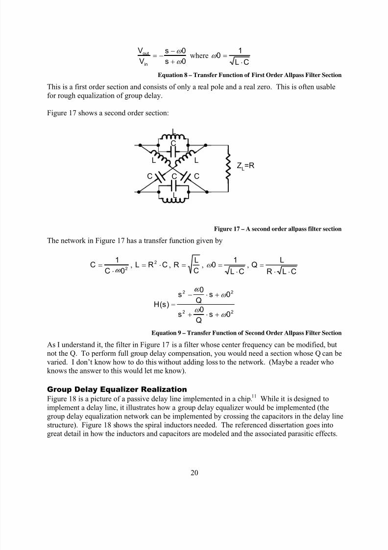
Group Delay Equalization
Group delay equalization can be accomplished by cascading sections of all-pass filters. The all- pass filter has already been described in detail from a pole-zero location standpoint and from a
digital implementation standpoint. In the analog domain, the all-pass filter is implemented using
sections of the following form shown in Figure 1610
. This is a lattice filter and can be used in
this form or converted to other forms.
CC
L
L
ZL=R
Figure 16 – A first order all-pass filter section
The easiest way to understand the filter section shown in Figure 16 is look at the low and high
frequency behavior. At very low frequencies, the inductor is a short, the capacitor is an open,
and the load can be viewed as directly connected to the input. At high frequencies, the inductoris an open and the capacitor is a short and the load sees the input inverted.
The impedance seen looking into this section is:
1222
2
+⋅⋅⋅+⋅⋅
+⋅⋅+⋅⋅⋅=
L
LLin
ZCsCLsZLsZCLsZ
Equation 5
And the transfer function is:
LL
LL
in
out
ZLsZCLs
ZZCLs
V
V
+⋅⋅+⋅⋅⋅
+⋅⋅⋅−=
22
2
Equation 6
In Equation 5, if we set RZZ Lin == , a resistance (like 50 Ohms), we get:
CRL ⋅= 2
Equation 7
Equation 7 defines the fixed relationship of the inductance to the capacitance in a system with
given impedance. When Equation 7 is substituted into Equation 6 and simplified, Equation 8 isobtained.
8/9/2019 Group Delay Designcon2006
http://slidepdf.com/reader/full/group-delay-designcon2006 22/23
20
0
0
ω
ω
+
−−=s
s
V
V
in
out whereCL ⋅
= 1
0ω
Equation 8 – Transfer Function of First Order Allpass Filter Section
This is a first order section and consists of only a real pole and a real zero. This is often usable
for rough equalization of group delay.
Figure 17 shows a second order section:
CC
L
L
C
C
LLZ
L=R
Figure 17 – A second order allpass filter section
The network in Figure 17 has a transfer function given by
20
1
⋅=C
C , CRL ⋅= 2,
C
LR = ,
CL ⋅=
10ω ,
CLR
LQ
⋅⋅=
22
22
00
00
)(
ω ω
ω
+⋅+
+⋅−
=
sQ
s
sQ
s
sH
Equation 9 – Transfer Function of Second Order Allpass Filter Section
As I understand it, the filter in Figure 17 is a filter whose center frequency can be modified, butnot the Q. To perform full group delay compensation, you would need a section whose Q can be
varied. I don’t know how to do this without adding loss to the network. (Maybe a reader whoknows the answer to this would let me know).
Group Delay Equalizer Realization
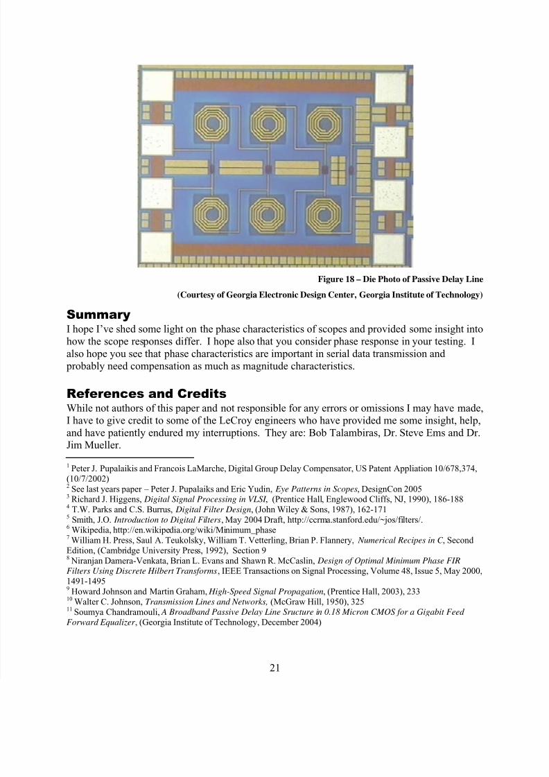
Figure 18 is a picture of a passive delay line implemented in a chip.11
While it is designed to
implement a delay line, it illustrates how a group delay equalizer would be implemented (the
group delay equalization network can be implemented by crossing the capacitors in the delay line
structure). Figure 18 shows the spiral inductors needed. The referenced dissertation goes intogreat detail in how the inductors and capacitors are modeled and the associated parasitic effects.
8/9/2019 Group Delay Designcon2006
http://slidepdf.com/reader/full/group-delay-designcon2006 23/23
Figure 18 – Die Photo of Passive Delay Line
(Courtesy of Georgia Electronic Design Center, Georgia Institute of Technology)
SummaryI hope I’ve shed some light on the phase characteristics of scopes and provided some insight into
how the scope responses differ. I hope also that you consider phase response in your testing. I
also hope you see that phase characteristics are important in serial data transmission and
probably need compensation as much as magnitude characteristics.
References and Credits
While not authors of this paper and not responsible for any errors or omissions I may have made,I have to give credit to some of the LeCroy engineers who have provided me some insight, help,
and have patiently endured my interruptions. They are: Bob Talambiras, Dr. Steve Ems and Dr.Jim Mueller.
1 Peter J. Pupalaikis and Francois LaMarche, Digital Group Delay Compensator, US Patent Appliation 10/678,374,
(10/7/2002)2 See last years paper – Peter J. Pupalaiks and Eric Yudin, Eye Patterns in Scopes, DesignCon 20053 Richard J. Higgens, Digital Signal Processing in VLSI , (Prentice Hall, Englewood Cliffs, NJ, 1990), 186-1884 T.W. Parks and C.S. Burrus, Digital Filter Design, (John Wiley & Sons, 1987), 162-1715 Smith, J.O. Introduction to Digital Filters, May 2004 Draft, http://ccrma.stanford.edu/~jos/filters/.6 Wikipedia, http://en.wikipedia.org/wiki/Minimum_phase7
William H. Press, Saul A. Teukolsky, William T. Vetterling, Brian P. Flannery, Numerical Recipes in C , SecondEdition, (Cambridge University Press, 1992), Section 98 Niranjan Damera-Venkata, Brian L. Evans and Shawn R. McCaslin, Design of Optimal Minimum Phase FIR
Filters Using Discrete Hilbert Transforms, IEEE Transactions on Signal Processing, Volume 48, Issue 5, May 2000,
1491-14959 Howard Johnson and Martin Graham, High-Speed Signal Propagation, (Prentice Hall, 2003), 23310 Walter C. Johnson, Transmission Lines and Networks, (McGraw Hill, 1950), 32511 Soumya Chandramouli, A Broadband Passive Delay Line Sructure in 0.18 Micron CMOS for a Gigabit Feed
Forward Equalizer , (Georgia Institute of Technology, December 2004)