Embed Size (px)
Citation preview

ZHANG ET AL. VOL. XXX ’ NO. XX ’ 000–000 ’ XXXX
www.acsnano.org
A
CXXXX American Chemical Society
Al-TiO2 Composite-ModifiedSingle-Layer Graphene as an EfficientTransparent Cathode for OrganicSolar CellsDi Zhang, Fengxian Xie, Peng Lin, and Wallace C. H. Choy*
Department of Electrical and Electronic Engineering, The University of Hong Kong, Pokfulam Road, Hong Kong
Graphene, which is a single sheetcomposed of hexagonally arrangedcarbon atoms, has attracted exten-
sive research interests.1 Of thewide range ofapplications deemed promising, a flexiblegraphene transparent electrode for organicsolar cells (OSCs) is quite attractive due to itsexcellent optical, electronic, and mechan-ical properties. One of the commonly uti-lized transparent electrodes in organic
optoelectronics is indium tin oxide (ITO),which is relatively expensive and chemicallyunstable.2,3 Moreover, ITO is rather brittle,4
which is not inherently compatible with theflexibility nature of organic materials. Beingonly one atom thick, graphene has uniformwhite light transmittance of over 97%,with a negligible reflectance of <0.1%.5 Ithas recently been reported that chemicallydoped large-area graphene can be readily
* Address correspondence [email protected].
Received for review December 18, 2012and accepted January 17, 2013.
Published online10.1021/nn3058399
ABSTRACT
While there are challenges in tuning the properties of graphene (surface wettability, work function alignment, and carrier transport) for realizing an
efficient graphene cathode in organic solar cells (OSCs), we propose and demonstrate using an Al-TiO2 composite to modify single-layer graphene as an
efficient cathode for OSCs. To unveil the contributions of the composite in addressing the aforementioned challenges, the evaporated aluminum
nanoclusters in the composite benefit the graphene cathode by simultaneously achieving two roles of improving its surface wettability for subsequent TiO2deposition and reducing its work function to offer better energy alignment. To address challenges related to charge transport, solution-processed TiO2 with
excellent electron transport can offer charge extraction enhancement to the graphene cathode, which is essential to efficient devices. However, it is a well-
known issue for methods such as spin-coating to produce uniform films on the initially hydrophobic graphene, even with improved wettability. The
undesirable morphology of TiO2 by such methods considerably inhibits its effectiveness in enhancing charge extraction. We propose a self-assembly method
to deposit the solution-processed TiO2 on the Al-covered graphene for forming the Al-TiO2 composite. Compared with spin-coating, the self-assembly
method is found to achieve more uniform coating on the graphene surface, with highly controllable thickness. Consequently, the graphene cathode
modified with the Al-TiO2 composite in inverted OSCs gives rise to enhanced power conversion efficiency of 2.58%, which is 2-fold of the previously best
reported efficiency (1.27%) for graphene cathode OSCs, reaching ∼75% performance of control devices using indium tin oxide.
KEYWORDS: organic solar cells . efficient graphene cathode . aluminumnanoclusters . titanium oxide . self-assembly film formation
ARTIC
LE

ZHANG ET AL. VOL. XXX ’ NO. XX ’ 000–000 ’ XXXX
www.acsnano.org
B
fabricated by a roll-to-roll method, with low sheetresistance (30Ω sq�1) comparable to that of ITO.6 Withthe advances in solution-processed fabrication ofchemically reduced graphene,7,8 it is promising thatlarge-area, high-quality graphene with low synthesiscosts will soon be available. Furthermore, it has beendemonstrated that the graphene electrode is moremechanically robust and flexible than ITO, showingsuperior performance under bending for flexible or-ganic optoelectronic devices such as organic light-emitting diodes9 and organic solar cells (OSCs).10,11
One of the key challenges is the interfacial modifica-tions for graphene electrodes. In addition to beingelectrically conductive and optically transparent, thework function (WF) of the electrodes should be tunedby interfacial modifications in accordance with themolecular orbital of the donor or the acceptor, in orderto minimize energy barriers at the anode or cathode,respectively. For graphene anodes, graphene oxide,12
poly(3,4-ethylenedioxythiophene):poly(styrenesulfonate)(PEDOT:PSS),11,13,14 and PEDOT/MoO3 double layers2
have been shown as effective hole transport layers(HTLs), with efficient power conversion efficiency (PCE)of 2.5�2.7% recorded. Previously, we have also re-ported PEDOT-free gold nanoclusters as an effectiveHTL for a multilayer graphene anode.15 Nevertheless,there is yet to be efficient OSCs using graphenecathodes. Jo et al. reported an inverted OSC using agraphene cathode modified by a polyfluorene inter-facial dipole layer, which yielded a PCE of 1.23%.16
Doped with alkali carbonate salt, a graphene/carbonnanotube cathode for inverted OSCs was reported byHuang et al., with 1.27% PCE.17 At present, the highestreported PCE for graphene cathode OSCs is still below1.3%.16�18 The realization of an efficient graphenecathode is crucial to the versatility and design flexibilityof graphene transparent electrodes.Meanwhile, inorganic transition metal oxides (p-type
and n-type) have newly emerged as promising candi-dates for fulfilling the role of efficient interface layers.19
Oxides such as MoO3, V2O5, and WO3 are good holetransportmaterials,20�23 whereas ones such as TiO2 andZnOaregoodelectron transportmaterials.24,25 Recently,efficient interface layers using solution-processedmetaloxides have been reported.23,25�27 However, for solu-tion processes, graphene electrodes need to overcomeits hydrophobic surface, which is initially not compatiblewith deposition methods such as spin-coating.28 There-fore, it is highly desirable to develop effective interfacialmodifications for a graphene cathode which can ad-dress its surfacewettability issuewhile enablingefficientOSC devices.In this work, we propose to introduce the composite
interface layer of aluminum (Al) nanoclusters andtitanium oxide (TiO2) to modify single-layer graphene(SLG) as a transparent cathode for inverted OSCs.Previously, WF lowering was observed on multilayer
graphene samples by using a subnanometer AlOx
layer.29 Differently, the Al-TiO2 composite in this worksimultaneously provides a series of interfacial modifi-cations on the graphene cathode, which enable effi-cient device operation of graphene cathode OSCs. Ascharacterized by contact angle measurement andultraviolet photoelectron spectroscopy (UPS), the thinAl nanoclusters in the Al-TiO2 composite significantlyimprove the surface wettability of SLG, while reducingits WF for better energy alignment and electron ex-traction. Furthermore, solution-processed TiO2 as anefficient electron transport material in the Al-TiO2
composite is essential to provide further charge extrac-tion enhancement on the Al-covered SLG. Its effective-ness for enhancing electron transport, however, may belimited by the poor uniformity of films deposited on thehydrophobic graphene. To address this well-known issuerelated to the graphene surface, we propose a self-assembly method which can readily deposit the subse-quent TiO2 solution on the Al-covered SLG. Compared tospin-coating, our self-assembly method can achievemore uniform and controllable coating of TiO2 films onthe initially hydrophobic SLG surface. As a result, the SLGcathodemodifiedwith the Al-TiO2 composite layer yieldsan efficient PCE of 2.58% in inverted OSCs, which ishigher than the previously reported efficiencies.
RESULTS AND DISCUSSION
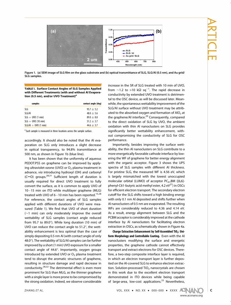
Al Nanoclusters on Graphene: Wettability Enhancementand Work Function Tuning. SLG films were transferred toa glass substrate assisted by poly(methylmethacrylate)(PMMA).30 Figure 1a is the scanning electron micro-scope (SEM) image of transferred SLG on the glasssubstrate. The SLG samples were characterized opticallyand electrically, with optical transmittance (Figure 1b,black line) of 96.0% at 500 nm and sheet resistance (SR)of ∼1.2 kΩ sq�1. The high and uniform transmittanceconfirms the graphene samples to be single layer.
Nevertheless, conformal coating of various solu-tion-processed interface layers on graphene remainsa challenging issue due to its intrinsically hydrophobicsurface. For solution-processed electron transport layers(ETLs) such as TiO2, we find that the solutions cannot bedirectly spin-coated on the SLG surface, which results inpoor device performance similar to that of device directlymade without ETL spin-coating (both cases PCE ∼ 0).
Here, we choose to improve the wettability of theSLG surface by thermally evaporating very thin Alnanoclusters as the first step of interfacial modifica-tions for the graphene cathode by the Al-TiO2 compo-site. For pristine SLG, the average contact angle islarge (95.7�, summarized in Table 1), suggesting a veryhydrophobic surface. Interestingly, when thin Al nano-clusters (∼0.5 nm) are evaporated onto SLG samples,the surface contact angle considerably reduces to48.0� (Table 1), indicating largely improved surfacewettability. Figure 2a,b illustrates the improvement
ARTIC
LE
ZHANG ET AL. VOL. XXX ’ NO. XX ’ 000–000 ’ XXXX
www.acsnano.org
C
accordingly. It should also be noted that the Al eva-poration on SLG only introduces a slight decreasein optical transparency, to 94.8% transmittance at500 nm, as shown in Figure 1b (blue line).
It has been shown that the uniformity of aqueousPEDOT:PSS on graphene can be improved by apply-ing ultraviolet-ozone (UVO) or O2 plasma treatment inadvance, via introducing hydroxyl (OH) and carbonyl(CdO) groups.28,31 Sufficient length of duration isusually required for direct UVO treatment to fullyconvert the surface, as it is common to apply UVO of10�15 min on ITO while multilayer graphene (MLG)treated with UVO of 6�10 min has been reported.15,28
For reference, the contact angles of SLG samplesapplied with different durations of UVO were mea-sured (Table 1). We find that UVO of short duration(∼1 min) can only moderately improve the overallwettability of SLG samples (contact angle reducedfrom 95.7 to 89.0�). While long duration (10 min) ofUVO can reduce the contact angle to 51.2�, the wett-ability enhancement is less optimal than the case ofsimply depositing 0.5 nmAl (with contact angle of only48.0�). The wettability of SLG/Al samples can be furtherimproved by a short (1min) UVO exposure for a smallercontact angle of 44.6�. Importantly, oxygen groupsintroduced by extended UVO or O2 plasma treatmenttend to disrupt the aromatic structures of graphene,resulting in structure damage and rapid decrease inconductivity.28,32 The detrimental effect is even moreprominent for SLG than MLG, as the thinner graphenewith a single layer ismore prone to be compromised bythe strong oxidation. Indeed, we observe considerable
increase in the SR of SLG treated with 10 min of UVO,from ∼1.2 to >10 kΩ sq�1. The rapid decrease inconductivity by extended UVO treatment is detrimen-tal to the OSC device, as will be discussed later. Mean-while, the spontaneouswettability improvement of theSLG/Al surface without UVO treatment may be attrib-uted to the absorbed oxygen and formation of AlOx atthe graphene/Al interface.29 Consequently, comparedto the direct oxidation of SLG by UVO, the ambientoxidation with thin Al nanoclusters on SLG providessignificantly better wettability enhancement, with-out compromising the conductivity of SLG for OSCperformance.
Importantly, besides improving the surface wett-ability, the thin Al nanoclusters on SLG contribute to amore energetically favorable cathode interface by low-ering the WF of graphene for better energy alignmentwith the organic acceptor. Figure 3 shows the UPSspectra of SLG samples with different Al thickness.For pristine SLG, the measured WF is 4.56 eV, whichis largely mismatched with the lowest unoccupiedmolecular orbital (LUMO) of acceptor PC61BM ([6,6]-phenyl-C61-butyric acid methyl ester, 4.2 eV27) in OSCsfor efficient electron transport. The secondary electroncutoff for the SLG shifts toward a high binding energywith only 0.1 nm Al deposited and shifts further whenAl nanoclusters of 0.5 nm are evaporated. The resultingWFs are considerably reduced to 4.36 and 4.14 eV.As a result, energy alignment between SLG and thePCBMacceptor is considerably improved at the cathodeinterface by Al nanoclusters for facilitating electronextraction in OSCs, as schematically shown in Figure 4a.
Charge Extraction Enhancement by Self-Assembled TiO2: Uni-form Morphology and Controllable Coating. Even with the Alnanoclusters modifying the surface and energeticproperties, the graphene cathode cannot effectivelytransport and extract electrons for OSC devices. There-fore, a two-step composite interface layer is required,in which an electron transport layer is further depos-ited on the Al-covered SLG to enhance electron extrac-tion. Solution-processed TiO2 nanocrystals are chosenin this work due to the excellent electron transportdemonstrated in ITO devices while being capableof large-area, low-cost applications.33 Nevertheless,
Figure 1. (a) SEM image of SLG film on the glass substrate and (b) optical transmittance of SLG, SLG/Al (0.5 nm), and Au grid/SLG samples.
TABLE 1. Surface Contact Angles of SLG Samples Applied
with Different Treatments (with and without Al Evapora-
tion (0.5 nm), and/or UVO Treatment)a
samples contact angle (deg)
SLG 95.7 ( 5.2SLG/Al 48.0 ( 5.6SLG þ UVO (1 min) 89.0 ( 8.8SLG þ UVO (10 min) 51.2 ( 3.7SLG/Al þ UVO (1 min) 44.6 ( 3.7
a Each sample is measured in three locations across the sample surface.
ARTIC
LE

ZHANG ET AL. VOL. XXX ’ NO. XX ’ 000–000 ’ XXXX
www.acsnano.org
D
depositing conformal and uniform films from solutionson the initially hydrophobic graphene surface is a well-known challenging issue, which may severely affectdevice performances. Indeed, we find that, usingconventional spin-coating, TiO2 films deposited onAl-covered SLG exhibit defective surface morphology,which results in rather poor performances for OSCdevices, as will be discussed later.
Here, we introduce a self-assembly method to fur-ther deposit solution-processed TiO2 on the Al-coveredSLG, in order to achieve uniform coating and enableefficient device performance. The TiO2 nanocrystals arestrategically dispersed in ethanol solution due to itsrelatively low surface tension and viscosity, indicatingthat the solution can form good contact with the elec-trode and spread uniformly. The weak intermolecularinteractions;hydrogen bond in ethanol;are respon-sible for nanoparticles aligning and arranging orderly.
In order to facilitate TiO2 nanocrystal alignment, wequickly cover the SLG/Al substrate by a small Petri dishafter casting the TiO2 solution onto the substrate. Theethanol solution then gradually spreads to cover theSLG surface. The evaporation rate of the solvent iscontrolled within the containment, while the wholeprocess takes about 30 min. It is worth noting thatthe evaporated Al is an important prerequisite for theself-assembly process, as we find that the TiO2 solutioncannot spread on the SLG surface with otherwise poorwettability as discussed in the previous section.
As a result, using the self-assembly method, TiO2
films with good uniformity and highly controllablethickness can be readily deposited on the SLG/Al sur-face, which is essential for effective charge extractionenhancement and efficient device performance. Ex-amined by SEM, we compare the surface morphologyof TiO2 films coated on the SLG/Al surface by spin-coating and self-assembly methods using identicalTiO2 solutions, as shown in Figure 5. We find thatdefect sites such as TiO2 aggregations are typical ofspin-coated films on SLG/Al, which are likely associatedwith the rapid solvent evaporation process not allow-ing gradual nanocrystal alignment (Figure 5a). Suchundesired aggregations are much fewer on TiO2 filmsdeposited by the self-assembly method, which yieldsmore uniform coating of the films (Figure 5b). Further-more, TiO2 films coated by the self-assembly processare also highly controllable, with thickness rangingfrom ∼10 to over 100 nm, readily obtained by varyingTiO2 concentration and solution casting volume. Incomparison, controllable thickness of TiO2 film onSLG/Al is difficult for the conventional method ofspin-coating. Our results show that spin-coated TiO2
film on SLG is rather thin with limited thickness (usually<20 nm regardless of spin-coating settings), even withthe improvedwettability byAl nanoclusters. Figure 6 showsa thickness comparisonmeasuredby cross-section SEMbe-tween spin-coatedandself-assembledTiO2filmsonSLG/Almade from TiO2 solution of the same concentration. Whileself-assembled TiO2 film coated on SLG/Al is quite thick(∼67.5 nm, 20μL solution-casted), spin-coatedTiO2filmonthe same substrate using identical solution is still very thin(∼19.0 nm, 80 μL solution-casted), even for a rather slowspin speed (1000 rpm). While multiple spin-coating pro-cesses may increase the coating thickness, the procedureis not easily controlled and the thickness only moderatelyincreases (see Figure S1 in Supporting Information), not tomention the surfacemorphologyof thefilmwhichmaybecompromised by the repeated process.
Device Performance of OSCs Using the Graphene Cathode. Tobetter show the contributions of the composite-mod-ified cathode to the OSC device performances, the SLGcathode modified with the Al-TiO2 composite interfacelayer was incorporated into poly(3-hexylthiophene)
Figure 2. Surface contact angles of (a) SLG and (b) SLG/Al (∼0.5 nm) samples.
Figure 3. UPS spectra and calculatedWFs of SLG and SLG/Al(0.1 and 0.5 nm) samples.
ARTIC
LE

ZHANG ET AL. VOL. XXX ’ NO. XX ’ 000–000 ’ XXXX
www.acsnano.org
E
(P3HT):PC61BM inverted OSCs (device structureschematically shown in Figure 4b). The device perfor-mances of a representative set of inverted OSCs withthe device structure of glass/cathode/P3HT:PC61BM(220 nm)/MoO3 (14 nm)/Ag (100 nm) are shown inFigure 7 and summarized in Table 2. While the surfacewettability of SLG can be moderately improved byextended UVO for subsequent self-assembled TiO2
deposition, the conductivity of graphene compro-mised in the process results in poor device perfor-mances (PCE∼ 0 for 10 min UVO). Using evaporated Alnanoclusters and self-assembled TiO2 as the Al-TiO2
composite ETL for the SLG cathode, the optimized
inverted SLG/Al-TiO2 OSCs reach an average PCE of1.59%. The Al-TiO2 composite demonstrates its effec-tiveness as an ETL for the graphene cathode byexhibiting good open-circuit voltage (VOC) of 0.58 Vand short-circuit current density (JSC) of 7.85 mA/cm2.As previously stated, the evaporated Al nanoclustersconsiderably improve the surface wettability and re-duce theWFof SLG cathode, which benefit subsequentfilm deposition and energy alignment at the cathodeinterface, respectively. The thickness of Al nanoclustersis found to be critical to device performances (shown inTable S1 in Supporting Information), as thicker Alevaporation may introduce excessive insulating AlOx
Figure 4. (a) Flat-band energy diagram of organic solar cells using the graphene cathodemodified by the Al-TiO2 composite.The work function decrease from pristine graphene (denoted by black dashed line, 4.6 eV) to graphene/Al (denoted by redsolid line, 4.1 eV) is indicated by upward red arrows. (b) Device structure of inverted organic solar cells using the graphenecathode shown in (a).
Figure 5. Surface SEM images of TiO2 films coated on the SLG/Al surface by (a) spin-coating and (b) self-assembly method,using identical TiO2 solutions. The visible TiO2 aggregations on spin-coated film are marked by arrows.
Figure 6. Cross-section SEM images of TiO2 films coated on the SLG/Al surface by (a) spin-coating and (b) self-assemblymethod, using identical TiO2 solutions.
ARTIC
LE

ZHANG ET AL. VOL. XXX ’ NO. XX ’ 000–000 ’ XXXX
www.acsnano.org
F
at the cathode interface. The Al nanocluster evapora-tion is followedby TiO2 deposition by the self-assemblymethod, which can achieve uniform and controllablecoating for effective electron extraction enhancement.In comparison, OSCs made from spin-coated TiO2 onthe SLG/Al cathode generally showedpoor VOC (0.30 V),due to the defective surface morphology of TiO2 filmscoated on SLG, as observed by SEM (Figure 5a).
Because of the high SR of intrinsic SLG itself(1.2 kΩ sq�1), the OSC devices suffer from additionalseries resistance from the graphene cathode, whichsignificantly limits the fill factor (FF) of the device(35.0%). Several methods have been reported to de-crease the SR of pristine graphene films, such as dopingchemically by acids, by gold particles, or by metalnanowires.2,6,11,31,34,35 For further device optimization,we deposit metallic (Au) grids onto the glass substratesprior to SLG transfer, which act as the electrical backbonefor the SLG electrode.36 The Au grids are beneath SLGfilms and are not in direct contact with the cathodeinterface. The deposition of the Au grids is detailed in theExperimental Section. The grid/SLG electrode showslargely enhanced conductivity (SR = 20�30 Ω sq�1)
comparable to ITO (SR = 20 Ω sq�1), while remainingoptically transparent (90.7% transmittance at 500 nm,Figure 1b, red line). By using Au grids to substantiallyincrease the conductivity of SLG cathodes, we observe aremarkable increase in FF (from 35.0 to 50.1%) and JSC(from 7.85 to 8.55 mA/cm2). As a result, the average PCEfor inverted OSCs using the SLG/Al-TiO2 cathode isimproved significantly to an efficient 2.58%, with desir-able FF and VOC (0.60 V). Interestingly, the average PCE ofthe optimized SLG cathode OSCs reaches ∼75% ofcontrol devices using the ITO cathode and identical Al-TiO2 composite interface layer (average PCE = 3.45%).
It should be noted that, with the addition of Augrids underneath graphene, the thickness of the Augrids (50 nm) may introduce uneven morphology forthin TiO2 coating, which was optimized from grapheneOSCs without the grids. Therefore, a thicker TiO2 layer,which can offset the height difference between thegrid-covered and noncovered surface, is utilized toimprove morphology and optimize the performance.By increasing TiO2 thickness, we observed consider-ably improved performance in OSCs using Au grids(as shown in Table S2 in Supporting Information). In orderto confirm that Au grids merely function as conductivityenhancement for the SLG cathode, grid-only OSCs wereconstructed using Au grids as the intended cathodemodifiedwith an Al-TiO2 layer, without the SLG between.The grid-only OSCs exhibited very small JSC (1.31 mA/cm2) due to the large grid spacing and poor FF (33.2%),possibly due to the mismatchedWF of Au (∼5.2 eV). Theresulting PCE of 0.27% confirms the significance of theSLG cathode in the OSC devices.
CONCLUSIONS
In conclusion, we have proposed and demonstratedthe interface engineering of graphene as a transparentcathode for inverted OSCs by an Al-TiO2 compositeinterface layer. The thin Al nanoclusters in the Al-TiO2
composite simultaneously improve the surface wett-ability of SLG for subsequent TiO2 deposition andreduce its WF for better energy alignment. We intro-duce a self-assembly approach for TiO2 deposition andcareful selection of ethanol solvent to form TiO2 films onSLG with uniform surface morphology and highly con-trollable thickness. The two-step modifications form anoptimized Al-TiO2 composite interface layer for SLG tofunction as an effective cathode for OSC devices. As aresult, the transparent SLG cathodemodifiedwith the Al-TiO2 composite layer yields an optimized PCE of 2.58% ininverted OSCs, demonstrating more efficient perfor-mances than those of previously reported.
EXPERIMENTAL SECTIONMaterials. SLG films synthesized by a chemical vapor deposi-
tion (CVD) process37 on copper foils were purchased from
Graphene Supermarket. Copper foils were etched away byiron(III) chloride solution (20 mg/mL), while SLG films weresupported and transferred to glass substrates by PMMA.30
Figure 7. J�V characteristics of a representative set ofinverted PSCs with the device structure of cathode/P3HT:PC61BM (220 nm)/MoO3 (14 nm)/Ag (100 nm).
TABLE 2. Device Performance of a Representative Set
of Inverted PSCs with the Device Structure of Cathode/
P3HT:PC61BM (220 nm)/MoO3 (14 nm)/Ag (100 nm)
cathode structure JSC (mA/cm2) VOC (V) FF (%) PCE (%)
SLG/Al-TiO2 7.85 ( 0.24 0.58 ( 0.02 35.0 ( 3.2 1.59 ( 0.08grid/SLG/Al-TiO2 8.55 ( 0.62 0.60 ( 0.01 50.1 ( 2.5 2.58 ( 0.09ITO/Al-TiO2 9.11 ( 0.25 0.63 ( 0.00 60.1 ( 0.3 3.45 ( 0.09SLG/Al/spin-coated TiO2 1.80 ( 0.65 0.30 ( 0.04 25.2 ( 0.5 0.14 ( 0.07grid only/Al-TiO2 1.31 ( 0.56 0.61 ( 0.01 33.2 ( 0.5 0.27 ( 0.11SLG/TiO2 þ UVO (10 min) 0
ARTIC
LE
ZHANG ET AL. VOL. XXX ’ NO. XX ’ 000–000 ’ XXXX
www.acsnano.org
G
The ligand-free anatase TiO2 nanocrystals were synthesized bya non-aqueous method,38 with the TiO2 nanoparticles being∼4 nm in size and dispersed in ethanol.
Device Fabrication. Gold grids were thermally evaporatedonto the glass substrates prior to SLG transfer to enhance theconductivity of the SLG cathode, which are beneath SLG filmsand are not in direct contact with the cathode interface. The Augrids are 50 nm thick, with line width of 10 μm and grid spacingof 200 μm. Aluminum nanoclusters were thermally evaporatedonto SLG samples under 6� 10�4 Pa, with thickness monitoredby a quartz sensor. After Al evaporation, the SLG/Al sampleswere treated with short UVO (1 min). The Al-TiO2 compositelayer on SLG was finished by depositing solution-processedTiO2 nanocrystals using a self-assembly method.33 After theself-assembly/spin-coating process, all TiO2 films (30�40 nm)were annealed at 150 �C for 10 min on a hot plate in ambientconditions. The prepared SLG samples were then transferredinto a nitrogen-filled glovebox for spin-coating the blend ofpoly(3-hexylthiophene) (P3HT) and [6,6]-phenyl-C61-butyricacid methyl ester (PC61BM) with 1:1 weight ratio (20 mg/mLeach dissolved in 1,2-dichlorobenzene). Before annealing at130 �C for 10 min on a hot plate, solvent annealing is utilized asdescribed elsewhere.39 MoO3 (14 nm)/Ag (100 nm) was ther-mally evaporated as the top anode, which defines the devicearea as 0.04�0.06 cm2. The final device structure was SLG/Al-TiO2/P3HT:PC61BM (220 nm)/MoO3 (14 nm)/Ag (100 nm). Forreference, the ITO cathode using an identical Al-TiO2 compositeETL was incorporated in the OSC device with the structure ofITO/Al-TiO2/P3HT:PC61BM/MoO3/Ag.
Characterizations. Current density�voltage (J�V) characteris-tics were measured by using a Keithley 2635 sourcemeter andABET AM1.5G solar simulator. UPS measurement was carriedout by using a He discharged lamp (He I 21.22 eV, Kratos Anal-ytical). SEM images were obtained using a Hitachi S-4800 FEGscanning electron microscope.
Conflict of Interest: The authors declare no competingfinancial interest.
Acknowledgment. This work is supported by UniversityGrant Council of the University of Hong Kong (Grant Nos.10401466 and 201111159062), and the General Research Fund(Grants Nos. HKU712010E andHKU711612E), and the RGC-NSFCgrant (N_HKU709/12) from the Research Grants Council of HongKong Special Administrative Region, China. D.Z. would like toacknowledge Hong Kong Ph.D. Fellowship from the ResearchGrants Council of Hong Kong.We acknowledge the help of EricaChang and Tony Feng for measuring contact angle of oursamples, and Xuanhua Li for conducting SEM measurement.
Supporting Information Available: Thickness increment ofTiO2 layer spin-coated multiple times (Figure S1) and deviceperformance of inverted PSCs using SLG/Al-TiO2 cathode withdifferent Al thickness (Table S1) and different TiO2 thickness(Table S2). This material is available free of charge via theInternet at http://pubs.acs.org.
REFERENCES AND NOTES1. Novoselov, K.; Geim, A.; Morozov, S.; Jiang, D.; Zhang, Y.;
Dubonos, S.; Grigorieva, I.; Firsov, A. Electric Field Effect inAtomically Thin Carbon Films. Science 2004, 306, 666–669.
2. Wang, Y.; Tong, S. W.; Xu, X. F.; €Ozyilmaz, B.; Loh, K. P. Inter-face Engineering of Layer-by-Layer Stacked GrapheneAnodes for High-Performance Organic Solar Cells. Adv.Mater. 2011, 23, 1514–1518.
3. Schlatmann, A. Indium Contamination from the Indium-Tin-Oxide Electrode in Polymer Light-Emitting Diodes.Appl. Phys. Lett. 1996, 69, 1764.
4. Chen, Z.; Cotterell, B.; Wang, W.; Guenther, E.; Chua, S.-J.A Mechanical Assessment of Flexible OptoelectronicDevices. Thin Solid Films 2001, 394, 201–205.
5. Nair, R.; Blake, P.; Grigorenko, A.; Novoselov, K.; Booth, T.;Stauber, T.; Peres, N.; Geim, A. Fine Structure ConstantDefines Visual Transparency of Graphene. Science 2008,320, 1308.
6. Bae, S.; Kim, H.; Lee, Y.; Xu, X.; Park, J.-S.; Zheng, Y.;Balakrishnan, J.; Lei, T.; Ri Kim, H.; Song, Y. I.; et al. Roll-to-Roll Production of 30-Inch Graphene Films for TransparentElectrodes. Nat. Nanotechnol. 2010, 5, 574–578.
7. Sire, C.; Ardiaca, F.; Lepilliet, S.; Seo, J.-W. T.; Hersam, M. C.;Dambrine, G.; Happy, H.; Derycke, V. Flexible GigahertzTransistors Derived from Solution-Based Single-Layer Gra-phene. Nano Lett. 2012, 12, 1184–1188.
8. Wöbkenberg, P. H.; Eda, G.; Leem, D. S.; de Mello, J. C.;Bradley, D. D. C.; Chhowalla, M.; Anthopoulos, T. D. Re-duced Graphene Oxide Electrodes for Large Area OrganicElectronics. Adv. Mater. 2011, 23, 1558–1562.
9. Han, T. H.; Lee, Y.; Choi, M. R.; Woo, S. H.; Bae, S. H.; Hong,B. H.; Ahn, J. H.; Lee, T. W. Extremely Efficient FlexibleOrganic Light-Emitting Diodes with Modified GrapheneAnode. Nat. Photonics 2012, 6, 105–110.
10. Gomez De Arco, L.; Zhang, Y.; Schlenker, C. W.; Ryu, K.;Thompson, M. E.; Zhou, C. Continuous, Highly Flexible, andTransparent Graphene Films by Chemical Vapor Deposi-tion for Organic Photovoltaics. ACS Nano 2010, 4, 2865–2873.
11. Lee, S.; Yeo, J. S.; Ji, Y.; Cho, C.; Kim, D. Y.; Na, S. I.; Lee, B. H.;Lee, T. Flexible Organic Solar Cells Composed of P3HT:PCBM Using Chemically Doped Graphene Electrodes.Nanotechnology 2012, 23, 344013.
12. Lee, Y.-Y.; Tu, K.-H.; Yu, C.-C.; Li, S.-S.; Hwang, J.-Y.; Lin, C.-C.;Chen, K.-H.; Chen, L.-C.; Chen, H.-L.; Chen, C.-W. TopLaminated Graphene Electrode in a Semitransparent Poly-mer Solar Cell by Simultaneous Thermal Annealing/Releasing Method. ACS Nano 2011, 5, 6564–6570.
13. Hsu, C. L.; Lin, C. T.; Huang, J. H.; Chu, C. W.; Wei, K. H.; Li, L. J.Layer-by-Layer Graphene/TCNQ Stacked Films as Con-ducting Anodes for Organic Solar Cells. ACS Nano 2012,6, 5031–5039.
14. Liu, Z.; Li, J.; Sun, Z.-H.; Tai, G.; Lau, S.-P.; Yan, F. TheApplication of Highly Doped Single-Layer Graphene asthe Top Electrodes of Semitransparent Organic Solar Cells.ACS Nano 2011, 6, 810–818.
15. Zhang, D.; Choy,W. C. H.; Wang, C. C. D.; Li, X.; Fan, L.; Wang,K.; Zhu, H. Polymer Solar Cells with Gold NanoclustersDecorated Multi-Layer Graphene as Transparent Elec-trode. Appl. Phys. Lett. 2011, 99, 223302.
16. Jo, G.; Na, S.-I.; Oh, S.-H.; Lee, S.; Kim, T.-S.; Wang, G.; Choe,M.; Park,W.; Yoon, J.; Kim, D.-Y.; et al. Tuning of aGraphene-Electrode Work Function To Enhance the Efficiency ofOrganic Bulk Heterojunction Photovoltaic Cells with anInverted Structure. Appl. Phys. Lett. 2010, 97, 213301.
17. Huang, J. H.; Fang, J. H.; Liu, C. C.; Chu, C. W. Effective WorkFunction Modulation of Graphene/Carbon NanotubeComposite Films as Transparent Cathodes for OrganicOptoelectronics. ACS Nano 2011, 5, 6262–6271.
18. Cox, M.; Gorodetsky, A.; Kim, B.; Kim, K. S.; Jia, Z.; Kim, P.;Nuckolls, C.; Kymissis, I. Single-Layer Graphene Cathodesfor Organic Photovoltaics. Appl. Phys. Lett. 2011, 98, 123303.
19. Greiner, M. T.; Helander, M. G.; Tang, W.-M.; Wang, Z.-B.;Qiu, J.; Lu, Z.-H. Universal Energy-Level Alignment ofMolecules on Metal Oxides. Nat. Mater. 2012, 11, 76–81.
20. Tao, C.; Ruan, S.; Zhang, X.; Xie, G.; Shen, L.; Kong, X.; Dong,W.; Liu, C.; Chen,W. Performance Improvement of InvertedPolymer Solar Cells withDifferent Top Electrodes by Introdu-cing a MoO3 Buffer Layer. Appl. Phys. Lett. 2008, 93, 193307.
21. Tao, C.; Ruan, S.; Xie, G.; Kong, X.; Shen, L.; Meng, F.; Liu, C.;Zhang, X.; Dong, W.; Chen, W. Role of Tungsten Oxide inInverted Polymer Solar Cells.Appl. Phys. Lett.2009, 94, 043311.
22. Huang, J.-S.; Chou, C.-Y.; Liu, M.-Y.; Tsai, K.-H.; Lin, W.-H.; Lin,C.-F. Solution-Processed Vanadium Oxide as an AnodeInterlayer for Inverted Polymer Solar Cells Hybridized withZnO Nanorods. Org. Electron. 2009, 10, 1060–1065.
23. Meyer, J.; Khalandovsky, R.; Görrn, P.; Kahn, A. MoO3 FilmsSpin-Coated from a Nanoparticle Suspension for EfficientHole-Injection in Organic Electronics. Adv. Mater. 2011, 23,70–73.
24. Park, M.-H.; Li, J.-H.; Kumar, A.; Li, G.; Yang, Y. Doping of theMetal Oxide Nanostructure and Its Influence in OrganicElectronics. Adv. Funct. Mater. 2009, 19, 1241–1246.
ARTIC
LE
ZHANG ET AL. VOL. XXX ’ NO. XX ’ 000–000 ’ XXXX
www.acsnano.org
H
25. Hau, S. K.; Yip, H.-L.; Baek, N. S.; Zou, J.; O'Malley, K.; Jen,A. K. Y. Air-Stable Inverted Flexible Polymer Solar CellsUsing Zinc Oxide Nanoparticles as an Electron SelectiveLayer. Appl. Phys. Lett. 2008, 92, 253301.
26. Lee, Y.-J.; Yi, J.; Gao, G. F.; Koerner, H.; Park, K.; Wang, J.; Luo,K.; Vaia, R. A.; Hsu, J. W. P. Low-Temperature Solution-Processed Molybdenum Oxide Nanoparticle Hole Trans-port Layers for Organic Photovoltaic Devices. Adv. EnergyMater. 2012, 2, 1193–1197.
27. You, J.; Chen, C.-C.; Dou, L.; Murase, S.; Duan, H.-S.; Hawks,S. A.; Xu, T.; Son, H. J.; Yu, L.; Li, G.; et al. Metal OxideNanoparticles as an Electron-Transport Layer in High-Performance and Stable Inverted Polymer Solar Cells.Adv. Mater. 2012, 24, 5267–5272.
28. Wang, Y.; Chen, X.; Zhong, Y.; Zhu, F.; Loh, K. P. Large Area,Continuous, Few-Layered Graphene as Anodes in OrganicPhotovoltaic Devices. Appl. Phys. Lett. 2009, 95, 063302.
29. Yi, Y.; Choi, W.M.; Kim, Y. H.;Won Kim, J.; Kang, S. J. EffectiveWork Function Lowering of Multilayer Graphene Films bySubnanometer Thick AlOx Overlayers. Appl. Phys. Lett.2011, 98, 013505.
30. Reina, A.; Son, H.; Jiao, L.; Fan, B.; Dresselhaus, M. S.; Liu, Z.;Kong, J. Transferring and Identification of Single- and Few-Layer Graphene on Arbitrary Substrates. J. Phys. Chem. C2008, 112, 17741–17744.
31. Hyesung, P.; Rowehl, J. A.; Kim, K. K.; Bulovic, V.; Kong, J.Doped Graphene Electrodes for Organic Solar Cells. Nano-technology 2010, 21, 505204.
32. Shin, Y. J.; Wang, Y.; Huang, H.; Kalon, G.; Wee, A. T. S.; Shen,Z.; Bhatia, C. S.; Yang, H. Surface-Energy Engineering ofGraphene. Langmuir 2010, 26, 3798–3802.
33. Zhang, D.; Choy, W. C. H.; Xie, F.-x.; Li, X. Large-Area, High-Quality Self-Assembly Electron Transport Layer for Organ-ic Optoelectronic Devices. Org. Electron. 2012, 13, 2042–2046.
34. Günes-, F.; Shin, H. J.; Biswas, C.; Han, G. H.; Kim, E. S.; Chae,S. J.; Choi, J. Y.; Lee, Y. H. Layer-by-Layer Doping of Few-Layer Graphene Film. ACS Nano 2010, 4, 4595.
35. Kholmanov, I. N.; Magnuson, C. W.; Aliev, A. E.; Li, H.; Zhang,B.; Suk, J. W.; Zhang, L. L.; Peng, E.; Mousavi, S. H.; Khanikaev,A. B.; et al. Improved Electrical Conductivity of GrapheneFilms Integrated with Metal Nanowires. Nano Lett. 2012, 12,5679–5683.
36. Zhu, Y.; Sun, Z.; Yan, Z.; Jin, Z.; Tour, J. M. Rational Design ofHybrid Graphene Films for High-Performance TransparentElectrodes. ACS Nano 2011, 5, 6472–6479.
37. Li, X.; Cai, W.; An, J.; Kim, S.; Nah, J.; Yang, D.; Piner, R.;Velamakanni, A.; Jung, I.; Tutuc, E.; et al. Large-Area Synthe-sis of High-Quality and Uniform Graphene Films onCopper Foils. Science 2009, 324, 1312–1314.
38. Jensen, G. V.; Bremholm, M.; Lock, N.; Deen, G. R.; Jensen,T. R.; Iversen, B. B.; Niederberger, M.; Pedersen, J. S.;Birkedal, H. Anisotropic Crystal Growth Kinetics of AnataseTiO2 Nanoparticles Synthesized in aNonaqueousMedium.Chem. Mater. 2010, 22, 6044–6055.
39. Li, G.; Shrotriya, V.; Huang, J.; Yao, Y.; Moriarty, T.; Emery, K.;Yang, Y. High-Efficiency Solution Processable PolymerPhotovoltaic Cells by Self-Organization of Polymer Blends.Nat. Mater. 2005, 4, 864–868.
ARTIC
LE