Embed Size (px)
Citation preview
Subscriber access provided by ECU Libraries
ACS Nano is published by the American Chemical Society. 1155 Sixteenth StreetN.W., Washington, DC 20036Published by American Chemical Society. Copyright © American Chemical Society.However, no copyright claim is made to original U.S. Government works, or worksproduced by employees of any Commonwealth realm Crown government in the courseof their duties.
Article
Archimedean Tilings and Hierarchical Lamellar MorphologyFormed by Semicrystalline Miktoarm Star Terpolymer Thin Films
Karim Aissou, Wonsang Kwon, muhammad mumtaz, Segolene Antoine,Mireille Maret, Giuseppe Portale, Guillaume Fleury, and Georges Hadziioannou
ACS Nano, Just Accepted Manuscript • DOI: 10.1021/acsnano.5b06728 • Publication Date (Web): 29 Mar 2016
Downloaded from http://pubs.acs.org on March 30, 2016
Just Accepted
“Just Accepted” manuscripts have been peer-reviewed and accepted for publication. They are postedonline prior to technical editing, formatting for publication and author proofing. The American ChemicalSociety provides “Just Accepted” as a free service to the research community to expedite thedissemination of scientific material as soon as possible after acceptance. “Just Accepted” manuscriptsappear in full in PDF format accompanied by an HTML abstract. “Just Accepted” manuscripts have beenfully peer reviewed, but should not be considered the official version of record. They are accessible to allreaders and citable by the Digital Object Identifier (DOI®). “Just Accepted” is an optional service offeredto authors. Therefore, the “Just Accepted” Web site may not include all articles that will be publishedin the journal. After a manuscript is technically edited and formatted, it will be removed from the “JustAccepted” Web site and published as an ASAP article. Note that technical editing may introduce minorchanges to the manuscript text and/or graphics which could affect content, and all legal disclaimersand ethical guidelines that apply to the journal pertain. ACS cannot be held responsible for errorsor consequences arising from the use of information contained in these “Just Accepted” manuscripts.
Archimedean Tilings and Hierarchical Lamellar Morphology Formed by
Semicrystalline Miktoarm Star Terpolymer Thin Films
Karim Aissou,1*# Wonsang Kwon,1# Muhammad Mumtaz,1,2 Ségolène Antoine,1 Mireille
Maret,3 Giuseppe Portale,4 Guillaume Fleury,1* and Georges Hadziioannou1
1Laboratoire de Chimie des Polymères Organiques, CNRS - ENSCPB - Université de Bordeaux, 16 Avenue Pey-Berland, F-33607 Pessac Cedex, France
2ARKEMA, Groupement de Recherches de Lacq, RN 117, BP 34, F-64170 Lacq Cedex, France 3 Laboratoire de Science et Ingénierie des Matériaux et Procédés, CNRS - IPB, F-38000, France
4Macromolecular Chemistry & New Polymeric Materials, Zernike Institute for Advanced
Materials, Nijenborgh 4, NL-9747 AG Groningen, the Netherlands
#These two authors contributed equally to this work.
E-mail: [email protected], [email protected]
Keywords: 3-miktoarm star terpolymer, directed self-assembly, hierarchical lamellar pattern,
Archimedean tiling, topographical substrate.
Abstract: 3-Miktoarm star terpolymer architecture provides a window of opportunity in the
design of complex “three-colored” patterns at the nanometer scale. Here, the directed self-
assembly (DSA) of 3-miktoarm star terpolymer (poly(1,1-dimethyl silacyclobutane)-arm-
polystyrene-arm-poly(D,L lactide acid)) (PDMSB-arm-PS-arm-PLA, noted hereafter 3µ-
DSL) into a hierarchical lamellar morphology is described. Excellent orientational order has
been achieved by templating the asymmetric hierarchical lamellar morphology with
topographical substrates. Increasing the PLA volume fraction leads to the formation of a
hexagonal [6.6.6] Archimedean tiling which coexists with a metastable square symmetry
[4.8.8] tiling stabilized by the step between terraces. Stability of the [6.6.6] tiling over the
[4.8.8] one is also demonstrated with GISAXS measurements.
Page 1 of 21
ACS Paragon Plus Environment
ACS Nano
123456789101112131415161718192021222324252627282930313233343536373839404142434445464748495051525354555657585960
Since the first synthesis of 3-miktoarm star terpolymers (3 µ-ABC) with three immiscible
blocks in 1992,1 several 3 µ-ABC terpolymers have been prepared using various controlled
polymerization techniques, including chlorosilane2 and macromonomer3 methods or mid-
functionalized diblock copolymers4 and heterofunctional core molecules5 strategies. The 3-
miktoarm star terpolymer material is one of the rare materials which gives access to 2D
Archimedean tiling patterns consisting of one or more type of regular polygon filling the
plane without gaps. In bulk, several Archimedean tilings obtained from 3 µ-ABC have been
reported6–11 such as [6.6.6], [4.8.8], [4.6.12] and [3.3.4.3.4] (where the numbers denote the
number of edges of the polygonal tiles meeting at each vertex) while there are only few
studies on 2D Archimedean tiling patterns produced from microphase-separated 3 µ-ABC thin
films.12,13 Although the ternary phase diagram of 3 µ-ABC is dominated by Archimedean
tilling structures, this material gives also access to several hierarchical lamellar morphologies
including lamellae and alternating spheres or cylinders.14 The knitting pattern morphology
which consists of undulating lamellae and alternating cylinders is the only one thin film
hierarchical lamellar morphology reported in the literature.15
In this work, we demonstrate the formation of another thin film hierarchical lamellar
morphology resulted from the self-assembly of 3 µ-DSL prepared via a mid-functionalized
semicrystalline16,17 PDMSB-b-PS precursor. This asymmetric hierarchical microstructure with
a p2mm symmetry can be described as cylinders-within-lamellae where the most incompatible
domains (PDMSB and PLA) are efficiently separated by a shell of PS domain. Here, the star
junction point resides at the interface between PLA cylinders and their host PS lamellae as
proposed for the bulk morphology.7 We also show highly-oriented hierarchical lamellar
pattern by templating the self-assembled three colored structure in thin films. Finally, by
increasing the size of the PLA block attached to a mid-functionalized PDMSB-b-PS, a thin
Page 2 of 21
ACS Paragon Plus Environment
ACS Nano
123456789101112131415161718192021222324252627282930313233343536373839404142434445464748495051525354555657585960
film [6.6.6] Archimedean tiling with a p6mm symmetry was produced. This three-colored
hexagonal pattern coexists with a metastable square symmetry [4.8.8] tiling stabilized by the
steps between terraces.
Results and discussion
The library of 3 µ-DSL star terpolymers used in this study was built via a semicrystalline
mid-functional PDMSB-b-PS (Mn = 36 kg.mol-1, ΦPDMSB = 0.32). To this aim, the mid-
functional PDMSB-b-PS was first synthetized by sequential anionic polymerization using a
1,1-diphenylethylene (DPE) derivative bearing a tert-butyldimethylsilyl-protected hydroxyl
functionality. The third arm was subsequently prepared by triazabicyclodecene (TBD)
catalyzed ring opening polymerization of D,L-lactide monomer using the deprotected
hydroxyl function as initiator. The molecular structure of 3 µ-DSL star terpolymers is
depicted on Scheme 1. Bulk morphology of the mid-functional PDMSB-b-PS sample
annealed at 120°C during 12h is consistent with a hexagonal close-packed (HCP) cylindrical
phase with a period, p, of 34.3 nm (q* = 0.21 nm-1) as revealed by the synchrotron small-angle
X-ray scattering pattern performed at room temperature (see Fig. S1). In addition to higher-
order peaks of the p6mm symmetry located at q/q* = 31/2, 41/2 and 71/2, a well-defined PDMSB
crystallization peak located at q** = 0.66 nm-1 (PDMSB fold length, pfl = 9.5 nm) is clearly
observable. This result indicates that PDMSB chains are partially crystalized within
cylindrical domains with a diameter, dcyl, of about 19 nm (dcyl ~ 2 pfl). From this SAXS
pattern and using a PDMSB statistical segment length, aPDMSB, of 11 Å, the Flory-Huggins
interaction parameter, χDS, between PDMSB and PS was estimated to be 0.07 from a strong
segregation theory (SST) calculation described previously.18
Mid-functional PDMSB-b-PS and 3 µ-DSL thin films were deposited on templated and
smooth silicon substrates by spin-coating a tetrahydrofuran (THF) diluted solution (1% wt.).
Page 3 of 21
ACS Paragon Plus Environment
ACS Nano
123456789101112131415161718192021222324252627282930313233343536373839404142434445464748495051525354555657585960
The film thickness, t, was controlled by varying the spin-coating speed (1.5-3 krpm). The self-
assembly of PDMSB-b-PS and 3 µ-DSL thin films was achieved by exposing samples during
3h to a continuous stream of THF vapor produced by bubbling nitrogen gas through the liquid
solvent as described previously.19 This continuous flow system was used to control the THF
vapor pressure in the chamber by dilution with a separate N2 stream so that the solvent vapor
consisted to 8 sccm THF vapor and 2 sccm N2 (total 10 sccm) swelled the films without
causing their dewetting. Solvent-annealed PDMSB-b-PS and 3 µ-DSL thin films were
quenched in air by quickly removing the lid of the chamber. PDMSB-b-PS and 3 µ-DSL thin
films were imaged by AFM and SEM after etching preferentially PDMSB domains with a
CF4/O2 reactive ion etch (RIE) treatment (plasma conditions are 40 W, 17 sccm CF4 and 3
sccm O2). In parallel, several 3 µ-DSL thin films were also imaged by AFM after an O2-rich
RIE (plasma conditions are 90 W, 10 sccm O2 and 5 sccm Ar) which oxidizes the lowest Tg
PDMSB block and thus, enhances the PLA domain contrast on AFM phase images.
Out-of-plane PDMSB cylinders (dark) with p ∼ 34 nm are produced from a solvent-
annealed mid-functional PDMSB-b-PS thin film (t ~ 50 nm) as revealed by the AFM
topographic view presented in Figure S1 after etching preferentially the PDMSB phase with a
CF4/O2 RIE plasma. This result is in accordance with the morphology and the period observed
in bulk from SAXS data (see Fig. S1). AFM topographic view presented in Figure 1 shows a
solvent-annealed 3 µ-DSL thin film (t ~ 45 nm) consisting of PDMSB (D, ΦPDMSB = 0.22),
PS (S, ΦPs = 0.46) and PLA (L, Mn = 21 kg.mol-1, ΦPLA = 0.32) after a CF4/O2 RIE etching
plasma treatment. This 3 µ-DSL thin film includes two morphologies with p6mm or p4mm
symmetry and the dashed line on the figure delimits the regions occupied by the different
phases. The use of a fluorine rich RIE plasma to preferentially remove PDMSB microdomains
reveals the square symmetry pattern (right of the image) with a period of ~ 32 nm could be a
[4.8.8] tiling consisting of PDMSB (dark) located on square positions while PS and PLA
Page 4 of 21
ACS Paragon Plus Environment
ACS Nano
123456789101112131415161718192021222324252627282930313233343536373839404142434445464748495051525354555657585960
(bright) are positioned on octagon sites as showed on the schematic model. The hexagonal
symmetry pattern (left of the image) with a period of ~ 32 nm could be assigned to a [6.6.6]
tiling having prismatic microdomains which are not of equal size. To support that these two
structures that are Archimedean tilings with columnar domains oriented normal to the
substrate, GISAXS measurements were performed on samples etched with a CF4/O2 RIE
plasma (see Fig. 2). GISAXS pattern features a first-order scattering rod (noted q*)
characteristic of a columnar phase oriented normal to the substrate and an additional less
intense first-order Bragg rod (noted q**) confirming the coexistence of another out-of-plane
columnar phases within the thin film. The minority structure with a period of 31 nm (p =
2π/q**, q**= 0.203 nm-1) could be assigned to the p4mm phase which is a [4.8.8] tiling since
incompatible 3 µ-ABC terpolymer chains give access to only one Archimedean tiling with a
square symmetry. The majority structure has a first-order peak located at q*= 0.223 nm-1 (p =
2π/q* (4/3)1/2 = 32.5 nm) and higher-order peaks in the ratio 31/2, 41/2 and 71/2 which are
characteristic of a 2D hexagonal lattice and can be labelled as 10, 11, 20 and 21. Several
tilings like the [6.6.6], [4.6.12] and more complex ones have a hexagonal lattice. Therefore, to
know more about this phase, some samples were etched with an O2/Ar RIE plasma which
enables a partial oxidization of the PDMSB block and thus, improves the PLA contrast on
AFM phase images (see Fig. S2a-b). As both PLA and PDMSB microdomain arrays are
ordered into a hexagonal phase with the same period of ~ 32 nm, we conclude the 2D
Archimedean tilling pattern produced from the self-assembled 3 µ-DSL (D:S:L = 22:46:32)
thin film is a [6.6.6] tiling. To definitely assert this point, the [6.6.6] tiling pattern was also
evidenced from the SEM image presented in Figure 3. The use of a fluorine rich RIE plasma
to etch preferentially PDMSB blocks revealed that PS (bright), PLA (gray) and PDMSB
(dark) microdomains are arranged on hexagonal lattices with a similar period around 32 nm,
so that a [6.6.6] Archimedean tiling is formed.
Page 5 of 21
ACS Paragon Plus Environment
ACS Nano
123456789101112131415161718192021222324252627282930313233343536373839404142434445464748495051525354555657585960
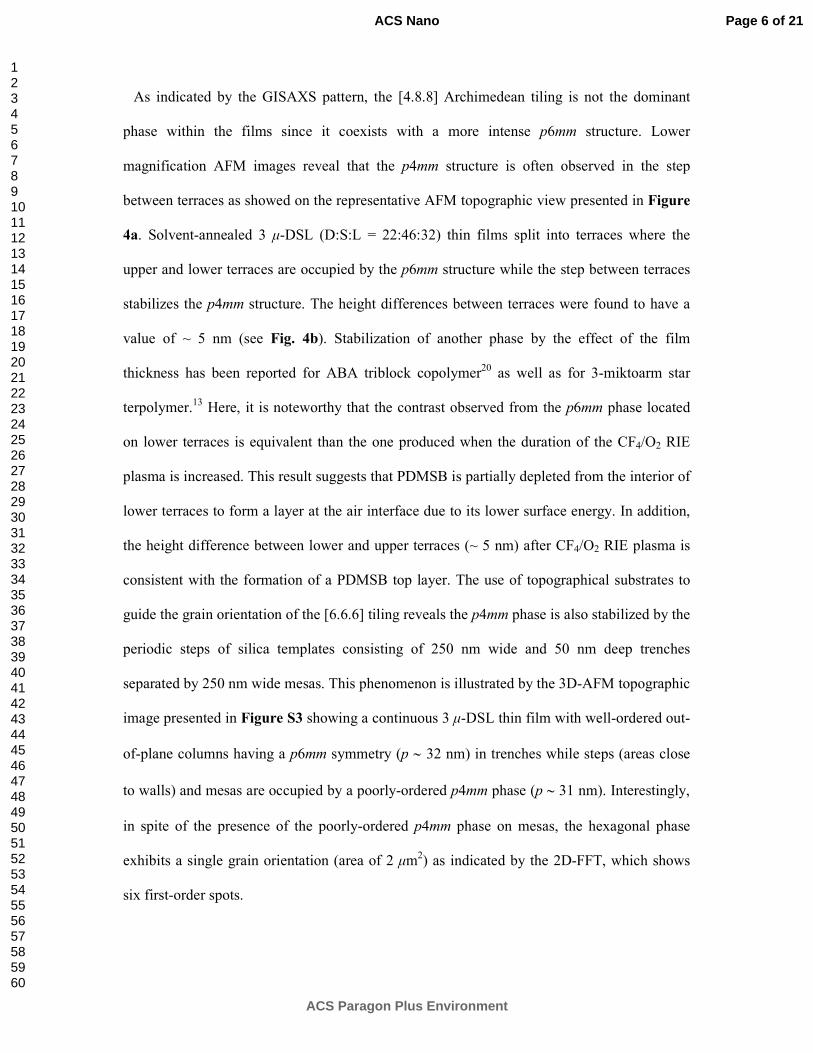
As indicated by the GISAXS pattern, the [4.8.8] Archimedean tiling is not the dominant
phase within the films since it coexists with a more intense p6mm structure. Lower
magnification AFM images reveal that the p4mm structure is often observed in the step
between terraces as showed on the representative AFM topographic view presented in Figure
4a. Solvent-annealed 3 µ-DSL (D:S:L = 22:46:32) thin films split into terraces where the
upper and lower terraces are occupied by the p6mm structure while the step between terraces
stabilizes the p4mm structure. The height differences between terraces were found to have a
value of ~ 5 nm (see Fig. 4b). Stabilization of another phase by the effect of the film
thickness has been reported for ABA triblock copolymer20 as well as for 3-miktoarm star
terpolymer.13 Here, it is noteworthy that the contrast observed from the p6mm phase located
on lower terraces is equivalent than the one produced when the duration of the CF4/O2 RIE
plasma is increased. This result suggests that PDMSB is partially depleted from the interior of
lower terraces to form a layer at the air interface due to its lower surface energy. In addition,
the height difference between lower and upper terraces (~ 5 nm) after CF4/O2 RIE plasma is
consistent with the formation of a PDMSB top layer. The use of topographical substrates to
guide the grain orientation of the [6.6.6] tiling reveals the p4mm phase is also stabilized by the
periodic steps of silica templates consisting of 250 nm wide and 50 nm deep trenches
separated by 250 nm wide mesas. This phenomenon is illustrated by the 3D-AFM topographic
image presented in Figure S3 showing a continuous 3 µ-DSL thin film with well-ordered out-
of-plane columns having a p6mm symmetry (p ∼ 32 nm) in trenches while steps (areas close
to walls) and mesas are occupied by a poorly-ordered p4mm phase (p ∼ 31 nm). Interestingly,
in spite of the presence of the poorly-ordered p4mm phase on mesas, the hexagonal phase
exhibits a single grain orientation (area of 2 µm2) as indicated by the 2D-FFT, which shows
six first-order spots.
Page 6 of 21
ACS Paragon Plus Environment
ACS Nano
123456789101112131415161718192021222324252627282930313233343536373839404142434445464748495051525354555657585960
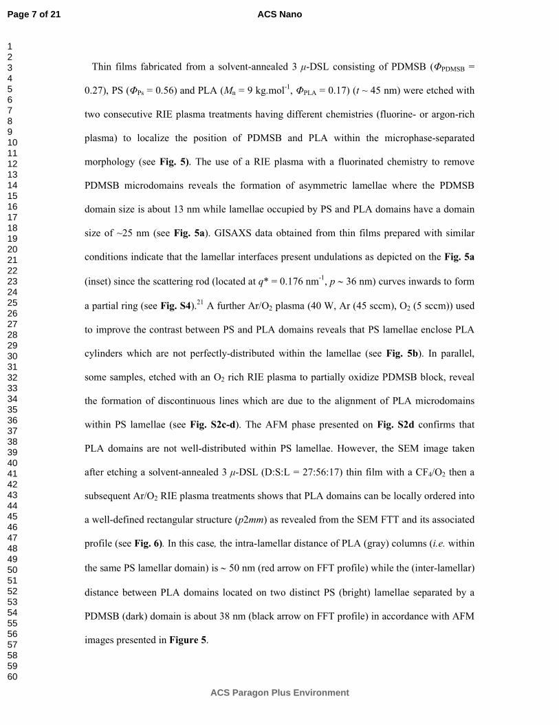
Thin films fabricated from a solvent-annealed 3 µ-DSL consisting of PDMSB (ΦPDMSB =
0.27), PS (ΦPs = 0.56) and PLA (Mn = 9 kg.mol-1, ΦPLA = 0.17) (t ~ 45 nm) were etched with
two consecutive RIE plasma treatments having different chemistries (fluorine- or argon-rich
plasma) to localize the position of PDMSB and PLA within the microphase-separated
morphology (see Fig. 5). The use of a RIE plasma with a fluorinated chemistry to remove
PDMSB microdomains reveals the formation of asymmetric lamellae where the PDMSB
domain size is about 13 nm while lamellae occupied by PS and PLA domains have a domain
size of ~25 nm (see Fig. 5a). GISAXS data obtained from thin films prepared with similar
conditions indicate that the lamellar interfaces present undulations as depicted on the Fig. 5a
(inset) since the scattering rod (located at q* = 0.176 nm-1, p ∼ 36 nm) curves inwards to form
a partial ring (see Fig. S4).21 A further Ar/O2 plasma (40 W, Ar (45 sccm), O2 (5 sccm)) used
to improve the contrast between PS and PLA domains reveals that PS lamellae enclose PLA
cylinders which are not perfectly-distributed within the lamellae (see Fig. 5b). In parallel,
some samples, etched with an O2 rich RIE plasma to partially oxidize PDMSB block, reveal
the formation of discontinuous lines which are due to the alignment of PLA microdomains
within PS lamellae (see Fig. S2c-d). The AFM phase presented on Fig. S2d confirms that
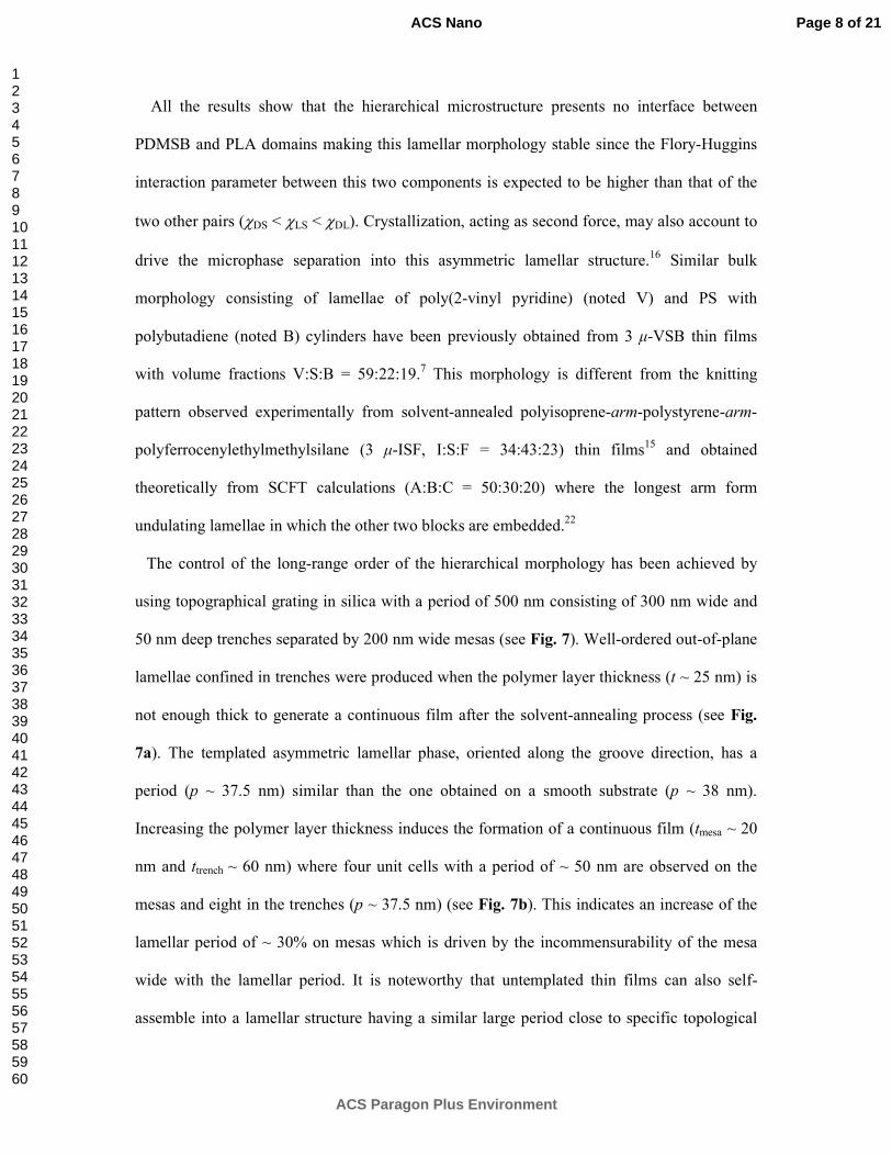
PLA domains are not well-distributed within PS lamellae. However, the SEM image taken
after etching a solvent-annealed 3 µ-DSL (D:S:L = 27:56:17) thin film with a CF4/O2 then a
subsequent Ar/O2 RIE plasma treatments shows that PLA domains can be locally ordered into
a well-defined rectangular structure (p2mm) as revealed from the SEM FTT and its associated
profile (see Fig. 6). In this case, the intra-lamellar distance of PLA (gray) columns (i.e. within
the same PS lamellar domain) is ∼ 50 nm (red arrow on FFT profile) while the (inter-lamellar)
distance between PLA domains located on two distinct PS (bright) lamellae separated by a
PDMSB (dark) domain is about 38 nm (black arrow on FFT profile) in accordance with AFM
images presented in Figure 5.
Page 7 of 21
ACS Paragon Plus Environment
ACS Nano
123456789101112131415161718192021222324252627282930313233343536373839404142434445464748495051525354555657585960
All the results show that the hierarchical microstructure presents no interface between
PDMSB and PLA domains making this lamellar morphology stable since the Flory-Huggins
interaction parameter between this two components is expected to be higher than that of the
two other pairs (χDS < χLS < χDL). Crystallization, acting as second force, may also account to
drive the microphase separation into this asymmetric lamellar structure.16 Similar bulk
morphology consisting of lamellae of poly(2-vinyl pyridine) (noted V) and PS with
polybutadiene (noted B) cylinders have been previously obtained from 3 µ-VSB thin films
with volume fractions V:S:B = 59:22:19.7 This morphology is different from the knitting
pattern observed experimentally from solvent-annealed polyisoprene-arm-polystyrene-arm-
polyferrocenylethylmethylsilane (3 µ-ISF, I:S:F = 34:43:23) thin films15 and obtained
theoretically from SCFT calculations (A:B:C = 50:30:20) where the longest arm form
undulating lamellae in which the other two blocks are embedded.22
The control of the long-range order of the hierarchical morphology has been achieved by
using topographical grating in silica with a period of 500 nm consisting of 300 nm wide and
50 nm deep trenches separated by 200 nm wide mesas (see Fig. 7). Well-ordered out-of-plane
lamellae confined in trenches were produced when the polymer layer thickness (t ~ 25 nm) is
not enough thick to generate a continuous film after the solvent-annealing process (see Fig.
7a). The templated asymmetric lamellar phase, oriented along the groove direction, has a
period (p ~ 37.5 nm) similar than the one obtained on a smooth substrate (p ~ 38 nm).
Increasing the polymer layer thickness induces the formation of a continuous film (tmesa ~ 20
nm and ttrench ~ 60 nm) where four unit cells with a period of ~ 50 nm are observed on the
mesas and eight in the trenches (p ~ 37.5 nm) (see Fig. 7b). This indicates an increase of the
lamellar period of ~ 30% on mesas which is driven by the incommensurability of the mesa
wide with the lamellar period. It is noteworthy that untemplated thin films can also self-
assemble into a lamellar structure having a similar large period close to specific topological
Page 8 of 21
ACS Paragon Plus Environment
ACS Nano
123456789101112131415161718192021222324252627282930313233343536373839404142434445464748495051525354555657585960
defect like the so-called chevron morphology where p is found to be about 51 nm (see Fig.
S5).
Conclusion
In summary, self-assembly of 3 µ-DSL thin films into ordered 2D Archimedean tilings and
hierarchical lamellar pattern is demonstrated. Excellent orientational order has been achieved
by templating the hierarchical lamellar morphology with topographical substrate. The
asymmetric lamellae produced from 3 µ-ABC provide a great convenience in lithography
application since many asymmetric lithographic line and space patterns are required and,
cannot be straightforwardly achieved by conventional block copolymer self-assembly. In
addition, the blending of the hierarchical lamellar structure with another 3 µ-DSL can be used
to tailor the periodicity of asymmetric lines. For instance, blending of 3 µ-DSL thin films
(D:S:L = 27:56:17) with 30 % wt. of 3 µ-DSL (D:S:L = 22:46:32) leads to a periodicity
change of the hierarchical lamellar pattern (pneat ~ 38 nm, pblend ~ 30 nm). A [6.6.6] tiling with
a period of 32 nm has been also produced from 3 µ-ABC. This “three-colored” pattern, which
cannot be obtained from a linear terpolymer, could be useful to produce dense array of nano-
objects such as dots, pillars or holes with utility in microelectronic patterning.
Experimental Section
Directed self-assembly of 3 µ-DSL thin films: Untemplated and templated 3 µ-DSL thin
films were spin-coated from THF solutions (1% wt.) and the film thickness was controlled by
varying the spin-coating speed (1.5-3 krpm). The self-assembly of 3 µ-DSL thin films was
promoted by exposing samples 3h to a continuous stream of THF vapor produced by bubbling
Page 9 of 21
ACS Paragon Plus Environment
ACS Nano
123456789101112131415161718192021222324252627282930313233343536373839404142434445464748495051525354555657585960
nitrogen gas through the liquid solvent as described previously.19 Untemplated film thickness
has been determined by AFM from scratched polymer area while templated film thickness has
been indirectly deduced from the mesa and trench height difference.
Topographical grating fabrication: The periodic topographical gratings were fabricated
using a Lloyd’s mirror interferometer with a 325 nm He-Cd laser beam. To transfer the
interference lithography pattern into the Si/50nm SiO2 layer, a trilayer resist stack
methodology was used. This trilayer was obtained by inserting a hard mask layer consisting of
a SiO2 thick film between a chemically-amplified negative resist resin and an anti-reflection
coating (ARC) layer. After development of the resist, the pattern was transferred into the hard
mask then into the ARC and finally into the SiO2 by a series of RIE steps to form a grating.
SEM and AFM Characterizations: Atomic force microscopy (AFM Dimension FastScan,
Bruker) was used in tapping mode to characterize the surface morphology of 3 µ-DSL thin
films. Silicon cantilevers (Fastcsan-A) with a typical tip radius of ∼ 5 nm were used. The
resonance frequency of the cantilevers was about 1.25 kHz. Prior to AFM measurement, 3 µ-
DSL thin films were etched with fluorine- or oxygen-rich RIE treatments in order to remove
the PDMSD phase or to enhance contrast of PLA domains on AFM phase images (plasma
conditions are: 40 W, 17 sccm CF4 and 3 sccm O2 or 90 W, 10 sccm O2 and 5 sccm Ar).
Scanning electron microscopy (SEM, JEOL 7800) was used in GBSH mode at an accelerating
voltage of 1 kV to take 3 µ-DSL thin films images.
GISAXS and SAXS Measurement: GISAXS measurements were performed on CRB-
BM02 beamline at the European Synchrotron Radiation Facilities (ESRF) in Grenoble using a
photon energy of 11 keV. The samples were positioned on a kappa-goniometer, for an
accurate control of the incident angle versus the film surface, chosen between the critical
angles of the polymer and the Si substrate. Horizontal and vertical widths of the beam focused
at the sample position were equal to 300 and 150 µm, respectively. GISAXS patterns were
Page 10 of 21
ACS Paragon Plus Environment
ACS Nano
123456789101112131415161718192021222324252627282930313233343536373839404142434445464748495051525354555657585960
recorded on a XPAD 2D pixel detector (960 × 560 pixels, 130 µm pixel size) placed at a
distance of 3080 mm from the sample.23 The intense incident and reflected beams were
stopped by a 2 mm wide Ta strip. To minimize air scattering the whole path of the scattered
beam was under vacuum apart from the nearest region around sample. With the incident beam
propagating along the x direction, the GISAXS images were recorded in the (qy, qz) plane
where qy and qz are the components of the scattering vector, related to the in-plane angle 2θf
and out-plane angle αf. GISAXS pattern, shown hereafter, was normalized with respect to the
incident beam intensity monitored by a front photomultiplier. SAXS experiments were
performed on the Dutch-Belgian Beamline (DUBBLE) at the European Synchrotron
Radiation Facility (ESRF) station BM26B in Grenoble.24 The energy of the x-ray beam was
11 keV, which corresponds to a wavelength of 1.127 Å. The 2D images were radially
averaged around the center of the primary beam in order to obtain the isotropic SAXS
intensity profiles. The scattering pattern from a specimen of silver behenate was used for the
calibration of the wavevector scale of the scattering curves. Finally, the data were normalized
to the intensity of the incident beam in order to correct for primary beam intensity
fluctuations.
Acknowledgements
The authors acknowledge support from Arkema and the Région Aquitaine. The ESRF and NWO are acknowledged for allocating beamtime at the Dutch-Belgian beamline (DUBBLE) for the SAXS experiments. D2AM French CRG Beamline is also acknowledged for allocating GISAXS beamtime. K. A. thanks Prof. C. A. Ross from MIT who provided topographical gratings. This work was performed within the framework of the Equipex ELORPrintTec ANR-10-EQPX-28-01 and the LabEx AMADEUS ANR-10-LABEX-0042-AMADEUS with the help of the French state Initiative d’Excellence IdEx ANR-10-IDEX-003-02 and the LCPO-Arkema INDUSTRIAL CHAIR “HOMERIC” ANR-13-CHIN-0002-01.
References
(1) Fujimoto, T.; Zhang, H.; Kazama, T.; Isono, Y.; Hasegawa, H.; Hashimoto, T.
Page 11 of 21
ACS Paragon Plus Environment
ACS Nano
123456789101112131415161718192021222324252627282930313233343536373839404142434445464748495051525354555657585960
Preparation and Characterization of Novel Star-Shaped Copolymers Having Three
Different Branches. Polymer (Guildf). 1992, 33, 2208–2213.
(2) Iatrou, H.; Hadjichristidis, N. Synthesis of a Model 3-Miktoarm Star Terpolymer.
Macromolecules 1992, 25, 4649–4651.
(3) Quirk, R. P.; Yoo, T.; Lee, B. Anionic Synthesis of Heteroarm, Star-Branched
Polymers. Scope and Limitations. J. Macromol. Sci. Part A 1994, 31, 911–926.
(4) Lambert, O.; Dumas, P.; Hurtrez, G.; Riess, G. Synthesis of an Amphiphilic Triarm
Star Copolymer Based on Polystyrene, Poly(ethylene Oxide) and Poly(ɛ-
Caprolactone). Macromol. Rapid Commun. 1997, 18, 343–351.
(5) Altintas, O.; Yankul, B.; Hizal, G.; Tunca, U. One-Pot Preparation of 3-Miktoarm Star
Terpolymers via Click [3 + 2] Reaction. J. Polym. Sci. Part A Polym. Chem. 2007, 45,
3588–3598.
(6) Hayashida, K.; Takano, A.; Arai, S.; Shinohara, Y.; Amemiya, Y.; Matsushita, Y.
Systematic Transitions of Tiling Patterns Formed by ABC Star-Shaped Terpolymers.
Macromolecules 2006, 39, 9402–9408.
(7) Hückstädt, H.; Göpfert, A.; Abetz, V. Synthesis and Morphology of ABC Heteroarm
Star Terpolymers of Polystyrene, Polybutadiene and poly(2-Vinylpyridine). Macromol.
Chem. Phys. 2000, 201, 296–307.
(8) Sioula, S.; Hadjichristidis, N.; Thomas, E. L. Direct Evidence for Confinement of
Junctions to Lines in an 3 Miktoarm Star Terpolymer Microdomain Structure.
Macromolecules 1998, 31, 8429–8432.
(9) Sioula, S.; Hadjichristidis, N.; Thomas, E. L. Novel 2-Dimensionally Periodic Non-
Constant Mean Curvature Morphologies of 3-Miktoarm Star Terpolymers of Styrene,
Isoprene, and Methyl Methacrylate. Macromolecules 1998, 31, 5272–5277.
(10) Takano, A.; Wada, S.; Sato, S.; Araki, T.; Hirahara, K.; Kazama, T.; Kawahara, S.;
Isono, Y.; Ohno, A.; Tanaka, N.; et al. Observation of Cylinder-Based Microphase-
Separated Structures from ABC Star-Shaped Terpolymers Investigated by Electron
Computerized Tomography. Macromolecules 2004, 37, 9941–9946.
(11) Yamauchi, K.; Takahashi, K.; Hasegawa, H.; Iatrou, H.; Hadjichristidis, N.; Kaneko,
T.; Nishikawa, Y.; Jinnai, H.; Matsui, T.; Nishioka, H.; et al. Microdomain
Morphology in an ABC 3-Miktoarm Star Terpolymer: A Study by Energy-Filtering
TEM and 3D Electron Tomography. Macromolecules 2003, 36, 6962–6966.
(12) Aissou, K.; Choi, H. K.; Nunns, A.; Manners, I.; Ross, C. a. Ordered Nanoscale
Archimedean Tilings of a Templated 3-Miktoarm Star Terpolymer. Nano Lett. 2013,
Page 12 of 21
ACS Paragon Plus Environment
ACS Nano
123456789101112131415161718192021222324252627282930313233343536373839404142434445464748495051525354555657585960
13, 835–839.
(13) Aissou, K.; Nunns, A.; Manners, I.; Ross, C. A. Square and Rectangular Symmetry
Tiles from Bulk and Thin Film 3-Miktoarm Star Terpolymers. Small 2013, 9, 4077–
4084.
(14) Gemma, T.; Hatano, A.; Dotera, T. Monte Carlo Simulations of the Morphology of
ABC Star Polymers Using the Diagonal Bond Method. Macromolecules 2002, 35,
3225–3237.
(15) Choi, H. K.; Gwyther, J.; Manners, I.; Ross, C. a. Square Arrays of Holes and Dots
Patterned from a Linear ABC Triblock Terpolymer. ACS Nano 2012, 6, 8342–8348.
(16) Aissou, K.; Mumtaz, M.; Fleury, G.; Portale, G.; Navarro, C.; Cloutet, E.; Brochon, C.;
Ross, C. a.; Hadziioannou, G. Sub-10 Nm Features Obtained from Directed Self-
Assembly of Semicrystalline Polycarbosilane-Based Block Copolymer Thin Films.
Adv. Mater. 2015, 27, 261–265.
(17) Rho, Y.; Aissou, K.; Mumtaz, M.; Kwon, W.; Pécastaings, G.; Mocuta, C.; Stanecu, S.;
Cloutet, E.; Brochon, C.; Fleury, G.; et al. Laterally Ordered Sub-10 Nm Features
Obtained From Directed Self-Assembly of Si-Containing Block Copolymer Thin
Films. Small 2015, 11, 6377–6383.
(18) Aissou, K.; Baron, T.; Kogelschatz, M.; Pascale, A. Phase Behavior in Thin Films of
Cylinder-Forming Diblock Copolymer: Deformation and Division of
Heptacoordinated Microdomains. Macromolecules 2007, 40, 5054–5059.
(19) Gotrik, K. W.; Hannon, A. F.; Son, J. G.; Keller, B.; Alexander-Katz, A.; Ross, C. A.
Morphology Control in Block Copolymer Films Using Mixed Solvent Vapors. ACS
Nano 2012, 6, 8052–8059.
(20) Knoll, A.; Horvat, A.; Lyakhova, K. S.; Krausch, G.; Sevink, G. J. A.; Zvelindovsky,
A. V; Magerle, R. Phase Behavior in Thin Films of Cylinder-Forming Block
Copolymers. Phys. Rev. Lett. 2002, 89, 035501.
(21) Smilgies, D.; Busch, P.; Papadakis, C. M.; Posselt, D. Characterization of Polymer
Thin Films with Small-angle X-ray Scattering under Grazing Incidence (GISAXS).
Synchrotron Radiat. News 2002, 15, 35–42.
(22) Li, S.; Qiu, W.; Zhang, L.; Liang, H. Nanostructures and Phase Diagrams of ABC Star
Triblock Copolymers in Pore Geometries. J. Chem. Phys. 2012, 136, 124906.
(23) Berar, J.-F.; Boudet, N.; Breugnon, P.; Caillot, B.; Chantepie, B.; Clemens, J.-C.;
Delpierre, P.; Dinkespiller, B.; Godiot, S.; Meessen, C.; et al. XPAD3 Hybrid Pixel
Detector Applications. Nucl. Instruments Methods Phys. Res. Sect. A Accel.
Page 13 of 21
ACS Paragon Plus Environment
ACS Nano
123456789101112131415161718192021222324252627282930313233343536373839404142434445464748495051525354555657585960
Spectrometers, Detect. Assoc. Equip. 2009, 607, 233–235.
(24) Bras, W.; Dolbnya, I. P.; Detollenaere, D.; van Tol, R.; Malfois, M.; Greaves, G. N.;
Ryan, A. J.; Heeley, E. Recent Experiments on a Small-Angle/wide-Angle X-Ray
Scattering Beam Line at the ESRF. J. Appl. Crystallogr. 2003, 36, 791–794.
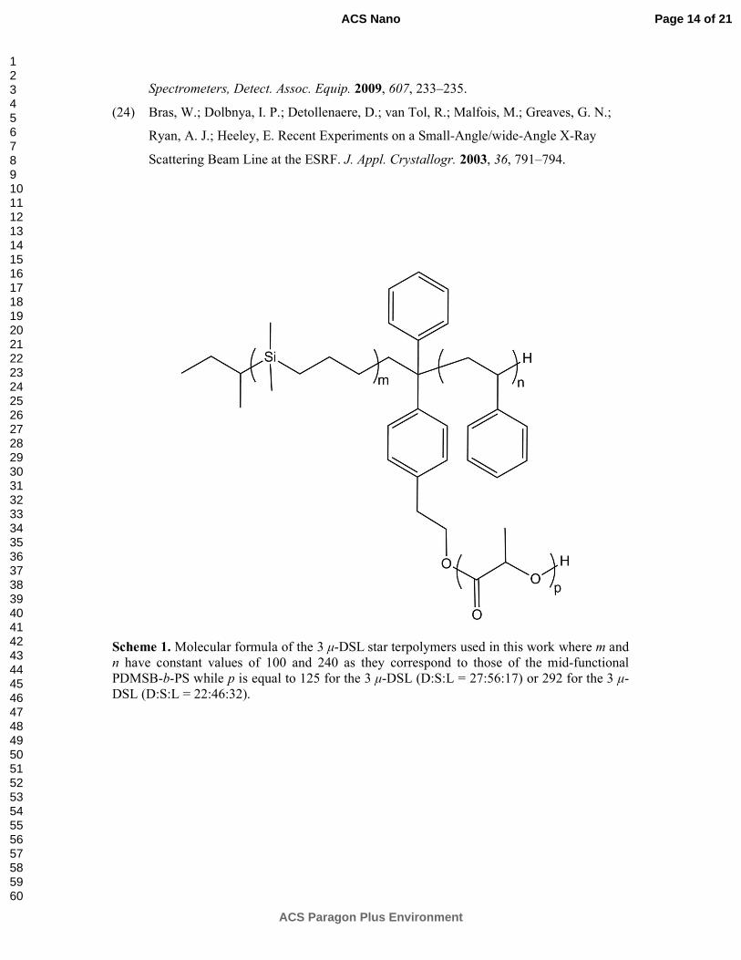
Scheme 1. Molecular formula of the 3 µ-DSL star terpolymers used in this work where m and n have constant values of 100 and 240 as they correspond to those of the mid-functional PDMSB-b-PS while p is equal to 125 for the 3 µ-DSL (D:S:L = 27:56:17) or 292 for the 3 µ-DSL (D:S:L = 22:46:32).
Page 14 of 21
ACS Paragon Plus Environment
ACS Nano
123456789101112131415161718192021222324252627282930313233343536373839404142434445464748495051525354555657585960
Figure 1. AFM topographic view of a solvent-annealed 3 µ-DSL (D:S:L = 22:46:32) thin film (t ~ 45 nm) treated by a CF4/O2 RIE plasma which includes two columnar morphologies indexed with a p6mm or p4mm symmetry. The dashed line delimits the regions occupied by the different phases. Schematic models showing (top) the p4mm and (bottom) the p6mm microstructures corresponding to the [4.8.8] and [6.6.6] tilings, respectively. Scale bar: 250 nm.
Figure 2. GISAXS pattern of a solvent-annealed 3 µ-DSL (D:S:L = 22:46:32) thin film (t ~ 45 nm) treated by a CF4/O2 RIE plasma. Black and red arrows on the GISAXS pattern indicate the first-peak order position of the p6mm and p4mm phases and are noted q* and q**, respectively. Higher-order peaks of the p6mm phase are also indexed.
Page 15 of 21
ACS Paragon Plus Environment
ACS Nano
123456789101112131415161718192021222324252627282930313233343536373839404142434445464748495051525354555657585960
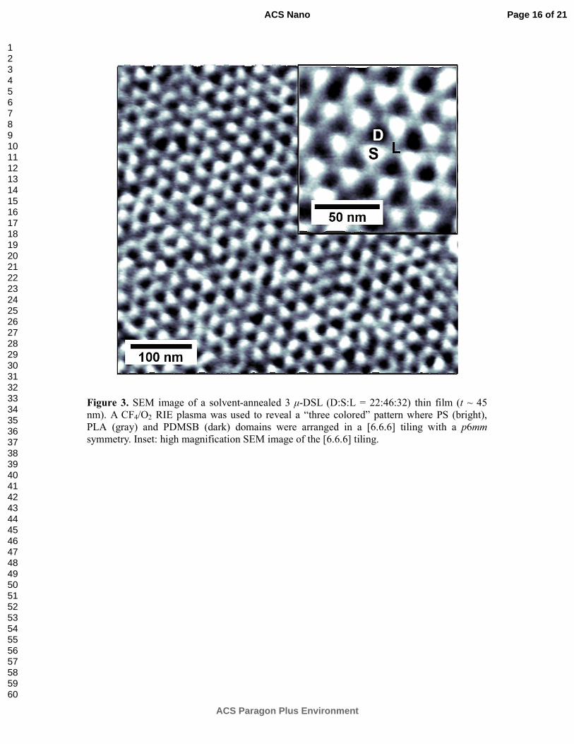
Figure 3. SEM image of a solvent-annealed 3 µ-DSL (D:S:L = 22:46:32) thin film (t ~ 45 nm). A CF4/O2 RIE plasma was used to reveal a “three colored” pattern where PS (bright), PLA (gray) and PDMSB (dark) domains were arranged in a [6.6.6] tiling with a p6mm symmetry. Inset: high magnification SEM image of the [6.6.6] tiling.
Page 16 of 21
ACS Paragon Plus Environment
ACS Nano
123456789101112131415161718192021222324252627282930313233343536373839404142434445464748495051525354555657585960
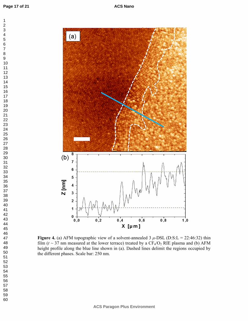
Figure 4. (a) AFM topographic view of a solvent-annealed 3 µ-DSL (D:S:L = 22:46:32) thin film (t ~ 37 nm measured at the lower terrace) treated by a CF4/O2 RIE plasma and (b) AFM height profile along the blue line shown in (a). Dashed lines delimit the regions occupied by the different phases. Scale bar: 250 nm.
Page 17 of 21
ACS Paragon Plus Environment
ACS Nano
123456789101112131415161718192021222324252627282930313233343536373839404142434445464748495051525354555657585960
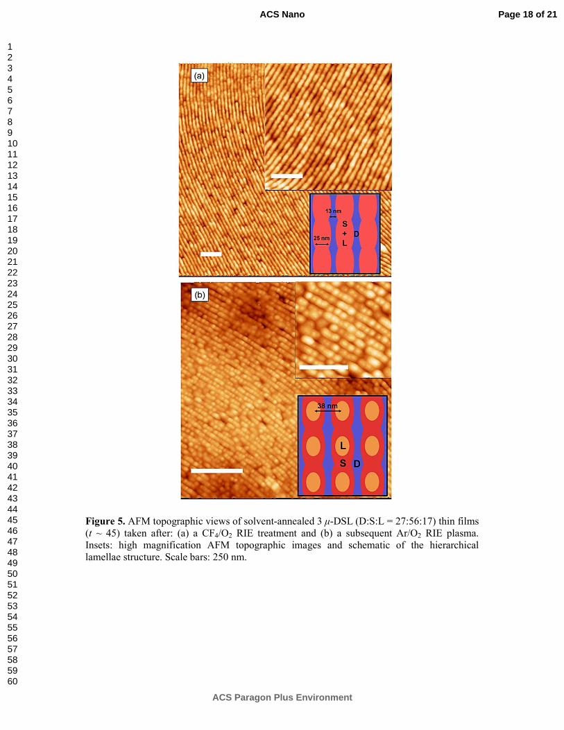
Figure 5. AFM topographic views of solvent-annealed 3 µ-DSL (D:S:L = 27:56:17) thin films (t ~ 45) taken after: (a) a CF4/O2 RIE treatment and (b) a subsequent Ar/O2 RIE plasma. Insets: high magnification AFM topographic images and schematic of the hierarchical lamellae structure. Scale bars: 250 nm.
Page 18 of 21
ACS Paragon Plus Environment
ACS Nano
123456789101112131415161718192021222324252627282930313233343536373839404142434445464748495051525354555657585960
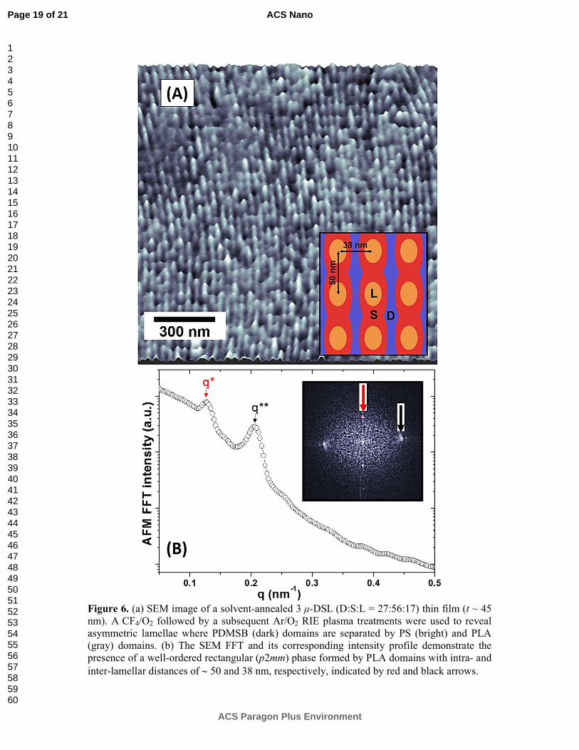
Figure 6. (a) SEM image of a solvent-annealed 3 µ-DSL (D:S:L = 27:56:17) thin film (t ~ 45 nm). A CF4/O2 followed by a subsequent Ar/O2 RIE plasma treatments were used to reveal asymmetric lamellae where PDMSB (dark) domains are separated by PS (bright) and PLA (gray) domains. (b) The SEM FFT and its corresponding intensity profile demonstrate the presence of a well-ordered rectangular (p2mm) phase formed by PLA domains with intra- and inter-lamellar distances of ∼ 50 and 38 nm, respectively, indicated by red and black arrows.
Page 19 of 21
ACS Paragon Plus Environment
ACS Nano
123456789101112131415161718192021222324252627282930313233343536373839404142434445464748495051525354555657585960
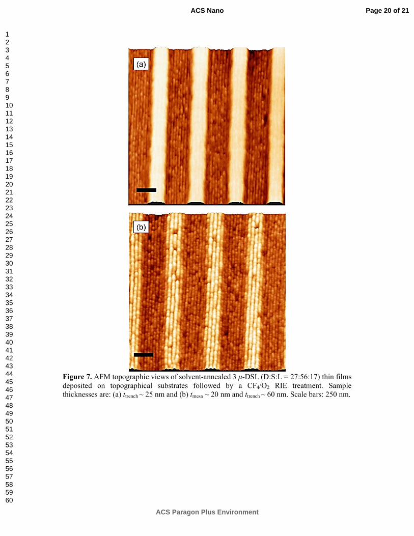
Figure 7. AFM topographic views of solvent-annealed 3 µ-DSL (D:S:L = 27:56:17) thin films deposited on topographical substrates followed by a CF4/O2 RIE treatment. Sample thicknesses are: (a) ttrench ~ 25 nm and (b) tmesa ~ 20 nm and ttrench ~ 60 nm. Scale bars: 250 nm.
Page 20 of 21
ACS Paragon Plus Environment
ACS Nano
123456789101112131415161718192021222324252627282930313233343536373839404142434445464748495051525354555657585960
Use for TOC only
Page 21 of 21
ACS Paragon Plus Environment
ACS Nano
123456789101112131415161718192021222324252627282930313233343536373839404142434445464748495051525354555657585960


![Designing Dendrimer and Miktoarm Polymer Based Multi ...€¦ · and carbon nanotubes [51,52], and among inorganics are quantum dots [53,54], silica [55,56] and gold nanoparticles](https://img.pdfslide.us/doc/110x75/5fa0499807b6d03896211fef/designing-dendrimer-and-miktoarm-polymer-based-multi-and-carbon-nanotubes-5152.jpg)