Embed Size (px)
Citation preview

Flipchip bonding with solder dippingM. J. Brady and A. Davidson Citation: Review of Scientific Instruments 56, 1459 (1985); doi: 10.1063/1.1138505 View online: http://dx.doi.org/10.1063/1.1138505 View Table of Contents: http://scitation.aip.org/content/aip/journal/rsi/56/7?ver=pdfcov Published by the AIP Publishing Articles you may be interested in Study of Electromigration of flipchip solder joints using Kelvin probes AIP Conf. Proc. 945, 194 (2007); 10.1063/1.2815779 Effect of Al-trace degradation on Joule heating during electromigration in flip-chip solder joints Appl. Phys. Lett. 90, 082103 (2007); 10.1063/1.2644061 Study of void formation due to electromigration in flip-chip solder joints using Kelvin bump probes Appl. Phys. Lett. 89, 032103 (2006); 10.1063/1.2226989 Hydrogen plasmas for flux free flipchip solder bonding J. Vac. Sci. Technol. A 8, 1503 (1990); 10.1116/1.576865 Solder bump height dependence of Josephson chiptocard interconnection inductance using flipchip bondingtechnique J. Appl. Phys. 54, 5282 (1983); 10.1063/1.332757
This article is copyrighted as indicated in the article. Reuse of AIP content is subject to the terms at: http://scitationnew.aip.org/termsconditions. Downloaded to IP:
128.42.202.150 On: Tue, 25 Nov 2014 11:16:40

NOTES BRIEF contributions in any field of instrumentation or technique within the scope of the journal should be submitted for this section. Contributions should in general not exceed 500 words.
Flip-chip bonding with solder dipping M. J. Brady and A. Davidson
IBM Thomas J. Watson Research Center, Yorktown Heights, New York 10598
(Received 11 March 1985; accepted for publication 27 March 1985)
We report a simple technique for making flip-chip contacts. The equipment required, in addition to a small-scale photoresist dean room, is a beaker of molten solder.
Flipping a chip over to make connections between it and a substrate has been in use for several years in certain commercial technologies. The same technique can also be of advantage in small-scale applications and one-of-a-kind experiments. This type of contact offers low inductance, repeatability, and controlled characteristic impedances for microwave applications. At low temperatures flip-chip bonding can be achieved with superconducting materials to allow for SQUID magnetometers, and/or very low losses. Reliable connections to the flipped chip have, however, required esoteric materials or techniques 1-3 which may inhibit its use in smal11aboratories. In this report we show how flipchip bonding can be achieved with the addition of only a hot plate and solder pot to typical small scale photolithographic clean-room facilities.
The trick in flip-chip bonding is to provide a raised bump on a pad on a substrate to make contact to the pads on the chip to be bonded. If the substrate is transparent, alignment can be done by hand, while looking through a low power microscope. An accuracy of better than 20 p can be routinely achieved. Similar results can be produced on opaque substrates if alignment marks are provided. Moskowitz, Faris, and Davidson l made such a system, with alignment marks, in which the bumps were formed by soldering copper spheres 100 I" in diameter to pads on the substrate. This approach allowed for repeated removal and reattachment of the chip because of the hardness of the copper balls. Recently, Schmid and Melchior2 presented a microwave flip-chip package that used plated indium for contact to the chip. Although this technique allowed a permanent soldered connection by reflowing the indium in a reducing atmosphere, it required the use of plating equipment to build up the indium layer in the first place. Our contribution to this technology is the observation that uniform bumps of solder can be placed on pads by dipping the substrate in molten solder at the right temperature. Further, the solder can be limited to the desired areas with photoresist.
We have made solder-dip flip-chip connections to sapphire, quartz, and Corning glass substrates.4 We blanket
coated the substrate with 5000 A of copper (with a thin layer of chromium first to promote adhesion). Then, using standard photoresist techniques we patterned the desired lines and pads by chemical etching. If it is acceptable that aU remaining metal on the substrate gets coated with solder, the chip can be dipped as is. The idea behind dipping is that surface tension will hold more solder on a large copper area than on a small one. Hence, pads will have a thicker mound of solder than narrow lines. We typically used 100-1" pads and 20-1" lines. The finished pads had about 10 p of solder after dipping, and the lines only 2 or 31'" We used the eutectic tin/lead solder (60/40 wt. %) melted without flux in a beaker on a laboratory hot plate. This composition of tin/ lead has a melting point of about 180°C, but is heated to 220 °C to ensure good wetting properties. The patterned substrate is first dipped into a liquid flux bath.5 Then, using tweezers or tongs, it is dipped in the Sn/Pb solder bath. If the
FIG. I. Oblique angle (45°) SEM of a lOO-IL-wide pad with a 1O-Il-high solder bump. Note the much smaller height of solder on the line leading to the pad.
1459 Rev. Sci.lnstrum. 56 (7), July 1985 0034-6748/85/071459-02$01.30 © 1985 American Institute of PhysIcs 1459 This article is copyrighted as indicated in the article. Reuse of AIP content is subject to the terms at: http://scitationnew.aip.org/termsconditions. Downloaded to IP:
128.42.202.150 On: Tue, 25 Nov 2014 11:16:40
solder is hot enough there will be uniform wetting of the metal pattern, but no adhesion to the substrate. There may be occasional small solder balls visible on the clear substrate, but they are easily removed by poking with a toothpick. After rinsing, the substrate is ready for the mounting of the chip. Figure 1 is a SEM of such a pad clearly showing the thickness differential between lines and pads. Using low magnification optics, the substrate is aligned over the chip through the back side and pressed into place. Bonding of the chip to the pads on the substrate is then completed by either mechanical pressure as in Moskowitz et al. 1 or thermal refiow. 2
For cases where only a portion of the metal. on the patterned substrate is to receive the solder, an additional step is required. After the copper has been patterned, a second photoresist layer is spun on and exposed. Developing then removes the photoresist only from those areas that are to receive solder. The photoresist is postbaked, and the substrate is ready for solder dipping as before. If pin holes in the photo-
resist are a problem it may help to oxidize the copper before application of the photoresist.
Solder dipping s substrate with photoresist requir~ some practice. If the dip takes too long, the resist will deteriorate, exacerbating the pin hole problem, and eventual.ly polymerizing the resist. If the dip is too fast, uniform wetting will not be achieved. For our typical I-in. substrates we found a 1 or 2-s dip to work well, divided about evenly between insertion, a brief wait, and then withdrawal.
We thank E. Liniger for the SEM photographs, and acknowledge D. Frank for helpful discussions.
'P. A. Moskowitz, S. M. Faris, and A. Davidson, IEEE Trans. MAG-19, 503 (1983).
2p. Schmid and H. Melchior, Rev. Sci. Instrum. 55, 1854 (1984). 3L. D. Comerford and M. J. Brady, Elect. Lett. 18,629 (1982). 'Coming Glass Co., Coming. NY. 'We used Supersafe No. 30, from the Superior Flux and Mfg. Co., Cleveland,OH.
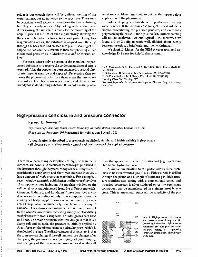
High-pressure cell closure and pressure connector Kenneth E. Newmana)
Department of Chemistry, Simon Fraser University, Burnaby, British Columbia, Canada V5A J S6
(Received 27 February 1985; accepted for publication 3 April 1985)
A modification is described to a previously published, simple, and highly reliable high-pressure cell closure so as to allow ready control and monitoring of the applied pressure.
There have been many descriptions of high-pressure cells, closures, windows, and electrical feedthroughs published in the literature through the years. Many of these designs are of considerable complexity and their manufacture involves a large amount of high-precision machining. For example, a recent window assembly published in the literature I involves 1.1 components (not including the sapphire window or the cell body) to be manufactured from five different materials. Claesson, Malmrud, and Lundgren2
•3 have described a win
dow assembly consisting of only three components (not including cell body, sapphire window, or commerciaUy available 0 rings) which is immensely reliable and truly easy to assemble. The c1.osures used in this cell are similar in concept to the window assemblies consisting simply of dose-fitting steel pistons with two O-ring seals. This design has been used to 8 kbar. The major problem with this design is that it is a clamp cell and as such, the pressure is initially applied by direct force on the piston (using a hydraulic press) which is then locked in place. The disadvantages of this system is that the pressure can change if the cell temperature changes after clamping, the pressure cannot be monitored continuously, and changing of the pressure requires removal of the cell
from the apparatus to which it is attached (e.g., spectrometer) to the hydraulic press.
A simple modification to the piston allows these problems to be circumvented (see Fig. 1). Either a hole is drilled through the piston and a l.ength of standard! in. high-pressure stainless-steel tubing with a conventional coned and threaded connector is silver soldered on or the equivalent component can be manufactured in stainless steel in one piece. This arrangement retains all the simplicity of the pis-
FiG. 1. High-pressure cell closure and pressure transmitting tube. (A) Coned and threaded high-pressure connector, (BI high-pressure stainless-steel tubing, (C) supporting screw, (DI piston body, (EI cell body, (F) 0 ring.
1460 Rev. Scl.lnstrum. 56 (7), July 1985 0034-6748/85/071460-02$01.30 @ 1985 American Institute of Physics 1460 This article is copyrighted as indicated in the article. Reuse of AIP content is subject to the terms at: http://scitationnew.aip.org/termsconditions. Downloaded to IP:
128.42.202.150 On: Tue, 25 Nov 2014 11:16:40