Embed Size (px)
Citation preview
205788
Final ReportGrant NAG 5 2609
'- /) / :...--
University of New Mexico
June 30, 1996
Contents
1 Summary
2 Special Purpose VLSI Technology
2.1 CCSDS Reed Solomon Decoder ........................
2.2 Lossless Decompresser .............................
2.3 Lossy Data Compression ............................
2.4 SEU Fault Tolerant Architectures .......................
2.5 Binary Tree Structured Logic .........................
2.6 Global Positioning System ...........................2.7 1773 Transceiver ................................
2.8 Correlators ...................................
3 High Performance Data Compression
3.1 Rice Algorithm Overview ............................
4 VLSI Implementations
4.1 The First Chip Set ...............................
4.1.1 Universal Source Encoder .......................
4.1.2 Universal Source Decoder .......................
4.2 Universal Source Encoder for Space ......................
4.2.1 USES Coding Enhancements ......................
4.2.2 USES System Improvements ......................
5 Data Compression VLSI Details
6 Delivery of VLSI to the Government
7 Commercial Technology Transfer
7.1 Broadcom Corporation .............................
7.2 1773 Transceiver ................................
7.3 Correlator ....................................
1
1
1
2
2
2
3
4
4
4
4
5
6
6
6
7
8
8
8
9
10
11
11
12
12
https://ntrs.nasa.gov/search.jsp?R=19970040586 2018-06-10T17:30:19+00:00Z
1 Summary
Research work in the providing radiation tolerant electronics to NASA and the commercial
sector is reported herein. There are four major sections to this report.
Special Purpose VLSI Technology. This section discusses the status of the VLSI
projects as well as the new background technologies that have been developed.
Lossless Data Compression Results This section provides the background and
direction of new data compression pursued under this grant.
Commercial Technology Transfer An itemization of the commercial technology
transfer is presented.
Delivery of VLSI to the Government A solution and progress report is given
that shows how the Government and Government contractors are gaining access to
the technology that has been developed by the MRC.
2 Special Purpose VLSI Technology
The research projects currently active include:
2.1 CCSDS Reed Solomon Decoder
The radiation tolerant CCSDS Reed Solomon decoder logic design has been complete for
some time. The decoder can operate in two modes, one for flight and the other as a high
speed ground based decoder. It was decided to configure the decoder design to operate at a
rate close to 600 Mbits/sec (75 Mhz input symbol rate). This can be done by implementing
the design in a modern IC process such as the 0.5 micron HP process. With the decision
to pursue the HP process, the decoder transistor logic is being resized for new process.
One patent is being submitted. A copy of this disclosure is included herein in the section
SEU Fault Tolerant Architectures.
2.2 Lossless Decompresser
All fundamental research has been completed. The demonstration processor is being de-
signed with all the logic completed, with the only major section not simulated being the
input control state machine. This section has been redesigned to eliminate a critical timing
path. All data paths have been simulated. Two-thirds of the chip layout as been completed
on a total area basis.
2.3 Lossy Data Compression
The lossy data compression algorithm architecture is complete with the logic design in
progress. The research in this processor has resulted in an architecture that a limited num-
ber of unique cells. This allows for either a full-custom or a standard cell implementation.
It is planned to implement this processor in the HP 0.5 micron CMOS process.
2.4 SEU Fault Tolerant Architectures
When a charged particle impacts electronics, it is possible that a node value can be changed;
this is called an upset. Previous SEU technology protects logic with hardware (extra
transistors or capacitance) from experiencing an upset when a charged particle impacts
electronics. The disadvantage with this approach is that SEU tolerant electronics can
require a significantly large amount of area. Therefore, a complete circuit comprised only
of SEU electronics can be significantly large.
Non-SEU tolerant electronics can experience upsets upon impact of a charged particle,
however, these circuits are much smaller and more dense than SEU tolerant electronics.
Time redundancy is a recognized means to protect circuits and systems from soft or
transient errors. An operation is repeated, at least twice, until the resulting answer is the
same. If a transient error due to an SEU is present, then it will be tolerated.
It is assumed in this discussion that if a process requires N clock times to complete,
than an SEU particle does not occur more often than MxN, where N is greater than 1.
Invention
The final circuit consists of two portions
• SEU Immune control portion which is comprised of SEU tolerant electronics described
in patents 5,406,513 and 5,418,473..
• Digital processor, which is not SEU immune
The SEU control portion is immune to charged particles and therefore will operate
correctly in a charged particle environment. The size of the control portion is relatively
large in comparison to non-SEU tolerant logic, but since the controller is relatively small,
the overall impact to the total circuit is small. The digital processor consists of non-SEU
immune logic and implements control and data path functions. Any control function in the
digital processor has to be reset-able by the SEU immune controller.
The operation consists of the following:
1. Present new data to digital processor
2. Record the output
3. Present the same data to digital processor
2
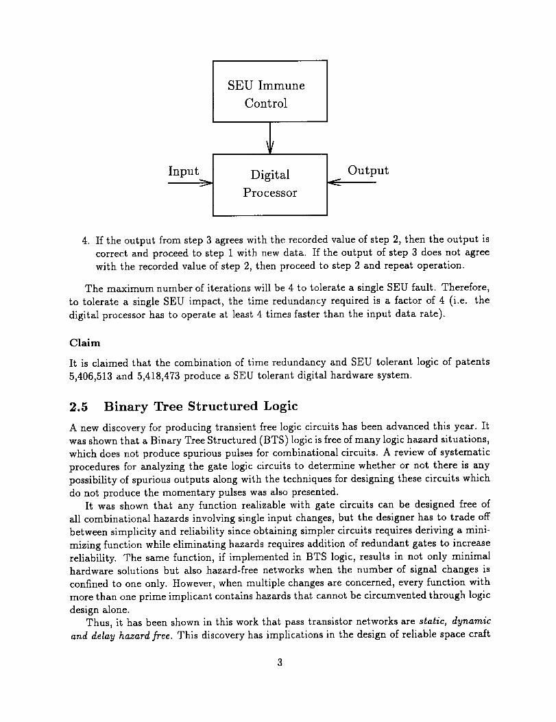
SEU Immune
Control
Input _] DigitalProcessor
Output
4. If the output from step 3 agrees with the recorded value of step 2, then the output is
correct and proceed to step 1 with new data. If the output of step 3 does not agree
with the recorded value of step 2, then proceed to step 2 and repeat operation.
The maximum number of iterations will be 4 to tolerate a single SEU fault. Therefore,
to tolerate a single SEU impact, the time redundancy required is a factor of 4 (i.e. the
digital processor has to operate at least 4 times faster than the input data rate).
Claim
It is claimed that the combination of time redundancy and SEU tolerant logic of patents
5,406,513 and 5,418,473 produce a SEU tolerant digital hardware system.
2.5 Binary Tree Structured Logic
A new discovery for producing transient free logic circuits has been advanced this year. It
was shown that a Binary Tree Structured (BTS) logic is free of many logic hazard situations,
which does not produce spurious pulses for combinational circuits. A review of systematic
procedures for analyzing the gate logic circuits to determine whether or not there is any
possibility of spurious outputs along with the techniques for designing these circuits which
do not produce the momentary pulses was also presented.
It was shown that any function realizable with gate circuits can be designed free of
all combinational hazards involving single input changes, but the designer has to trade off
between simplicity and reliability since obtaining simpler circuits requires deriving a mini-
mizing function while eliminating hazards requires addition of redundant gates to increase
reliability. The same function, if implemented in BTS logic, results in not only minimal
hardware solutions but also hazard-free networks when the number of signal changes is
confined to one only. However, when multiple changes are concerned, every function with
more than one prime implicant contains hazards that cannot be circumvented through logic
design alone.
Thus, it has been shown in this work that pass transistor networks are static, dynamic
and delay hazard free. This discovery has implications in the design of reliable space craft
3
electronics.
2.6 Global Positioning System
There has been considerable interaction with JPL and it was decided by JPL that this
project be postponed until more GPS research at JPL can be performed.
2.7 1773 Transceiver
The optical transceiver processor was completed this year. Testing was accomplished at
GSFC in their flight demonstration system. Honeywell Corporation will begin to manufac-
ture and market this device.
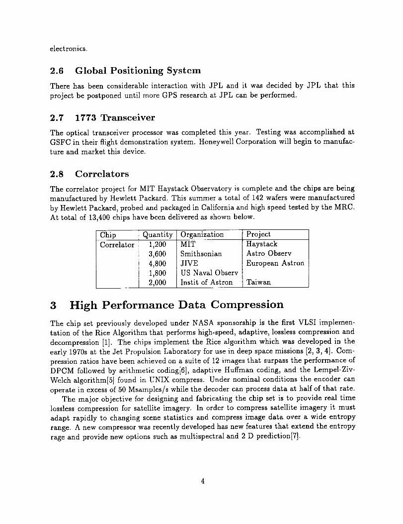
2.8 Correlators
The correlator project for MIT Haystack Observatory is complete and the chips are being
manufactured by Hewlett Packard. This summer a total of 142 wafers were manufactured
by Hewlett Packard, probed and packaged in California and high speed tested by the MRC.
At total of 13,400 chips have been delivered as shown below.
Chip Quantity Organization Project
Correlator 1,200
3,600
4,800
1,800
2,000
MIT
Smithsonian
JIVE
US Naval Observ
Instit of Astron
HaystackAstro Observ
European Astron
Taiwan
3 High Performance Data Compression
The chip set previously developed under NASA sponsorship is the first VLSI implemen-
tation of the Rice Algorithm that performs high-speed, adaptive, lossless compression and
decompression [1]. The chips implement the Rice algorithm which was developed in the
early 1970s at the Jet Propulsion Laboratory for use in deep space missions [2, 3, 4]. Com-
pression ratios have been achieved on a suite of 12 images that surpass the performance of
DPCM followed by arithmetic coding[6], adaptive Huffman coding, and the Lempel-Ziv-
Welch algorithm[5] found in UNIX compress. Under nominal conditions the encoder can
operate in excess of 50 Msamples/s while the decoder can process data at half of that rate.
The major objective for designing and fabricating the chip set is to provide real time
lossless compression for satellite imagery. In order to compress satellite imagery it must
adapt rapidly to changing scene statistics and compress image data over a wide entropy
range. A new compressor was recently developed has new features that extend the entropy
rage and provide new options such as multispectral and 2 D prediction[7].
4
3.1 Rice Algorithm Overview
The Rice algorithm is a lossless compression method that is rapidly adaptive and efficient
over a wide range of entropy conditions. The structure of the algorithm can best be
understood through the following argument. Assume that a particular encoder has, for
.example, 11 different Huffman codes to choose from. Each Huffman code is designed for a
particular entropy range. The first codebook might be designed for an expected codeword
length of 2 bits, while the next one might be designed for an expected codeword length of
3 bits, and so on in integer increments of one bit. By applying each of the 11 codebooks
to the same data block of size J, and then choosing the codebook that produced the best
compression would allow the coder to cover a wide entropy range: approximately 1.5 bits
through 12.5 bits. By deciding which coder was the winner on a block by block basis, the
coder would be adaptive to changes in data entropy.
One of Robert F. Rice's accomplishments was develop a compression algorithm that
requires no codebooks [1], yet provides equivalent performance to the multiple Huffman
codebook approach just described. The equivalence is only true for sources that have a
Laplacian distribution. Fortunately, for many types of sampled data, especially imagery,
the output from DPCM can be well modeled as a Laplacian distribution. The Rice algo-
rithm has been shown mathematically to provide equivalent performance to using multiple,
parallel Huffman codes, this was supported by extensive simulations [8]. An intuitive feel for
this equivalence can be obtained by understanding two major components of the algorithm:
a comma code Rice calls the Fundamental Sequence (FS), and sample splitting.
The Fundamental Sequence (FS) is a comma code that has the property that a value
m has a corresponding codeword that is made up of m zeros followed by a '1'. Since each
codeword is uniquely defined by simply knowing the input value, codebooks are not needed.
A value of 7, for example, will be coded with 7 zeros followed by a '1'.
Sample splitting is a technique that assumes that the k least significant bits for every
input in a block are random, and therefore, can not be compressed. The Rice algorithm
uses sample splitting in the following manner. First, it assumes the incoming N bit data
can be compressed without splitting off any bits. The FS code is used on the incoming
data words. Next, it assumes that the least significant bits are random and then uses the
same FS code on the N-1 remaining bits. The least significant bits are then concatenated
and sent after the FS coded bits. Next, 2 bits (k=2) are assumed to be random, while the
N-2 remaining most significant bits are FS coded. Sample splitting the least significant k
bits for k = [0..10] combined with FS coding the N-k most significant bits define eleven of
the twelve code options used in this chip set.
For low entropy data, direct coding of the data, without sample splitting, would pro-
duce the fewest number of coded bits. Higher entropy data will be more efficiently coded
by using sample splitting. This reaffrms the assumption that as entropy increases the
randomness (or information content) in the k least-significant bits prohibits compression.
Therefore, using successive split bits combined with FS coding is equivalent to using Huff-
man codebooks that are designed for successive integer steps in entropy. Due to the simple
structure of the FS code, however, no actual codebook is necessary for each code option.
4 VLSI Implementations
The first chip set that employs the Rice algorithm was fabricated in 1991 and has since
become a commercially available product [9]. A second generation Rice algorithm based
encoder has been designed and is being fabricated in 1993 as a space qualified gate-array
[7]. The new encoder has been baselined for the Landsat-7 satellite project.
4.1 The First Chip Set
The first Rice chip set was fabricated in a 1 micron CMOS process. It uses a cell-based,
structured-custom approach. In such an approach, engineers make specific effort to analyze
data flow while developing the chip architecture. Layout technicians often abut the cellsto minimize the amount of interconnect. Because of the structure of the Fundamental
Sequence, no look-up tables were needed on either chip. The combined memory on both
chips is only 340 bytes. The die size for each is 5 mm on a side, but neither chip fills up
its core area.
4.1.1 Universal Source Encoder
The encoder's chip name is "USE", an acronym which stands for Universal Source Encoder.
USE has a fully pipelined architecture; after 64 clock cycles, data is available for output.
It can continuously accept new data and process every sample in one clock cycle.
The chip architecture and the generic Rice architecture differ in three ways. First, on the
chip, differential pulse code modulation (DPCM) and mapper functions were implemented
in one hardware block. Second, the winner select section was broken up into two sections
for the chip: the bit counts section and the winner select section. The bit counts section is
the largest single block on the chip. It calculates the number of bits that will be required
to code the input block (16 samples) for each of the 12 coding options. The winner select
block selects which of the options will produce the smallest number of coded bits and
also perform calculations needed for the coding sections. The final difference between the
VLSI implementation and the generic architecture is sharing of hardware among 12 coding
options: only 2 hardware blocks are necessary (FS and K/Default). Control is distributed
throughout the chip, but is mainly found in the input control section "InCntrl" and the
two coding blocks.
The total amount of memory on the USE chip is only 130 bytes. The largest memory is
the FIFO shown on the block diagram, 56 bytes, that holds the sigma values while the bit
counts section calculates how many bits each of the options will take to encode the block.
The K/Default section consists of a barrel shifter and control section that performs the
packing of k split bits (or default data) into an output word size of 16 bits.
The data formatter concatenates the split bits with FS coded bits. It also prepends the
4 ID bits that specify which code option performed the coding. The output of the chip is
a 16 bit parallel output with an asserted signal to flag the presence of data. The design
reflects the requirements from NASA to output a contiguous block of compressed data that
begins with a header word to specify the length of the block. An external packetizer should
6
beusedwith the USE chip for concatenatingthe specified number of blocks to form a large
data packet.
4.1.2 Universal Source Decoder
The decoder's chip name is "USD", for Universal Source Decoder. USD is a self timed
circuit, requesting data from an external FIFO whenever it is ready for it. It requires no
more than 2 clock cycles to decode a sample. Even though USD has about 3,000 fewer
transistors than the USE chip, it is a more complex chip to design. The speed bottleneck
is associated with the difficulty in decoding a serial bit stream. Even though the decoder
input is 8-bit parallel data, itmust decode the bit stream packed together by the encoder
(and packetizer) one bit at a time. The start of the next block is not known until the
present block is decoded. Therefore, it was difficult to design a decoder that would require
only 1 clock cycle for decoding a sample.
The main decoding section includes 3 pipelines. If a block is coded by FS and k splits,
then the FS data is routed to the FS pipeline for decoding and the k splits are routed to
the k split pipeline. Likewise, if the block of data is default, the data would be routed to
the default pipeline.
Decoding a block of data includes the following:
• If a block begins with a reference sample, the reference must be removed from the bit
stream.
Decoding the ID bits in order to direct data to the pipeline that is to decode the
data.
Parsing the FS bits until the end is located. These bits are then processed by the FS
section.
• Routing any k split bits to the k split pipeline.
The input to USD consists of a 66 byte FIFO. Data is stored in the FIFO until a custom
serial to parallel converter is ready to parse new data. Within each of the three decoding
pipelines is a small FIFO for storing data, bringing the total on board RAM to 210 bytes.
The unsplitter concatenates the k split bits with the decoded FS data to form a sigma
value. Default data as well as concatenated sigma data are then sent to the unmapper.
It performs the reverse of the mapping function along with the reverse of DPCM. The
decoded data is available at the output of the unmapper section.
The decoding pipeline is synchronized by a central control. Small localized control
sections are associated with each of the pipelined stages: the input, the decoding, the
unsplitter, and the unmapper. The decoder will handle data that is continuous or in
packets. For satellite transmission, data is usually sent in packets. When an error occurs
within a packet, the decoder is designed so that errors will not propagate to the next packet.
4.2 Universal Source Encoder for Space
The second generation Rice based encoder is called USES, an acronym that stands for
Universal Source Encoder for Space. It will operate at 20 Msamples/s MIL spec and
containsapproximately 30,000gates.Although it hasonly 88 I/O pins it will be packagedin a 196pin fiat-pack. (This is due to the limited numberof packages from the gate-array
vendor when using their double metal process.) The SEU immunity of the design, due to
the foundry's cells and fabrication techniques, is expected to have an LET of close to 40
and be latchup resistant. The SEU and SEL results have been demonstrated on another
gate array chip designed for NASA in the same process [?]. USES incorporates a number
of new features not found in the USE chip. The new features include coding improvements
as well as enhancements that make it easier to use in a system.
4.2.1 USES Coding Enhancements
The biggest coding enhancement found in USES that is not found in USE, is the addition
of a very low entropy coder. The coder combines two options that come into play when
the source entropy is less than 1 bit/sample. One option covers the range of 0.5 to 1.0
bits/sample. The other option run-length codes blocks of zero entropy data.
USES also has two new prediction modes not found in the USE chip. Simple two
dimensional prediction is supported in USES. The prediction is the average of the previous
sample with the data on the XP bus. Typically the value placed on the XP bus is the
corresponding sample from the previous line. The compression gain found from using two-
dimensional prediction may be up to 5%. The other prediction mode is a new technique
developed at Goddard Space Flight Center for compressing multispectral data. The images
must be spatially registered but may come from different sensors. Even though the sensors
will have different gains and offsets, data from one spectral band can be used to help the
prediction for another spectral band. Using this new technique, compression performance
can be improved by 5 to 30%.
Other coding improvements incorporated into the USES design include the ability to
compress reference data. Instead of sending a reference every line, USES can be put into a
mode in which only 1 reference is sent at the beginning of a packet and all other references
are compressed. USES also uses only 3 ID bits at the start of every block when the data is
quantized to 8 bits or less. The USE chip always outputs 4 bits of ID.
4.2.2 USES System Improvements
The biggest improvement found in the USES design for system designers is data packetiza-
tion. USE requires an external packetizer to concatenate blocks of data. The data packets
referred to here, are not NASA CCSDS packets but rather concatenated bits of compressed
data. Only at the end of a packet can there be any fill bits to fill out the packet to a 16
bit word. The data packet size may be set to a certain number of samples, or be as long
as desired and ended in an asynchronous fashion whenever the EndPac pin is pulsed high.
Another enhancement to USES is that the design supports twos complement integers
as well as positive integers. USES also supports block sizes of 8 and 10 samples in addition
to the typical 16 samples per block. The USE design supported quantizations of 4 to 14
bits/sample while USES adds support up to 15 bits/sample. USES output data bus is
tri-statable to simplify it's integration into systems that make use of shared buses.
Table 1 provides a comparison between USE and USES chips.
8
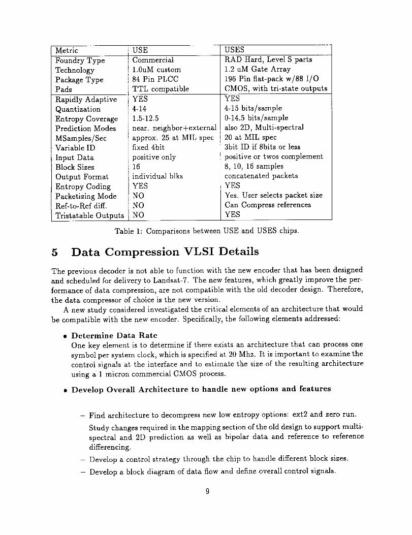
Metric USE USESFoundry TypeTechnologyPackageTypePadsltapidly AdaptiveQuantizationEntropy CoveragePrediction ModesMSamples/Sec
Commercial1.0uMcustom84 Pin PLCCTTL compatibleYES
4-14
1.5-12.5
near. neighbor+external
approx. 25 at MIL spec
RAD Hard, Level S parts
1.2 uM Gate Array
196 Pin fiat-pack w/88 I/O
CMOS, with tri-state outputs
YES
4-15 bits/sample
0-14.5 bits/sample
also 2D, Multi-spectral
20 at MIL spec
Variable ID
Input DataBlock Sizes
Output Format
Entropy Coding
Packetizing Mode
Ref-to-Ref diff.
Tristatable Outputs
fixed 4bit
positive only16
individual blks
YES
NO
NO
NO
3bit ID if 8bits or less
positive or twos complement
8, 10, 16 samples
concatenated packets
YES
Yes. User selects packet size
Can Compress references
YES
Table 1: Comparisons between USE and USES chips.
5 Data Compression VLSI Details
The previous decoder is not able to function with the new encoder that has been designed
and scheduled for delivery to Landsat-7. The new features, which greatly improve the per-
formance of data compression, are not compatible with the old decoder design. Therefore,
the data compressor of choice is the new version.
A new study considered investigated the critical elements of an architecture that would
be compatible with the new encoder. Specifically, the following elements addressed:
• Determine Data Rate
One key element is to determine if there exists an architecture that can process one
symbol per system clock, which is specified at 20 Mhz. It is important to examine the
control signals at the interface and to estimate the size of the resulting architecture
using a 1 micron commercial CMOS process.
• Develop Overall Architecture to handle new options and features
- Find architecture to decompress new low entropy options: ext2 and zero run.
- Study changes required in the mapping section of the old design to support multi-
spectral and 2D prediction as well as bipolar data and reference to reference
differencing.
- Develop a control strategy through the chip to handle different block sizes.
- Develop a block diagram of data flow and define overall control signals.
9
• Develop a Specification
- The end product of this study is a proposed specification that could be imple-
mented and meets NASA's needs, especially in terms of:
• Interface requirements.
• Compatibility with flight encoder.
6 Delivery of VLSI to the Government
There has always been a problem in producing chips that have been developed under NASA
sponsorship after the initial delivery has been made. Accordingly, the University of New
Mexico solved this problem in a unique manner. A not-for-profit company, named ICs, was
established to accomplish the following:
• Market and sell VLSI to the Government and Government contractors
• Provide technical support to systems designers in the use and function of the VLSI
• Provide Class B and Class S quality screening for flight programs
• Migrate technology to advanced CMOS processes and new foundries.
At this writing ICs has provided VLSI to the following organizations and programs:
10
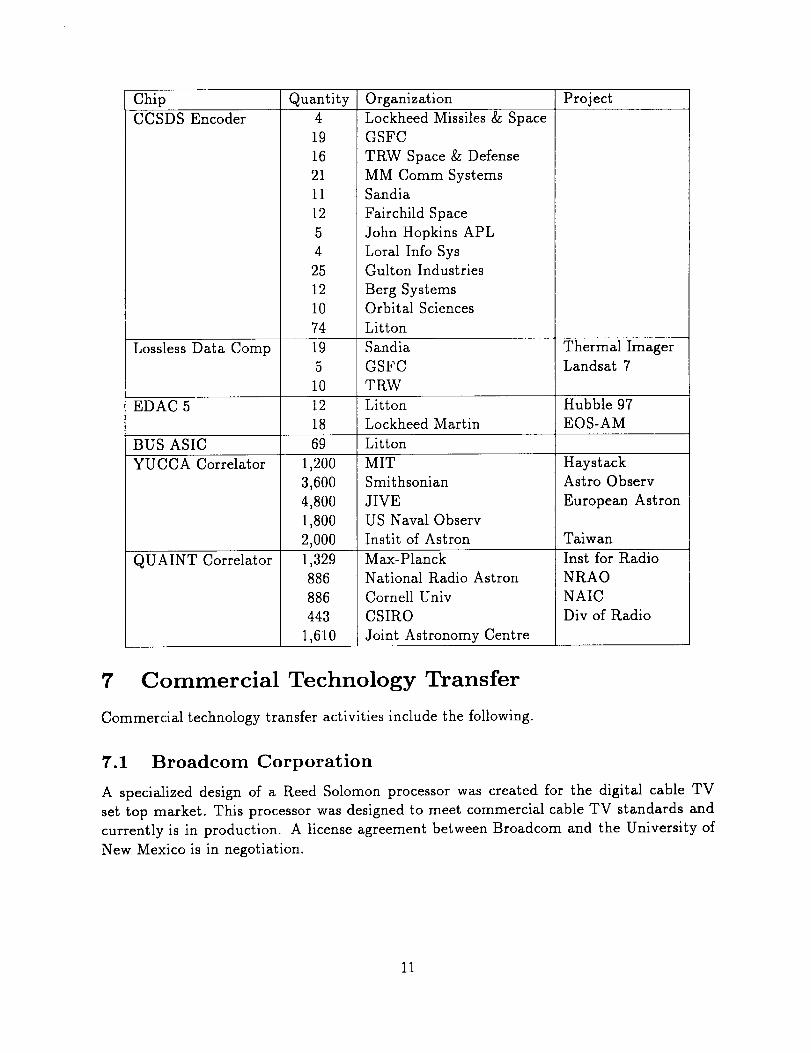
Chip Quantity Organization ProjectCCSDSEncoder 4
19162111125425121074
LockheedMissiles& SpaceGSFCTRW Space& DefenseMM Comm SystemsSandiaFairchild SpaceJohn HopkinsAPLLoral Info Sys
Gulton Industries
Berg SystemsOrbital Sciences
Litton
Lossless Data Comp 19 Sandia Thermal Imager
5 GSFC Landsat 7
10 TRW
EDAC 5 12 Litton Hubble 97
18 Lockheed Martin EOS-AM
BUS ASIC 69 Litton
YUCCA Correlator 1,200
3,600
4,800
1,800
2,000
1,329
886
886
443
1,610
QUAINT Correlator
MIT
Smithsonian
JIVE
US Naval Observ
Instit of Astron
Max-Planck
National Radio Astron
Cornell Univ
CSIRO
Joint Astronomy Centre
Haystack
Astro Observ
European Astron
Taiwan
Inst for Radio
NRAO
NAIC
Div of Radio
7 Commercial Technology Transfer
Commercial technology transfer activities include the following.
7.1 Broadcom Corporation
A specialized design of a Reed Solomon processor was created for the digital cable TV
set top market. This processor was designed to meet commercial cable TV standards and
currently is in production. A license agreement between Broadcom and the University of
New Mexico is in negotiation.
11
7.2 1773 Transceiver
The 1773 optical Transceiver processor was completed this year and a license agreement
established with Honeywell. Honeywell will market this processor nation wide.
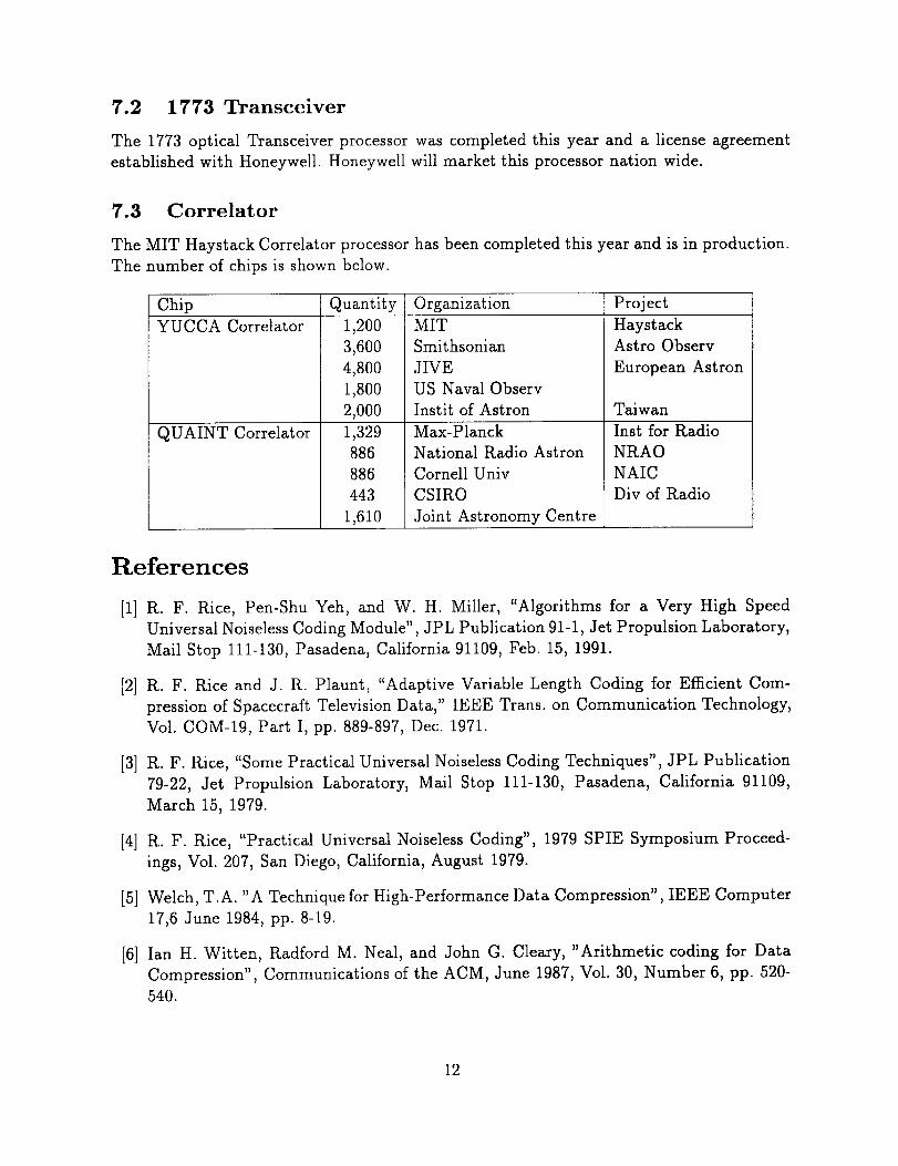
7.3 Correlator
The MIT Haystack Corrclator processor has been completed this year and is in production.
The number of chips is shown below.
Chip Quantity Organization Project
YUCCA Correlator
QUAINT Correlator
1,200
3,600
4,800
1,800
2,000
1,329886
886
443
1,610
MIT
Smithsonian
JIVE
US Naval Observ
Instit of Astron
Max-Planck
National Radio Astron
Cornell Univ
CSIRO
Joint Astronomy Centre
HaystackAstro Observ
European Astron
Tai w an
Inst for Radio
NRAO
NAIC
Div of Radio
References
[1] R. F. Rice, Pen-Shu Yeh, and W. H. Miller, "Algorithms for a Very High Speed
Universal Noiseless Coding Module", JPL Publication 91-1, Jet Propulsion Laboratory,
Mail Stop 111-130, Pasadena, California 91109, Feb. 15, 1991.
[2] R. F. Rice and J. R. Plaunt, "Adaptive Variable Length Coding for Efficient Com-
pression of Spacecraft Television Data," IEEE Trans. on Communication Technology,
Vol. COM-19, Part I, pp. 889-897, Dec. 1971.
[3] R. F. Rice, "Some Practical Universal Noiseless Coding Techniques", JPL Publication
79-22, Jet Propulsion Laboratory, Mail Stop 111-130, Pasadena, California 91109,
March 15, 1979.
[4] R. F. Rice, "Practical Universal Noiseless Coding", 1979 SPIE Symposium Proceed-
ings, Vol. 207, San Diego, California, August 1979.
[5] Welch, T.A. "A Technique for High-Performance Data Compression", IEEE Computer
17,6 June 1984, pp. 8-19.
[6] Ian H. Witten, Radford M. Neal, and John G. Cleary, "Arithmetic coding for Data
Compression", Communications of the ACM, June 1987, Vol. 30, Number 6, pp. 520-
540.
12
[7] J. Venbrux, G. Zweigle,J. Gambles,D. Wiseman,W. Miller andP.Yeh, "An Adaptive,LosslessData CompressionAlgorithm andVLSI Implementations",NASA Symposiumon VLSI Design,pp 1.3.1-1.3.15,November1993.
[8] Pen-ShuYeh, R. F. Rice,and W. H. Miller, "On the Optimality of CodeOptions fora Universal NoiselessCoder", JPL Publication 91-2,Jet Propulsion Laboratory, MailStop 111-130,Pasadena,California 91109,Feb. 15,1991.
[9] Data CompressionProducts AHA3370 and AHA3371,AdvancedHardware Architec-tures, NE 2365Hoplins Court, Pullman, WA 99163.
13