Embed Size (px)
Citation preview
55:041 Electronic Circuits The University of Iowa Fall 2010
1
Final Exam
Name: ____________________________ Score ___________
Max: 135
Question 1 (1, unless otherwise noted)
1. An engineer measures the (step response) rise time of an amplifier as .
Estimate the 3 dB bandwidth of the amplifier.
Answer:
2. In the current mirrors below, neglect the base currents. What is ?
Answer:
3. An engineer designs a class-AB amplifier to deliver 2 W (sinusoidal) signal power
to an resistive load. Ignoring saturation in the output BJTs, what is the required
peak-to-peak voltage swing across the load? (2 points)
Answer
, so that , so that
55:041 Electronic Circuits The University of Iowa Fall 2010
2
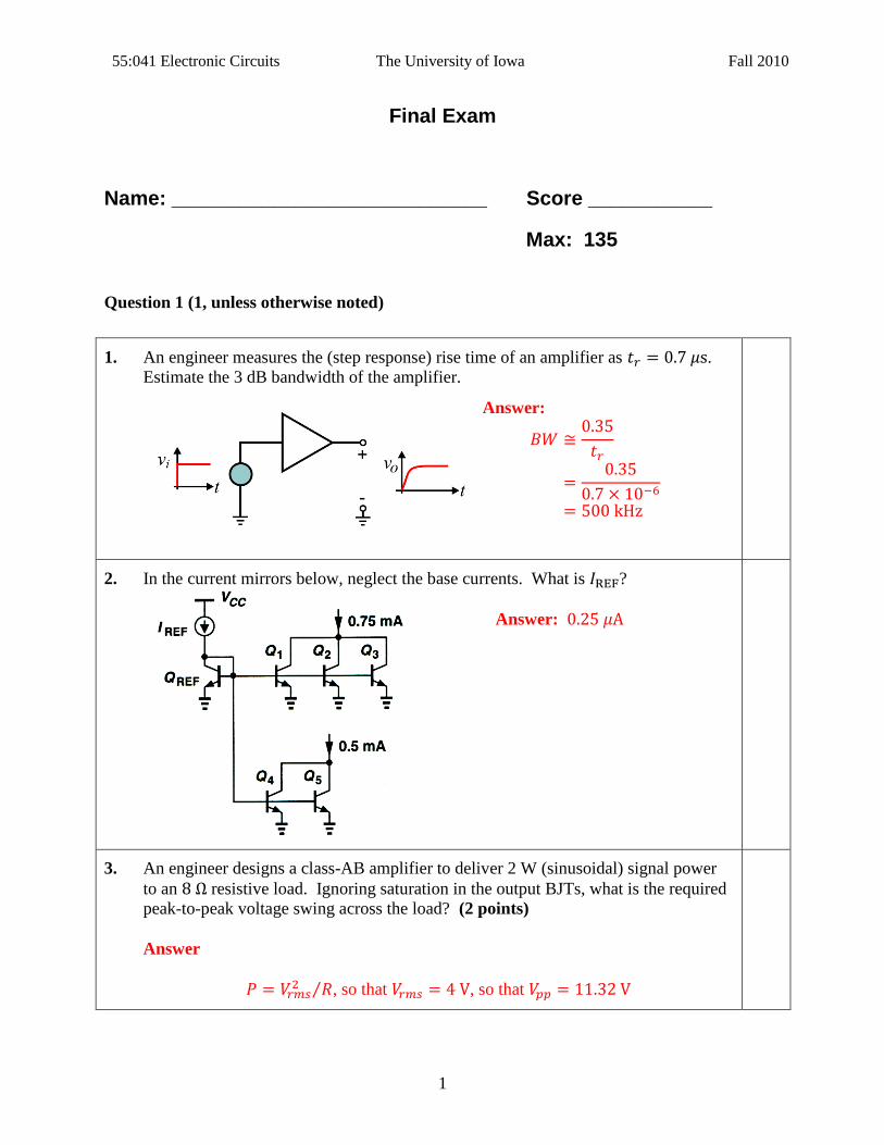
4. Many BJT datasheets do not list explicitly, but list an equivalent h-parameter
instead. What is this parameter?
Answer:
5. A MOSFET is biased such that and . If changes
with 1 mV, by how much does the drain current change?
Answer
6. Estimate the voltage gain of the following amplifier.
Answer:
7. For the following circuit, what is the numerical value for the two-port y-parameter
? (3 points)
Answer:
Short port 1, then apply a voltage and determine the current that flows into port 1,
and apply the definition above. Then
55:041 Electronic Circuits The University of Iowa Fall 2010
3
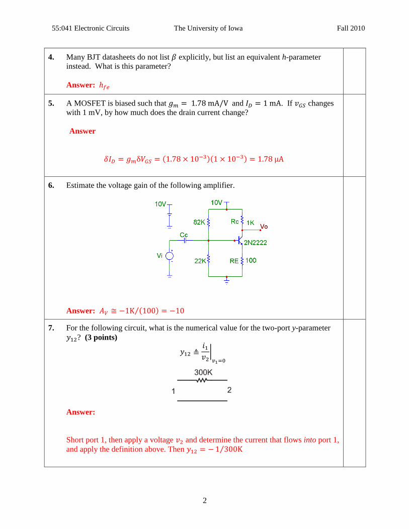
8. What type of negative feedback (series-shunt, series-series,…) is used in the
following amplifier?
Answer: Shunt-shunt
9. The output voltage of a three-terminal voltage regulator is 5 V @ 5 mA load, and
4.96 V @ 1.5 A load. What is the regulator’s output resistance?
Answer:
10. The output voltage of a three-terminal voltage regulator is 5 V @ 5 mA load, and
4.96 V @ 1.5 A load. What is the regulator’s load regulation?
Answer
11. Classify the following filter as active/passive and lowpass/high-pass, etc.
Answer: Active high-pass

55:041 Electronic Circuits The University of Iowa Fall 2010
4
12. Classify the following filter as active/passive and lowpass/high-pass, etc.
Answer: Active low-pass
13. Classify the following filter as active/passive and lowpass/high-pass, etc.
Answer: Active high-pass
14. Classify the following filter as active/passive and lowpass/high-pass, etc.
Answer: Active low-pass
15. Classify the following filter as active/passive and lowpass/high-pass, etc. (2 points)
Answer: Active bandpass
55:041 Electronic Circuits The University of Iowa Fall 2010
5
16. An amplifier with gain of 200 has a 10% variation in gain over a certain frequency
range. Using negative feedback, what value of should one use to reduce the gain
variation to 1%? (3 points)
Answer. The improvement factor we want from the negative feedback is
. Therefore,
17. An amplifier has gain of 100,000, and a 20% variation in gain over a certain
temperature range. Negative feedback is used to reduce the gain to 10. What is the
variation in gain with temperature of the feedback amplifier? (3 points)
Answer. The gain is reduced by . The
temperature variations are reduced by the same factor, so the feedback amplifier’s
gain varies by
18. An op-amp has an open-loop gain of 120 dB and an input resistance of . An
engineer wants to use negative feedback to obtain an amplifier with input resistance
of 5 . What is the gain (in dB) of the feedback amplifier? (2 points)
Answer. Negative feedback increases the resistance by (or 40 dB) and reduces the gain by the same factor, so the feedback amplifier’s
gain is 80 dB.
19. An single-pole op-amp has an open-loop low-frequency gain of and an
open loop, 3-dB frequency of 4 Hz. If an inverting amplifier with closed-loop low-
frequency gain of uses this op-amp, determine the closed-loop
bandwidth. (2 points)
Answer. The gain-bandwidth product is . The bandwidth of the closed-
loop amplifier is then is .
55:041 Electronic Circuits The University of Iowa Fall 2010
6
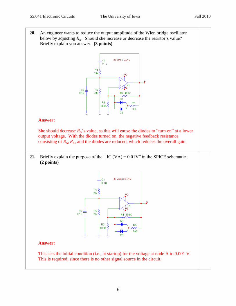
20. An engineer wants to reduce the output amplitude of the Wien bridge oscillator
below by adjusting . Should she increase or decrease the resistor’s value?
Briefly explain you answer. (3 points)
Answer:
She should decrease ’s value, as this will cause the diodes to “turn on” at a lower
output voltage. With the diodes turned on, the negative feedback resistance
consisting of , and the diodes are reduced, which reduces the overall gain.
21. Briefly explain the purpose of the “.IC (VA) = 0.01V” in the SPICE schematic .
(2 points)
Answer:
This sets the initial condition (i.e., at startup) for the voltage at node A to 0.001 V.
This is required, since there is no other signal source in the circuit.
55:041 Electronic Circuits The University of Iowa Fall 2010
7
Question 2 The open-loop low-frequency gain of an op-amp is 100 dB. At a frequency of
the magnitude of the open-loop gain is 38 dB. The op-amp has a dominant-pole
open-loop response. Determine the frequency of the dominant pole and the unity-gain
bandwidth. (5 points)
Solution
Open-loop dominant pole response implies constant GBP, which is
The dominant-pole frequency is
The unity-gain bandwidth is the same as GBP.
Question 3 With inputs , and , a difference amplifier has output
With inputs , the output is . Determine the
CMRR, expressed in dB. (5 points)
Solution
The differential input voltage is , and the differential-mode gain
is
With the common-mode voltage gain is
The common-mode rejection ratio is
Expressed in dB

55:041 Electronic Circuits The University of Iowa Fall 2010
8
Question 4 For the circuit below , and Further,
and and a dc analysis show that (10 points)
What is the lower 3 dB corner frequency? Hint: use BJT scaling and determine Then use
the time-constant technique.
Solution
Using BJT impedance scaling
The time constant associated with the coupling capacitor is
The lower corner frequency is then
55:041 Electronic Circuits The University of Iowa Fall 2010
9
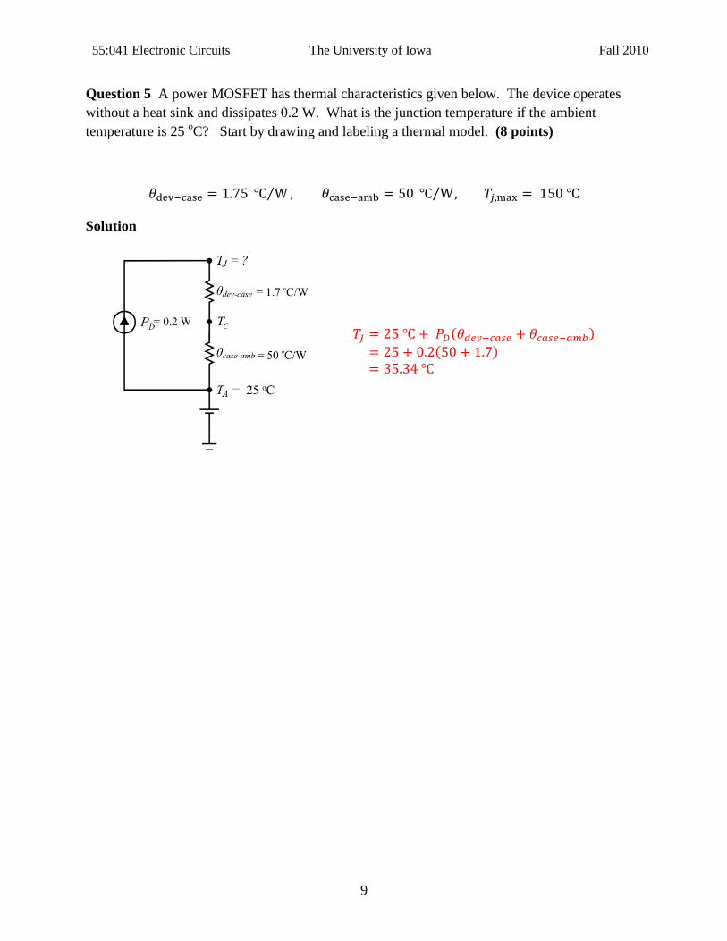
Question 5 A power MOSFET has thermal characteristics given below. The device operates
without a heat sink and dissipates 0.2 W. What is the junction temperature if the ambient
temperature is 25 oC? Start by drawing and labeling a thermal model. (8 points)
Solution
55:041 Electronic Circuits The University of Iowa Fall 2010
10
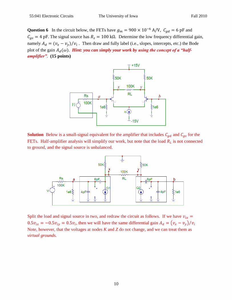
Question 6 In the circuit below, the FETs have , and
The signal source has . Determine the low frequency differential gain,
namely . Then draw and fully label (i.e., slopes, intercepts, etc.) the Bode
plot of the gain . Hint: you can simply your work by using the concept of a “half-
amplifier”. (15 points)
Solution Below is a small-signal equivalent for the amplifier that includes and for the
FETs. Half-amplifier analysis will simplify our work, but note that the load is not connected
to ground, and the signal source is unbalanced.
Split the load and signal source in two, and redraw the circuit as follows. If we have
, then we will have the same differential gain
Note, however, that the voltages at nodes K and Z do not change, and we can treat them as
virtual grounds.

55:041 Electronic Circuits The University of Iowa Fall 2010
11
Page Intentionally Left Blank
The resulting half amplifier circuit is then
Similarly, , so that . This is an
inverting amplifier and the 6 pF capacitor between the drain and gate will experience the Miller
multiplication. The Miller gain is the gain from node a to x, or .
Now
The calculated values match those obtained via SPICE
55:041 Electronic Circuits The University of Iowa Fall 2010
12
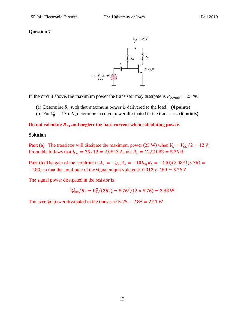
Question 7
In the circuit above, the maximum power the transistor may dissipate is .
(a) Determine RL such that maximum power is delivered to the load. (4 points)
(b) For , determine average power dissipated in the transistor. (6 points)
Do not calculate , and neglect the base current when calculating power.
Solution
Part (a) The transistor will dissipate the maximum power (25 W) when .
From this follows that and .
Part (b) The gain of the amplifier is
, so that the amplitude of the signal output voltage is .
The signal power dissipated in the resistor is
The average power dissipated in the transistor is
55:041 Electronic Circuits The University of Iowa Fall 2010
13
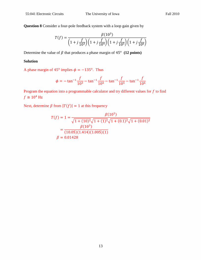
Question 8 Consider a four-pole feedback system with a loop gain given by
Determine the value of that produces a phase margin of (12 points)
Solution
A phase margin of implies . Thus
Program the equation into a programmable calculator and try different values for to find
Next, determine from at this frequency
55:041 Electronic Circuits The University of Iowa Fall 2010
14
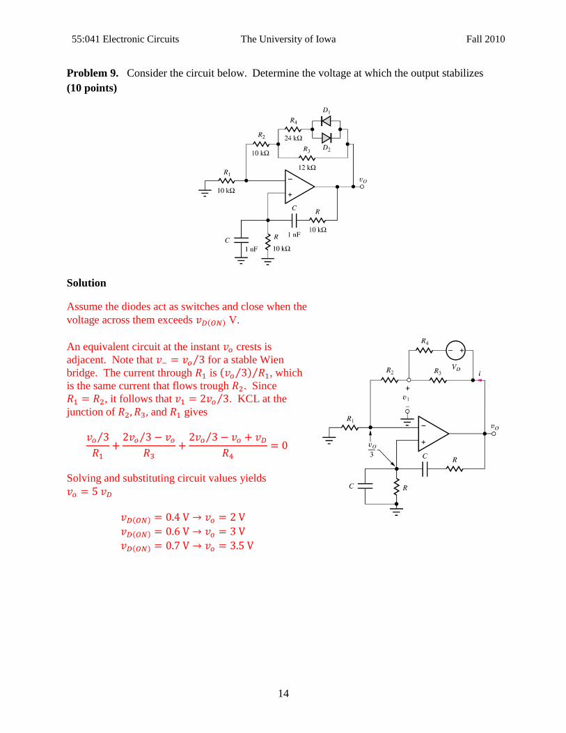
Problem 9. Consider the circuit below. Determine the voltage at which the output stabilizes
(10 points)
Solution
Assume the diodes act as switches and close when the
voltage across them exceeds V.
An equivalent circuit at the instant crests is
adjacent. Note that for a stable Wien
bridge. The current through is , which
is the same current that flows trough . Since
, it follows that . KCL at the
junction of and gives
Solving and substituting circuit values yields
55:041 Electronic Circuits The University of Iowa Fall 2010
15
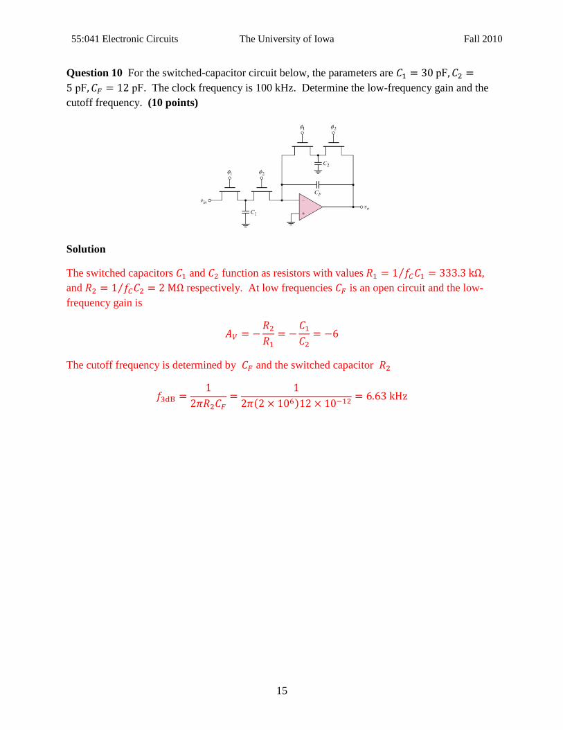
Question 10 For the switched-capacitor circuit below, the parameters are p
p p . The clock frequency is 100 kHz. Determine the low-frequency gain and the
cutoff frequency. (10 points)
Solution
The switched capacitors and function as resistors with values ,
and respectively. At low frequencies is an open circuit and the low-
frequency gain is
The cutoff frequency is determined by and the switched capacitor
55:041 Electronic Circuits The University of Iowa Fall 2010
16
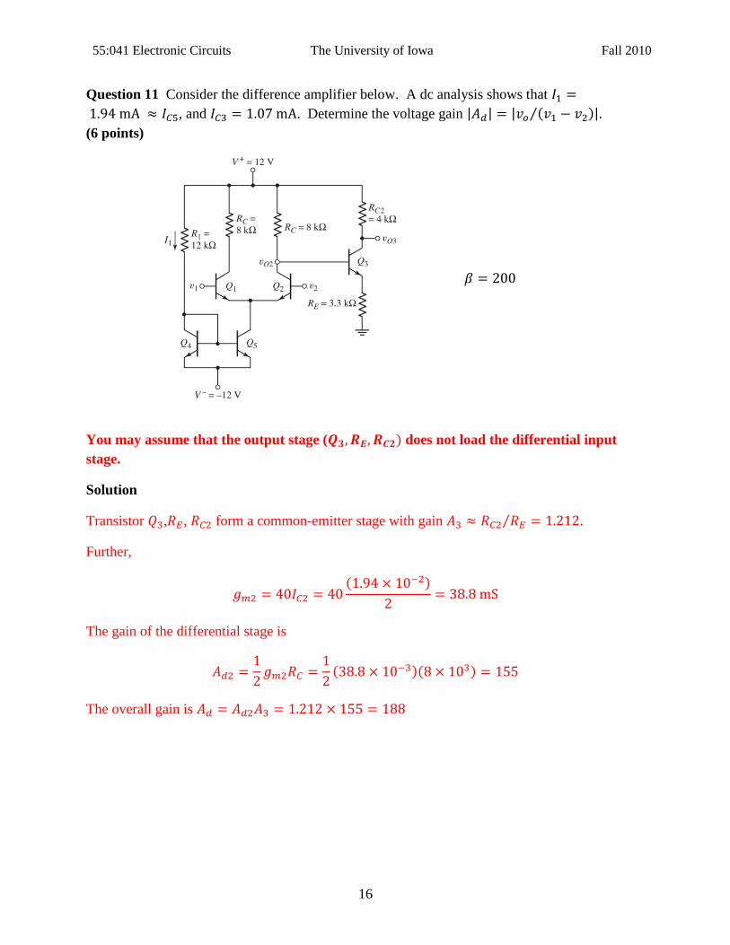
Question 11 Consider the difference amplifier below. A dc analysis shows that
, and . Determine the voltage gain .
(6 points)
You may assume that the output stage ( does not load the differential input
stage.
Solution
Transistor , , form a common-emitter stage with gain .
Further,
The gain of the differential stage is
The overall gain is
55:041 Electronic Circuits The University of Iowa Fall 2010
17
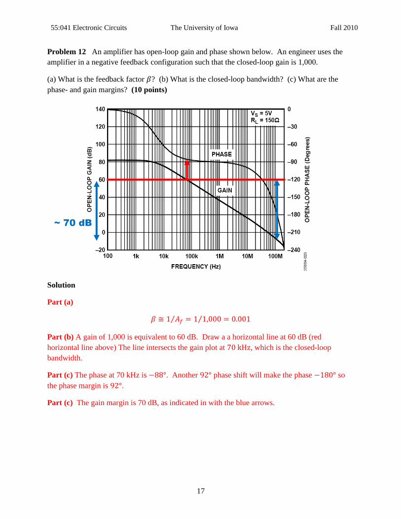
Problem 12 An amplifier has open-loop gain and phase shown below. An engineer uses the
amplifier in a negative feedback configuration such that the closed-loop gain is 1,000.
(a) What is the feedback factor ? (b) What is the closed-loop bandwidth? (c) What are the
phase- and gain margins? (10 points)
Solution
Part (a)
Part (b) A gain of 1,000 is equivalent to 60 dB. Draw a a horizontal line at 60 dB (red
horizontal line above) The line intersects the gain plot at , which is the closed-loop
bandwidth.
Part (c) The phase at 70 kHz is . Another phase shift will make the phase so
the phase margin is
Part (c) The gain margin is 70 dB, as indicated in with the blue arrows.
~ 70 dB