Embed Size (px)
Citation preview

IOP PUBLISHING NANOTECHNOLOGY
Nanotechnology 20 (2009) 000000 (8pp) UNCORRECTED PROOF
Fabrication of plasmonic Au nanovoidtrench arrays by guided self-assemblyXiaoli V Li1, R M Cole2, C A Milhano3, P N Bartlett3, B F Soares2,J J Baumberg2 and C H de Groot1
1 School of Electronics and Computer Science, University of Southampton,Southampton SO17 1BJ, UK2 Department of Physics, University of Cambridge, J J Thomson Avenue,Cambridge CB3 0HE, UK3 School of Chemistry, University of Southampton, Southampton SO17 1BJ, UK
E-mail: [email protected] and [email protected]
Received 27 March 2009, in final form 5 May 2009PublishedOnline at stacks.iop.org/Nano/20/000000
(Ed: )
Ascii/Word/NAN/
nano313708/PAP
Printed 26/5/2009
Spelling UK
Issue noTotal pagesFirst pageLast pageFile nameDate reqArtnum
Cover dateAbstractMetallic nanoscale voids can support both localized and propagating plasmons and formplasmonic crystals. However, constructing 1D arrays is crucial for producing plasmoniccircuits. In this paper we report the first experimental evidence of plasmons in templated lineararrays of self-assembled structures. Single and multilayer arrays of gold voids have beenfabricated through self-assembly of sub-micron polystyrene spheres in V-shaped trenches inQ.1
silicon, followed by selective area electrodeposition. Angle-dependent dispersioncharacteristics reveal the existence of localized plasmons.
(Some figures in this article are in colour only in the electronic version)Q.2
1. Introduction
Plasmonic devices rely on the interaction of light with freecharges, and are key to optical sensing and waveguiding [1].High quality three-dimensional colloidal sphere arrays haveattracted attention due to their potential to act as a templatefor the fabrication of 3D photonic crystals for waveguidestructures, optical filters or switches [2]. In previouswork [3, 4], we have shown that spherical nanoscale voids inmetal possess different, and potentially more useful, plasmonicmodes than nanoscale metal particles. In particular, it hasbeen shown that spherical nanoscale voids, fabricated usinga substrate of hexagonal close-packed self-assembled spheresas a template, support both propagating and localized plasmonmodes, as shown in figure 1 [3, 4]. In 2D nanovoid arraysthe incident energy spreads out rapidly and pulses dispersein many directions, while on the other hand in linear chainsof nanovoids propagation can be very low loss and non-dispersive. This compares to nanoparticle plasmon chainswhich quench propagation after only one or two interparticlehops. Only by making linear arrays of such nanovoid structuresis it possible to guide plasmons in specific geometric directionsand fabricate plasmon waveguides which will enable on-chipoptical communication. However, previously it has not beenpossible to control the direction of plasmon propagation.
Patterned or guided assembly of a few micron or sub-micron sized particles has recently attracted a lot of attention,and assembly of various kinds of particles in trenches and holeshas been demonstrated. This method allows the formation ofshapes of a size which is at least an order of magnitude smallerthan that of the pattern made by (photo-) lithography or othermeans. Cheng et al succeeded in regular assembly of blockco-polymers of 50 nm period [5, 6] which is particularly usefulfor high density storage [7]. However, for optical interactions,particle sizes of the order of visible light wavelengths arerequired. Ozin et al have shown both theoretically andexperimentally the optical absorption spectra of self-assembledpolystyrene spheres on patterned silicon [8, 9] as haveSun et al on polycarbonate substrates [10]. Whisperinggallery modes have been detected in one-dimensional arraysof self-assembled spheres by Hara et al [11] although inthis experiment the polymer spheres had to be selectedspectroscopically to reduce the sphere to sphere size variation.
Mono-dispersed spherical colloids can self-assemble intoone, two, or three-dimensional lattices [12–14] by varioustypes of driving forces, such as gravity, convection, spin-coating or electrostatics [15–18]. On flat substrates, spheresself-assemble due to capillary forces into hexagonal close-packed mono- or multi-layers, as a maximum packing density
0957-4484/09/000000+08$30.00 © 2009 IOP Publishing Ltd Printed in the UK1

Nanotechnology 20 (2009) 000000 X V Li et al
Figure 1. (a) Schematic of surface plasmons (blue, in colour on-line)and localized plasmons (red) existing on gold nanoscale voidsurfaces. θ is the angle of incidence with respect to the normal, and� the angle with respect to the hexagonal lattice director. ((b), (c))Typical experimental angle-dependent plasmon dispersions, withabsorption from 0% (dark blue) to 80% (red/white), for (b) apropagating surface plasmon (black lines indicate theoreticaldispersion modelled using the Bragg scattering equation), and (c) alocalized plasmon (dashed lines indicate expected plasmon energy).Existence of the different plasmons depends on the thickness of theAu. See [3] for details.Q.A
is the energetically favourable structure. However, onpatterned substrates, the main packing force is the surfaceinteractions between the spheres and the walls of the template.Therefore the packing structure of spheres on a patternedsubstrate is primarily directed by local physical constraints, asshown in [19–28].
In this paper, we use self-assembly of polystyrenespheres on patterned substrates to create a template forthe electrodeposition of Au nanoscale void arrays. Sphereassembly in flat bottomed trenches has previously beendemonstrated by Conway et al [29] and Woodcock [30],however here we use V-shaped trenches and show how theobserved ordered crystal stacking is uniquely controlled in thisconfiguration. The diameter of the polystyrene spheres andhence the size of Au voids is around 500 nm, which allows us toprobe both self-assembly formation and plasmon modes withvisible light. The quality and fidelity of both the self-assemblyof polystyrene spheres as well as the electrodeposition of Aunanovoids is such that we have been able to detect the existenceof localized plasmons by optical means. The energy of theplasmons is shown to depend on the dielectric constant at the
Au interface. This is the first experimental evidence of linearplasmon arrays in templated self-assembled structures.
2. Experimental section
The templates were assembled using mono-disperse poly-styrene polystyrene spheres (Duke Scientific Corporation)supplied as a 1 wt% solution in water (manufacturer’scertified mean diameter of 499 nm ± 5 nm, coefficient ofvariation in diameter 1.3%). Before use the suspensionswere homogenized by successive, gentle inversions for 5min followed by a sonication for 15 s. All solvents andchemicals were of reagent quality and were used withoutfurther purification. The commercial cyanide free gold platingsolution (Tech. Gold 25, containing 7.07 g dm−3 gold) wasobtained from Technic Inc. (Cranston, RI, USA). Fumingnitric acid and dimethylformamide (DMF) was obtained fromAldrich. 20:1 buffered hydrogen fluoride (BHF) was obtainedfrom Rockwood. All solutions were freshly prepared usingreagent-grade water (18 M� cm) from a Cartridge Elgadeioniser system.
The pre-patterned Si substrates were prepared from n-type (100)-polished Si substrate wafers with 0.01–0.02 � cmresistivity. The process flow for the samples is outlined infigure 2. A 250 nm layer of SiO2 was thermally grown. Aphotolithography pattern was then transferred onto the wafersurface and the oxide was dry etched down to the underlyingSi, creating linear trench arrays of 400 μm length, with widthsW varying from 500 to 1700 nm with a step size of 100 nmand separation between the strips of either 500 or 1000 nm.To obtain V-shaped trenches, Si wet etching by potassiumhydroxide (KOH) was carried out, (figure 2(b)). Thisintrinsically anisotropic etching technique utilizes a relativeetch rate for (111)/(100) Si planes of about 350 [18]. Thereforeorientation-dependent etching of (100)-polished Si through thepatterned SiO2 mask creates precise V-shaped trenches, with anangle of 70.6◦ between two (111)-planes. Wafers are cleanedusing a two-step RCA clean, with an aqueous mixture ofhydrogen peroxide and ammonium hydroxide and a mixtureof hydrogen peroxide and hydrochloric acid. Prior to thedeposition of spheres, a 20:1 BHF dip is used to etch thenative oxide layer off the exposed Si. In order to assemble thecolloidal spheres on the patterned Si wafer, a clean uncoatedmicroscope slide was attached to the wafer forming a water-tight cell. A layer of Parafilm was used to prevent the leakagefrom the cell, and a hatch was left to allow the injectionof the colloidal solution. The cell was clamped verticallyand the solution allowed to evaporate naturally over 10 h,enabling assembly of the spheres in the trenches, as shown infigure 2(c). Prior to electrodeposition, a second 20:1 BHF dip(6 s) was necessary to remove the native oxide and leave theSi surface H-terminated. Electrodeposition of gold was thenperformed at ambient temperature using a conventional three-electrode configuration controlled by an Autolab PGSTAT12.The sample was the working electrode with a platinum gauzecounter electrode and a saturated calomel reference electrode(SCE). A pulse of −1.1 V versus SCE was applied for0.2 s to nucleate electrodeposition. The gold nanoscalevoids were gradually electrodeposited under potentiostatic
2
Nanotechnology 20 (2009) 000000 X V Li et al
Figure 2. ((a)–(d)) Process flow and schematic view for templated self-assembly of inverse sphere metal arrays in V-shaped trenches: (a) SiO2
dry etch by hydrofluoric acid through a lithographically patterned photo-resist layer (not shown) (b) Si anisotropic etch by potassiumhydroxide (c) self-assembly of polystyrene spheres by solvent evaporation (d) Au electrodeposition on Si through the polystyrene template.(e) The water preferentially wets the SiO2 thus forcing the spheres along the trench into contact. (f) Sequential SEM images of 600 nmcolloidal spheres assembled in a 3D lattice inside a tapered trench of length 75 μm, width from 2500 nm (top left) to 560 nm (bottom right).
conditions at −0.7 V versus SCE. Since SiO2 is an insulator,electrodeposition only takes place on the Si trench walls, asshown in figure 2(d). After electrodeposition, the sample wasplaced into dimethylformamide (DMF) solvent and washed inan ultrasonic tank for 2 h in order to dissolve the polystyrenesphere template. The morphology and nanostructure of boththe colloidal templates and gold nanoscale void arrays werecharacterized using scanning electron microscopy (SEM, LEO1455VP SEM). A fibre-coupled spectrometer (Ocean Optics,spectral range 400–1700 nm, resolution 1 nm) placed in thefocal plane of the reflection image was used to obtain thespectral response from the selected area (approximate diameter50 μm).
3. Results and discussion
3.1. Templated self-assembly of colloidal spheres
Polystyrene spheres assembled in the V-shaped trenches, arefirst characterized by SEM. Spheres with diameter Dn =500 nm, can be seen assembled three-dimensionally in a trenchof nominal width Wn = 1800 nm in figure 3(a). From the rightmost trench in the SEM image in which the layer below the toplayer is revealed, it is clear that the spheres assemble in a facecentred cubic (fcc) lattice with the (001) plane in the plane ofthe wafer and the (110) direction parallel to the trench lengthand the Si (110) direction. The number of spheres observedin the top layer perpendicular to the trench corresponds to thenumber of dense packed planes of the colloidal crystal withinthe V-shaped trenches. The angle in the shown fcc stackingof the spheres with its (111) plane parallel to the crystal Si(111) planes means that the fcc polystyrene sphere lattice has
an identical angle to the horizontal plane as the Si. The (111)packing of the sphere lattice forms hence parallel to the trenchangled sidewalls, maximizing the number of spheres touchingthe Si wall. Hence fcc is the closest-packed arrangement ina KOH etch Si trench when the trench width is commensuratewith the sphere size. This is in contrast to flat bottom structuresin which the hexagonal lattice is instead favoured for a singlelayer [29, 30], which will build up to a fcc lattice with the(111) plane in the plane of the wafer as shown in [31]. Theorientation of the assembled structure is hence predictablycontrolled by the geometry of the trench.
The most dense ordered packing is expected for acommensurate trench size with the width W of the trench equalto W = nD + A with n the integer identical to the numberof layers, and A an offset due to spheres not being able toaccess the bottom apex of the V-grooved trench. However,as nothing would stop the spheres partially assembling in theanisotropically etched SiO2 above the Si, the effective offsetcan be essentially zero. Although there is some fluctuation,experimentally for sphere diameter D = 500 nm, the four-layer structure assembles most repeatably in a trench ofmeasured width Wn = 2130 nm, the three-layer structurein Wn = 1580 nm, the two layer in Wn = 1020 nm, andthe one layer in Wn = 470 nm as shown in figure 3. Therelation between experimental width and sphere diameter forcommensurate structures hence fits closely the relation We =nD with the data suggesting that for wider structures it needs tobe slightly larger than the commensurate size to accommodateboth the variation in sphere size (1.3%) and aligned movementas the fcc phase forms.
It is also worth noting that the polystyrene spheres do notassemble on SiO2 surfaces in the vicinity of the Si trenches. On
3

Nanotechnology 20 (2009) 000000 X V Li et al
Figure 3. SEM images of 500 nm polystyrene sphere arrays that were assembled into trenches by controlled evaporation of water. In (a) with1580 nm trench width, the first sub-layer is exposed in the bottom right-hand side revealing the fcc lattice, with schematic (b) top view and (c)cross-sectional view of the self-assembled lattice. Trenches of width (d) 470 nm and (e) 1020 nm support single and double layers of spheresrespectively.
un-patterned planar Si or SiO2 surfaces, polystyrene spheresassemble into a close-packed array driven by strong lateralcapillary forces [32], which develop at the meniscus betweenthe solution and substrate and between adjacent spheres. Incontrast, on the patterned Si wafer, the mechanism of self-assembly is altered as competing surface energies play a role.The buffered hydrogen fluoride dip used on the Si surfacebefore self-assembly leaves the surface H-terminated, andthus hydrophobic. Hence it is expected that the SiO2 hasa smaller contact angle and higher surface energy than theSi surface. The liquid better wets the SiO2 thus retractingfrom the Si trenches first and is only retained in the vicinityof the polystyrene spheres which are lifted up to the rimedge and brought into contact with the previously depositedspheres (see figure 2(e)). The combination of maximizingelectrostatic attraction between the spheres and the Si trenchsidewalls, and the capillary forces developed by the differentwetting of trench and rim appears to guarantee dense orderedpacking in this system. This close-packed geometry is criticalfor the subsequent fabrication of Au nanovoid linear arrayssince the touching spheres produce eventually interconnectingholes between the voids that control the hopping of localizedplasmons along the chain [3].
3.2. Optical characteristics of patterned and self-assembledstructures
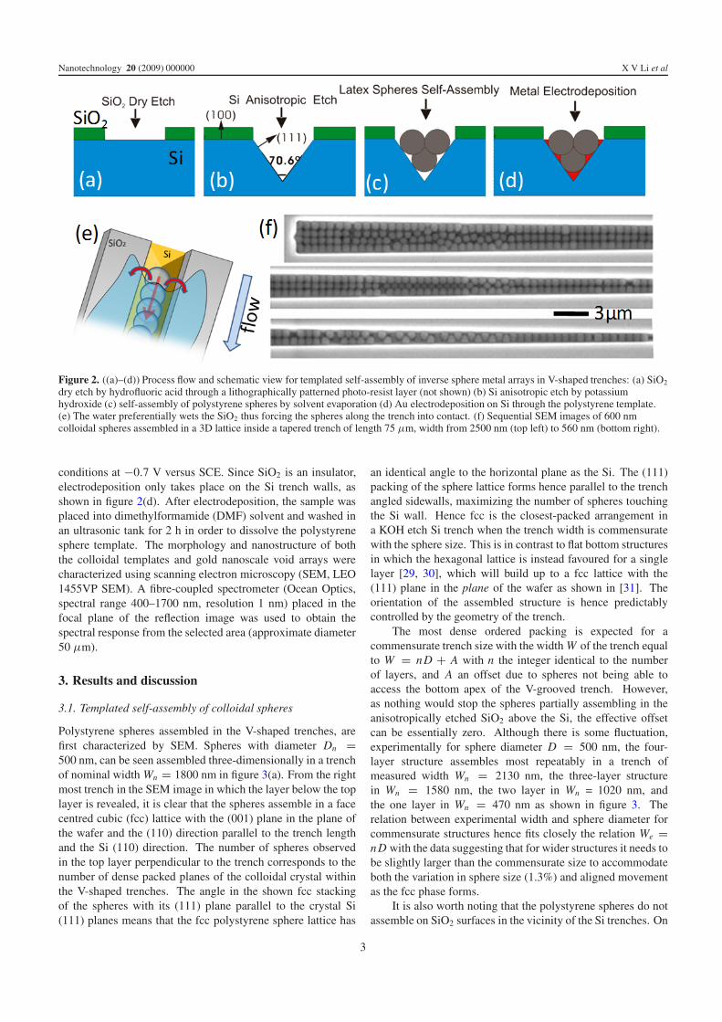
Un-patterned Si wafers appear dark grey in dark fieldmicroscopy. The intrinsic colouration of the wafers seen in
figure 4 is due to optical diffraction from the periodic micropatterning of the surface. Unfilled trenches of nominal widthsfrom 500 to 1200 nm were imaged in dark field configuration,as shown in figure 4(a). In dark field imaging, light impinges athigher angles (10◦) and only scattered (i.e. diffracted) light atnormal incidence is collected by the objective, as in figure 4(c).A simple calculation of the peak diffracted wavelengths asa function of trench pitch shows excellent agreement withthe microscope image colours (figure 4(d)), providing a rapidmethod to verify the trench pitch and substrate uniformity atprecise locations. Figure 4(b) shows an equivalent substratewith spheres assembled into the trenches. The spheresmodify the local refractive index, tuning the effective pitchof the trenches, and hence tuning their colour. From theuniformity of trench array colour, the sphere packing densitycan be measured, as observed in figure 4(e) for samples ofincreasing sphere concentration in the trenches. Well-orderedsamples with good adhesion to the patterned substrate appearopalescent.
3.3. Gold electrodeposition through colloidal sphere template
After self-assembly, the 3D lattices are used as templates tofabricate Au nanoscale void arrays on Si by electrodeposition.A pulse of −1.1 V versus SCE for 0.2 s is used to form a layerof uniform Au nucleation as with Si as the electrodepositioninterface, instantaneous uniform nucleation is crucial to obtaina continuous gold film [33]. A potential of −0.7 V versusSCE was selected to allow the gradual electrodeposition of Au
4
Nanotechnology 20 (2009) 000000 X V Li et al
Figure 4. Dark field microscope images of 250 μm-long trench arrays with width varying step-wise from 600 to 1200 nm and fixed spacingbetween trenches of 500 nm, either (a) empty or (b) filled with self-assembled polystyrene sphere. Colour changes across each filled trencharray are due to changes in the local refractive index, which is directly related to the sphere packing density and uniformity. (c) Schematic oflight collection by microscope in dark field configuration. (d) Calculated diffracted wavelengths for the three lowest diffraction orders as afunction of trench width, with appropriate corresponding colours (on-line). (e) Dark field microscope images of trench arrays with increasingdensity of polystyrene spheres. Sphere packing density can be inferred from each image.
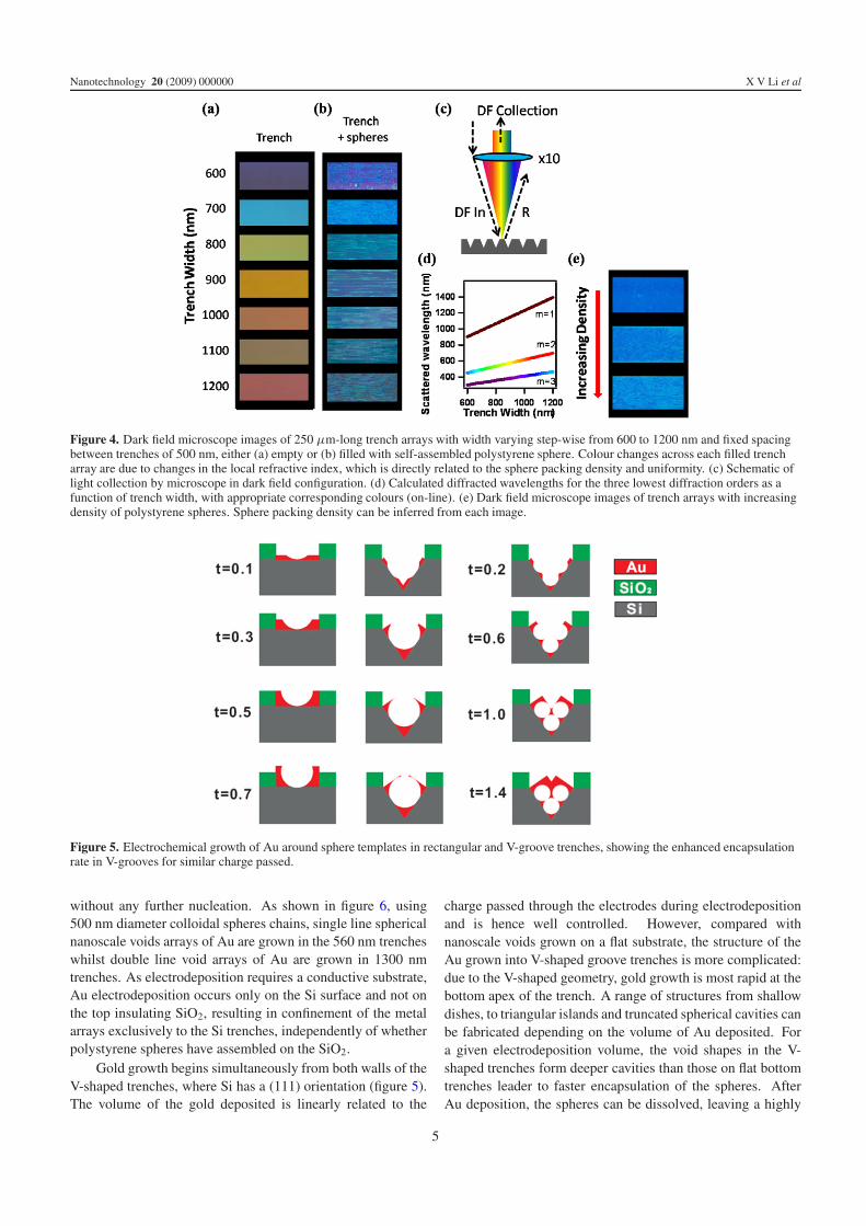
Figure 5. Electrochemical growth of Au around sphere templates in rectangular and V-groove trenches, showing the enhanced encapsulationrate in V-grooves for similar charge passed.
without any further nucleation. As shown in figure 6, using500 nm diameter colloidal spheres chains, single line sphericalnanoscale voids arrays of Au are grown in the 560 nm trencheswhilst double line void arrays of Au are grown in 1300 nmtrenches. As electrodeposition requires a conductive substrate,Au electrodeposition occurs only on the Si surface and not onthe top insulating SiO2, resulting in confinement of the metalarrays exclusively to the Si trenches, independently of whetherpolystyrene spheres have assembled on the SiO2.
Gold growth begins simultaneously from both walls of theV-shaped trenches, where Si has a (111) orientation (figure 5).The volume of the gold deposited is linearly related to the
charge passed through the electrodes during electrodepositionand is hence well controlled. However, compared withnanoscale voids grown on a flat substrate, the structure of theAu grown into V-shaped groove trenches is more complicated:due to the V-shaped geometry, gold growth is most rapid at thebottom apex of the trench. A range of structures from shallowdishes, to triangular islands and truncated spherical cavities canbe fabricated depending on the volume of Au deposited. Fora given electrodeposition volume, the void shapes in the V-shaped trenches form deeper cavities than those on flat bottomtrenches leader to faster encapsulation of the spheres. AfterAu deposition, the spheres can be dissolved, leaving a highly
5

Nanotechnology 20 (2009) 000000 X V Li et al
Figure 6. SEM images of 500 nm nanoscale void arrays. The voids are grown by Au electrodeposition using the assembled polystyrene linearsphere arrays as templates. ((a), (b)) Single nanovoid arrays in trenches of width 560 nm with (a) polystyrene spheres present or (b) dissolved.((c), (d)) Double nanovoid arrays in trenches of width 1300 nm with polystyrene spheres (c) present or (d) dissolved. The insets show theview of the structure tilted at a 45◦ angle.
stable Au nanovoid morphology. Such isolated plasmon array3D structures have not previously been fabricated, and are hardto conceive of using alternative routes.
3.4. Optical characteristics of gold nanovoids
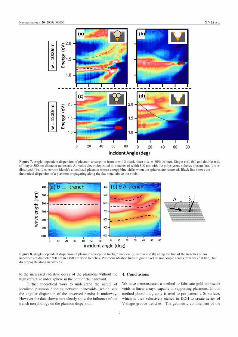
Angle-dependent optical characterization of these structuresreveals a rich variety of optical and plasmonic modes,which are strongly dependent on the lattice structure and Authickness. Angular-dispersion measurements can reveal thenature of the observed plasmon modes, as depicted in figure 1.Optical reflectivity measurements for two different samples areshown in figure 7. The samples were illuminated with visiblelight from 400 to 1700 nm, and incident scan angles from 0◦ to80◦. The thickness ratio t/D is 0.5 for the upper sphere in eachstructure, corresponding to a semi-truncated spherical cavity.First we identify weak but highly dispersive (i.e. stronglyangle dependent) modes which correspond to propagatingplasmon modes on the top of the Au (solid line in figure 7(a)),where the plasmon frequency depends on the incident photonwavevector. The dispersion of these modes corresponds toplasmons propagating along the length of the trenches. Thesemodes disappear when the sample is oriented so the incidentlight is oriented not along, but across the nanovoid trencharrays, as such plasmons can no longer propagate (figure 8(a)).We note also that the plasmonic absorption in our linearnanovoid array devices is less pronounced than on un-patterned2D array substrates, due to the reduced nanovoid density.
The data also reveals highly localized modes (dashedlines), which due to their confined spatial extent, have awell defined plasmon frequency across a wider angular range.These modes are characterized by a flat dispersion, and arepredominant in high aspect ratio nanoscale void structures.Hopping of localized plasmons between neighbouring spherescan be identified from the presence of ‘nearly’ localizedplasmons with mixed Bragg–Mie dispersion (figure 8(b))—these plasmon bands weakly disperse and show anti-crossingbehaviour where they meet. Whereas light incident on a 2Dhexagonal nanoscale void array can couple to plasmon modesat any incident azimuthal angle to the crystal lattice, in thetrench structures only light incident parallel to the trenches willcouple strongly to plasmon modes, with only weak couplingto localized plasmons by light incident perpendicular to thetrenches. This highlights the crucial role of the trenches inguiding and confining the propagating plasmons.
Both the localized modes and dispersive modes are betterdefined with the colloidal spheres left in place (providing ahigh refractive core confining the plasmons better). It canalso be seen that the localized plasmon present in the single-layer structure (figure 7(a), red arrow) shifts to higher energywhen the spheres are removed (figure 7(b)). This is a directconsequence of the lower dielectric constant of the air ascompared to the colloidal spheres, as described in detail in [34].In addition, the plasmon linewidths are broader when thespheres are removed (more than doubling the linewidth) due
6
Nanotechnology 20 (2009) 000000 X V Li et al
Figure 7. Angle-dependent dispersion of plasmon absorption from α = 0% (dark blue) to α = 80% (white). Single-((a), (b)) and double-((c),(d)) layer 500 nm diameter nanoscale Au voids electrodeposited in trenches of width 840 nm with the polystyrene spheres present ((a), (c)) ordissolved ((b), (d)). Arrows identify a localized plasmon whose energy blue-shifts when the spheres are removed. Black line shows thetheoretical dispersion of a plasmon propagating along the flat metal above the voids.
Figure 8. Angle-dependent dispersion of plasmon absorption for light incident (a) across and (b) along the line of the trenches of Aunanovoids of diameter 500 nm in 1490 nm wide trenches. Plasmons (dashed lines to guide eye) do not couple across trenches (flat line), butdo propagate along nanovoids.
to the increased radiative decay of the plasmons without thehigh refractive index sphere in the core of the nanovoid.
Further theoretical work to understand the nature oflocalized plasmon hopping between nanovoids (which setsthe angular dispersion of the observed bands) is underway.However the data shown here clearly show the influence of thetrench morphology on the plasmon dispersion.
4. Conclusions
We have demonstrated a method to fabricate gold nanoscalevoids in linear arrays, capable of supporting plasmons. In thismethod photolithography is used to pre-pattern a Si surface,which is then selectively etched in KOH to create series ofV-shape groove trenches. The geometric confinement of the
7
Nanotechnology 20 (2009) 000000 X V Li et al
trenches together with electrostatic interactions and surfacetension guides the (110) fcc assembly of the spheres onthis patterned Si surface. Zero-defect arrays were found toassemble along the entire length of some trenches for 500 nmdiameter spheres, allowing characterization with visible light.The long-range well-ordered sphere strip arrays are used astemplates to form gold nanoscale void linear arrays by acarefully-developed electrodeposition process optimized forthis architecture. By varying the film thickness, void shapesranging from shallow dishes to encapsulated voids werefabricated. The gold nanovoid linear arrays are of high qualitywith respect to lateral symmetry and allow the detection ofanisotropic plasmonic dispersion. Further understanding ofthe different plasmon modes will aid research into slow-lightand active waveguides and potentially allow on-chip opticalcommunication through nanovoid plasmon chains.
References
[1] Lal S, Link S and Halas N J 2007 Nat. Photon. 1 641[2] Wiley B J, Im S H, Li Z, McLellan J, Siekkinen A and
Xia Y 2006 J. Phys. Chem. B 110 15666[3] Kelf T A, Sugawara Y, Cole R M, Baumberg J J,
Abdelsalam M E, Cintra S, Mahajan S, Russell A E andBartlett P N 2006 Phys. Rev. B 74 245415
[4] Cole R M, Baumberg J J, Garcia de Abajo F J, Mahajan S,Abdelsalam M and Bartlett P N 2007 Nano Lett. 7 2094
[5] Cheng J Y, Ross C A, Thomas E L, Smith H I and JuliusVancso G 2003 Adv. Mater. 15 1599
[6] Cheng J Y, Mayes A M and Ross C A 2001 Nat. Mater. 3 823[7] Park S, Lee D H, Xu J, Kim B, Hong S W, Jeong U, Xu T and
Russell T P 2009 Science 323 1030[8] Ozin G A and Yang S M 2001 Adv. Funct. Mater. 11 95[9] Yang S M, Mı́guez H and Ozin G A Adv. Funct. Mater. 12 425Q.3
[10] Sun J, Li Y, Dong H, Zhan P, Tang C, Zhu M and Wang Z 2008Adv. Mater. 20 123
[11] Hara Y, Mukaiyama T, Takeda K andKuwata-Gonokami M 2005 Phys. Rev. Lett. 94 203905
[12] Bae C, Shin H and Moon J 2007 Chem. Mater. 19 1531[13] Ye J, Zentel R, Arpiainen S, Ahopelto J, Jonsson F,
Romanov S G and SotomayorTorres M C 2006 Langmuir22 7378
[14] Nagayama K 1996 Colloids Surf. A 109 363[15] Donselaar L N, Philipse A P and Suurmond J 1997 Langmuir
13 6018[16] Denkov N D, Velev O D, Kralchevsky P A, Ivanov I B,
Yoshimura H and Nagayama K 1992 Langmuir 8 3183[17] Hulteen J C and van Duyne R P 1995 J. Vac. Sci. Technol. A
13 1553[18] Kalsin A M, Fialkowski M, Paszewski M, Smoukov S K,
Bishop K J M and Grzybowski B A 2006 Science 312 420[19] van Blaaderen A, Ruel R and Wiltzius P 1997 Nature 385 321[20] Kiziroglou M E, Li X, Gonzalez D C, de Groot C H,
Zhukov A A, de Groot P A J and Bartlett P N 2006 J. Appl.Phys. 100 113720
[21] Ozin G A and Yang S M 2001 Adv. Funct. Mater. 11 95[22] Yang S M and Ozin G A 2000 Chem. Commun. 2507[23] Yin Y D, Lu Y, Gates B and Xia Y 2001 J. Am. Chem. Soc.
123 8718[24] Yin Y D, Li Z Y and Xia Y 2003 Langmuir 19 622[25] Xia Y, Yin Y D, Lu Y and McLennan J 2003 Adv. Funct.
Mater. 13 907[26] WU S, Tang T and Tseng W J 2008 J. Mater. Sci. 43 6453[27] Ye Y H, Badilescu S and Truong V 2001 Appl. Phys. Lett.
79 872[28] Hur J and Won Y 2008 Soft Matter 4 1261[29] Conway J H and Sloane N J A 1988 Sphere Packings, Lattices
and Groups (New York: Springer)[30] Woodcock L V 1997 Nature 385 141–3[31] Zhukov A A, Goncharov A V, de Groot P A J, Bartlett P N and
Ghanem M A 2003 J. Appl. Phys. 93 7322[32] Kralchevsky P A and Denkov N D 2001 Curr. Opin. Colloid
Interface Sci. 6 383[33] Kiziroglou M E, Zhukov A A, Li X, Gonzalez D C,
de Groot P A J, Bartlett P N and de Groot C H 2006 SolidState Commun. 140 508
[34] Cole R M, Sugawara Y, Baumberg J J, Mahajan S,Abdelsalam M and Bartlett P N 2006 Phys. Rev. Lett.97 137401
8

Queries for IOP paper 313708
Journal: NanoAuthor: X V Li et alShort title: Fabrication of plasmonic Au nanovoid trencharrays by guided self-assembly
Page 1
Query 1:Author: ‘through guided’ or ‘by guided’ better in title?
Query 2:Author: Please be aware that the colour figures in this
article will only appear in colour in the Web version. If yourequire colour in the printed journal and have not previouslyarranged it, please contact the Production Editor now.
Page 2
Query A:Author: If figures 1, 4 and 7 are not to be printed in colour
please provide alternatives for the colours mentioned in thecaptions.
Page 8
Query 3:-Author: [9]: Please provide year.
Reference linking to the original articles
References with a volume and page number in blue have a clickable linkto the original article created from data deposited by its publisher atCrossRef. Any anomalously unlinked references should be checked foraccuracy. Pale purple is used for links to e-prints at ArXiv.