Embed Size (px)
Citation preview

Embedded Flash Technologies: Enabler for Automotive µCs & Smartcards
Workshop on Innovative Memory Technologies
MINATEC, Grenoble, 2012-06-21
Dr. Robert Strenz, Infineon Technologies Dresden GmbH

Workshop on Innovative Memory Technologies, MINATEC, Grenoble, 2012-06-21
Page 2 Copyright © Infineon Technologies 2012. All rights reserved.
Infineon eNVM Design & Technology Team
Special thanks to
Robert Allinger, Thomas Kern, Klaus Knobloch,
Wolfram Langheinrich, Patrick Leteinturier,
Robert Wiesner and Georg Tempel

Workshop on Innovative Memory Technologies, MINATEC, Grenoble, 2012-06-21
Set date Page 3 Copyright © Infineon Technologies 2012. All rights reserved.
Technology Requirements
Cell Concepts
Market & Applications
Outlook
Workshop on Innovative Memory Technologies, MINATEC, Grenoble, 2012-06-21
Set date Page 4 Copyright © Infineon Technologies 2012. All rights reserved.
Technology Requirements
Cell Concepts
Market & Applications
Outlook

Workshop on Innovative Memory Technologies, MINATEC, Grenoble, 2012-06-21
Page 5 Copyright © Infineon Technologies 2012. All rights reserved.
Embedded Flash ICs
IC with on-chip embedded flash
memory
Mostly used for µC products
Typically …
… compatible with bulk CMOS
technology
… embedded with SRAM, ROM &
Mixed Signal IP Example: Infineon µC TC1784 , 90nm
(180 MHz, 2.5 MByte Flash)

Workshop on Innovative Memory Technologies, MINATEC, Grenoble, 2012-06-21
Page 6 Copyright © Infineon Technologies 2012. All rights reserved.
Why Embedded ?
Cost of Flash-integration (SoC) vs. 2-chip solution (SiP)*
¬ Cost ratio SoC vs. SiP is key & depends on many parameters:
SiP technology Die size NVM/Logic area ratio Number of required connections vs. chip geometry Interface speed requirements Voltage compatibility of frontend technologies to combine Production volume vs. cost of embedded NVM dev’t
¬ For a broadband eFlash IDM today it’s very difficult to find SiP solutions that serve the whole product portfolio
¬ SiP is and will be an addition to SoC, not a replacement
Performance: direct code execution from embedded flash
Security (Smartcards)
Application-inherent for some products
(e.g. Flash-based FPGAs) *see also (1) A. Maurelli et al.

Workshop on Innovative Memory Technologies, MINATEC, Grenoble, 2012-06-21
Page 7 Copyright © Infineon Technologies 2012. All rights reserved.
Embedded Flash Applications
Automotive µCs ~4B$ Market Smartcards ~ 2B$ Market
Consumer & Industrial Applications
Wide variety of applications, no reliable market data available

Workshop on Innovative Memory Technologies, MINATEC, Grenoble, 2012-06-21
Page 8 Copyright © Infineon Technologies 2012. All rights reserved.
Automotive µC & Smartcard Market
Data source:
iSuppli Q1 2012 update

Workshop on Innovative Memory Technologies, MINATEC, Grenoble, 2012-06-21
Page 9 Copyright © Infineon Technologies 2012. All rights reserved.
Technology Requirements
Cell Concepts
Market & Applications
Outlook

Workshop on Innovative Memory Technologies, MINATEC, Grenoble, 2012-06-21
Page 10 Copyright © Infineon Technologies 2012. All rights reserved.
Key Technology Requirements for ATV µCs
Product Technology
Direct code execution,
access times < 10…20ns
High reading current of code
memory (typically >20µA)
Frequent updates of data
memory (e.g. start/stop
system)
Data-Memory w/ high
endurance & retention lifetime
(500k cycles + full operational
lifetime)
Under hood applications
(e.g. engine & gear shift
control)
Broad Temperature Range
(Tj = -40°C … 175°C)
Safety critical applications Ultra-low fail rates < 1ppm

Workshop on Innovative Memory Technologies, MINATEC, Grenoble, 2012-06-21
Page 11 Copyright © Infineon Technologies 2012. All rights reserved.
Key Technology Requirements for Smartcards
Product Technology
Fast prog & erase w/ small
data granularity (e.g. GSM
cards)
Short erase time (< 5ms)
w/ page or smaller granularity
Frequent data update (e.g.
change of encryption keys for
Pay-TV)
High write/erase endurance
(>200k cycles)
Good retention after cycling
(M2M products)
Typical application profile:
5y retention after 100k cycling

Workshop on Innovative Memory Technologies, MINATEC, Grenoble, 2012-06-21
Page 12 Copyright © Infineon Technologies 2012. All rights reserved.
Technology Requirements
Cell Concepts
Market & Applications
Outlook

Workshop on Innovative Memory Technologies, MINATEC, Grenoble, 2012-06-21
Page 13 Copyright © Infineon Technologies 2012. All rights reserved.
Mainstream eFlash Concepts
1T-NOR Splitgate 2T-NOR
1) 2)
P/E (1) CHE / FN
(2) FN / FN
(1) SSI / FN
(2) SSI / HHI
FN/FN
Storage Floating Gate (1) Floating Gate
(2) ONO
Floating Gate
Area 10 - 30 F2 20 - 30 F2 25 - 100 F2
Main
Players
(1) FSL, ST, TI
(2) Infineon
(1) SST-licensees
(2) Renesas
NXP, Samsung
(3) C. Peters et al. (4) F. Ito et al., (5) X. Liu et al. (6) D. Dormans et al.,
(7) Y.K. Lee et al.

Workshop on Innovative Memory Technologies, MINATEC, Grenoble, 2012-06-21
Page 14 Copyright © Infineon Technologies 2012. All rights reserved.
Area Tradeoff: Bitcell vs. Module Overhead
Bitcell Area (arb.u.)
1T-NOR (e.g. CHE/FN, FN/FN)
2T-NOR (FN/FN)
Splitgate-NOR (e.g. SSI-FN, SSI-HHE)
HV-EEPROM (pos. voltage FN/FN) N
VM
IP
Overh
ead
Are
a
(arb
.u.)
Favorable for higher
memory densities
Favorable for smaller
memory densities

Workshop on Innovative Memory Technologies, MINATEC, Grenoble, 2012-06-21
Page 15 Copyright © Infineon Technologies 2012. All rights reserved.
Except Area: Pros & Cons
1T-NOR Splitgate 2T-NOR
1) 2)
P/E High prog thruput
No overerase
High Iread
Low power
consumption
No overerase
Storage Overerase
handling required
Tradeoff erase
speed vs. read
speed
Some concepts
need triple poly
process complexity
Workshop on Innovative Memory Technologies, MINATEC, Grenoble, 2012-06-21
Page 16 Copyright © Infineon Technologies 2012. All rights reserved.
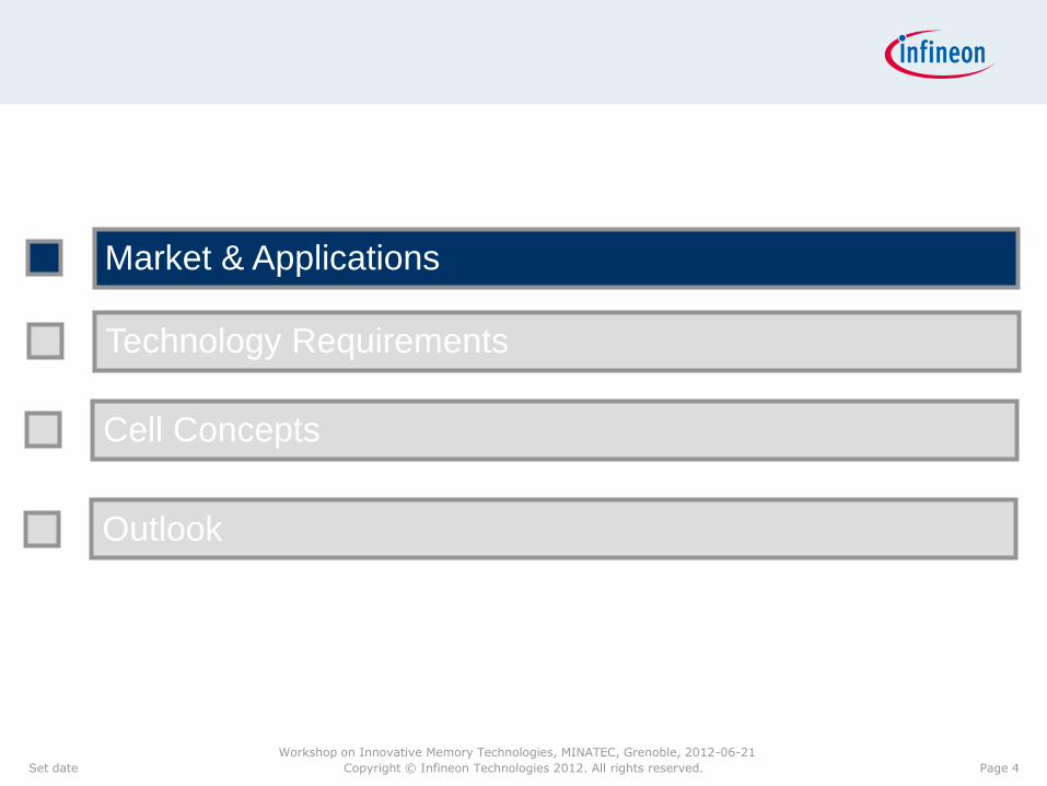
FG-based Cells: TOX scaling has stopped because of SILC (Low-T Retention)
As TOX scaling has stopped, there is no further HV scaling most cell design rules get limited by device physics bitcell area scaling is slowing down
Data from Infineon’s 90nm generation

Workshop on Innovative Memory Technologies, MINATEC, Grenoble, 2012-06-21
Page 17 Copyright © Infineon Technologies 2012. All rights reserved.
FG-based Cells: Flash T-Budget vs. SRAM Functionality
Stronger Flash sidewall oxidation improves endurance, but impacts SRAM yield
Tradeoff between flash reliability and SRAM yield becomes more and more critical with advanced CMOS nodes
Data Source: IFX 90nm generation
Workshop on Innovative Memory Technologies, MINATEC, Grenoble, 2012-06-21
Page 18 Copyright © Infineon Technologies 2012. All rights reserved.
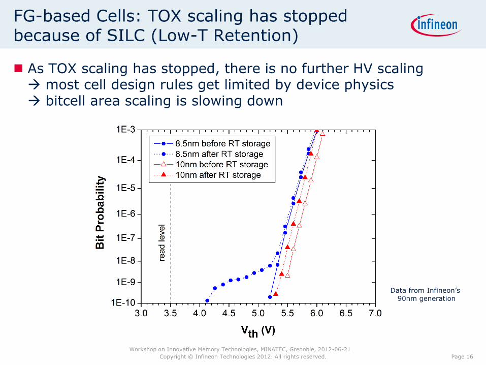
Retention After Cycling: SONOS vs. FG-based
Intrinsic retention after cycling performance of SONOS cells is worse
than FG based cells
For high endurance applications (e.g. M2M applications) design
solutions are necessary (e.g. differential sensing)
(9) F. Maugain et al. (ST) (8) Kumar et al.
(10)
Workshop on Innovative Memory Technologies, MINATEC, Grenoble, 2012-06-21
Page 19 Copyright © Infineon Technologies 2012. All rights reserved.
There is no optimum eFlash concept.
It’s all about finding the best compromise for your product
portfolio.

Workshop on Innovative Memory Technologies, MINATEC, Grenoble, 2012-06-21
Page 20 Copyright © Infineon Technologies 2012. All rights reserved.
Technology Requirements
Cell Concepts
Market & Applications
Outlook

Workshop on Innovative Memory Technologies, MINATEC, Grenoble, 2012-06-21
Page 21 Copyright © Infineon Technologies 2012. All rights reserved.
Embedded NVM Size & ATV µC System Perforamnce
ATV µC trend for more embedded memory
& system speed will go on

Workshop on Innovative Memory Technologies, MINATEC, Grenoble, 2012-06-21
Page 22 Copyright © Infineon Technologies 2012. All rights reserved.
Embedded Flash New Node Introduction History
Leading edge eFlash volume production today is 90nm. 65nm is just about to be introduced by major players.
New eFlash node introduction speed slows down w.r.t. CMOS

Workshop on Innovative Memory Technologies, MINATEC, Grenoble, 2012-06-21
Page 23 Copyright © Infineon Technologies 2012. All rights reserved.
Embedded Flash Scaling Outlook
Scaling of classical eFlash bitcells slows down in terms of F2 Strong increase of wafer cost < 4x nm will lead to chip cost
saturation New flash integration challenges for HKMG 28nm
Economic pressure on embedded emerging concepts will increase tremendously
published bitcell areas:

Workshop on Innovative Memory Technologies, MINATEC, Grenoble, 2012-06-21
Page 24 Copyright © Infineon Technologies 2012. All rights reserved.
Embedded Flash Emerging Concepts: Pros & Cons
PCRAM STT-MRAM RRAM
Main Pros
w.r.t.
Classical
Cells
Scalability
Cost
(Slightly) faster
write/erase
Scalability
Cost,
Fast write/erase (partial SRAM replacement)
Scalability
Cost
(Slightly) faster
write/erase
Status Standalone NOR
products available
R&D phase for STT-
MRAM (Field switching products only)
R&D phase,
no products yet
Challenges Retention currently
limited to ~ 80°C
(GST225)
Extrinsic reliability
modes
Thermal stability vs.
cell size
No significant array
data published yet
No array data
published yet
Limited retention
demonstrated so
far (~ 100°C/10y)
Main
Players
Micron (Numonyx/ST)
Samsung, Hynix
Samsung/Grandis, Renesas,
Toshiba/Hynix, Everspin, Crocus
Adesto/Altis, Samsung,
Macronix, Toshiba
eFlash players are underlined
see e.g. IEDM 2011 (10) A. Lacaita et al. (11) W.J. Gallagher et al. (12) R. Waser et al.

Workshop on Innovative Memory Technologies, MINATEC, Grenoble, 2012-06-21
Page 25 Copyright © Infineon Technologies 2012. All rights reserved.
PCRAM RRAM STT-MRAM
So far none of emerging concepts have demonstrated
reliability & manufacturing potential to cover
significant part of eFlash market

Workshop on Innovative Memory Technologies, MINATEC, Grenoble, 2012-06-21
Page 26 Copyright © Infineon Technologies 2012. All rights reserved.
Renesas Roadmap: Against All Odds ?
Renesas being one of STT-MRAM technology leaders, announced 1st STT-MRAM product for 65nm node years ago
Today Renesas …
… skipped 65nm node
… announced 40nm sampling w/ MONOS for 2nd half of 2012
… announced 28nm node still to be MONOS
(13) Y. Yano, ISSCC 2012

Workshop on Innovative Memory Technologies, MINATEC, Grenoble, 2012-06-21
Page 27 Copyright © Infineon Technologies 2012. All rights reserved.
While the Emerging Race is On: Infineon’s Path for Extending Classical Bitcell’s Lifetime is HS3P
Infineon 65nm cell concept HS3P
(Hot Source Triple Poly)
SSI program, FN channel erase
0.13 µm2 bitcell area
Competitive flash module areas:
Multi-market 512kByte module
with 0.91µm2
SoP expected 2H-2012
See also (14) D. Shum et al.

Workshop on Innovative Memory Technologies, MINATEC, Grenoble, 2012-06-21
Page 28 Copyright © Infineon Technologies 2012. All rights reserved.
Thank You !

Workshop on Innovative Memory Technologies, MINATEC, Grenoble, 2012-06-21
Page 29 Copyright © Infineon Technologies 2012. All rights reserved.
References
1) Maurelli, A., Belot, D., Campardo, G., “SoC and SiP, the Yin and Yang of the Tao for the New Electronic Era”, Proc. Of the IEEE, Vol.97, pp 9-17
2) Data source: iSuppli, Q1 2012 update
3) Christian Peters, Holger Sedlak, Gerd Dirscherl, Michael Bollu, Andreas Schlaffer and Stefanie Thierold, “A 130nm high-density embedded EEPROM as Universal Memory for code and data storage based on a 1T FN/FN Flash cell”, Proc. NVSMW (2004), pp. 55,56
4) F. Ito et al., “A Novel MNOS Technology Using Gate Hole Injection in Erase Operation for Embedded Non-Volatile Memory Applications”, Symposium on VLSI Technology (2004), pp. 80-81
5) Xian Liu, Viktor Markov, Alexander Kotov, Tho Ngoc Dang, Amitay Levi, “Endurance Characteristics of SuperFlash® Memory”, Proc. ICSICT (2006)
6) Do Dormans, Jochen Garbe, Dick Boter, Han Dijkstra and Rob Verhaar,” High-density low-voltage byte-erasable EEPROM memory based on a 2T-FNFN Flash cell”, Proc. NVSMW 2003
7) Y.K. Lee et al., “2T-FN eNVM with 90 nm Logic process for Smart Card, Proc. NVSMW/ICMTD 2008
8) Kumar et al., “Endurance and Retention Characteristics of SONOS EEPROMs Operated Using BTBT Induced Hot Hole Erase”, IRPS 2006
9) F. Maugain et al., “90nm e-Page Flash for Machine to Machine Applications”, Workshop on Innovative Memory Technologies, Leti, Grenoble 2011
10) A. Lacaita, “The phase change run to nonvolatile storage at the nanoscale”, IEDM 2011 Short Course on Advanced Memory Technology
11) W.J. Gallagher, „Emerging Magnetic Memory Technologies“, IEDM 2011 Short Course on Advanced Memory Technology
12) R. Waser, “Redox-based Resisitive Switching Memories – the Mystery of Nanoionic Processes”, IEDM 2011 Short Course on Advanced Memory Technology
13) Y. Yano, “Take the Expressway to Go Greener”, ISSCC 2012
14) D. Shum et al., “Highly Reliable Flash Memory with Self-aligned Split-gate Cell Embedded into High Performance 65nm CMOS for Automotive & Smartcard Applications”, IMW 2012 (Milan)