Embed Size (px)
Citation preview

Study of ReRAM based on TiN/ TaxOy /TiNintegrated into a 65nm advanced CMOS technology
Therese Diokh1,2, Elise Le-Roux1, Simon Jeannot1, Jean-François Nodin2, Carlo Cagli2, Mickaël Gros-Jean1, Clement Gaumer, Maxime Mellier1, Jacques Cluzel2, Catherine Carabasse2, Vincent Jousseaume2, Philippe Candelier1, Barbara De Salvo2.
1: STMicroelectronics, 850 rue Jean Monnet, 38926 Crolles, France 2: CEA, LETI, MINATEC Campus, 17 rue des Martyrs, F-38054 GRENOBLE Cedex 9
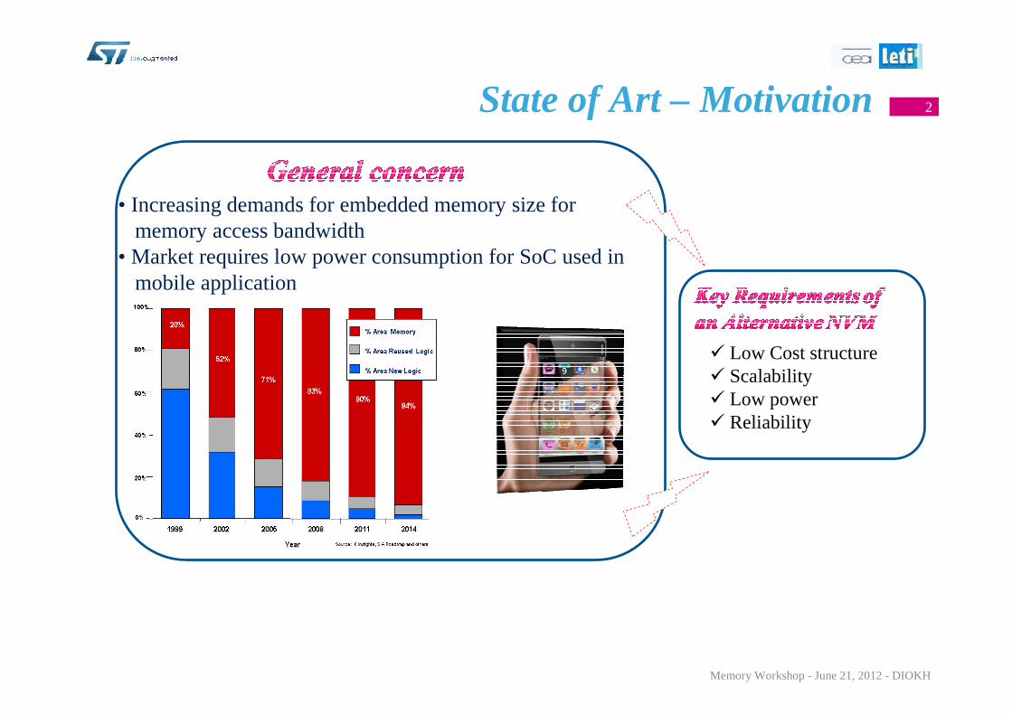
State of Art – Motivation
• Increasing demands for embedded memory size for memory access bandwidth
• Market requires low power consumption for SoC used in mobile application
2
� Low Cost structure� Scalability� Low power� Reliability
Memory Workshop - June 21, 2012 - DIOKH

State of Art – Motivation 3
Promising results showed on ReRAM in the literature
Panasonic: Bilayer-TaO based ReRAM using Platinum as electrodes
256Kbit CMOS 180nm, 10e9cycles,10year at 85°C
Samsung: Bilayer-TaO based ReRAM using Platinum as electrodes
Proposed physical model for TaO based on Schottky barrier modulation
Z. Wei et al, IEDM 2008
M-J. Lee et al., Nature Mat., 2011
Memory Workshop - June 21, 2012 - DIOKH

• Aim of the work: Demonstrate a TaO Based ReRAM which is :
• LOW COST NVM SOLUTION !
• All materials are cost effective and perfectly compatible with back-end process CMOS
• ReRAM structure based on mature process based on standard MIM• ReRAM integration just with two additional masks
• Extendable to very advanced CMOS technology (Sub 28nm)
• Endurant for application like MTP (multiple time programmable)
• Reliable
• Thermally stable
4State of Art – Motivation
Memory Workshop - June 21, 2012 - DIOKH

Outline
• State of the art and motivation
• Integration and functioning principle
• TaO properties impact on programming energies
• Mechanism of the switch / how to control the switch
• Switching speed, endurance and reliability
• Thermal behaviors
• Conclusion
5
Memory Workshop - June 21, 2012 - DIOKH

Integrated memory structures 6
ReRAM MIM, Fully CMOS 65nm compatible:
� Mature process integration�PEALD using TBTDET and Ar/O2 => TaO�PVD => TiN
� MIM area down to 1µm²
Ta2O5
TiN
TiN
Cross section TEM
TiNTaOx_5nm
TiN
V
TiNTaOx_10nm
TiN
V
TiNTa2O5_5nm
TiN
V
TiNTa2O5_10nm
TiN
V
Studied device splits
ReRAM device
Memory Workshop - June 21, 2012 - DIOKH

Switching characteristics 7
Critical parameters1.Forming (ON) operation :
• soft breakdown, creation of the critical conductive path• Should be compatible with of the select transistor characteristics
2.1st reset (OFF) current
I-V characteristics: Bipolar switching
Memory Workshop - June 21, 2012 - DIOKH

Study of forming voltage 8
Forming Voltage decreases with dielectric oxide thickness
� High forming voltage : device function on the weakness zone of MOS transistor
�TaOx leakage current higher than Ta2O5 on
� => Optimum Device : TiN/5nm-Ta2O5/TiNMemory Workshop - June 21, 2012 - DIOKH

TiN/5nm-Ta 2O5/TiN TiN/5nm-Ta 2O5/TiN
Conduction mechanism before Forming9
)*(lnln CVfE
JBE
TkA
E
J
B
PF →
=>+=
β
( ) ( ) )1
(ln1
lnT
fJBTk
EAJ
B
PF →=>+= β
(1)
(2)
Poole Frenkel modeling equations
(1) (2)
Straight lines behavior indicate Poole–Frenkel conduction mechanism
Memory Workshop - June 21, 2012 - DIOKH

Study of the Reset current 10
� Lowest 1st reset in thin dielectric
�TaOx shows a low reading window even if its reset current is lower than Ta205 reset current=> There after, studies will be focused only on results of TiN/5nm-Ta2O5/TiN device
Memory Workshop - June 21, 2012 - DIOKH

Outline
• State of the art and motivation
• Integration and functioning principle
• TaO properties impact on programming energies
• Mechanism of the switch / how to control the switch
• Switching speed, endurance and Reliability
• Thermal behaviors
• Conclusion
11
Memory Workshop - June 21, 2012 - DIOKH

Device area impact and possible mechanisms12
Ta205
TIN Top
V forming>0
VO 2+
gndTIN Bot
Or Vset>0
Ta205
TIN Top
Vreset< 0
VO 2+
gndTIN Bot
rupture
Local filament conduction path suggested � No issue for shrinkability
Memory Workshop - June 21, 2012 - DIOKH

Controlling the filament formation 13
Filament formation (ON state) could be controlled through current compliance in view of low power operation
� The resistance of the reset state can be controlled by the compliance current of the Set state
Memory Workshop - June 21, 2012 - DIOKH

Outline
• State of the art and motivation
• Integration and functioning principle
• TaO properties impact on programming energies
• Mechanism of the switch / how to control the switch
• Switching speed, endurance and Reliability
• Thermal behaviors
• Conclusion
14
Memory Workshop - June 21, 2012 - DIOKH
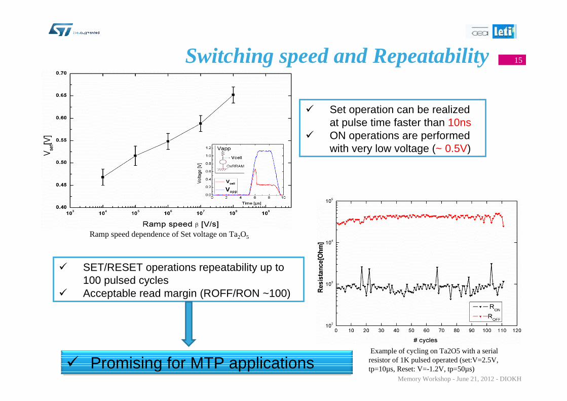
Switching speed and Repeatability15
Ramp speed dependence of Set voltage on Ta2O5
Example of cycling on Ta2O5 with a serial resistor of 1K pulsed operated (set:V=2.5V, tp=10µs, Reset: V=-1.2V, tp=50µs)
� SET/RESET operations repeatability up to 100 pulsed cycles
� Acceptable read margin (ROFF/RON ~100)
� Promising for MTP applications
� Set operation can be realized at pulse time faster than 10ns
� ON operations are performed with very low voltage (~ 0.5V)
Memory Workshop - June 21, 2012 - DIOKH

Retention at high temperature 16
� Cells store data after a bake of 250°C during 24ho urs� Cells are fully functional after the bake at 250°C during 24hours
Retention behavior of TiN/Ta2O5/TiN device under 250°C with constant read voltage of 0.1V
TiN/5nm-Ta 2O5/TiN
Memory Workshop - June 21, 2012 - DIOKH

Thermal stability: ON/OFF dependence with temperature
17
No significant impact of temperature on ON / OFF Resistance => Good thermal stability of 5nm - thickTa2O5 temperature up to 125°C
Temperature dependence of ON/OFF resistance of TiN/Ta2O5/TiN device (vread=0.1V) ON/OFF cycling dependence to temperature. Resistance values
(left coordinate axis) and Voltages values (right coordinate axis)
Memory Workshop - June 21, 2012 - DIOKH

Outline
• State of the art and motivation
• Integration and functioning principle
• TaO properties impact on programming energies
• Mechanism of the switch / how to control the switch
• Switching speed, endurance and Reliability
• Thermal behaviors
• Conclusion
18
Memory Workshop - June 21, 2012 - DIOKH

Conclusions• Forming and Reset operations have a close relationship with the TaO
properties and thicknesses
• Evidence of the filamentary conduction on TaO. Good shrinkability suggested
• ON/OFF operations demonstrated with very low voltage (0.5V) and high speed (10ns)
• Reliable devices ( ON/OFF retention during 24h at 250°C)
• Thermal stability (a key issue for SoC applications) is successfully demonstrated up to 125°C
19
TiN/Ta2-xO5-y/TiN structures are very promising for future MTP applications beyond 28 nm node technology
Memory Workshop - June 21, 2012 - DIOKH
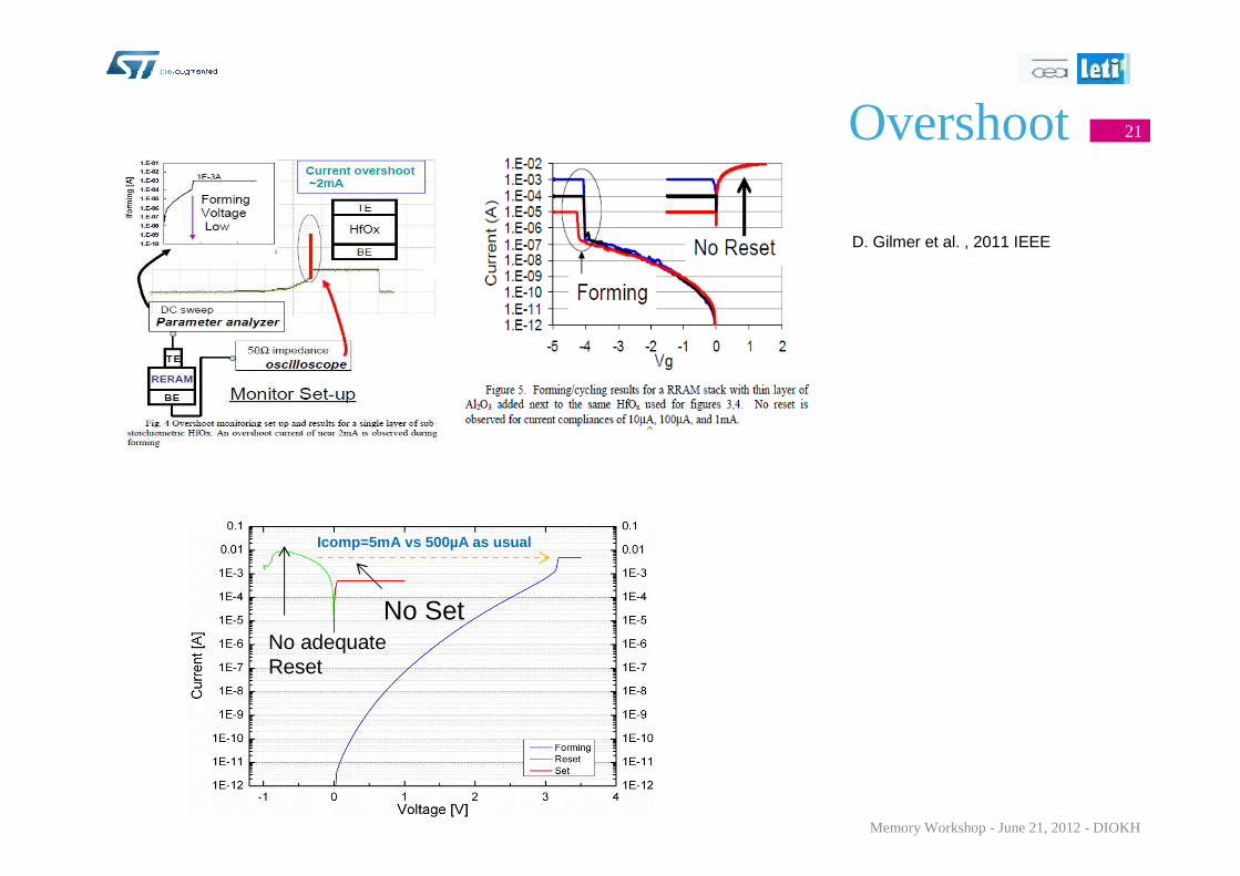
Overshoot
Icomp=5mA vs 500µA as usual
No SetNo adequate Reset
D. Gilmer et al. , 2011 IEEE
21
Memory Workshop - June 21, 2012 - DIOKH