Embed Size (px)
Citation preview
CHEMICAL ENGINEERING TRANSACTIONS
VOL. 43, 2015
A publication of
The Italian Association of Chemical Engineering Online at www.aidic.it/cet
Chief Editors: Sauro Pierucci, Jiří J. Klemeš Copyright © 2015, AIDIC Servizi S.r.l., ISBN 978-88-95608-34-1; ISSN 2283-9216
Electrodeposition and Characterization of Mo Oxide Nanostructures
Rosalinda Inguantaa, Tiziana Spanòa, Salvatore Piazzaa, Carmelo Sunseri*a, Francesco Barrecab, Enza Faziob, Fortunato Nerib, Letteria Silipignib aLaboratorio di Chimica Fisica Applicata, Dipartimento di Ingegneria Chimica Gestionale Informatica Meccanica, Università di Palermo, Viale delle Scienze - 90128 Palermo (Italy) b Laboratorio di Microanalisi, Dipartimento di Fisica e di Scienza della Terra, Università di Messina, Viale F. Stagno D'Alcontres, 98166 Messina (Italy) [email protected]
Template electrodeposition has been used to grow uniform arrays of molybdenum oxide nanostructures in polycarbonate membrane. Several parameters have been investigated, like electrodeposition, time and solution pH. These parameters do not influence the nature of the deposit that always consists of mixed valence molybdenum oxides, whereas the nanostructure morphology changes with pH. In particular, at low pH (2.7), nanotubes are formed, whilst arrays of nanowires are obtained above pH 5.5. This change of morphology is likely due to H2 bubbles evolution during the electrochemical deposition, particularly occurring at low pH. It was found that fast removal of H2 bubbles through vigorous stirring of the solution favors the growth of nanostructures with a uniform length. Molybdenum oxide nanostructures were characterized by XRD, EDS, Raman, XPS and photoelectrochemical measurements. Results indicate that nanostructures are amorphous and consist mainly of MoO2 underneath α-MoO3. The presence of these two oxides was confirmed by photoelectrochemical experiments. From photocurrent spectra, two linear regions appear in the (Iph·hν)0.5 vs. hν plot, whose extrapolation to Iph=0 gives optical gaps values of 2.5 and 3.2 eV, which are typical of MoO2 and α-MoO3, respectively. In addition, photoelectrochemical investigation revealed n-type conductivity of this mixed oxide deposit.
1. Introduction
Mo oxides are very interesting materials because they have widespread applications in several technological fields due their structural, electronic and optical properties (Saji and Lee, 2012). They are used in gas (NOx, CO, H2, and NH3) sensors (Ellefson et al., 2012), in sodium-ion batteries (Hariharan et al., 2013), in optoelectronic devices (Dukstiene and Sinkeviciute, 2013) and in electrochemical supercapacitors (Farsi et al., 2010). The specific properties of MoOx are enhanced at a nanosize scale as demonstrated in the case of nanostructured MoO2, showing excellent field-emission characteristics (Kumari et al., 2007), and in the case of MoO3 nanowires, that exhibited excellent catalytic properties (Dong et al., 2012). These exciting properties provide motivation for the development of a facile and simple method for preparing molybdenum oxide nanostructures. In the last years, we have shown that combination of electrodeposition process with template synthesis is a very good way to obtain nanostructures of very different materials (Inguanta et al., 2011). Here we extend this technique to the fabrication of Mo oxide nanostructures using polycarbonate membranes as template. At our best knowledge, our work is the first paper reporting fabrication of uniform MoOx nanowire arrays by template electrodeposition. Walter and co-workers (2003, 2005), using step decoration method, obtained MoOx (a mixture of MoO2 and MoO3 phases) nanofibers with diameters ranging from 20 nm to 1.3 μm on graphite surface. These oxide nanofibers were reduced to metallic Mo nanofibers in H2 atmosphere at 500°C or converted in MoS2 by exposure to H2S at 500-700°C. In those works nanofibers were obtained at the step edges of highly oriented pyrolitic graphite from which they were removed (about 80%) after embedding in
DOI: 10.3303/CET1543115
Please cite this article as: Inguanta R., Spano T., Piazza S., Sunseri C., Barreca F., Fazio E., Neri F., Silipigni L., 2015, Electrodeposition and characterization of mo oxide nanostructures, Chemical Engineering Transactions, 43, 685-690 DOI: 10.3303/CET1543115
685
polystyrene film. This process is possible only after reduction or conversion of MoOx nanofibers into metallic Mo or MoS2, whilst it was not possible to peel off directly MoOx nanofibers without destroy them, because they are brittle. In our method, nanowires of molybdenum oxide were obtained directly onto a Ni current collector and a well-defined and uniform array with very large surface area can be obtained simply after template dissolution. In particular, we fabricated molybdenum oxide nanowires from a molybdate aqueous solution; composition of the nanostructures was investigated by means of different characterization techniques (XRD, RAMAN, EDS, XPD and photoelectrochemistry). In fact, difficulty to establish the composition of electrodeposited product is well known owing to the formation of mixed valence molybdenum oxides, with the presence of nonstoichiometric oxides, (Saji and Lee, 2012). Also in (Walter et al., 2003) the as prepared nanowires were predominantly composed of MoO2 with the presence of MoO3, as revealed by XPS measurements. Even if deposition was carried out at a potential where Mo metal is thermodynamically stable, its presence in the deposit was excluded because Mo metal reacts promptly with water to produce MoO2 and H2 gas. These authors also showed that MoOx nanofibers have an amorphous nature. In a previous work (Silipigni et al., 2014) we reported the results of a systematic investigation carried out in order to check the influence of different deposition parameters (electrodeposition time, concentration of Mo precursor and solution pH). Here, the most important results will be discussed.
2. Experimental
Mo oxide nanostructures was obtained by electrodeposition in commercial track-etched polycarbonate membrane (Whatman, Cyclopore 47). These membranes have a nominal thickness of about 20 μm, a mean pore diameter of 200 nm. In order to fabricate the arrays of nanostructures a two-step procedure was employed. Initially, one side of the membrane was sputtered with gold and a Ni collector was deposited onto it by electrodeposition at -1.25 V(SCE), up to a thickness of about 35 μm. Then, the front surface of the membrane was immersed in a bath containing 50 g L-1 of (NH4)6Mo7O24·4H2O and electrodeposition was conducted at a cathodic current density of 2 mA/cm2 from 30 to 120 min. The electrochemical bath was prepared with ultrapure distilled water (18 MΩ cm) and the pH was adjusted at 2.7, 5.5 and 8.5. The crystallographic structure of Mo oxide NWs was investigated by X-ray analysis using an Ital-Structures diffractometer (mod. 1050). All diffractograms were obtained in the 2θ range from 10° to 100° with a step of 0.04° and a measuring time of 2 sec for step, using the copper Kα radiation (λ= 1.54 Å). Diffraction patterns were analyzed by comparison with ICDD database. Morphology was investigated using a scanning electron microscope (ESEM, FEI-QUANTA 200) equipped with an X-ray energy dispersive spectrometer (EDS). Length of the NWs after different electrodeposition times was estimated from the SEM cross-section pictures. SEM analysis was carried out after dissolution of the polycarbonate template in pure CHCl3 at room temperature. Before SEM observation, samples were sputter coated with a thin layer of gold in order to form a conducting film and to avoid electrostatic charging under the electron beam. Raman spectra were obtained at room temperature using a Renishaw (inVia Raman Microscope) spectrometer equipped with a microprobe (50x) and a CCD detector. The excitation was provided by the 633 nm line of a He:Ne laser and it was calibrated by means of polycrystalline Si. Power of the incident beam was 5 mW, and the width of the analysed spot for each sample was about 2 μm. Acquisition time was adjusted according to the intensity of the Raman scattering. The wave-number values reported in the spectra below have 1 cm-1 accuracy. For each experiment, Raman spectra were recorded at several points of the sample to ascertain its homogeneity. XPS was carried out in ultra high-vacuum condition (about 10-9 Torr) using a Thermo Scientific Instrument equipped with a monochromatic Al Kα source (hν=1486.6 eV) and a hemispherical analyser (spherical sector 180°). The constant-pass energy was set at 200 eV for survey scans and at 50 eV for the XPS core level spectra. Progressive removal of material layer was carried out using a scanning 3 KeV Ar+ ion gun, with a raster area of about 4 mm x 2 mm, until no substantial variations in the surface chemical composition were observed. Etching cycles of 10, 30, 90 and 270 s were performed to investigate changes in the nanostructure elemental composition from surface down to deeper layers. Photoelectrochemical behaviour of the films was investigated at room temperature in aerated 0.1 M Na2SO4 solution (pH=5.6), using the experimental set-up described elsewhere (Inguanta et al., 2010). Analysis was carried out using a cell having flat quartz windows for allowing sample illumination with a Pt wire counter electrode and a MSE reference electrode. Monochromatic irradiation was achieved using a UV-Vis Xenon lamp (Oriel). Photocurrent spectra reported below were corrected for the photon emission of the lamp/monochromator system at each wavelength; the latter was detected using a calibrated thermopile (Newport).
686
3. Results and Discussion
As reported in our previous work (Silipigni et al., 2014) stirring of the electrodeposition bath and its pH are the fundamental parameters that control the growth of nanostructures. In particular, stirring determines uniformity of nanostructures length, as can be seen in Table 1 showing nanostructures length vs. electrodeposition time in different electrodeposition conditions. For electrodepositions carried out in un-stirred solution, the lower uniformity of length may be attributed to the interference of hydrogen evolution, whose random bubble accumulation inside the polycarbonate pores causes the inhibition of deposition. It is well-known that the occurrence of this reaction leads to an increase of the interfacial pH up to very basic value. To overcome this limitation, electrodeposition was performed in a stirred bath that favours the removal of H2 bubbles from nano-channels. As is evident from Table 1, this arrangement allows obtaining nanostructures with uniform length along the entire deposition area. Table 1 also shows that NWs mean length increases with the electrodeposition time, whilst the average growth rate decreases. This behaviour may be attributed to the low electrical conductivity of the deposit determining a progressive increase of the ohmic drop, which in turn modifies current distribution favouring the secondary reaction of H2 evolution.
Table 1: Nanostructures length (μm) vs. electrodeposition time (min) obtained in different electrodeposition conditions. In parentheses, the mean growth rate of nanostructures (nm min-1) is also reported.
Time Un-stirred solution Stirred solution pH =2.7 pH= 5.5 pH=8.5 30 1.05±0.14
(0.035) 2.14±0.11 (0.071)
8.02±0.13 (0.267)
2.14±0.11 (0.071)
1.34±0.24 (0.045)
60 1.56±0.64 (0.026)
2.45±0.16 (0.041)
120 2.78±1.22 (0.023)
3.63±0.21 (0.03)
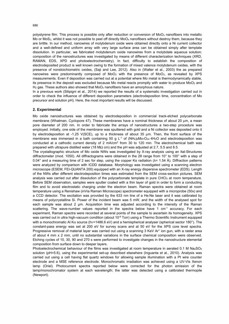
Figure 1: SEM images of Mo oxide nanostructures obtained at different solution pH: (a) pH 2.7; (b) pH 5.5; (c) pH 8.5; (d) tilted-view of nanostructures obtained at pH 5.5.
687
As for the influence of bath pH, we have found that this parameter controls both length of the nanostructures (Table 1) and their morphology (Figure 1). Longer nanostructures were obtained at lower pH, but they consisted only of nanotubes with a smooth surface and a wall thickness of about 37±11 nm (Figure 1a). Likely, their collapse was due to a poor mechanical stability because of the thin wall. The formation of nanotubes at low pH was likely due to the vigorous H2 evolution, occurring inside the pores, which confined deposition only in the gap between pore wall and gas bubbles. At pH 5.5, NWs were formed as shown in Figure 2b: this image evidences a cylindrical shape fairly regular and slightly wrinkled. Besides, wires of different diameters are clearly visible, from this image we calculated a mean diameter of 220±20 nm. Interconnection between different wires, due to the typical morphology of the polycarbonate template channels, is also visible. The tilted image reported in Figure 2d details better morphology of nanowires firmly connected to Ni substrate. Also at pH 8.5 nanowires were obtained (Figure 2c), but we found non-uniform length of nanowires, probably due to slow deposition kinetics, as reported by McEvoy and Stevenson (2004). XRD characterization reveals that in all deposition conditions nanostructures consist of an amorphous phase; thus Raman and XPS analysis were also performed for identifying composition of deposit. In Table 2 the different phases identified by Raman spectra are listed. In all deposition conditions, the Raman modes characteristic of MoO2 and MoO3 were revealed. Moreover, changing solution, pH oxides with different hydration degree were formed. A less hydrated oxide was likely obtained at pH 5.5 as revealed by the presence of the Raman mode of MoO3·(1/3)H2O and MoO3·H2O. On the other hand, deposit formed at pH 2.7 and 8.5 show modes of MoO3·H2O and MoO3·(1/2)H2O. From these results, it can be concluded that in all conditions, nanostructures consist of mixed amorphous MoO3 and MoO2 with the presence also of differently hydrated oxide.
Table 2: Different phases revealed by Raman spectroscopy.
Time pH =2.7 pH= 5.5 pH=8.5 MoO2 x X x α-MoO3 x X x MoO3-x x x MoO31/3H20 X MoO31/2H20 x x MoO3H20 x X x
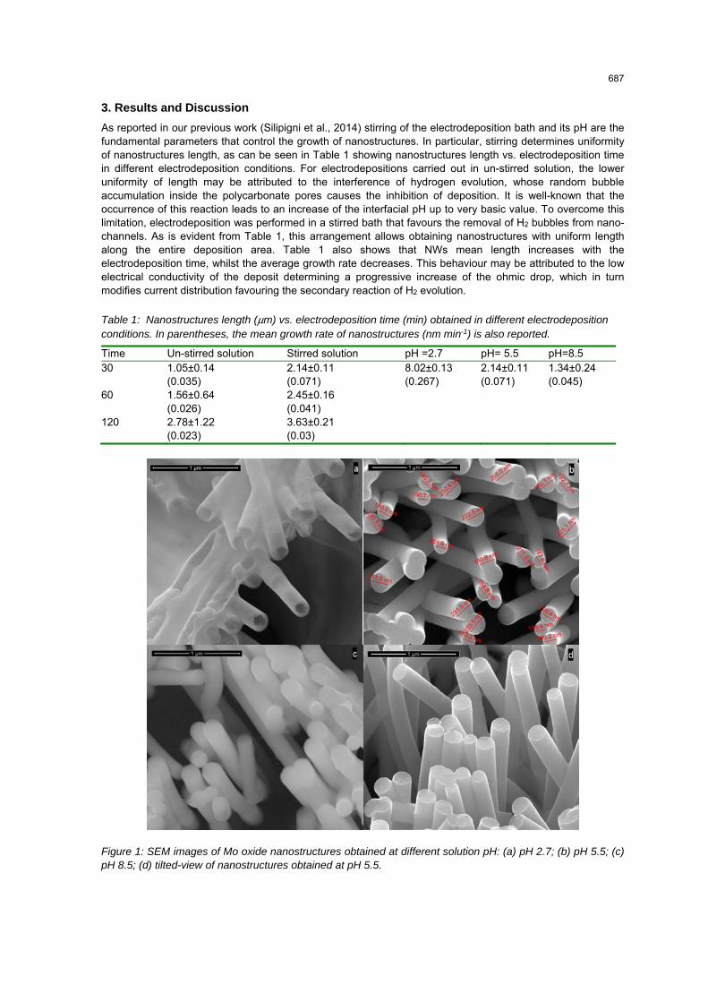
In order to confirm these results, we have also carried out XPS measurements. Figure 2a shows the XPS atomic percent-etching time profile for the Mo oxide nanostructures obtained at pH 5.5. A carbon contamination, due to residual polycarbonate, was observed and it decreases with etching time. Nickel, from the electrodeposited film on the gold layer, and gold, from the layer sputtered onto the membrane surface, were also found on nanostructures surface, with concentrations increasing with the etching time. Initially, molybdenum and oxygen concentrations increase with the etching time, but then they reach stabilized values. In order to distinguish the chemical state of molybdenum ions at the different etching times, the evolution of the Mo 3d core level was examined as a function of etching time, as illustrated in Figure 2b.
Figure 2: (a) XPS atomic percent-etching time profile for the Mo oxide nanostructures obtained at pH 5.5; (b) Evolution of Mo 3d core level XPS spectra as a function of etching time.
688
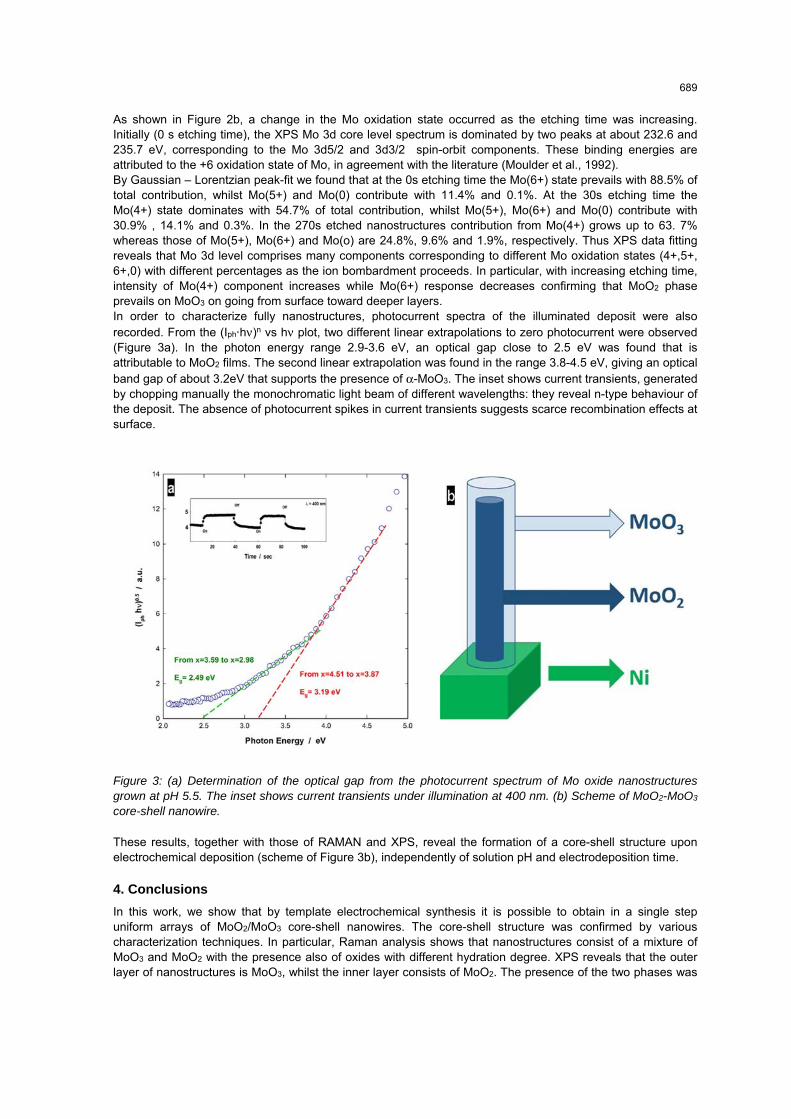
As shown in Figure 2b, a change in the Mo oxidation state occurred as the etching time was increasing. Initially (0 s etching time), the XPS Mo 3d core level spectrum is dominated by two peaks at about 232.6 and 235.7 eV, corresponding to the Mo 3d5/2 and 3d3/2 spin-orbit components. These binding energies are attributed to the +6 oxidation state of Mo, in agreement with the literature (Moulder et al., 1992). By Gaussian – Lorentzian peak-fit we found that at the 0s etching time the Mo(6+) state prevails with 88.5% of total contribution, whilst Mo(5+) and Mo(0) contribute with 11.4% and 0.1%. At the 30s etching time the Mo(4+) state dominates with 54.7% of total contribution, whilst Mo(5+), Mo(6+) and Mo(0) contribute with 30.9% , 14.1% and 0.3%. In the 270s etched nanostructures contribution from Mo(4+) grows up to 63. 7% whereas those of Mo(5+), Mo(6+) and Mo(o) are 24.8%, 9.6% and 1.9%, respectively. Thus XPS data fitting reveals that Mo 3d level comprises many components corresponding to different Mo oxidation states (4+,5+, 6+,0) with different percentages as the ion bombardment proceeds. In particular, with increasing etching time, intensity of Mo(4+) component increases while Mo(6+) response decreases confirming that MoO2 phase prevails on MoO3 on going from surface toward deeper layers. In order to characterize fully nanostructures, photocurrent spectra of the illuminated deposit were also recorded. From the (Iph·hν)n vs hν plot, two different linear extrapolations to zero photocurrent were observed (Figure 3a). In the photon energy range 2.9-3.6 eV, an optical gap close to 2.5 eV was found that is attributable to MoO2 films. The second linear extrapolation was found in the range 3.8-4.5 eV, giving an optical band gap of about 3.2eV that supports the presence of α-MoO3. The inset shows current transients, generated by chopping manually the monochromatic light beam of different wavelengths: they reveal n-type behaviour of the deposit. The absence of photocurrent spikes in current transients suggests scarce recombination effects at surface.
Figure 3: (a) Determination of the optical gap from the photocurrent spectrum of Mo oxide nanostructures grown at pH 5.5. The inset shows current transients under illumination at 400 nm. (b) Scheme of MoO2-MoO3 core-shell nanowire.
These results, together with those of RAMAN and XPS, reveal the formation of a core-shell structure upon electrochemical deposition (scheme of Figure 3b), independently of solution pH and electrodeposition time.
4. Conclusions
In this work, we show that by template electrochemical synthesis it is possible to obtain in a single step uniform arrays of MoO2/MoO3 core-shell nanowires. The core-shell structure was confirmed by various characterization techniques. In particular, Raman analysis shows that nanostructures consist of a mixture of MoO3 and MoO2 with the presence also of oxides with different hydration degree. XPS reveals that the outer layer of nanostructures is MoO3, whilst the inner layer consists of MoO2. The presence of the two phases was
689
confirmed by photoelectrochemical measurements, showing anodic photocurrent and two thresholds at 2.5 and 3.2 eV, corresponding to the optical gap of MoO2 and MoO3, respectively. Morphology of the nanostructures was influenced by stirring of the solution and by its pH. In particular, we showed that it is possible to obtain both nanotubes (at low pH) and nanowires (at pH greater than 5.5). Stirred solution at pH 5.5 is the better condition for deposition, because it results in the formation of core-shell nanostructures uniformly distributed over the entire area.
Acknowledgements
The European Community partially funded this work through Programma Operativo Nazionale Ricerca e Competitività 2007-2013 (PON02_00355_3391233 Project).
References
Dong, W., Huang, H.; Zhu, Y.; Li, X.; Wang, X.; Li, C.; Chen, B.; Wang, G.; Shi, Z. Room-Temperature Solution Synthesis of Ag Nanoparticle Functionalized Molybdenum Oxide Nanowires and their Catalytic Applications. Nanotechnology. 2012, 23, 425602.
Dukstiene, N.; Sinkeviciute, D. Photoelectrochemical Properties of MoO2 Thin Films. J. Solid State Electrochem. 2013, 17, 1175-1184.
Ellefson, C. A.; Marin-Flores, O.; Ha, S.; Norton, M. G. Synthesis and Applications of Molybdenum (IV) Oxide. J. Mater. Sci. 2012, 47, 2057-2071.
Farsi, H.; Gobal, F.; Raissi, H.; Moghiminia, S. On the Pseudocapacitive Behavior of Nanostructured Molybdenum Oxide. J. Solid State Electrochem. 2010, 14, 643-650.
Hariharan, S.; Saravanan, K.; Balaya, P. -MoO3: A High Performance Anode Material for Sodium-Ion Batteries. Electrochem. Commun. 2013, 31, 5-9.
Inguanta, R., Ferrara, G., Piazza, S., Sunseri, C., Fabrication and characterization of metal and metal oxide nanostructures grown by metal displacement deposition into anodic alumina membranes, Chemical Engineering Transactions, 2011, 24, 199-204.
Kumari, L.; Ma, Y-R.; Tsai, C-C.; Lin, Y-W.; Wu, S. Y.; Cheng, K-W.; Liou, Y. X-ray Diffraction and Raman Scattering Studies on Lange-area Array and Nanobranched Structure of 1D MoO2 Nanorods. Nanotechnology. 2007, 18, 115717.
Li, Q.; Walter, EC.; van der Veer, WE.; Murray, BJ.; Newberg, JT.; Bohannan, EW.; Switzer, JA.; Hemminger, JC.; Penner, RM. 2005, Molybdenum disulfide nanowires and nanoribbons by electrochemical/chemical synthesis, J Phys Chem B., 109, 3169-82.
McEvoy T.M. and Stevenson, K. J. Elucidation of the electrodeposition mechanism of molybdenum oxide from iso- and peroxo-polymolybdate solutions, J Mater. Res. 19 (2004) 429-438
Moulder J.F.; Stikle, W.F.; Sobol P.E.; Bomben, K.D. in Handbook of X-ray Photoelectron Spectroscopy, edited by J. Chastain, Perkin-Elmer Corporation, Minesota, 1992
Saji, V. S.; Lee, C-W. Molybdenum, Molybdenum Oxides, and their Electrochemistry, ChemSusChem. 2012, 5, 1146-1161.
Silipigni L., Barreca F., Fazio E., Neri F., Spanò T., Piazza S:, Sunseri C., Inguanta R., 2014, Template electrochemical growth and properties of Mo oxide nanostructures, J. Phyc. Chem. C, 118, 22299-22308.
Walter E.C.; Zach M.P., Favier F., Murray B.J.; Inazu, K.; Hemminger, J.C., Penner, R.M., 2003, Metal nanowire arrays by electrodeposition, ChemPhysChem 4, 131-138.
690


![Electrodeposition of Zn-Mn alloys from recycling battery leach … · 2014. 5. 20. · recovery by electrodeposition [1–4] is currently being studied in our laboratory [5]. Electrodeposition](https://img.pdfslide.us/doc/110x75/6112e3e4b1654c15ca54266d/electrodeposition-of-zn-mn-alloys-from-recycling-battery-leach-2014-5-20-recovery.jpg)