Embed Size (px)
Citation preview
Electrodeposition
Andre Avelino PasaThin Films and Surfaces Group, Departamento de Fısica, Universidade Federal de SantaCatarina, Florianopolis, Santa Catarina, Brazil
Maximiliano Luis MunfordGroup of Organic Optoelectronic Devices, Departamento de Fısica, Universidade Federal doParana, Curitiba, Parana, Brazil
INTRODUCTION
Most important concepts and techniques of an electro-deposition are introduced and described here in aneasy-to-understand way. Examples of technologicalapplications are given, with emphasis on the fabri-cation of nanostructures.
DEFINITIONS AND HISTORY
Electrodeposition is an electrochemical process thatallows the preparation of solid deposits on the surfaceof conductive materials. It is a commercially highlyrelevant process, providing the basis for many indus-trial applications, such as electro-winning, refining,and metal plating. Metal plating is the process thathas perhaps the closest contact with most people’severyday life, because we are surrounded by things thathave a protective or decorative coating, such aswatches, buttons, belt buckles, doorknobs, handlebars,etc. Additionally and more recently, as will be seenbelow, not only do the circuit boards and the packagingmodules of computers, but also the recording andreading heads of their hard disk drives and the micro-processor chip itself may have plated material on them.
Electrodeposits are formed by the action of an elec-tric current passing in an electrochemical cell, a devicethat consists of two conductive or semi-conductingelectrodes immersed in an electrolyte. The electrodesare called the working electrode (cathode), consistingof the object where electrodeposition is planned, andthe counter-electrode (anode), necessary to completethe electrical circuit. Electrolytes for electrodepositionare usually aqueous solutions containing positive andnegative ions, prepared by dissolving metal salts. Theelectric current that flows between the two conductiveelectrodes in the presence of an external voltage isbecause of the motion of charged species, via migrationand diffusion, towards the surfaces of the polarized elec-trodes. At the surface of the electrodes, the conductionmechanism must change from ionic to electronic, an
interface process mediated by the occurrence of elec-trochemical reactions that promote the reduction orthe oxidation (redox reactions) of the ionic species.
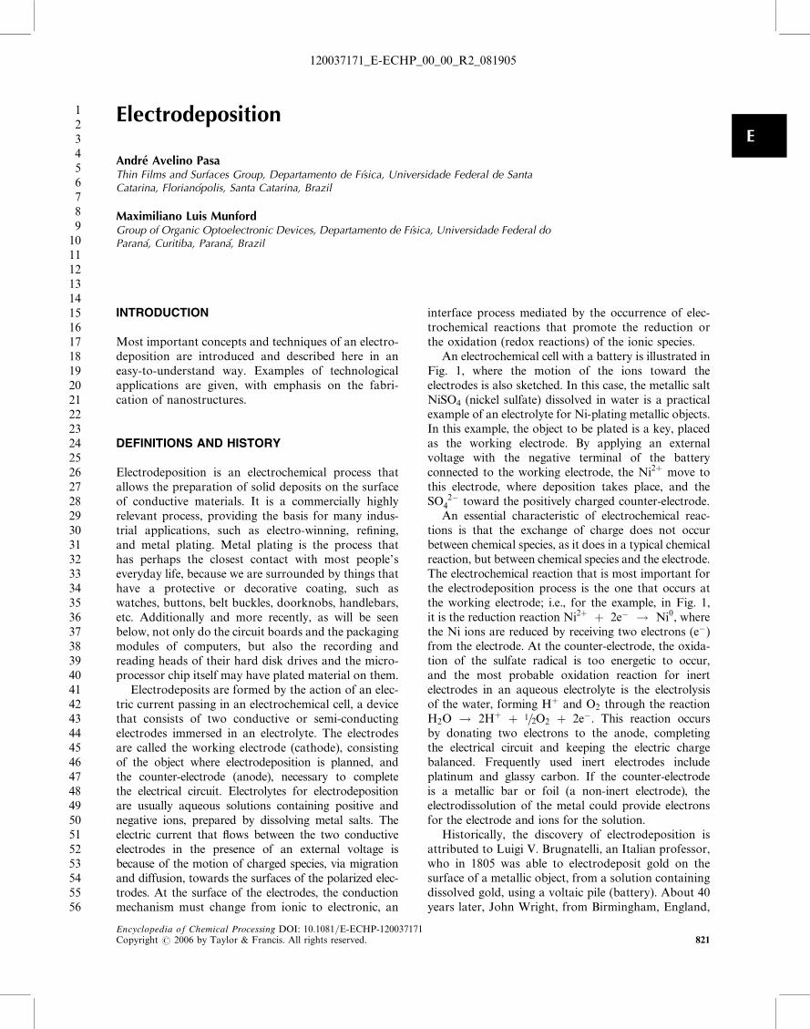
An electrochemical cell with a battery is illustrated inFig. 1, where the motion of the ions toward theelectrodes is also sketched. In this case, the metallic saltNiSO4 (nickel sulfate) dissolved in water is a practicalexample of an electrolyte for Ni-plating metallic objects.In this example, the object to be plated is a key, placedas the working electrode. By applying an externalvoltage with the negative terminal of the batteryconnected to the working electrode, the Ni2þ move tothis electrode, where deposition takes place, and theSO 2�
4 toward the positively charged counter-electrode.An essential characteristic of electrochemical reac-
tions is that the exchange of charge does not occurbetween chemical species, as it does in a typical chemicalreaction, but between chemical species and the electrode.The electrochemical reaction that is most important forthe electrodeposition process is the one that occurs atthe working electrode; i.e., for the example, in Fig. 1,it is the reduction reaction Ni2þ þ 2e� ! Ni0, wherethe Ni ions are reduced by receiving two electrons (e�)from the electrode. At the counter-electrode, the oxida-tion of the sulfate radical is too energetic to occur,and the most probable oxidation reaction for inertelectrodes in an aqueous electrolyte is the electrolysisof the water, forming Hþ and O2 through the reactionH2O ! 2Hþ þ 1=2O2 þ 2e�. This reaction occursby donating two electrons to the anode, completingthe electrical circuit and keeping the electric chargebalanced. Frequently used inert electrodes includeplatinum and glassy carbon. If the counter-electrodeis a metallic bar or foil (a non-inert electrode), theelectrodissolution of the metal could provide electronsfor the electrode and ions for the solution.
Historically, the discovery of electrodeposition isattributed to Luigi V. Brugnatelli, an Italian professor,who in 1805 was able to electrodeposit gold on thesurface of a metallic object, from a solution containingdissolved gold, using a voltaic pile (battery). About 40years later, John Wright, from Birmingham, England,
Encyclopedia of Chemical Processing DOI: 10.1081/E-ECHP-120037171Copyright # 2006 by Taylor & Francis. All rights reserved. 821
E
123456789
1011121314151617181920212223242526272829303132333435363738394041424344454647484950515253545556
120037171_E-ECHP_00_00_R2_081905
discovered that potassium cyanide was a suitableelectrolyte for gold and silver electroplating. Thisdiscovery made electrodeposition an important com-mercial process for covering the surface of variouskinds of metallic object with thin coatings of metalsfor corrosion protection and decorative purposes. Sub-sequently, baths for the deposition of other metals andalloys such as nickel, zinc, tin, and brass (an alloyconsisting essentially of copper and zinc in variableproportions) were developed. For the next 100 years,the main idea was to use electrodeposition for coveringthe surface of inexpensive materials with a thin layer ofa noble metal. By the 1940s, however, electrodeposi-tion was rediscovered by the electronics industry. Theelectrodeposition of gold for electronic componentswas a totally different kind of application of electrode-position techniques.
Over the years, electrodeposition became a highlydeveloped process. Direct current (DC) power supplieswere developed; anodic and cathodic reactions weredescribed; new safer baths based on acid electrolytes,avoiding the earlier poisonous cyanide-based ones werediscovered; models for the deposition process incorpor-ating mass transport to the electrodes, charge transferkinetics, and nucleation and growth at the working elec-trode were developed; and regulatory rules for wastewater emission and waste disposal were created. Simul-taneously, a gradual improvement in electrodepositionfor large scale manufacturing processes took place.
ELECTRODEPOSITION APPARATUSAND CONCEPTS
Electrodeposition on the industrial scale requires anelectrochemical cell and a DC current power supply.
This approach is relatively simple and inexpensive,and is known as galvanostatic plating system, becausethe current between the electrodes is controlled (main-tained constant). Another important deposition modeis the pontentiostatic one. This mode is a consequenceof the development of electrochemical science, whereelectrochemical reactions at the surfaces of electrodesare carefully investigated. The electrochemist devel-oped reference electrodes, in order to measure thepotential drop near the surface of electrodes. Assumingthat the electrolyte contains sufficient ions (has suffi-ciently high conductivity) to avoid any ohmic voltagedrop, because of the resistance of the electrolytebetween the electrodes, all the voltage applied by thebattery (in Fig. 1) will appear near the surface of theelectrodes, where a charged region is formed (usuallynamed the double layer). It is very important to mea-sure the voltage drop across these charged regions,because it controls the driving force for phase transfor-mation from ion to reduced state. A simple metal foilcould be used as a reference electrode; however,because of the need to have a standard electrode tomeasure potential drops at the surface of differenttypes of working electrode in contact with differentelectrolytes, a hydrogen electrode was elected, andnow all electrode potentials are quoted relative to thisarbitrarily chosen reference electrode. What is alwaysmeasured is the potential difference between twoelectrodes. By defining the potential of the hydrogenelectrode as zero, it is possible to generate a table ofall the possible redox reaction potentials relative to thiselectrode, and these potentials are called standardpotentials. The standard hydrogen electrode (SHE),which is usually constructed by bubbling hydrogengas over an immersed platinum foil, has its operationbased on the redox reaction H2 $ 2Hþ þ 2e�.Other reference electrodes that are robust, stable, andeasily constructed than the SHE are frequently usedin the laboratory, give potential measurements thatcan be converted to standard potentials by adding orsubtracting a constant value. The most common arethe calomel electrode (Hg=Hg2Cl2) and silver=silverchloride electrode (Ag=AgCl).
The potential of an electrochemical cell, also knownas the cell potential or electromotive force (emf) is thesum of the potential drops at the cathode and anode,where the reduction and oxidation reactions occur.With the introduction of a reference electrode thepotentials of these two electrodes can be measuredindependently, allowing the independent investigationof the reactions that are taking place at each electrode(working or counter). These redox reactions are calledhalf-cell reactions or simply half-reactions. The half-reaction potential E 0 can be measured with a SHEelectrode at standard conditions, i.e., at electrolyteconcentrations of 1M, gas pressures of 1 atm., and
Ni++ SO4–
ELECTROCHEMICAL CELL
Electrolyte
BATTERY
electrons electrons
WorkingElectrode
CounterElectrode
– +
Fig. 1 Positively charged nickel ions in the electrolyte areattracted by the negatively charged key (working electrode).At the surface of the key they are reduced by gaining two
electrons, and metal is deposited.
AQ1/
PR
822 Electrodeposition
123456789
1011121314151617181920212223242526272829303132333435363738394041424344454647484950515253545556
120037171_E-ECHP_00_00_R2_081905
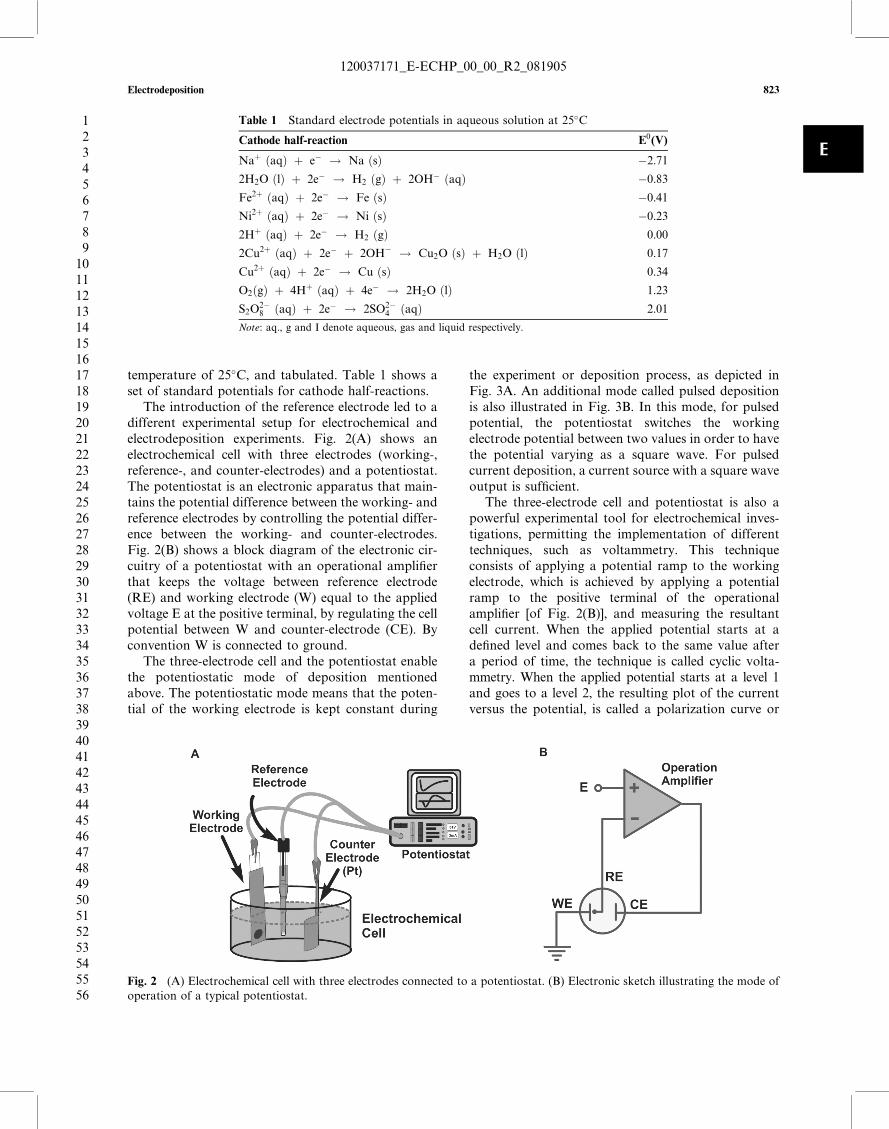
temperature of 25�C, and tabulated. Table 1 shows aset of standard potentials for cathode half-reactions.
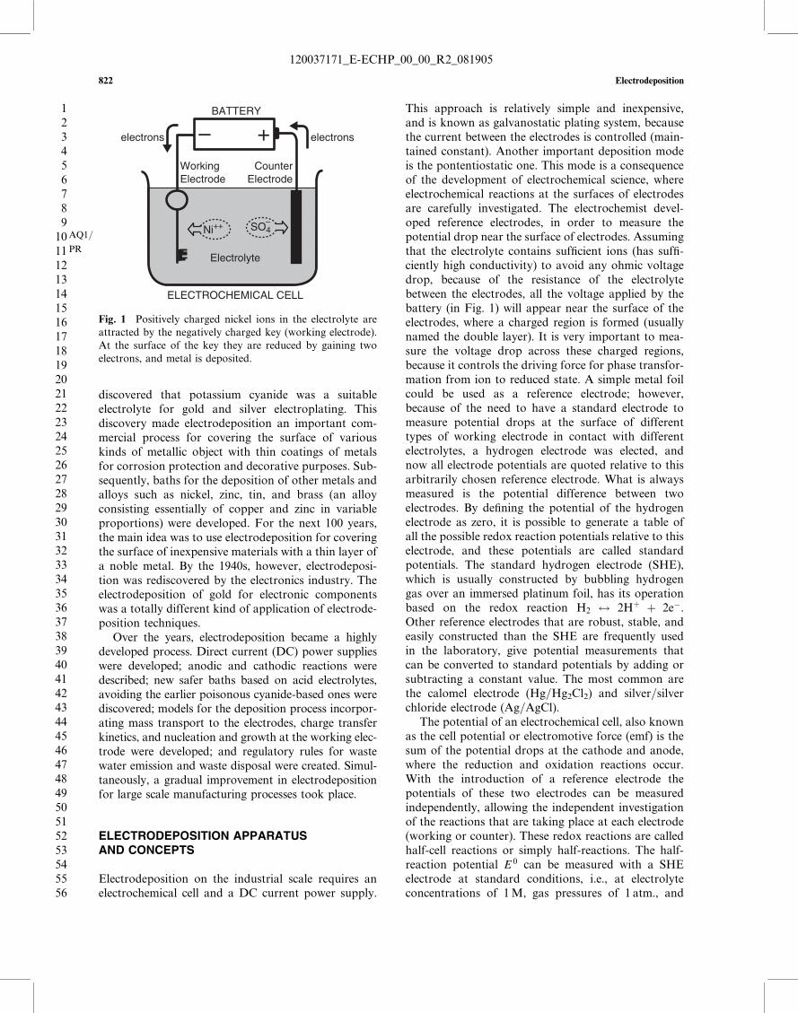
The introduction of the reference electrode led to adifferent experimental setup for electrochemical andelectrodeposition experiments. Fig. 2(A) shows anelectrochemical cell with three electrodes (working-,reference-, and counter-electrodes) and a potentiostat.The potentiostat is an electronic apparatus that main-tains the potential difference between the working- andreference electrodes by controlling the potential differ-ence between the working- and counter-electrodes.Fig. 2(B) shows a block diagram of the electronic cir-cuitry of a potentiostat with an operational amplifierthat keeps the voltage between reference electrode(RE) and working electrode (W) equal to the appliedvoltage E at the positive terminal, by regulating the cellpotential between W and counter-electrode (CE). Byconvention W is connected to ground.
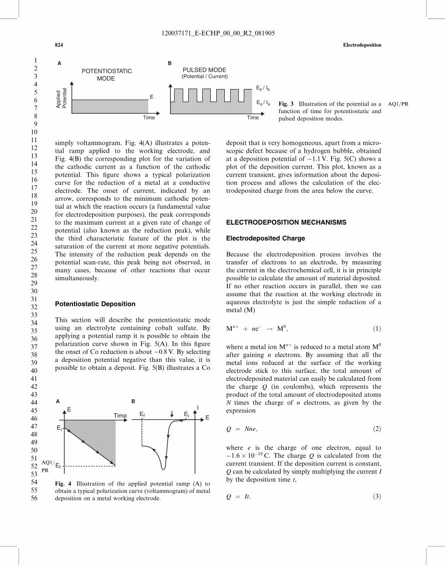
The three-electrode cell and the potentiostat enablethe potentiostatic mode of deposition mentionedabove. The potentiostatic mode means that the poten-tial of the working electrode is kept constant during
the experiment or deposition process, as depicted inFig. 3A. An additional mode called pulsed depositionis also illustrated in Fig. 3B. In this mode, for pulsedpotential, the potentiostat switches the workingelectrode potential between two values in order to havethe potential varying as a square wave. For pulsedcurrent deposition, a current source with a square waveoutput is sufficient.
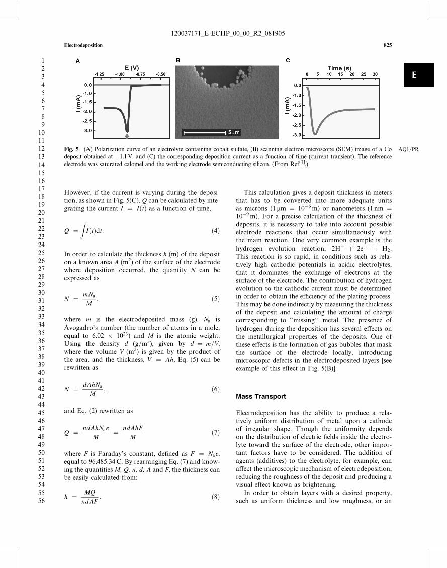
The three-electrode cell and potentiostat is also apowerful experimental tool for electrochemical inves-tigations, permitting the implementation of differenttechniques, such as voltammetry. This techniqueconsists of applying a potential ramp to the workingelectrode, which is achieved by applying a potentialramp to the positive terminal of the operationalamplifier [of Fig. 2(B)], and measuring the resultantcell current. When the applied potential starts at adefined level and comes back to the same value aftera period of time, the technique is called cyclic volta-mmetry. When the applied potential starts at a level 1and goes to a level 2, the resulting plot of the currentversus the potential, is called a polarization curve or
Table 1 Standard electrode potentials in aqueous solution at 25�C
Cathode half-reaction E0(V)
Naþ ðaqÞ þ e� ! Na ðsÞ �2.71
2H2O ðlÞ þ 2e� ! H2 ðgÞ þ 2OH� ðaqÞ �0.83
Fe2þ ðaqÞ þ 2e� ! Fe ðsÞ �0.41
Ni2þ ðaqÞ þ 2e� ! Ni ðsÞ �0.23
2Hþ ðaqÞ þ 2e� ! H2 ðgÞ 0.00
2Cu2þ ðaqÞ þ 2e� þ 2OH� ! Cu2O ðsÞ þ H2O ðlÞ 0.17
Cu2þ ðaqÞ þ 2e� ! Cu ðsÞ 0.34
O2ðgÞ þ 4Hþ ðaqÞ þ 4e� ! 2H2O ðlÞ 1.23
S2O2�8 ðaqÞ þ 2e� ! 2SO2�
4 ðaqÞ 2.01
Note: aq., g and I denote aqueous, gas and liquid respectively.
Fig. 2 (A) Electrochemical cell with three electrodes connected to a potentiostat. (B) Electronic sketch illustrating the mode ofoperation of a typical potentiostat.
Electrodeposition 823
E
123456789
1011121314151617181920212223242526272829303132333435363738394041424344454647484950515253545556
120037171_E-ECHP_00_00_R2_081905
simply voltammogram. Fig. 4(A) illustrates a poten-tial ramp applied to the working electrode, andFig. 4(B) the corresponding plot for the variation ofthe cathodic current as a function of the cathodicpotential. This figure shows a typical polarizationcurve for the reduction of a metal at a conductiveelectrode. The onset of current, indicated by anarrow, corresponds to the minimum cathodic poten-tial at which the reaction occurs (a fundamental valuefor electrodeposition purposes), the peak correspondsto the maximum current at a given rate of change ofpotential (also known as the reduction peak), whilethe third characteristic feature of the plot is thesaturation of the current at more negative potentials.The intensity of the reduction peak depends on thepotential scan-rate, this peak being not observed, inmany cases, because of other reactions that occursimultaneously.
Potentiostatic Deposition
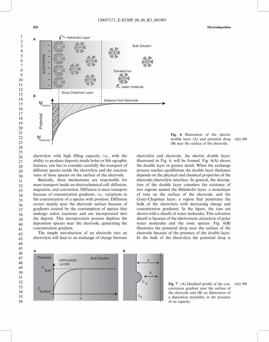
This section will describe the pontentiostatic modeusing an electrolyte containing cobalt sulfate. Byapplying a potential ramp it is possible to obtain thepolarization curve shown in Fig. 5(A). In this figurethe onset of Co reduction is about �0.8V. By selectinga deposition potential negative than this value, it ispossible to obtain a deposit. Fig. 5(B) illustrates a Co
deposit that is very homogeneous, apart from a micro-scopic defect because of a hydrogen bubble, obtainedat a deposition potential of �1.1V. Fig. 5(C) shows aplot of the deposition current. This plot, known as acurrent transient, gives information about the deposi-tion process and allows the calculation of the elec-trodeposited charge from the area below the curve.
ELECTRODEPOSITION MECHANISMS
Electrodeposited Charge
Because the electrodeposition process involves thetransfer of electrons to an electrode, by measuringthe current in the electrochemical cell, it is in principlepossible to calculate the amount of material deposited.If no other reaction occurs in parallel, then we canassume that the reaction at the working electrode inaqueous electrolyte is just the simple reduction of ametal (M)
Mnþ þ ne� ! M0; ð1Þ
where a metal ion Mnþ is reduced to a metal atom M0
after gaining n electrons. By assuming that all themetal ions reduced at the surface of the workingelectrode stick to this surface, the total amount ofelectrodeposited material can easily be calculated fromthe charge Q (in coulombs), which represents theproduct of the total amount of electrodeposited atomsN times the charge of n electrons, as given by theexpression
Q ¼ Nne; ð2Þ
where e is the charge of one electron, equal to�1:6� 10�19 C. The charge Q is calculated from thecurrent transient. If the deposition current is constant,Q can be calculated by simply multiplying the current Iby the deposition time t,
Q ¼ It: ð3Þ
PULSED MODE(Potential / Current)
TimeTime
App
lied
Pot
entia
l POTENTIOSTATIC
MODE
E
A B
Eb / Ib
Ea / Ia Fig. 3 Illustration AQ1=PRof the potential as afunction of time for potentiostatic and
pulsed deposition modes.
E
IEi
Ei
Ef
Ef
TimeE
A B
Fig. 4 Illustration of the applied potential ramp (A) toobtain a typical polarization curve (voltammogram) of metaldeposition on a metal working electrode.
AQ1/
PR
824 Electrodeposition
123456789
1011121314151617181920212223242526272829303132333435363738394041424344454647484950515253545556
120037171_E-ECHP_00_00_R2_081905
However, if the current is varying during the deposi-tion, as shown in Fig. 5(C), Q can be calculated by inte-grating the current I ¼ IðtÞ as a function of time,
Q ¼ZIðtÞdt: ð4Þ
In order to calculate the thickness h (m) of the depositon a known area A (m2) of the surface of the electrodewhere deposition occurred, the quantity N can beexpressed as
N ¼ mNa
M; ð5Þ
where m is the electrodeposited mass (g), Na isAvogadro’s number (the number of atoms in a mole,equal to 6:02 � 1023) and M is the atomic weight.Using the density d (g=m3), given by d ¼ m=V,where the volume V (m3) is given by the product ofthe area, and the thickness, V ¼ Ah, Eq. (5) can berewritten as
N ¼ dAhNa
M; ð6Þ
and Eq. (2) rewritten as
Q ¼ ndAhNae
M¼ ndAhF
Mð7Þ
where F is Faraday’s constant, defined as F ¼ Nae,equal to 96,485.34C. By rearranging Eq. (7) and know-ing the quantitiesM, Q, n, d, A and F, the thickness canbe easily calculated from:
h ¼ MQ
ndAF: ð8Þ
This calculation gives a deposit thickness in metersthat has to be converted into more adequate unitsas microns (1 mm ¼ 10�6m) or nanometers (1 nm ¼10�9m). For a precise calculation of the thickness ofdeposits, it is necessary to take into account possibleelectrode reactions that occur simultaneously withthe main reaction. One very common example is thehydrogen evolution reaction, 2Hþ þ 2e� ! H2.This reaction is so rapid, in conditions such as rela-tively high cathodic potentials in acidic electrolytes,that it dominates the exchange of electrons at thesurface of the electrode. The contribution of hydrogenevolution to the cathodic current must be determinedin order to obtain the efficiency of the plating process.This may be done indirectly by measuring the thicknessof the deposit and calculating the amount of chargecorresponding to ‘‘missing’’ metal. The presence ofhydrogen during the deposition has several effects onthe metallurgical properties of the deposits. One ofthese effects is the formation of gas bubbles that maskthe surface of the electrode locally, introducingmicroscopic defects in the electrodeposited layers [seeexample of this effect in Fig. 5(B)].
Mass Transport
Electrodeposition has the ability to produce a rela-tively uniform distribution of metal upon a cathodeof irregular shape. Though the uniformity dependson the distribution of electric fields inside the electro-lyte toward the surface of the electrode, other impor-tant factors have to be considered. The addition ofagents (additives) to the electrolyte, for example, canaffect the microscopic mechanism of electrodeposition,reducing the roughness of the deposit and producing avisual effect known as brightening.
In order to obtain layers with a desired property,such as uniform thickness and low roughness, or an
Fig. 5 (A) Polarization curve of an electrolyte containing cobalt sulfate, (B) scanning electron AQ1=PRmicroscope (SEM) image of a Codeposit obtained at �1.1V, and (C) the corresponding deposition current as a function of time (current transient). The referenceelectrode was saturated calomel and the working electrode semiconducting silicon. (From Ref.[1].)
Electrodeposition 825
E
123456789
1011121314151617181920212223242526272829303132333435363738394041424344454647484950515253545556
120037171_E-ECHP_00_00_R2_081905
electrolyte with high filling capacity, i.e., with theability to produce deposits inside holes or lith ographicfeatures, one has to consider carefully the transport ofdifferent species inside the electrolyte and the reactionrates of these species on the surface of the electrode.
Basically, three mechanisms are responsible formass transport inside an electrochemical cell: diffusion,migration, and convection. Diffusion is mass transportbecause of concentration gradients, i.e., variations inthe concentration of a species with position. Diffusionoccurs mainly near the electrode surface because ofgradients created by the consumption of species thatundergo redox reactions and are incorporated intothe deposit. This incorporation process depletes thedeposition species near the electrode, generating theconcentration gradient.
The simple introduction of an electrode into anelectrolyte will lead to an exchange of charge between
electrolyte and electrode. An electric double layer,illustrated in Fig. 6, will be formed. Fig. 6(A) showsthe double layer in greater detail. When the exchangeprocess reaches equilibrium the double layer thicknessdepends on the physical and chemical properties of theelectrode=electrolyte interface. In general, the descrip-tion of the double layer considers the existence oftwo regions named the Helmholtz layer, a monolayerof ions on the surface of the electrode, and theGouy-Chapman layer, a region that penetrates thebulk of the electrolyte with decreasing charge andconcentration gradients. In the figure, the ions areshown with a sheath of water molecules. This solvationsheath is because of the electrostatic attraction of polarwater molecules and the ionic species. Fig. 6(B)illustrates the potential drop near the surface of theelectrode because of the presence of the double layer.In the bulk of the electrolyte the potential drop is
++ +
+ +
++
++
++
++ +
+ +
+ +
++
++
++
++
++ +
+ +
++
++
++
++
++ +
+ +
++
++
++
++
++ +
+ +
++
++
++
++
++ +
+ +
++
++
++
++
++ +
+ +
++
++
++
++
++ +
+ +
++
++
++
++
++ +
+ +
++
++
++
++
++ +
+ +
++
++
++
++
++ +
+ +
++
++
++
++
Helmholtz Layer
Bulk Solution
Solvated Ion
water molecule
Gouy-Chapman Layer
Distance from Electrode
Solution
Electrode
ELE
CT
RO
DE
Pot
entia
l
ψ
ψ
A
B
Fig. 6 Illustration of the electricdouble AQ1=PRlayer (A) and potential drop
(B) near the surface of the electrode.
Electrode
Bulk
Surface
DIFFUSIONLAYER
Bulk Solution
d
d
d'
C s'
Cs
C
C
A B
Fig. 7 (A) Idealized AQ1=PRprofile of the con-centration gradient near the surface ofthe electrode and (B) an illustration ofa deposition instability in the presence
of an asperity.
826 Electrodeposition
123456789
1011121314151617181920212223242526272829303132333435363738394041424344454647484950515253545556
120037171_E-ECHP_00_00_R2_081905
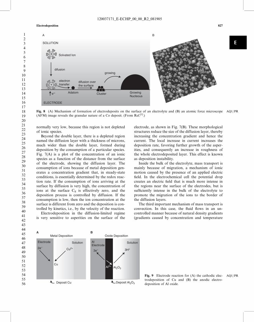
normally very low, because this region is not depletedof ionic species.
Beyond the double layer, there is a depleted regionnamed the diffusion layer with a thickness of microns,much wider than the double layer, formed duringdeposition by the consumption of a particular species.Fig. 7(A) is a plot of the concentration of an ionicspecies as a function of the distance from the surfaceof the electrode, showing the diffusion layer. Theconsumption of ions because of metal deposition gen-erates a concentration gradient that, in steady-stateconditions, is essentially determined by the redox reac-tion rate. If the consumption of ions arriving at thesurface by diffusion is very high, the concentration ofions at the surface CS is effectively zero, and thedeposition process is controlled by diffusion. If theconsumption is low, then the ion concentration at thesurface is different from zero and the deposition is con-trolled by kinetics, i.e., by the velocity of the reaction.
Electrodeposition in the diffusion-limited regimeis very sensitive to asperities on the surface of the
electrode, as shown in Fig. 7(B). These morphologicalstructures reduce the size of the diffusion layer, therebyincreasing the concentration gradient and hence thecurrent. The local increase in current increases thedeposition rate, favoring further growth of the asper-ities, and consequently an increase in roughness ofthe whole electrodeposited layer. This effect is knownas deposition instability.
Inside the bulk of the electrolyte, mass transport ismainly because of migration, a mechanism of ionicmotion caused by the presence of an applied electricfield. In the electrochemical cell the potential dropcreates an electric field that is much more intense inthe regions near the surface of the electrodes, but issufficiently intense in the bulk of the electrolyte topromote the migration of the ions to the border ofthe diffusion layers.
The third important mechanism of mass transport isconvection. In this case, the fluid flows in an un-controlled manner because of natural density gradients(gradients caused by concentration and temperature
++ +
+ +
++
++
++
++
++ +
+ +
++
++
++
++
SOLUTION
Solvated Ion
difusion
electrontransfer
difusion overthe surface
growing
GrowingNucleous
ClusterAdatome–
ELECTRODE
A B
Fig. 8 (A) Mechanism of formation of electrodeposits on the surface of an electrolyte and (B) an AQ1=PRatomic force microscope(AFM) image reveals the granular nature of a Co deposit. (From Ref.[1].)
Metal DepositionA B
Oxide Deposition
ElectrodeElectrode
Solution Solution
Deposit Cu Deposit Al2O3
Al2O3
Cu
Al
Cu2+
Al3+
3H+3e–
2e–
Fig. 9 Electrode reaction AQ1=PRfor (A) the cathodic elec-trodeposition of Cu and (B) the anodic electro-
deposition of Al oxide.
Electrodeposition 827
E
123456789
1011121314151617181920212223242526272829303132333435363738394041424344454647484950515253545556
120037171_E-ECHP_00_00_R2_081905
fluctuations). Convection can also be produced in acontrolled manner by different methods, such asmechanically stirring the electrolyte.
Growth Mechanisms
To complete the explanation about the mechanisms ofelectrodeposition, it is very important to give an ideaabout the formation of the deposits. A model for theelectrodeposition process considers a solvated ion goingthrough the diffusion layer as a first step, looseningof the solvation sheath by transferring electronswith electrode and being adsorbed (adatom) as thesecond step, and surface diffusion and incorporationin an energetically favorable site as the third step.The deposition sites can be punctual or extended sur-face defects, such as vacancies or kinks, known in gen-eral as nucleation sites. The nucleation sites allow theformation of nuclei (islands) that evolve to grains,forming compact deposits that grow on top of the sur-face of the electrode. Fig. 8(A) depicts the mechanismof layer growth and Fig. 8(B) shows an atomic force
microscopy (AFM) image of an electrodeposited layerfrom an electrolyte containing cobalt sulfate. Theimage clearly reveals the formation of Co grains ontop of electrode surface.
Electrode Reactions
The current that flows at the working electrode maybe divided into two kinds: faradaic and non-faradaic.The faradaic processes are the ones where chargesare transferred across the liquid–solid interface. Theseprocesses are called faradaic because they followFaraday’s law, which says the amount of substancethat undergoes oxidation or reduction at each elec-trode is directly proportional to the amount of electri-city that passes through the cell. Two faradaicprocesses that are directly related to electrodepositionare shown in Fig. 9, where Fig. 9(A) represents simplythe deposition of Cu by reduction of Cu2þ and Fig.9(B) the growth of Al anodic oxide by oxidation ofmetallic aluminum, this being an example of anodicelectrodeposition. Non-faradaic processes are struc-
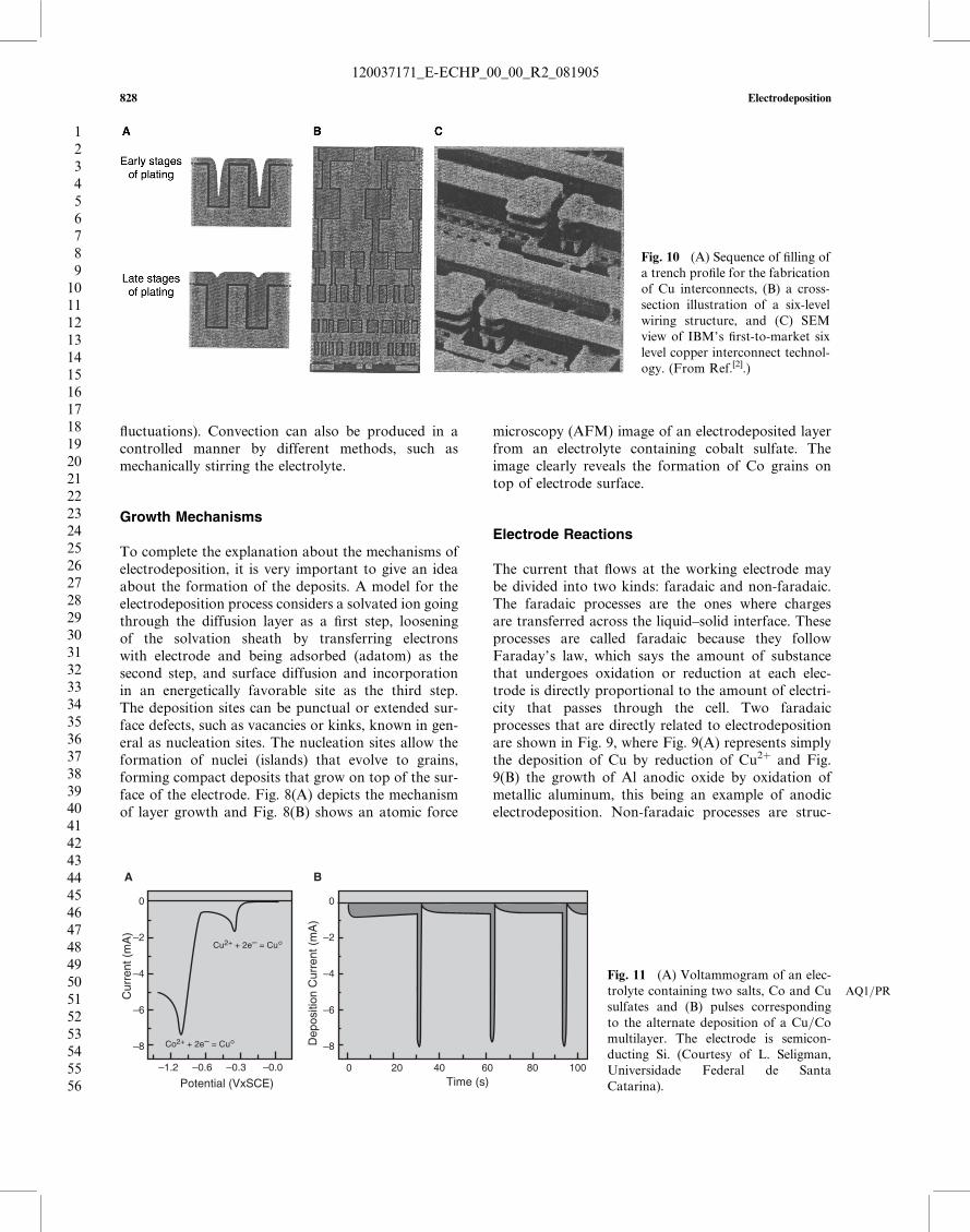
Fig. 10 (A) Sequence of filling ofa trench profile for the fabricationof Cu interconnects, (B) a cross-
section illustration of a six-levelwiring structure, and (C) SEMview of IBM’s first-to-market six
level copper interconnect technol-ogy. (From Ref.[2].)
0
–2
–4
–6
–8
–1.2 –0.6 –0.3 –0.0
0
–2
–4
–6
–8
0 20 40 60 80 100
Potential (VxSCE)
Cur
rent
(m
A)
Time (s)
Dep
ositi
on C
urre
nt (
mA
)
A B
Cu2+ + 2e– = Cu°
Co2+ + 2e– = Cu°
Fig. 11 (A) Voltammogram of an elec-trolyte containing two AQ1=PRsalts, Co and Cusulfates and (B) pulses corresponding
to the alternate deposition of a Cu=Comultilayer. The electrode is semicon-ducting Si. (Courtesy of L. Seligman,Universidade Federal de Santa
Catarina).
828 Electrodeposition
123456789
1011121314151617181920212223242526272829303132333435363738394041424344454647484950515253545556
120037171_E-ECHP_00_00_R2_081905
tural changes of the electrode–solution interface, suchas absorption and desorption of species that changethe potential of the electrode and solution compositionwithout charge transfer.
ELECTRODEPOSITION IN MICROELECTRONICS
Recently, there has been a boom in the use of electro-deposition for microelectronics. The microelectronicsindustry came to the conclusion that the electrodeposi-tion of Cu is the ideal manufacturing process forwiring for semiconductor logic and memory devices.Wiring is the network of wires that interconnects thedevices (transistors) on integrated-circuit chips. Cop-per is a highly conductive metal and is relatively easyto electrodeposit. Since 1997, Cu has been successfullyused for the production of interconnects.[2] Nowadays,such interconnects are electrodeposited in trencheswith widths of 0.13 mm or less. The ability to filltrenches and vials with a plated material is calledsuperfilling and is illustrated in Fig. 10(A). Thecross-section of the device illustrated in Fig. 10(B)depicts the multilevel wiring structure of an integratedcircuit and Fig. 10(C) shows a real arrangement ofelectrodeposited interconnects in a device fabricatedby IBM.
ELECTRODEPOSITION IN NANOSCIENCEAND NANOTECHNOLOGY
Simultaneously, with the rapid growth of electrodepo-sition in microelectronics, a new trend based on theelectrodeposition of materials, structures, particles,devices, etc., generally called nano-objects, withdimensions below 100 nm commenced. Nano-objectsare fundamental for nanoscience investigations andnanotechnology development. A nano-object is ofparticular interest if it has physical properties thatdiffer from objects that have macroscopic sizes.Quantization of energy, for example, is observedin systems with greatly reduced size, such as atoms,molecules, and nanostructures.
Electrodeposition is an elegant and efficient techni-que for the production of nano-objects. Using thepulse deposition mode, it is possible to control theamount of atoms to be deposited with great precision.That is, pulsing with pulse durations of a few millise-conds to a few seconds, allows the deposition ofclusters of atoms or layers with thickness of a few tohundreds of nanometers.
A typical example of an electrodeposited nanostruc-ture is a multilayered structure. By having two salts inthe electrolyte and applying two potentials in alterna-tion, it is possible to deposit multilayer structures,
A B
0.6
0.4
0.2
0.0
–240 –120 0 120 240
AM
R %
Applied Field (Oe)
MR
%
Applied Field (Oe)
–1000 –500 0 500 1000
0
2
4
6
8 Number ofLayers :
91319
Fig. 12 (A) AMR of single AQ1=PRlayer of Co[1] and(B) GMR results depending on the number of
layers. (From Ref.[5].) The substrate is semi-conducting Si.
Time (s)
Cur
rent
(m
A)
–4
–5
–6
–7
–8
10 20 30 40
A
Fig. 13 (A) Spontaneous AQ1=PRcurrent
oscillations during deposition atconstant applied potential usingan electrolyte containing Cu
sulfate and lactic acid (Courtesyof R.G. Delatorre, UniversidadeFederal de Santa Catarina) and
(B) SEM image of Cu=Cu2O mul-tilayered wires. (From Ref.[8].)
Electrodeposition 829
E
123456789
1011121314151617181920212223242526272829303132333435363738394041424344454647484950515253545556
120037171_E-ECHP_00_00_R2_081905
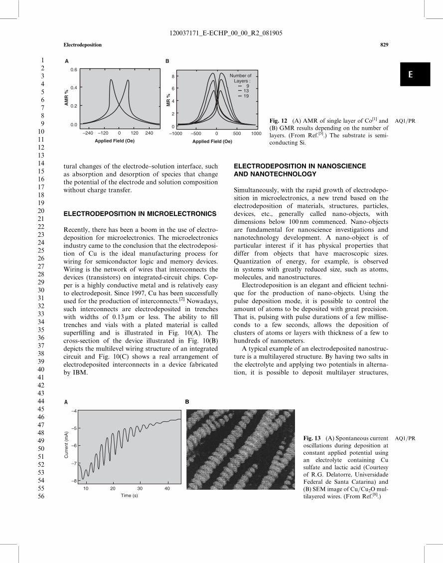
which are artificially fabricated materials that haveapplication in the electronics industry. Fig. 11(A)shows the polarization curve for an electrolyte contain-ing two salts, CuSO4 and CoSO4, where the reductionpeaks of each metal are clearly seen. Pulsing the cath-odic potential rapidly between a value at which only Cuis reduced, and one at which a Co-rich alloy is reduced,generates a deposit that is a Cu=Co multilayer withindividual layers of nanometric thickness. The layerthickness may be controlled by integrating the currentin real time and calculating the electrodeposited chargeor, more simply, by controlling the deposition time.Fig. 11(B) shows typical current transients with charac-teristic peaks for each layer electrodeposited. The Codeposition current is much higher than the Cu onebecause to assure the deposition of a Co-rich alloythe concentration of Co sulfate in the electrolyte hasto be much higher than the Cu sulfate concentration.
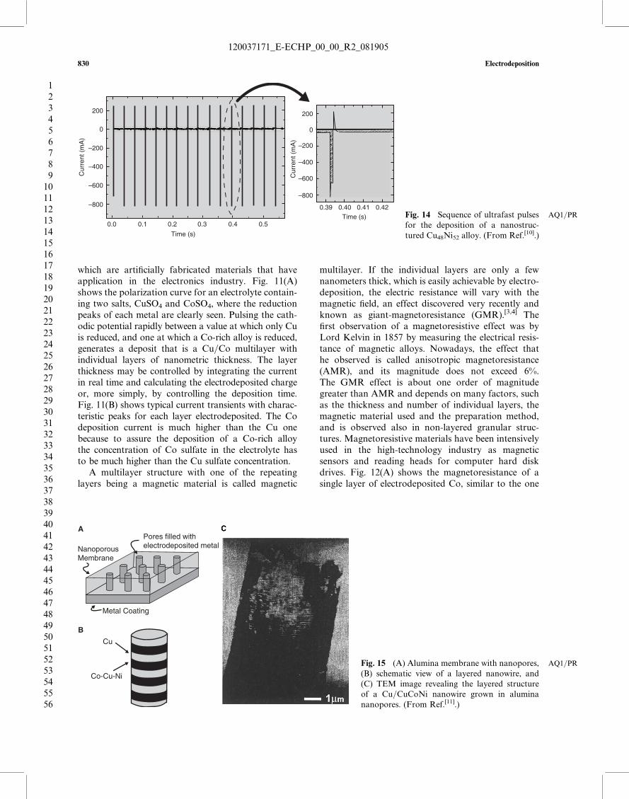
A multilayer structure with one of the repeatinglayers being a magnetic material is called magnetic
multilayer. If the individual layers are only a fewnanometers thick, which is easily achievable by electro-deposition, the electric resistance will vary with themagnetic field, an effect discovered very recently andknown as giant-magnetoresistance (GMR).[3,4] Thefirst observation of a magnetoresistive effect was byLord Kelvin in 1857 by measuring the electrical resis-tance of magnetic alloys. Nowadays, the effect thathe observed is called anisotropic magnetoresistance(AMR), and its magnitude does not exceed 6%.The GMR effect is about one order of magnitudegreater than AMR and depends on many factors, suchas the thickness and number of individual layers, themagnetic material used and the preparation method,and is observed also in non-layered granular struc-tures. Magnetoresistive materials have been intensivelyused in the high-technology industry as magneticsensors and reading heads for computer hard diskdrives. Fig. 12(A) shows the magnetoresistance of asingle layer of electrodeposited Co, similar to the one
Cur
rent
(m
A)
200
0
–200
–400
–600
–800
0.0 0.1 0.2 0.3 0.4 0.5
Time (s)
200
0
–200
–400
–600
–800
Cur
rent
(m
A)
0.39 0.40 0.41 0.42Time (s) Fig. 14 Sequence AQ1=PRof ultrafast pulses
for the deposition of a nanostruc-
tured Cu48Ni52 alloy. (From Ref.[10].)
Cu
Co-Cu-Ni
Metal Coating
NanoporousMembrane
Pores filled withelectrodeposited metal
A
B
Fig. 15 (A) Alumina AQ1=PRmembrane with nanopores,
(B) schematic view of a layered nanowire, and(C) TEM image revealing the layered structureof a Cu=CuCoNi nanowire grown in alumina
nanopores. (From Ref.[11].)
830 Electrodeposition
123456789
1011121314151617181920212223242526272829303132333435363738394041424344454647484950515253545556
120037171_E-ECHP_00_00_R2_081905
depicted in Fig. 5, which shows an AMR effect of0.5%. Fig. 12(B) illustrates the case of a magnetic mul-tilayer, also electrodeposited, with the effect dependingon the number of layers, reaching in this case amaximum of 8.5% for 15 Co=Cu layers.
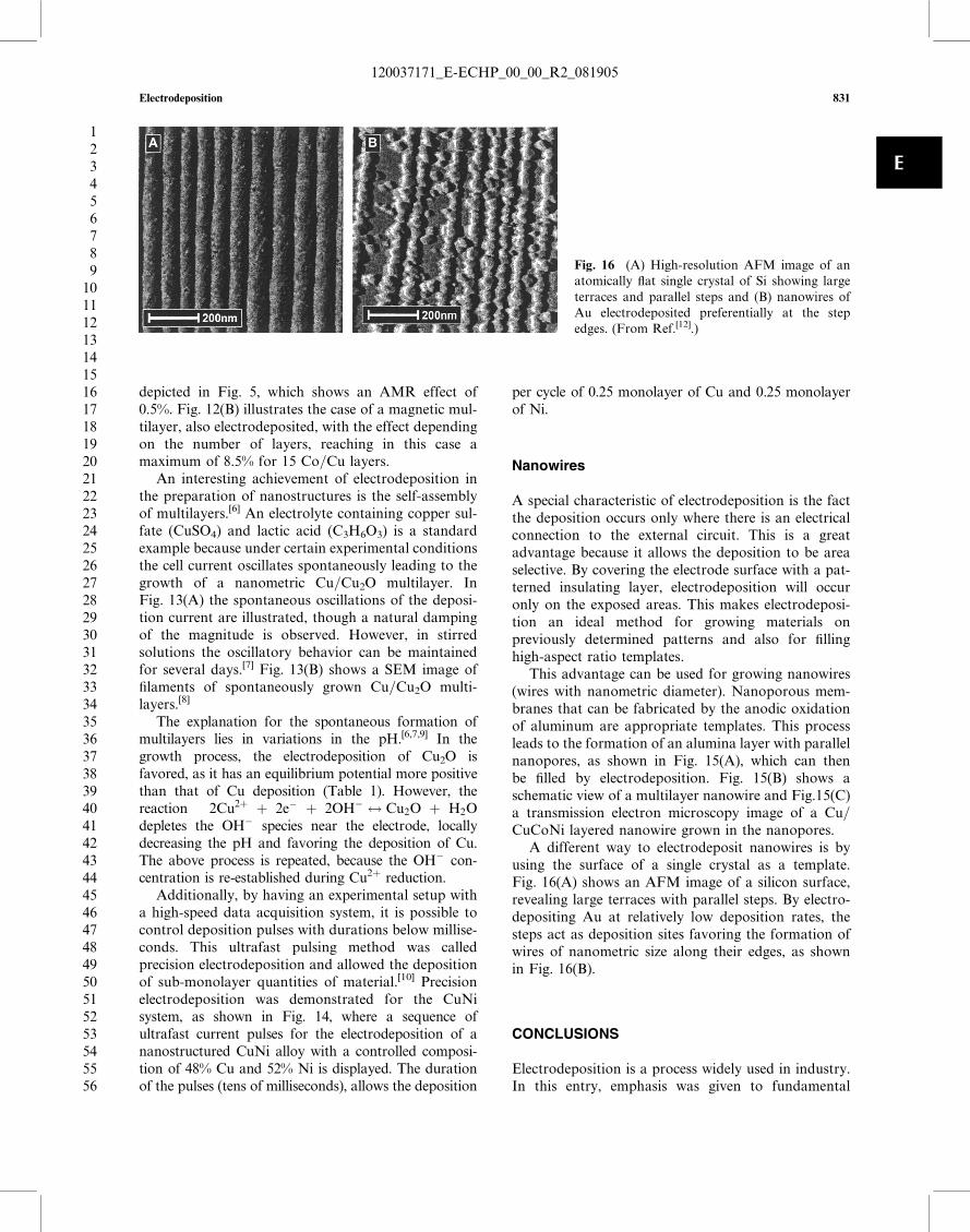
An interesting achievement of electrodeposition inthe preparation of nanostructures is the self-assemblyof multilayers.[6] An electrolyte containing copper sul-fate (CuSO4) and lactic acid (C3H6O3) is a standardexample because under certain experimental conditionsthe cell current oscillates spontaneously leading to thegrowth of a nanometric Cu=Cu2O multilayer. InFig. 13(A) the spontaneous oscillations of the deposi-tion current are illustrated, though a natural dampingof the magnitude is observed. However, in stirredsolutions the oscillatory behavior can be maintainedfor several days.[7] Fig. 13(B) shows a SEM image offilaments of spontaneously grown Cu=Cu2O multi-layers.[8]
The explanation for the spontaneous formation ofmultilayers lies in variations in the pH.[6,7,9] In thegrowth process, the electrodeposition of Cu2O isfavored, as it has an equilibrium potential more positivethan that of Cu deposition (Table 1). However, thereaction 2Cu2þ þ 2e� þ 2OH� $ Cu2O þ H2Odepletes the OH� species near the electrode, locallydecreasing the pH and favoring the deposition of Cu.The above process is repeated, because the OH� con-centration is re-established during Cu2þ reduction.
Additionally, by having an experimental setup witha high-speed data acquisition system, it is possible tocontrol deposition pulses with durations below millise-conds. This ultrafast pulsing method was calledprecision electrodeposition and allowed the depositionof sub-monolayer quantities of material.[10] Precisionelectrodeposition was demonstrated for the CuNisystem, as shown in Fig. 14, where a sequence ofultrafast current pulses for the electrodeposition of ananostructured CuNi alloy with a controlled composi-tion of 48% Cu and 52% Ni is displayed. The durationof the pulses (tens of milliseconds), allows the deposition
per cycle of 0.25 monolayer of Cu and 0.25 monolayerof Ni.
Nanowires
A special characteristic of electrodeposition is the factthe deposition occurs only where there is an electricalconnection to the external circuit. This is a greatadvantage because it allows the deposition to be areaselective. By covering the electrode surface with a pat-terned insulating layer, electrodeposition will occuronly on the exposed areas. This makes electrodeposi-tion an ideal method for growing materials onpreviously determined patterns and also for fillinghigh-aspect ratio templates.
This advantage can be used for growing nanowires(wires with nanometric diameter). Nanoporous mem-branes that can be fabricated by the anodic oxidationof aluminum are appropriate templates. This processleads to the formation of an alumina layer with parallelnanopores, as shown in Fig. 15(A), which can thenbe filled by electrodeposition. Fig. 15(B) shows aschematic view of a multilayer nanowire and Fig.15(C)a transmission electron microscopy image of a Cu=CuCoNi layered nanowire grown in the nanopores.
A different way to electrodeposit nanowires is byusing the surface of a single crystal as a template.Fig. 16(A) shows an AFM image of a silicon surface,revealing large terraces with parallel steps. By electro-depositing Au at relatively low deposition rates, thesteps act as deposition sites favoring the formation ofwires of nanometric size along their edges, as shownin Fig. 16(B).
CONCLUSIONS
Electrodeposition is a process widely used in industry.In this entry, emphasis was given to fundamental
Fig. 16 (A) High-resolution AFM image of anatomically flat single crystal of Si showing large
terraces and parallel steps and (B) nanowires ofAu electrodeposited preferentially at the stepedges. (From Ref.[12].)
Electrodeposition 831
E
123456789
1011121314151617181920212223242526272829303132333435363738394041424344454647484950515253545556
120037171_E-ECHP_00_00_R2_081905
aspects and to future potential applications of thistechnique.
ACKNOWLEDGMENT
The authors wish to thank Prof. Walther Schwarzacherfrom Bristol University for reading carefully the manu-script and the Brazalian agencies CAPES, CNPQ, andFAPESC.
REFERENCES
1. Munford, M.L.; Sartorelli, M.L.; Seligman, L.;Pasa, A.A. Morphology and magnetic propertiesof Co thin films electrodeposited on Si. J. Electro-chem. Soc. 2002, 149 (5), C274–C279.
2. Andricacos, P.C. Copper on-chip interconnec-tions: a breakthrough in electrodeposition tomake better chips. Interface (Electrochem. Soc.)1999, 8, 33–48.
3. Baibich, M.N.; Broto, J.M.; Fert, A.; Nguyen VanDau, F.; Petroff, F.; Eitenne, P.; Creuzet, G.;Friederich, A.; Chazelas, J. Giant magnetoresis-tance of (001)Fe=(001)Cr magnetic superlattices.Phys. Rev. Lett. 1988, 61, 2472–2475.
4. Binasch, G.; Grunberg, P.; Saurenbach, F.; Zinn,W. Enhanced magnetoresistance in layered mag-netic structures with antiferromagnetic interlayerexchange. Phys. Rev. B. 1989, 39, 4828–4830.
5. Seligman, L.; Sartorelli, M.L.; Pasa, A.A.;Schwarzacher, W.; Kasyutich, O.I. Co=Cu spinvalves electrodeposited on Si. J. Magn. Magn.Mater. 2001, 226, 752–753.
6. Switzer, J.A.; Hung, C.J.; Huang, L.Y.; Miller,F.S.; Zhou, Y.C.; Raub, E.R.; Shumsky, M.G.;Bohannan, E.W. Potential oscillations duringthe electrochemical self-assembly of copper
cuprous oxide layered nanostructures. J. Mater.Res. 1998, 13 (4), 909–916.
7. Switzer, J.A.; Hung, C.-J.; Huang, L.-Y.; Switzer,E.R.; Kammler, D.R.; Golden, T.D.; Bohannan,E.W. Electrochemical self-assembly of copper=cuprous oxide layered nanostructures. J. Am.Chem. Soc. 1998, 120, 3530–3531.
8. Wang, M.; Zhong, S.; Yin, X.-B.; Zhu, J.-M.;Peng, R.-W.; Wang, Y.; Zhang, K.-Q.; Ming, N.-B.Nanostructured copper filaments in electroche-mical deposition. Phys. Rev. Lett. 2001, 86, 3827–3830.
9. Zhang, M.-Z.; Wang, M.; Zhang, Z.; Zhu, J.-M.;Peng, R.-W.; Ming, N.-B. Periodic structures ofrandomly distributed Cu=Cu2O nanograins andperiodic variations of cell voltage in copper elec-trodeposition. Electrochim. Acta 2004, 49 (14),2379–2383.
10. Kazeminezhad, I.; Blythe, H.J.; Schwarzacher, W.Alloys by precision electrodeposition. Appl. Phys.Lett. 2001, 78 (7), 1014–1016.
11. Schwarzacher, W. Metal nanostructures: a newclass of electronic devices. Interface (Electrochem.Soc.) 1999, 8, 20–24.
12. Munford, M.L.; Maroun, F.; Cortes, R.;Allongue, P.; Pasa, A.A. Electrochemical growthof gold on well-defined vicinal H–Si(1 1 1) sur-faces studied by AFM and XRD. Surf. Sci.2003, 537 (1–3), 95–112.
FURTHER READINGS
Brad, A.J.; Faulkner, L.R. Electrochemical Methods:Fundamentals and Applications; Wiley: New York,1980.
Schlesinger, M., Paunovic, M., Eds.; ModernElectroplating, 4th Ed.; Wiley: New York, 2000.
832 Electrodeposition
123456789
1011121314151617181920212223242526272829303132333435363738394041424344454647484950515253545556
120037171_E-ECHP_00_00_R2_081905