Embed Size (px)
Citation preview
IOP PUBLISHING NANOTECHNOLOGY
Nanotechnology 19 (2008) 325711 (7pp) doi:10.1088/0957-4484/19/32/325711
Synthesis and characterization ofcadmium telluride nanowireMaxwell C Kum1, Bong Young Yoo2, Young Woo Rheem1,Krassimir N Bozhilov3, Wilfred Chen1, Ashok Mulchandani1,4 andNosang V Myung1,4
1 Department of Chemical and Environmental Engineering and Center for Nanoscale Scienceand Engineering, University of California, Riverside, CA 92521, USA2 Division of Materials and Chemical Engineering, Hanyang University, Ansan 426-791,Korea3 Central Facility for Advanced Microscopy and Microanalysis, University of California,Riverside, CA 92521, USA
E-mail: [email protected] and [email protected]
Received 9 May 2008, in final form 6 June 2008Published 4 July 2008Online at stacks.iop.org/Nano/19/325711
AbstractCdTe nanowires with controlled composition were cathodically electrodeposited usingtrack-etched polycarbonate membrane as scaffolds and their material and electrical propertieswere systematically investigated. As-deposited CdTe nanowires show nanocrystalline cubicphase structures with grain sizes of up to 60 nm. The dark-field images of nanowires reveal thatthe crystallinity of nanowires was greatly improved from nanocrystalline to a few single crystalswithin nanowires upon annealing at 200 ◦C for 6 h in a reducing environment(5% H2 + 95% N2). For electrical characterization, a single CdTe nanowire was assembledacross microfabricated gold electrodes using the drop-casting method. In addition to an increasein grain size, the electrical resistivity of an annealed single nanowire (a few 105 � cm) was oneorder of magnitude greater than in an as-deposited nanowire, indicating that crystallinity ofnanowires improved and defects within nanowires were reduced during annealing. Bycontrolling the dopants levels (e.g. Te content of nanowires), the resistivity of nanowires wasvaried from 104 to 100 � cm. Current–voltage (I –V ) characteristics of nanowires indicated thepresence of Schottky barriers at both ends of the Au/CdTe interface. Temperature-dependentI –V measurements show that the electron transport mode was determined by a thermallyactivated component at T > −50 ◦C and a temperature-independent component below −50 ◦C.Under optical illumination, the single CdTe nanowire exhibited enhanced conductance.
1. Introduction
Cadmium telluride (CdTe) is a II–VI semiconductor that hasbeen widely used for a variety of applications. The directbandgap of 1.44 eV at room temperature and the high opticalabsorption coefficient [1] in the visible spectrum make CdTe anideal material for photovoltaics. Bandgap engineering of CdTe,in the form of Cd1−x ZnxTe and Hg1−x Cdx Te, also providesexciting research opportunities in the field of x-ray, gamma-ray and infrared detectors [2, 3]. In addition, innovativeresearch involving nanoscaled CdTe materials, including zero-and one-dimensional, has been investigated intensively over
4 Authors to whom any correspondence should be addressed.
the past few years. By controlling the diameter of thenanoparticle down to a few nanometers, CdTe nanoparticlesoffer a wide range of bandgap energy in the visible spectrumdue to the quantum confinement effect [4, 5]. Since otherone-dimensional cadmium chalcogenide-based nanomaterialssuch as CdS and CdSe have been shown to possess uniqueoptical and electrical properties for nanoscale electronic,optoelectronic and sensor applications [6, 7], one-dimensionalCdTe nanowires have also received a great deal of attention forthese potential exploitations.
Several techniques have been developed to synthesizeCdTe nanowires, including solution-based chemical synthe-sis [8, 9] and self-assembly from CdTe nanoparticles [10], aswell as template-directed electrodeposition [11–14]. Template-
0957-4484/08/325711+07$30.00 © 2008 IOP Publishing Ltd Printed in the UK1
Nanotechnology 19 (2008) 325711 M C Kum et al
directed electrodeposition is regarded as an efficient methodin the synthesis of one-dimensional nanowires because of theease of controlling the dimension of the nanowires. Addi-tionally, low cost and the ability to ‘tailor-make’ propertiesby controlling deposition conditions favor electrodeposition asan attractive synthesis method. Our group has demonstratedthe successful implementation of this technique to fabricatemetallic [15], semiconductor [16] and conducting polymer [17]nanowires. Xu et al [11] first reported the template-directedelectrodeposition of CdTe nanowires in a porous anodized alu-minum oxide (AAO) template from a non-aqueous electrolytebath at a temperature of 160 ◦C. Polycrystalline nanowiresin the hexagonal phase structure were deposited. Using aconventional acidic CdTe thin film electrodeposition bath pio-neered by Panicker et al [18], Zhao et al [12] electrodepositedCdTe nanowires in a porous AAO template at room tempera-ture, and polycrystalline nanowires with cubic phase structurewere synthesized upon annealing. By sputtering a thin layer ofgold on the AAO template after the electrodeposition of CdTenanowires, Ohgai et al [13] measured the electron transportproperties of CdTe nanowire bundles within the AAO template,and concluded that an amorphous phase of CdTe was electrode-posited and that the electron transport was based on a hop-ping conduction mechanism. Sima et al [14] studied the elec-trodeposition of CdTe nanowires in a track-etch polycarbonatemembrane using both acidic and basic baths. Nanowires withhollow tips were obtained with the basic bath and large porediameter polycarbonate membrane.
Although CdTe nanowires have been electrodepositedby a few groups, there have been only a few reportswhich correlate the materials and composition of nanowiresto the electrical and optoelectronic properties of thesenanowires [13], especially for a single CdTe nanowire. Thisaspect of research is critical if a CdTe nanowire is to beintegrated into complex electronic devices. In this work, CdTenanowires with controlled dimension were first synthesizedvia template-directed electrodeposition and the compositionof the nanowires was analyzed as a function of depositionpotential. The effect of crystallinity of the CdTe nanowireon the electrical and optoelectronic properties was examined.Lastly, the electron transport properties of a single CdTenanowire was investigated with temperature-dependent I –Vmeasurements.
2. Experimental methods
The CdTe deposition electrolytes were prepared by dissolvingTeO2 (99.9995%, Alfa Aesar, Inc.) in concentrated sulfuricacid. After the solids were completely dissolved, deionizedH2O and (CdSO4)3·8H2O (Acros Organics) were added toreach the final volume and pH was adjusted by adding H2SO4
and/or NaOH. The final concentration of the bath was 1 MCdSO4 and 0.15 mM TeO2. Deposition temperature was setat 70 ◦C and the bath was magnetically stirred using a 1 inchmagnetic stirring bar at 300 rpm. A 250 ml beaker was used asthe cell with 200 ml of electrolyte.
One side of a track-etched polycarbonate membrane(Whatman) with a normal pore diameter of 30 nm was
sputtered with gold to serve as a seed layer and a workingelectrode was fabricated by adhering the gold-sputtered PCmembrane onto a piece of double-sided adhesive copperconducting tape that was fixed on a glass slide. Ag/AgCland platinum-coated titanium stripe were used as referenceand counter electrode, respectively. Once the electrodepositionwas done, the template was removed from the electrode anddissolved in 1-methyl-2-pyrrolidinone (99.5%, Alfa Aesar,Inc.) overnight at 50 ◦C. The nanowires were then resuspendedin isopropyl alcohol (IPA) and kept in storage for furtherexperiments.
The composition of the CdTe nanowires was determinedvia atomic absorption spectroscopy (AAS, Perkin ElmerAnalyst 800) by first dissolving the nanowires in 1 mlof 35 vol% nitric acid and then further diluted for AASanalysis. X-ray powder diffraction (Bruker D8 advancediffractometer with Cu Kα radiation) was performed whilethe nanowires were still embedded inside the template. Thestructure and crystallinity were characterized by transmissionelectron microscopy (TEM, FEI-Philips CM300) and high-resolution transmission electron microscopy (HRTEM, FEI-Philips CM300) with NW samples that were drop-casted ontocopper grids with a carbon film. Scanning electron microscopy(SEM, Philips XL30 FEG) of nanowires was also taken.
For electrical characterization, CdTe nanowires suspendedin IPA were diluted and sonicated. Dispersed nanowireswere drop-casted onto pre-fabricated 2 μm gap goldmicroelectrodes. Microelectrodes with a single CdTe nanowirebridging across the gold electrodes were saved for furtherexperiments. Electrical measurement at ambient temperatureand pressure was done under the dark using a HewlettPackard 4155A Semiconductor Parameter Analyzer whilethe temperature-dependent electrical measurement was doneunder low pressure and darkness using a Keithley 236 SourceMeasure Unit interfaced with a CTI Cryodyne RefrigerationSystems and 8200 Compressor connected to a Lakeshore 331Temperature Controller. The light source for the photocurrentmeasurement was a laser pointer with a wavelength of 532 nmand output power of 5 mW.
3. Result and discussion
3.1. Electrodeposition of CdTe nanowires
The cathodic electrodeposition mechanism of a CdTe thin filmin acidic medium has been well studied ever since it waspioneered by Panicker et al [18]. It consists of two elementarysteps:
HTeO+2 + 3H+ + 4e− → Te(s) + H2O
E0 = 0.55 V versus NHE (1)
Cd2+ + Te(s) + 2e− → CdTe(s)
E0 = 0.10 V versus NHE. (2)
The first elementary step is the over-potential electrodepo-sition of Te followed by the under-potential deposition (UPD)of Cd2+ onto Te(s) to form CdTe. While the first step isdiffusion-controlled at high over-potential, the second step is
2
Nanotechnology 19 (2008) 325711 M C Kum et al
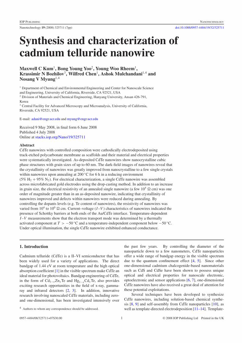
Figure 1. (A) Linear sweep voltammograms (LSV) of CdTeelectrodeposition at (a) pH 1 and (b) pH 2. (B) Dependence of Tecontent on deposition potentials at pH of 1 and 2. The temperaturewas fixed at 70 ◦C. The normal pore size of the polycarbonatemembrane was 30 nm.
kinetic-controlled, independent of the applied potential. If sto-ichiometric CdTe is desired, it is critical to control the rate ofboth steps so that the rate of the second step is either equal toor greater than the rate of the first step. This fundamental con-cept for CdTe thin film electrodeposition has been applied totemplate-directed electrodeposition of CdTe nanowires.
Figure 1(A) is a linear sweep voltammogram (LSV) ofCdTe nanowires’ electrodeposition within a 30 nm pore sizepolycarbonate membrane in an electrolyte containing 1 MCd2+ and 0.15 mM HTeO2
+ at (a) pH 1 and (b) pH 2. TheseLSV curves appeared differently from conventional CdTe thinfilms because the substrate was a polycarbonate membranewith 30 nm size pores and a thickness of 6 μm. Althoughthe bath was magnetically stirred, there was essentially a6 μm diffusion layer between the surface of the poresand the actual gold electrode surface. For pH 1, thefirst cathodic wave between −0.05 V and −0.15 V versusAg/AgCl corresponded to the over-potential electrodepositionof Te(s). The second cathodic wave, between −0.15 V and−0.40 V, and the third cathodic wave, between −0.40 and−0.60 V, represented the under-potential deposition of Cd2+onto Te(s). The difference between the second and the thirdcathodic wave is due to a two-step reaction at the thirdcathodic wave. The third cathodic wave is consistent withobservation from a few reports on a cyclic voltammogram
study of tellurium electrodeposition [19, 20] and it was alsoconfirmed by our group previously [21]. Martın-Gonzaleset al [20] proposed that this cathodic wave was attributedto a two-step reaction involving electrochemical reduction ofHTeO2
+ to H2Te (equation (3)) and chemical deposition of Te(equation (4)):
HTeO2+ + 5H+ + 6e− → H2Te(aq) + 2H2O
E0 = 0.121 V versus NHE (3)
2H2Te + HTeO2+ → 3Te(s) + 2H2O + H+
G0f = −498.118 kJ mol−1. (4)
This two-step reaction was not observed at pH 2 due to thelack of a third cathodic wave since the limiting current densityremained stable from −0.20 V to −0.64 V versus Ag/AgCl.While both Martın-Gonzales et al [20] and Xiao et al [21]added 1 M HNO3 to their deposition bath giving a pH of 0,Traore et al [19] adjusted their bath to a pH of 1 with HClO4.Together with our LSVs at both pH 1 and pH 2, the lack ofthis third cathodic wave in the pH 2 bath seems to indicatethat the reduction of HTeO2
+ (equation (3)) is unfavorableat pH 2. Once the deposition potential was applied beyondbeing more negative than −0.60 V versus Ag/AgCl, the over-potential electrodeposition of cadmium occurred which led toCd-rich CdTe nanowires:
Cd2+ + 2e− → Cd(s) E0 = −0.40 V versus NHE. (5)
The difference of limiting current between pH 1 and pH 2is possibly due to the pore diffusion effect. LSV at pH 1 andpH 2 using a flat plate gold electrode as the substrate in thesame deposition bath showed no such differences in limitedcurrent (data not shown), and no third cathodic wave wasobserved at either pH. In these experiments, the substrate wasthe only difference. One possible explanation for the differencein limiting current is that, with the presence of pore diffusion,the pore diffusion of HTeO+
2 ions was affected by pH since thedeposition of Te(s) and the limited current density is diffusion-limited, while the absence of a cathodic wave representing thereduction of HTeO+
2 (equation (3)) with a flat substrate butdetectable in a porous substrate hints that pore diffusion favorsthe formation of H2Te (equation (3)) only under the conditionof low pH of 1.
By varying the deposition potential and pH of thedeposition bath, the composition of CdTe nanowires wascontrolled. The deposition rate of CdTe nanowires wasestimated at 0.85 μm h−1. At a deposition potential of−0.60 V, near-stoichiometric CdTe nanowires were produced.
3.2. Material characterization
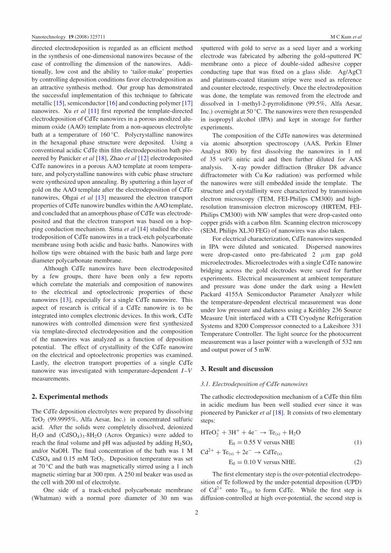
The crystal structure and orientation of CdTe nanowiresas a function of deposition potentials, pH and operatingtemperature were fixed at 2 and 70 ◦C, respectively, andwere examined using x-ray diffraction patterns. Thedeposition potential was varied from −0.575 to −0.625 Vto produce slightly Te-rich to Cd-rich CdTe nanowires.Near-stoichiometric CdTe nanowires were electrodeposited at−0.600 V. As shown in figure 2(A), three diffraction peaks
3
Nanotechnology 19 (2008) 325711 M C Kum et al
Figure 2. X-ray diffraction patterns of electrodeposited (A) CdTenanowires using a 30 nm pore size PC membrane as scaffolds atvarious deposition potentials versus Ag/AgCl at 70 ◦C and (B) CdTenanowires using an 80 nm pore size PC membrane at −0.550 Vversus Ag/AgCl. The deposition temperature was varied from roomtemperature to 70 ◦C.
which correspond to the (111), (220) and (311) indices ofthe cubic phase structure of CdTe (JCPDS: 15-0770) wereobserved. Because the nanowires were oriented verticallywithin the polycarbonate membrane during the XRD scans,the decreasing relative intensity of the (111) peak as theapplied deposition potential becomes more negative suggeststhat the preferential growth orientation was affected by thedeposition potential. The effects of deposition temperatureon the crystal structure and orientation were investigated bydepositing at 70 ◦C and room temperature (figure 2(B)). Asshown in figure 2(B), electrodeposited nanowires from roomtemperature resulted in amorphous nanowires whereas a higherdeposition temperature (70 ◦C) resulting in nanocrystallinenanowires which concur with Panicker et al’s [18] finding onCdTe thin films that higher deposition temperature increasesthe crystallinity of CdTe.
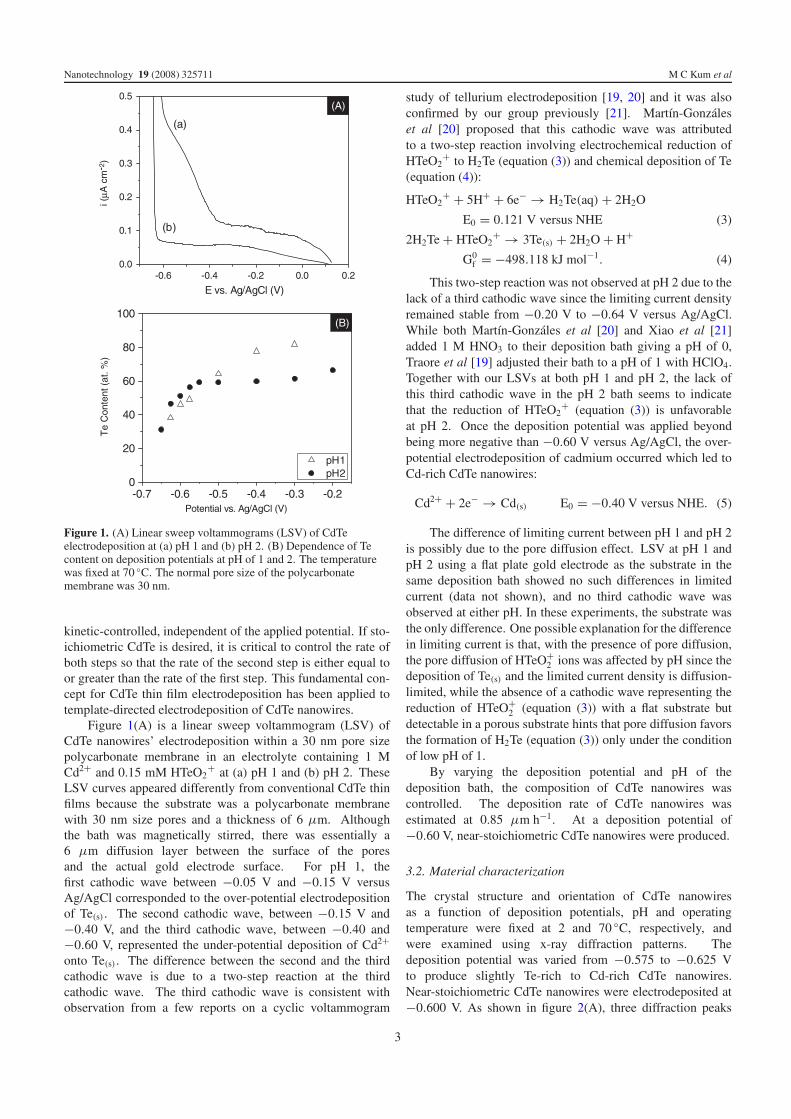
In order to further investigate the morphology and crystalstructure of nanowires, transmission electron microscopy(TEM) and high-resolution transmission electron microscopy(HRTEM) were performed. As shown in TEM bright-field images (figures 3(a) and (d)), the diameter of theelectrodeposited CdTe nanowire was approximately 90 nm.The difference between nanowire diameter and the pore sizeof the polycarbonate membrane occurs because the pores arenot perfect cylindrical with a constant diameter as illustratedby Schonenberger et al [22]. The dark-field image of as-deposited CdTe nanowires (figure 3(b)) indicated that the grainsize ranged from 5 nm up to 60 nm. Selected-area electrondiffraction patterns (SAED) reveal several ring structuresindicating a polycrystallinity of the nanowire (figure 3(c)).The calculated d-spacings from the rings were 3.7, 2.3 and1.95 A, which correspond to the (111), (220) and (311) indices,confirming the earlier XRD results. In order to improve
–
Figure 3. Bright-field ((a), (d)) and dark-field ((b), (e)) TEM images and selected-area diffraction patterns (SAED) of as-deposited((a), (b), (c)) and annealed ((d), (e), (f)) CdTe nanowires. The annealing was performed at 200 ◦C for 6 h.
4
Nanotechnology 19 (2008) 325711 M C Kum et al
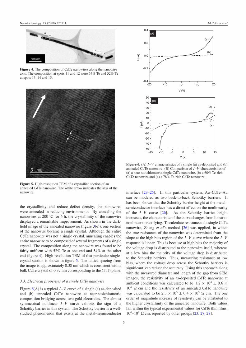
Figure 4. The composition of CdTe nanowires along the nanowireaxis. The composition at spots 11 and 12 were 54% Te and 52% Teat spots 13, 14 and 15.
0.38nm
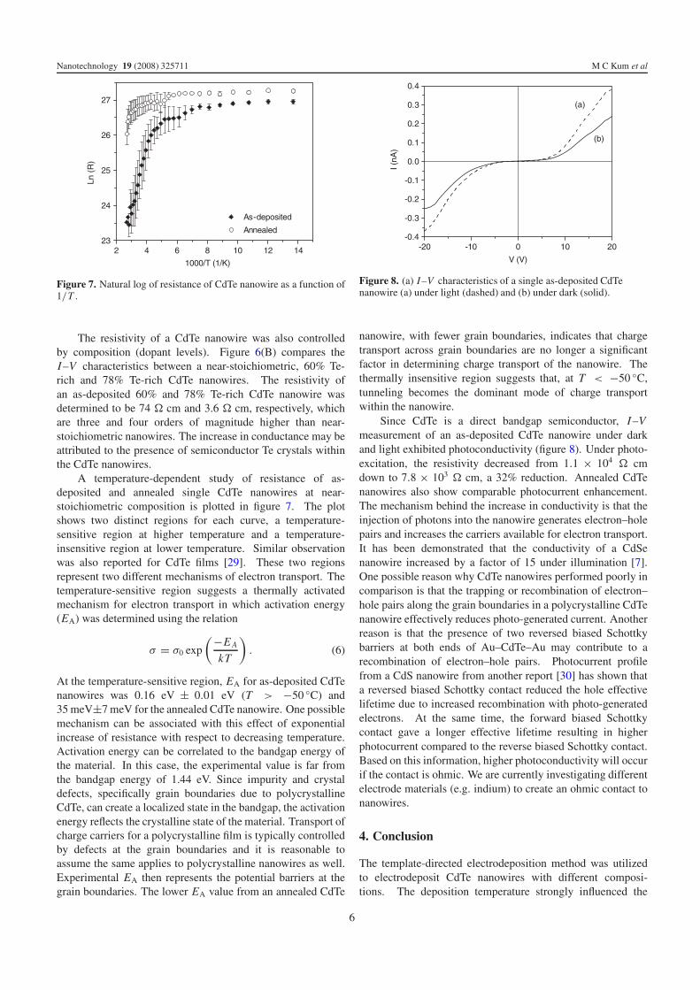
Figure 5. High-resolution TEM of a crystalline section of anannealed CdTe nanowire. The white arrow indicates the axis of thenanowire.
the crystallinity and reduce defect density, the nanowireswere annealed in reducing environments. By annealing thenanowires at 200 ◦C for 6 h, the crystallinity of the nanowiredisplayed a remarkable improvement. As shown in the dark-field image of the annealed nanowire (figure 3(e)), one sectionof the nanowire became a single crystal. Although the entireCdTe nanowire was not a single crystal, annealing enables theentire nanowire to be composed of several fragments of a singlecrystal. The composition along the nanowire was found to befairly uniform with 52% Te at one end and 54% at the otherend (figure 4). High-resolution TEM of that particular single-crystal section is shown in figure 5. The lattice spacing fromthe image is approximately 0.38 nm which is consistent with abulk CdTe crystal of 0.37 nm corresponding to the (111) plane.
3.3. Electrical properties of a single CdTe nanowire
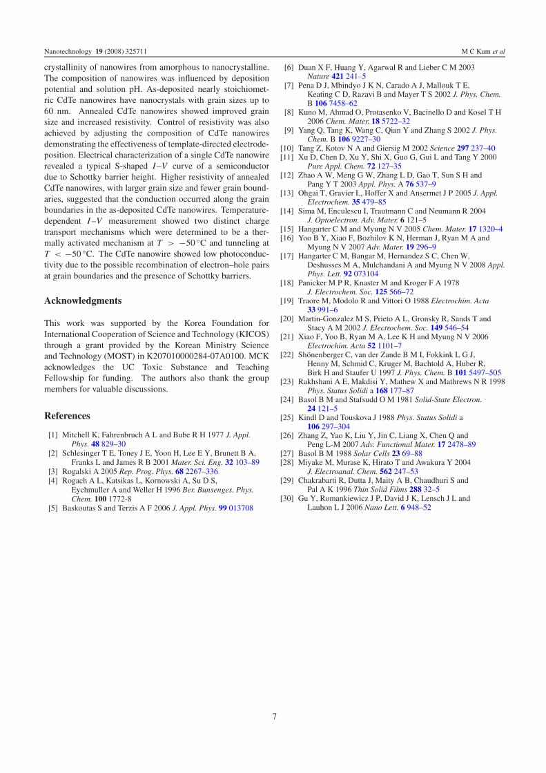
Figure 6(A) is a typical I –V curve of a single (a) as-depositedand (b) annealed CdTe nanowire at near-stoichiometriccomposition bridging across two gold electrodes. The almostsymmetrical nonlinear I –V curve exhibits the sign of aSchottky barrier in this system. The Schottky barrier is a well-studied phenomenon that exists at the metal–semiconductor
Figure 6. (A) I–V characteristics of a single (a) as-deposited and (b)annealed CdTe nanowire. (B) Comparison of I–V characteristics of(a) a near-stoichiometric single CdTe nanowire, (b) a 60% Te-richCdTe nanowire and (c) a 78% Te-rich CdTe nanowire.
interface [23–25]. In this particular system, Au–CdTe–Aucan be modeled as two back-to-back Schottky barriers. Ithas been shown that the Schottky barrier height at the metal–semiconductor interface has a direct effect on the nonlinearityof the I –V curve [26]. As the Schottky barrier heightincreases, the characteristic of the curve changes from linear tononlinear to rectifying. To calculate resistance of a single CdTenanowire, Zhang et al’s method [26] was applied, in whichthe true resistance of the nanowire was determined from theslope at the high bias region of the I –V curve where the I –Vresponse is linear. This is because at high bias the majority ofthe voltage drop is distributed to the nanowire itself, whereasat a low bias the majority of the voltage drop is distributedto the Schottky barriers. Thus, measuring resistance at lowbias, where the voltage drop across the Schottky barriers issignificant, can reduce the accuracy. Using this approach alongwith the measured diameter and length of the gap from SEMimages, the resistivity of an as-deposited CdTe nanowire atambient conditions was calculated to be 1.2 × 10⁴ ± 0.6 ×10⁴ � cm and the resistivity of an annealed CdTe nanowirewas calculated to be 2.3 × 10⁵ ± 0.4 × 10⁵ � cm. The oneorder of magnitude increase of resistivity can be attributed tothe higher crystallinity of the annealed nanowire. Both valuesfall within the typical experimental values for CdTe thin films,104–108 � cm, reported by other groups [23, 27, 28].
5
Nanotechnology 19 (2008) 325711 M C Kum et al
Figure 7. Natural log of resistance of CdTe nanowire as a function of1/T .
The resistivity of a CdTe nanowire was also controlledby composition (dopant levels). Figure 6(B) compares theI –V characteristics between a near-stoichiometric, 60% Te-rich and 78% Te-rich CdTe nanowires. The resistivity ofan as-deposited 60% and 78% Te-rich CdTe nanowire wasdetermined to be 74 � cm and 3.6 � cm, respectively, whichare three and four orders of magnitude higher than near-stoichiometric nanowires. The increase in conductance may beattributed to the presence of semiconductor Te crystals withinthe CdTe nanowires.
A temperature-dependent study of resistance of as-deposited and annealed single CdTe nanowires at near-stoichiometric composition is plotted in figure 7. The plotshows two distinct regions for each curve, a temperature-sensitive region at higher temperature and a temperature-insensitive region at lower temperature. Similar observationwas also reported for CdTe films [29]. These two regionsrepresent two different mechanisms of electron transport. Thetemperature-sensitive region suggests a thermally activatedmechanism for electron transport in which activation energy(EA) was determined using the relation
σ = σ0 exp
(−E A
kT
). (6)
At the temperature-sensitive region, EA for as-deposited CdTenanowires was 0.16 eV ± 0.01 eV (T > −50 ◦C) and35 meV±7 meV for the annealed CdTe nanowire. One possiblemechanism can be associated with this effect of exponentialincrease of resistance with respect to decreasing temperature.Activation energy can be correlated to the bandgap energy ofthe material. In this case, the experimental value is far fromthe bandgap energy of 1.44 eV. Since impurity and crystaldefects, specifically grain boundaries due to polycrystallineCdTe, can create a localized state in the bandgap, the activationenergy reflects the crystalline state of the material. Transport ofcharge carriers for a polycrystalline film is typically controlledby defects at the grain boundaries and it is reasonable toassume the same applies to polycrystalline nanowires as well.Experimental EA then represents the potential barriers at thegrain boundaries. The lower EA value from an annealed CdTe
Figure 8. (a) I–V characteristics of a single as-deposited CdTenanowire (a) under light (dashed) and (b) under dark (solid).
nanowire, with fewer grain boundaries, indicates that chargetransport across grain boundaries are no longer a significantfactor in determining charge transport of the nanowire. Thethermally insensitive region suggests that, at T < −50 ◦C,tunneling becomes the dominant mode of charge transportwithin the nanowire.
Since CdTe is a direct bandgap semiconductor, I –Vmeasurement of an as-deposited CdTe nanowire under darkand light exhibited photoconductivity (figure 8). Under photo-excitation, the resistivity decreased from 1.1 × 10⁴ � cmdown to 7.8 × 10³ � cm, a 32% reduction. Annealed CdTenanowires also show comparable photocurrent enhancement.The mechanism behind the increase in conductivity is that theinjection of photons into the nanowire generates electron–holepairs and increases the carriers available for electron transport.It has been demonstrated that the conductivity of a CdSenanowire increased by a factor of 15 under illumination [7].One possible reason why CdTe nanowires performed poorly incomparison is that the trapping or recombination of electron–hole pairs along the grain boundaries in a polycrystalline CdTenanowire effectively reduces photo-generated current. Anotherreason is that the presence of two reversed biased Schottkybarriers at both ends of Au–CdTe–Au may contribute to arecombination of electron–hole pairs. Photocurrent profilefrom a CdS nanowire from another report [30] has shown thata reversed biased Schottky contact reduced the hole effectivelifetime due to increased recombination with photo-generatedelectrons. At the same time, the forward biased Schottkycontact gave a longer effective lifetime resulting in higherphotocurrent compared to the reverse biased Schottky contact.Based on this information, higher photoconductivity will occurif the contact is ohmic. We are currently investigating differentelectrode materials (e.g. indium) to create an ohmic contact tonanowires.
4. Conclusion
The template-directed electrodeposition method was utilizedto electrodeposit CdTe nanowires with different composi-tions. The deposition temperature strongly influenced the
6
Nanotechnology 19 (2008) 325711 M C Kum et al
crystallinity of nanowires from amorphous to nanocrystalline.The composition of nanowires was influenced by depositionpotential and solution pH. As-deposited nearly stoichiomet-ric CdTe nanowires have nanocrystals with grain sizes up to60 nm. Annealed CdTe nanowires showed improved grainsize and increased resistivity. Control of resistivity was alsoachieved by adjusting the composition of CdTe nanowiresdemonstrating the effectiveness of template-directed electrode-position. Electrical characterization of a single CdTe nanowirerevealed a typical S-shaped I –V curve of a semiconductordue to Schottky barrier height. Higher resistivity of annealedCdTe nanowires, with larger grain size and fewer grain bound-aries, suggested that the conduction occurred along the grainboundaries in the as-deposited CdTe nanowires. Temperature-dependent I –V measurement showed two distinct chargetransport mechanisms which were determined to be a ther-mally activated mechanism at T > −50 ◦C and tunneling atT < −50 ◦C. The CdTe nanowire showed low photoconduc-tivity due to the possible recombination of electron–hole pairsat grain boundaries and the presence of Schottky barriers.
Acknowledgments
This work was supported by the Korea Foundation forInternational Cooperation of Science and Technology (KICOS)through a grant provided by the Korean Ministry Scienceand Technology (MOST) in K207010000284-07A0100. MCKacknowledges the UC Toxic Substance and TeachingFellowship for funding. The authors also thank the groupmembers for valuable discussions.
References
[1] Mitchell K, Fahrenbruch A L and Bube R H 1977 J. Appl.Phys. 48 829–30
[2] Schlesinger T E, Toney J E, Yoon H, Lee E Y, Brunett B A,Franks L and James R B 2001 Mater. Sci. Eng. 32 103–89
[3] Rogalski A 2005 Rep. Prog. Phys. 68 2267–336[4] Rogach A L, Katsikas L, Kornowski A, Su D S,
Eychmuller A and Weller H 1996 Ber. Bunsenges. Phys.Chem. 100 1772-8
[5] Baskoutas S and Terzis A F 2006 J. Appl. Phys. 99 013708
[6] Duan X F, Huang Y, Agarwal R and Lieber C M 2003Nature 421 241–5
[7] Pena D J, Mbindyo J K N, Carado A J, Mallouk T E,Keating C D, Razavi B and Mayer T S 2002 J. Phys. Chem.B 106 7458–62
[8] Kuno M, Ahmad O, Protasenko V, Bacinello D and Kosel T H2006 Chem. Mater. 18 5722–32
[9] Yang Q, Tang K, Wang C, Qian Y and Zhang S 2002 J. Phys.Chem. B 106 9227–30
[10] Tang Z, Kotov N A and Giersig M 2002 Science 297 237–40[11] Xu D, Chen D, Xu Y, Shi X, Guo G, Gui L and Tang Y 2000
Pure Appl. Chem. 72 127–35[12] Zhao A W, Meng G W, Zhang L D, Gao T, Sun S H and
Pang Y T 2003 Appl. Phys. A 76 537–9[13] Ohgai T, Gravier L, Hoffer X and Ansermet J P 2005 J. Appl.
Electrochem. 35 479–85[14] Sima M, Enculescu I, Trautmann C and Neumann R 2004
J. Optoelectron. Adv. Mater. 6 121–5[15] Hangarter C M and Myung N V 2005 Chem. Mater. 17 1320–4[16] Yoo B Y, Xiao F, Bozhilov K N, Herman J, Ryan M A and
Myung N V 2007 Adv. Mater. 19 296–9[17] Hangarter C M, Bangar M, Hernandez S C, Chen W,
Deshusses M A, Mulchandani A and Myung N V 2008 Appl.Phys. Lett. 92 073104
[18] Panicker M P R, Knaster M and Kroger F A 1978J. Electrochem. Soc. 125 566–72
[19] Traore M, Modolo R and Vittori O 1988 Electrochim. Acta33 991–6
[20] Martin-Gonzalez M S, Prieto A L, Gronsky R, Sands T andStacy A M 2002 J. Electrochem. Soc. 149 546–54
[21] Xiao F, Yoo B, Ryan M A, Lee K H and Myung N V 2006Electrochim. Acta 52 1101–7
[22] Shonenberger C, van der Zande B M I, Fokkink L G J,Henny M, Schmid C, Kruger M, Bachtold A, Huber R,Birk H and Staufer U 1997 J. Phys. Chem. B 101 5497–505
[23] Rakhshani A E, Makdisi Y, Mathew X and Mathrews N R 1998Phys. Status Solidi a 168 177–87
[24] Basol B M and Stafsudd O M 1981 Solid-State Electron.24 121–5
[25] Kindl D and Touskova J 1988 Phys. Status Solidi a106 297–304
[26] Zhang Z, Yao K, Liu Y, Jin C, Liang X, Chen Q andPeng L-M 2007 Adv. Functional Mater. 17 2478–89
[27] Basol B M 1988 Solar Cells 23 69–88[28] Miyake M, Murase K, Hirato T and Awakura Y 2004
J. Electroanal. Chem. 562 247–53[29] Chakrabarti R, Dutta J, Maity A B, Chaudhuri S and
Pal A K 1996 Thin Solid Films 288 32–5[30] Gu Y, Romankiewicz J P, David J K, Lensch J L and
Lauhon L J 2006 Nano Lett. 6 948–52
7


![Cadmium Zinc Telluride Solar Cells by Close Spaced Sublimation[1]](https://img.pdfslide.us/doc/110x75/54fbeae64a7959434c8b52e3/cadmium-zinc-telluride-solar-cells-by-close-spaced-sublimation1.jpg)

