Embed Size (px)
Citation preview


Learning ObjectivesBe able to describe the basic processes of microfabricationBe able to explain the principles of photolithography.Be able to describe the basic mechanisms of the additive
processes, including relative comparisons among them.Physical Vapor Deposition (evaporation, sputtering)Chemical Vapor Deposition
Be able to describe the basic mechanisms of the subtractive processes, including relative comparisons among them.Wet Etching (isotropic, anisotropic)Dry Etching (physical, chemical, physical-chemical)
Be able to describe the process of bonding and packaging

Silicon ReviewIn a perfect crystal, each of
silicon’s four outer electrons form covalent bonds, resulting in poor electron mobility (i.e. insulating)
Doping silicon with impurities alters electron mobility (i.e. semiconducting)Extra electron (“N-type”, with
phosphorous, for example)Missing electron (“P-type”,
with boron, for example)

Silicon MicromachinesThe other application is
micromachines, also called the microelectricmechanical system (MEMS), which have the potential of making the computer obsolete
The micromachines include:Fuel cellsDNA chips……

MicrofabricationSilicon crystal structure is regular, well-
understood, and to a large extent controllable.It is all about control: the size of a transistor is 1
m, the doping must therefore less than have of that
How to control?

Microfabrication Techniques

Microfabrication Process of Si
Single crystal growing
Waferslicing
Filmdeposition
Oxidation
Diffusion Ionimplantation
Etching Lithography
Metallization Bonding Packaging Testing

Silicon wafer fabrication

Crystal Growing
Silicon occurs naturally in the forms of silicon dioxide and various silicates and hence, must be purified
The process of purifying silicon:Heating to produce 95% ~ 98% pure
polycrystalline siliconUsing Czochralski (CZ) process to
grow single crystal silicon
1 rev/s
10 m/s
Liquid silicon
Illustration of CZ process

Crystal Growing

Czochralski Method
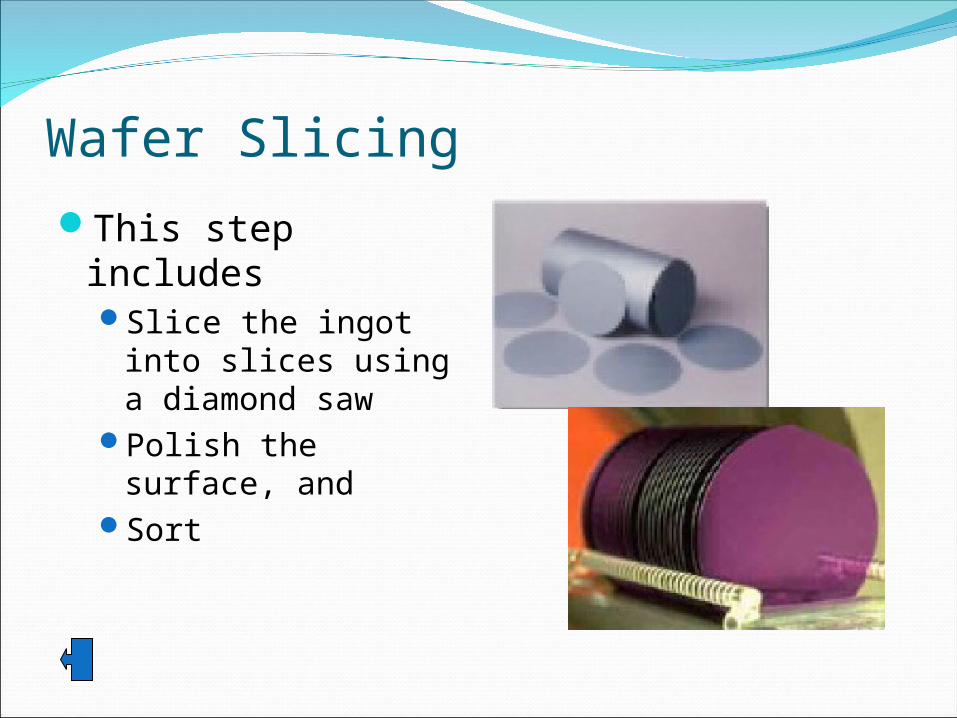
Wafer Slicing
This step includesSlice the ingot into
slices using a diamond saw
Polish the surface, and
Sort

Film Deposits
This step is used to add a special layer on the surface of the silicon for masking
Many types of films are used for insulating / conducting, including polysilicon, silicon nitride, silicon dioxide, tungsten, and titanium.
Films may be deposited using various method, includingEvaporationSputteringChemical Vapor Deposition (CVD)

Film Deposits
The process of CVD(a) Continuous, atmospheric-pressure CVD(b) Low-pressure CVC

Clean wafer
Deposit barrier layer
SiO2, Si3N4, metal
Coat with photoresist
Soft bake
Align masks
Substrate
SiO 2
Substrate
SiO 2
PR
Substrate
SiO 2
PR
Light
Photolithography

Expose pattern
Develop photoresist
Hard bake
Etch windows in
barrier layer
Remove photoresist
Substrate
SiO 2
PR
Substrate
PR
SiO 2
Substrate
SiO 2

PhotolithographySi wafer cleaning procedure
Solvent removalRemoval of residual organic/ionic contaminationHydrous oxide removalHeavy metal clean

Photolithography
Barrier layer formationThe most common material:SiO2
Si3N4, polysilicon, photoresist and metals are used at different points in a process flow
Thermal oxidation, CVD, sputtering and vacuum evaporation

PhotolithographyPhotoresist application
Surface must be clean and dry for adhesionA liquid adhesion promoter is often appliedTo make 2.5 to 0.5 µm thick layer, 1000 to 5000 rpm for 30
to 60 secThe actual thickness viscosity
1/(spinning speed)0.5

PhotolithographyPhotolithography is a process by which an image is optically
transferred from one surface to another, most commonly by the projection of light through a mask onto a photosensitive material.
Photoresist is a material that changes molecular structure when exposed to radiation (e.g. ultraviolet light). It typically consists of a polymer resin, a radiation sensitizer, and a carrier solvent.

Photolithography-spin-coatingAdding a photoresist
layer on the waferA photomask is
typically manifested as a glass plate with a thin metal layer, that is selectively patterned to define opaque and transparent regions.

PhotolithographyPR exposure and development
The photoresist is exposed through the mask with a proper light
The photoresist is developed with a developer supplied by the manufacturer
A positive resist and a negative resist The positive resist yields better process control in small-geometry
structures

Photolithography
A positive photoresist is weakened by radiation exposure, so the remaining pattern after being subject to a developer solution looks just like the opaque regions of the mask
A negative photoresist is strengthened by radiation exposure, so the remaining pattern after being subject to a developer solution appears as the inverse of the opaque regions of the mask.

Wafer aligner and exposure tool

Photolithography-exposureMask alignment
Square glass plate with a patterned emulsion or metal film is placed 25 to 125µm over the wafer
With manual alignment, the wafer is held on a vacuum chuck and carefully moved into position
Computer-controlled alignment equipment achieves high precision alignment
Alignment marks are introduced to align each new mask level to one of the previous levels

UV Exposure Light Source
High pressure mercury arc lamp UV Mercury/Xenon lamp UV Excimer laser (KrF, ArF) DUV (KrF : 248
nm) Electron beams X-ray
Exposed Energy Energy(mJ) = Light intensity(mW) * time(s)
Light Spectrum i line : 365 nm g line : 436 nm h line : 405 nm

Various printing techniques
Lens
Mask
SiO2Photoresist
Wafer Wafer
Wafer
Space
Lens I
Lens II
Mask
SiO2
Photoresist(a) (b)
(c)
(a) Contact printing(b) Proximity printing(c) Projection printing
Ultravioletlight
source

Photolithography-bakingSoft baking (Pre-baking)
To improve adhesion & remove solvent from PR10 to 30min. in an oven at 80 to 90 ºCManufacturer’s data sheets
Hard baking To harden the PR and improve adhesion to the substrate20 to 30 min. at 120 to 180 ºCManufacturer’s data sheets

Photolithography-EtchingEtching techniques
Wet chemical etchingDry etching
Plasma, sputter, RIE, CAIBE, ECR
Photoresist removal Liquid resist strippers cause the resist to swell and lose adhesion
to the substrate Resist ashing: oxidizing(burning) it in an oxygen plasma system

Dry Etching Mechanisms
Physical Removal based on impact &
momentum transfer Poor material selectivity Good directional control High excitation energy Lower pressure, <100 mTorr
Chemical Highest removal rate Good material selectivity Generally isotropic Higher pressure, >100 mTorr
Physical/Chemical Good directional control Intermediate pressure, ~100
mTorr

Isotropic Wet Etching
Etch occurs in all crystallographic directions at the same rate.
Most common formulation is mixture of hydrofluoric, nitric and acetic acids (“HNA”: HF + HNO3 + CH3COOH).
Etch rate may be very fast, many microns per minute.Masks are undercut. High aspect ratio difficult because of diffusion limits.Stirring enhances isotropy.Isotropic wet etching is applicable to many materials besides
silicon
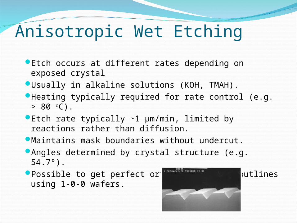
Anisotropic Wet Etching
Etch occurs at different rates depending on exposed crystalUsually in alkaline solutions (KOH, TMAH).Heating typically required for rate control (e.g. > 80 oC).Etch rate typically ~1 µm/min, limited by reactions rather
than diffusion.Maintains mask boundaries without undercut.Angles determined by crystal structure (e.g. 54.7º).Possible to get perfect orthogonal shapes outlines using 1-0-0
wafers.

Etching – a Comparison
ISOTROPIC
Wide variety of materials
No crystal alignment required
May be very fastSometimes less
demand for mask resilience
ANISOTROPIC
Predictable profileBetter depth controlNo mask undercuttingPossibility of close
feature arrangement
Multiple layers are common

Etching – a Comparison

Bonding and Packaging
Wires (25 m) are bonded to package leadsThe bond wires are attached using thermocompression,
ultrasonic, or thermosonic techniques

Plasma etcher

Surface treatmentPhysico-chemical treatment
(1)Glass
(2)Polymer
(3)Ceramic
(4)Silicon

Surface treatment on glassGlass = SiO2 On the surface= SiOH
Acidic surface (pH 7 =
negatively charged)

Deprotonation

Polymer surface PDMS
(1)SiOH
(2)Silanisation
(3)Plasma treatment Goal
(1)Surface properties
(hydrophobicity-hydrophilicity)
(2)Adhesion: bonding

PDMS: polydimethyl siloxane
Chemical structure Properties
(1)Good optical
(2)Elastomer
(3)Slightly porous
to gas
(4)Easy to solvent
cast

PDMS bondingExample of PDMS bonding
(1)Oxygen plasma
(2)Bonding together by contactWorks
(1)PDMS-PDMS
(2) PDMS-glass (SiOH)

Polymer surface after plasma treatmentDifferent kinds of plasma
(1)O2 plasma--hydrophilic
(2)C2F6, CF3 plasma-hydrophobic

Surface treatment of polymer Example with PET Contact angle measurement

Polymer Casting

PDMS: master replication