Embed Size (px)
Citation preview

1
Efficient Inductance Extraction using Circuit-Aware Techniques
Haitian Hu and Sachin S. Sapatnekar
Department of ECE, University of Minnesota, Minneapolis, MN 55455
Abstract
We propose two practical approaches for on-chip inductance extraction to obtain a highly sparsified and accurate
inverse inductance matrix K. Both approaches differ from previous methods in that they use circuit characteristics
to obtain a sparse, stable and symmetric K, using the concept of resistance-dominant and inductance-dominant
lines. Specifically, they begin by finding inductance-dominant lines and forming initial clusters, followed by
heuristically enlarging and/or combining these clusters, with the goal of including only the important inductance
terms in the sparsified K matrix. Algorithm 1 permits the influence of the magnetic field of aggressor lines to reach
the edge of the chip, while Algorithm 2 works under the simplified assumptions that the supply lines have zero
∑j
jij dtdIL )/( drops (but have nonzero parasitic R’s and C’s), and that currents cannot return through supply
lines beyond a user-defined distance. For reasonable designs, Algorithm 1 delivers a sparsification of 97% for delay
and oscillation magnitude errors of 10% and 15%, respectively, as compared to Algorithm 2 where the
sparsification can reach 99% for the same delay error. An offshoot of this work is the development of K-PRIMA,
an extension of the reduced-order modeling technique, PRIMA, to handle K matrices with guarantees of passivity.
1. Introduction
Inductive effects have become more prominent with shrinking technology, particularly in the uppermost metal
layers, as lines become longer and more closely packed. With next-generation technologies projected to use low-k
dielectrics, capacitive effects will be diminished and on-chip inductance will play an even more significant role.
Inductive effects have become important in determining power supply integrity, timing and noise analysis,
especially for global clock networks, signal buses and supply grids in upper several layers for high-performance
microprocessors. There are two types of lines that are impacted by inductive effects:
♦ switching lines, i.e., clock nets and signal nets
♦ supply lines, i.e., Vdd and ground lines
It is important to integrate the analysis of switching and supply lines since (a) the supply lines act as return paths for
switching lines, and their distribution affects the signals on switching lines, and (b) the magnitude of the return
currents impacts the integrity of the supply lines.
The concept of inductance is defined over a current loop, but it is well known that in an integrated circuit
environment, the return paths for the loop are difficult to predict as they are impacted by factors such as RC
parasitics, pad locations, the operating frequency and the switching patterns on neighboring lines. The traditional
2
method for representing a complex multiconductor topology without predetermined current return paths is to use
the PEEC model [1]. This model uses the concept of partial inductance associated with line segments in the wire,
where the loop current is assumed to have a return path at infinity. The partial self-inductance is defined as the
inductance of a line segment that is in the magnetic field of its own current; the partial mutual inductance is defined
between two wire segments, each of which is in the magnetic field of the current of the other wire segment. For two
line segments k and m, the partial mutual inductance1 is given by:
•= ∫ ∫
k ka l kkkmkm
km daldAaI
Mvv1
(1)
where ak is the cross section area of segment k , klv
is the length vector along segment k and kmAv
is the magnetic
vector potential along segment k due to the current Im in segment m, given by:
= ∫ ∫
m ma l mmkm
m
mkm dald
rI
aA
vv
πµ
40 (2)
where rkm is the distance between two points on segment k and m. The formulae for partial self and mutual
inductance for typical structures, including those that are commonly used in chip design, are available in [2].
However, the blind use of this method can result in a dense inductance matrix that causes a high computational
overhead for a simulator. Although many entries in this matrix are small and have negligible effects, discarding
them by setting them to zero may cause the resulting inductance matrix to no longer remain positive definite [3].
Several algorithms have been developed to sparsify the dense inductance matrix while maintaining its symmetry
and positive definiteness. The shift-and-truncate method [3,4] finds an approximate sparse positive definite
inductance matrix, and operates by assuming that the current return of each line segment is not from infinity, but
distributed on a shell of finite radius R0, which is a constant for the whole chip. Similar methods using ellipsoidal
shells [5] and cylindrical shells [6] have also been proposed. The work in [4] dynamically determines this global
value of R0 for a spherical shell, based on a heuristic related to the convergence of the ratios of successive response
moments. An alternative approach that uses return-limited inductances [7] is a shape-based method to sparsify the
inductance matrix in two ways: independent inductance extraction of signal lines and supply lines and use of “halo
rules” to localize the magnetic field of signal lines. While this method is good as a first-order approximation, it
assumes that currents return from the nearest supply lines and that the nearest supply lines completely block the
magnetic field: this is not always a valid approximation since a perfect supply line only partially blocks the
magnetic field. Therefore, the mutual inductance with the non-nearest supply line can affect the waveform on a
switching line. Another approach [8] introduces a heuristic sparsification technique based on a simple partition of
the circuit topology, and neglects mutual inductances between partitions. As an alternative to these PEEC-based
approaches, FastHenry is a loop inductance approach that proceeds by defining a port between the driver side and
1 Setting k = m yields the partial self-inductance for the line segment.

3
receiver side of signal lines [9]. This approach makes certain assumptions about the current return paths, which can
result in large estimation errors. In another technique based on loop inductance, self-inductance and mutual
inductance screen rules are developed to find possible aggressor lines and victim lines [10]. A table look-up
approach is also introduced for loop inductance in [11].
One major problem with previous techniques is that they largely neglect the circuit characteristics during
inductance extraction. A recent approach [12] makes a start towards this by discarding high resistance wires using a
rules-based approach. However, as we will show in our experiments in Section 3.2.2, it is not trivial to decide how
these resistance values should be chosen, and even a relatively high resistance wire can be influenced by a nearby
wire that is highly inductive. Our approach to inductance extraction is “circuit-aware” in that it explicitly takes the
circuit environment into consideration during extraction. For example, when a highly inductive line is driven by a
very resistive driver, the effects of the inductance would be suppressed by the driver. While a traditional approach
would extract for all inductors, the circuit-aware approach examines the circuit context of an element and
determines an appropriate level of accuracy of inductance extraction. Unlike [4], we are not constrained by the
requirement of a uniform R0 value, and can therefore obtain greater degrees of sparsification. Our approach
classifies the switching lines into two categories that are loosely defined as follows:
♦ inductance-dominant lines (ID lines): a self/mutual inductance of the line strongly affects a waveform in the
circuit.
♦ resistance-dominant lines (RD lines): inductive effects are partially or completely damped out by the driver
resistance, so that both the self and the mutual inductances associated with this line have a weak (but not
necessarily zero) impact on all the waveforms in the circuit.
Note that the above description of ID and RD lines is qualitative, and we will develop techniques that
quantitatively identify ID and RD lines in this paper. Based on this categorization, the inductance matrix
representation is sparsified by only including ID lines and lines that are strongly influenced by the ID lines
(including the nearby supply lines and some of the RD lines).
In this work, instead of the traditional inductance matrix, we utilize the circuit element K, introduced in [13], as
an alternative element to represent a partial inductance system, and develop circuit-aware techniques for sparsifying
this matrix. The K matrix is defined as the inverse of traditional PEEC inductance matrix M: 1−= MK (3)
The work in [14] proved that the K matrix has better properties than the M matrix: not only is it symmetric and
positive definite, as required by a correct representation of an inductive system, but it is also diagonally dominant.
The K matrix can easily be sparsified like a capacitance matrix and for the same sparsification, can obtain a higher
accuracy than an M matrix. The algorithm in [13] for constructing the K matrix begins by calculating a partial
inductance matrix for a small structure that is enclosed in a small window, then inverts it to obtain a small K matrix,
and finally constructs the entire K matrix by collecting the columns corresponding to each active conductor. As in

4
the case of the shift-and-truncate method, this algorithm uses a global window size and does not consider the circuit
characteristics. Another gap is in the absence of fast simulators: although the work in [14] developed the simulator
KSPICE, a variant of SPICE that can handle the K element, reduced-order frequency domain simulators are much
faster and more useful for on-chip inductance analysis and optimization. Hence there is a need for building a fast
simulator based on reduced order modeling, and we address this issue in this paper.
We propose two circuit-aware algorithms to sparsify the K matrix for on-chip inductance extraction for fast and
accurate simulation of VLSI circuit. Algorithm 1 works under the assumption that supply lines are imperfect
conductors with their own RKC’s. In this algorithm, magnetic field can reach infinity, although more realistically,
the chip size forms the boundary up to which the field is limited. Algorithm 2, on the other hand, assumes that there
is no ∑j
jij dtdIL )/( drop on the supply lines (but are not perfect ground planes, and may also experience RC
drops). Any mutual inductances between supply and switching lines are incorporated into the inductances of the
switching lines, but the R’s and C’s of the supply lines are explicitly considered. Unlike the assumptions in the
return-limited inductance method [7], we permit the currents to return from the supply lines beyond the nearest
supply lines and allow the non-zero net magnetic field of aggressor lines and supply return currents to surpass the
nearest supply lines and reach some user-defined distance, which can be thought of as an order of the
approximation. Outside this user-defined distance, it is assumed that there are no current return paths for the
aggressor lines and that the magnetic field of the aggressors lines are comple tely cancelled by the return currents
within the user-defined distance. A worst-case switching pattern and a set of worst-case switching current sources,
which model the current drawn by the functional blocks connected to supply lines, are used in determining the
sparsified K matrix, so that a worst-case K matrix2 can be found that can safely be used under other input switching
patterns. The advantages of our approach are as follows:
1. Adaptability: This algorithm is applicable to different technologies and geometries because it is generated from
the basic circuit equations. For different technologies and geometries, the precise definitions of ID/RD lines,
and the precise criteria for considering a line to be ID or RD can be adjusted. For example, if the current change
on a supply line caused by transitions within some functional block is so large that some supply line segments
can cause inductive effects on nearby lines, these supply lines can be preset to ID lines. In this paper, we apply
the circuit-aware algorithm to the case where inductance effects are caused by switching lines and partially
shielded by supply lines.
2. High sparsification: The circuit-aware algorithm aims at dropping off as many inductance terms as possible, so
as to obtain a high sparsification with certain accuracy, while maintaining symmetry and positive definiteness.
2 The term "worst -case" here only refers to the fact that this is valid under a worst case switching pattern. Under specific switching patterns, further sparsification of the inductance matrix is possible.
5
Only those inductance terms that significantly influence3 the accuracy of the solution to the circuit are included
in the final sparsified K matrix.
3. Speed: A passive frequency domain simulator for RKC circuits is developed so that the circuit-aware algorithm
performs rapid frequency domain analyses using reduced-order modeling methods based on PRIMA [15].
A comprehensive PEEC model is used in order to accurately estimate the current return paths and inductance
effects. This includes the consideration of the following factors: interconnect resistance, capacitance and partial
inductance; switching line drivers and receivers; supply pad resistance, capacitance, inductance and locations; via
resistance; decoupling capacitances and functional blocks that load the supply lines. These two circuit-aware
algorithms in this paper can be used under more accurate circuit models, such as those that consider complete
macromodels for the power and ground networks.
The primary contributions of this paper are threefold:
• Two circuit-aware algorithms are proposed to find the most important inductance terms by examing the
circuit characteristics. These algorithm present tradeoffs between the accuracy and the achievable
sparsification through their underlying assumptions.
• A technique for adapting the PRIMA algorithm to RKC circuits, K-PRIMA, is developed for the simulation
of RKC circuits.
• The choice of current return paths under the assumptions of Algorithm 2 is more realistic than in the work in
[7] that assumes the currents return from the nearest supply lines. We permit the currents to return from the
user-defined distance that can be farther than the nearest ones, so that the non-zero net magnetic field of the
aggressor currents and return currents can reach out beyond the nearest supply lines.
The remainder of this paper is organized as follows. In Section 2, we describe circuit model, and present several
foundations for the circuit-aware algorithms in Section 3. Algorithm 1, which treats the supply lines as imperfect
conductors, is described in Section 4, followed by a discussion on its implementation in Section 5. In Section 6, we
develop Algorithm 2 for the case in which supply lines are assumed to have zero inductive drops. In Section 7, we
show how our methods can be used to find the sparsifed K matrix and compare the results of the two circuit-aware
algorithms with each other and with the shift-and-truncate approach, followed by a conclusion in Section 8.
2. Circuit model
In order to find current return paths realistically, the circuit model used in this work includes supply grids,
dedicated supply lines, signal buses and clock nets on all the metal layers. Pads are located on the top layer to
connect the supply grid to the external supply. Switching current sources are connected to the supply grids to model
3 Inductance effects can influence several response characteristics, such as delay, oscillation magnitude, input/output slopes, etc. In our implementation, we use the changes on delay and oscillation magnitude as measures of the significance of the inductance effect.
6
the current drawn by the functional blocks. Resistances and decoupling capacitances are used to model non-
switching gates connected between supply grids. Each signal bus and clock net is connected to a driver and a
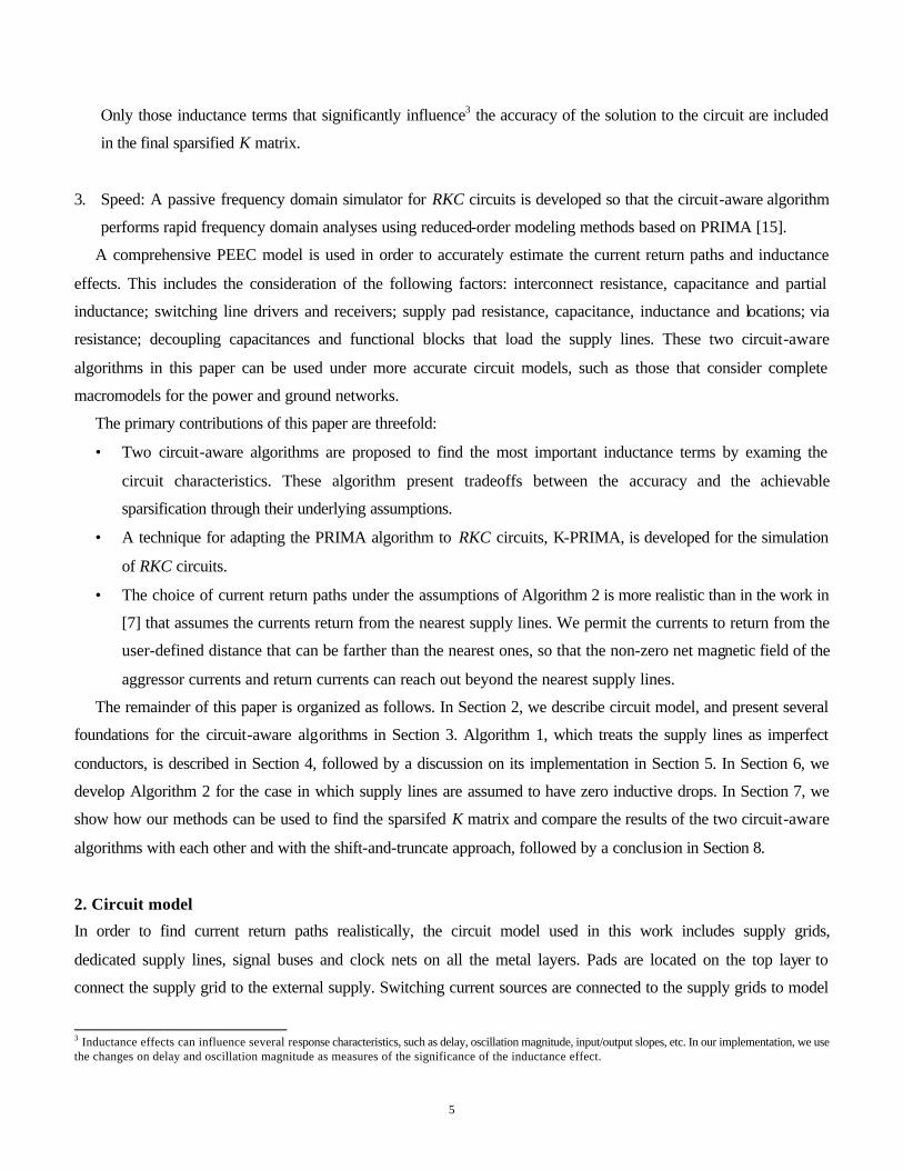
receiver. A typical cross sectional view of the layout is shown in Figure 1 and the specifics of the models are
detailed below and shown in Figure 2.
Figure 1: Cross-section of the topology. The lines marked P/G represent the power/ground (supply) lines, while the
region marked S represents a group of switching lines.
Figure 2: Schematic of a circuit with the ground grid and a switching line in PEEC model [8].
Line models: Each line is divided into line segments using an RLC4 model for each segment. The frequency-
independent resistance of any line segment is calculated as R= Rs L/W; Rs, L and W are, respectively, the sheet
resistance, length and width. The inductance of any line segment is calculated by Geometrical Mean Distance
(GMD) formulae in [2]. The line model also includes mutual inductances between any two non-perpendicular line
segments, and coupling capacitances between any two adjacent line segments. The line-to-ground and line-to-line
capacitances are calculated by Chern's model [16].
4 We start by using RLC model for line segments, but the final results of circuit -aware algorithms are sparsified K matrices.
M5
M4
M3
P/G S P/G
P/G P/G
M5
M4
M3
P/G S P/G
P/G P/G
External supply
Vd
Rd
Cload
Line to line capacitances
R L
Pad

7
Driver and receiver models: The drivers are modeled by a voltage source, an effective driver resistance and an
output capacitance. The receivers are modeled as a load capacitance connected to the ground grid. The effective
resistance of the driver is inversely proportional to the size, and the output capacitance of the driver and the load
capacitance are each proportional to the size of the corresponding entity, with differing constants of proportionality.
Pad and via model: Pads are located on the top metal layer and are modeled by a resistance, self-inductance and
pad-to-ground capacitance. Vias are modeled by resistances that connect supply lines on different layers.
Functional block model: Switching current sources are connected to the nodes of supply grids to model the
current drawn by the functional blocks connected to that node. The switching currents in a region are expressed as
∑ −i
tai iek , where each ta
i iek − is the current drawn by ith functional block in the region, and k i and ai represent the
magnitude and damping speed of the current, ranging from 10mA to 100mA and from 100ps to 400ps, respectively.
Non-switching gate model: A non-switching gate connected between supply grid is modeled as a resistance
sequentially connected with a decoupling capacitance.
All of the experiments carried out in this paper are on a 0.1µm technology, and the corresponding parameters
are extrapolated from [17]. These parameters are summarized as follows:
Minimum line width= 0.1 µm Driver resistance for minimum buffer size=23.9 KΩ
Minimum line spacing=0.14 µm Driver input capacitance for minimum buffer size=0.07 fF
The circuit topologies correspond to the top three metal layers, M5, M4 and M3, of a five layer metal structure,
with wide and long switching lines being routed on the uppermost metal layer.
Supply lines in the vertical direction are routed in M5 and M3, while those in the orthogonal direction are on
M4. Supply lines are further classified into two categories: grid supply lines and dedicated supply lines. Grid supply
lines form the main backbone of the power grid, and consist of a set of lines that are connected together through
vias, with direct connections to the external supply by pads. On the other hand, dedicated supply lines are
deliberately placed close to switching lines in order to provide good return paths for inductive currents. These lines
are connected to the power supply grid through vias. The vias resistance is taken to be 0.5Ω. Typical widths and
spacings of grid supply lines are 6.0µm and 54.0µm, respectively, while those of switching lines and the dedicated
supply lines are both 0.9µm. The thickness of metal layers and oxide layers are 0.5µm and 0.6µm, respectively.
Pads are located on M5 with spacing of 180µm. The resistance, capacitance and inductance of the pad are 0.0003Ω,
390fF and 0.15nH, respectively. The switching lines are driven by different sizes of drivers and the switching
waveforms for these drivers are chosen to excite the worst-case, where all lines are made to switch simultaneously
in such a way that the currents are carried in the same direction to enable the largest (and possibly pessimistic)
∑j
jij dtdIL )/( drop on the lines.

8
3. Proposed sparsification method
The motivation for the circuit-aware algorithm can be illustrated by considering the circuit equation:
∑+=j
jijiii dtdILIZV )/(
where Vi and Ii are the voltage across and the current flowing through line segment i, respectively; Zi is the
impedance of line segment i, not counting the inductance; Lij is the self-inductance (if i = j) or mutual inductance (if
i ≠ j) between segment i and j; dtdI j / is the rate at which the current in segment j changes with time. The
significance of the inductance effect of an aggressor line segment j on a victim line segment i depends on Lij (dIj /dt)
of the aggressor line segment and Zi Ii of the victim line segment, or in other words, on the relative magnitudes of
the terms in the above equation. Qualitatively speaking, strong inductance effects originate from the line segments
that have “large” dtdI j / and take effect on line segments that are “not far away” and with a “large” value of Lij as
well as a “small” value of Zi Ii. As an illustration of this, it can be seen that until recently, when on-chip inductances
were insignificant, RC modeling was adequate for all on-chip lines since the RC elements overwhelmed any
inductive coupling. The circuit-aware algorithm starts by finding ID lines that have a large value of dtdI j /
through ID line criterion and then groups nearby lines that have large values of Lij and small value of Zi Ii into a
cluster, so that a specified accuracy criterion is satisfied. The ID line criterion, the concept of a cluster, and the
detailed circuit-aware algorithm will be explained in the next several sections.
3.1 ID line criterion
A very simple but important observation for developing circuit-aware algorithms is that inductance-dominant lines
typically have a small transition time and a large oscillation magnitude and/or high frequency oscillation, so that
they are the best candidate lines (due to their large value of dtdI j / ) to cause mutual inductance effects on other
lines. To demarcate ID lines from RD lines, we use a relative criterion to define ID lines, called the ID criterion,
described as follows. This criterion is applied individually to one line at a time to determine whether it can be
classified as ID or not; recall that the line is divided into segments.
ID Criterion: A line is ID if the behavior of the output waveform in the presence of inductances (partial self-
inductances and mutual inductances only between any two segments on that line) is significantly different,
according to a specified metric, from the waveform when a pure RC model is used and inductances associated with
the line are ignored.
One such metric, used in our work, states that if the percentage variation in the oscillation magnitude is larger
than a specified ε , or the delay of the output response is larger than a specified δ, then the line is ID. RD lines
include all those lines that are not inductance-dominant. In this way, we separate all the on-chip lines into three
categories: ID switching lines, RD switching lines and supply lines.
9
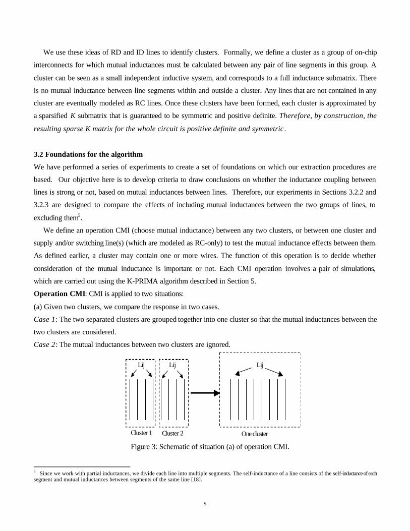
We use these ideas of RD and ID lines to identify clusters. Formally, we define a cluster as a group of on-chip
interconnects for which mutual inductances must be calculated between any pair of line segments in this group. A
cluster can be seen as a small independent inductive system, and corresponds to a full inductance submatrix. There
is no mutual inductance between line segments within and outside a cluster. Any lines that are not contained in any
cluster are eventually modeled as RC lines. Once these clusters have been formed, each cluster is approximated by
a sparsified K submatrix that is guaranteed to be symmetric and positive definite. Therefore, by construction, the
resulting sparse K matrix for the whole circuit is positive definite and symmetric .
3.2 Foundations for the algorithm
We have performed a series of experiments to create a set of foundations on which our extraction procedures are
based. Our objective here is to develop criteria to draw conclusions on whether the inductance coupling between
lines is strong or not, based on mutual inductances between lines. Therefore, our experiments in Sections 3.2.2 and
3.2.3 are designed to compare the effects of including mutual inductances between the two groups of lines, to
excluding them5.
We define an operation CMI (choose mutual inductance) between any two clusters, or between one cluster and
supply and/or switching line(s) (which are modeled as RC-only) to test the mutual inductance effects between them.
As defined earlier, a cluster may contain one or more wires. The function of this operation is to decide whether
consideration of the mutual inductance is important or not. Each CMI operation involves a pair of simulations,
which are carried out using the K-PRIMA algorithm described in Section 5.
Operation CMI: CMI is applied to two situations:
(a) Given two clusters, we compare the response in two cases.
Case 1: The two separated clusters are grouped together into one cluster so that the mutual inductances between the
two clusters are considered.
Case 2: The mutual inductances between two clusters are ignored.
Figure 3: Schematic of situation (a) of operation CMI.
5 Since we work with partial inductances, we divide each line into multiple segments. The self-inductance of a line consists of the self-inductance of each segment and mutual inductances between segments of the same line [18].
Lij
One cluster
Lij Lij
Cluster 1 Cluster 2

10
(b) Given one cluster and supply/switching line(s) modeled as RC-only6, we compare the response in two cases.
Case 1: The line(s) is (are) added into the cluster so that the mutual inductance between the cluster and the line(s)
as well the mutual inductances between segments on the line(s) are considered.
Case 2: The mutual inductances between the cluster and the line(s), as well as the mutual inductances between
segments on the line(s), are ignored.
In each situation above, the operation proceeds by carrying out simulations for both cases and testing the delays
and oscillation magnitudes of the outputs of switching lines in the two clusters or in the cluster and the switching
line(s) added into the cluster. If the change in one of the oscillation magnitudes [delays] is larger than an ε [δ], we
conclude that the mutual inductance between the clusters (or between the cluster and the supply and/or switching
line(s)) is important, implying that the two clusters should be grouped into one cluster, or the supply and/or
switching line(s) should be included into the cluster. A schematic CMI operation for situation (a) is shown in Figure
3. For two smaller clusters 1 and 2, if the mutual inductance effects between these two clusters are significant, the
two small clusters should be grouped into one large cluster that includes the mutual inductance terms between
cluster 1 and 2.
CMI in situation (b) can be used to test the relation between the cluster and the supply and/or switching line(s).
For example, if the RC-only line is a supply line, CMI is used to test whether the supply line is a good return path
of the cluster or not. If the RC-only line is a RD line, CMI determines whether the line is strongly influenced by the
cluster. In situation (b), the ID criterion has eliminated the possibility that mutual inductances along the RD line
could, on its own, cause significant inductive effects7. However, if the addition of mutual inductances with clusters
may result in significant effects on the cluster and/or the RD line, we should add the RD line into the cluster. In
Sections 3.2.1 and 3.2.2, we perform a set of experiments to derive a set of foundations that guide our approach.
6 Note that this differs from situation (a) above where, by definition, the lines consider mutual inductances within each cluster. 7 However, if this line is merged into the cluster as a result of the CMI operation, all mutual inductances within the cluster, including those between segments on the same line, can be considered.
11
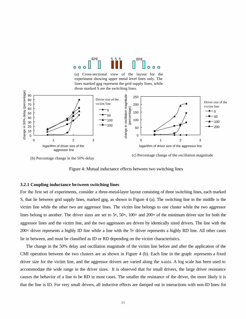
Figure 4: Mutual inductance effects between two switching lines
3.2.1 Coupling inductance be tween switching lines
For the first set of experiments, consider a three-metal-layer layout consisting of three switching lines, each marked
S, that lie between grid supply lines, marked gpg, as shown in Figure 4 (a). The switching line in the middle is the
victim line while the other two are aggressor lines. The victim line belongs to one cluster while the two aggressor
lines belong to another. The driver sizes are set to 5×, 50×, 100× and 200× of the minimum driver size for both the
aggressor lines and the victim line, and the two aggressors are driven by identically sized drivers. The line with the
200× driver represents a highly ID line while a line with the 5× driver represents a highly RD line. All other cases
lie in between, and must be classified as ID or RD depending on the victim characteristics.
The change in the 50% delay and oscillation magnitude of the victim line before and after the application of the
CMI operation between the two clusters are as shown in Figure 4 (b). Each line in the graph represents a fixed
driver size for the victim line, and the aggressor drivers are varied along the x-axis. A log scale has been used to
accommodate the wide range in the driver sizes. It is observed that for small drivers, the large driver resistance
causes the behavior of a line to be RD in most cases. The smaller the resistance of the driver, the more likely it is
that the line is ID. For very small drivers, all inductive effects are damped out in interactions with non-ID lines: for
0102030405060708090
0 1 2 3
logarithm of driver size of the aggressor line
chan
ge in
50%
del
ay (
perc
enta
ge)
5
50100
200
Driver size of the victim line
(b) Percentage change in the 50% delay
0
50
100
150
200
250
0 1 2 3
logarithm of driver size of the aggressor line
chan
ge in
osc
illat
ion
mag
nitu
de
(per
cent
age)
5
50
100
200
Driver size of the victim line
(c) Percentage change of the oscillation magnitude
gpg s s s gpg
gpg gpg S S S
(a) Cross-sectional view of the layout for the experiment showing upper metal level lines only. The lines marked gpg represent the grid supply lines, while those marked S are the switching lines.

12
example in Figure 4, for a victim line with a 5× driver size, the delay as well as the oscillation magnitude are not
easily influenced by the mutual inductance of non-ID aggressor lines. When the aggressor lines are highly ID, the
delay of the victim line with the 5× driver changes significantly, though its oscillation magnitude remains zero.
Victim lines that are moderately or highly ID are significantly affected by aggressor lines, even when the
aggressor lines are not highly ID. Highly RD lines have small effects on victim lines. It can be seen that when a 5×
driver is used in the victim line, the delay and oscillation magnitude changes in the victim are negligible except
when the driver size of the victim lines are larger than 100×. However, if the driver size of the aggressor line is
changed from 5× to 50× or larger, it is seen that the mutual inductances can perceptibly affect the waveform of any
victim line that is not highly RD, both in terms of the delay and the oscillation magnitude.
Figure 5: Significant interactions between aggressors and victims.
From the above simulation results, we can infer the first set of foundations:
Foundation 1: ID lines have strong mutual inductance effects on other ID lines. ID victim lines are easily
influenced by aggressor lines. The more ID a switching line is, the more significant the effect is.
Foundation 2: RD lines, especially highly RD lines, have very little mutual inductance effects on other lines.
Moreover, highly RD lines are not easily influenced by aggressor lines unless they are highly ID.
Foundation 3: Moderately ID lines may have mutual inductance effects on moderately RD lines.
These foundations can be summarized in the interaction graph in Figure 5. The vertices in this graph correspond to
aggressor lines to the left and victim lines to the right, considering the possibilities of them being potentially ID,
RD or intermediate. The edges between the vertices show the cases in which the interactions can be ignored.
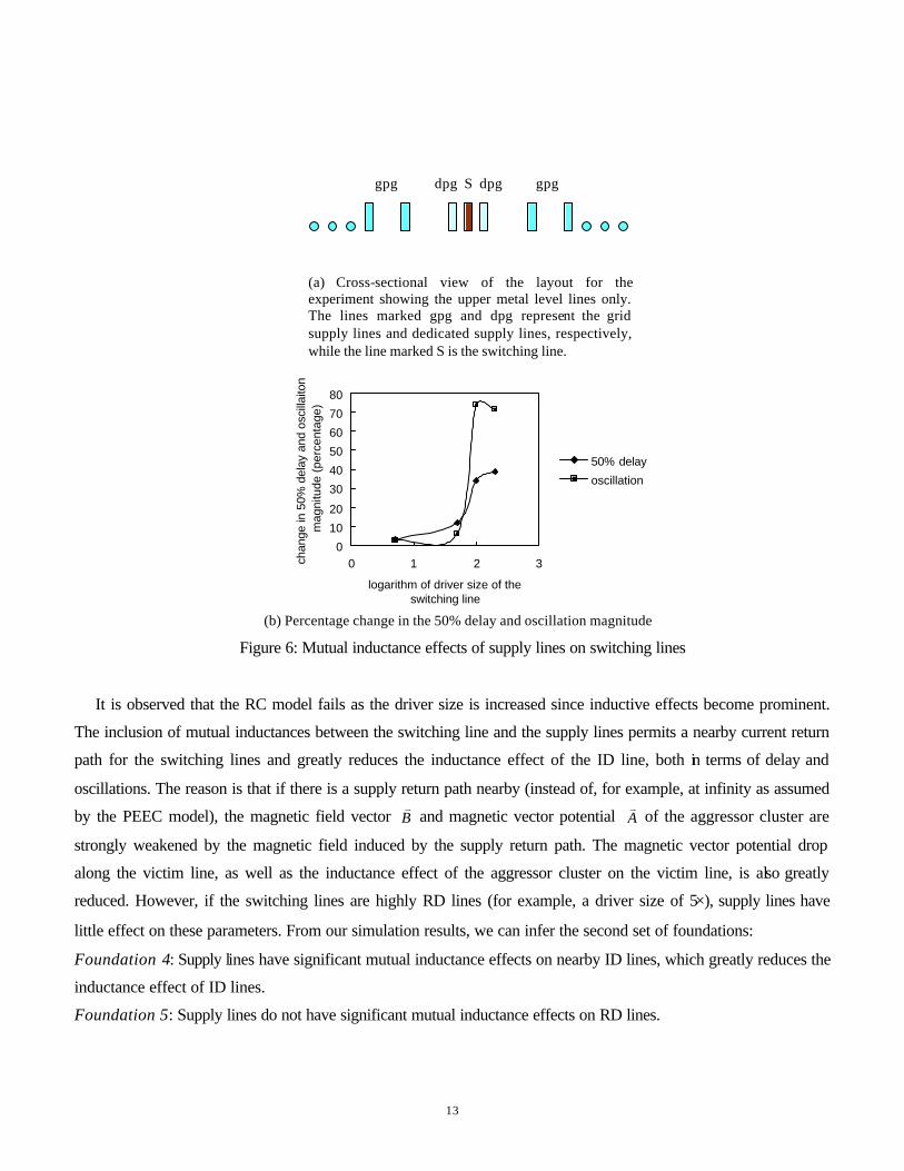
3.2.2. Coupling between switching lines and supply lines
In the next set of experiments, the experimental setup is similar to Section 3.2.1, except that there is only one
switching line that lies between two dedicated supply lines, as shown in Figure 6 (a). Initially the switching line
forms one cluster and the two dedicated supply lines are modeled as RC-only. The driver sizes of the switching line
are set to 5×, 50×, 100× and 200× of the minimum driver size. After the application of CMI operations on the
cluster and the two dedicated supply lines, the changes in the 50% delay and oscillation magnitude of the switching
line are shown in Figure 6 (b).
Highly ID Moderately ID Moderately RD Highly RD AGGRESSOR
Highly ID Moderately ID Moderately RD Highly RD VICTIM
13
Figure 6: Mutual inductance effects of supply lines on switching lines
It is observed that the RC model fails as the driver size is increased since inductive effects become prominent.
The inclusion of mutual inductances between the switching line and the supply lines permits a nearby current return
path for the switching lines and greatly reduces the inductance effect of the ID line, both in terms of delay and
oscillations. The reason is that if there is a supply return path nearby (instead of, for example, at infinity as assumed
by the PEEC model), the magnetic field vector Bv
and magnetic vector potential Av
of the aggressor cluster are
strongly weakened by the magnetic field induced by the supply return path. The magnetic vector potential drop
along the victim line, as well as the inductance effect of the aggressor cluster on the victim line, is also greatly
reduced. However, if the switching lines are highly RD lines (for example, a driver size of 5×), supply lines have
little effect on these parameters. From our simulation results, we can infer the second set of foundations:
Foundation 4: Supply lines have significant mutual inductance effects on nearby ID lines, which greatly reduces the
inductance effect of ID lines.
Foundation 5: Supply lines do not have significant mutual inductance effects on RD lines.
(a) Cross-sectional view of the layout for the experiment showing the upper metal level lines only. The lines marked gpg and dpg represent the grid supply lines and dedicated supply lines, respectively, while the line marked S is the switching line.
gpg dpg dpg gpg
gpg dpg S dpg gpg
0
10
20
30
40
50
60
70
80
0 1 2 3
logarithm of driver size of the switching line
chan
ge in
50%
del
ay a
nd o
scill
aito
n m
agni
tude
(pe
rcen
tage
)
50% delay
oscillation
(b) Percentage change in the 50% delay and oscillation magnitude

14
3.3 Formation of clusters
Based on the above foundations, we separate the six possible combinations of mutual inductance interactions
between ID lines, RD lines and supply lines into two classes:
1. Strong mutual inductance interactions between
♦ ID lines and nearby ID lines
♦ ID lines and nearby supply lines
2. Weak mutual inductance interactions between
♦ ID lines and nearby RD lines
♦ Moderately RD lines and nearby supply lines
♦ Moderately RD lines and nearby moderately RD lines
♦ Supply lines and nearby supply lines
Since strong mutual inductance interactions are the most important, our algorithm first identifies strong mutual
inductance terms and forms clusters, and then adds weak mutual inductance terms into those clusters if necessary.
In order to reduce as many of the mutual inductance terms as possible, our algorithms always find the supply return
paths for a cluster before we determine which other clusters or RD lines it will affect. On the other hand, if we
consider the mutual inductance effect between the aggressor cluster and victim cluster/line without incorporating
the effect of the supply return path, it is very possible that we may overestimate the inductance effect of the
aggressor cluster and include more interactions than is necessary (and consequently reducing the sparsification).
BASIC STEPS: We proceed by selectively including a new set of inductive effects in each iterative step. There are
four basic steps in the two algorithms in this paper, and each of these steps is typically applied repeatedly, a number
of times:
1. Use the ID criterion to check whether a switching line is an ID line or not and form a preliminary set of
clusters, each of which consists of a single ID line.
2. Check whether a single supply line is one of the return paths for a cluster by applying CMI on the cluster
and the supply line. If CMI shows a large mutual inductance effect, the supply line is an important current
return path and should be included into the cluster. If the cluster only includes one ID line, only strong
interactions are considered in this step; otherwise, both strong and weak interactions are considered.
3. Check whether a single RD line is greatly influenced by a cluster by applying CMI on the cluster and the
RD line. If there is a large mutual inductance effect, the RD line should be included into the cluster. Only
weak interactions are considered in this step.
4. Check if two clusters created so far have important mutual inductance effects between each other by
applying CMI on these two clusters. If all lines in the two clusters are ID lines and their associated supply
15
return paths, the interactions considered here are strong interactions; otherwise, both strong and the weak
interactions are taken into account in this step.
The above basic steps consider the circuit structure and interconnections between circuit elements and form the
basis for the circuit-aware algorithms. A critical issue is to determine which supply lines, RD lines and other
clusters on chip should be tested for the CMI operation with a given cluster. The following section describes a
method to choose candidate lines and clusters, which greatly reduced the number of tests needed to be performed.
The lines and clusters found by the method have a large possibility of having a significant mutual inductance
interaction with the cluster in consideration.
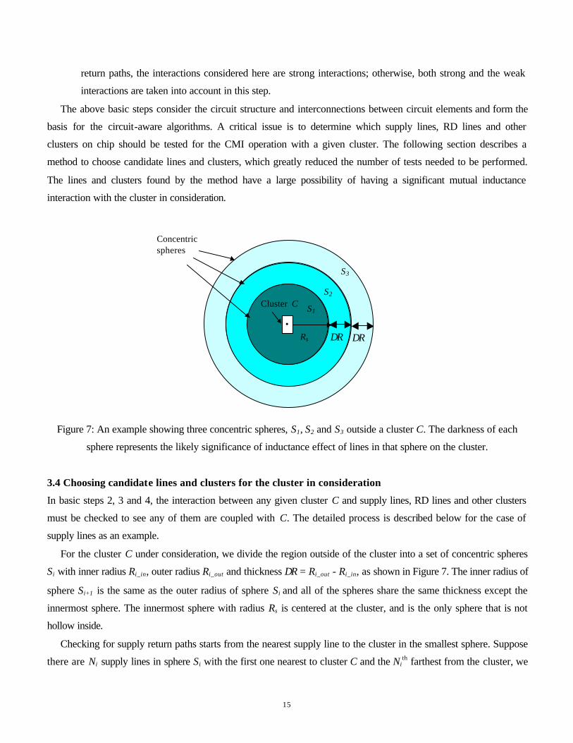
Figure 7: An example showing three concentric spheres, S1, S2 and S3 outside a cluster C. The darkness of each
sphere represents the likely significance of inductance effect of lines in that sphere on the cluster.
3.4 Choosing candidate lines and clusters for the cluster in consideration
In basic steps 2, 3 and 4, the interaction between any given cluster C and supply lines, RD lines and other clusters
must be checked to see any of them are coupled with C. The detailed process is described below for the case of
supply lines as an example.
For the cluster C under consideration, we divide the region outside of the cluster into a set of concentric spheres
Si with inner radius Ri_in, outer radius Ri_out and thickness ∆R = Ri_out - Ri_in, as shown in Figure 7. The inner radius of
sphere Si+1 is the same as the outer radius of sphere Si and all of the spheres share the same thickness except the
innermost sphere. The innermost sphere with radius Rs is centered at the cluster, and is the only sphere that is not
hollow inside.
Checking for supply return paths starts from the nearest supply line to the cluster in the smallest sphere. Suppose
there are Ni supply lines in sphere Si with the first one nearest to cluster C and the Nith farthest from the cluster, we
Rs ∆R ∆R •
Cluster C
Concentric spheres
S1
S2
S3

16
start the checking with the first supply line by applying CMI on cluster C and the supply line. If the supply line has
a strong effect on the cluster, then it is added into the cluster temporarily8 and CMI is then applied on the enlarged
cluster and the next nearest supply line; otherwise, CMI is applied between cluster C and the next nearest supply
lines. If we do not make this temporary addition to the cluster, it is possible that we will overestimate the number of
supply lines needed by the cluster. If there is at least one supply line in sphere Si that has a strong influence on the
cluster C at the center, we test the next sphere Si+1. If there is no supply line in Si that is important, we conclude that
no other supply lines in spheres larger than Si are important and the check for supply return paths for cluster C is
concluded.
This procedure uses an inherent assumption that the nearer the supply line is to the cluster, the larger its effect on
the cluster is likely to be. The rationale for using this assumption is that nearer supply lines have larger values of
mutual inductance with cluster C, so that they are most likely to influence the inductive behavior of the cluster. This
is also empirically observed. This assumption may not always be correct since it is very possible that a supply line
that is a little nearer to the cluster does not have a large effect, perhaps because of its large line resistance, while a
supply line that is a little farther away has large effect on the cluster. To overcome this problem in a simple way, the
above process with the concept of spheres with thickness ∆R is utilized. Therefore, even if in the extreme case,
where only the farthest supply line in sphere Si has a strong effect on cluster C while the other supply lines in that
sphere have no large effect on C, the supply lines in sphere Si+1 just outside Si will still be checked according to the
process described above.
The effectiveness of this process depends on the value of Rs and ∆R. If Rs and ∆R are rather large, then all of the
supply lines on the chip may be checked, so that this process brings us no error in the way of choosing supply lines.
However, this is computationally expensive. On the other hand, if there is only one line in each sphere, then
perhaps only one supply line may be checked, which is clearly an incorrect analysis for a design with poorly placed
return paths. However, for a good design where supply lines are effective and the magnetic field is localized tightly
at nearby region of a cluster, even one supply line per sphere may work well. The values of Rs and ∆R are user-
specified.
The above process is used not only in the step of finding supply return paths, but also used in the steps that find
RD lines and other clusters that cluster C influence. The only differences in the process for the latter two steps are
that the candidates for addition to C are not supply lines, but RD lines and/or clusters, and if these have a strong
interaction with cluster C, they are not temporarily grouped into C. The addition of RD lines and/or other clusters
into cluster C will strengthen the cumulative magnetic field of cluster C, which in turn may need more supply
return paths to be added to C to weaken this magnetic field; if we were to add RD lines and/or other clusters into
cluster C without looking for more supply return paths before checking for inductance effect between this enlarged
8 The reason why these additions are considered “temporary” is that whenever a new cluster is considered, even supply lines that were previously incorporated into another cluster are taken to be candidate return paths. As a result of this, the clusters that are formed do not depend on the sequence in which the original
17
cluster and other RD lines and/or clusters, it is possible that we would overestimate the inductance effect of cluster
C.
In the succeeding sections, we present two algorithms for creating clusters that use the above framework.
4. Circuit-aware Algorithm 1
4.1 Description of Algorithm 1
From the previous discussion, it is clear that the main idea in the circuit-aware algorithm is to find the most
important inductance terms first, followed by heuristically adding weak inductance terms into clusters, so that the
clusters increase in size until they do not grow any more. The algorithm always tries to drop off as many
unimportant inductance terms as possible.
The oscillation on the supply lines because of the high pad impedance, the switching current drawn by the
functional blocks connected to supply lines and the mutual inductance effects of nearby switching lines all serve to
reduce the integrity of supply lines, which can potentially impact the output response significantly. Therefore, if our
objective is to obtain high accuracy modeling, we should realistically consider the RKC’s associated with the
supply lines. Algorithm 1 is a circuit-aware algorithm that operates under such a model for supply lines, where the
magnetic field of switching lines is considered to be capable of reaching infinity (or more realistically, the chip-
size) and influencing the response of other switching lines and the integrity of faraway supply lines.
Algorithm 1 is a combination of the basic steps described in Section 3.3, as depicted in the flow chart in Figure
8. It is an iterative method in which the output response is brought closer to the accurate response in each iteration.
The algorithm begins by using a RC model for all lines. After applying the ID criterion, each ID line forms a
cluster, called an ID cluster, with only one line in it. It is worth pointing out that throughout the algorithm, each
cluster includes at least one ID line.
Once this is done, we would like to attempt to combine clusters taking into account strong interactions between
pairs, a pair of clusters at a time. However, as stated earlier, return paths through nearby supply lines may greatly
reduce the inductive effects of a cluster as calculated from the partial inductances, and consequently, the strong
interactions of the cluster with other clusters. Therefore, it is important to first consider interactions between a
cluster with nearby supply lines9. We will refer to the set of clusters at the beginning of this step as the “original
clusters.”
The method for finding the supply return paths10 is outlined as step 2 in Section 3.3 and in Section 3.4. The
choice of the supply line to be included in the original cluster is heuristically made by selecting the nearest supply
lines one at a time and applying step 2, possibly enlarging the cluster after each such line is considered.
clusters were processed and some supply lines may be temporarily assigned to more than one cluster. 9 If supply line interactions are not considered before other interactions, the algorithm will not result in incorrect results, but it may be unduly pessimistic and may create larger clusters than is necessary, leading to less sparse K matrices. 10 Note that this does not imply that these are the only return paths; other return paths are identified later.
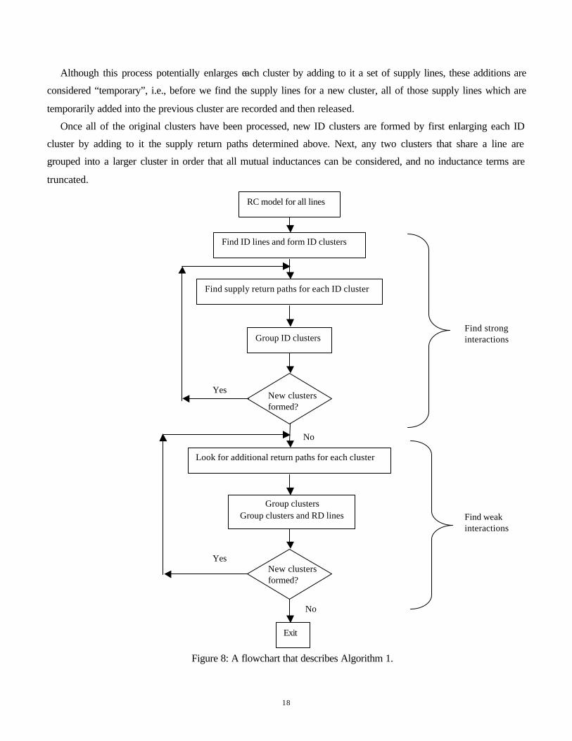
18
Although this process potentially enlarges each cluster by adding to it a set of supply lines, these additions are
considered “temporary”, i.e., before we find the supply lines for a new cluster, all of those supply lines which are
temporarily added into the previous cluster are recorded and then released.
Once all of the original clusters have been processed, new ID clusters are formed by first enlarging each ID
cluster by adding to it the supply return paths determined above. Next, any two clusters that share a line are
grouped into a larger cluster in order that all mutual inductances can be considered, and no inductance terms are
truncated.
Figure 8: A flowchart that describes Algorithm 1.
RC model for all lines
Find ID lines and form ID clusters
Find supply return paths for each ID cluster
Group ID clusters
New clusters formed?
Look for additional return paths for each cluster
Group clusters Group clusters and RD lines
No
Yes
New clusters formed?
Exit
Yes
No
Find strong interactions
Find weak interactions

19
The next step after finding supply return paths is to check if two ID clusters have a strong mutual inductance
interaction between them. The process of checking strong interaction between ID clusters is described in step 4 in
Section 3.3 and Section 3.4. The clusters that have strong interactions are grouped into larger clusters. Again, to
avoid the pitfalls associated with truncating inductance values, two clusters that have a strong interaction with at
least one common cluster are combined into the same cluster, even if they do not mutually have a strong
interaction. The above process of finding supply return paths and finding strong interactions are repeated until no
new mutual inductance interactions are found and no new clusters are formed. At the end of this process, all of the
strong mutual inductance interactions have been identified.
Next, we check for weak mutual inductance effects that correspond to the interaction between two nearby
clusters or between one cluster and one nearby RD line. Before checking for this, additional return paths should be
identified for each cluster using a technique that is similar to that used for the original clusters. To identify these
weak mutual inductance interactions, we apply the method described in steps 3 and 4 in Section 3.3 along with the
technique in Section 3.4. The above process of finding additional supply return paths and finding weak interactions
among clusters and RD lines is repeated until no new mutual inductance interactions are found and no new clusters
are formed.
In this way, all the important inductance terms are included in final clusters with a high sparsification.
4.2 Computational cost of the circuit-aware algorithms
To evaluate the computational cost of our algorithms, consider a circuit with N lines, which have at most nseg
segments on each line. It can be seen in Figure 8 that there are three main parts in the circuit-aware algorithm:
finding ID lines, finding strong interactions and finding weak interactions. Since the first part processes each line
individually, its cost is linear in the number of lines, and hence, the latter two parts are dominant in the total
computational cost. We estimate their complexity under reasonable assumptions as follows.
In the worst case, all lines are initially identified as ID, and all of these lines eventually are added into the same
cluster, with one line being added into the cluster in each iteration. Without loss of generality, let us assume that
after the first iteration, the first and the second ID lines are grouped into an intermediate cluster with two lines in it,
while all the other ID lines are kept alone in their own cluster; after the third iteration, the third ID line is added
into the intermediate cluster, which now has three lines in it, while the other ID lines are alone as before, and so on.
Therefore, after N-1 iterations all lines are grouped into one final cluster, and the upper bound of the total number
of iterations is O(N). Suppose nCMI is the upper bound on the number of CMI operations for each cluster;
practically, this is seen to be bounded by a constant.
The computational cost of one CMI operation, which includes two simulations, between two original clusters is
O(nseg), so that the cost in the first iteration is O(nCMI×N×nseg). In the second iteration, there are N-1 clusters, of

20
which one cluster is the enlarged intermediate cluster with at most 2×nseg segments in it, while the other clusters are
still the lone ID lines, each with at most nseg segments. One of these ID lines is now added to the cluster in the
second iteration, with a computational cost of O(nCMI× (N-2) ×nseg+ nCMI×2×nseg) = O(nCMI×N×nseg), which is the
same as the computational cost for the first step. The same conclusion can be derived for the third iteration, the
forth iteration, and so on. Therefore, the total complexity for N iterations is O(nCMI×N2×nseg).
In practice, the number of iterations is much smaller than N. There are two reasons for this. Firstly, it is usually
the case that there will be a small number of lines in a cluster, and it is highly unlikely that all lines will be grouped
into a single final cluster. In a typical layout, for example, with a clock net or signal buses and a dense power grid
distribution on the upper several metal layers, the influence of the magnetic field of ID lines is very localized, so
that faraway lines do not have to be added to the clusters of the ID lines. Secondly, after each iteration, more than
one line could be added into a cluster as clusters containing several linesare combined to create still larger clusters,
so that cluster growth can be rela tively rapid. Due to these effects, it was empirically observed that the total
number of iterations can be bounded by a constant, and as a result, the complexity is typically O(N×nCMI).
5. Implementation of K-PRIMA
As stated in Section 1, we use the K element [13] to represent the inductance system in our algorithm. This is based
on the idea of representing inductive effects using the inverse of the inductance matrix. We adapt the PRIMA
algorithm [15] in order to generate a simulator, K-PRIMA, which can work with K elements and guarantee the
passivity of the reduced system. This simulator is used numerous times in our algorithm, twice in each CMI
operation. Starting with the traditional inductance matrix M, simulation in each step of algorithm requires solving
the following system of differential equations, which are formed using the Modified Nodal Analysis (MNA)
approach:
BxsCG =+ )( (4)
−
=0TE
ENG
=
M
QC
0
0
=
i
vx (5)
where (G+sC) is the admittance matrix, x is a vector of unknown node voltages and unknown currents of inductors
and voltage sources, B is a vector of independent time-varying voltage and current sources, and M is the
traditionally used inductance matrix. In order to guarantee passivity, a sufficient condition [15] is to ensure that the
off-diagonal submatrices have a negative transpose relation in the G matrix and that N, Q, and M be symmetric and
positive definite. In order to introduce K matrix into (4) and at the same time satisfy the above requirement, the
second set of equations implied by (4) are adapted as follows:
0=+− sMivET (6)
Since M is symmetric and positive definite, it can be Cholesky-factored as M = L LT. Substituting this Cholesky
factorization in (6) above, we obtain

21
0=+− isLLvE TT (7)
Premultiplying (7) by L-1, we get
01 =+− − isLvEL TT (8)
Now we define bT iiL = and rewrite (8) as
01 =+− −b
T sivEL (9)
The first set of equations in (4) can then be rewritten as
bsQviLENv bT =++ −1)( (10)
Therefore, from (9) and (10) the MNA matrix can be written as:
−=
−
−
0
)(1
1
T
T
EL
LENG
=I
QC
00
=
biv
x (11)
It can be verified that the construction of (11) satisfies the requirements of preservation of passivity of PRIMA as
described in [15], since the proof of passivity in [15] requires the off-diagonal blocks in G to be negative transposes
of each other.
Since 1111 )()( −−−− === LLLLMK TT , L-1 is also a factor of K matrix and both K and L-1 have the
property of locality. Our approach to find the sparsified L-1 is adapted from the method to find Kall matrix described
in [13]. A further simplification is possible: the K submatrix for each cluster is built independently of the other
clusters since there are no mutual inductance terms between clusters. Therefore, in constructing the window for
finding the submatrix of K for a given cluster, it is necessary only to consider wires within the cluster. This allows
greater adaptability: the window sizes and shapes may be different for different clusters since the windowing
operations are applied to different clusters independently.
The following is our approach to construct the sparsified L-1 matrix (the notation used here is similar to [13]):
1. For each aggressor line segment i, find a traditional inductance matrix Msmall including the line segments
that lie within the cluster that i belongs to and lie within in a small window size around i.
2. Cholesky-factorize Msmall to find the Cholesky factor Lsmall, which is a lower triangular matrix.
3. Invert Lsmall.
4. Compose the large system L-1 by the column corresponding to the aggressor line segment in 1−smallL .
Using this approach, the K and L-1 matrices can be greatly sparsified and save a large amount of computational cost.
6. Circuit-Aware Algorithm 2
Algorithm 1 applies to the most realistic case with imperfect supply lines. However, for a very well designed
supply grid or in cases where the requirement to the accuracy of modeling is not very high, the ∑j
jij dtdIL )/(
drop on the supply grid can be assumed to be zero and the supply grid can be assumed to be perfect in this respect.
22
However, we point out that we do consider the RC drops in supply lines, and that we do not consider the supply
lines to be perfect ground planes. Algorithm 2 is another version of the circuit-aware algorithm with such an
assumption and is developed as an extension of Algorithm 1. Specifically, we assume that the currents return from
the supply lines within a user-defined distance. Within this distance, we assume that the ∑j
jij dtdIL )/( drops on
the supply lines are zero (but the RC drops could be nonzero), while outside this distance, the net magnetic field of
the aggressor lines and the return currents is zero. A similar assumption was also made in the work in [7] and apart
from the fact that [7] is not circuit-aware, a primary difference between our work and theirs is that we allow
currents to return from the supply lines beyond the nearest supply lines, so that the switching lines can have mutual
inductance coupling with other switching lines beyond the nearest supply lines, unlike [7], which assumes that the
currents return from the nearest supply lines and that the switching lines in different interaction regions defined by
“halo rules” are completely decoupled. In reality, only a perfect, infinitely large conductor plate can fully decouple
the magnetic field and an on-chip metal line only partially blocks the magnetic field. This weakened magnetic field
can influence the switching lines outside the nearest supply lines, and except in a very good design, such an
influence can reach far away.
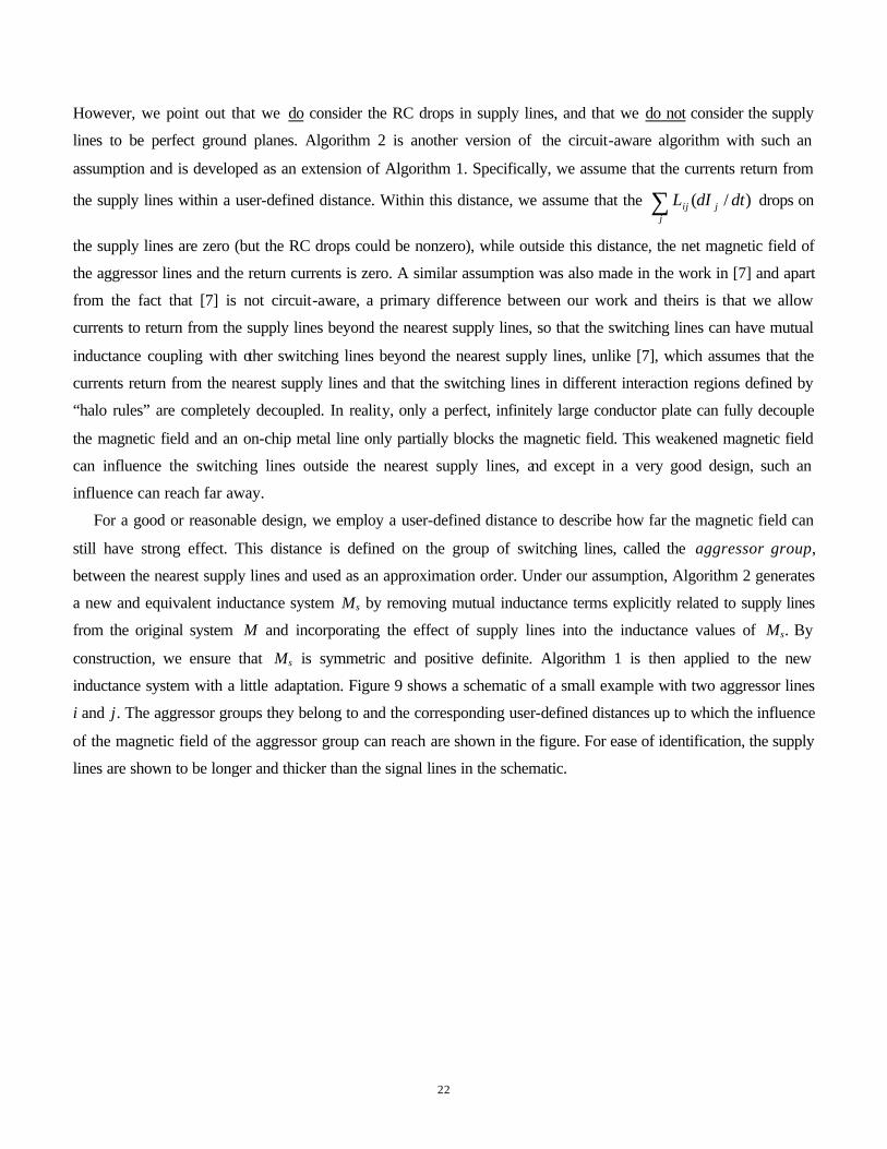
For a good or reasonable design, we employ a user-defined distance to describe how far the magnetic field can
still have strong effect. This distance is defined on the group of switching lines, called the aggressor group,
between the nearest supply lines and used as an approximation order. Under our assumption, Algorithm 2 generates
a new and equivalent inductance system Ms by removing mutual inductance terms explicitly related to supply lines
from the original system M and incorporating the effect of supply lines into the inductance values of Ms. By
construction, we ensure that Ms is symmetric and positive definite. Algorithm 1 is then applied to the new
inductance system with a little adaptation. Figure 9 shows a schematic of a small example with two aggressor lines
i and j. The aggressor groups they belong to and the corresponding user-defined distances up to which the influence
of the magnetic field of the aggressor group can reach are shown in the figure. For ease of identification, the supply
lines are shown to be longer and thicker than the signal lines in the schematic.
23
Figure 9: A schematic showing a set of aggressor lines, aggressor groups and the user-defined distances. The
dashed line shows the user-defined distance for aggressor group gi, while the dash-dot line is the user-defined
distance for aggressor group gj.
6.1. Definition and formation of the new matrix Ms
For a layout including both supply lines and switching lines, the device equation of inductors can be written as
=
s
pgT
s
pg
II
MMMM
sVV
2212
1211 (12)
where Vpg and Vs represent the voltages difference across line segments on supply lines and switching lines,
respectively, Is and Ipg are the currents in these line segments on the switching and supply lines, respectively, and
M11, M12 and M22 are inductance submatrices. For ease of exposition, we will work with the inductance matrices
here instead of the K matrices, although the implementation uses the K matrix representation.
Since the supply lines are assumed to have no ∑j
jij dtdIL )/( drop, Vpg should be the zero vector. Therefore,
the first set of equations can be written as:
spg IMMI 121
11−−= (13)
Substituting (13) into the second set of equations yields
sssT
s IsMIMMMMsV =−= − )( 121
111222 (14)
Aggressor group gi
line i
User-defined distance of aggressor group gi
line j
Aggressor group gj
User-defined distance of aggressor group gj

24
The calculation of Ms can be very efficient since M is symmetric and positive definite and can be Cholesky factored
as:
TT
TT
T LLL
LLLL
L
MM
MMM =
=
=
22
2111
2221
11
2212
1211
0
0
A few algebraic manipulations lead to the result
121
111222 MMMMM Ts
−−=
TTTTT LLLLLLLLLL 21111
1111112122222121 )( −−+=
TLL 2222= (15)
Since L22 and L22T are triangular matrices, the computation for (14) is greatly reduced.
It is easy to prove that the new inductance matrix Ms is symmetric and positive definite. We can think of Ms as a
partial inductance matrix for a new inductance system, and as a substitute of the original system M, but with better
locality properties. This locality provides further sparsification above and beyond that obtained by dropping the
inductance terms explicitly related to the supply lines.
6.2 Locality of matrix Ms
We now present an example to demonstrate the locality of the Ms matrix. The layout includes six parallel lines as
shown in Figure 10. Both the width and the spacing of each line are 0.9µm and the height of each line is 0.5µm.
Each line is cut into ten line segments with 60µm per segment. The first and sixth lines, marked P/G, are supply
lines, while the other four lines, S1 through S4, are switching lines.
Figure 10: A layout example of six 600µm -long lines. The lines marked P/G represent the power/ground (supply)
lines, while those marked S1 through S4 are the switching lines.
The mutual inductance matrix M, a 60×60 matrix, is calculated using GMD formulæ for partial inductances.
Here we only show a part of M to demonstrate how the value of mutual inductance is changed under our
assumption of zero inductive drops on the supply lines. The columns of M correspond to the first three consecutive
line segments of S1, followed by the first line segment of S2, S3 and S4, respectively. The first line segment on
each line faces the first line segment on its nearest lines. The matrix Ms is obtained using the procedure described
above.
P/G S1 S2 S3 S4 P/G
Length=600µm
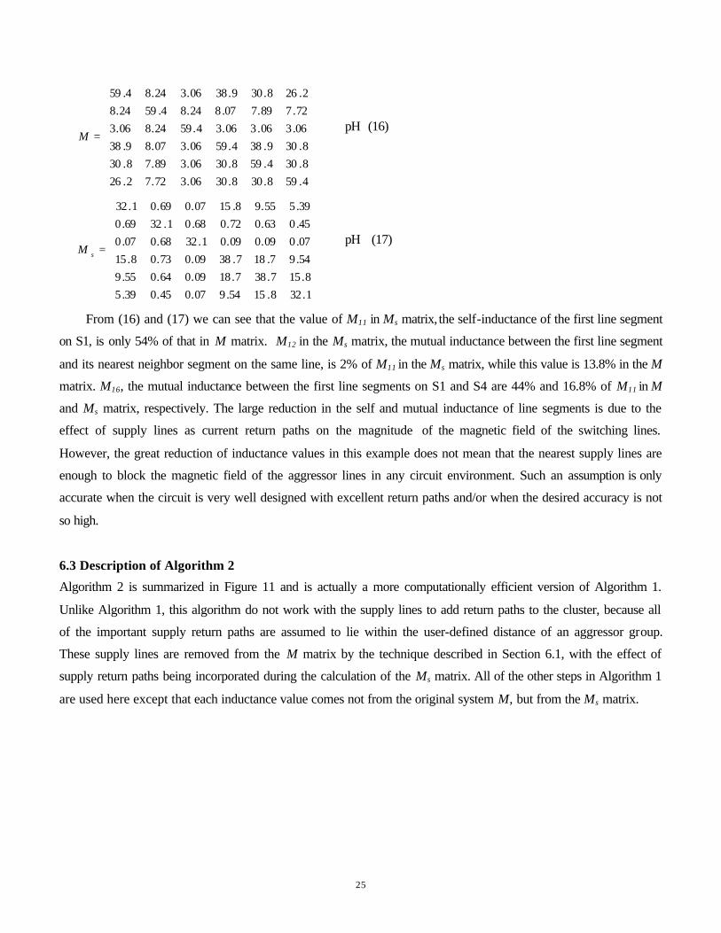
25
=
4.598.308.3006.372.72.268.304.598.3006.389.78.308.309.384.5906.307.89.38
06.306.306.34.5924.806.372.789.707.824.84.5924.8
2.268.309.3806.324.84.59
M pH (16)
=
1.328.1554.907.045.039.58.157.387.1809.064.055.9
54.97.187.3809.073.08.1507.009.009.01.3268.007.045.063.072.068.01.3269.039.555.98.1507.069.01.32
sM pH (17)
From (16) and (17) we can see that the value of M11 in Ms matrix, the self-inductance of the first line segment
on S1, is only 54% of that in M matrix. M12 in the Ms matrix, the mutual inductance between the first line segment
and its nearest neighbor segment on the same line, is 2% of M11 in the Ms matrix, while this value is 13.8% in the M
matrix. M16, the mutual inductance between the first line segments on S1 and S4 are 44% and 16.8% of M11 in M
and Ms matrix, respectively. The large reduction in the self and mutual inductance of line segments is due to the
effect of supply lines as current return paths on the magnitude of the magnetic field of the switching lines.
However, the great reduction of inductance values in this example does not mean that the nearest supply lines are
enough to block the magnetic field of the aggressor lines in any circuit environment. Such an assumption is only
accurate when the circuit is very well designed with excellent return paths and/or when the desired accuracy is not
so high.
6.3 Description of Algorithm 2
Algorithm 2 is summarized in Figure 11 and is actually a more computationally efficient version of Algorithm 1.
Unlike Algorithm 1, this algorithm do not work with the supply lines to add return paths to the cluster, because all
of the important supply return paths are assumed to lie within the user-defined distance of an aggressor group.
These supply lines are removed from the M matrix by the technique described in Section 6.1, with the effect of
supply return paths being incorporated during the calculation of the Ms matrix. All of the other steps in Algorithm 1
are used here except that each inductance value comes not from the original system M, but from the Ms matrix.

26
1. Use the new values of self and mutual inductance in Ms to find ID lines, and form ID clusters using the ID
criterion.
2. Check all ID clusters to see if any two of them should be grouped into one larger cluster. At the end of this
process, if any two of the newly formed clusters have common lines, group them into one cluster. Repeat step 2
until no new cluster is formed.
3. Test to see if any two clusters, or one cluster and one RD line, should be combined into one cluster. At the end
of this process, if any two of the newly formed clusters have common lines, group them into one cluster. Repeat
step 3 until no new cluster is formed.
Figure 11: Outline of Algorithm 2
7. Experimental results
We have carried out a set of experiments on a 0.1µm technology to examine the correctness of our assumptions and
the effectiveness of our algorithms. Specifically, we study the effect of dedicated supply lines on reducing
inductive effects, compare the results of Algorithm 1 and 2, compare Algorithm 1 with the shift-and-truncate
method and demonstrate the effect of altering the user-defined distance in Algorithm 2. We also analyze our results
to outline techniques for optimizing inductance effects. The circuit topologies used in this section are based on the
models and layer assignments described in Section 2, and in all cases, a voltage swing of 1V is used.
7.1 Comparison of the accuracy of Algorithms 1 and 2 with the exact response
Two sets of experiments are performed in this section on two different configurations to compare the effectiveness
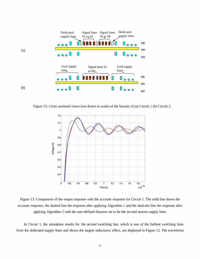
of Algorithms 1 and 2 with each other. The cross sections of the layouts of Circuit 1 and 2 are as shown in Figure
12. In Circuit 1, there are 10 vertical grid supply lines in M5, with 8 switching lines and 3 dedicated supply lines
between the 5th and 6th grid supply lines. There are 10 vertical grid supply lines on M3 and 21 horizontal grid
supply lines on M4. The driver sizes of the 8 switching lines named, from left to right, S1 through S8, are 100×,
200×, 10×, 100×, 100×, 5×, 50×, and 200×, respectively. The three dedicated supply lines are positioned,
respectively, to the left of the first switching line, between the fourth and fifth switching lines, and to the right of
the eighth switching line. Circuit 2 is identical to Circuit 1 in all respects, except that all dedicated supply lines are
removed, so that it is a “worse” design than Circuit 1.
27
(a)
(b)
Figure 12: Cross sectional views (not drawn to scale) of the layouts of (a) Circuit 1 (b) Circuit 2.
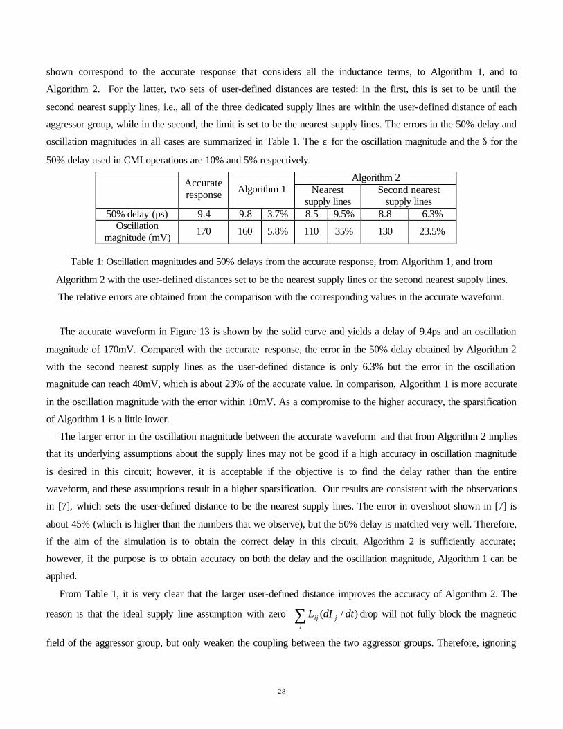
Figure 13: Comparison of the output response with the accurate response for Circuit 1. The solid line shows the
accurate response, the dashed line the response after applying Algorithm 1 and the dash-dot line the response after
applying Algorithm 2 with the user-defined distance set to be the second nearest supply lines.
In Circuit 1, the simulation results for the second switching line, which is one of the farthest switching lines
from the dedicated supply lines and shows the largest inductance effect, are displayed in Figure 13. The waveforms
M5 M4 M3
Signal lines S1 to S4
Dedicated supply lines
Dedicated supply lines
Signal lines S5 to S8
M5 M4 M3
Signal lines S1 to S8
Grid supply lines
Grid supply lines
28
shown correspond to the accurate response that considers all the inductance terms, to Algorithm 1, and to
Algorithm 2. For the latter, two sets of user-defined distances are tested: in the first, this is set to be until the
second nearest supply lines, i.e., all of the three dedicated supply lines are within the user-defined distance of each
aggressor group, while in the second, the limit is set to be the nearest supply lines. The errors in the 50% delay and
oscillation magnitudes in all cases are summarized in Table 1. The ε for the oscillation magnitude and the δ for the
50% delay used in CMI operations are 10% and 5% respectively.
Algorithm 2 Accurate
response Algorithm 1 Nearest supply lines
Second nearest supply lines
50% delay (ps) 9.4 9.8 3.7% 8.5 9.5% 8.8 6.3% Oscillation
magnitude (mV) 170 160 5.8% 110 35% 130 23.5%
Table 1: Oscillation magnitudes and 50% delays from the accurate response, from Algorithm 1, and from
Algorithm 2 with the user-defined distances set to be the nearest supply lines or the second nearest supply lines.
The relative errors are obtained from the comparison with the corresponding values in the accurate waveform.
The accurate waveform in Figure 13 is shown by the solid curve and yields a delay of 9.4ps and an oscillation
magnitude of 170mV. Compared with the accurate response, the error in the 50% delay obtained by Algorithm 2
with the second nearest supply lines as the user-defined distance is only 6.3% but the error in the oscillation
magnitude can reach 40mV, which is about 23% of the accurate value. In comparison, Algorithm 1 is more accurate
in the oscillation magnitude with the error within 10mV. As a compromise to the higher accuracy, the sparsification
of Algorithm 1 is a little lower.
The larger error in the oscillation magnitude between the accurate waveform and that from Algorithm 2 implies
that its underlying assumptions about the supply lines may not be good if a high accuracy in oscillation magnitude
is desired in this circuit; however, it is acceptable if the objective is to find the delay rather than the entire
waveform, and these assumptions result in a higher sparsification. Our results are consistent with the observations
in [7], which sets the user-defined distance to be the nearest supply lines. The error in overshoot shown in [7] is
about 45% (which is higher than the numbers that we observe), but the 50% delay is matched very well. Therefore,
if the aim of the simulation is to obtain the correct delay in this circuit, Algorithm 2 is sufficiently accurate;
however, if the purpose is to obtain accuracy on both the delay and the oscillation magnitude, Algorithm 1 can be
applied.
From Table 1, it is very clear that the larger user-defined distance improves the accuracy of Algorithm 2. The
reason is that the ideal supply line assumption with zero ∑j
jij dtdIL )/( drop will not fully block the magnetic
field of the aggressor group, but only weaken the coupling between the two aggressor groups. Therefore, ignoring
29
the magnetic coupling between the two aggressor groups may cause a large error in the oscillation magnitude. It is
expected that if there are more aggressor groups nearby, this error may be even larger and the necessary user-
defined distance would be accordingly larger.
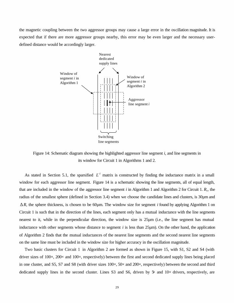
Figure 14: Schematic diagram showing the highlighted aggressor line segment i, and line segments in
its window for Circuit 1 in Algorithms 1 and 2.
As stated in Section 5.1, the sparsified L-1 matrix is constructed by finding the inductance matrix in a small
window for each aggressor line segment. Figure 14 is a schematic showing the line segments, all of equal length,
that are included in the window of the aggressor line segment i in Algorithm 1 and Algorithm 2 for Circuit 1. Rs, the
radius of the smallest sphere (defined in Section 3.4) when we choose the candidate lines and clusters, is 30µm and
∆ R, the sphere thickness, is chosen to be 60µm. The window size for segment i found by applying Algorithm 1 on
Circuit 1 is such that in the direction of the lines, each segment only has a mutual inductance with the line segments
nearest to it, while in the perpendicular direction, the window size is 25µm (i.e., the line segment has mutual
inductance with other segments whose distance to segment i is less than 25µm). On the other hand, the application
of Algorithm 2 finds that the mutual inductances of the nearest line segments and the second nearest line segments
on the same line must be included in the window size for higher accuracy in the oscillation magnitude.
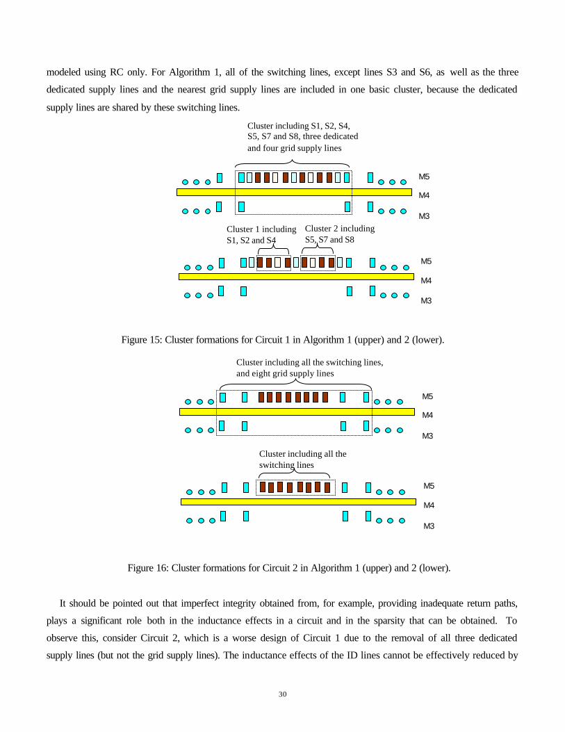
Two basic clusters for Circuit 1 in Algorithm 2 are formed as shown in Figure 15, with S1, S2 and S4 (with
driver sizes of 100×, 200× and 100×, respectively) between the first and second dedicated supply lines being placed
in one cluster, and S5, S7 and S8 (with driver sizes 100×, 50× and 200×, respectively) between the second and third
dedicated supply lines in the second cluster. Lines S3 and S6, driven by 5× and 10× drivers, respectively, are
Aggressor line segment i
Window of segment i in Algorithm 2
Nearest dedicated supply lines
Switching line segments
Window of segment i in Algorithm 1
30
modeled using RC only. For Algorithm 1, all of the switching lines, except lines S3 and S6, as well as the three
dedicated supply lines and the nearest grid supply lines are included in one basic cluster, because the dedicated
supply lines are shared by these switching lines.
Figure 15: Cluster formations for Circuit 1 in Algorithm 1 (upper) and 2 (lower).
Figure 16: Cluster formations for Circuit 2 in Algorithm 1 (upper) and 2 (lower).
It should be pointed out that imperfect integrity obtained from, for example, providing inadequate return paths,
plays a significant role both in the inductance effects in a circuit and in the sparsity that can be obtained. To
observe this, consider Circuit 2, which is a worse design of Circuit 1 due to the removal of all three dedicated
supply lines (but not the grid supply lines). The inductance effects of the ID lines cannot be effectively reduced by
M5 M4 M3
Cluster 1 including S1, S2 and S4
Cluster 2 including S5, S7 and S8
M5 M4 M3
Cluster including S1, S2, S4, S5, S7 and S8, three dedicated and four grid supply lines
M5 M4 M3
Cluster including all the switching lines
M5 M4 M3
Cluster including all the switching lines, and eight grid supply lines

31
supply lines. The oscillation magnitude of the second switching line jumps to 371mV and the 50% delay increases
to 14.2ps. For Algorithm 1, if the same level of accuracy is maintained, the window size in the direction of the lines
increases to two (i.e., each segment has a mutual inductance with the line segments nearest to and the next nearest
to it), and in the perpendicular direction it is 70µm. The clusters formed by Algorithm 1 and 2 for Circuit 2 are
shown in Figure 16. Even the mutual inductance with lines that would have been expected to be highly RD (such as
lines S3 and S6) must be considered for the accurate modeling of the response of RD lines, and a larger number of
grid supply lines must be included into clusters.
7.2 Sparsification comparisons
In this section, we compare the sparsification obtained from Algorithm 1 and the shift-and-truncate method under
the same accuracy for four circuit Circuit 1, 2 3 and 4, summarized in Table 2, which also includes the results from
Algorithm 2.
Circuit 1 Circuit 2 Circuit 3 Circuit 4 Algorithm 1 97% 87% 97% 83% Algorithm 2 99% 98% 98.4% 97%
Shift-and-truncate 92.5% 75% 90% 68%
Table 2: Sparsification from Algorithm 1, Algorithm 2 and the shift-and-truncate method in Circuit 1, 2 3 and 4.
For a good design such as Circuit 1, Algorithm 2 achieves 99% sparsification, while the corresponding figure
for Algorithm 1 is 97%, which is expectedly lower since the latter is the more accurate algorithm. It was found that
for both of our circuit-aware algorithms, the sparsifications for Circuit 2 are worse than those for Circuit 1. For
Algorithm 2, if the sparsification is still relatively high at 98%, the error in the 50% delay reaches 12% and the
error in the oscillation magnitude is larger than 150mV. For Algorithm 1, if we still obtain 15% error in the
oscillation magnitude and 10% error in delay, the sparsification is found to be 87%. Under the same accuracy, the
corresponding sparsification for the shift-and-truncate method was found to be lower, at 75%.
(a) (b)
Figure 17: Cross sectional views of (a) Circuit 3 and (b) Circuit 4.
M5 M4 M3
Signal lines Grid supply lines
Grid supply lines
M5 M4 M3
Signal lines Dedicated supply lines
Dedicated supply lines
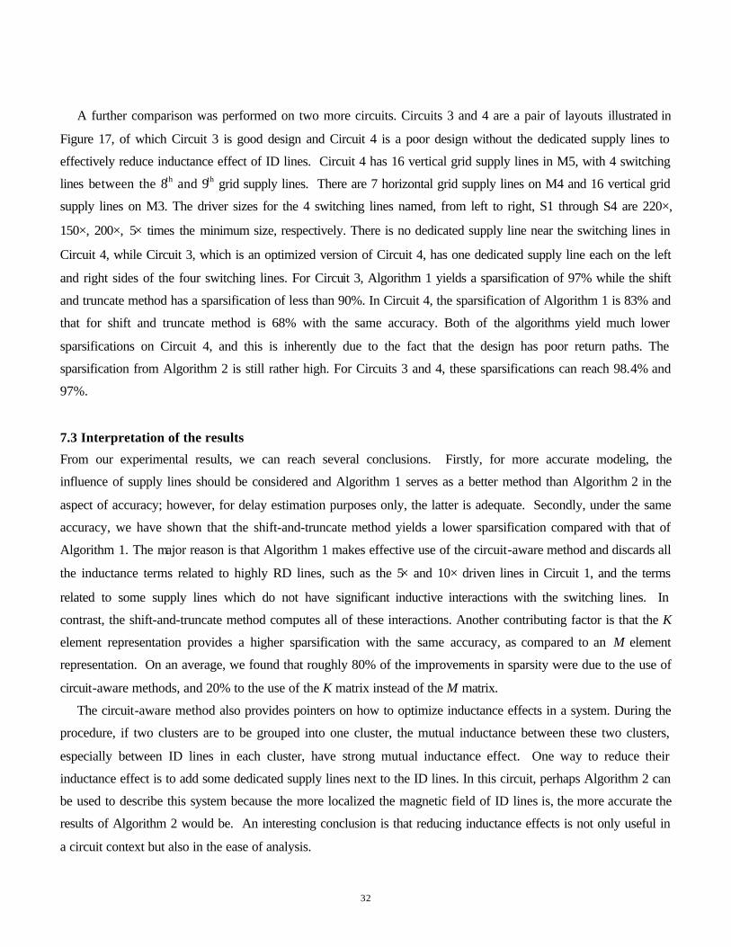
32
A further comparison was performed on two more circuits. Circuits 3 and 4 are a pair of layouts illustrated in
Figure 17, of which Circuit 3 is good design and Circuit 4 is a poor design without the dedicated supply lines to
effectively reduce inductance effect of ID lines. Circuit 4 has 16 vertical grid supply lines in M5, with 4 switching
lines between the 8th and 9th grid supply lines. There are 7 horizontal grid supply lines on M4 and 16 vertical grid
supply lines on M3. The driver sizes for the 4 switching lines named, from left to right, S1 through S4 are 220×,
150×, 200×, 5× times the minimum size, respectively. There is no dedicated supply line near the switching lines in
Circuit 4, while Circuit 3, which is an optimized version of Circuit 4, has one dedicated supply line each on the left
and right sides of the four switching lines. For Circuit 3, Algorithm 1 yields a sparsification of 97% while the shift
and truncate method has a sparsification of less than 90%. In Circuit 4, the sparsification of Algorithm 1 is 83% and
that for shift and truncate method is 68% with the same accuracy. Both of the algorithms yield much lower
sparsifications on Circuit 4, and this is inherently due to the fact that the design has poor return paths. The
sparsification from Algorithm 2 is still rather high. For Circuits 3 and 4, these sparsifications can reach 98.4% and
97%.
7.3 Interpretation of the results
From our experimental results, we can reach several conclusions. Firstly, for more accurate modeling, the
influence of supply lines should be considered and Algorithm 1 serves as a better method than Algorithm 2 in the
aspect of accuracy; however, for delay estimation purposes only, the latter is adequate. Secondly, under the same
accuracy, we have shown that the shift-and-truncate method yields a lower sparsification compared with that of
Algorithm 1. The major reason is that Algorithm 1 makes effective use of the circuit-aware method and discards all
the inductance terms related to highly RD lines, such as the 5× and 10× driven lines in Circuit 1, and the terms
related to some supply lines which do not have significant inductive interactions with the switching lines. In
contrast, the shift-and-truncate method computes all of these interactions. Another contributing factor is that the K
element representation provides a higher sparsification with the same accuracy, as compared to an M element
representation. On an average, we found that roughly 80% of the improvements in sparsity were due to the use of
circuit-aware methods, and 20% to the use of the K matrix instead of the M matrix.
The circuit-aware method also provides pointers on how to optimize inductance effects in a system. During the
procedure, if two clusters are to be grouped into one cluster, the mutual inductance between these two clusters,
especially between ID lines in each cluster, have strong mutual inductance effect. One way to reduce their
inductance effect is to add some dedicated supply lines next to the ID lines. In this circuit, perhaps Algorithm 2 can
be used to describe this system because the more localized the magnetic field of ID lines is, the more accurate the
results of Algorithm 2 would be. An interesting conclusion is that reducing inductance effects is not only useful in
a circuit context but also in the ease of analysis.
33
8. Conclusion
Two circuit-aware based sparsification methodologies for fully coupled PEEC K-element representations for an
inductive system are proposed by analyzing the circuit characteristics and clustering the inductances according to
their relative importance to the circuit. In both algorithms, all of the switching lines are classified as ID or RD lines.
Strong couplings are resolved first and weak couplings are then added to the clusters. Algorithm 2 works with the
assumption of zero ∑j
jij dtdIL )/( drop on the supply lines while Algorithm 1 has no such limitation. Our
experimental results show the effectiveness of the circuit-aware method compared with the shift-and-truncate
method. Algorithm 2 works well in a good design where supply lines behave more perfectly and often gives a high
sparsification but a relatively low accuracy. Algorithm 1 is designed for any circuit and provides a high accuracy
but with a lower sparsification than that of Algorithm 2. The circuit-aware method helps to determine current return
paths for a design and identifies the most critical inductance terms for optimization.

34
References
[1] A. E. Ruehli, “Inductance Calculations in a Complex Integrated Circuit Environment,” IBM Journal of
Research and Development, pp. 470-481, vol. 16, No. 5, September 1972.
[2] F. W. Grover, Inductance calculations: Working Formulas and Tables, Dover Publications, New York, NY,
1946.
[3] B. Krauter and L. T. Pileggi, “Generating Sparse Inductance Matrices with Guaranteed Stability,” Proc. of the
IEEE/ACM International Conference on Computer-Aided Design, pp. 45-52, November 1995.
[4] Z. He, M. Celik and L. T. Pileggi, “SPIE: Sparse Partial Inductance Extraction,” Proc. of the ACM/IEEE Design
Automation Conference, pp. 137-140, June 1997.
[5] M. Beattie, B. Krauter, L. Alatan and L. Pileggi, “Equipotential Shells for Efficient Inductance Extraction,”
IEEE Transactions on Computer-Aided Design of Integrated Circuits & Systems , pp. 70-79, vol. 20, No. 1,
January 2001.
[6] A. J. Dammers and N. P. Van Der Meijs, “Virtual Screening: A Step Towards a Sparse Partial Inductance
Matrix,” Proc. of the IEEE/ACM International Conference on Computer-Aided Design, pp. 445-452,
November 1999.
[7] K. L. Shepard, D. Sitaram and Y. Zheng, “Full-Chip, Three-Dimensional, Shapes-Based RLC Extraction,”
Proc. of the IEEE/ACM International Conference on Computer-Aided Design, pp. 142-149, November 2000.
[8] K. Gala, D. Blaauw, J. Wang, M. Zhao and V. Zolotov, “Inductance 101: Analysis and Design,” Proc. of the
ACM/IEEE Design Automation Conference, pp. 329-334, June 2001.
[9] M. Kamon, M. J. Tsuk and J. White, “FastHenry: A Multipole -Accelerated 3-D Inductance Extraction
Program,” Proc. of the ACM/IEEE Design Automation Conference, pp. 678-683, June 1993.
[10] S. Lin, N. Chang and S. Nakagama, “Quick On-Chip Self- and Mutual-Inductance Screen,” Proc. of the
International Symposium on Quality in Electronic Design, 2000.
[11] L. He, N. Chang, S. Lin and O. S. Nakagama, “An Efficient Inductance Modeling for On-Chip Interconnects,”
Proc. of the IEEE Custom Integrated Circuits Conference, pp. 457-460, May 1999.
[12] H. Smith, A. Deutsch, S. Mehrotra, D. Widiger, M. Bowen, A. Dansky, G. Kopcsay and B. Krauter, “R(f)L(f)C
Coupled Noise Evaluation of an S/390 Microprocessor Chip,” Proc. of the IEEE Custom Integrated Circuits
Conference, pp. 237-240, May 2001.
[13] A. Devgan, H. Ji and W. Dai, “How to Efficiently Capture On-Chip Inductance Effects: Introducing a New
Circuit Element K,” Proc. of the IEEE/ACM International Conference on Computer-Aided Design, pp. 150-
155, November 2000.
[14] H. Ji, A. Devgan and W. Dai, “KSPICE: Efficient and Stable RKC Simulation for Capturing On-Chip
Inductance Effect,” Technical Report UCSC-CRL-00-10, University of California Santa Cruz, Santa Cruz,
CA, 2000. Available at http://ftp.cse.ucsc.edu/pub/tr/ucsc-csl-00-10.ps.Z.

35
[15] A. Odabasioglu, M. Celik and L. T. Pileggi, “PRIMA: Passive Reduced-Order Interconnect Macromodeling
Algorithm,” Proc. of the IEEE/ACM International Conference on Computer-Aided Design, pp. 58-65,
November 1997.
[16] J. H. Chern, J. Huang, L. Arledge, P-C Li and P. Yang, “Multilevel Metal Capacitance Models for CAD
Design Synthesis Systems,” IEEE Electron Device Letters, vol. 13, No. 1, pp. 32-34, January 1992.
[17] J. Cong, “Challenges and Opportunities for Design Innovations in Nanometer Technologies,” SRC Design
Science Concept Paper, 1997.
[18] A. E. Ruehli, Circuit Analysis, Simulation and Design, vol. 3, Part 2, North-Holland, Amsterdam, The
Netherlands, 1987.