Embed Size (px)
Citation preview
1Shen Lin
ASIC/SOC 2000 Interconnect Modeling and Design for Giga-Hertz Circuits and Systems
Hewlett [email protected]
On-Chip Inductance and Coupling Effects
Shen Lin
Hewlett Packard Labs.
2Shen Lin
ASIC/SOC 2000 Interconnect Modeling and Design for Giga-Hertz Circuits and Systems
Hewlett [email protected]
Outline
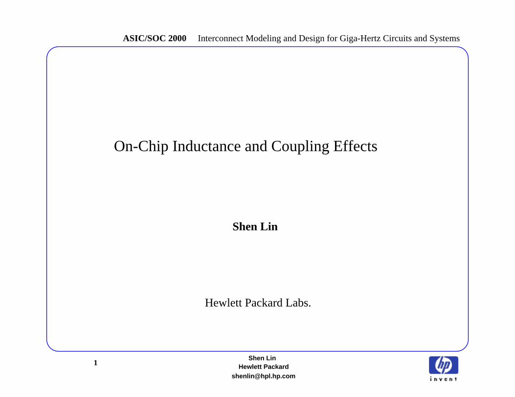
1. Introduction
3. Significant Frequency of High-Speed Pulse
2. Differences in On-Chip Inductance Consideration
4. Inductance Calculations
5. Proximity and Skin Effects
6. Circuit Modeling and Inductance Impacts7. Self-Inductance Screening Rules
8. Mutual-Inductance Screening Rules
9. Efficient Inductance Modelings
10. Inductance Test Chip Benchmark
11. Techniques to Minimize Inductance Effects
3Shen Lin
ASIC/SOC 2000 Interconnect Modeling and Design for Giga-Hertz Circuits and Systems
Hewlett [email protected]
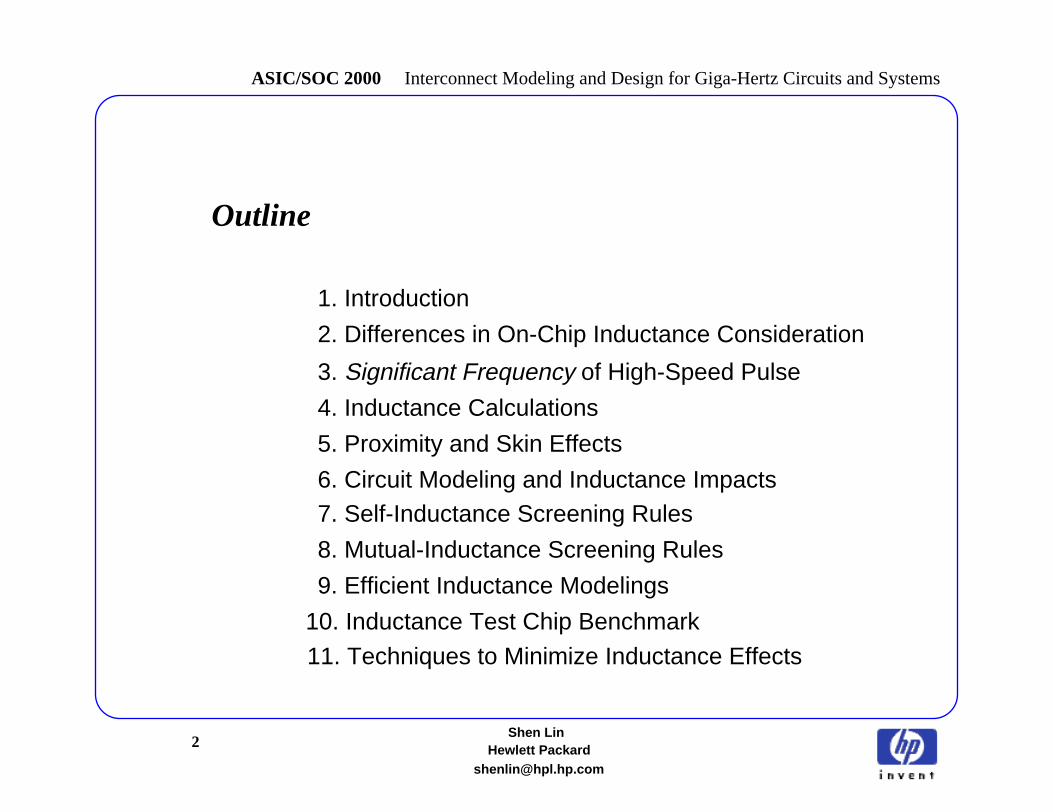
Introduction
On-Chip Inductance effects have become increasingly significant
because:
1) For performance considerations, some global signal and clock
wires are routed with large widths and thicknesses at the top levels
of the metal to minimize delays. This decreases the resistance of
the wires, making their inductive impedance comparable to the
resistive part.
There is more to impedance than resistance:Z R jωL+=
WhenωL is comparable to R, inductive effects must be considered..

4Shen Lin
ASIC/SOC 2000 Interconnect Modeling and Design for Giga-Hertz Circuits and Systems
Hewlett [email protected]
L nH( ) 2l2l
w t+------------
ln 0.5 k–+×=
Resistance and inductive reactance ofAl wires at 1GHz for different lengthsand widths.
Partial-Self-Inductance Increases Super-linearly:
5Shen Lin
ASIC/SOC 2000 Interconnect Modeling and Design for Giga-Hertz Circuits and Systems
Hewlett [email protected]
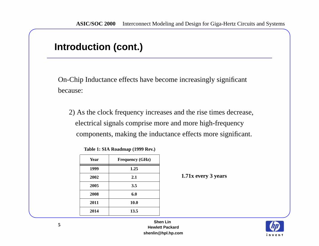
Introduction (cont.)
On-Chip Inductance effects have become increasingly significant
because:
2) As the clock frequency increases and the rise times decrease,
electrical signals comprise more and more high-frequency
components, making the inductance effects more significant.
Table 1: SIA Roadmap (1999 Rev.)
Year Frequency (GHz)
1999 1.25
2002 2.1
2005 3.5
2008 6.0
2011 10.0
2014 13.5
1.71x every 3 years
6Shen Lin
ASIC/SOC 2000 Interconnect Modeling and Design for Giga-Hertz Circuits and Systems
Hewlett [email protected]
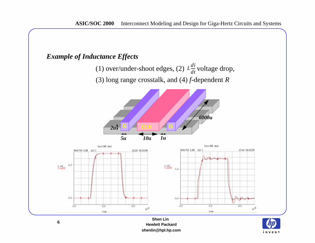
CLK GG
Example of Inductance Effects
6000u
2u
10u5u 1u
(3) long range crosstalk, and (4)f-dependentR
Ldidt-----(1) over/under-shoot edges, (2) voltage drop,
7Shen Lin
ASIC/SOC 2000 Interconnect Modeling and Design for Giga-Hertz Circuits and Systems
Hewlett [email protected]
Introduction (cont.)
On-Chip Inductance effects have become increasingly significant
because:
4) With the push of performance, some low-resistivity metals,
e.g.Cu wires, have been explored to replaceAl in order to
minimize wireRC delays. This could make the wire inductive
reactance larger than the resistance.
3) With the increase of chip size, it is fairly typical that many wire
are long and run in parallel, which increases the inductive
crosstalk and delay.

8Shen Lin
ASIC/SOC 2000 Interconnect Modeling and Design for Giga-Hertz Circuits and Systems
Hewlett [email protected]
Differences in On-Chip Inductance Consideration
1. The internal inductance of on-chip wires needs to be considered
because the skin depths at the frequencies that we consider arecomparable to the wire thickness or width. Most electrical currents
flow inside the wires.
G 1 2
5u 5u
1.9u 5000u
L̃1
c2-----C̃ 1–=
Frequency RI3 RC2 % difference
1 GHz 23%
100 GHz 15%
10,000 GHz 10%
3.7689–×10 2.563
9–×10
2.5639–×10 5.125
9–×10
2.9839–×10 2.133
9–×10
2.1339–×10 4.266
9–×10
3.5389–×10 2.425
9–×10
2.4259–×10 4.850
9–×10
2.9839–×10 2.133
9–×10
2.1339–×10 4.266
9–×10
3.2039–×10 2.233
9–×10
2.2339–×10 4.626
9–×10
2.9839–×10 2.133
9–×10
2.1339–×10 4.266
9–×10
Inductance is calculated by
in RC2.

9Shen Lin
ASIC/SOC 2000 Interconnect Modeling and Design for Giga-Hertz Circuits and Systems
Hewlett [email protected]
Differences in On-Chip Inductance Consideration
2. Due to the lack of highly conductive ground plane on chip,
the mutual couplings between wires cover very long rangesand decrease very slowly with the increase of spacing.
Spacing K12 of (a) compared with1um-spacing K12 of (b) compared with
1um-spacing
1u 0.73 100% 0.29 100%
10u 0.57 78% 0.034 11%
50u 0.54 74% 0.0059 2.0%
100u 0.53 72% 0.0038 1.3%
G 1 25u
2000u 0 1 2
5u
1.9u 2000u
spacingspacing
(a) (b)
1.2u
ground plane
10Shen Lin
ASIC/SOC 2000 Interconnect Modeling and Design for Giga-Hertz Circuits and Systems
Hewlett [email protected]
Why the silicon substrate cannot be considered as a ground plane?
1. The resistivity of the lightly doped substrate layer is
about two million times larger than aluminum.
2. The substrate is too far away from the high-speed
buses or clock wires.
11Shen Lin
ASIC/SOC 2000 Interconnect Modeling and Design for Giga-Hertz Circuits and Systems
Hewlett [email protected]
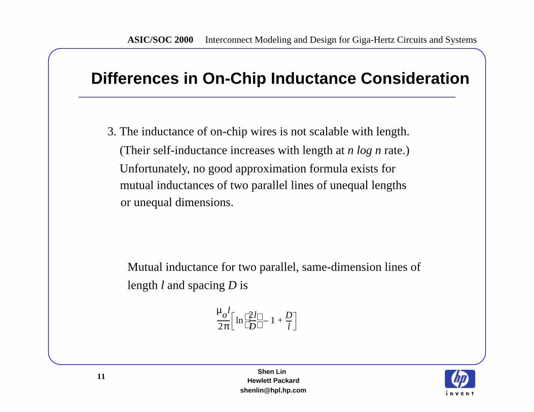
Differences in On-Chip Inductance Consideration
3. The inductance of on-chip wires is not scalable with length.
(Their self-inductance increases with length atn log n rate.)
Unfortunately, no good approximation formula exists formutual inductances of two parallel lines of unequal lengths
or unequal dimensions.
Mutual inductance for two parallel, same-dimension lines of
lengthl and spacingD is
µol
2π-------- 2l
D-----
ln 1– Dl----+
12Shen Lin
ASIC/SOC 2000 Interconnect Modeling and Design for Giga-Hertz Circuits and Systems
Hewlett [email protected]
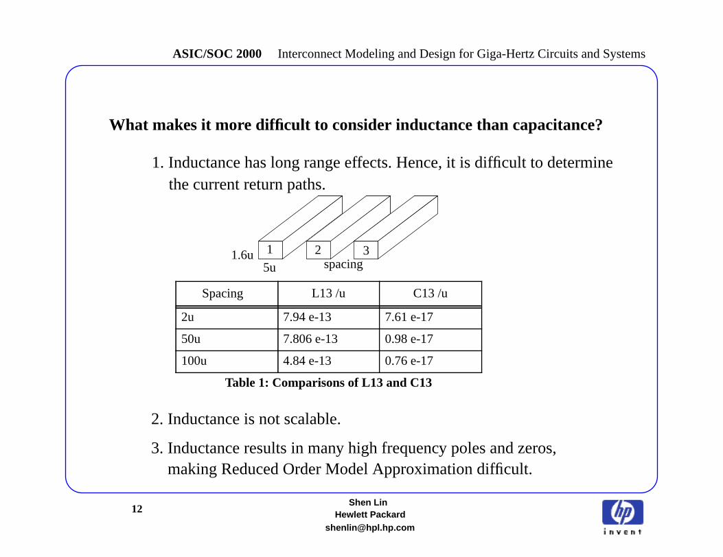
What makes it more difficult to consider inductance than capacitance?
1. Inductance has long range effects. Hence, it is difficult to determine
L13 /u C13 /u
2u 7.94 e-13 7.61 e-17
50u 7.806 e-13 0.98 e-17
100u 4.84 e-13 0.76 e-17
Table 1: Comparisons of L13 and C13
Spacing
5u1.6u 1 2 3
spacing
3. Inductance results in many high frequency poles and zeros, making Reduced Order Model Approximation difficult.
2. Inductance is not scalable.
the current return paths.
13Shen Lin
ASIC/SOC 2000 Interconnect Modeling and Design for Giga-Hertz Circuits and Systems
Hewlett [email protected]
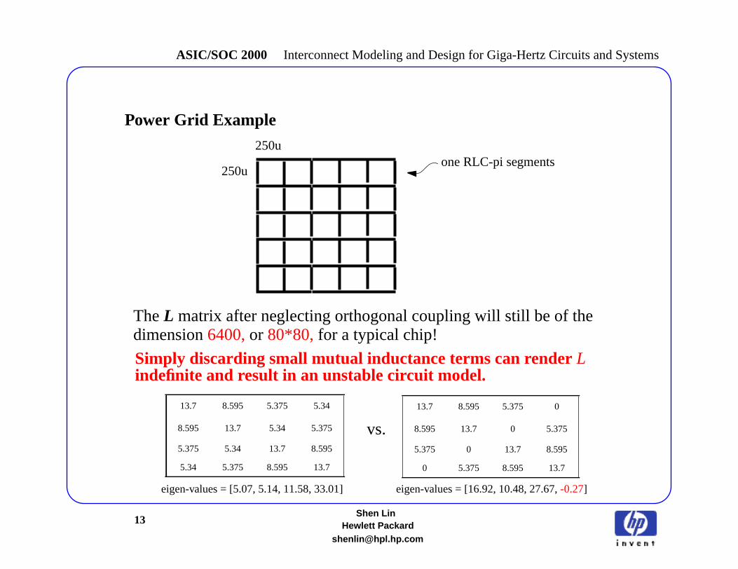
Power Grid Example
one RLC-pi segments250u
250u
TheL matrix after neglecting orthogonal coupling will still be of the
Simply discarding small mutual inductance terms can renderLindefinite and result in an unstable circuit model.
dimension6400,or 80*80, for a typical chip!
13.7 8.595 5.375 5.34
8.595 13.7 5.34 5.375
5.375 5.34 13.7 8.595
5.34 5.375 8.595 13.7
eigen-values = [5.07, 5.14, 11.58, 33.01]
13.7 8.595 5.375 0
8.595 13.7 0 5.375
5.375 0 13.7 8.595
0 5.375 8.595 13.7
eigen-values = [16.92, 10.48, 27.67,-0.27]
vs.

14Shen Lin
ASIC/SOC 2000 Interconnect Modeling and Design for Giga-Hertz Circuits and Systems
Hewlett [email protected]
G 1 2 3 4 5 6
5u
1.9u
5u
w/ consideration of L w/o consideration of L
15Shen Lin
ASIC/SOC 2000 Interconnect Modeling and Design for Giga-Hertz Circuits and Systems
Hewlett [email protected]
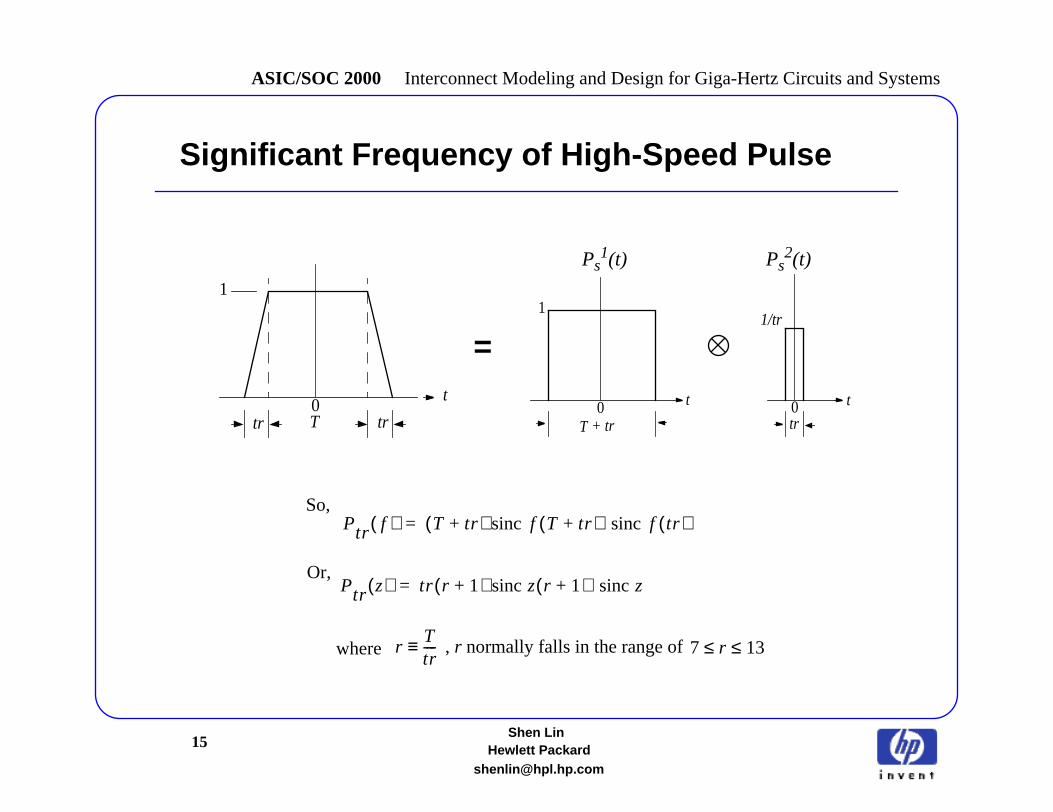
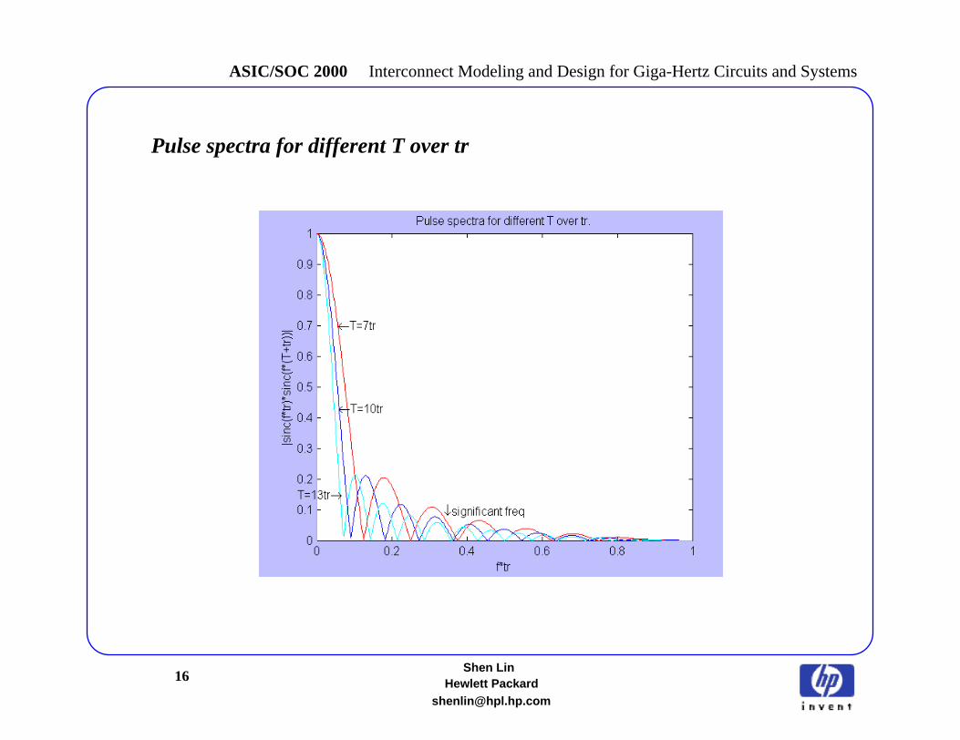
Significant Frequency of High-Speed Pulse
Ttr tr
t
1
0T + tr
t
1
0tr
1/tr
0 t
Ps1(t) Ps
2(t)
=
Ptr f( ) T tr+( ) sinc f T tr+( ) sinc f tr( )=
Ptr z( ) tr r 1+( ) sinc z r 1+( ) sinc z=
rTtr----≡ 7 r 13≤ ≤
So,
Or,
where , r normally falls in the range of
16Shen Lin
ASIC/SOC 2000 Interconnect Modeling and Design for Giga-Hertz Circuits and Systems
Hewlett [email protected]
Pulse spectra for different T over tr
17Shen Lin
ASIC/SOC 2000 Interconnect Modeling and Design for Giga-Hertz Circuits and Systems
Hewlett [email protected]
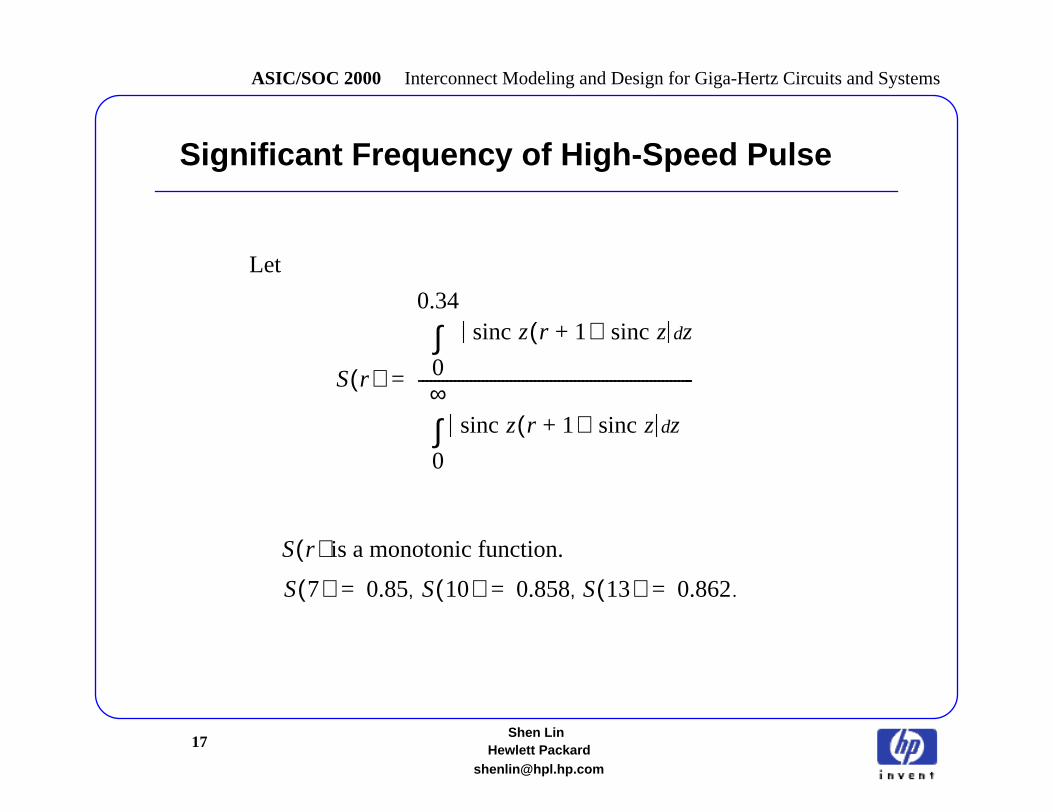
Significant Frequency of High-Speed Pulse
S r( )
sinc z r 1+( ) sinc z zd
0
0.34
∫
sinc z r 1+( ) sinc z zd
0
∞
∫
---------------------------------------------------------------------=
S 7( ) 0.85,=
S r( )
S 13( ) 0.862.=
is a monotonic function.
Let
S 10( ) 0.858,=
18Shen Lin
ASIC/SOC 2000 Interconnect Modeling and Design for Giga-Hertz Circuits and Systems
Hewlett [email protected]
Significant Frequency of High-Speed Pulse
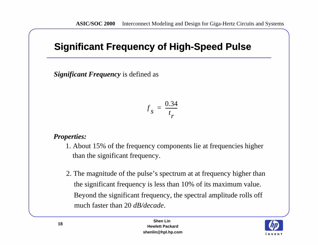
f s0.34tr
----------=
Significant Frequency is defined as
Properties:1. About 15% of the frequency components lie at frequencies higher
than the significant frequency.
2. The magnitude of the pulse’s spectrum at at frequency higher than
the significant frequency is less than 10% of its maximum value.
Beyond the significant frequency, the spectral amplitude rolls off
Significant Frequency of High-Speed Pulse
much faster than 20dB/decade.
19Shen Lin
ASIC/SOC 2000 Interconnect Modeling and Design for Giga-Hertz Circuits and Systems
Hewlett [email protected]
Inductance Calculation
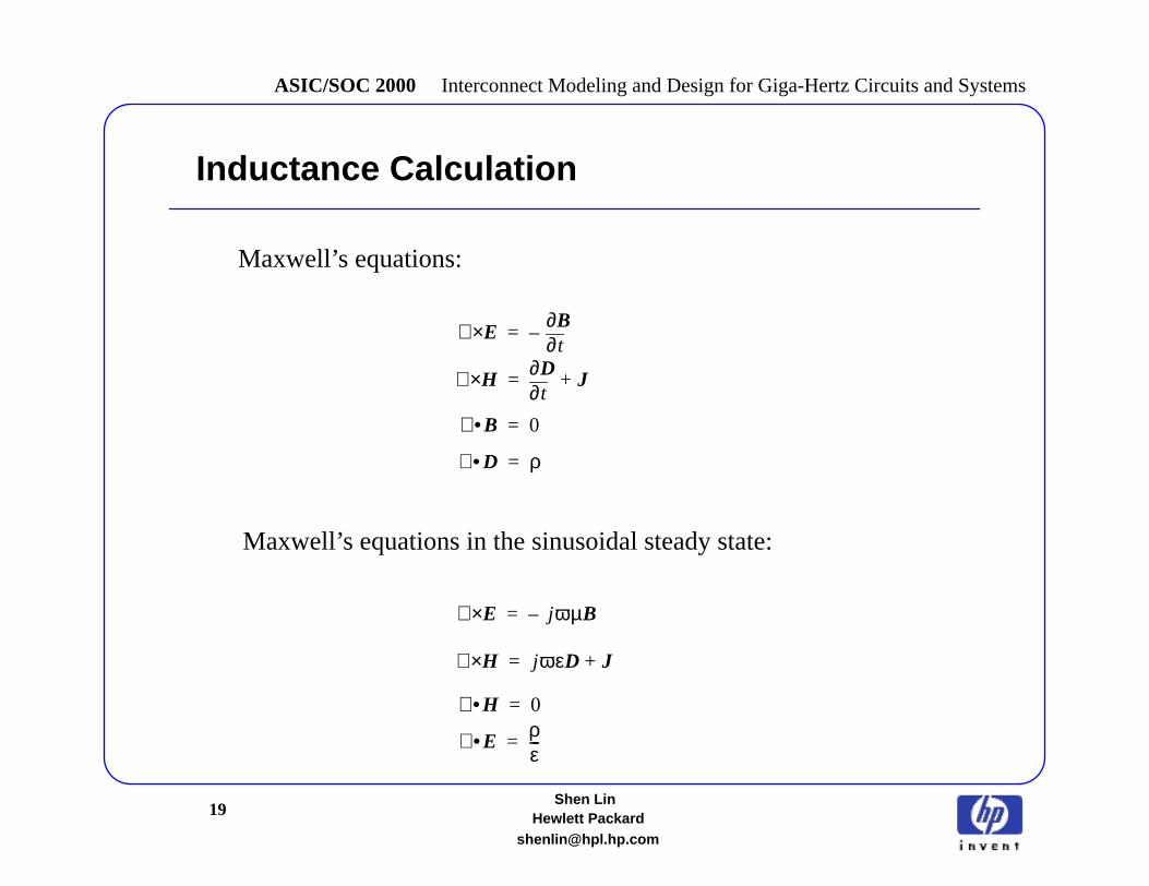
E∇×t∂
∂B–=
B∇• 0=
H∇×t∂
∂D J+=
D∇• ρ=
Maxwell’s equations:
Maxwell’s equations in the sinusoidal steady state:
E∇× jωµB–=
H∇• 0=
H∇× jωεD J+=
E∇• ρε---=
20Shen Lin
ASIC/SOC 2000 Interconnect Modeling and Design for Giga-Hertz Circuits and Systems
Hewlett [email protected]
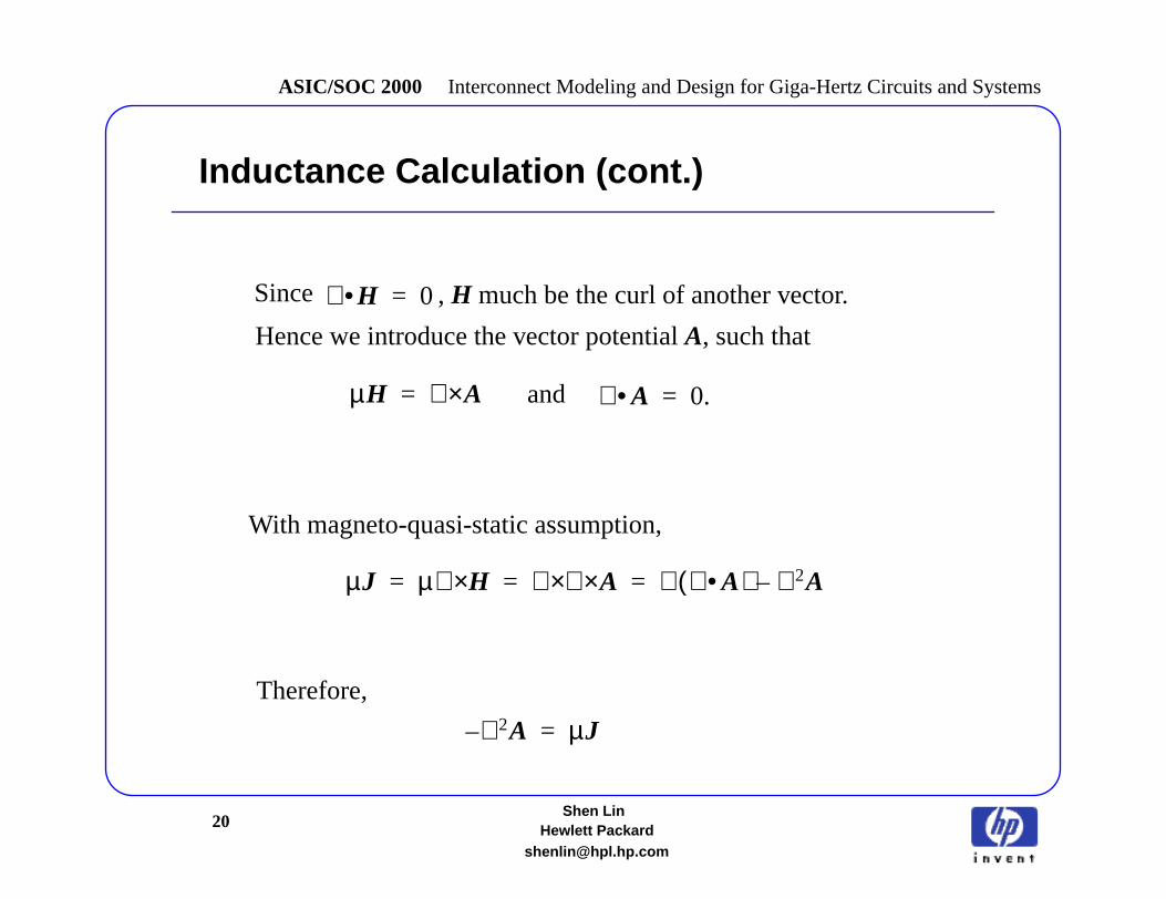
H∇• 0=
µH A∇×=
Inductance Calculation (cont.)
Since , H much be the curl of another vector.
Hence we introduce the vector potentialA, such that
and A∇• 0.=
With magneto-quasi-static assumption,
µJ µ H∇× A∇×∇× A∇•( )∇ A∇2–= = =
A∇2– µJ=
Therefore,
21Shen Lin
ASIC/SOC 2000 Interconnect Modeling and Design for Giga-Hertz Circuits and Systems
Hewlett [email protected]
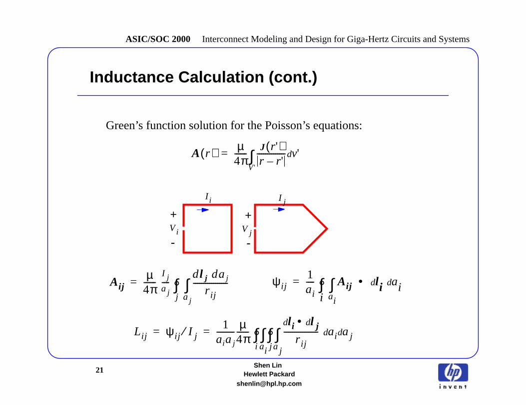
A r( ) µ4π------ J r '( )
r r '–-------------- v'd
V'∫=
Inductance Calculation (cont.)
Green’s function solution for the Poisson’s equations:
+
-
I i I j
V jVi
+
-
Aijµ4π------
I j
a j----
dl j daj
r ij-----------------
aj
∫j∫°=
Lij ψ ij I j⁄ 1aiaj--------- µ
4π------
l i l jd•d
r ij----------------- aid ajd
aj
∫j∫°
ai
∫i∫°= =
ψ ij1ai---- Aij • l i aidd
ai
∫i∫°=
22Shen Lin
ASIC/SOC 2000 Interconnect Modeling and Design for Giga-Hertz Circuits and Systems
Hewlett [email protected]
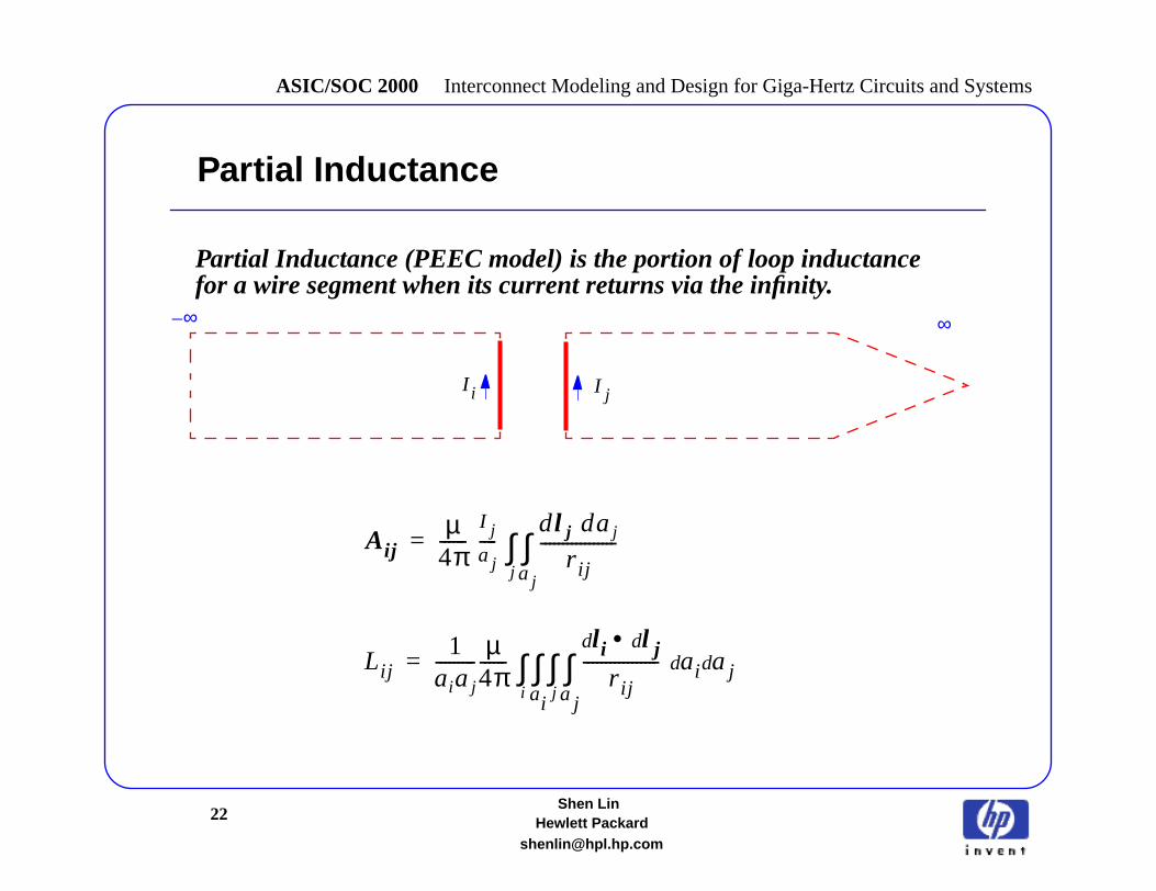
Partial Inductance (PEEC model) is the portion of loop inductance
I i I j
∞∞–
Partial Inductance
Aijµ4π------
I j
a j----
dl j daj
r ij-----------------
aj
∫j∫=
Lij1
aiaj--------- µ
4π------
l i l jd•d
r ij----------------- aid ajd
aj
∫j∫
ai
∫i∫=
for a wire segment when its current returns via the infinity.

23Shen Lin
ASIC/SOC 2000 Interconnect Modeling and Design for Giga-Hertz Circuits and Systems
Hewlett [email protected]
Partial Inductance calculation of an interconnect divided into multiple
Partial Inductance Calculation
Lijµ4π------ 1
akam------------
lkd lmd•r km
--------------------- ak amdd
am
∫bm
cm
∫ak
∫bk
ck
∫m 1=
M
∑k 1=
K
∑=
segments, each of which is a bundle of multiple filaments:
24Shen Lin
ASIC/SOC 2000 Interconnect Modeling and Design for Giga-Hertz Circuits and Systems
Hewlett [email protected]
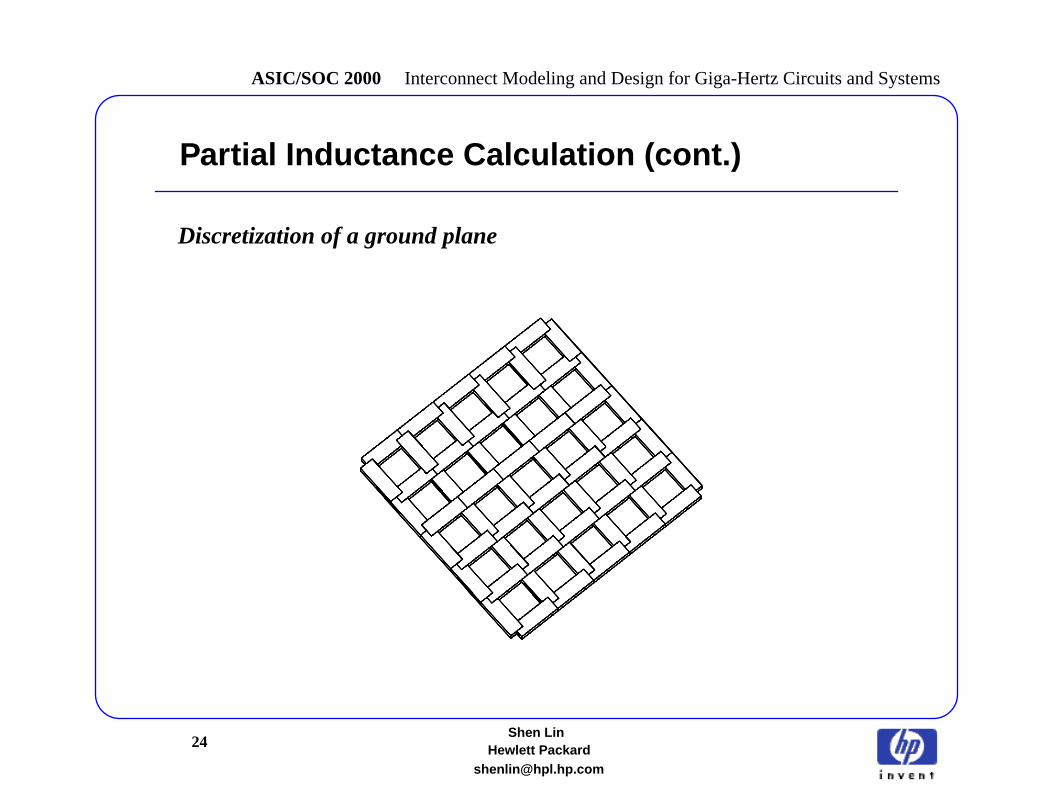
Discretization of a ground plane
Partial Inductance Calculation (cont.)
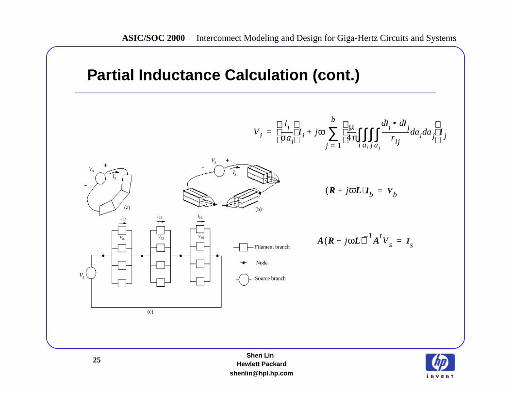
25Shen Lin
ASIC/SOC 2000 Interconnect Modeling and Design for Giga-Hertz Circuits and Systems
Hewlett [email protected]
Partial Inductance Calculation (cont.)
Filament branch
Node
Source branch
(a) (b)
(c)
Vs
Vs
Vs
Ib1Ib5 Ib9
Vb9Vb5Vb1
IsIs
Vi
l iσai--------
I i jω µ4π------
l id l jd•r ij
------------------ ai ajdd
aj
∫j∫
ai
∫i∫
I jj 1=
b
∑+=
R jωL+( ) I b Vb=
A R jωL+( ) 1–A
tVs I s=
26Shen Lin
ASIC/SOC 2000 Interconnect Modeling and Design for Giga-Hertz Circuits and Systems
Hewlett [email protected]
Properties of Partial Inductance
1. Partial self- and mutual- inductances are based on geometry only.
2. They may be solved by using a 2D/3D field solver such as Avanti’s
Raphael or MIT’s FastHenry.
3. The return path or the current loop may be determined through
SPICE simulations.
4. The partial self- and mutual- inductancesmay be frequency- and
proximity- dependent.

27Shen Lin
ASIC/SOC 2000 Interconnect Modeling and Design for Giga-Hertz Circuits and Systems
Hewlett [email protected]
Proximity Effects
vs.
Depending on how the current flows among wires (flow directionsandcurrent distributions ) at differentfrequencies, the current densities
are different. This changes each wire’s impedance, including resistance
and inductance, at different frequencies.
28Shen Lin
ASIC/SOC 2000 Interconnect Modeling and Design for Giga-Hertz Circuits and Systems
Hewlett [email protected]
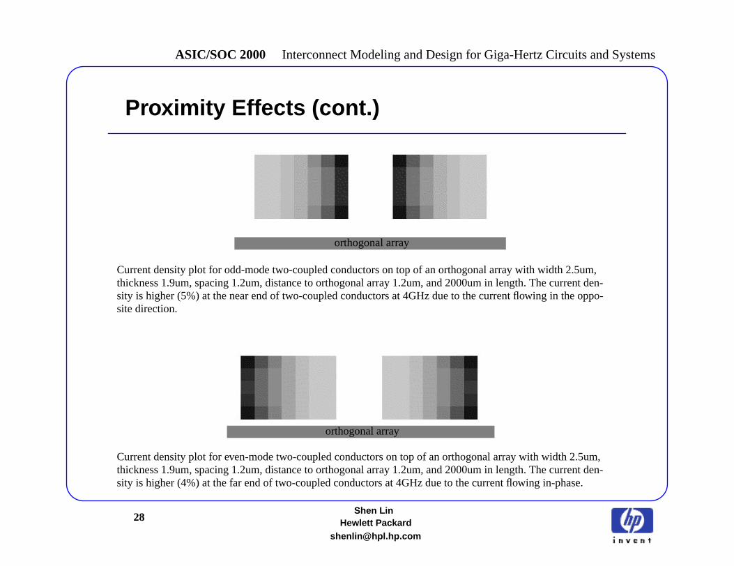
Proximity Effects (cont.)
Current density plot for odd-mode two-coupled conductors on top of an orthogonal array with width 2.5um,thickness 1.9um, spacing 1.2um, distance to orthogonal array 1.2um, and 2000um in length. The current den-sity is higher (5%) at the near end of two-coupled conductors at 4GHz due to the current flowing in the oppo-site direction.
orthogonal array
orthogonal array
Current density plot for even-mode two-coupled conductors on top of an orthogonal array with width 2.5um,thickness 1.9um, spacing 1.2um, distance to orthogonal array 1.2um, and 2000um in length. The current den-sity is higher (4%) at the far end of two-coupled conductors at 4GHz due to the current flowing in-phase.
29Shen Lin
ASIC/SOC 2000 Interconnect Modeling and Design for Giga-Hertz Circuits and Systems
Hewlett [email protected]
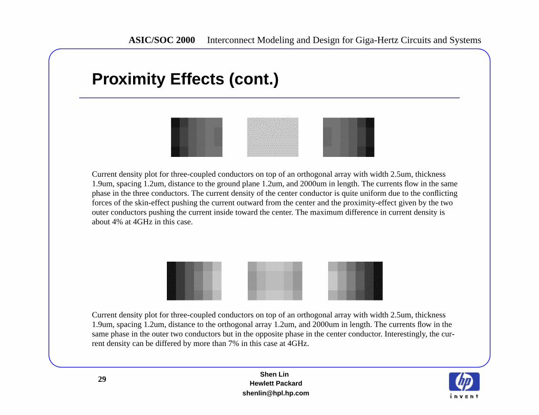
Proximity Effects (cont.)
Current density plot for three-coupled conductors on top of an orthogonal array with width 2.5um, thickness1.9um, spacing 1.2um, distance to the ground plane 1.2um, and 2000um in length. The currents flow in the samephase in the three conductors. The current density of the center conductor is quite uniform due to the conflictingforces of the skin-effect pushing the current outward from the center and the proximity-effect given by the twoouter conductors pushing the current inside toward the center. The maximum difference in current density isabout 4% at 4GHz in this case.
Current density plot for three-coupled conductors on top of an orthogonal array with width 2.5um, thickness1.9um, spacing 1.2um, distance to the orthogonal array 1.2um, and 2000um in length. The currents flow in thesame phase in the outer two conductors but in the opposite phase in the center conductor. Interestingly, the cur-rent density can be differed by more than 7% in this case at 4GHz.
30Shen Lin
ASIC/SOC 2000 Interconnect Modeling and Design for Giga-Hertz Circuits and Systems
Hewlett [email protected]
Proximity Effects (cont.)
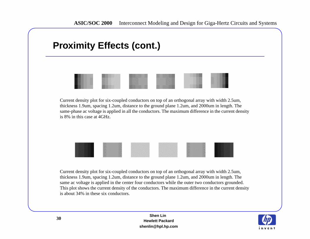
Current density plot for six-coupled conductors on top of an orthogonal array with width 2.5um,thickness 1.9um, spacing 1.2um, distance to the ground plane 1.2um, and 2000um in length. Thesame-phase ac voltage is applied in all the conductors. The maximum difference in the current densityis 8% in this case at 4GHz.
Current density plot for six-coupled conductors on top of an orthogonal array with width 2.5um,thickness 1.9um, spacing 1.2um, distance to the ground plane 1.2um, and 2000um in length. Thesame ac voltage is applied in the center four conductors while the outer two conductors grounded.This plot shows the current density of the conductors. The maximum difference in the current densityis about 34% in these six conductors.
31Shen Lin
ASIC/SOC 2000 Interconnect Modeling and Design for Giga-Hertz Circuits and Systems
Hewlett [email protected]
Skin Effects
Ez E0ex δ⁄–
ejx δ⁄–
=
Jz J0ex δ⁄–
ejx δ⁄–
=
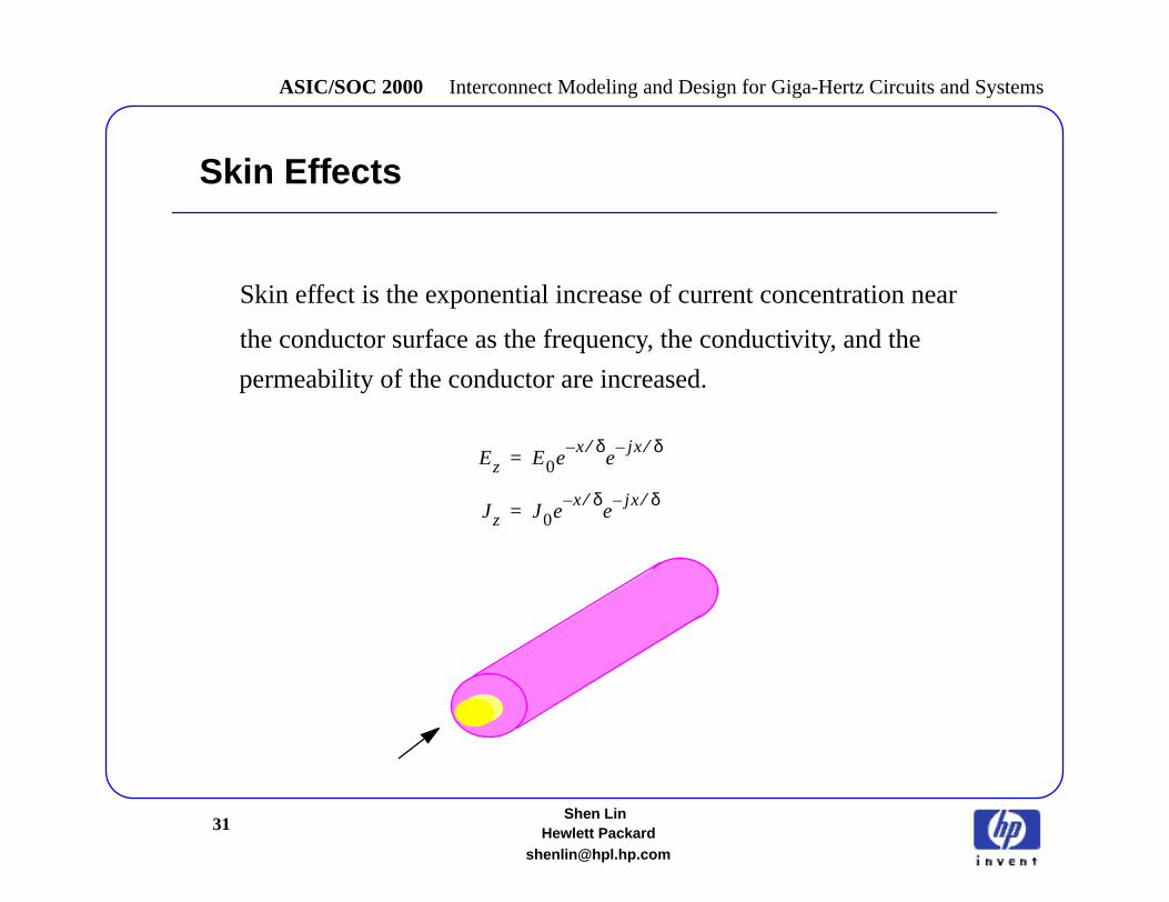
Skin effect is the exponential increase of current concentration near
permeability of the conductor are increased.
the conductor surface as the frequency, the conductivity, and the

32Shen Lin
ASIC/SOC 2000 Interconnect Modeling and Design for Giga-Hertz Circuits and Systems
Hewlett [email protected]
Skin Depth
δ 1
πfµσ-----------------=
The skin depth is the depth of penetration into the conductor
conductivity
permeability
at which the magnitudes of the field and the current decrease
to 1/e (about 36.9%).
33Shen Lin
ASIC/SOC 2000 Interconnect Modeling and Design for Giga-Hertz Circuits and Systems
Hewlett [email protected]
Skin Effects (cont.)
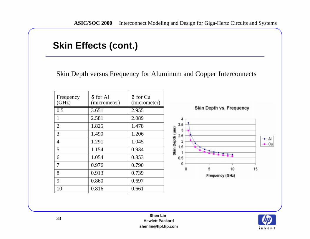
Frequency(GHz)
for Al(micrometer)
for Cu(micrometer)
0.5 3.651 2.955
1 2.581 2.089
2 1.825 1.478
3 1.490 1.206
4 1.291 1.045
5 1.154 0.934
6 1.054 0.853
7 0.976 0.790
8 0.913 0.739
9 0.860 0.697
10 0.816 0.661
δ δ
Skin Depth versus Frequency for Aluminum and Copper Interconnects
34Shen Lin
ASIC/SOC 2000 Interconnect Modeling and Design for Giga-Hertz Circuits and Systems
Hewlett [email protected]
Skin Effects (cont.)
w w w
Frequency Increases
t
w w w
Frequency Increases
Ground Ground Ground
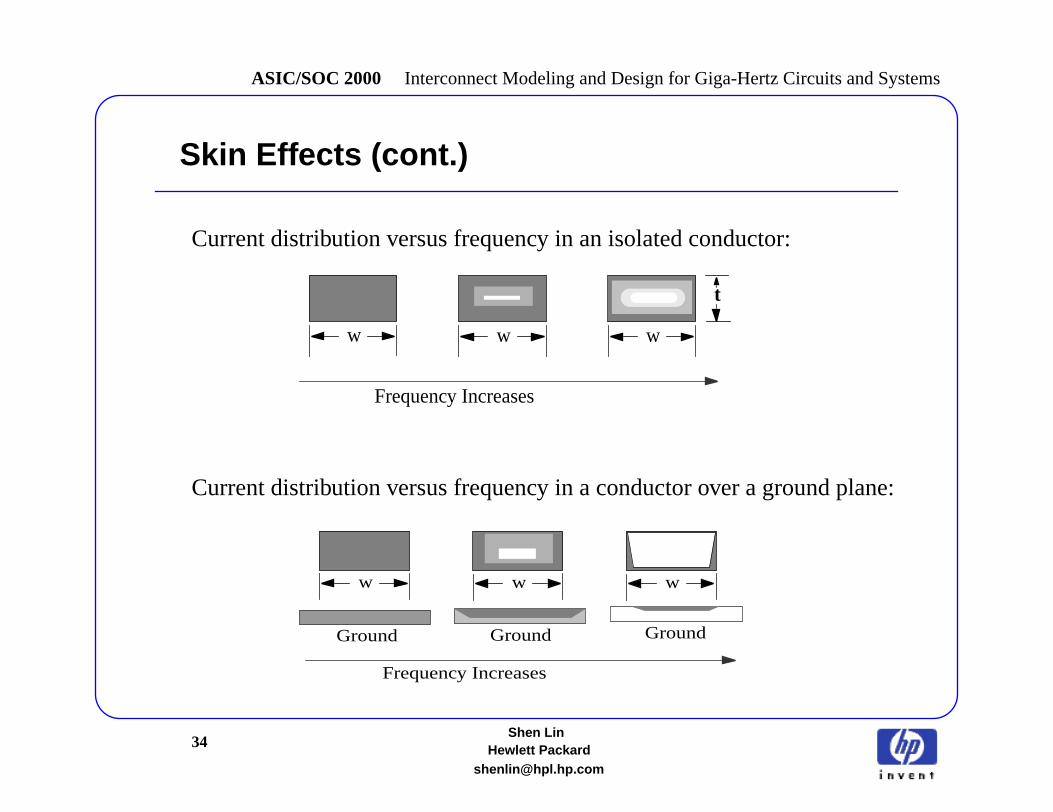
Current distribution versus frequency in an isolated conductor:
Current distribution versus frequency in a conductor over a ground plane:

35Shen Lin
ASIC/SOC 2000 Interconnect Modeling and Design for Giga-Hertz Circuits and Systems
Hewlett [email protected]
Cope with Proximity and Skin Effects using PEEC
Ground Groundsignal signal signal signal
0.1pF 0.1pF 0.1pF 0.1pF0.1ohm
Vs1 Vs2 Vs3 Vs41v 1v 1v 1vVs1 0v Vs1 0v50ohm 50ohm 50ohm 50ohm 0.01ohm0.01ohm
Multiple single bar composition of each rectangular conductor in Raphael RI3 is used to model the skin-effectand proximity-effect induced current density on the six conductor case, for example. Current value is moni-tored during SPICE simulation of the formulated RLC deck of this six conductor case. All the other examplessuch as two conductors or three conductors are modeled and simulated in a similar fashion. In this case, thecurrent density is monitored at the far end of the conductors.
By using fine filament approximations of wires. So, it is a trade-off
between CPU time spent on SPICE simulations and accuracy.
36Shen Lin
ASIC/SOC 2000 Interconnect Modeling and Design for Giga-Hertz Circuits and Systems
Hewlett [email protected]
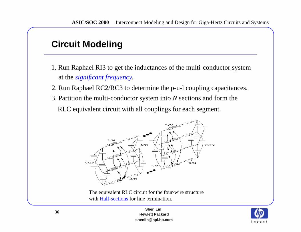
Circuit Modeling
The equivalent RLC circuit for the four-wire structurewith Half-sections for line termination.
1. Run Raphael RI3 to get the inductances of the multi-conductor system
2. Run Raphael RC2/RC3 to determine the p-u-l coupling capacitances.
3. Partition the multi-conductor system intoN sections and form the
RLC equivalent circuit with all couplings for each segment.
at thesignificant frequency.
37Shen Lin
ASIC/SOC 2000 Interconnect Modeling and Design for Giga-Hertz Circuits and Systems
Hewlett [email protected]
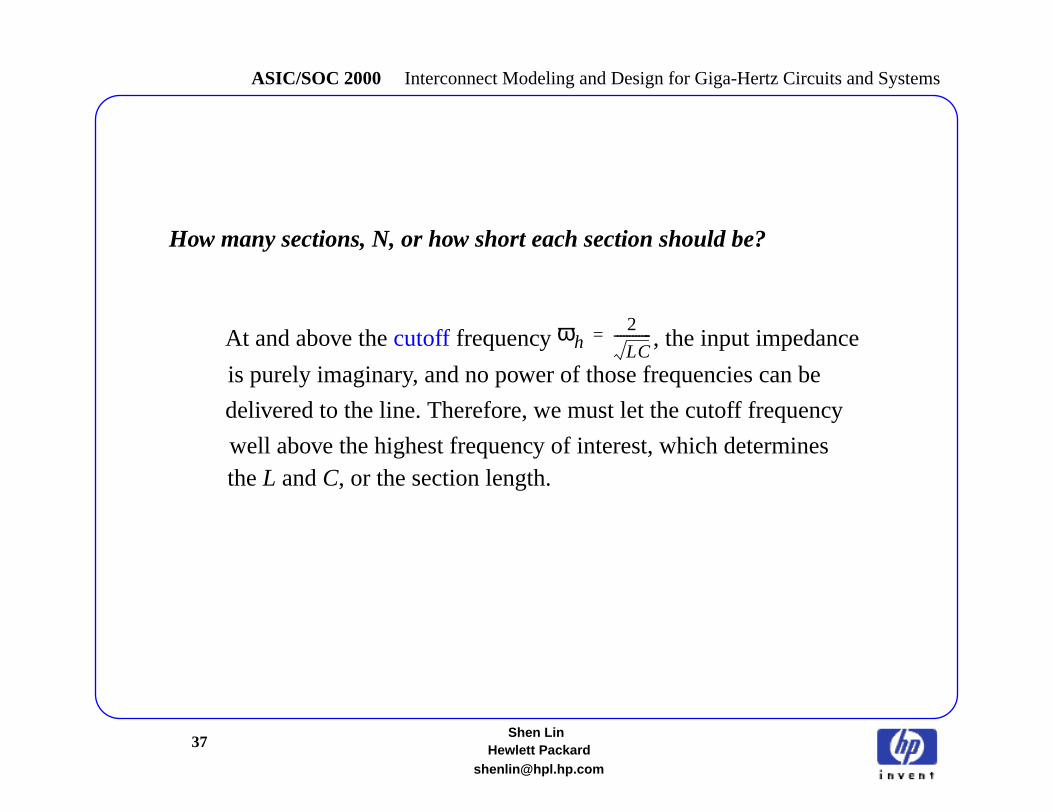
How many sections, N, or how short each section should be?
At and above thecutoff frequency , the input impedance
is purely imaginary, and no power of those frequencies can be
ωh2
LC------------=
delivered to the line. Therefore, we must let the cutoff frequency
well above the highest frequency of interest, which determinestheL andC, or the section length.
38Shen Lin
ASIC/SOC 2000 Interconnect Modeling and Design for Giga-Hertz Circuits and Systems
Hewlett [email protected]
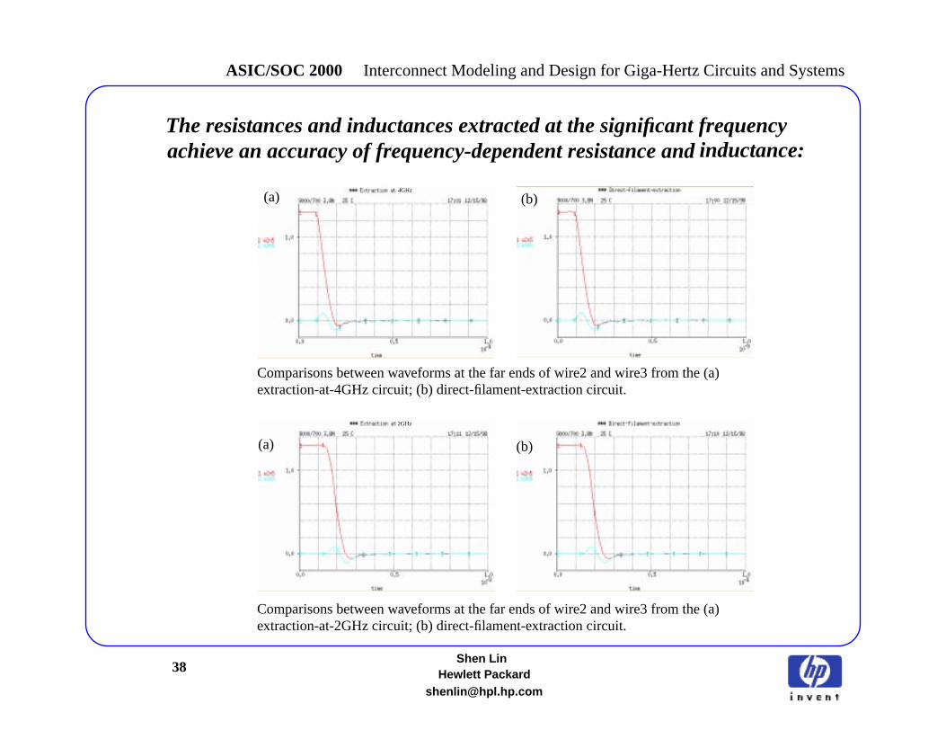
Comparisons between waveforms at the far ends of wire2 and wire3 from the (a)extraction-at-2GHz circuit; (b) direct-filament-extraction circuit.
Comparisons between waveforms at the far ends of wire2 and wire3 from the (a)extraction-at-4GHz circuit; (b) direct-filament-extraction circuit.
(a) (b)
(a) (b)
2GHz
4GHz
The resistances and inductances extracted at the significant frequencyinductance:achieve an accuracy of frequency-dependent resistance and
39Shen Lin
ASIC/SOC 2000 Interconnect Modeling and Design for Giga-Hertz Circuits and Systems
Hewlett [email protected]
Circuit Modeling (cont.)
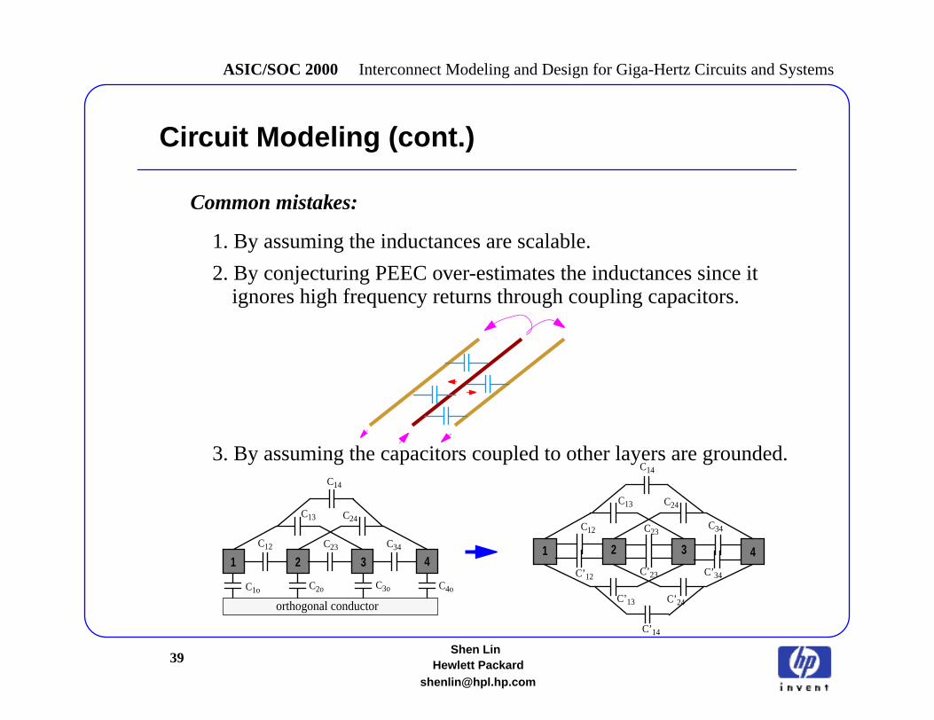
Common mistakes:
1. By assuming the inductances are scalable.
2. By conjecturing PEEC over-estimates the inductances since it
3. By assuming the capacitors coupled to other layers are grounded.
1 2 3 4C12
C14
C13
C34
C24
C23
C3oC2oC1o C4o
orthogonal conductor
1 2 3 4
C14
C13 C24
C12 C23C34
C’14
C’13 C’24
C’12 C’23 C’34
ignores high frequency returns through coupling capacitors.
40Shen Lin
ASIC/SOC 2000 Interconnect Modeling and Design for Giga-Hertz Circuits and Systems
Hewlett [email protected]
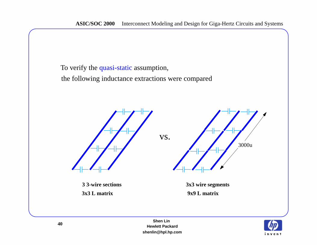
To verify thequasi-static assumption,
vs.
the following inductance extractions were compared
3 3-wire sections 3x3 wire segments
3x3 L matrix 9x9 L matrix
3000u
41Shen Lin
ASIC/SOC 2000 Interconnect Modeling and Design for Giga-Hertz Circuits and Systems
Hewlett [email protected]
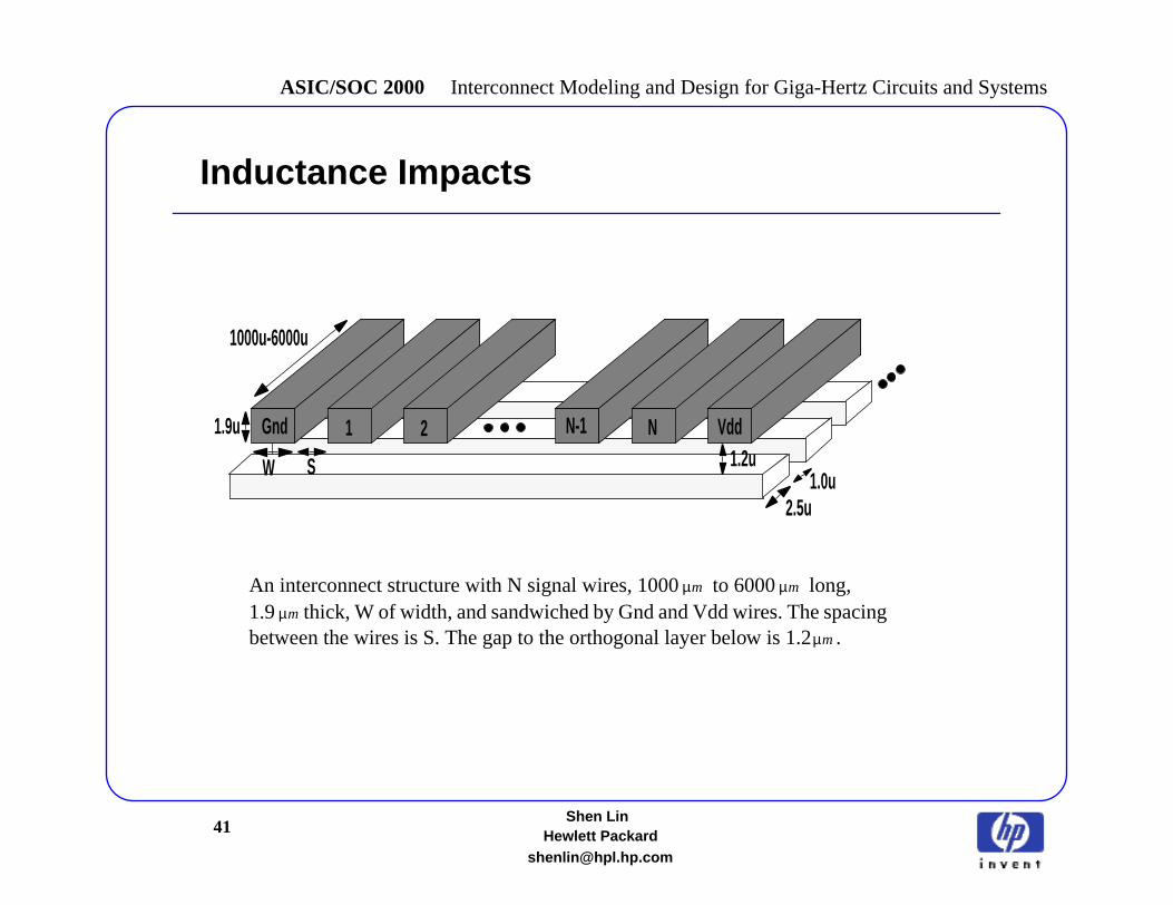
Inductance Impacts
1000u-6000u
Vdd1.9u1.2u
1.0u2.5u
N-1Gnd 1 2 N
W S
An interconnect structure with N signal wires, 1000 to 6000 long,1.9 thick, W of width, and sandwiched by Gnd and Vdd wires. The spacingbetween the wires is S. The gap to the orthogonal layer below is 1.2 .
µm µm
µm
µm
42Shen Lin
ASIC/SOC 2000 Interconnect Modeling and Design for Giga-Hertz Circuits and Systems
Hewlett [email protected]
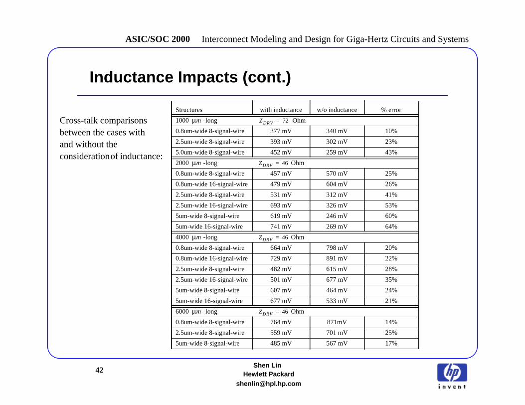
Inductance Impacts (cont.)
Structures with inductance w/o inductance % error
1000 -long Ohm
0.8um-wide 8-signal-wire 377 mV 340 mV 10%
2.5um-wide 8-signal-wire 393 mV 302 mV 23%
5.0um-wide 8-signal-wire 452 mV 259 mV 43%
2000 -long Ohm
0.8um-wide 8-signal-wire 457 mV 570 mV 25%
0.8um-wide 16-signal-wire 479 mV 604 mV 26%
2.5um-wide 8-signal-wire 531 mV 312 mV 41%
2.5um-wide 16-signal-wire 693 mV 326 mV 53%
5um-wide 8-signal-wire 619 mV 246 mV 60%
5um-wide 16-signal-wire 741 mV 269 mV 64%
4000 -long Ohm
0.8um-wide 8-signal-wire 664 mV 798 mV 20%
0.8um-wide 16-signal-wire 729 mV 891 mV 22%
2.5um-wide 8-signal-wire 482 mV 615 mV 28%
2.5um-wide 16-signal-wire 501 mV 677 mV 35%
5um-wide 8-signal-wire 607 mV 464 mV 24%
5um-wide 16-signal-wire 677 mV 533 mV 21%
6000 -long Ohm
0.8um-wide 8-signal-wire 764 mV 871mV 14%
2.5um-wide 8-signal-wire 559 mV 701 mV 25%
5um-wide 8-signal-wire 485 mV 567 mV 17%
µm ZDRV 72=
µm ZDRV 46=
µm ZDRV 46=
µm ZDRV 46=
Cross-talk comparisons
inductance:
between the cases withand without the
ofconsideration
43Shen Lin
ASIC/SOC 2000 Interconnect Modeling and Design for Giga-Hertz Circuits and Systems
Hewlett [email protected]
Inductance Impacts (cont.)
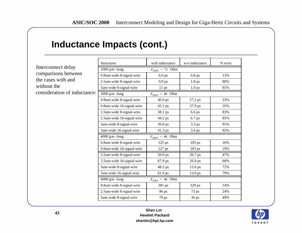
Structures with inductance w/o inductance % error
1000 -long Ohm
0.8um-wide 8-signal-wire 6.0 ps 6.8 ps 13%
2.5um-wide 8-signal-wire 9.0 ps 1.8 ps 80%
5um-wide 8-signal-wire 11 ps 1.0 ps 91%
2000 -long Ohm
0.8um-wide 8-signal-wire 40.6 ps 27.2 ps 33%
0.8um-wide 16-signal-wire 43.1 ps 27.9 ps 35%
2.5um-wide 8-signal-wire 38.1 ps 6.6 ps 83%
2.5um-wide 16-signal-wire 44.2 ps 6.7 ps 85%
5um-wide 8-signal-wire 36.8 ps 3.3 ps 91%
5um-wide 16-signal-wire 41.3 ps 3.4 ps 92%
4000 -long Ohm
0.8um-wide 8-signal-wire 125 ps 105 ps 16%
0.8um-wide 16-signal-wire 127 ps 103 ps 19%
2.5um-wide 8-signal-wire 50.0 ps 26.7 ps 47%
2.5um-wide 16-signal-wire 67.0 ps 26.9 ps 60%
5um-wide 8-signal-wire 48.5 ps 13.6 ps 72%
5um-wide 16-signal-wire 61.0 ps 13.0 ps 79%
6000 -long Ohm
0.8um-wide 8-signal-wire 381 ps 329 ps 14%
2.5um-wide 8-signal-wire 96 ps 73 ps 24%
5um-wide 8-signal-wire 70 ps 36 ps 49%
µm ZDRV 72=
µm ZDRV 46=
µm ZDRV 46=
µm ZDRV 46=
Interconnect delay
the cases with andwithout theconsideration of inductance:
comparisons between

44Shen Lin
ASIC/SOC 2000 Interconnect Modeling and Design for Giga-Hertz Circuits and Systems
Hewlett [email protected]
Summary of Inductance Impact Simulations
1. 0.8u-wide or narrower wires do not have significant inductance effects.
2. The worst case is all aggressors switch in the same direction
3. In general, with the inductance effects, signal rises faster but delay is longer.
The most serious inductance impact is the high-Q ringing, where
GG
aggressorsvictim
QL C⁄
Rs R+----------------≈ Overshoot
π–
4Q2
1–
-----------------------
exp=
4. The inductive crosstalk noise tops off at lengths of around 4000u to
6000u length.
The rise times shorter than one-half incur the worst ringing.2π LC
aggressors

45Shen Lin
ASIC/SOC 2000 Interconnect Modeling and Design for Giga-Hertz Circuits and Systems
Hewlett [email protected]
Purpose of Inductance Screen
Accurate and stable RLC delay and cross-talk estimations still
rely on computation-intensive simulations. Determining which nets
require the special consideration of inductance is important because
designers may apply those RC delay and cross-talk prediction methods,
proven to be fast and reliable, to as many nets as possible.
46Shen Lin
ASIC/SOC 2000 Interconnect Modeling and Design for Giga-Hertz Circuits and Systems
Hewlett [email protected]
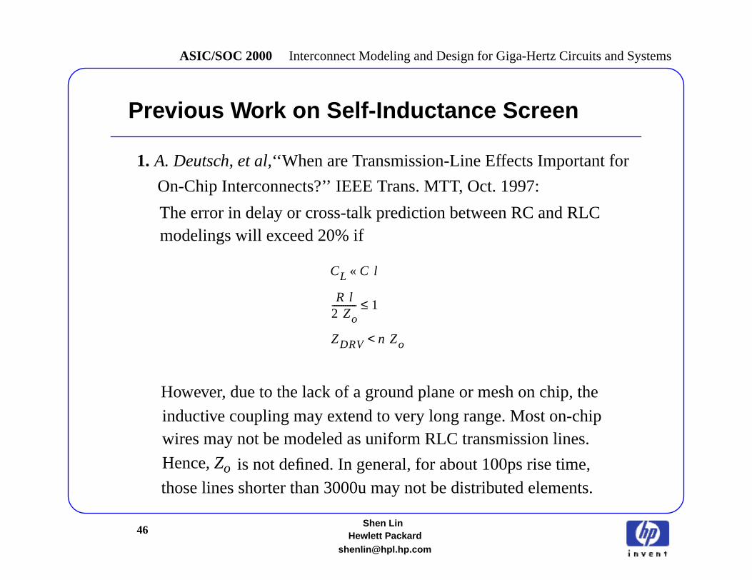
Previous Work on Self-Inductance Screen
1. A. Deutsch, et al,‘‘When are Transmission-Line Effects Important for
CL C l
R l2 Zo----------- 1
ZDRV n Zo<
≤
«
The error in delay or cross-talk prediction between RC and RLCmodelings will exceed 20% if
On-Chip Interconnects?’’ IEEE Trans. MTT, Oct. 1997:
However, due to the lack of a ground plane or mesh on chip, the
inductive coupling may extend to very long range. Most on-chipwires may not be modeled as uniform RLC transmission lines.
Hence, Zo is not defined. In general, for about 100ps rise time,those lines shorter than 3000u may not be distributed elements.
47Shen Lin
ASIC/SOC 2000 Interconnect Modeling and Design for Giga-Hertz Circuits and Systems
Hewlett [email protected]
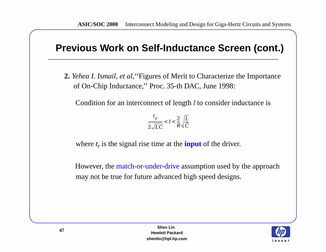
Previous Work on Self-Inductance Screen (cont.)
2. Yehea I. Ismail, et al,‘‘Figures of Merit to Characterize the Importance
tr
2 LC--------------- l
2R--- L
C----< <
Condition for an interconnect of lengthl to consider inductance is
However, thematch-or-under-drive assumption used by the approach
may not be true for future advanced high speed designs.
of On-Chip Inductance,’’ Proc. 35-th DAC, June 1998:
wheretr is the signal rise time at theinput of the driver.
48Shen Lin
ASIC/SOC 2000 Interconnect Modeling and Design for Giga-Hertz Circuits and Systems
Hewlett [email protected]
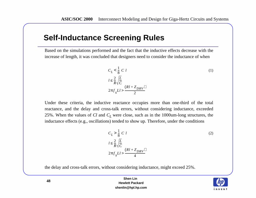
Self-Inductance Screening Rules
Based on the simulations performed and the fact that the inductive effects decrease with theincrease of length, it was concluded that designers need to consider the inductance of when
(1)
Under these criteria, the inductive reactance occupies more than one-third of the totalreactance, and the delay and cross-talk errors, without considering inductance, exceeded25%. When the values ofCl andCL were close, such as in the 1000um-long structures, theinductance effects (e.g., oscillations) tended to show up. Therefore, under the conditions
(2)
the delay and cross-talk errors, without considering inductance, might exceed 25%.
CL18--- C l
l2R--- L
C----
2π f sLlRl ZDRV+( )
2------------------------------->
≤
<
CL18--- C l
l2R--- L
C----
2π f sLlRl ZDRV+( )
4------------------------------->
≤
>

49Shen Lin
ASIC/SOC 2000 Interconnect Modeling and Design for Giga-Hertz Circuits and Systems
Hewlett [email protected]
S L6L1 L2 L3 L4 L5L1L2L3L4L5L6
L6 L5 L4 L3 L2 L1
1.9u thick Loop Ind. 2.21 n 2.06 n 1.88 n 1.65 n 1.31 n 0.689 n
1K-1G Hz % current 5.3% 5.6% 6.2% 7.0% 8.8% 17%
0.95u thick Loop Ind. 2.56 n 2.41 n 2.23 n 2.00 n 1.68 n 1.12 n
1 GHz % current 6.0% 6.4% 6.9% 7.7% 9.2% 13.8%
1.9u thick Loop Ind. 2.20 n 2.05 n 1.87 n 1.63 n 1.30 n 0.680 n
10 GHz % current 5.2% 5.6% 6.2% 7.1% 8.9% 17%
1.9u thick Loop Ind. 1.75 n 1.51 n 1.30 n 1.06 n 0.767 n 0.400 n
100 GHz % current 4.2% 4.9% 5.7% 7.0% 9.7% 18.5%
2000u
0.8u 0.8u
Distribution of High Frequency Return Currents
Mutual-Inductance Screening Rules
50Shen Lin
ASIC/SOC 2000 Interconnect Modeling and Design for Giga-Hertz Circuits and Systems
Hewlett [email protected]
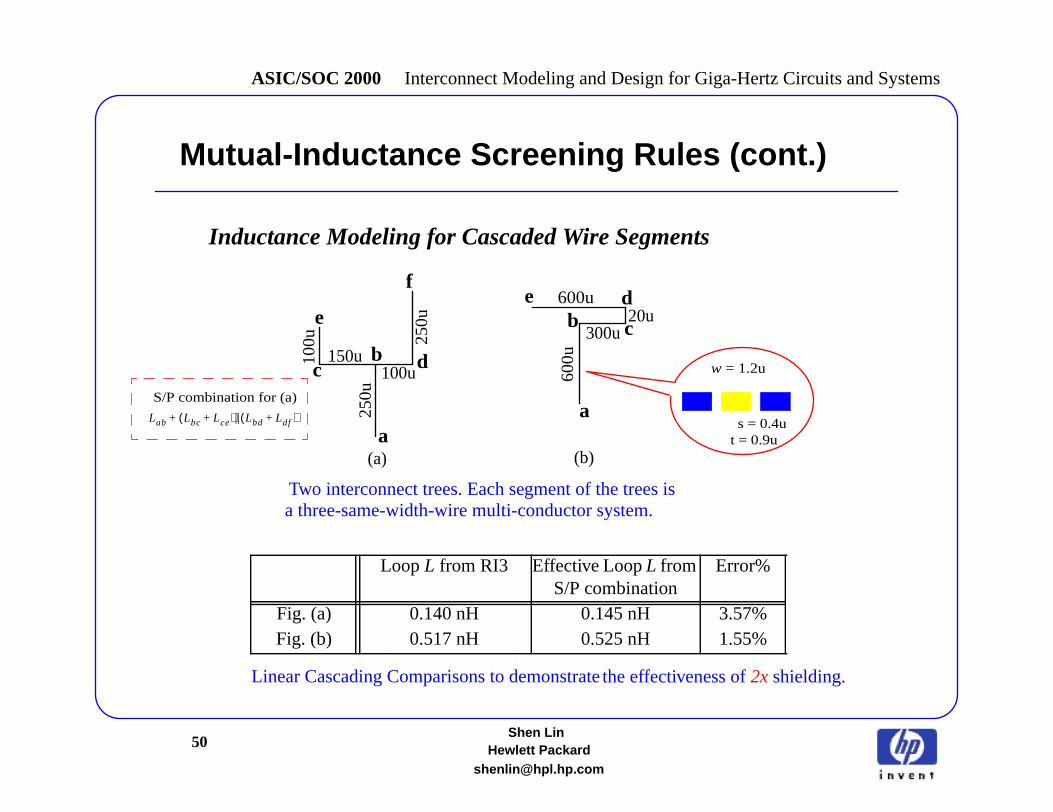
Mutual-Inductance Screening Rules (cont.)
a
d
a
bc d
e
f
25
0u
150u100u
600u
300u20u
w = 1.2u60
0u
b c
e
Two interconnect trees. Each segment of the trees isa three-same-width-wire multi-conductor system.
(a) (b)
25
0u
10
0u
s = 0.4u
LoopL from RI3 Effective LoopL fromS/P combination
Error%
Fig. (a) 0.140 nH 0.145 nH 3.57%Fig. (b) 0.517 nH 0.525 nH 1.55%
Linear Cascading Comparisons to demonstratethe effectiveness of2x shielding.
Inductance Modeling for Cascaded Wire Segments
Lab Lbc Lce+( )|| Lbd Ldf+( )+
t = 0.9u
S/P combination for (a)

51Shen Lin
ASIC/SOC 2000 Interconnect Modeling and Design for Giga-Hertz Circuits and Systems
Hewlett [email protected]
a2 a3 b0 b1 b2 b3 c0G V
1.9u
2000u
Drivers areBuf130 and receivers areBuf40 (CMOS 0.18u technology).
signal wires are2.5u wide with 1.25uspacing
Gnd/Vdd wirewidth
xtalk noiseat a3
b0-b3 switch up, c0 switches up 7.5u 0.73 mV
b0-b3 switch up, c0 quiet 7.5u 0.66 mV
b0-b3 switch up, e0 switches up 10.0u 0.48 mV
b0-b3 switch up; c0 quiet 10.0u 0.41 mV

52Shen Lin
ASIC/SOC 2000 Interconnect Modeling and Design for Giga-Hertz Circuits and Systems
Hewlett [email protected]
Mutual-Inductance Screening Rules (cont.)
1. In order to provide enough current return (shielding),
the width of the return path should be at least two
times the total width of all simultaneously switching
signals using that return path.
2. Quiet signal wire is as good as a ground wire of equal
width for high frequency current return (less than 5%
differences on delay and xtalk seen when the vdd wire
is replaced by a quiet signal wire in 0.8u case).
3. Low frequency currents may always find a ground wire
(or ground wires) for return.

53Shen Lin
ASIC/SOC 2000 Interconnect Modeling and Design for Giga-Hertz Circuits and Systems
Hewlett [email protected]
Efficient Inductance Modelings
1. The self-partially loop inductance for a trace on top of a ground
plane or in-between ground planes depends only on the trace’s
geometry (length, width, and thickness).
2. The mutual-partially loop inductance for two traces on top of a
ground plane or in-between ground planes depends only on their
geometry (lengths, widths, thicknesses, and spacing).
Partially-loop inductance is defined as the loop inductanceassuming that currents return only through the groundplane(s).
54Shen Lin
ASIC/SOC 2000 Interconnect Modeling and Design for Giga-Hertz Circuits and Systems
Hewlett [email protected]
Efficient Inductance Modelings (cont.)
Table-based Inductance Extraction:
1. Run RI3 or FastHenry to determine the self-inductances for
traces, microstrip- and strip-lines of several widths, lengths, and
2. Run RI3 or FastHenry to determine mutual-inductances for
two-line traces, microstrip- and strip-lines of several lengths,
widths, thicknesses, and spacings. Store the results in a table.
thicknesses. Store the results in a table.
3. To determine the inductances of an arbitrary trace, microstrip-
or strip-line, or of an arbitrary two-line traces, microstrip- or strip-
lines, use interpolations, such as cubic spline, from the inductances
of the closest line-structures predetermined in previous tables.
55Shen Lin
ASIC/SOC 2000 Interconnect Modeling and Design for Giga-Hertz Circuits and Systems
Hewlett [email protected]
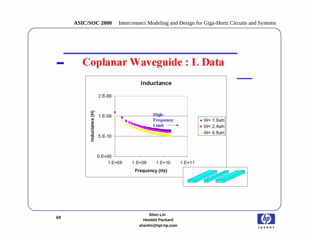
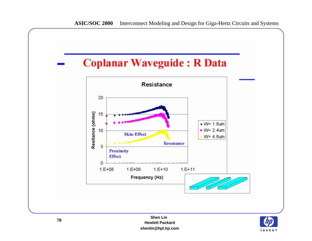
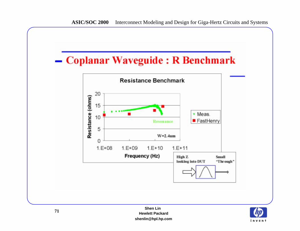
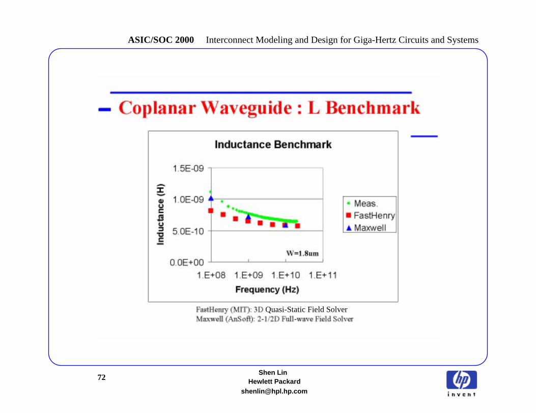
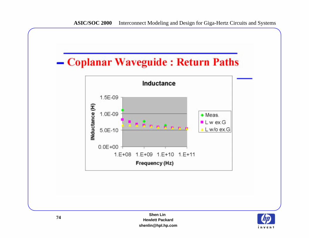
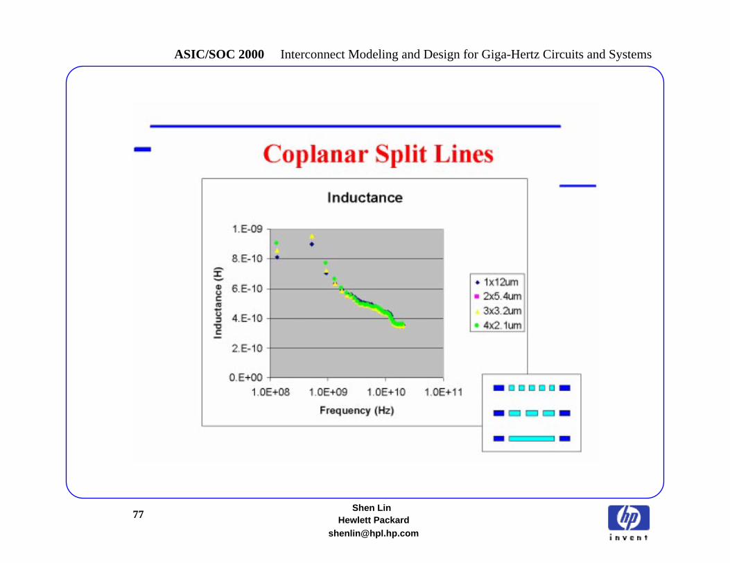
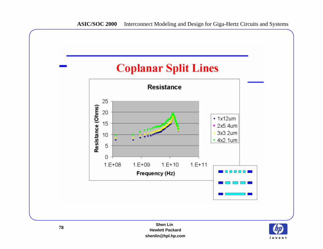
Inductance Test Chip Benchmark
Objective:
1. Extract frequency-dependent R, C, and L from test structures
2. Compare measurement and simulation
Previous Works:
1. IBM Research Report (1995), A. Deutsch, et. al., IBM
2. IITC Poster (1999), R. J. Friar, et. al., U. of Texas at Austin
3. IEDM Paper (1999), B. Keveland, et. al., Stanford U.

56Shen Lin
ASIC/SOC 2000 Interconnect Modeling and Design for Giga-Hertz Circuits and Systems
Hewlett [email protected]
57Shen Lin
ASIC/SOC 2000 Interconnect Modeling and Design for Giga-Hertz Circuits and Systems
Hewlett [email protected]
58Shen Lin
ASIC/SOC 2000 Interconnect Modeling and Design for Giga-Hertz Circuits and Systems
Hewlett [email protected]
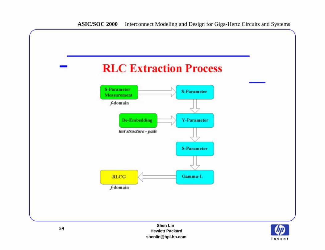
59Shen Lin
ASIC/SOC 2000 Interconnect Modeling and Design for Giga-Hertz Circuits and Systems
Hewlett [email protected]
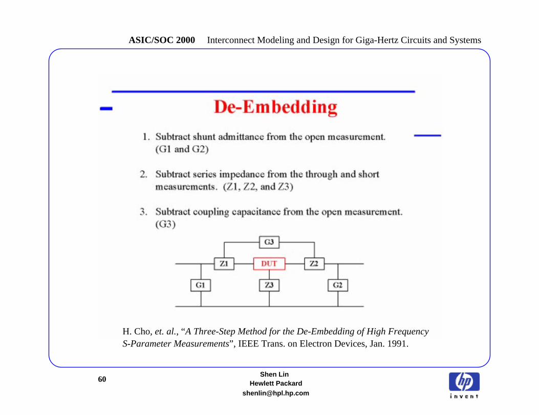
60Shen Lin
ASIC/SOC 2000 Interconnect Modeling and Design for Giga-Hertz Circuits and Systems
Hewlett [email protected]
H. Cho, et. al., “A Three-Step Method for the De-Embedding of High FrequencyS-Parameter Measurements”, IEEE Trans. on Electron Devices, Jan. 1991.
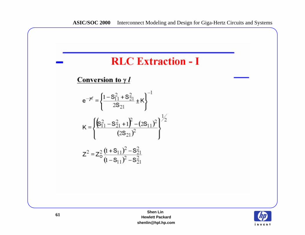
61Shen Lin
ASIC/SOC 2000 Interconnect Modeling and Design for Giga-Hertz Circuits and Systems
Hewlett [email protected]
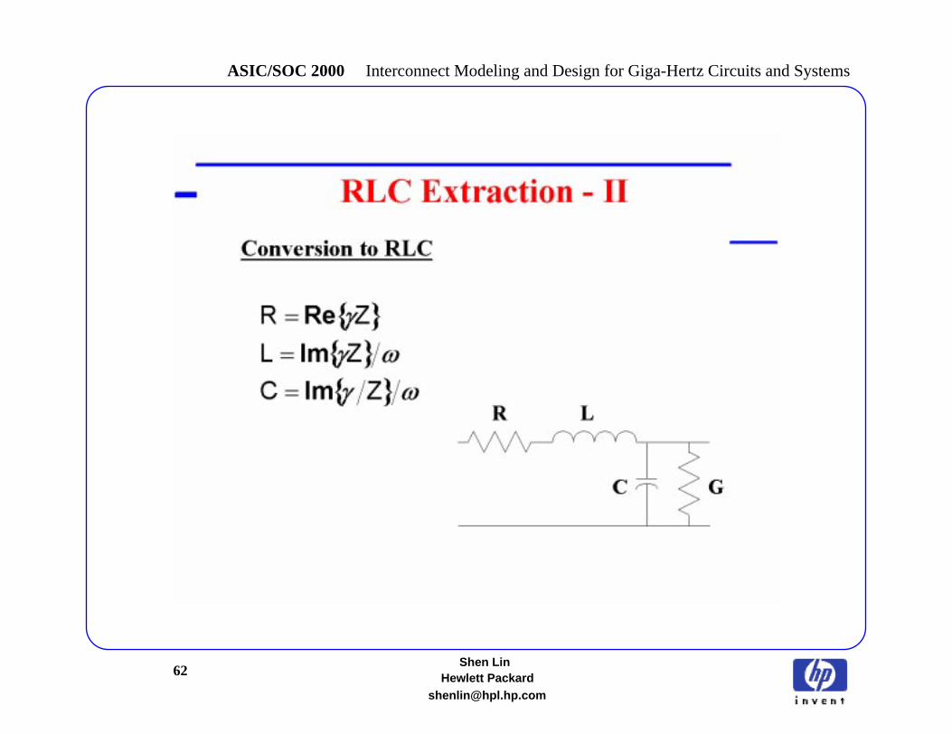
62Shen Lin
ASIC/SOC 2000 Interconnect Modeling and Design for Giga-Hertz Circuits and Systems
Hewlett [email protected]

63Shen Lin
ASIC/SOC 2000 Interconnect Modeling and Design for Giga-Hertz Circuits and Systems
Hewlett [email protected]
64Shen Lin
ASIC/SOC 2000 Interconnect Modeling and Design for Giga-Hertz Circuits and Systems
Hewlett [email protected]

65Shen Lin
ASIC/SOC 2000 Interconnect Modeling and Design for Giga-Hertz Circuits and Systems
Hewlett [email protected]
66Shen Lin
ASIC/SOC 2000 Interconnect Modeling and Design for Giga-Hertz Circuits and Systems
Hewlett [email protected]
67Shen Lin
ASIC/SOC 2000 Interconnect Modeling and Design for Giga-Hertz Circuits and Systems
Hewlett [email protected]
68Shen Lin
ASIC/SOC 2000 Interconnect Modeling and Design for Giga-Hertz Circuits and Systems
Hewlett [email protected]
69Shen Lin
ASIC/SOC 2000 Interconnect Modeling and Design for Giga-Hertz Circuits and Systems
Hewlett [email protected]
70Shen Lin
ASIC/SOC 2000 Interconnect Modeling and Design for Giga-Hertz Circuits and Systems
Hewlett [email protected]
71Shen Lin
ASIC/SOC 2000 Interconnect Modeling and Design for Giga-Hertz Circuits and Systems
Hewlett [email protected]
72Shen Lin
ASIC/SOC 2000 Interconnect Modeling and Design for Giga-Hertz Circuits and Systems
Hewlett [email protected]
Quasi-Static Field Solver

73Shen Lin
ASIC/SOC 2000 Interconnect Modeling and Design for Giga-Hertz Circuits and Systems
Hewlett [email protected]
74Shen Lin
ASIC/SOC 2000 Interconnect Modeling and Design for Giga-Hertz Circuits and Systems
Hewlett [email protected]

75Shen Lin
ASIC/SOC 2000 Interconnect Modeling and Design for Giga-Hertz Circuits and Systems
Hewlett [email protected]

76Shen Lin
ASIC/SOC 2000 Interconnect Modeling and Design for Giga-Hertz Circuits and Systems
Hewlett [email protected]
77Shen Lin
ASIC/SOC 2000 Interconnect Modeling and Design for Giga-Hertz Circuits and Systems
Hewlett [email protected]
78Shen Lin
ASIC/SOC 2000 Interconnect Modeling and Design for Giga-Hertz Circuits and Systems
Hewlett [email protected]

79Shen Lin
ASIC/SOC 2000 Interconnect Modeling and Design for Giga-Hertz Circuits and Systems
Hewlett [email protected]
Quasi-Static Field Solver
80Shen Lin
ASIC/SOC 2000 Interconnect Modeling and Design for Giga-Hertz Circuits and Systems
Hewlett [email protected]
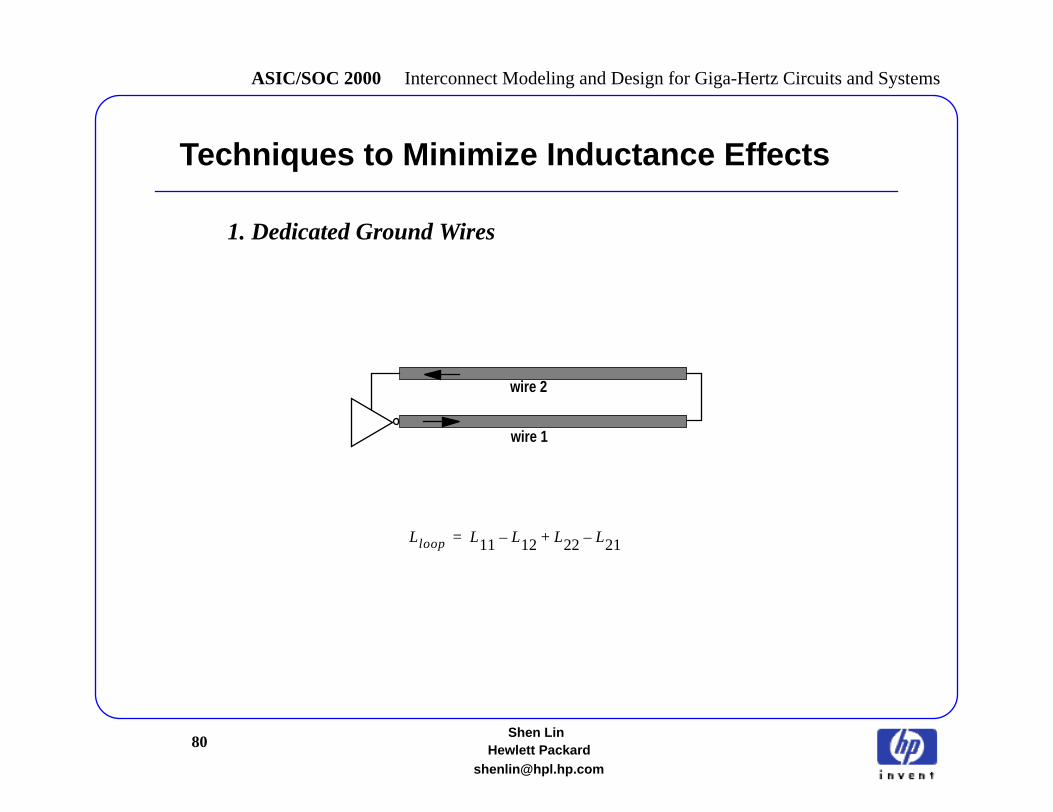
Techniques to Minimize Inductance Effects
1. Dedicated Ground Wires
wire 1
wire 2
Lloop L11 L12– L22 L21–+=
81Shen Lin
ASIC/SOC 2000 Interconnect Modeling and Design for Giga-Hertz Circuits and Systems
Hewlett [email protected]
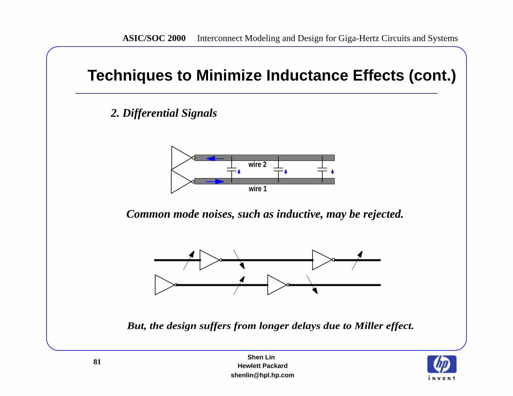
Techniques to Minimize Inductance Effects (cont.)
2. Differential Signals
wire 1
wire 2
But, the design suffers from longer delays due to Miller effect.
Common mode noises, such as inductive, may be rejected.
82Shen Lin
ASIC/SOC 2000 Interconnect Modeling and Design for Giga-Hertz Circuits and Systems
Hewlett [email protected]
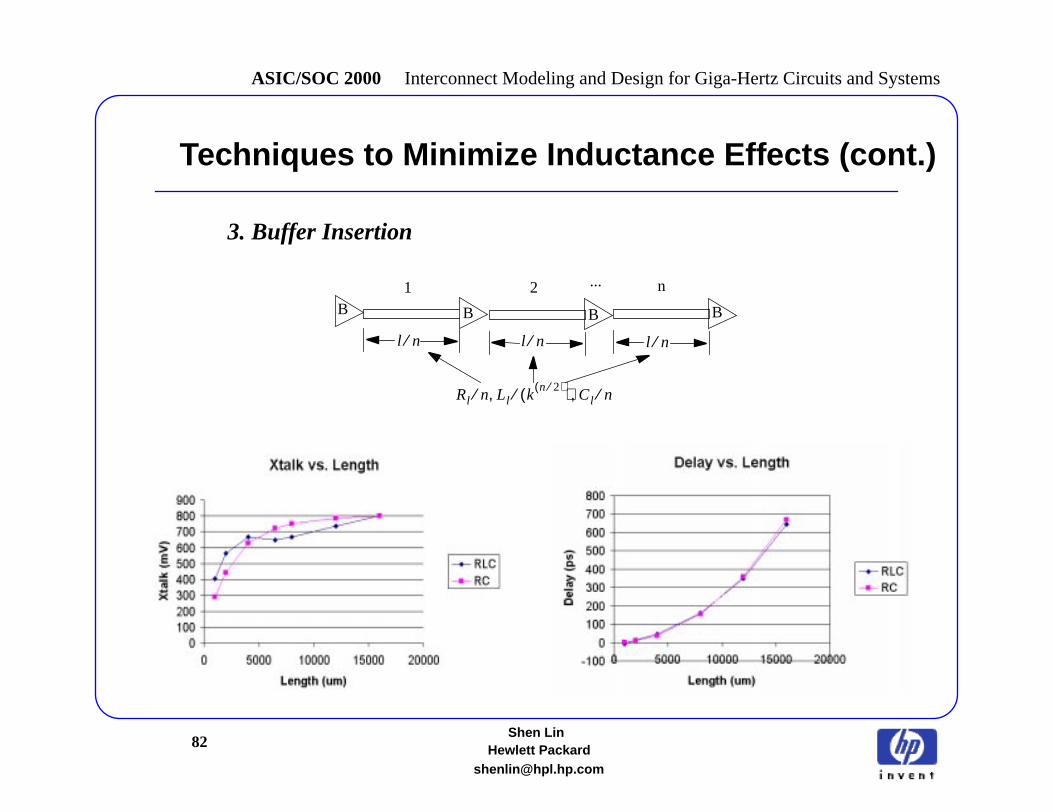
Techniques to Minimize Inductance Effects (cont.)
3. Buffer Insertion
B B B B
Rl n⁄ Ll kn 2⁄( )( )⁄ Cl n⁄, ,
1 2 ... n
l n⁄ l n⁄ l n⁄
83Shen Lin
ASIC/SOC 2000 Interconnect Modeling and Design for Giga-Hertz Circuits and Systems
Hewlett [email protected]
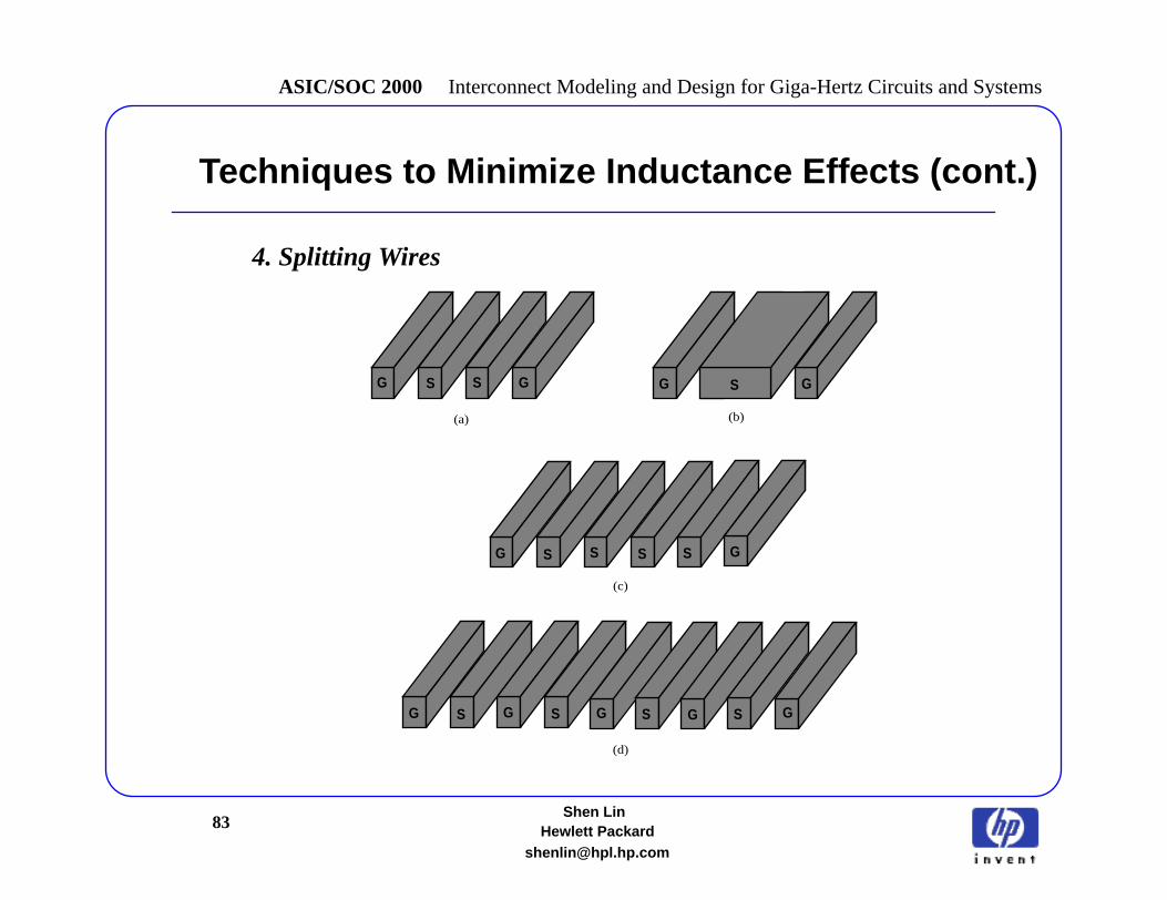
Techniques to Minimize Inductance Effects (cont.)
4. Splitting Wires
G S S G G G
(a) (b)
G S SS S
(c)
G G SS G
(d)
G
G GSS
S
84Shen Lin
ASIC/SOC 2000 Interconnect Modeling and Design for Giga-Hertz Circuits and Systems
Hewlett [email protected]
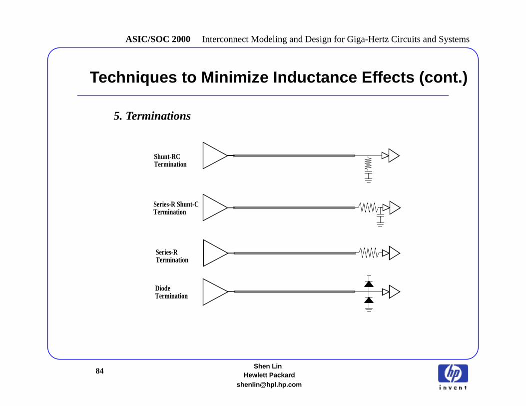
Techniques to Minimize Inductance Effects (cont.)
5. Terminations
Series-R
Series-R Shunt-C
Shunt-RC
DiodeTermination
Termination
Termination
Termination
85Shen Lin
ASIC/SOC 2000 Interconnect Modeling and Design for Giga-Hertz Circuits and Systems
Hewlett [email protected]
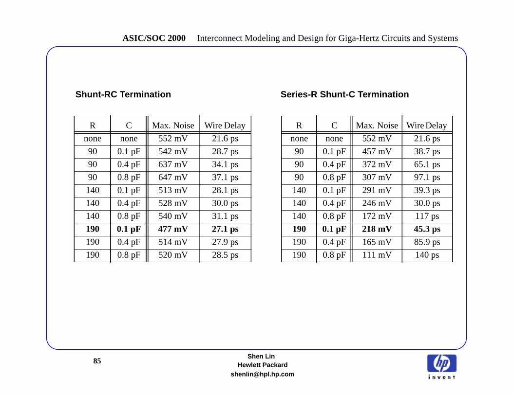
R C Max. Noise Wire Delay
none none 552 mV 21.6 ps
90 0.1 pF 542 mV 28.7 ps
90 0.4 pF 637 mV 34.1 ps
90 0.8 pF 647 mV 37.1 ps
140 0.1 pF 513 mV 28.1 ps
140 0.4 pF 528 mV 30.0 ps
140 0.8 pF 540 mV 31.1 ps
190 0.1 pF 477 mV 27.1 ps190 0.4 pF 514 mV 27.9 ps
190 0.8 pF 520 mV 28.5 ps
R C Max. Noise Wire Delay
none none 552 mV 21.6 ps
90 0.1 pF 457 mV 38.7 ps
90 0.4 pF 372 mV 65.1 ps
90 0.8 pF 307 mV 97.1 ps
140 0.1 pF 291 mV 39.3 ps
140 0.4 pF 246 mV 30.0 ps
140 0.8 pF 172 mV 117 ps
190 0.1 pF 218 mV 45.3 ps190 0.4 pF 165 mV 85.9 ps
190 0.8 pF 111 mV 140 ps
Series-R Shunt-C TerminationShunt-RC Termination
86Shen Lin
ASIC/SOC 2000 Interconnect Modeling and Design for Giga-Hertz Circuits and Systems
Hewlett [email protected]
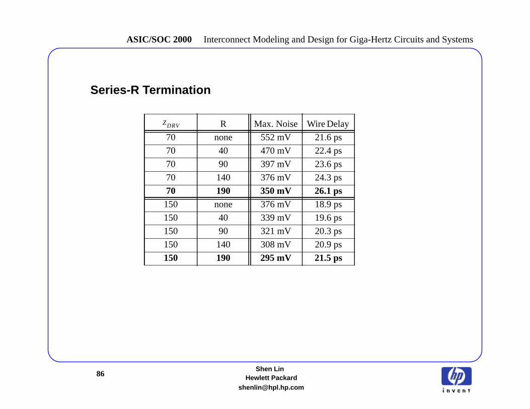
R Max. Noise Wire Delay
70 none 552 mV 21.6 ps
70 40 470 mV 22.4 ps
70 90 397 mV 23.6 ps
70 140 376 mV 24.3 ps
70 190 350 mV 26.1 ps150 none 376 mV 18.9 ps
150 40 339 mV 19.6 ps
150 90 321 mV 20.3 ps
150 140 308 mV 20.9 ps
150 190 295 mV 21.5 ps
ZDRV
Series-R Termination
87Shen Lin
ASIC/SOC 2000 Interconnect Modeling and Design for Giga-Hertz Circuits and Systems
Hewlett [email protected]
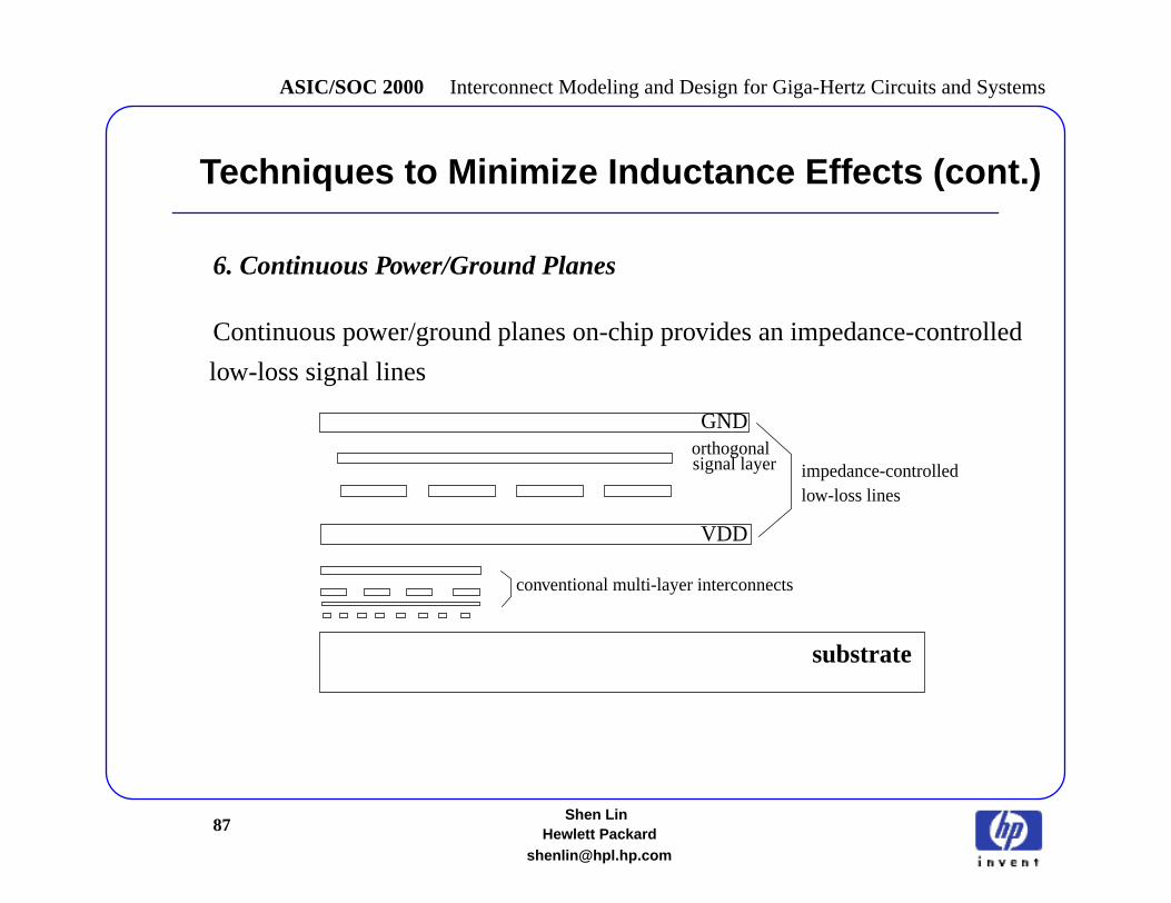
Techniques to Minimize Inductance Effects (cont.)
6. Continuous Power/Ground Planes
conventional multi-layer interconnects
impedance-controlledlow-loss lines
GND
VDD
substrate
orthogonalsignal layer
Continuous power/ground planes on-chip provides an impedance-controlled
low-loss signal lines
88Shen Lin
ASIC/SOC 2000 Interconnect Modeling and Design for Giga-Hertz Circuits and Systems
Hewlett [email protected]
Summary
We discussed
The on-chip inductance is not scalable and non-orthogonal wires are
may not be treated as transmission lines.
be preferred and let the circuit simulator determine the return path.
3. the skin effect and the proximity effect.
interconnect structures, which are mainly caused by over-drive and low
coupling noise and oscillation caused by over-shoot may be effectively
1. the difference between on-chip inductance and off-chip consideration.
5. several important design solutions to cope with inductance effects.6. based on the correct understanding of on-chip inductance, the inductive
controlled in the future’s multi-GHz chips.
4. the inductance impact on delay and cross-talk noise for several
resistance. The simulation results lead to the answer of the question “whendo we need to consider inductance”.
2. how to calculate inductance. We mention that partial inductance should
almost all inductively coupled. Therefore, the on-chip interconnects

89Shen Lin
ASIC/SOC 2000 Interconnect Modeling and Design for Giga-Hertz Circuits and Systems
Hewlett [email protected]
Bibliography
[1] CK Cheng, John Lillis, Shen Lin, and Norman Chang, “InterconnectAnalysis and Synthesis,” John Wiley & Sons, Inc., 1999.
[2] Frederick W. Grover, “Inductance Calculations Working Formulasand Tables,” Dover Publications, 1946.
[3] Al Ruehli, “Inductance Calculations in a Complex IntegratedCircuit Environment,” IBM J. Research and Development, Sep. 1972.
[4] A. Deutsch, H. Smith, et al, ‘‘When are Transmission-Line EffectsImportant for On-Chip Interconnects?’’ IEEE Trans. Microwave TheoryTech., vol. 45, pp. 1836-1846, Oct. 1997.
[5] Yehea I. Ismail, Eby G. Friedman, and Jose L. Neves,‘‘Figures of Merit toCharacterize the Importance of On-Chip Inductance,’’ Proc. 35-th DesignAutomation Conference, pp. 560-565, San Francisco, Jun. 1998.
[6] N. Chang, S. Lin, L. He, S. Nakagawa, and W. Xie, “Clocktree RLCExtraction with Efficient Inductance Modeling,” to appear DATE2000.
90Shen Lin
ASIC/SOC 2000 Interconnect Modeling and Design for Giga-Hertz Circuits and Systems
Hewlett [email protected]
Acknowledgement
N. Chang, S. Nakagawa, S. Naffzinger, D. Krueger,
HP
T. Michalka, A. Meyer, W. Xie, and K. Lee
Richard Chang
Stanford University
Lei He
University of Wisconsin