Embed Size (px)
Citation preview
1
Effects of High Switching Frequency on Buck Regulators

2
AbstractThe switching frequency is an operating parameter which affects nearly every performance characteristic of the supply, as well as the cost. Determining the proper switching frequency for a particular design requires that the designer knows the application sensitivity to each of these characteristics, in order to simultaneously minimize cost and satisfy all application requirements.
This presentation presents the effects of switching frequency on buck switching regulator operating characteristics, and how switchingfrequency affects the cost of the supply.

3
Benefits of High Switching Frequency1. Smaller converter
Smaller can be cheaper – up to a certain power outputBeyond that power level small size might be worth some added cost
2. Transient response can improve with higher switching frequency.
3. Avoids frequency bands in which noise would be disruptiveAM BroadcastVehicle motion/position monitors
Drawbacks of High Switching FrequencyEfficiency is worse
Switching loss is proportional to switching frequencyFET Switch drive power is also proportional to frequency, and isusually provided by a Linear Regulator!
Maximum conversion ratio (maximum VIN) is lowerDropout voltage (minimum VIN) is higherCurrent limit accuracy is likely to be worse
4
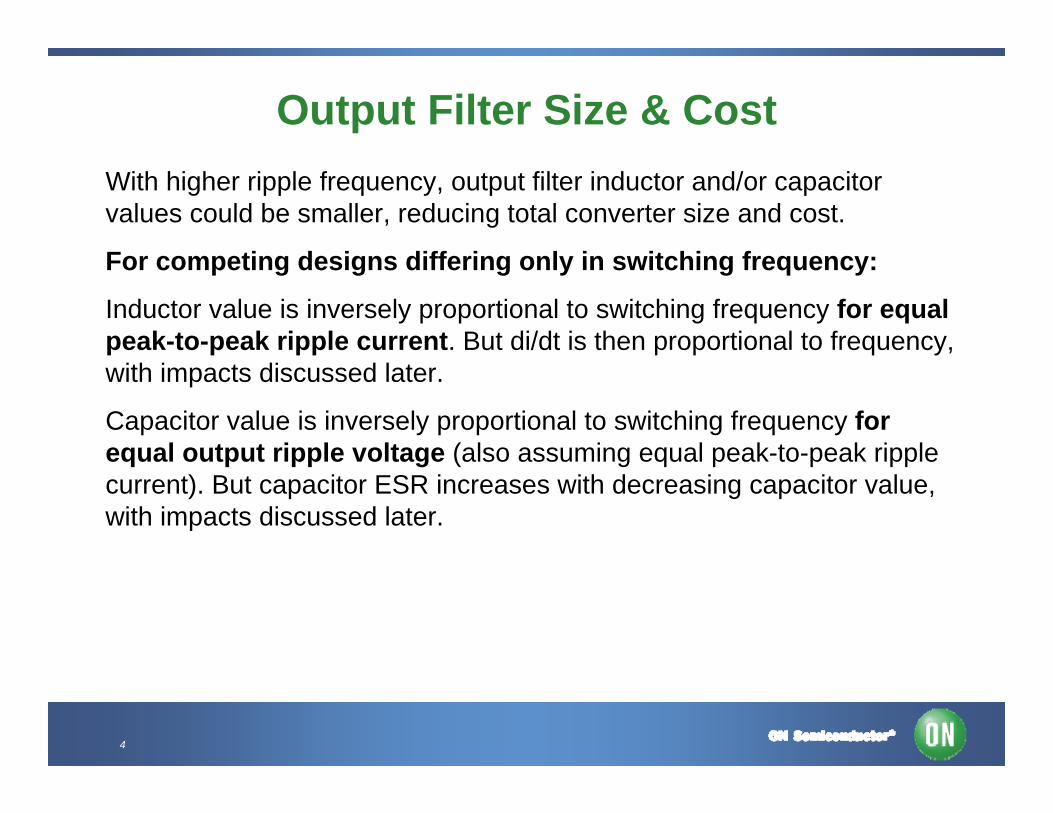
Output Filter Size & CostWith higher ripple frequency, output filter inductor and/or capacitor values could be smaller, reducing total converter size and cost.
For competing designs differing only in switching frequency:
Inductor value is inversely proportional to switching frequency for equal peak-to-peak ripple current. But di/dt is then proportional to frequency, with impacts discussed later.
Capacitor value is inversely proportional to switching frequency for equal output ripple voltage (also assuming equal peak-to-peak ripple current). But capacitor ESR increases with decreasing capacitor value, with impacts discussed later.

5
Inductor Size or Dissipation Reduction?The lower inductor value permitted by higher frequency has lower I2R loss for the same core since the number of turns decreased. But if thinner wire is also used, such that the DC resistance is not changed, using a core with a shorter mean magnetic path will result in a smaller volume inductor, with less core material experiencing the same loss per unit volume.
Example (Wurth WE-PD series)Induct Induct Isat Volume Volume DCR Freq Freq(μH) Ratio (A) (mm2) Ratio (mΩ) (kHz) Ratio4.7 1.00 3.9A 170.5 1.00 35 2000 5.00 S-type22 4.68 3.8A 864 5.07 36 400 1.00 L-type
Powdered iron core loss is significant, and is proportional to frequency for the same peak flux level (same % saturation), so the above examples would have identical I2R and core losses, with inductor volume inversely proportional to frequency.So inductor loss can be traded off for inductor volume, but the product of loss and volume reductions cannot exceed the frequency increase factor.

6
Capacitor Size Reduction – Value ImpactThe smaller capacitor value permitted by higher switching frequency increases the converter high frequency output impedance.
Output Impedance vs Frequency
Frequency
Low C
Hi C
Higher Impedance
Low CESR
Hi CESR
ZcHi CZc
ESL
Low C
ESL
7
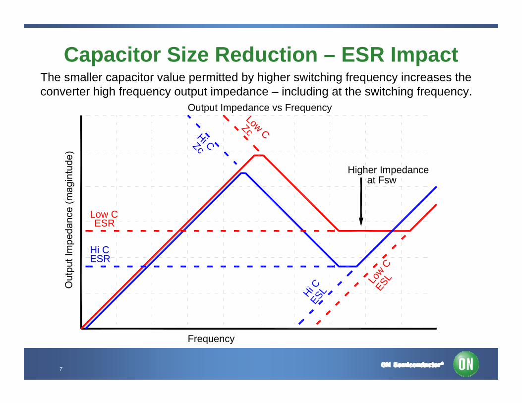
Capacitor Size Reduction – ESR ImpactThe smaller capacitor value permitted by higher switching frequency increases the converter high frequency output impedance – including at the switching frequency.
Output Impedance vs Frequency
Frequency
Low C
Hi C
Higher Impedance
Low CESR
Hi CESR
ZcHi CZc
ESL
Low C
ESL
at Fsw
8
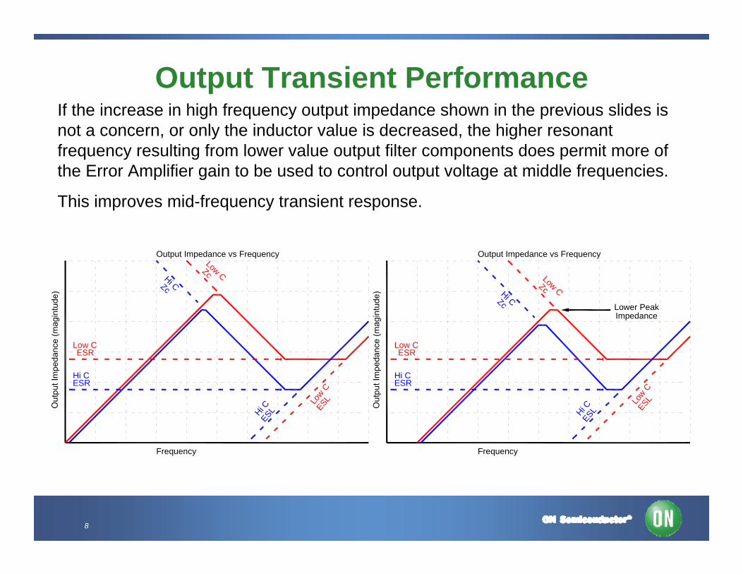
Output Transient PerformanceIf the increase in high frequency output impedance shown in the previous slides is not a concern, or only the inductor value is decreased, the higher resonant frequency resulting from lower value output filter components does permit more of the Error Amplifier gain to be used to control output voltage at middle frequencies.
This improves mid-frequency transient response.
Output Impedance vs Frequency
Frequency
Low C
Hi C
Lower Peak
Low CESR
Hi CESR
ZcHi CZc
ESL
Low C
ESL
Impedance
Output Impedance vs Frequency
Frequency
Low C
Hi C
Low CESR
Hi CESR
ZcHi CZc
ESL
Low C
ESL

9
Capacitor Size Reduction – ESR Impact
The smaller capacitor value permitted by higher switching frequency will typically have proportionally higher ESR for equally smaller case volume. But the relationship of ESR to case volume is highly variable, so must be carefully examined for the particular application.
Assuming an inversely proportional scaling of ESR with case volume, reaping the volume reduction afforded by higher switching frequency affects the output ripple voltage of the converter.

10
Component Volume
5:1 frequency ratio assumed for this graph.Linear Regulator component volume reflects case size needed for cooling.
0 1 2 3 4 5 6 7 9 108Maximum Converter Power Output
Com
pone
nt V
olum
e
Linea
r Reg
ulator
External Freewheeling Diode
Monolithic
2 External
Standard Frequency
High Frequency Switching Regulator
External Freewheeling Diode
Monolithic
Switches
Switching Regulator
11
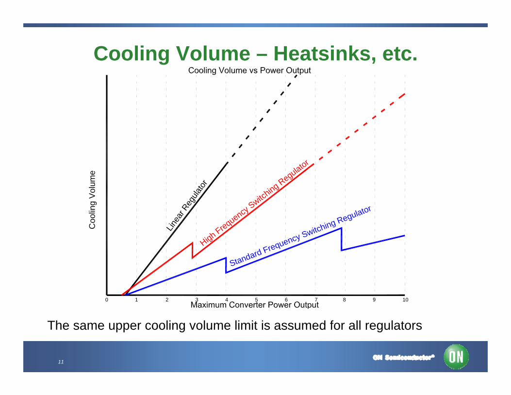
Cooling Volume – Heatsinks, etc.
The same upper cooling volume limit is assumed for all regulators
0 1 2 3 4 5 6 7 9 108
Coo
ling
Vol
ume
Linea
r Reg
ulator
Standard Frequency Switching Regulator
High Frequency Switch
ing Regulator

12
How Frequency Affects Total Converter Size
Sum of previous 2 graphs
0 1 2 3 4 5 6 7 9 108Maximum Converter Power Output
Tota
l Con
verte
r Vol
ume
High Frequency Switching Regulator
Standard Frequency
Switching Regulator
Linea
r Reg
ulator

13
Efficiency
Switching loss increases with increasing switching frequency due to the greater number or constant energy switching events per time.Besides this, if switching frequency is sufficiently high, Synchronous Rectification cannot be implemented – further increasing conduction loss for high conversion ratio applications.Gate drive current also hurts efficiency – especially at high battery – unless bootstrapped from the output.
14
Regulator Characteristics Determine Impacts
The impacts of high frequency switching depend on the answers to several questions:
1. Is the regulator using Voltage-mode or Current-mode to control output voltage?
Conversion ratio is limited for Current-mode control
2. Does the application need the efficiency of Synchronous Rectification?
If yes, then switching frequency or input voltage range will be restricted.
3. Is the regulator in Continuous Conduction mode (CCM) or Discontinuous Conduction mode (DCM)?
With DCM, light load switching frequency will decrease.

15
Reduced Conversion Ratio (lower max VIN)
Max Switching Frequency versus Input Voltage
0200400600800
1000120014001600180020002200240026002800300032003400
2 4 6 8 10 12 14 16 18 20 22 24 26 28 30 32 34 36 38 40 42 44 46 48 50Input Voltage (V)
Max
Sw
itchi
ng F
requ
ency
(kH
z)
Vout=0.5Vout=1.0Vout=1.5Vout=2.0Vout=2.5Vout=3.0Vout=3.5Vout=4.0Vout=4.5Vout=5.0
Current-mode converters typically have a blanking time, which sets the minimum D for a given Vout, and therefore max VIN, that will be regulated without reducing switching frequency (pulse skipping).
Graphs reflect 70ns blanking time.
Vout versus Input Voltage
0
1
2
3
4
5
6
2 4 6 8 10 12 14 16 18 20 22 24 26 28 30 32 34 36 38 40 42
Input Voltage (V)V
out (
V)
Min Vout@1800kHzMin Vout@2100kHzMin Vout@2400kHz

16
Reduced Conversion Ratio (lower max VIN)
As the load on a non-synchronous, current-mode buck converter approaches zero, the switching frequency will decrease in an irregular manner (pulse skipping) since a VIN-dependent charge must be delivered to the output during the blanking time at each turnon. For a given load current, FSWAVERAGE = Load current/(VIN – Vout)
Why be concerned with performance at loads <10% of max converter rating?Loads will be in sleep mode some of the time Bench evaluation should not exhibit pulse skipping over a wide load range
Even for output voltages that do not produce pulse skipping at high VIN, dissipation caused by Gate Drive current is high if the current is derived directly from VIN. Bootstrapping from the output can sometimes be used to avoid this excessive dissipation.
17
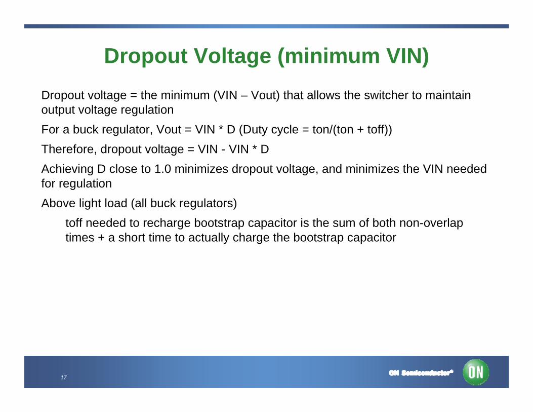
Dropout Voltage (minimum VIN)Dropout voltage = the minimum (VIN – Vout) that allows the switcher to maintain output voltage regulationFor a buck regulator, Vout = VIN * D (Duty cycle = ton/(ton + toff))Therefore, dropout voltage = VIN - VIN * DAchieving D close to 1.0 minimizes dropout voltage, and minimizes the VIN needed for regulationAbove light load (all buck regulators)
toff needed to recharge bootstrap capacitor is the sum of both non-overlap times + a short time to actually charge the bootstrap capacitor
18
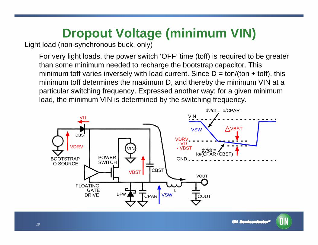
Dropout Voltage (minimum VIN)Light load (non-synchronous buck, only)
For very light loads, the power switch ‘OFF’ time (toff) is required to be greater than some minimum needed to recharge the bootstrap capacitor. This minimum toff varies inversely with load current. Since D = ton/(ton + toff), this minimum toff determines the maximum D, and thereby the minimum VIN at a particular switching frequency. Expressed another way: for a given minimum load, the minimum VIN is determined by the switching frequency.
DRIVEGATE
COUTDFW
CBSTVOUT
BOOTSTRAP POWER
L
DBST
SWITCH
VIN
Q SOURCE
FLOATING
GND
VIN
VDRVVDRV
- VD
VD
VBST
VBSTVSW
VSW
- VBST
CPAR
dv/dt = Io/CPAR
dv/dt =Io/(CPAR+CBST)
19
Looser Current LimitLower inductor values increase the current limit variation due to the current sense
delay. This is because V = L di/dt, or di = (VIN-VOUT)/L x dt:1. The bandwidth of current monitoring circuitry causes delay
Delay is highly dependent upon overdrive, and consequently nearly independent on VIN (higher di/dt is compensated by shorter delay)
2. Noise blanking time following switch turnon determines the shutoff delay during a dead short. The peak current limit is then proportional to di/dt.VIN variation causes di/dt variation, causing average current to varyVout droops when in current limit, increasing di/dt & raising average
current
20
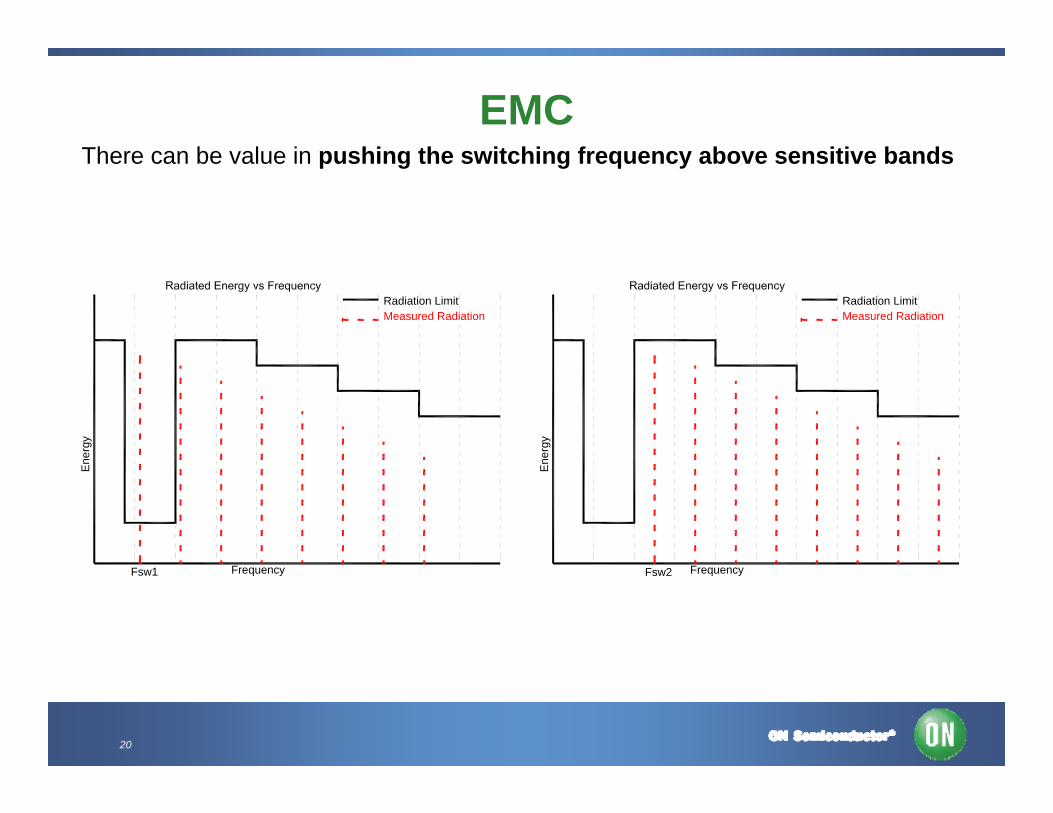
EMCThere can be value in pushing the switching frequency above sensitive bands
Frequency
Ener
gy
Radiation LimitMeasured Radiation
Fsw1 Frequency
Ener
gy
Radiation LimitMeasured Radiation
Fsw2
21
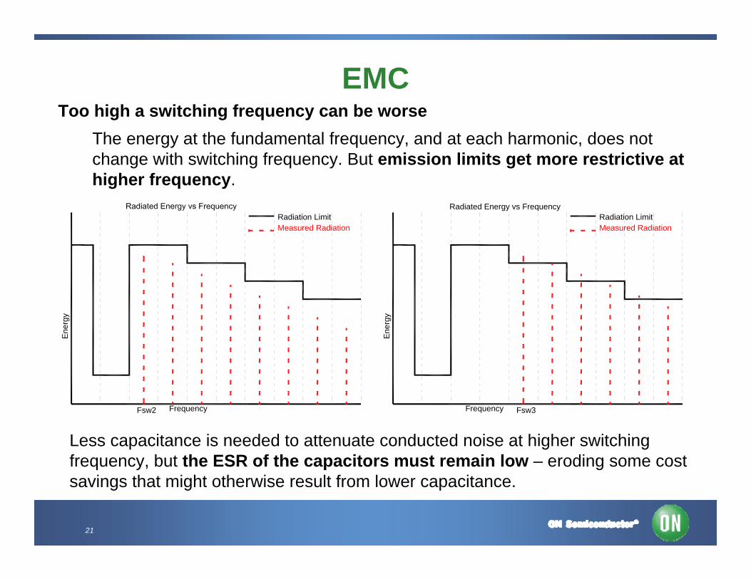
EMCToo high a switching frequency can be worse
The energy at the fundamental frequency, and at each harmonic, does not change with switching frequency. But emission limits get more restrictive at higher frequency.
Frequency
Ener
gy
Radiation LimitMeasured Radiation
Fsw2 Frequency
Ener
gy
Radiation LimitMeasured Radiation
Fsw3
Radiated Energy vs Frequency
Less capacitance is needed to attenuate conducted noise at higher switching frequency, but the ESR of the capacitors must remain low – eroding some cost savings that might otherwise result from lower capacitance.
22
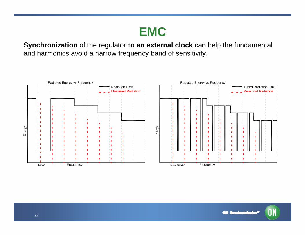
EMCSynchronization of the regulator to an external clock can help the fundamental and harmonics avoid a narrow frequency band of sensitivity.
Frequency
Ener
gy
Radiation LimitMeasured Radiation
Fsw1 Frequency
Ener
gy
Tuned Radiation LimitMeasured Radiation
Fsw tuned

23
References
ON Semiconductor Switchmode Power Supply Reference Manual Rev 2 Apr-2000
Unitrode Application note U-68A

24
For More Information
• View the extensive portfolio of power management products from ON Semiconductor at www.onsemi.com
• View reference designs, design notes, and other material supporting automotive applications at www.onsemi.com/automotive