Embed Size (px)
Citation preview
Application ReportSLVA630A–January 2014–Revised October 2014
Output Ripple Voltage for Buck Switching Regulator
Surinder P. Singh, Ph.D., Manager, Power Applications Group............................. WEBENCH® Design Center
ABSTRACTSwitched-mode power supplies (SMPSs) are used to regulate voltage to a certain level. SMPSs have aninherent switching action, which causes the currents and voltages in the circuit to switch and fluctuate.The output voltage also has ripple on top of the regulated steady-state DC value. Designers of powersystems consider the output voltage ripple to be both a key parameter for design considerations and a keyfigure of merit. The online WEBENCH® Power Designer recognizes the key importance of peak-to-peakvoltage output ripple voltage—the ripple voltage is calculated and reported in the visualizer [1]. Thisapplication report presents a closed-form analytical formulation for the output voltage ripple waveform andthe peak-to-peak ripple voltage. This formulation is accurate over all regions of operation and harmonizesthe peak-to-peak ripple voltage calculation over all regions of operation. The new analytical formulationpresented in this application report gives an accurate evaluation of the output ripple as compared to thesimplified linear or root-mean square (RMS) approximations often used.
In this application report, the analytical model for output voltage waveform and peak-to-peak ripple voltagefor buck is derived. This model is validated against SPICE TINA-TI simulations. This report presents thebehavior of ripple peak-to-voltage for various input conditions and choices of output capacitor andcompare it against SPICE TINA-TI results. This report analyzes and presents the validity of the linear andthe RMS approximation. Examples from the TI portfolio are presented that compare the experimentalripple waveforms in different regimes.
Contents1 Introduction ................................................................................................................... 22 Output Voltage Ripple Waveform Derivation............................................................................. 33 Output Peak-to-Peak Ripple Voltage...................................................................................... 54 Validation Against SPICE................................................................................................... 75 Results ........................................................................................................................ 86 Approximations ............................................................................................................. 107 Examples from TI Devices and Evaluation Modules (EVMs)......................................................... 128 Practical Implementation .................................................................................................. 139 Conclusion .................................................................................................................. 1310 Bibliography ................................................................................................................. 14
List of Figures
1 Buck SMPS ................................................................................................................... 22 Currents in the Buck SMPS: Inductor Current, Average Output Current, and Current Through the Output
Capacitor...................................................................................................................... 23 Schematic for Analytical Derivation of Output Voltage Waveform .................................................... 34 Comparison of the Analytical Formulation to TINA-TI SPICE Simulation, Duty Cycle 0.5 ......................... 75 Comparison of the Analytical Formulation to TINA-TI SPICE Simulation, Duty Cycle 0.25 ....................... 76 Comparison of the Analytical Formulation to TINA-TI SPICE Simulation, ESR of 0.25 Ω ......................... 87 Analytical Output Waveform for Varying Resistance Values........................................................... 88 Analytical Output Waveform for Varying Capacitance Values ......................................................... 99 Effect of ESR on Peak-to-Peak Ripple Voltage.......................................................................... 910 Effect of Capacitance on Output Peak-to-Peak Ripple Voltage...................................................... 1011 Effect of Switching Frequency on Output Peak-to-Peak Ripple Voltage............................................ 10
1SLVA630A–January 2014–Revised October 2014 Output Ripple Voltage for Buck Switching RegulatorSubmit Documentation Feedback
Copyright © 2014, Texas Instruments Incorporated
+
–
Iout
Introduction www.ti.com
12 Comparison of the Linear and RMS Approximation Against the Analytical Formulation, Analytical versusSpice ......................................................................................................................... 11
13 Comparison of the Linear and RMS Approximation Against the Analytical Formulation ......................... 1114 Output Voltage Ripple for the TPS54320 EVM......................................................................... 1215 Output Voltage Ripple for the TPS53819A Device .................................................................... 1216 Output Voltage Ripple in the EVM of the TPS5420 Device .......................................................... 13
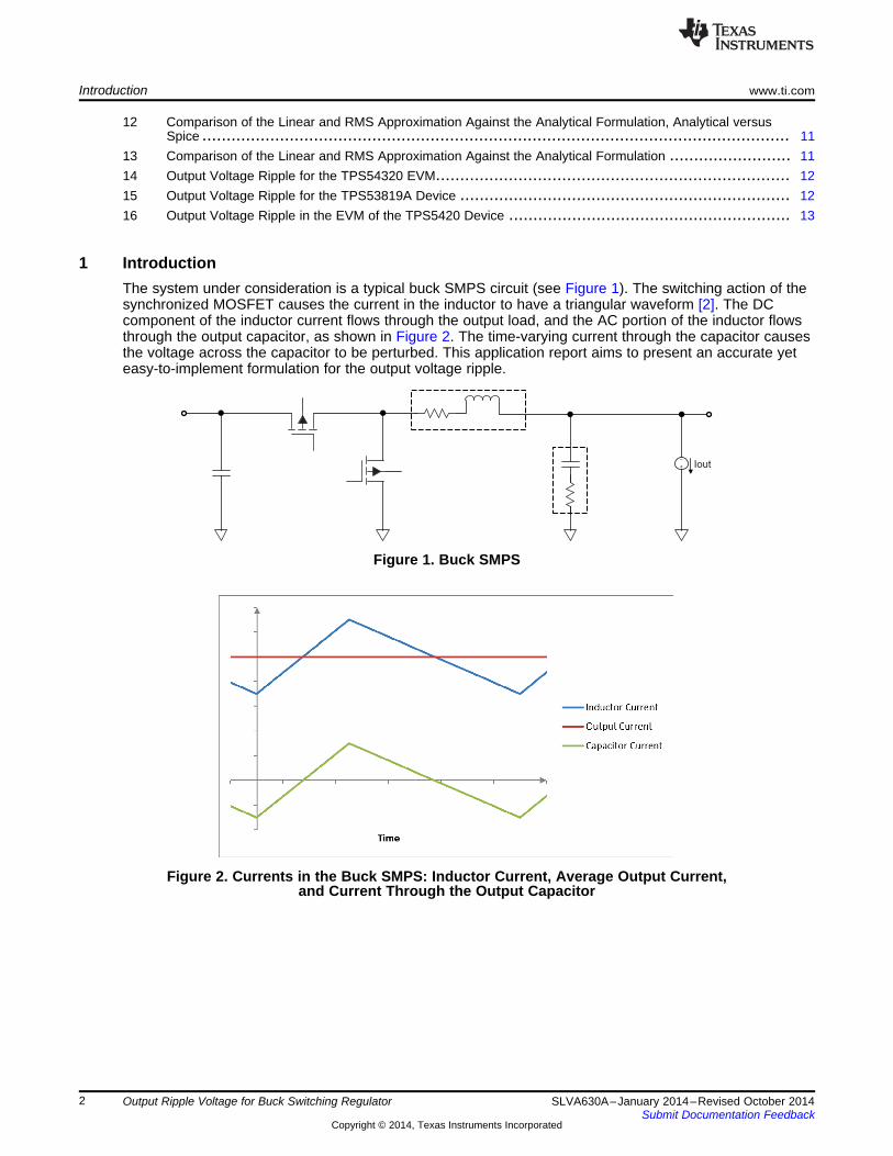
1 IntroductionThe system under consideration is a typical buck SMPS circuit (see Figure 1). The switching action of thesynchronized MOSFET causes the current in the inductor to have a triangular waveform [2]. The DCcomponent of the inductor current flows through the output load, and the AC portion of the inductor flowsthrough the output capacitor, as shown in Figure 2. The time-varying current through the capacitor causesthe voltage across the capacitor to be perturbed. This application report aims to present an accurate yeteasy-to-implement formulation for the output voltage ripple.
Figure 1. Buck SMPS
Figure 2. Currents in the Buck SMPS: Inductor Current, Average Output Current,and Current Through the Output Capacitor
2 Output Ripple Voltage for Buck Switching Regulator SLVA630A–January 2014–Revised October 2014Submit Documentation Feedback
Copyright © 2014, Texas Instruments Incorporated
( ) ( ) ( ) ( )t
I
I I C0
i tv t i t R dt v t 0
C= + + =ò
( ) ( ) ( )R Cv t v t v t= +
( )
( )
p2pI
on
p2p
off
I ti t 1 2
2 T
I t 'i t ' 1 2II 2 T
æ ö= - +ç ÷
è ø
æ ö= -ç ÷
è ø
( ) I onripple
II on sw
,
,
i (t) t 0,Ti t =
i (t) t T ,T
ì Î é ùï ë ûí
Î é ùï ë ûî
( ) ( )0 ripplei t I i t= +
+
–
Iout
i(t)
www.ti.com Output Voltage Ripple Waveform Derivation
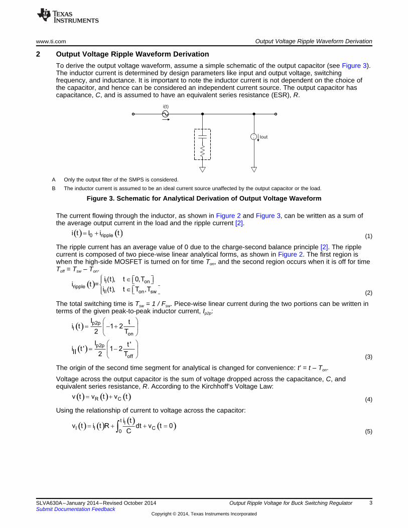
2 Output Voltage Ripple Waveform DerivationTo derive the output voltage waveform, assume a simple schematic of the output capacitor (see Figure 3).The inductor current is determined by design parameters like input and output voltage, switchingfrequency, and inductance. It is important to note the inductor current is not dependent on the choice ofthe capacitor, and hence can be considered an independent current source. The output capacitor hascapacitance, C, and is assumed to have an equivalent series resistance (ESR), R.
A Only the output filter of the SMPS is considered.B The inductor current is assumed to be an ideal current source unaffected by the output capacitor or the load.
Figure 3. Schematic for Analytical Derivation of Output Voltage Waveform
The current flowing through the inductor, as shown in Figure 2 and Figure 3, can be written as a sum ofthe average output current in the load and the ripple current [2].
(1)
The ripple current has an average value of 0 due to the charge-second balance principle [2]. The ripplecurrent is composed of two piece-wise linear analytical forms, as shown in Figure 2. The first region iswhen the high-side MOSFET is turned on for time Ton, and the second region occurs when it is off for timeToff = Tsw – Ton.
(2)
The total switching time is Tsw = 1 / Fsw. Piece-wise linear current during the two portions can be written interms of the given peak-to-peak inductor current, Ip2p:
(3)
The origin of the second time segment for analytical is changed for convenience: t' = t – Ton.
Voltage across the output capacitor is the sum of voltage dropped across the capacitance, C, andequivalent series resistance, R. According to the Kirchhoff’s Voltage Law:
(4)
Using the relationship of current to voltage across the capacitor:
(5)
3SLVA630A–January 2014–Revised October 2014 Output Ripple Voltage for Buck Switching RegulatorSubmit Documentation Feedback
Copyright © 2014, Texas Instruments Incorporated
( ) ( )22
2p2p p2p offout, max II max
off off
I R C I Tv v t ' RC
T 2CT 2
æ öæ öç ÷= = + -ç ÷ç ÷è øè ø
offmax
Tt ' RC
2= -
( )2
p2p p2pII
off off
I It 'v t ' R 1 2 t '
2 T 2C T
æ ö æ ö= - + -ç ÷ ç ÷
è ø è ø
t'
( ) ( )22
2p2p p2p onout,min I min
on on
I R C I Tv v t RC
T 2CT 2
æ öæ öç ÷= = - - -ç ÷ç ÷è øè ø
onmin
Tt RC
2= -
( )I mindv t0
dt=
( ) ( ) ( )tI
I I0
tp2p p2p
0on on
2p2p p2p
on on
i tv t i t R dt
C
I It tR 1 2 1 2
2 T 2C T
I It tR 1 2 t
2 T 2C T
= +
æ ö æ ö= - + + - +ç ÷ ç ÷
è ø è ø
æ öæ ö= - + + - +ç ÷ç ÷ ç ÷è ø è ø
ò
ò
Output Voltage Ripple Waveform Derivation www.ti.com
With no loss of generality, assume the initial voltage on the capacitor is 0. Use the values from Equation 3in Equation 5 to get:
(6)
Equation 6 is quadratic in time; hence, the output voltage waveform has a parabolic shape.
The voltage reaches its minimum at t = tmin, which is obtained by solving the following equation:
(7)
Solving for tmin by using Equation 6 and Equation 7 we obtain:
(8)
Equation 8 states that the minimum is shifted from center of the on time period Ton by the RC timeconstant. Because the minimum time cannot be < 0, it implies that tmin ≥ 0.
The minimum voltage at tmin is:
(9)
Similarly, for the second time segment, output voltage is:
(10)
Whose maximum voltage occurs at:
(11)
Also, because this time cannot be negative, t'max ≥ 0. The maximum voltage is:
(12)
This section established several relationships. First, the waveform of the output ripple is given byEquation 6 and Equation 10. Second, the maximum output voltage is given by Equation 12, and theminimum output voltage is given by Equation 9. Now, the peak-to-peak ripple voltage in various regimescan be evaluated.
4 Output Ripple Voltage for Buck Switching Regulator SLVA630A–January 2014–Revised October 2014Submit Documentation Feedback
Copyright © 2014, Texas Instruments Incorporated
( )sw
out, p2p C R
RCFV V V
2D 1 D
æ ö= + ç ÷ç ÷-è ø
( )
2p2p p2p sw
out, p2psw
I I R C FV
8CF 2 D 1 D= + ×
-
( )
( )
on sw
sw
off sw
sw
on off sw
sw
sw
on off
DT DT
F
1 DT 1 D T
F
1T T T
F
F1 1
T T D 1 D
= =
-= - =
+ = =
+ =-
( ) ( )2 22 2
2 2p2p p2p p2p p2poff onout, p2p
off off on on
I R C I I R C IT TV RC RC
T 2CT 2 T 2CT 2
æ ö æ öæ ö æ öç ÷ ç ÷= + - + + -ç ÷ ç ÷ç ÷ ç ÷è ø è øè ø è ø
on offmin max
T Tt RC 0, and t ' RC 0
2 2= - > = - >
( ) ( )out, p2p II max I minV v t ' v t= -
www.ti.com Output Peak-to-Peak Ripple Voltage
3 Output Peak-to-Peak Ripple VoltageThe output voltage peak-to-peak ripple is the difference between the maximum and minimum of thewaveform:
(13)
The analytical expressions are given in three possible regimes for the output capacitor resistance-capacitance time constant, RC: small, intermediate, and large. The following subsections examine theseregimes.
3.1 Small Resistance-Capacitance CaseWhen the capacitor RC product is small:
(14)
Applying Equation 13, the peak-to-peak output voltage is:
(15)
Noting that:
(16)
Arrive at the expression for output peak-to-peak ripple voltage:
(17)
Often, engineers think in terms of contribution to output ripple due to the capacitor only, or due toresistance only. The capacitor-only portion is obtained by setting equivalent series resistance to 0, R = 0,which gives the familiar expression VC = Ip2p / (8CFsw). If the resistor was alone on the output circuit, thenthe resistor-only portion is VR = Ip2pR. Equation 17 can be written as:
(18)
Comparing Equation 18 with Equation 17 reveals the total output ripple cannot be written in terms of asimple sum of ripple due to the capacitor or resistor alone; other factors such as duty cycle, switchingfrequency, and the values of resistor and capacitor, also play a role. More details are provided in thediscussion of linear approximation in Section 6.
5SLVA630A–January 2014–Revised October 2014 Output Ripple Voltage for Buck Switching RegulatorSubmit Documentation Feedback
Copyright © 2014, Texas Instruments Incorporated
( )22
2p2p p2p p2p onout, p2p
on on
I R I R C I TV RC
2 T 2CT 2
æ öæ öç ÷= + + -ç ÷ç ÷è øè ø
on offT TWhen RC , and RC
2 2< >
( )22
2p2p p2p p2poffout, p2p
off off
I R C I I RTV RC
T 2CT 2 2
æ öæ öç ÷= + - +ç ÷ç ÷è øè ø
on offT TWhen RC , and RC
2 2> <
on offT TRC , and RC
2 2< >
on offT TRC , and RC
2 2> <
( ) ( ) p2p p2pout, p2p II max I min p2p
I R I RV v 0 v t 0t ' I R
2 2
æ ö= = - = = - - =ç ÷ç ÷
è ø
on offT TRC , and RC
2 2> >
Output Peak-to-Peak Ripple Voltage www.ti.com
3.2 Large Resistance-Capacitance CaseWhen the RC product is large:
Use tmin = 0 and t'max = 0 in Equation 6 and Equation 10 to calculate the peak-to-peak output voltage:
(19)
Equation 19 implies that for a large ESR output, voltage ripple is independent of capacitance. Voltageripple is also independent of other variables such as duty cycle and switching frequency.
3.3 Intermediate Resistance-Capacitance CaseWhen the RC product is of an intermediate value, it is either:
(20)
Or
(21)
One extreme of the waveform, either the maximum or minimum voltage, is dependent only on peak-to-peak current and resistance. The other side must be estimated from either Equation 9 orEquation 12.
(22)
(23)
6 Output Ripple Voltage for Buck Switching Regulator SLVA630A–January 2014–Revised October 2014Submit Documentation Feedback
Copyright © 2014, Texas Instruments Incorporated
D = 0.25, C = 10 µF, R = 0 , Ip2p = 2 AFsw = 125 kHz
Ω
D = 0.5, C = 10 µF, R = 0 , Ip2p = 2 AFsw = 125 kHz
Ω
www.ti.com Validation Against SPICE
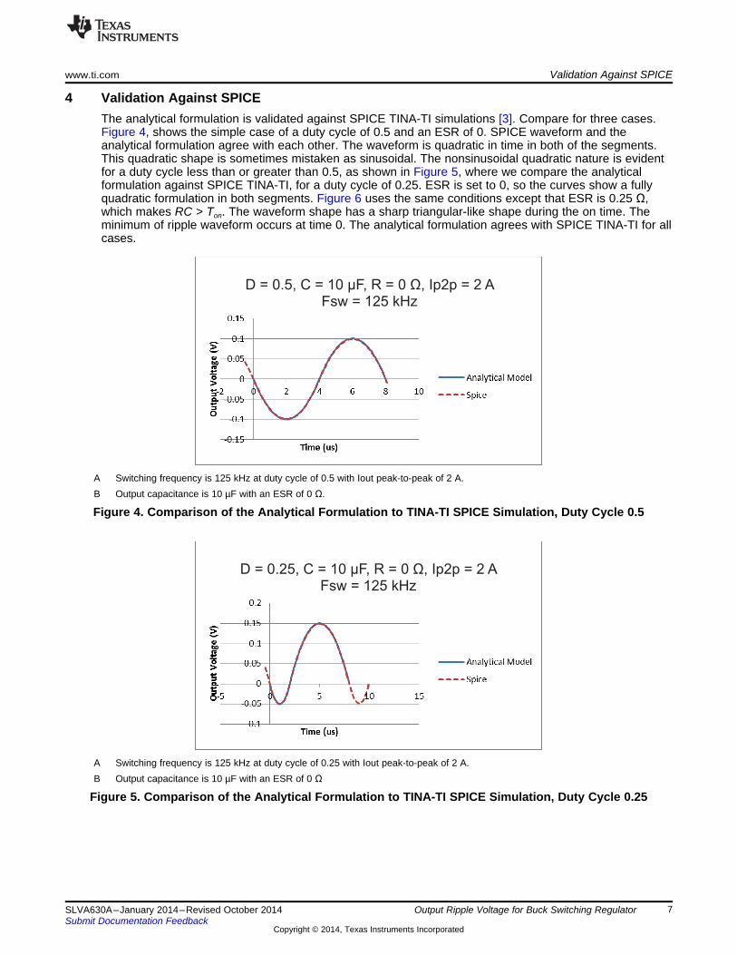
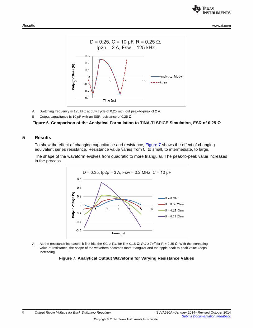
4 Validation Against SPICEThe analytical formulation is validated against SPICE TINA-TI simulations [3]. Compare for three cases.Figure 4, shows the simple case of a duty cycle of 0.5 and an ESR of 0. SPICE waveform and theanalytical formulation agree with each other. The waveform is quadratic in time in both of the segments.This quadratic shape is sometimes mistaken as sinusoidal. The nonsinusoidal quadratic nature is evidentfor a duty cycle less than or greater than 0.5, as shown in Figure 5, where we compare the analyticalformulation against SPICE TINA-TI, for a duty cycle of 0.25. ESR is set to 0, so the curves show a fullyquadratic formulation in both segments. Figure 6 uses the same conditions except that ESR is 0.25 Ω,which makes RC > Ton. The waveform shape has a sharp triangular-like shape during the on time. Theminimum of ripple waveform occurs at time 0. The analytical formulation agrees with SPICE TINA-TI for allcases.
A Switching frequency is 125 kHz at duty cycle of 0.5 with Iout peak-to-peak of 2 A.B Output capacitance is 10 µF with an ESR of 0 Ω.
Figure 4. Comparison of the Analytical Formulation to TINA-TI SPICE Simulation, Duty Cycle 0.5
A Switching frequency is 125 kHz at duty cycle of 0.25 with Iout peak-to-peak of 2 A.B Output capacitance is 10 µF with an ESR of 0 Ω
Figure 5. Comparison of the Analytical Formulation to TINA-TI SPICE Simulation, Duty Cycle 0.25
7SLVA630A–January 2014–Revised October 2014 Output Ripple Voltage for Buck Switching RegulatorSubmit Documentation Feedback
Copyright © 2014, Texas Instruments Incorporated
D = 0.35, Ip2p = 3 A, Fsw = 0.2 MHz, C = 10 µF
D = 0.25, C = 10 R = 0.25 Ω,µF,Ip2p = 2 A, Fsw = 125 kHz
Results www.ti.com
A Switching frequency is 125 kHz at duty cycle of 0.25 with Iout peak-to-peak of 2 A.B Output capacitance is 10 µF with an ESR resistance of 0.25 Ω.
Figure 6. Comparison of the Analytical Formulation to TINA-TI SPICE Simulation, ESR of 0.25 Ω
5 ResultsTo show the effect of changing capacitance and resistance, Figure 7 shows the effect of changingequivalent series resistance. Resistance value varies from 0, to small, to intermediate, to large.
The shape of the waveform evolves from quadratic to more triangular. The peak-to-peak value increasesin the process.
A As the resistance increases, it first hits the RC ≥ Ton for R = 0.15 Ω; RC ≥ Toff for R = 0.35 Ω. With the increasingvalue of resistance, the shape of the waveform becomes more triangular and the ripple peak-to-peak value keepsincreasing.
Figure 7. Analytical Output Waveform for Varying Resistance Values
8 Output Ripple Voltage for Buck Switching Regulator SLVA630A–January 2014–Revised October 2014Submit Documentation Feedback
Copyright © 2014, Texas Instruments Incorporated
Analytical versus SPICEC = 100 µF, Fsw = 167 kHz, D = 0.167, Ipp = 2 A
D = 0.35, Ip2p = 3 A, Fsw = 0.2 MHz, R = 0.05 Ω
www.ti.com Results
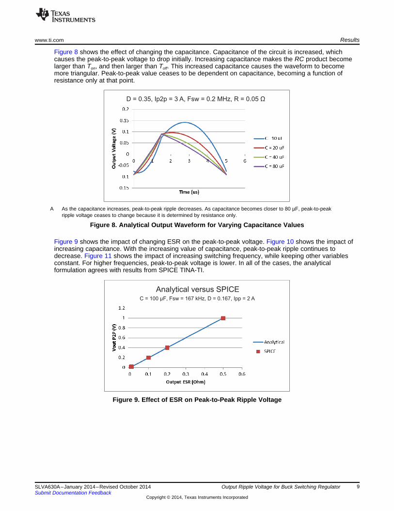
Figure 8 shows the effect of changing the capacitance. Capacitance of the circuit is increased, whichcauses the peak-to-peak voltage to drop initially. Increasing capacitance makes the RC product becomelarger than Ton, and then larger than Toff. This increased capacitance causes the waveform to becomemore triangular. Peak-to-peak value ceases to be dependent on capacitance, becoming a function ofresistance only at that point.
A As the capacitance increases, peak-to-peak ripple decreases. As capacitance becomes closer to 80 µF, peak-to-peakripple voltage ceases to change because it is determined by resistance only.
Figure 8. Analytical Output Waveform for Varying Capacitance Values
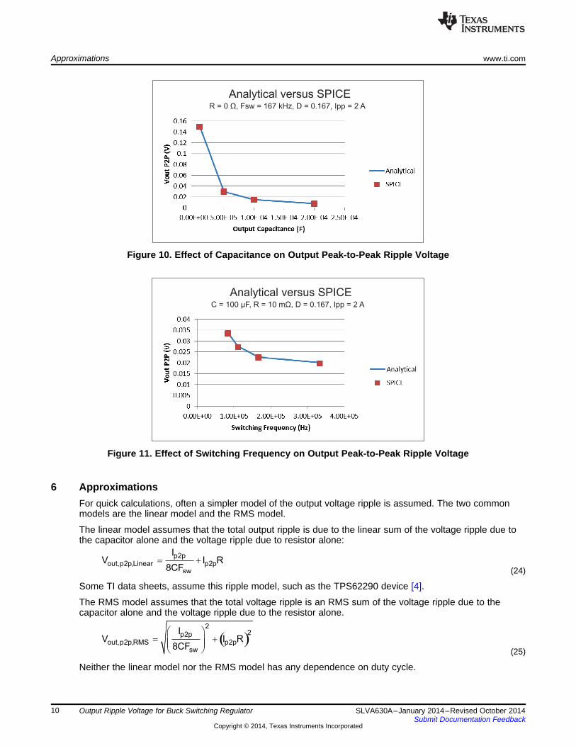
Figure 9 shows the impact of changing ESR on the peak-to-peak voltage. Figure 10 shows the impact ofincreasing capacitance. With the increasing value of capacitance, peak-to-peak ripple continues todecrease. Figure 11 shows the impact of increasing switching frequency, while keeping other variablesconstant. For higher frequencies, peak-to-peak voltage is lower. In all of the cases, the analyticalformulation agrees with results from SPICE TINA-TI.
Figure 9. Effect of ESR on Peak-to-Peak Ripple Voltage
9SLVA630A–January 2014–Revised October 2014 Output Ripple Voltage for Buck Switching RegulatorSubmit Documentation Feedback
Copyright © 2014, Texas Instruments Incorporated
( )2
2p2pout, p2p,RMS p2p
sw
IV I R
8CF
æ ö= +ç ÷ç ÷
è ø
p2pout, p2p,Linear p2p
sw
IV I R
8CF= +
Analytical versus SPICEC = 100 µF, R = 10 mΩ, D = 0.167, Ipp = 2 A
Analytical versus SPICER = 0 Ω, Fsw = 167 kHz, D = 0.167, Ipp = 2 A
Approximations www.ti.com
Figure 10. Effect of Capacitance on Output Peak-to-Peak Ripple Voltage
Figure 11. Effect of Switching Frequency on Output Peak-to-Peak Ripple Voltage
6 ApproximationsFor quick calculations, often a simpler model of the output voltage ripple is assumed. The two commonmodels are the linear model and the RMS model.
The linear model assumes that the total output ripple is due to the linear sum of the voltage ripple due tothe capacitor alone and the voltage ripple due to resistor alone:
(24)
Some TI data sheets, assume this ripple model, such as the TPS62290 device [4].
The RMS model assumes that the total voltage ripple is an RMS sum of the voltage ripple due to thecapacitor alone and the voltage ripple due to the resistor alone.
(25)
Neither the linear model nor the RMS model has any dependence on duty cycle.
10 Output Ripple Voltage for Buck Switching Regulator SLVA630A–January 2014–Revised October 2014Submit Documentation Feedback
Copyright © 2014, Texas Instruments Incorporated
C = 10 µF, Fsw = 1 MHz, Ipp = 2 A, D = 0.5
Analytical versus SPICEC = 100 µF, R = 10 mΩ, Fsw = 167 kHz, Ipp = 2 A
www.ti.com Approximations
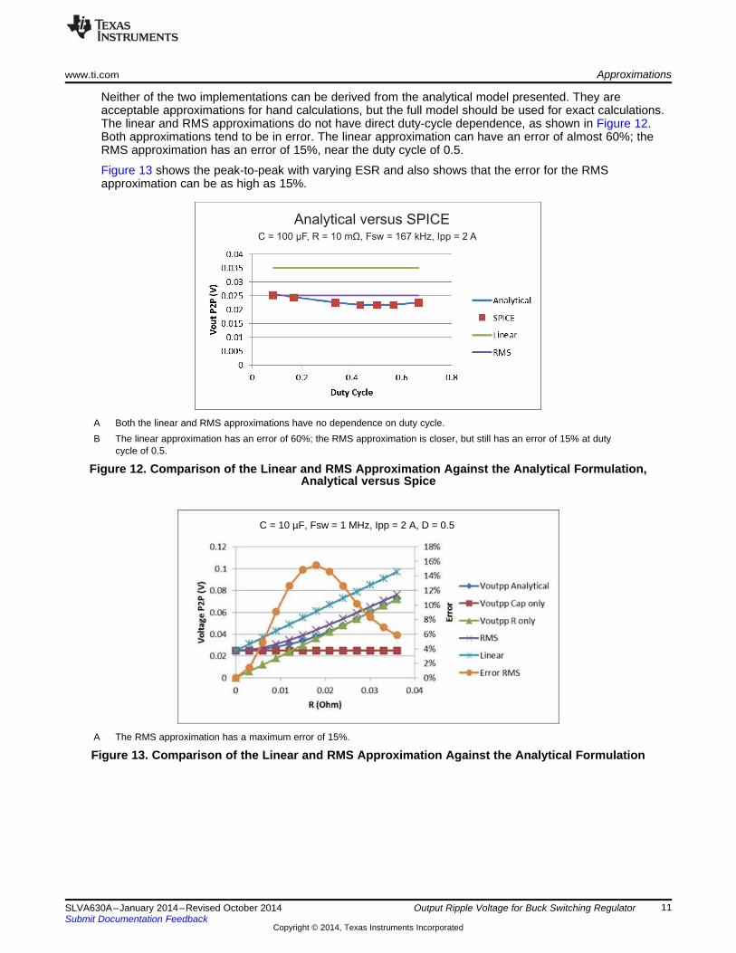
Neither of the two implementations can be derived from the analytical model presented. They areacceptable approximations for hand calculations, but the full model should be used for exact calculations.The linear and RMS approximations do not have direct duty-cycle dependence, as shown in Figure 12.Both approximations tend to be in error. The linear approximation can have an error of almost 60%; theRMS approximation has an error of 15%, near the duty cycle of 0.5.
Figure 13 shows the peak-to-peak with varying ESR and also shows that the error for the RMSapproximation can be as high as 15%.
A Both the linear and RMS approximations have no dependence on duty cycle.B The linear approximation has an error of 60%; the RMS approximation is closer, but still has an error of 15% at duty
cycle of 0.5.
Figure 12. Comparison of the Linear and RMS Approximation Against the Analytical Formulation,Analytical versus Spice
A The RMS approximation has a maximum error of 15%.
Figure 13. Comparison of the Linear and RMS Approximation Against the Analytical Formulation
11SLVA630A–January 2014–Revised October 2014 Output Ripple Voltage for Buck Switching RegulatorSubmit Documentation Feedback
Copyright © 2014, Texas Instruments Incorporated
Examples from TI Devices and Evaluation Modules (EVMs) www.ti.com
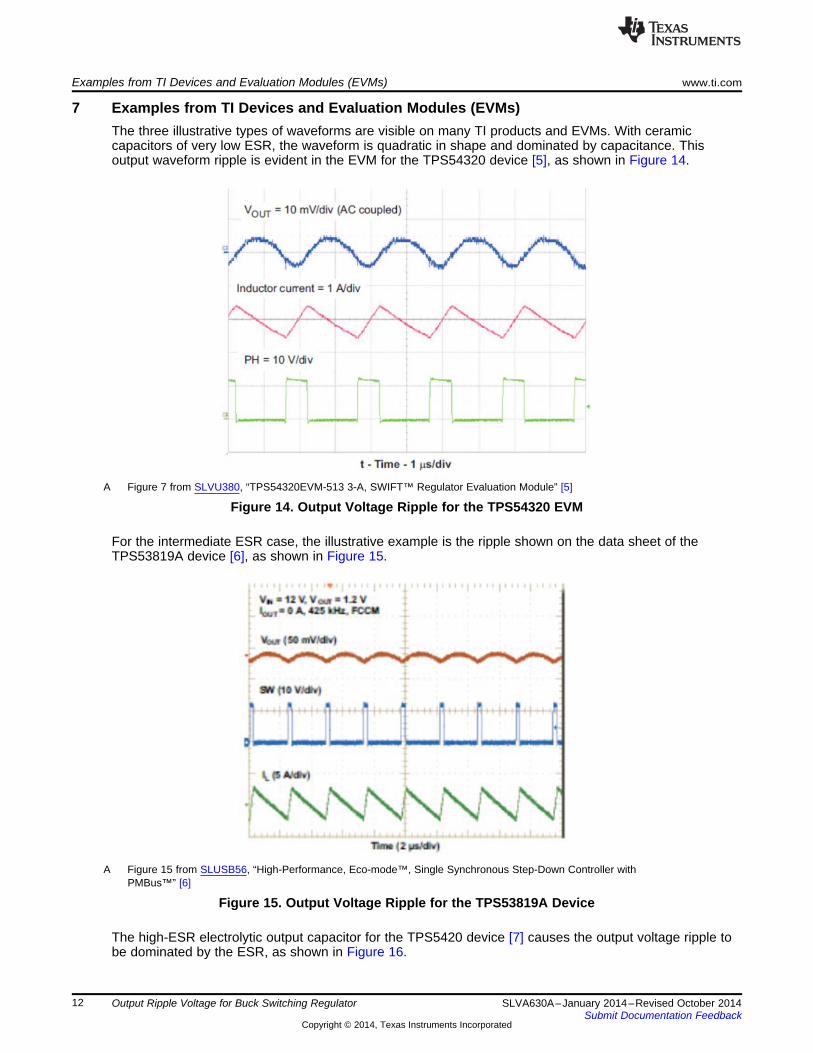
7 Examples from TI Devices and Evaluation Modules (EVMs)The three illustrative types of waveforms are visible on many TI products and EVMs. With ceramiccapacitors of very low ESR, the waveform is quadratic in shape and dominated by capacitance. Thisoutput waveform ripple is evident in the EVM for the TPS54320 device [5], as shown in Figure 14.
A Figure 7 from SLVU380, “TPS54320EVM-513 3-A, SWIFT™ Regulator Evaluation Module” [5]
Figure 14. Output Voltage Ripple for the TPS54320 EVM
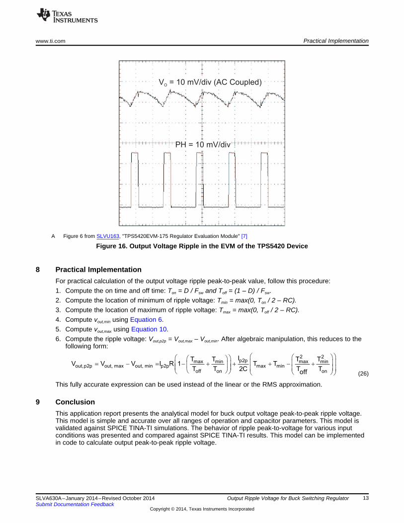
For the intermediate ESR case, the illustrative example is the ripple shown on the data sheet of theTPS53819A device [6], as shown in Figure 15.
A Figure 15 from SLUSB56, “High-Performance, Eco-mode™, Single Synchronous Step-Down Controller withPMBus™” [6]
Figure 15. Output Voltage Ripple for the TPS53819A Device
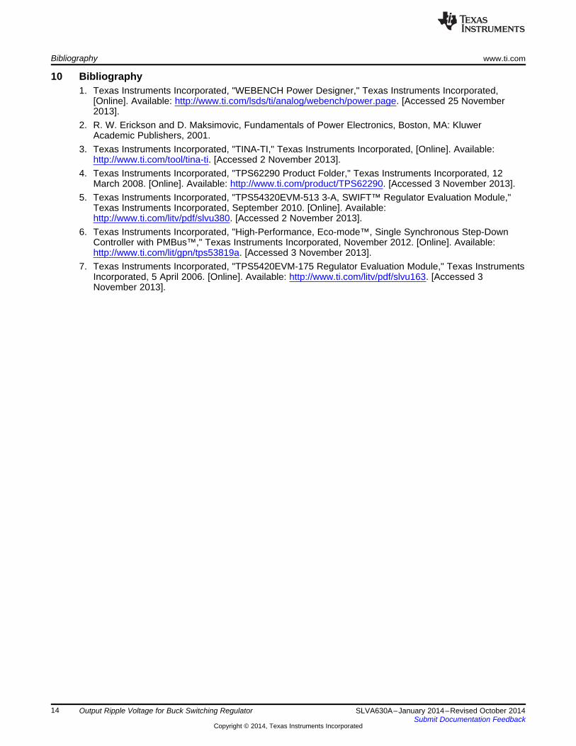
The high-ESR electrolytic output capacitor for the TPS5420 device [7] causes the output voltage ripple tobe dominated by the ESR, as shown in Figure 16.
12 Output Ripple Voltage for Buck Switching Regulator SLVA630A–January 2014–Revised October 2014Submit Documentation Feedback
Copyright © 2014, Texas Instruments Incorporated
2 2p2pmax maxmin min
out, p2p out, max out, min p2p max minoff on on
IT TT TV V V I R 1 T T
T T 2C T Toff
æ öæ öæ öæ öç ÷ç ÷= - = - + + + - +ç ÷ç ÷ç ÷ ç ÷ç ÷è øè ø è øè ø
V = 10 mV/div (AC Coupled)O
PH = 10 mV/div
www.ti.com Practical Implementation
A Figure 6 from SLVU163, "TPS5420EVM-175 Regulator Evaluation Module" [7]
Figure 16. Output Voltage Ripple in the EVM of the TPS5420 Device
8 Practical ImplementationFor practical calculation of the output voltage ripple peak-to-peak value, follow this procedure:1. Compute the on time and off time: Ton = D / Fsw and Toff = (1 – D) / Fsw.2. Compute the location of minimum of ripple voltage: Tmin = max(0, Ton / 2 – RC).3. Compute the location of maximum of ripple voltage: Tmax = max(0, Toff / 2 – RC).4. Compute vout,min using Equation 6.5. Compute vout,max using Equation 10.6. Compute the ripple voltage: Vout,p2p = Vout,max – Vout,min. After algebraic manipulation, this reduces to the
following form:
(26)
This fully accurate expression can be used instead of the linear or the RMS approximation.
9 ConclusionThis application report presents the analytical model for buck output voltage peak-to-peak ripple voltage.This model is simple and accurate over all ranges of operation and capacitor parameters. This model isvalidated against SPICE TINA-TI simulations. The behavior of ripple peak-to-voltage for various inputconditions was presented and compared against SPICE TINA-TI results. This model can be implementedin code to calculate output peak-to-peak ripple voltage.
13SLVA630A–January 2014–Revised October 2014 Output Ripple Voltage for Buck Switching RegulatorSubmit Documentation Feedback
Copyright © 2014, Texas Instruments Incorporated
Bibliography www.ti.com
10 Bibliography1. Texas Instruments Incorporated, "WEBENCH Power Designer," Texas Instruments Incorporated,
[Online]. Available: http://www.ti.com/lsds/ti/analog/webench/power.page. [Accessed 25 November2013].
2. R. W. Erickson and D. Maksimovic, Fundamentals of Power Electronics, Boston, MA: KluwerAcademic Publishers, 2001.
3. Texas Instruments Incorporated, "TINA-TI," Texas Instruments Incorporated, [Online]. Available:http://www.ti.com/tool/tina-ti. [Accessed 2 November 2013].
4. Texas Instruments Incorporated, "TPS62290 Product Folder," Texas Instruments Incorporated, 12March 2008. [Online]. Available: http://www.ti.com/product/TPS62290. [Accessed 3 November 2013].
5. Texas Instruments Incorporated, "TPS54320EVM-513 3-A, SWIFT™ Regulator Evaluation Module,"Texas Instruments Incorporated, September 2010. [Online]. Available:http://www.ti.com/litv/pdf/slvu380. [Accessed 2 November 2013].
6. Texas Instruments Incorporated, "High-Performance, Eco-mode™, Single Synchronous Step-DownController with PMBus™," Texas Instruments Incorporated, November 2012. [Online]. Available:http://www.ti.com/lit/gpn/tps53819a. [Accessed 3 November 2013].
7. Texas Instruments Incorporated, "TPS5420EVM-175 Regulator Evaluation Module," Texas InstrumentsIncorporated, 5 April 2006. [Online]. Available: http://www.ti.com/litv/pdf/slvu163. [Accessed 3November 2013].
14 Output Ripple Voltage for Buck Switching Regulator SLVA630A–January 2014–Revised October 2014Submit Documentation Feedback
Copyright © 2014, Texas Instruments Incorporated

www.ti.com Revision History
Revision History
Changes from Original (January 2014) to A Revision .................................................................................................... Page
• Updated Equation 8, replaced 'R' with 'RC'............................................................................................ 4
15SLVA630A–January 2014–Revised October 2014 Revision HistorySubmit Documentation Feedback
Copyright © 2014, Texas Instruments Incorporated

IMPORTANT NOTICE
Texas Instruments Incorporated and its subsidiaries (TI) reserve the right to make corrections, enhancements, improvements and otherchanges to its semiconductor products and services per JESD46, latest issue, and to discontinue any product or service per JESD48, latestissue. Buyers should obtain the latest relevant information before placing orders and should verify that such information is current andcomplete. All semiconductor products (also referred to herein as “components”) are sold subject to TI’s terms and conditions of salesupplied at the time of order acknowledgment.TI warrants performance of its components to the specifications applicable at the time of sale, in accordance with the warranty in TI’s termsand conditions of sale of semiconductor products. Testing and other quality control techniques are used to the extent TI deems necessaryto support this warranty. Except where mandated by applicable law, testing of all parameters of each component is not necessarilyperformed.TI assumes no liability for applications assistance or the design of Buyers’ products. Buyers are responsible for their products andapplications using TI components. To minimize the risks associated with Buyers’ products and applications, Buyers should provideadequate design and operating safeguards.TI does not warrant or represent that any license, either express or implied, is granted under any patent right, copyright, mask work right, orother intellectual property right relating to any combination, machine, or process in which TI components or services are used. Informationpublished by TI regarding third-party products or services does not constitute a license to use such products or services or a warranty orendorsement thereof. Use of such information may require a license from a third party under the patents or other intellectual property of thethird party, or a license from TI under the patents or other intellectual property of TI.Reproduction of significant portions of TI information in TI data books or data sheets is permissible only if reproduction is without alterationand is accompanied by all associated warranties, conditions, limitations, and notices. TI is not responsible or liable for such altereddocumentation. Information of third parties may be subject to additional restrictions.Resale of TI components or services with statements different from or beyond the parameters stated by TI for that component or servicevoids all express and any implied warranties for the associated TI component or service and is an unfair and deceptive business practice.TI is not responsible or liable for any such statements.Buyer acknowledges and agrees that it is solely responsible for compliance with all legal, regulatory and safety-related requirementsconcerning its products, and any use of TI components in its applications, notwithstanding any applications-related information or supportthat may be provided by TI. Buyer represents and agrees that it has all the necessary expertise to create and implement safeguards whichanticipate dangerous consequences of failures, monitor failures and their consequences, lessen the likelihood of failures that might causeharm and take appropriate remedial actions. Buyer will fully indemnify TI and its representatives against any damages arising out of the useof any TI components in safety-critical applications.In some cases, TI components may be promoted specifically to facilitate safety-related applications. With such components, TI’s goal is tohelp enable customers to design and create their own end-product solutions that meet applicable functional safety standards andrequirements. Nonetheless, such components are subject to these terms.No TI components are authorized for use in FDA Class III (or similar life-critical medical equipment) unless authorized officers of the partieshave executed a special agreement specifically governing such use.Only those TI components which TI has specifically designated as military grade or “enhanced plastic” are designed and intended for use inmilitary/aerospace applications or environments. Buyer acknowledges and agrees that any military or aerospace use of TI componentswhich have not been so designated is solely at the Buyer's risk, and that Buyer is solely responsible for compliance with all legal andregulatory requirements in connection with such use.TI has specifically designated certain components as meeting ISO/TS16949 requirements, mainly for automotive use. In any case of use ofnon-designated products, TI will not be responsible for any failure to meet ISO/TS16949.
Products ApplicationsAudio www.ti.com/audio Automotive and Transportation www.ti.com/automotiveAmplifiers amplifier.ti.com Communications and Telecom www.ti.com/communicationsData Converters dataconverter.ti.com Computers and Peripherals www.ti.com/computersDLP® Products www.dlp.com Consumer Electronics www.ti.com/consumer-appsDSP dsp.ti.com Energy and Lighting www.ti.com/energyClocks and Timers www.ti.com/clocks Industrial www.ti.com/industrialInterface interface.ti.com Medical www.ti.com/medicalLogic logic.ti.com Security www.ti.com/securityPower Mgmt power.ti.com Space, Avionics and Defense www.ti.com/space-avionics-defenseMicrocontrollers microcontroller.ti.com Video and Imaging www.ti.com/videoRFID www.ti-rfid.comOMAP Applications Processors www.ti.com/omap TI E2E Community e2e.ti.comWireless Connectivity www.ti.com/wirelessconnectivity
Mailing Address: Texas Instruments, Post Office Box 655303, Dallas, Texas 75265Copyright © 2014, Texas Instruments Incorporated