Embed Size (px)
Citation preview

A TWO-PHASE BUCK CONVERTER WITH OPTIMUM PHASE
SELECTION FOR LOW POWER APPLICATIONS
TAYLOR CRAIG YEAGO
Thesis submitted to the faculty of the Virginia Polytechnic Institute and State University
in partial fulfillment of the requirements for the degree of
Master of Science
In
Electrical Engineering
Dong S. Ha, Co-Chair
Qiang Li, Co-Chair
Kwang-Jin Koh
December 10, 2014
Blacksburg, VA
Keywords: Synchronous Buck Converter, Constant ON-Time Control, Optimum Phase
Selection, Light-load efficiency, Pulse Frequency Modulation
Copyright 2014, Taylor Craig Yeago

A Two-Phase Buck Converter with Optimum Phase Selection for Low Power
Applications
Taylor Craig Yeago
ABSTRACT
Power consumption of smart cameras varies significantly between sleep mode and active
mode, and a smart camera operates in sleep mode for 80 – 90% of time for typical use. To prolong
the battery life of smart cameras, it is essential to increase the power converter efficiency for light
load, while being able to manage heavy load. The power stage of traditional buck converter is
optimized for maximum load, at the cost of light-load efficiency. Wei proposed a multiphase buck
converter incorporating the baby-buck concept and optimum number of phases (ONP) control.
This thesis research investigated Wei’s multiphase buck converter to improve the light-load
efficiency for smart cameras as the target application.
The proposed two-phase buck converter aims to provide power for microprocessors of smart
cameras. The input voltage of the converter is 5 V DC, and the output voltage is 1.2 V DC with
power dissipation range of 25 mA (30 mW) for light load and 833 mA (1 W) for heavy load. Three
methods are considered to improve light-load efficiency: adopting baby-buck concept, adapting
ONP control for low-power range, and implementing a pulse frequency modulation (PFM) control
scheme with discontinuous conduction mode (DCM) to lower switching frequency. The first
method is to adopt the baby-buck concept through power stage design of each phase to optimize
efficiency for a specific load range. The baby-buck phase is optimized for light load and the heavy-
load phase is designed to handle the processors maximum power consumption. The second method
performs phase selection from sensed load current information. Rather than have all phases active
for heavy-load as in ONP control, optimum phase selection (OPS) control is introduced to
adaptively select between phases based on load current. Due to low-power constraints, OPS is
more efficient for the medium to heavy-load range. The transition between phases due to load

iii
change is also investigated. The third and final method implements PFM control with DCM to
lower switching frequency and reduce switching and driving losses under light load. PFM is
accomplished with a constant on-time (COT) valley current mode controller, which uses the
inductor current information and output voltage to generate switching signals for both the top and
bottom switches. The baby-buck phase enters DCM to lower switching frequency under very light
load, while the heavy-load phase remains in continuous conduction mode (CCM) throughout its
load range.
The proposed two-phase buck converter is designed and prototyped using discrete
components. Efficiency of the two-phase converter and a power loss breakdown for each block in
the control scheme were measured. The efficiency ranges from 64% to 81% for light load ranging
of 30 mW to 200 mW, and the efficiency ranges from 81% to 88% for heavy load ranging from
200 mW to 1 W. The majority loss is due to controllers, which are responsible for 37 % (8.6 mW)
for light load of 60 mW and for 10.9 % (9 mW) for heavy load of 600 mW. The gate driver loss is
considerable for heavy load of 600 mW, consuming 11.9% (9.8mW). The converter has a 10 mV
overshoot voltage for a load step-down from 225 mA to 25 mA, and it has 65 mV overshoot voltage
for a load step-up from 25 mA to 225 mA. Although, a fair comparison is difficult due to use of
discrete parts for OPS control, the proposed converter shows reasonably good efficiency and
performance.

iv
Acknowledgements
I would like to offer my appreciation to my principle advisor, Dr. Dong S. Ha, who has
guided me and given direction throughout my thesis with his advice and knowledge. I would like
to thank Dr. Qiang Li for his guidance, expert knowledge, and familiarity in my thesis research. I
would like to thank Kwang-Jin Koh for being part of my advisory committee and his support.
This work was supported in part by the Center for Integrated Smart Sensors funded by the
Korea Ministry of Science, ICT & Future Planning as Global Frontier Project (CISS-2-3).
I would like to thank Virginia Tech for its teaching assistant opportunities to provide
scholarship and funding throughout. In addition, I would like to thank Linear Technology, Texas
Instruments, and Coilcraft for providing sample components for my prototype. I would like to
thank CPES for allowing the use of lab equipment for testing.
I would like to thank my colleagues, Brian Cassidy, Ross Kerely, Ji Hoon Hyun, and
Thomas O’Connor. It was a great pleasure working with them during my Master’s study. Also,
many thanks go to my colleagues with the MICS group for their support and encouragement.
Special thanks go to my girlfriend, Emily Swain, for her support and friendship throughout
my time in graduate school. Thanks to all my friends at Virginia Tech. Life at Virginia Tech would
not have been the same without everyone around.
Finally, I am also extremely grateful to my parents, sister and brothers for their
unconditional support and patience.

v
Table of Contents
1.1 MOTIVATION ................................................................................................................... 1
1.2 STEP-DOWN DC/DC CONVERTERS .................................................................................. 1
1.3 MULITPHASE CONVERTER WITH IMPROVED LIGHT-LOAD EFFICIENCY ........................... 3
1.4 TECHNICAL CONTRIBUTIONS OF THE PROPOSED RESEARCH ............................................ 3
1.5 ORGANIZATION OF THE THESIS ....................................................................................... 4
2.1 DESIGN REQUIREMENTS .................................................................................................. 5
2.2 PREVIOUS SYNCHRONOUS BUCK CONVERTER APPROACH .............................................. 6
2.2.1 Synchronous Buck Control for Light-Load ............................................................ 7
2.2.2 Shortcomings .......................................................................................................... 8
2.3 WEI’S MULTIPHASE CONVERTER WITH BABY-BUCK ...................................................... 9
2.3.1 ONP Control and Baby-buck Concept .................................................................... 9
2.3.1.1 Optimum Number of Phases Control ........................................................... 10
2.3.1.2 Baby-Buck Concept ..................................................................................... 11
2.3.2 Shortcomings of Wei’s Design ............................................................................. 12

vi
2.4 CONSTANT ON-TIME CONTROL ..................................................................................... 13
2.5 OPTIMUM PHASE SELECTION CONTROL ........................................................................ 16
2.6 CHAPTER SUMMARY ..................................................................................................... 17
3.1 CIRCUIT SCHEMATIC AND BLOCK DIAGRAM ................................................................. 19
3.2 CONTROL BLOCK DIAGRAM AND CONTROLLER CIRCUIT .............................................. 21
3.2.1 Switching Control ................................................................................................. 22
3.2.2 Phase Selection and Transition ............................................................................. 25
3.3 COMPONENT DESIGN AND SELECTION ........................................................................... 30
3.4 CHAPTER SUMMARY ..................................................................................................... 38
4.1 PROTOTYPE DESIGN PROCEDURE .................................................................................. 39
4.1.1 Open-Loop Prototype and Simulations ................................................................. 39
4.1.2 Closed-Loop Prototype and Simulations .............................................................. 43
4.1.2.1 First Version................................................................................................. 43
4.1.2.2 Second Version ............................................................................................ 44
4.1.2.3 Final Version ................................................................................................ 48
4.2 MEASUREMENT SETUP .................................................................................................. 49
4.3 MEASUREMENT RESULTS .............................................................................................. 52
4.3.1 Transient Waveforms ............................................................................................ 52
4.3.1.1 Light Load .................................................................................................... 52
4.3.1.2 Heavy Load .................................................................................................. 55
4.3.2 Efficiency and Loss Breakdown ........................................................................... 56

vii
4.3.2.1 Overall Efficiency ........................................................................................ 56
4.3.2.2 Power Loss Breakdown ............................................................................... 58
4.3.3 Load Transient Performance ................................................................................. 60
4.4 FUTURE IMPROVEMENTS ............................................................................................... 64
4.4.1 Discrete Prototype ................................................................................................. 64
4.4.2 Integration of Controller ....................................................................................... 65
4.5 CHAPTER SUMMARY ..................................................................................................... 65

viii
List of Figures
Figure 1.1: Block diagram for a power converter system proposed by N. Mohan, T. M.
Undeland, and W. P. Robbins, Power Electronics: Converters, Applications, and Design, 3rd
ed. New Jersey: John Wiley & Sons Inc., 2003. Used under fair use, 2014. .......................... 2
Figure 1.2: Load profile for typical microprocessor proposed in lecture by Q. Li. ECE 5254.
Class Lecture, Topic: “Chapter 5: new current-mode control modeling based on describing
function method.” Bradley Dept. of Electrical and Computer Engineering, Virginia Tech,
Blacksburg, VA, Fall 2013. Used under fair use, 2014. .......................................................... 2
Figure 2.1: Power block diagram for target smart camera system, thesis contribution (orange) ... 6
Figure 2.2: PFM signal with respect to load current variation proposed by V. G. Madhuravasal,
“Extreme Temperature Switch Mode Power Supply based on Vee-square Control Using
Silicon Carbide, Silicon on Sapphire, Hybrid Technology.” Ph.D. dissertation, ECE,
Oklahoma State University, Stillwater, OK, 2009. Used under fair use, 2014. ...................... 7
Figure 2.3: Switching frequency and efficiency versus load current proposed by X. Zhou, M.
Donati, L. Amoroso, and F. C. Lee, “Improved Light-Load Efficiency for Synchronous
Rectifier Voltage Regulator Module,” IEEE Transactions on Power Electronics, vol. 15, no.
5, pp. 826-834, Sept. 2000. Used under fair use, 2014. .......................................................... 7
Figure 2.4: Multiphase converter with baby-buck phase proposed by J. Wei, “High frequency
high-efficiency voltage regulators for future microprocessors,” PhD Dissertation,
Department of Electrical and Computer Engineering, Virginia Tech, 2004. Used under fair
use, 2014. ............................................................................................................................... 10
Figure 2.5: Experimental efficiency improvement of the ONP control proposed by J. Wei, “High
frequency high-efficiency voltage regulators for future microprocessors,” PhD Dissertation,
Department of Electrical and Computer Engineering, Virginia Tech, 2004. Used under fair
use, 2014. ............................................................................................................................... 11
Figure 2.6: Efficiency comparison with and without baby-buck concept proposed by J. Wei,
“High frequency high-efficiency voltage regulators for future microprocessors,” PhD

ix
Dissertation, Department of Electrical and Computer Engineering, Virginia Tech, 2004.
Used under fair use, 2014. ..................................................................................................... 12
Figure 2.7: Valley current mode COT control schematic proposed in lecture by Q. Li, “Chapter 5
– New Current-Mode Control Modeling based on Describing Function Method.” Bradley
Department of Electrical and Computer Engineering, Virginia Tech, Blacksburg, VA, Slide
V-11, Fall 2013. ..................................................................................................................... 15
Figure 2.8: Valley current mode COT control waveforms under CCM ....................................... 15
Figure 2.9: Valley current mode COT control waveforms under DCM ....................................... 16
Figure 3.1: Block diagram of the proposed two-phase buck converter ........................................ 20
Figure 3.2: Schematic of the proposed two-phase buck converter ............................................... 21
Figure 3.3: Control signals for baby-buck (DCM) and heavy-load (CCM) phases...................... 22
Figure 3.4: Control Scheme for baby-buck phase of the proposed converter in SIMPLIS .......... 23
Figure 3.5: Controller of the proposed converter with discrete parts ........................................... 24
Figure 3.6: High-side load current sensing configuration ............................................................ 26
Figure 3.7: Simulated total loop gain bode plot for control loop in LTPowerCAD II for (a) baby-
buck phase (b) heavy-load phase ........................................................................................... 27
Figure 3.8: Load step up with 40us overlap delay transient performance .................................... 28
Figure 3.9: Load step-down with overlap of ten switching cycles (40 µs) under both phases
active...................................................................................................................................... 29
Figure 3.10: Load step down comparison using overlap: Output voltage overshoot with overlap
in red and without overlap (immediate transition) in green .................................................. 29
Figure 3.11: Inductor current waveforms during load step up and down transition .................... 30
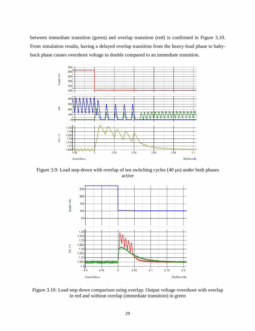
Figure 3.12: Efficiency (MOSFET losses only) in MATLAB with ideal MOSFET design ........ 34
Figure 3.13: MOSFET loss breakdown of baby-buck phase with Case 1 – Si1012r and Case 2 –
CSD15571Q2 ........................................................................................................................ 35

x
Figure 3.14: MOSFET loss breakdown of heavy-load phase with Case 1 – CSD15571Q2 and
Case 2 – CSD13202Q2 .......................................................................................................... 36
Figure 3.15: MOSFET loss breakdown of baby-buck phase, designed MOSFETS vs. selected
discrete parts .......................................................................................................................... 37
Figure 3.16: MOSFET loss breakdown of heavy-load phase, designed MOSFETS vs. selected
discrete parts .......................................................................................................................... 38
Figure 4.1: Open-loop prototype of both phases with discrete components................................. 40
Figure 4.2: Open-loop baby-buck phase efficiency: prototype measurement vs. simulation ....... 41
Figure 4.3: Open-loop heavy-load phase efficiency: prototype measurement vs. simulation ...... 41
Figure 4.4: Open-loop two-phase converter prototype efficiency ................................................ 42
Figure 4.5: First version of closed-loop prototype with discrete components .............................. 43
Figure 4.6: Overall efficiency of closed-loop prototype, first version ......................................... 44
Figure 4.7: LTspice simulation demonstrating transition between phases due to load steps ....... 45
Figure 4.8: Second version of closed-loop prototype with discrete components ......................... 46
Figure 4.9: Overall efficiency of closed-loop prototype, second version ..................................... 47
Figure 4.10: Final closed-loop prototype with discrete components ............................................ 49
Figure 4.11: Test setup for efficiency measurements ................................................................... 51
Figure 4.12: Test setup for load transient measurements ............................................................. 52
Figure 4.13: Baby-buck top gate voltage with 150 mW load, CCM ............................................ 53
Figure 4.14: Baby-buck top gate voltage with 60 mW load, DCM .............................................. 53
Figure 4.15: Baby-buck top gate voltage with 30 mW load, DCM .............................................. 54
Figure 4.16: Output voltage ripple with 30 mW load, DCM ........................................................ 55
Figure 4.17: Heavy-load phase top gate voltage with 240 mW load, CCM ................................. 55
Figure 4.18: Output voltage ripple with 240 mW load, CCM ...................................................... 56
Figure 4.19: Overall Efficiency of the proposed two-phase converter final prototype ................ 57

xi
Figure 4.20: Efficiency of LTC3809 buck converter proposed by Linear Technology, “No
Rsense, Low EMI, Synchronous DC/DC Controller,” LTC3809 datasheet. [Online].
Available: http://cds.linear.com/docs/en/datasheet/3809fc.pdf. [Accessed: 8-Dec-2014].
Used under fair use, 2014. ..................................................................................................... 58
Figure 4.21: Power loss breakdown of prototype two-phase converter: 60 mW and 600 mW load
............................................................................................................................................... 59
Figure 4.22: Percentage loss breakdown of prototype two-phase converter: 60 mW and 600 mW
load ........................................................................................................................................ 60
Figure 4.23: Load-transient performance from 200 mA load step down, output voltage (yellow),
load current (blue), baby-buck phase control signal (pink), and heavy-load phase control
signal (green) ......................................................................................................................... 61
Figure 4.24: Load-transient performance from 200 mA load step down, baby-buck phase control
signal (green), heavy-load phase inductor current (yellow), and baby-buck phase inductor
current (purple) ...................................................................................................................... 62
Figure 4.25: Load-transient performance from 200 mA load step up, output voltage (yellow),
load current (blue), baby-buck phase control signal (pink), and heavy-load phase control
signal (green) ......................................................................................................................... 63
Figure 4.26: Load-transient performance from 200 mA load step up, baby-buck phase control
signal (green), heavy-load phase inductor current (yellow), and baby-buck phase inductor
current (purple) ...................................................................................................................... 63

xii
List of Tables
Table 3-1: Ideal MOSFET design for each phase with FOM of 40 nC*m ................................ 34

1
Introduction
1.1 Motivation
With the rapid growth of mobile devices such as cellular phones, cameras, MP3 players,
smartwatches powered by Li-ion batteries, maximizing battery life to allow longer run times of
these devices is a hot topic. Improving the efficiency of step-down converters to power these
devices’ microprocessors is essential for maximizing the battery life. The microprocessor is
frequently in sleep state to save power, enhancing the importance of the converter’s light load
efficiency.
A smart camera proposed by Korean Advanced Institute of Science and Technology
(KAIST) is the low power application of interest to our research. The smart camera equipped with
motion detection continuously looks for a motion in the idle or sleep mode. Upon detection of a
motion, it switches to the active mode and starts to record the video. When the scene does not have
any further motion, it goes back to the sleep mode. The power dissipation of a processor for such
a smart camera increases substantially from the sleep mode to the active mode, and such a camera
is in the sleep mode for 80-90% of the operation time for typical applications. Therefore, it is
essential to increase the converter efficiency for light load, while being able to manage heavy load.
As the power consumption during sleep mode, as well as active mode, decreases with new design
of microprocessors, it is essential to seek out alternative approaches to improve efficiency
throughout.
1.2 Step-down DC/DC converters
Figure 1.1 shows the general block diagram for a power converter system, which is applied

2
to a step-down DC/DC converter. The power processor block can be constructed by several
different topologies depending on input power and output power conditions; our research focuses
on a multiphase buck converter power stage. The feedback controller block represents the control
scheme used to provide output voltage regulation. This block uses voltage and/or current
information to generate required control signals to be sent to the power processor. The
characteristics of the load determine the selection of the feedback controller. For instance,
maximum and minimum power, transient load change, and percentage of time spent at each load
case determine control and transient speed needed by the control scheme. Figure 1.2 illustrates a
typical load profile for a microprocessor, such as the Cortex-M3 used in the target smart camera
system. Note the fluctuation between light load (alert power states) and peak power, and portion
of time the processor is in sleep mode.
Figure 1.1: Block diagram for a power converter system proposed by N. Mohan, T. M.
Undeland, and W. P. Robbins, Power Electronics: Converters, Applications, and Design, 3rd ed.
New Jersey: John Wiley & Sons Inc., 2003. Used under fair use, 2014.
Figure 1.2: Load profile for typical microprocessor proposed in lecture by Q. Li. ECE
5254. Class Lecture, Topic: “Chapter 5: new current-mode control modeling based on describing
function method.” Bradley Dept. of Electrical and Computer Engineering, Virginia Tech,
Blacksburg, VA, Fall 2013. Used under fair use, 2014.

3
1.3 Mulitphase Converter with Improved Light-Load Efficiency
The proposed topic of the thesis research is to develop an efficient multiphase buck
converter for low power applications. A multiphase buck converter, which shares the load equally
between multiple phases, reduces the strain placed on components and is commonly used for high
power applications such as laptop voltage regulators [3]. Wei [4] proposed a four-phase buck
converter to provide power to laptop voltage regulator. Addition of a dedicated baby-buck
converter to a multiphase buck converter is proposed to improve the light load efficiency. The
baby-buck converter is always active, while an appropriate number of phases is selected
dynamically, optimum number of phases (ONP) control, depending on the load. The constant
frequency control is considered for the converter, which would make the approach inefficient for
super light-load such as for the sleep mode of smart cameras [4]. We present a two-phase buck
converter, which intends to improve efficiency under light load or in the sleep mode of target smart
camera application.
1.4 Technical Contributions of the Proposed Research
The research work of this thesis was to adapt previous multiphase buck converter proposed
by Wei [4] to become more efficient for low power applications. The major design objective of
the proposed converter is to improve light load efficiency through power stage design and control
method. The proposed two-phase converter is proven with design and fabrication of prototype.
The main research contributions of this thesis work are as follows.
First, we designed and optimized the power stages of each phase for the buck converter;
each phase is optimized to be efficient for a different load range. These were tested for open-loop
efficiency, and used to determine control method with phase selection along with optimal
transition load current.
Second, the converter selects a phase, baby-buck or heavy-load phase, based on the load
current. A simple method is used to sense load current and provide control signals to perform
optimum phase selection (OPS). That is, the control selects and operates one phase while shutting

4
down opposing phase. This proves most efficient for low power. The transition between phases is
explored to improve transient performance.
Third, constant on-time valley current mode (COTCM) control is adopted as the control
scheme for the two-phase converter. The baby-buck phase implements COTCM control combined
with discontinuous conduction mode (DCM) to lower switching frequency and hence improve
light load efficiency. The heavy-load phase also adopts the COT control, but operates in CCM
mode to handle max load efficiently.
Fourth, the prototype is realized using discrete components and existing off-the-shelf
controller to demonstrate effective control scheme and design. Efficiency and performance
measurement results on the closed-loop prototype are reported in this thesis.
1.5 Organization of the Thesis
The organization of the thesis is as follows. Chapter 2 provides background and
preliminaries for the proposed research work. The requirements for the buck converter for smart
camera application is discussed, and an existing multiphase buck converter is introduced. Its
methods to improve light load efficiency are highlighted, additional baby-buck phase and optimum
number of phases (ONP) control, as well as its downfalls for low power applications. Constant on-
time (COT) control with discontinuous conduction mode (DCM), which is adopted as the control
scheme for our converter, and its general control operation are covered. Finally, optimum phase
selection (OPS) control and its advantage for low power applications are discussed. Chapter 3
presents the proposed two-phase buck converter consisting of three building blocks, optimized
power stages, PFM with COT control, and phase selection with transition. Design of the three
blocks and implementation into prototype with discrete components is described. Simulation
results to verify the operation of the entire control scheme are presented. Chapter 4 presents design
process to arrive at final closed-loop prototype design. Efficiency measurement results of each
prototype iteration are presented. The load transient performance of the final prototype and power
consumption of individual blocks are also reported. Lastly, future improvements to the prototype
and through integration into IC are advised. Chapter 5 draws a conclusion on the proposed two-
phase converter design and suggests direction of future research.

5
Preliminaries
This chapter provides background including previous research activities that are necessary
to understand the proposed two-phase buck converter and the contributions of this thesis research.
Section 2.1 provides the target design requirements of the smart camera application. Section 2.2
reviews the synchronous buck converter, the control scheme, and drawbacks. Section 2.3 reviews
an existing multiphase converter with a baby-buck phase and optimum number of phases (ONP)
control. Section 2.4 describes constant on-time (COT) valley current mode control, which is the
adopted control scheme for our design. Section 2.5 briefly explains optimum phase selection (OPS)
control, and its purpose for our control design. Section 2.6 summarizes the chapter.
2.1 Design Requirements
The target smart camera system is powered by a lithium-ion battery or four alkaline
batteries in series. A microprocessor (Cortex-M3), with supply voltage of 1.2 V, dissipates power
in the range from 30 mW to 1 W. So the proposed step-down converter should manage input
voltages from 3.5 to 6.0 V and regulate the output voltage to 1.2 V. The output ripple must be
within the processor input specification of 30 mV, with load transient requirement of 60mV. The
power block diagram for the target smart camera system is shown in Figure 2.1. The 3.3 V, 2.8 V,
2.5 V, and 1.8 V blocks are designed by Korean Advanced Institute of Science and Technology
(KAIST), which adopts the single inductor multiple output (SIMO) approach. Each converter
output is regulated independently and share the same inductor to transfer energy to the load [5].
The contribution of this thesis, highlighted in orange, is a low-power buck converter.
The main design goal of the converter is to prolong battery life for the smart camera system.
The converter should have high efficiency, especially for light load, as the processor is mostly in

6
sleep mode. A single-phase buck converter with the pulse frequency modulation (PFM) is
commonly used to increase light load efficiency [6]. PFM can reduce the switching frequency
proportional to the load current, thus lowering switching losses and gate driving losses. So, it can
increase efficiency under light load. The proposed converter adopts PFM, in which the baby-buck
phase operates in DCM, allowing the switching frequency of the baby-buck phase to be reduced
as much as needed.
Figure 2.1: Power block diagram for target smart camera system, thesis contribution (orange)
2.2 Previous Synchronous Buck Converter Approach
A single-phase synchronous buck converter with PFM is commonly used to increase light
load efficiency. Buck converters for low power applications generally adopt a power save mode
under light load. When the load current falls below a certain threshold, the controller changes its
operation from PWM to PFM control. When utilizing PFM control, commercial converters shut
down unnecessary control modules to lower quiescent current and boost efficiency. Under PFM
control, shown in Figure 2.2, the switching frequency reduces proportional to load current to
increase efficiency. Switching frequency and efficiency versus load current are demonstrated in
Figure 2.3. “Hybrid mode control with synchronous rectifier” lowers switching frequency by
entering PFM mode and shuts down synchronous buck to enter DCM. This approach is more
efficient than simply using a diode ensure DCM operation [6].

7
Figure 2.2: PFM signal with respect to load current variation proposed by V. G. Madhuravasal,
“Extreme Temperature Switch Mode Power Supply based on Vee-square Control Using Silicon
Carbide, Silicon on Sapphire, Hybrid Technology.” Ph.D. dissertation, ECE, Oklahoma State
University, Stillwater, OK, 2009. Used under fair use, 2014.
Figure 2.3: Switching frequency and efficiency versus load current proposed by X. Zhou, M.
Donati, L. Amoroso, and F. C. Lee, “Improved Light-Load Efficiency for Synchronous Rectifier
Voltage Regulator Module,” IEEE Transactions on Power Electronics, vol. 15, no. 5, pp. 826-
834, Sept. 2000. Used under fair use, 2014.
2.2.1 Synchronous Buck Control for Light-Load
Many PFM architectures are possible depending on which variable is modulated. Under
PFM, the output capacitance provides energy to the load. As its energy is consumed, the output
voltage droops. This occurs until the control loop deems necessary to generate the next switching
cycle to recharge output capacitor. So a PFM approach requires zero current detection to ensure
the synchronous buck converter operates in DCM under light load.
First, hysteretic control adopts a comparator as the feedback element, comparing the output
voltage to a reference voltage. While switching frequency reduces, hysteretic PFM ensures

8
constant output ripple voltage operation determined by the hysteresis band. This control is simple,
but no limit is placed on peak inductor current, resulting in lower ultra-light-load efficiency.
Second, constant on-time (COT) control guarantees a constant period of time in which the control
MOSFET is high through the use of a one-shot timer in the feedback. The control to initiate the
one-shot timer can be in the form of a hysteretic comparator, or valley current mode control. This
is discussed further in Section 2.4. As a drawback of hysteretic control, pulse bursting can occur
if equivalent series resistance (ESR) of output capacitance is too small, or if on-time is too small
[8]. Third, burst mode PFM can be used to recharge the output capacitor by executing multiple
pulses while limiting peak inductor current during each pulse. Output ripple voltage suffers with
burst mode, but switching frequency can be further reduced due to capacitor being charged to a
higher voltage with several bursts [9].
2.2.2 Shortcomings
The potential shortcomings of a traditional single-phase synchronous buck converter are
discussed in this section. The major limitation of a single-phase buck converter stems from the fact
that its design to be optimized for maximum load. Since the power stage is designed to handle the
maximum load efficiently, it is inherently less efficient for very light load. Such a power stage has
smaller inductance, generating larger current ripple, resulting in larger RMS current in the
inductor. A larger RMS current leads to higher conduction losses in each MOSFET, in ESR of
output capacitance, and in DCR of inductor [10]. Such a power stage has MOSFETs designed with
low Rdson at the expense of higher gate charge, Qg. Higher gate charge coincides with higher gate
driving losses, switching losses, and Coss losses. Under very light load, such as 30 mW case for the
sleep mode of the target smart camera, these losses become substantial even with a lowered
switching frequency.
A power stage designed for maximum efficiency at light load has a larger inductor to limit
current ripple. With a lower current ripple for the same output capacitance, the output ripple
voltage decreases. Thus, allowing the switching frequency to be further reduced under PFM
control while maintaining ripple specifications. Therefore, the MOSFET switching and driving
losses at light load are decreased through lower effective switching frequency as well as lower

9
device parameters. As a tradeoff for lower switching loss device parameters (gate charge), Rdson
for MOSFETs are increased. A higher Rdson results in higher conduction losses for the same
frequency, but these losses are not dominant for very light load. Also, since the switching
frequency is further reduced, the conduction losses are also reduced for light load while both on-
times for MOSFETs are constant. There is an obvious tradeoff between Rdson and gate charge that
achieves the highest possible efficiency for the target application light load range. As Rdson
increases, gate charge and device capacitances decrease. This is discussed further in Section 3.3,
which explains optimization of each phase’s power stage to handle its load range efficiently.
Due to the efficiency limitation of using a single phase to handle the entire load range, an
additional phase with power stage optimized for light load is presented. The proposed converter
consists of two asymmetric phases, a baby-buck phase for light load and a heavy-load phase
optimized to handle max load.
2.3 Wei’s Multiphase Converter with Baby-Buck
Wei proposed a two stage buck converter for the laptop voltage regulator application [4].
This application has a voltage regulator to provide 50 W of power, much larger than the 1 W
application discussed in this thesis. The first stage is used to generate a bus voltage to allow a
lower voltage for further conversion by the second stage. Lower input voltage generates a larger
duty cycle which increases efficiency. This approach allows lower voltage devices to be used and
can increase efficiency for the case of a very large step-down conversion, Vin from 9 – 19 V and
Vout of 1.3 V for a laptop voltage regulator.
This thesis research focuses on the second stage converter, a four-phase buck converter
including a baby-buck phase. A multiphase converter allows current to be shared between all
phases, reducing stress placed on components. Wei proposed optimum number of phases (ONP)
control and addition of baby buck converter to improve light load efficiency [4].
2.3.1 ONP Control and Baby-buck Concept
Wei proposed a two-stage converter shown in Figure 2.4, in which the multiphase converter

10
handles the second stage step-down conversion. The multiphase converter uses a PWM control
scheme with a fixed switching frequency.
Figure 2.4: Multiphase converter with baby-buck phase proposed by J. Wei, “High frequency
high-efficiency voltage regulators for future microprocessors,” PhD Dissertation, Department of
Electrical and Computer Engineering, Virginia Tech, 2004. Used under fair use, 2014.
2.3.1.1 Optimum Number of Phases Control
A multiphase converter with all active phases is inefficient at light load. For this reason,
optimum number of phases (ONP) control is introduced in [4] [11]. ONP dynamically selects an
optimal number of phases based on load condition, while all phases are active for heavy load. In
other words, the number of active phases is proportional to the load current. Efficiency can be
maximized throughout the entire load range, especially light load, using this approach. ONP
control is introduced as an experimental concept in Wei’s dissertation, and verified through loss
calculations. The theoretical efficiency improvement using ONP control is shown in Figure 2.5.

11
Figure 2.5: Experimental efficiency improvement of the ONP control proposed by J. Wei, “High
frequency high-efficiency voltage regulators for future microprocessors,” PhD Dissertation,
Department of Electrical and Computer Engineering, Virginia Tech, 2004. Used under fair use,
2014.
Dynamically changing the number of phases is explored further in [12], focusing on design
issues with practical implementation. Design issues include uneven current sharing upon
connecting phases and decreased load transient performance from disconnecting and connecting
phases. Transient performance is weighed versus the efficiency improvement. It is found that gate
driving design plays the biggest role in transient performance, but efficiency gain is more crucial.
2.3.1.2 Baby-Buck Concept
As shown in Figure 2.2, Wei proposed adding an additional baby-buck phase optimized
for very light load. The baby-buck channel is realized using a monolithic buck converter, TI’s
TPS54612 [13]. The baby-buck phase consists of a small buck converter optimized for very low
currents, less than 3 A for Wei’s design. ONP control is extended to include the baby-buck
converter. Upon light load, only the baby-buck is active and all other phases shut down. For heavy

12
load, the baby-buck phase is active with a current limiting function, while other phases share the
remaining current. This concept is introduced to further improve very-light load efficiency, by
utilizing a converter designed specifically for the very light load range. The theoretical efficiency
with baby-buck concept is demonstrated in Figure 2.6.
Figure 2.6: Efficiency comparison with and without baby-buck concept proposed by J. Wei,
“High frequency high-efficiency voltage regulators for future microprocessors,” PhD
Dissertation, Department of Electrical and Computer Engineering, Virginia Tech, 2004. Used
under fair use, 2014.
The control scheme for the baby-buck converter proposed by Wei is a fixed frequency
approach. The chosen monolithic buck converter, TPS54612, utilizes PWM control with the use
of an internal oscillator or external fixed frequency input. This control approach ensures fixed
frequency output and a high efficiency for heavy load currents, but light load efficiency suffers for
load under 200 mA. This is due to the inefficient TPS54612 converter under light load [13].
2.3.2 Shortcomings of Wei’s Design
The shortcomings of Wei’s design are discussed in this section. There are two major
limitations of Wei’s design when adapting to low power applications, constant frequency operation
of baby-buck phase and phase shedding approach with ONP control. The proposed converter
intends to address the limitations through adoption of a two-phase converter consisting of a baby-

13
buck phase and a heavy-load phase.
The constant frequency control with CCM makes the converter inefficient for very light
load. For the target smart camera application, the light-load case has power consumption of about
30 mW during sleep mode. A PFM approach allows the switching frequency to be reduced
proportional to load current. Reduction of the switching frequency improves efficiency by
lowering MOSFET losses. To address this drawback, the proposed converter will adopt PFM and
constant on-time control. This control scheme is explained in Section 2.4.
The ONP control considered for Wei, which uses a phase shedding approach where the
number of active phases is proportional to load current [4]. This method ensures that light-load
efficiency is increased with one active phase. The baby-buck phase remains active throughout the
entire load range. It is beneficial to share current between phases to reduce stress on components,
and allow the use of smaller inductors. Losses from multiple active phases are negligible in
comparison to load power for high power applications. However, efficiency can suffer with this
approach for low-power applications, where load power is not as dominant. Our proposed two-
phase converter adopts optimum phase selection (OPS) instead of ONP control, which selects
between phases based on load current. When one phase is active, the opposing phases will be shut
down to eliminate their losses. OPS control is explained further in Section 2.5.
2.4 Constant On-Time Control
There are various methods to achieve PFM control for synchronous buck converter. PFM
control can only be realized under DCM. Under light load, when the average inductor current is
less than its ripple current, DCM can be enabled. DCM requires prevention from the reverse
conduction of the inductor current, which causes additional loss, by turning off the synchronous
MOSFET. During the off cycle, the inductor current discharges its energy into the load until it
reaches zero at some point. A zero cross detector uses the inductor current information to detect
this instance. Additional logic shuts down the synchronous MOSFET to operate in DCM. For some
time, both switching signals (D for top switch, and D’ for bottom switch) are zero to turn off both
switches while output capacitance provides energy to the load. PFM control along with DCM
allows the switching frequency to be reduced proportional to load current. Reduction of switching

14
frequency lowers gate driving losses, switching losses, Coss losses, reverse recovery losses, and
conduction losses for both MOSFETs. Thus, efficiency can be greatly improved under light load.
The popular PFM method being researched and used by industry in recent years is constant
on-time control or constant off-time control [14], [8]. Both schemes allow the switching frequency
to vary, while a one-shot timer block generates constant on or off pulses. The name of each control
scheme refers to the top MOSFET or control switch. For constant on-time control, the top switch
is on for a designated period, the off time is modulated. For constant off-time control, the top
switch is off for a designated period, the on-time is modulated. Constant off-time control requires
peak current mode control, which inherently limits maximum inductor current. Constant off-time
control uses trailing edge modulation, resulting in delayed transient performance for load step-up
[15].
Constant on-time control can be realized with two distinct control methods, hysteretic
control and valley current mode control. Both methods have good transient performance.
Hysteretic control, or ripple based control, compares the output voltage to a reference, generating
the leading edge of the constant on-time pulse. This method is simple, as it does not require sensed
inductor current or output voltage compensation. However, stability becomes an issue with low
ESR output capacitance due to the dominant capacitive portion of the output voltage. This
phenomenon causes incorrect switching operation in the form of burst pulsing [14]. A method to
turn off synchronous MOSFET under light load is necessary, to enter DCM. Valley current mode
control compares the inductor current information to the output voltage error information. This
method is more complex, as it requires sensed inductor current and voltage compensation to
generate error voltage. Advantages of valley current mode control include: inherent phase sharing,
good stability margin, and ease of adding control for adaptive voltage positioning (AVP) [15]. In
general, current mode constant on-time control can be adapted to a multiphase control scheme.
Our design in this thesis will focus on constant on-time (COT) control with valley current
mode, due to its good stability margin, fast transient performance, and inherent current sharing
property. Figure 2.7 shows the valley current mode COT control scheme for single phase buck
converter. 𝐻𝑣 represents the voltage compensator / error amplifier and 𝑅𝑖 represents the sensed
inductor current gain. The inductor current can be sensed using a sense resistor or DCR current
sensing method [16]. The output voltage error information Vc is compared with the inductor current

15
information IL*Ri to generate the next constant on-time pulse.
Figure 2.7: Valley current mode COT control schematic proposed in lecture by Q. Li, “Chapter 5
– New Current-Mode Control Modeling based on Describing Function Method.” Bradley
Department of Electrical and Computer Engineering, Virginia Tech, Blacksburg, VA, Slide V-
11, Fall 2013.
Figure 2.8 shows waveforms of COT valley current mode control under heavy-load
operation in CCM with varying signal Vc. Each switching cycle is generated when the inductor
current valley reaches the error voltage Vc, hence name for the control scheme. Note that the on-
time remains constant while the off-time modulates to perform regulation. Under CCM, the
synchronous MOSFET signal D’ is the complement of the control MOSFET signal D.
Heavy Load (CCM)
D
IL
D'
t
tTs
Ton
VC
Toff
Figure 2.8: Valley current mode COT control waveforms under CCM

16
Figure 2.9 shows waveforms of COT valley current mode control under light-load
operation in DCM with reduced switching frequency. During the constant on cycle, the input
source charges the inductor and output capacitor. During the off cycle, the inductor current
discharges its energy into the load until it reaches zero. The synchronous MOSFET is turned off,
and the output capacitance provides energy to the load. As the output capacitor dissipates its
energy, the output voltage drops causing the output error voltage Vc to increase. The error voltage
increases until it matches the sensed inductor current, generating the next switching cycle with a
constant on-pulse. Under DCM, the synchronous MOSFET must be controlled independently, not
as a complement of D.
Light Load (DCM)
IL
D
D'
t
tTs
Ton
VC
Vo
Figure 2.9: Valley current mode COT control waveforms under DCM
Valley current mode constant on-time control is chosen for the control scheme for our
design. Its ability to modulate the switching frequency, increase light-load efficiency, maintain
stability, and inherently share current between phases justify the complexity compared to
traditional ripple based COT control.
2.5 Optimum Phase Selection Control
Our proposed converter intends to address the limitations of Wei’s four-phase converter
with ONP control. Due to the small maximum load for the target application (1 W), our design

17
adopts a two-phase approach rather than a four-phase approach. A baby-buck phase is optimized
to handle light loads efficiently, while the heavy-load phase is optimized to handle the maximum
load efficiently. The ability to sense load current and dynamically select optimal phase to
maximize efficiency is the key design characteristic. Our design adopts of a two-phase converter
consisting of a baby-buck phase and a heavy-load phase, with optimum phase selection (OPS)
control.
For high power applications, it is advantageous to share current between phases to reduce
stress on components. Losses from multiple active phases are negligible in comparison to the load
power, therefore, efficiency does not suffer. However, it is not the case for low power applications.
The power consumed by the baby-buck controller and its MOSFETs become apparent at medium
to heavy load of target camera system (< 1 W). For example, if the switching losses, gate driving
losses, and controller losses of baby-buck sum to 15 mW, the efficiency will suffer 6% at 250 mW
load and 1.5% at 1 W load. Therefore, it is necessary to eliminate the losses from the baby-buck
phase for medium to heavy load. This is accomplished by implementing OPS control instead of
ONP control. OPS control selects between baby-buck phase and heavy-load phase based on load
current. When one phase is active, the opposite phase will be shut down to increase efficiency for
the entire load range. As with ONP control, a similar problem exists when switching between
active phases, the transient performance suffers. The OPS control scheme attempts to mitigate
these effects to maintain good transient performance during load step, explained in Section 3.2.2.
2.6 Chapter Summary
In this chapter, several topics related to the proposed work were reviewed. Firstly, an
overview of the power block for target smart camera system was presented. Then, the
specifications of the buck converter were discussed, with focus on prolonged battery life via
increased light-load efficiency. This chapter reviews previous buck converter approaches and their
drawbacks, specifically traditional single-phase converter and multiphase converter. The
multiphase converter proposed by Wei introduces baby-buck phase and ONP control to improve
light load efficiency. These concepts were discussed and their limitations, along with methods to
adopt for low power applications. Finally, two control methods, constant on-time valley current

18
mode control and optimum phase selection control, which are adopted for the proposed two-phase
buck converter, were covered. Adopting these two control methods will improve efficiency over
the entire load range compared to Wei’s approach for low power applications. The proposed
converter will consist of two unbalanced phases, a baby-buck phase with power stage optimized
for light load and a heavy-load phase optimized to handle max load.

19
Chapter 3
Proposed Two-Phase Buck Converter
The proposed two-phase buck converter intends to improve efficiency of microprocessors
during sleep mode or light load. Each phase is designed to optimize efficiency for a specific load
range, the baby-buck phase for light load and heavy-load phase for the processors maximum power
consumption. Adoption of two asymmetric phases intends to maintain high efficiency through the
entire load range. Supplemental control is added to adaptively select between phases based on load
current. Transient performance is not a high concern. Rather, a high efficiency for the entire load
range, along with low power dissipation control blocks, are the primary design objectives. The
chapter describes design of a control scheme design for the proposed two-phase buck converter
and component design and selection. Design of the control scheme is specifically three parts: pulse
frequency modulation with constant on-time (COT) control, phase selection with transition, and
prototype with discrete components. The proposed two-phase buck converter is designed and
prototyped on a printed circuit board (PCB) using LTC3833 controller under 5.0 V supply.
3.1 Circuit Schematic and Block Diagram
The proposed two-phase converter intends to address the limitation of Wei’s converter
through adoption of a two-phase converter consisting of a baby-buck phase and heavy load phase
with optimum phase selection [4]. A block diagram of the proposed two-phase buck is shown in
Figure 3.1.
The two-phase converter mainly consists of three blocks. The first block is the power stage
of each phase, which is optimized for high efficiency for its specific load range. The second block,
the constant on-time controller for each phase, uses the inductor current information and output
voltage to generate the switching signals for both the top switch and bottom switch. The top switch,

20
M1 and M3 in Figure 3.2, represents the control MOSFET and the bottom switch, M2 and M4 in
Figure 3.2, represents the synchronous MOSFET. The control MOSFET connects the input voltage
source, battery, to the load to charge the inductor and output capacitor. The synchronous MOSFET
is used to replace the diode for efficiency improvement over a traditional buck converter. The last
block, which performs optimum phase selection, senses the load current information and
manipulates the switching signals to select between the two phases.
Phase
Selection
Constant ON-
Time Control
Constant ON-
Time Control
Heavy-Load Phase
Power Stage
d1
d1'
d2
d2'
D1
D1'
Baby-Buck Phase
Power Stage
Cout
RLoad
Vout
Vout
IL1
IL2
ILoadV(ILoad)
D2
D2'
VIN
Load
Current
Sense
Figure 3.1: Block diagram of the proposed two-phase buck converter
COT valley current mode control is used to enable pulse frequency modulation (PFM).
PFM can reduce the switching frequency proportional to the load current, thus increasing the
efficiency under light load. Reduction of switching frequency using PFM can only be realized with
discontinuous conduction mode (DCM) operation. DCM prevents the inductor from reverse
conducting (current below zero) by controlling the synchronous FET to emulate a diode by turning
off. Reduction of the switching frequency lowers switching and gate driving losses, thus improving
efficiency under light load. Both the baby-buck and heavy-load phase adopt COT control for PFM,
but the baby-buck operates under DCM for the light load, while the heavy-load phase under CCM

21
due to the designed load range. In contrast to the previous design in [4], only one phase is active
at a time for the proposed converter. The phase selection block shuts off the undesired phase while
operating the necessary phase based off load current information V(ILoad).
Design of the power stage is crucial to optimize each phase for its respective load range.
Each phase has a traditional synchronous buck topology for its power stage. The power stage of
the proposed two-phase converter is shown in Figure 3.2, where the output capacitance is shared
between the two phases. Note that the input voltage bus is also shared along with the output
voltage. The baby-buck phase is designed to handle a small load with low power loss for the target
load range from 30 mW to 200 mW, while that for the heavy-load phase from 200 mW to 1 W.
The power stage design will be discussed in detail in Section 3.3.
Vin
D1
D2D2'
D1'
L2
L1
Cout Vout
Baby-buck Phase
Heavy-load Phase
Cin
M1
M2
M3
M4
Figure 3.2: Schematic of the proposed two-phase buck converter
3.2 Control Block Diagram and Controller Circuit
The controller circuit is divided into two sections: pulse frequency modulation with COT
control to provide switching control, and phase selection with transition to adaptively select
between the two phases while keeping transient performance in mind. The design process involved
simulation of the proposed control scheme in SIMPLIS with ideal parts, and implementation into
prototype using discrete components along with simulations in LTspice. Building the entire COT
control scheme designed in SIMPLIS proved too complicated, and would be inefficient with
separate discrete components. This would have involved one-shot timers, comparators, zero-cross

22
detectors, several logic gates, and operational amplifiers. Therefore, a method to use an existing
controller was formed for the switching control portion.
3.2.1 Switching Control
As mentioned before, both phases adopt COT control for PFM, but the baby-buck is
designed to enter DCM for light load, while the heavy-load phase is designed to operate in CCM
and constant frequency for its load range of 200 mW or greater. This design will be covered in
detail in Section 3.3. The operation of each phase is shown in Figure 3.3. This figure also
demonstrates the effect of COT control by allowing the switching frequency to reduce under light
load by entering DCM. Figure 3.3 shows waveforms of the two inductor currents and the switching
signals provided to the MOSFETs. During the light load, the L1 inductor current of the baby-buck
phase reaches after its energy is consumed by the load. The controller detects this instance and
shuts down the synchronous MOSFET to operate in DCM. For some time, both D1 and D1’ signals
are zero to turn off both top and bottom switches while output capacitance provides energy to the
load. Allowing the baby-buck phase to enter DCM and reduce switching frequency results in less
loss. Switching loss, gate driving loss, and conduction loss are all reduced to increase efficiency
under light load. In contrast, the L2 inductor current of the heavy-load phase always stays above
zero to operate in CCM and maintain constant frequency operation.
Light Load (DCM)
Heavy Load (CCM)
D2
IL2
D2'
IL1
D1
D1'
t
tTs
Ton
t
tTs
Ton
Figure 3.3: Control signals for baby-buck (DCM) and heavy-load (CCM) phases

23
The controller design in SIMPLIS is shown in Figure 3.4. Designing the control scheme
with ideal parts was crucial to ensure proper operation with change in load current. Steps were
taken to provide worthy transient performance due to load step and transition between the two
phases. The DCM block uses a zero crossing detector to provide control signal to the synchronous
MOSFET to ensure that it emulates a diode to prevent reverse conduction of the inductor current.
The optimum phase selection block provides control to turn off opposing phase from sensed load
current information. Two comparators are used along with a reference voltage to determine load
current transition point. The voltage compensator block represents the error amplifier, formed by
a type 2 voltage compensator. The COT valley current mode control block generates the switching
signals with one-shot timer and minimum off time parts.
Figure 3.4: Control Scheme for baby-buck phase of the proposed converter in SIMPLIS
After the control scheme was designed using SIMPLIS, a method to build a working
prototype with discrete parts commenced. Rather than building the COT control with DCM from
discrete parts, a Linear Technology controller (LTC3833) providing constant on-time valley
current mode control was selected for this purpose [17]. The control scheme is implemented with
discrete off-the-shelf components and shown in Figure 3.5. It consists of two COT controllers
(LTC3833), a current sensor for the phase selection (LT6105), and two gate drivers (LM5113),
Voltage Compensator
COT Valley Current Mode Control
DCM – Sync FET control
Optimum Phase Selection

24
and associated comparator, inverter, and gates. The controller design was simulated to verify its
operation using LTspice.
LTC3833
LM5113
Q2
Q3
V(Iref)
LM5113
LI
HI
LI
HI
VL1
Baby-buck
Controller
Gate Driver
LT6105
Vload -
Vload +
Current Sense IC
Vload
+
-
LTC3833
Heavy-load
Controller
D1
TG
BG
TG
BG
Rd
Cd
d1
d1'
d2
d2'
Comparator
D1
D1'
Vout
D2
D2'
VL2
Vout
D1'
D2
D2'
Gate Driver
RUN
RUN
Figure 3.5: Controller of the proposed converter with discrete parts
The top COT controller is responsible for generation of control signals for the baby-buck
phase. It senses the associated inductor current as voltage information, VL1, and the output voltage,
Vout. The controller can sense the inductor current information using differential voltage by
employing a sense resistor or implementing direct current resistance (DCR) current sensing. The
output voltage, Vout , is fed into a voltage compensator / error amplifier within each controller. The
error voltage is compared with the inductor current information, VL1. Under light load, the output
capacitance provides energy to the load. As the output voltage droops, the error voltage increases
to the point when the next switching cycle is triggered. Note that it operates in DCM when both
switches are turned off. The controller uses the sensed inductor current, VL1, to shut down the
bottom gate when it falls below zero. The gate driver (LM5113) generates the actual driving
signals, D1 and D1’, for the two switches M1 and M2 in Figure 3.2. Since the source of the top
MOSFET of the converter is not grounded, the level of D1 signal is shifted [18]. Based on the
sensed values, it generates d1 and d1’ signals for the two MOSFET switches.
Similarly, the bottom COT controller generates control signals for the heavy-load phase.
The only difference is that the heavy-load phase operates in CCM due to large load current. The

25
advantage of the proposed controller is that both the baby-buck and heavy-load phases adopt the
identical control circuit to simplify the design. The appropriate operation mode, CCM versus
DCM, is selected based on the load current without requiring any additional control. Under CCM
operation, the inductor current discharges during D’ (bottom FET on) until it reaches the error
voltage output from compensator to initiate the next switching cycle.
3.2.2 Phase Selection and Transition
Figure 3.6 demonstrates the high-side load current sensing circuit and generation of critical
signals to perform phase selection. The current sensor (LT6105) senses the load current from a
differential voltage across a high side sense resistor, Vload+ and Vload- [19]. The load current
represented as voltage V(ILoad) is compared to the reference current V(Iref) using a comparator, the
complement signal for opposing phase is generated using an inverter. The reference voltage V(Iref)
is generated from a 1.182 V bandgap reference built into the comparator (LTC1440) and a voltage
divider [20]. The comparator output and inverter output are passed through an AND gate with the
switching signals for a phase – the comparator output with baby-buck d1 and d1’ and inverter
output with heavy-load phase d2 and d2’. If the load current is smaller than the reference current,
the load is light and the top comparator will output high while the inverter will output low. The
baby-buck phase is selected by disabling the control signals, D2 and D2’, for the heavy-load phase
and enabling D1 and D1’. In contrast, if the load current is larger than the reference one, the heavy-
load phase is selected while the baby-buck phase is turned off by the same method. The RUN pin
on each controller is used to enable a sleep mode for the controller when its phase is shut down;
this helps improve efficiency by eliminating unnecessary controller loss when the phase is
deactivated.

26
Heavy-Load Phase
Power Stage
Baby-Buck Phase
Power Stage
CoutRLoad
Vout
Vout
RSense
VL
oa
d+
V(ILoad)
Load
Current
Sense
(LT6105)
VL
oa
d-
VOUT
R1
R2
V(Iref)
1.182 V Bandgap
Reference
(LT1440)
Figure 3.6: High-side load current sensing configuration
Maintaining acceptable transient performance during the transition between the two phases
is important to prevent damage to the microprocessor. Compensator design for the feedback loop
is the biggest factor in determining the transient performance for a load change. The voltage
compensator must be designed with high bandwidth to keep the voltage loop fast. Design of the
compensator for each phase is done independently. The LTC3833 has a built-in Type 3 voltage
compensator. The voltage compensator for both phases was designed using LTPowerCAD II [21]
with a bandwidth of around 55 kHz and a phase margin of around 55 degrees. Figure 3.7 shows
the simulated total loop gain bode plot for each phase’s control loop in LTPowerCAD II. The
transition between the two phases must be taken into account to reduce change in the output
voltage.

27
(a) (b)
Figure 3.7: Simulated total loop gain bode plot for control loop in LTPowerCAD II for (a) baby-
buck phase (b) heavy-load phase
Possible transitions include: immediate transition, one phase shuts down while other phase
turns on simultaneously; overlap transition, where both phases are active for some time, then
unnecessary phase shuts down; and delay transition where both phases are off for some time, then
essential phase turns on. It was found that a delay transition in which both phases are shut down is
unnecessary, because constant on-time control can shut down the switching signals independently
by design. Also, if a delay transition is used, the output voltage would droop during the allotted
delay time resulting in poor transient performance for any load change. There are two possible
load changes: load step-up, the transition from baby-buck phase to heavy-load phase, and load
step-down, the transition from heavy-load phase to baby-buck phase.
During a transition from the baby-buck phase to the heavy-load phase (load step-up), it
takes time for the inductor of the heavy-load phase to charge from zero to full-load current. So,
the transition should not occur instantly to avoid an excessive undershoot voltage. A small RC
delay is inserted for the phase selector in Figure 3.5, which ensures an overlap of both phases for

28
a load step-up transition. This overlap of the phases is a period, in which both phases are turned
on, with the delay being adjustable, designed for a period of 10 switching cycles (40 µs). This
overlap allows the heavy-load inductor current to assume the load current in two increments – a
portion of the load when both phases are active (shared between phases) and the remaining portion
once the baby-buck phase shuts down. This results in a lesser magnitude undershoot voltage spike
for both increments, when compared to the undershoot voltage from an immediate transition due
to assuming entire load current in one step. The OR gate is inserted to ensure that the baby-buck
phase delays to cut on when a step-down transition occurs, as this would cause a period of time in
which both phases would be off. Figure 3.8 shows simulated waveforms for the designed load
step-up transition in SIMPLIS. The simulations demonstrates the lesser magnitude undershoot
voltage using the overlap approach.
Figure 3.8: Load step up with 40us overlap delay transient performance
During a transition from the heavy-load phase to the baby-buck phase (load step-down),
such an overlap in which both phases are active is unnecessary as the inductor current to charge
for the baby-buck phase is small. Having both phases on would cause an inrush of current when
less current is needed for this instance, resulting the output voltage to overshoot greatly. This
phenomena is demonstrated from simulations in Figure 3.9. The comparison in overshoot voltage
29
between immediate transition (green) and overlap transition (red) is confirmed in Figure 3.10.
From simulation results, having a delayed overlap transition from the heavy-load phase to baby-
buck phase causes overshoot voltage to double compared to an immediate transition.
Figure 3.9: Load step-down with overlap of ten switching cycles (40 µs) under both phases
active
Figure 3.10: Load step down comparison using overlap: Output voltage overshoot with overlap
in red and without overlap (immediate transition) in green

30
Typical waveforms of the two inductor currents for load step-up and step-down transitions
are shown in Figure 3.11. The waveform shows an overlap during a load step-up transition and no
overlap during a step-down transition. The overlap in which both phases are active allows the
heavy-load phase to assume the load current in two increments.
Figure 3.11: Inductor current waveforms during load step up and down transition
Like other parts of the controller, a major requirement for the phase selection block is low
power dissipation – a necessity for high overall efficiency. To reduce the power dissipation, a
small sense resistor (22 mand a high gain current sense amplifier (100 V/V) are used to achieve
a reasonable range for V(ILoad). The current sense IC (LT6105) was selected due to its high gain
and microwatt power consumption. There is a design tradeoff between speed and power
consumption for comparators, meaning high speed consumes more power. With this in mind,
micro-power comparators (LTC1440) are used at the cost of slow transition speed, 10 µs, which
is not an issue for the target application to detect change in load current.
3.3 Component Design and Selection
The power stage design for each phase is discussed in detail in this section. As mentioned
before, the baby-buck phase is optimized for high efficiency for its load range of 30 mW to 200
mW, while the heavy load phase is optimized to maintain high efficiency for its load range of 200
mW to 1 W. The optimization/design of the power stage consists of selection of an inductor, output
capacitance, and both MOSFETs. As a general overview, inductor design dictates the current

31
ripple and transition point from CCM to DCM, output capacitance design determines the output
voltage ripple, and MOSFET design has the highest impact on efficiency for a given phase. This
is the order of steps followed to design each phase’s power stage. The converter is designed to
operate at a low switching frequency of 250 kHz for both phases when in CCM. Having a lower
switching frequency allows efficiency to be increased at the cost of size due to lower MOSFET
losses [22].
Inductor size decides the current ripple, and therefore the load current that causes each phase
to enter DCM. Having a larger inductance reduces current ripple, which reduces output voltage
ripple. Having a smaller inductance increases current ripple to allow the converter to enter DCM
at a higher load current, allowing the switching frequency to be reduced further at light load.
Equation 3.1 is used to calculate a general value for inductance for each phase [23]
max_
)(
outLsw
outin
IIF
DVVL
(3.1)
With Vin = 5 V, Vout = 1.2 V, D = 0.24, Fsw = 250 kHz, ∆𝐼𝐿 = 40%, Iout_max = 1000 mA for
heavy-load phase, the inductance is obtained as 9.125 µH. For a buck converter operating in CCM,
the duty cycle, D, is the ratio of output voltage to input voltage (i.e. D = Vout/Vin = 1.2/5 = 0.24).
An inductance of 10 µH was selected for the heavy-load phase with small DCR of 38 mΩ. The
heavy-load phase with 10 µH inductance would enter DCM below 182 mA load current or 219
mW, but since transition is set to 200mW, the heavy-load phase operates in CCM for its load range.
With Vin = 5 V, Vout = 1.2 V, D = 0.24, Fsw = 250 kHz, ∆𝐼𝐿 = 50%, Iout_max = 170 mA for
baby-buck phase, the inductance needed is 31µH. Since the load is a microprocessor, the light load
efficiency is more important than the medium load efficiency. Therefore, lowering the switching
frequency further under very light load by lowing inductance would increase very light load
efficiency. Equation 3.2 is used to determine critical load current for CCM / DCM boundary with
varying inductance [24]. Using this equation and simulation, an inductance of 22 µH with low
DCR of 90 mΩ was selected that allows the baby-buck phase to enter DCM at a higher load current
of 83 mA or 100 mW. This compares to a boundary of 59 mA or 71 mW with initial calculated
inductance of 31 µH.

32
inCCM
outoutincrito
VLF
VVVI
2
)(_ (3.2)
Output capacitance is selected based on the inductor current ripple and the switching
frequency to remain within output voltage ripple specifications. Equation 3.2 is used to calculate
output capacitance under CCM [23].
ripplesw
outL
outVF
IIC
8
max_
(3.3)
With Fsw = 250 kHz, ∆𝐼𝐿 = 40%, Iout_max = 1000 mA, and Vripple = 20 mV for the heavy-load
(worst case under CCM), the required output capacitance is 10 µF. However, with a smaller
inductance used for the baby-buck phase causing larger current ripple and the reduced switching
frequency under DCM, a larger output capacitance is needed. Through simulations and testing of
the prototype, output capacitance is set to 40 µF to keep the output voltage ripple within the
specifications.
The most significant element in the power stage is MOSFET design and selection for high
efficiency. MOSFETs are the switching elements in a DC/DC converter and therefore have losses
associated with them beyond conduction. There are two MOSFET parameters that determine
which losses associated become more significant for a specified load range, gate charge and on-
resistance. It is essential to select devices with a low Figure of Merit (FOM), which is the product
of gate charge and on-resistance. Gate charge, Qg, and on-resistance, Rdson, have a tradeoff
relationship [25].
dsong RQFOM (3.4)
A simplified breakdown of MOSFET losses is shown below in (3.5) – (3.10) where Pcond_top
is the conduction power loss for top switch, Pcond_bot is the conduction power loss for bottom switch,
Pgate is the gate charge loss, Psw is the switching power loss, PCoss is the loss associated with
charging the MOSFET’s output capacitance, and PQRR is the reverse recovery loss from the body
diode [26].
swondsonouttopcond FTRIP 2
_ (3.5)

33
2
2
_ DRIP dsonoutbotcond (3.6)
From the equations above for MOSFET conduction losses, it is shown that they depend on
the percentage of time the MOSFET is conducting. As switching frequency lowers with
MOSFETS operating in DCM, the conduction losses also reduce. Conduction losses depend on
the square of the load current, meaning they are of higher importance for the heavy load phase
with Iout from 170 mA to 1000 mA.
gsswggate VFQP (3.7)
driver
g
sw
outoff
swsw
outoff
swI
QF
IVtF
IVP
22 (3.8)
2
2
swoffoss
Coss
FVCP
(3.9)
(3.10)
Gate driving losses, switching losses, Coss losses, and reverse recovery losses all depend
on switching frequency. These losses also are a function of gate charge, reverse recovery charge,
or capacitance. A low gate charge ensures a low Coss and a lower QRR at the expense of a higher
Rdson. Therefore, the baby-buck phase should be designed with low gate charge to reduce these
losses which dominate at very light load compared to conduction losses.
When integrating a MOSFET, the technology allows a certain FOM while the width and
length of the die size can change to vary the gate charge and on-resistance. To design MOSFETs
with lowest overall loss, gate charge and on-resistance were iteratively varied with a standard FOM
chosen. This was performed in MATLAB with Texas Instrument’s CSD15571Q2 technology
chosen with FOM of 40 nC*mThe overall MOSFET loss at various loads and efficiency
(calculated with only MOSFET losses) was examined as design parameters width and length of
die size were changed. The tradeoff between gate charge and on-resistance was exhausted until
high efficiency throughout each phase was obtained. It was found that the ideal MOSFET selection
would be with the following parameters in Table 3-1. The efficiency is plotted in Figure 3.12, with
a transition between phases at 200 mW.
offswRRQRR VFQP
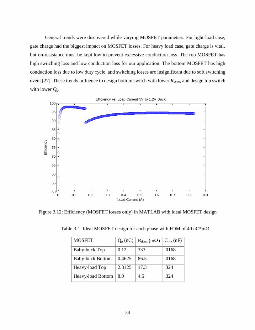
34
General trends were discovered while varying MOSFET parameters. For light-load case,
gate charge had the biggest impact on MOSFET losses. For heavy load case, gate charge is vital,
but on-resistance must be kept low to prevent excessive conduction loss. The top MOSFET has
high switching loss and low conduction loss for our application. The bottom MOSFET has high
conduction loss due to low duty cycle, and switching losses are insignificant due to soft switching
event [27]. These trends influence to design bottom switch with lower Rdson, and design top switch
with lower Qg.
Figure 3.12: Efficiency (MOSFET losses only) in MATLAB with ideal MOSFET design
Table 3-1: Ideal MOSFET design for each phase with FOM of 40 nC*m
MOSFET Qg (nC) Rdson (m) Coss (nF)
Baby-buck Top 0.12 333 .0168
Baby-buck Bottom 0.4625 86.5 .0168
Heavy-load Top 2.3125 17.3 .324
Heavy-load Bottom 8.0 4.5 .324
0 0.1 0.2 0.3 0.4 0.5 0.6 0.7 0.8 0.950
55
60
65
70
75
80
85
90
95
100
Load Current (A)
Eff
icie
ncy
Efficiency vs. Load Current 5V to 1.2V Buck

35
However, finding discrete parts with these parameters was not possible. Instead, MOSFETs
were selected with these trends. For the baby-buck phase, the smallest possible gate charge
MOSFETs were selected. Vishay’s MOSFET Si1012r were selected for the baby-buck phase due
to their low gate charge of 0.75 nC with disregard to high on-resistance of 500 m [28]Texas
Instrument’s MOSFET CSD15571Q2 were chosen for the heavy-load phase with gate charge of
2.5 nC and on-resistance of 16 m [29].
To demonstrate the effectiveness of these discrete MOSFET selections, a loss breakdown
is performed using simple loss equations 3.5 – 3.10. The baby-buck phase has a case of 60 mW
load with switching frequency of 100 kHz in DCM while the heavy-load phase has a case of 600
mW load with the switching frequency of 250kHz in CCM. In Figure 3.13, the two selected
MOSFETS for prototype are compared for the baby-buck phase. This demonstrates the importance
of low gate charge for the baby-buck phase. Si1012r (Case 1) has FOM of 375 nC*mwith total
loss of 2.35 mW compared to CSD15571Q2 (Case 2) with FOM of 40 nC*mand total loss of
9.87 mW. Even with substantially lower FOM and Rdson, TI’s MOSFET consumes more power.
Note, the conduction losses have little impact on the efficiency for the baby-buck phase, while
other losses dominate.
Figure 3.13: MOSFET loss breakdown of baby-buck phase with Case 1 – Si1012r and Case 2 –
CSD15571Q2
0
1
2
3
4
5
6
Pcond_BB Pgd_BB Pcoss_BB Psw_BB Pqrr_BB
Pow
er L
oss
(m
W)
MOSFET Loss Breakdown
Case 1
Case 2

36
In Figure 3.14, two selected MOSFETs with the same FOM (40 nC*m) are compared for
the heavy-load phase. This loss breakdown exhibits the importance of selecting proper MOSFETs
with appropriate gate charge and on-resistance for target load range. CSD13202Q2 (Case 2) has
Qg = 5.1 nC and Rdson = 8 mwith total loss of 121.8 mW compared to CSD15571Q2 (Case 1)
with Qg = 2.5 nC and Rdson = 16 mwith total loss of 68 mW. Even with the same FOM, MOSFET
device parameters have a huge impact on overall efficiency. Choosing CSD13202Q2 causes nearly
double the amount of loss compared to the selected MOSFET for prototype. Note, even with
heavier load, gate driving loss, switching loss, reverse recovery loss, and Coss loss can still
dominate the loss breakdown. To validate lower gate charge for heavy-load phase will not result
in higher efficiency, Si1012r was selected. Using Vishay’s MOSFET lead to 145 mW total loss,
with 125 mW stemming from conduction losses. This reiterates conduction losses become
significant for heavy loads.
Figure 3.14: MOSFET loss breakdown of heavy-load phase with Case 1 – CSD15571Q2 and
Case 2 – CSD13202Q2
To demonstrate the benefit of designing MOSFETs and integration, the designed
MOSFETs in Table 3-1 are compared to the discrete MOSFETs selected for prototype. Figure 3.15
shows the baby-buck phase with load power of 60 mW. The designed MOSFETs consume a total
0
10
20
30
40
50
60
70
80
90
100
Pcond_HL Pgd_HL Pcoss_HL Psw_HL Pqrr_HL
Pow
er L
oss
(m
W)
MOSFET Loss Breakdown
Case 1
Case 2

37
of 0.792 mW compared to 2.35 mW with discrete components. For the 60mW case, this would
result in a 3% efficiency improvement. Using the designed MOSFETs and integrating into IC
would boost very light load efficiency even further. Figure 3.16 shows the heavy-load phase with
load power of 600 mW. The designed MOSFETs consume a total of 66.3 mW compared to 68
mW with discrete components. For the specific load case, there is little benefit to have designed
MOSFETs with increase of efficiency by 0.3%. However, under heavier load, efficiency will
increase from reduction in conduction losses.
Figure 3.15: MOSFET loss breakdown of baby-buck phase, designed MOSFETS vs. selected
discrete parts
0
0.25
0.5
0.75
1
Pcond_BB Pgd_BB Pcoss_BB Psw_BB Pqrr_BB
Pow
er L
oss
(m
W)
MOSFET Loss Breakdown
Discrete Parts
Designed FETs

38
Figure 3.16: MOSFET loss breakdown of heavy-load phase, designed MOSFETS vs. selected
discrete parts
An open-loop prototype was designed and built to test the efficiency of the selected discrete
MOSFETs and determine the optimum transition point between the two phases, this is discussed
in more detail in Section 4.1.1.
3.4 Chapter Summary
The chapter describes design of a control scheme, phase selection control, and component
design for each phase of the proposed two-phase buck converter. It explains operation of the
individual COT control scheme for each phase, design of current sense block, design of phase
selection block, and a prototype with discrete components. Simulation results verify operation of
the phase selection and transition between the two phases during load step, which is the major
function. Optimization of each power stage demonstrates high efficiency for both phases with their
respective load range. Lastly, a MOSFET loss breakdown is performed to verify discrete MOSFET
selection and highlight benefits of designing through integration.
0
5
10
15
20
25
30
35
40
45
50
Pcond_HL Pgd_HL Pcoss_HL Psw_HL Pqrr_HL
Pow
er L
oss
(m
W)
MOSFET Loss Breakdown
Discrete Parts
Designed FETs

39
Chapter 4
Experimental Results
This chapter describes the design procedure for a prototype of the proposed two-phase buck
converter with discrete components. It includes an open-loop prototype with simulations and
efficiency measurements and two closed-loop prototypes with simulations and efficiency
measurements. Photos of the each prototype are given. The measurement setup and test procedure
for efficiency measurements are discussed. Next, simulation and measurement results for the phase
selection block due to load step are demonstrated. Efficiency and loss breakdown for the proposed
two-phase converter with optimum phase selection are presented. The measured transient
performance during phase transition is presented. Finally, future improvements for the proposed
two-phase converter are offered.
4.1 Prototype Design Procedure
The proposed two-phase buck converter with closed-loop control was implemented with
discrete components on a PCB. Several design steps were taken before the closed-loop prototype
was built. Various iterations of a prototype with discrete parts were designed and built to arrive at
the final design. Simulations were performed for each step to compare efficiency measurements,
and then ensure proper closed loop control.
4.1.1 Open-Loop Prototype and Simulations
The first step in the design process for a working prototype was to build an open-loop
prototype on a PCB to measure the efficiency of the power stage and compare to simulation results,
shown in Figure 4.1. An open-loop simulation of the power stage of each phase was performed in
OrCAD Capture. This simulation tool was used because of its ability to import encrypted models

40
of Texas Instruments’ MOSFETs. The simulation included models for MOSFETs, gate driver
LM5113, inductor DCR, capacitor ESR to properly model associated losses that would be present
on prototypes. PWM signals were used as inputs to the LM5113 so that dead time could be
adjusted. It is important to note that the simulations and the open-loop prototype are operating with
a constant switching frequency of 250 kHz and CCM for simplicity. PCB design and layout were
performed using Eagle and measurements taken with standard equipment.
Figure 4.1: Open-loop prototype of both phases with discrete components
The measurement setup to test the open-loop prototype efficiency involved one DC power
supply for Vin, one electronic load, two function generators to provide top and bottom gate signals,
and four digital multimeters to measure voltage and current at input and output. The test setup for
the final prototype converter measurements will be explained in detail in Section 4.2.

41
Figure 4.2: Open-loop baby-buck phase efficiency: prototype measurement vs. simulation
Figure 4.3: Open-loop heavy-load phase efficiency: prototype measurement vs. simulation
Figure 4.2 and Figure 4.3 are a comparison of the simulated efficiency using OrCAD
Capture and Pspice versus measured efficiency of the open-loop prototype. It can be seen that the
74%
76%
78%
80%
82%
84%
86%
88%
90%
30 300
Eff
icie
ncy
(%
)
Load (mW)
Measurement
Pspice
80.0%
82.5%
85.0%
87.5%
90.0%
92.5%
95.0%
97.5%
100.0%
100 1000
Eff
icie
ncy
(%
)
Load Power (mW)
Measurement
Pspice

42
simulated efficiency is higher than the measured efficiency for both phases across the entire load
range. There are several possible reasons for this discrepancy. First, the gate driver model
simulated losses are much lower than the measured losses, 1 mW compared to 5 mW for the baby-
buck phase and 4 mW compared to 10mW for heavy-load phase. Second, the loss under zero-load
for simulations is less than measured losses. This is because the simulations do not consider PCB
trace resistances and parasitic loop inductances. These parameters for each board cannot be
adequately measured with our equipment, so they cannot be quantified. For the baby-buck phase,
the no-load loss was simulated to be 2.8 mW compared to 4.7 mW and for the heavy-load phase,
simulated to be 7.2 mW compared to 24 mW. If the reasons for the discrepancy are taken into
account, the measured efficiency would match more closely to the simulated efficiency from
Pspice models.
Figure 4.4: Open-loop two-phase converter prototype efficiency
Measured efficiency data for each phase was collected and superimposed on one graph as
shown in Figure 4.4. This was performed to develop a general range for the load current in which
the transition between the two phases should occur. Illustrated in Figure 4.4, the optimum
transition point varies with input voltage, but remains in a relatively small range. Because of the
74.0%
76.0%
78.0%
80.0%
82.0%
84.0%
86.0%
88.0%
90.0%
20 200 2000
Eff
icie
ncy
(%
)
Load Power (mW)
Vin = 3.7V
Vin = 5V

43
proportional relationship between input voltage and ideal transition point, using the input voltage
to create the reference voltage, V(Iref), was implemented. Also, if the transition point is designed
to be fixed, a bandgap constant voltage can be used to create the reference voltage, V(Iref), instead.
4.1.2 Closed-Loop Prototype and Simulations
The next step in the design process is to implement the proposed control scheme into a
closed-loop prototype with discrete parts to verify operation. To ensure that the selected discrete
parts would function and optimum phase selection control could be obtained, simulations must be
performed first.
4.1.2.1 First Version
The first version of the closed loop prototype used controllers LTC3833, comparators
LT1720, and current sense IC LT1999-50 [17] [30] [31]. The first iteration of the closed-loop
prototype shown in Figure 4.5 had some minor issues. First, due to noise on the sensed load current
information signal, the output of the comparator would oscillate for a wide load range of about 50
mA. This would cause both phases to turn on and off rapidly for the 50mA load range, resulting
in lower efficiency. Second, the comparators and current sense IC selected consumed unnecessary
power in order to achieve high speed, 60 mW for propagation delay less than 50 ns. The extra
power consumption, lowered the overall efficiency, shown in Figure 4.6.
Figure 4.5: First version of closed-loop prototype with discrete components
44
Figure 4.6: Overall efficiency of closed-loop prototype, first version
4.1.2.2 Second Version
In order to fix the problems presented with the first closed-loop prototype, several aspects
of the design were changed. To prevent comparator oscillations near the transition threshold,
hysteresis was added to each comparator. By measuring the noise on the sensed load current
information and through empirical means, it was determined that a hysteresis of 30 mV would
alleviate this problem. A LTC1440 comparator was selected for its adjustable hysteresis up to 50
mV and its micro-power design. To reduce power consumption of the phase selection block, low
power ICs were selected at the expense of the speed in order to boost overall efficiency. Also, the
second version incorporated the means to measure the power consumption of each IC to perform
power loss breakdown analysis. To measure the power consumption of individual sub-blocks (such
as the comparators, the current sense IC, the logic gates, the controllers, and the gate drivers) of
the converter, all the sub-blocks were designed with either a jumper to measure current, or sense
resistor to measure voltage on their supply input.
Circuit level simulations of the designed control scheme using selected controller
(LTC3833), comparators (LTC1440), current sense IC (LT6105), and logic chips were performed
with LTspice. Ideal AND and OR gates, and different MOSFETs and gate drivers were used to
perform simulations due to lack of models from the part manufacturers. The purpose of the
simulations was to verify the designed control scheme in SIMPLIS using discrete parts for the
0%
10%
20%
30%
40%
50%
60%
70%
80%
90%
10 100 1000
Eff
icie
ncy
(%
)
Power (mW)

45
control loop and optimum phase selection. Since LTspice was the simulation tool, selected
MOSFETs, gate drivers, and logic gates could not be implemented due to their varying
manufacturer. Figure 4.7 shows the transition from baby-buck phase to heavy-load phase due to a
200mA load step and the return transition to light load.
Figure 4.7: LTspice simulation demonstrating transition between phases due to load steps
The top waveform is the current through the load, utilizing a 200 mA step-up and step-
down. The second plot, comparator inputs, represents the sensed load current information V(ILoad),
and the transition reference voltage, V(Iref). A transition delay of about 10 s exists due to
propagation delay of the comparator that hinders transient performance. The control signals for
each phase turn on the selected phase when high (5 V) and turn off the selected phase when low

46
(0V). In the third plot, V(a) represents the baby-buck control signal and V(b) represents the heavy-
load control signal. In the fourth plot, the inductor currents for the baby-buck phase L1 and heavy-
load phase L2 are shown to demonstrate the transition between phases such as Figure 3.9. Note
the designed overlap of 40 µs where both phases are on to reduce undershoot. Also, the inductor
current for the baby-buck phase under light load condition of 50 mA demonstrates the phase
operates in DCM with a lower switching frequency. The final waveform is the output voltage,
shown during both transitions, with an overshoot voltage and undershoot voltage less than 20 mV.
During load step-up, there exists two undershoot voltage occurrences – one from initial load step
and second from shutting down of baby-buck phase. From load step-down, a single instance
overshoot occurs from immediate transition. Simulations in LTspice proved the proper operation
of sensing load current, phase selection and transition, COT control loop design, and lowering of
switching frequency under very light load.
The second closed-loop prototype with discrete components is shown in Figure 4.8. The
three major sections of the prototype are highlighted in Figure 4.8. The baby-buck phase contains
the power stage and the associated control circuit, and is the same for the heavy-buck phase. The
phase selection block in the figure indicates the OPS (Optimal Phase Selection) control. Figure 4.9
shows the overall efficiency for the second version of the closed-loop prototype.
Figure 4.8: Second version of closed-loop prototype with discrete components

47
Figure 4.9: Overall efficiency of closed-loop prototype, second version
The blue shaded region highlights the load range in which the baby-buck phase is active
and the red shaded region for heavy-load phase. The efficiency of the baby-buck phase is about
52% at the load of 30mW and increases steadily as the load increases. The maximum efficiency
of the baby-buck phase is 79.5% its maximum load of 200mW. The efficiency of the heavy-load
phase achieves above 80% for its entire load range, with a maximum efficiency of 87%.
The controller and gate driver consume around 15 mW of quiescent power even when its
phase is shut down. The light-load efficiency suffers greatly from the heavy-load phase controller
and gate driver consuming power unnecessarily. If control can be added to shut down the opposing
phase’s controller and gate driver, efficiency can be improved. Also, the heavy-load efficiency can
be improved marginally through shutting down the baby-buck controller and gate driver. There is
a potential issue with adding this control, the transient performance during transition between the
30%
40%
50%
60%
70%
80%
90%
10 100 1000
Eff
icie
ncy
(%
)
Load Power (mW)
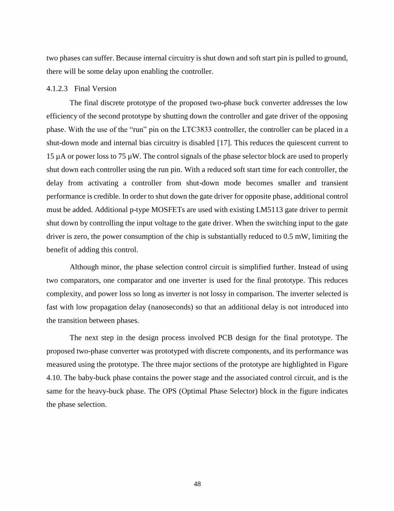
48
two phases can suffer. Because internal circuitry is shut down and soft start pin is pulled to ground,
there will be some delay upon enabling the controller.
4.1.2.3 Final Version
The final discrete prototype of the proposed two-phase buck converter addresses the low
efficiency of the second prototype by shutting down the controller and gate driver of the opposing
phase. With the use of the “run” pin on the LTC3833 controller, the controller can be placed in a
shut-down mode and internal bias circuitry is disabled [17]. This reduces the quiescent current to
15 µA or power loss to 75 µW. The control signals of the phase selector block are used to properly
shut down each controller using the run pin. With a reduced soft start time for each controller, the
delay from activating a controller from shut-down mode becomes smaller and transient
performance is credible. In order to shut down the gate driver for opposite phase, additional control
must be added. Additional p-type MOSFETs are used with existing LM5113 gate driver to permit
shut down by controlling the input voltage to the gate driver. When the switching input to the gate
driver is zero, the power consumption of the chip is substantially reduced to 0.5 mW, limiting the
benefit of adding this control.
Although minor, the phase selection control circuit is simplified further. Instead of using
two comparators, one comparator and one inverter is used for the final prototype. This reduces
complexity, and power loss so long as inverter is not lossy in comparison. The inverter selected is
fast with low propagation delay (nanoseconds) so that an additional delay is not introduced into
the transition between phases.
The next step in the design process involved PCB design for the final prototype. The
proposed two-phase converter was prototyped with discrete components, and its performance was
measured using the prototype. The three major sections of the prototype are highlighted in Figure
4.10. The baby-buck phase contains the power stage and the associated control circuit, and is the
same for the heavy-buck phase. The OPS (Optimal Phase Selector) block in the figure indicates
the phase selection.

49
Figure 4.10: Final closed-loop prototype with discrete components
4.2 Measurement Setup
The phase selection block was tested independently to validate proper control signals for
each phase based on associated load current. Both phases were installed and tested under steady
state conditions for various load currents using an electronic load. Switching signals D and D’ for
each phase were measured to confirm true phase selection resulting in shut down of opposite phase.
Switching signals were examined to verify constant frequency operation for the heavy-load phase
and reduced switching frequency under very light load for the baby-buck phase. The performance
of the two-phase converter was measured in terms of overall efficiency, power loss breakdown,
output voltage ripple, and output voltage under load transient.
The lowest supply voltage, at which the converter still could function correctly, was
observed as 4.35 V. This voltage droop was limited by the under voltage lockout (UVLO) of the
controller, LTC3833. Therefore, the proposed prototype converter cannot be operated using only
a Li-ion battery with maximum voltage of 4.2 V. A 5 V supply must be supplemented for the

50
prototype to function. For this reason, all measurements were performed using a 5 V supply to all
blocks.
Figure 4.11 shows the efficiency measurement test setup for the two-phase converter
prototype. A two-quadrant power supply (Hameg HM8143) is used as both the input power supply
and electronic load due to its ability to act as a current sink [32]. Several digital multimeters
(Agilent 34401A) are used to measure DC voltage and/or DC current for efficiency calculations
and power loss breakdown. A four-channel isolated oscilloscope (Tektronix TPS 2024B) observes
the switching and output voltage waveforms.

51
Figure 4.11: Test setup for efficiency measurements
Figure 4.12 shows the test setup for the two-phase converter under load-transient test. A
DC power supply (Agilent E3631A) is used as the 5 V input power supply. An electronic load
(Transistor Devices RBL488 100-120-800) with constant current pulse mode is utilized as a load
step [33]. A four-channel oscilloscope (Tektronix MSO5000) observes the output voltage, load
current, and the control signals for both baby-buck phase and heavy-load phase. A four-channel
isolated oscilloscope (Tektronix TPS 2024B) observes the inductor current waveforms of each
phase, VL1 and VL2, and the baby-buck control signal to trigger the transition event.
52
Figure 4.12: Test setup for load transient measurements
4.3 Measurement Results
Measurements in this section are divided into three sections: transient waveforms,
efficiency and loss breakdown, and load transient performance. First, transient waveform
measurements are taken under various loads to demonstrate proper phase selection in steady state,
varying of switching frequency, and output voltage. Second, efficiency measurements result in
overall efficiency of the prototyped two-phase converter. Power loss breakdown is measured at
two distinct states – one under light load and one under heavy load. Third, load transient
performance is measured to capture the transition between phases resulting from load step.
4.3.1 Transient Waveforms
4.3.1.1 Light Load
The light-load range for the proposed converter is the region, in which the baby-buck phase
is active, 30 mW to 200 mW. The baby-buck phase was designed to operate in CCM with a load
greater than 100 mW, while operating in DCM and lowering switching frequency under very light

53
load case less than 100 mW. The top gate voltages for three different load cases are shown in
Figures 4.13, 4.14, and 4.15. These figures demonstrate the reduction in switching frequency from
COT control with DCM.
Figure 4.13: Baby-buck top gate voltage with 150 mW load, CCM
Figure 4.13 shows the control MOSFET gate signals for each phase, baby-buck phase in
purple and heavy-load phase in green. With a load current of 125 mA or 150 mW, the baby-buck
phase will operate in CCM. The baby-buck phase is designed to operate in CCM with load current
of 100 mW to 200 mW when the heavy-load phase takes over. In CCM, the switching frequency
of the baby-buck phase is 248 kHz, while the heavy-load phase is inactive (not switching).
Figure 4.14: Baby-buck top gate voltage with 60 mW load, DCM
Figure 4.14 presents the control MOSFET gate signals for each phase, baby-buck phase in
purple and heavy-load phase in green, with load current of 50 mA or 60 mW. The baby-buck phase

54
is designed to operate in DCM with load current below 83 mA or 100 mW. This figure
demonstrates that the baby-buck phase is in fact in DCM. The portion of time, in which the gate
signal is zero, represents the synchronous MOSFET being on. When the control MOSFET is at
1.2 V, both MOSFETs are turned off and inductor current is zero. With a load of 60 mW, the
switching frequency reduces to 130.8 kHz, while the heavy-load phase is inactive.
Figure 4.15: Baby-buck top gate voltage with 30 mW load, DCM
Figure 4.15 displays the control MOSFET gate signals for each phase, baby-buck phase in
purple and heavy-load phase in green, with very light-load case of 25 mA or 30 mW load. The
baby-buck phase operates further in DCM, with a switching frequency reduced to 61.9 kHz, while
the heavy-load phase is shut down. The reduction in switching frequency helps boost efficiency
under light load.
The output voltage ripple under the lightest load, lowest switching frequency, must still
remain within specification of 30 mV. The output voltage ripple is measured with 30 mW load and
shown in Figure 4.16. The waveform is noisy, but its ripple voltage is observed to be about 28 mV.
As the lightest load is the worst case scenario due to low switching frequency, additional output
capacitance is not needed.

55
Figure 4.16: Output voltage ripple with 30 mW load, DCM
4.3.1.2 Heavy Load
The heavy-load range for the proposed converter is the region, in which the heavy-load
phase is active, 200 mW to 1 W. The heavy-load phase was designed to operate in CCM with a
load greater than 200 mW, meaning constant frequency operation for the specified load range.
Figure 4.17 shows the control MOSFET gate voltages for each phase for the load case of
240 mW. The gate voltage waveform demonstrates switching frequency near the phase transition
threshold. In CCM, the switching frequency of the heavy-load phase is 248 kHz. As the load
increases from 240 mW to max load, the switching frequency remains constant.
Figure 4.17: Heavy-load phase top gate voltage with 240 mW load, CCM

56
The output voltage ripple for any load within the heavy-load phase range remains constant.
This is because the phase operates in CCM, and the inductor current ripple remains constant
independent of output load current. Rather, the average inductor current varies proportionally to
load. The output voltage ripple must remain within the specification of 30 mV. The output voltage
ripple is measured with 240 mW load and shown in Figure 4.18. The waveform is noisy, but its
ripple voltage is observed to be at 20mV, additional output capacitance is not needed for the heavy-
load phase.
Figure 4.18: Output voltage ripple with 240 mW load, CCM
4.3.2 Efficiency and Loss Breakdown
The prototype of the two-phase converter was tested with 5 V input voltage provided from
a DC power supply, Hameg HM8143. The power supply outputs pass through a multimeter to
measure input current using the internal shunt resistor. For this reason, voltages are measured at
the board, not at the power supply, to ensure accuracy. An electronic load is used to vary the load
current using the Hameg HM8143 as a current sink. Input voltage is adjusted for various load
currents to keep input voltage at the board constant at 5 V. Overall efficiency was measured as
well as a power loss breakdown of each sub-block within closed loop control and phase selection.
4.3.2.1 Overall Efficiency
Recall, the baby-buck phase operates in the range from no load to 200 mW and the heavy-
load phase from 200 mW to 1 W. Overall efficiency was calculated from measured input voltage,

57
input current, output voltage, and output current using a single 5 V supply. Figure 4.19 shows
overall efficiency of the two-phase converter prototype. The blue shaded region highlights the load
range, in which the baby-buck phase is active and the red shaded region for heavy-load phase.
Figure 4.19: Overall Efficiency of the proposed two-phase converter final prototype
The efficiency of the baby-buck phase is about 64% at the load of 30 mW and increases
steadily as the load increases. The maximum efficiency of the baby-buck phase is 81% its
maximum load of 200 mW. The efficiency of the heavy-load phase achieves above 81% for its
entire load range, with a maximum efficiency of 88.2%. It is important to note, the overall
efficiency of the prototype converter is low at light load due to the power consumption of all blocks
and their respective integrated circuits. The power loss breakdown of each block and IC is covered
in the following section.
Figure 4.20 shows the efficiency of LTC3809, a comparable off-the-shelf converter
manufactured by Linear Technology. This converter has discrete MOSFETs, inductor, and output
capacitance. For the same power conversion of 5 V to 1.2 V, LTC3809 is more efficient for most
of the load range compared to the proposed converter prototype. Under light load of 60 mW, the
50%
55%
60%
65%
70%
75%
80%
85%
90%
10 100 1000
Eff
icie
ncy
Load Power (mW)

58
proposed converter achieves 64% efficiency, while LTC3809 achieves 83%. Under very light load,
the proposed converter is less efficient due to the power consumption of the discrete ICs used for
the controller. Under heavy load, the proposed converter is slightly more efficient from load range
of 400 mW to 700 mW. LTC3809 can achieve a higher efficiency at the maximum load for the
proposed design.
Figure 4.20: Efficiency of LTC3809 buck converter proposed by Linear Technology, “No
Rsense, Low EMI, Synchronous DC/DC Controller,” LTC3809 datasheet. [Online]. Available:
http://cds.linear.com/docs/en/datasheet/3809fc.pdf. [Accessed: 8-Dec-2014]. Used under fair use,
2014.
4.3.2.2 Power Loss Breakdown
Figure 4.21 shows the power loss breakdown of the proposed converter, it breaks down the
losses consumed by each IC in each block. The loss breakdown is performed at two load
conditions, one light-load case of 60 mW and one heavy-load case of 600 mW, with corresponding
efficiency of 71.7% and 87.8%. The loss breakdown indicates the major power loss is due to the
two controllers followed by the two gate drivers. Figure 4.22 shows the same power loss
breakdown in terms of percentage of total loss for each load case.
The baby-buck controller dissipates 8.6 mW (36.6%) under the light load of 60 mW, and

59
the gate driver dissipates 2.9 mW (12.3%). Therefore, the controller and the gate driver combined
consume 11.5 mW or 49% in total. Only the baby-buck phase controller and gate driver are active
for the light load, therefore the controller and gate driver of the heavy-load phase dissipate a total
of 0.056 mW (0.2%) under light load. The phase selector block includes load sense resistor, current
sense IC, comparators, and logic gates. Under light load of 60 mW, this block consumes total
power of 1.14 mW or 4.8%.
The heavy-load controller dissipates 9 mW (10.9%) under the heavy load of 600 mW, and
the gate driver dissipates 9.8 mW (11.9%). Therefore, the controller and the gate driver combined
consume 18.8 mW or 22.8% in total under the heavy load. The baby-buck phase is inactive, its
controller and gate driver dissipate a total of 0.056 mW (0.1%) under heavy load. Under heavy
load of 600 mW, the phase selector block has a total power loss of 8.44 mW or 10.2%. The phase
selector block consumes a higher percentage of total loss at heavy load due to the load sense
resistor and current sense IC.
Figure 4.21: Power loss breakdown of prototype two-phase converter: 60 mW and 600 mW load
0
2
4
6
8
10
12
Ctr
l. H
L
Ctr
l. B
B
Gat
e D
river
HL
Gat
e D
river
BB
Curr
ent
Sen
se
Load
Sen
se R
Log
ic G
ates
Com
par
ator
Pow
er L
oss
(m
W)
60 mW (50 mA)
600 mW (500 mA)

60
Figure 4.22: Percentage loss breakdown of prototype two-phase converter: 60 mW and 600 mW
load
4.3.3 Load Transient Performance
The transition between the two phases under load step was captured and presented in this
section. Load current step, control signals for each phase, output voltage, and inductor current
information during transition from step-up and step-down were recorded.
Measurements are taken using an electronic load with constant current pulse mode and
oscilloscopes to capture the transient waveforms. The load step under test is 25 mA (30 mW) to
225 mA (270 mW), or a 200 mA step-up and step-down. This load step incorporates the transition
between the two phases, with baby-buck in DCM at 25 mA and heavy-load phase active at 225
mA. The electronic load performs the 200 mA load step in 200 s, with a dI/dt rate of 2 A/ms. The
load current signal is measured using the current sample output signal of the Transistor Devices
electronic load [33]. The load current signal in blue has scale of 0.5 V/A. The control signals for
each phase indicate the control status from phase selection block, a high signal designates active
and low signal designates shutdown.
0.0%
5.0%
10.0%
15.0%
20.0%
25.0%
30.0%
35.0%
40.0%
Ctr
l. H
L
Ctr
l. B
B
Gat
e D
river
HL
Gat
e D
river
BB
Cu
rren
t S
ense
Load
Sen
se R
Logic
Gat
es
Com
par
ator
Pow
er L
oss
(%
)
60 mW (50 mA)
600 mW (500 mA)

61
The electronic load is set to perform a load transient with 150 Hz frequency and 50 % duty
cycle. In other words, each load step occurs at 75 Hz, or once every 13.33 ms. The output voltage
waveform remains within ripple specifications for both steady state operations. There are voltage
spikes upon transition between phases, these are examined in subsequent figures.
Figure 4.23: Load-transient performance from 200 mA load step down, output voltage (yellow),
load current (blue), baby-buck phase control signal (pink), and heavy-load phase control signal
(green)

62
Figure 4.24: Load-transient performance from 200 mA load step down, baby-buck phase control
signal (green), heavy-load phase inductor current (yellow), and baby-buck phase inductor current
(purple)
Figure 4.23 shows the overall load transient performance during a load step down, a
transition from heavy-load phase to baby-buck phase. As discussed in Section 4.1.2.2, the designed
immediate transition during load step-down yielded an undershoot voltage of around 20 mV using
LTspice for simulations. The baby-buck phase control signal goes high coinciding with the
transition of the heavy-load phase control signal going low. This incident is supported through
Figure 4.24, which displays the inductor current information for both phases. Initially, the heavy-
load phase inductor current (yellow) switches, while the baby-buck is shut down. Upon load step,
the baby-buck control signal goes high, all load current is immediately provided by the baby-buck
phase (purple), while heavy-load inductor current settles to zero. The output voltage during the
load step-down has an overshoot voltage of 10 mV. The overshoot voltage of the prototype is
within specification of 60 mV.

63
Figure 4.25: Load-transient performance from 200 mA load step up, output voltage (yellow),
load current (blue), baby-buck phase control signal (pink), and heavy-load phase control signal
(green)
Figure 4.26: Load-transient performance from 200 mA load step up, baby-buck phase control
signal (green), heavy-load phase inductor current (yellow), and baby-buck phase inductor current
(purple)

64
Figure 4.25 shows the overall load transient performance during load step up transition
from baby-buck phase to heavy-load phase. As discussed in Section 4.1.2.2, the designed overlap
of 40 µs during load step-up yielded an undershoot voltage of just under 20 mV in two instances
using LTspice for simulations. The baby-buck phase control signal remains high for around 60 µs
after the heavy-load phase control signal transitions to the high state. This event demonstrates the
overlap of both phases being active. This event is reinforced through Figure 4.26, which displays
the inductor current information for both phases. Initially, the baby-buck phase inductor current
(yellow) switches while heavy-load phase inductor current is zero. Second, the load current is
shared through the inductor in both phases. Finally, the baby-buck control signal goes low, and all
current is assumed by the heavy-load phase (purple).
The output voltage during load step-up actually has an overshoot voltage of 65 mV,
followed by an undershoot voltage of 10 mV. An overshoot occurs from the turning on of the
heavy-load phase, while the baby-buck phase has mostly assumed the load current. The reason for
this phenomenon is that the load step is too slow (200 µs). This allows the baby-buck control loop
to adequately increase its average inductor current at a similar rate to the load step. When the
heavy-load phase engages, an inrush current is provided to the load resulting in an overshoot
voltage. This was precisely the reason why an immediate transition is wanted for load step down,
discussed in Section 3.2.2. The overshoot voltage causes the transient performance of the prototype
to be slightly outside specification of 60 mV. The equipment provided for electronic load step
cannot perform a faster load step, therefore, these measurements are used to show the transition
between phases and functionality of OPS control.
4.4 Future Improvements
4.4.1 Discrete Prototype
In an attempt to increase heavy-load efficiency, an alternative method to sensing load
current could be used. The sense resistor and current sense IC that amplifies the differential voltage
consumes considerable power at very heavy load, (8.4 mW at 600 mW load). The inductor current
information from each phase is readily available as a voltage waveform. If the inductor current
information for each phase could be averaged and summed, a representation of load current could

65
be achieved. If this method were realized using less power than the current sense IC and its load
sense resistor, efficiency could be further improved, specifically at heavy load where sense resistor
loss becomes large.
4.4.2 Integration of Controller
The methods proposed above should be implemented into the integrated controller.
Designing of a simpler controller with less protection would also help increase overall efficiency
by reducing the quiescent current draw of the controller. Some additional design considerations
for integrating the controller are described. First, the current prototype has two gate drivers for
each phase, one integrated in the LTC3833 controller, and another independent to actually boost
the gate voltages and drive the top MOSFETs. Implementing only one gate driver circuit for each
phase will help reduce loss. Second, a low power comparator that has relatively fast transient
response (1 s compared to 12 s) will improve the transient performance by reducing propagation
delay, while maintaining the same efficiency. Third, the controller and subsequent blocks should
be designed to operate under lower input voltage, such as the 3.0 V minimum of a lithium ion
battery. Overall, design of the current sensing amplifier, logic AND gates, logic OR gates should
be performed with efficiency in mind.
Integration of MOSFETs would have a very high impact on very light-load efficiency.
Designing of the baby-buck phase MOSFETs to have ultra-low gate charge would minimize the
dominant switching losses and gate charge losses. Proper design of the synchronous MOSFETs
with lower Rdson for both phases would help minimize conduction losses to further increase heavy-
load efficiency for each phase. With integration and redesign of MOSFETs, a different optimal
load current transition point would occur.
4.5 Chapter Summary
The design procedure of the proposed two-phase buck converter prototype with discrete
components was discussed through all prototype iterations. Simulation results for the transition
between phases were shown. Steady-state measurement results of the final prototype indicate that
phase selection and shut off occur properly. Overall efficiency and loss breakdown for the

66
proposed two-phase converter with optimum phase selection was performed using the test setup
described. The efficiency / performance of the proposed two-phase buck converter cannot be
adequately compared to existing converters due to the use of off-the-shelf discrete ICs for our
prototype. The efficiency of the converter under light load of 30mW is 64% with a maximum
efficiency of 88% at 700 mW. The measured transient performance during phase transition was
presented and compared to the simulation results. The transient performance measurements
indicate proper functionality of OPS control design and transition. The measured transient
performance of the prototype was inferior to simulations, 10 mV overshoot during load step down
and 65 mV overshoot during load step up. Finally, future improvements for the proposed two-
phase converter with discrete components and integration was presented.

67
Conclusion
Power consumption of smart cameras varies significantly between sleep mode and active
mode, and a smart camera operates in sleep mode for 80 – 90% of time for typical use. To prolong
the battery life of smart cameras, it is essential to increase the power converter efficiency for light
load, while being able to manage heavy load. The power stage of traditional buck converter is
optimized for maximum load, at the cost of light-load efficiency. Wei proposed a multiphase buck
converter incorporating the baby-buck concept and optimum number of phases (ONP) control [4].
This thesis research investigated Wei’s multiphase buck converter to improve the light-load
efficiency for smart cameras as the target application.
Design of a two-phase buck converter and its control scheme using discrete components
was investigated in this thesis. The proposed two-phase buck converter aims to provide power for
microprocessors of smart cameras. The input voltage of the converter is 5 V DC, and the output
voltage is 1.2 V DC with power dissipation range of 25 mA (30 mW) for light load and 833 mA
(1 W) for heavy load. Three methods are considered to improve light-load efficiency: adopting
baby-buck concept, adapting ONP control for low-power range, and implementing a pulse
frequency modulation (PFM) control scheme with discontinuous conduction mode (DCM) to
lower switching frequency. The first method is to adopt the baby-buck concept through power
stage design of each phase to optimize efficiency for a specific load range. The baby-buck phase
is optimized for light load and the heavy-load phase is designed to handle the processors maximum
power consumption. The second method performs phase selection from sensed load current
information. Rather than have all phases active for heavy-load as in ONP control, optimum phase
selection (OPS) control is introduced to adaptively select between phases based on load current.
Due to low-power constraints, OPS is more efficient for the medium to heavy-load range. The
transition between phases due to load change is also investigated. The third and final method

68
implements PFM control with DCM to lower switching frequency and reduce switching and
driving losses under light load. PFM is accomplished with a constant on-time (COT) valley current
mode controller, which uses the inductor current information and output voltage to generate
switching signals for both the top and bottom switches. The baby-buck phase enters DCM to lower
switching frequency under very light load, while the heavy-load phase remains in continuous
conduction mode (CCM) throughout its load range.
The proposed two-phase converter prototype is realized using discrete components and
LTC3833 as the COT controller. Efficiency of the two-phase converter and a power loss
breakdown for each block in the control scheme were measured. The efficiency ranges from 64%
to 81% for light load ranging of 30 mW to 200 mW, and the efficiency ranges from 81% to 88%
for heavy load ranging from 200 mW to 1 W. The majority loss is due to controllers, which are
responsible for 37 % (8.6 mW) for light load of 60 mW and for 10.9 % (9 mW) for heavy load of
600 mW. The gate driver loss is considerable for heavy load of 600 mW, consuming 11.9%
(9.8mW). The converter has a 10 mV overshoot voltage for a load step-down from 225 mA to 25
mA, and it has 65 mV overshoot voltage for a load step-up from 25 mA to 225 mA. Although, a
fair comparison is difficult due to use of discrete parts for OPS control, the proposed converter
shows reasonably good efficiency and performance.
A few future research areas to improve the two-phase converter are suggested below.
Although superb load-transient performance is not a goal of the proposed converter, it can be
improved through design of load sensing circuit, comparator, and logic gates to be faster. This
must be done with power consumption in mind.
Discrete MOSFETS are a limitation of efficiency for this low power application. Design and
integration of MOSFETs would have a very high impact on light-load efficiency. Design of
the baby-buck phase MOSFETs to have ultra-low gate charge would minimize the dominant
switching losses and gate charge losses. Proper design of the synchronous MOSFETs for both
phases would help minimize conduction losses to further increase efficiency for heavy load.
The sense resistor and current sense IC consumes considerable power at very heavy load, (8.6
mW at 600 mW load). Further investigation into load sense methods could increase heavy-
load efficiency.

69
The above items are left for future research in two-phase converter design for low power
applications as well as integration into ICs.

70
References
[1] N. Mohan, T. M. Undeland, and W. P. Robbins, Power Electronics: Converters,
Applications, and Design, 3rd ed. New Jersey: John Wiley & Sons Inc., 2003.
[2] Q. Li. ECE 5254. Class Lecture, Topic: “Chapter 5: new current-mode control modeling
based on describing function method.” Bradley Dept. of Electrical and Computer
Engineering, Virginia Tech, Blacksburg, VA, Fall 2013.
[3] H. Nguyen, “Design, Analysis and Implementation of Multiphase Synchronous Buck DC-
DC Converter for Transportable Processor,” M.S. thesis, ECE, Virginia Tech, Blacksburg,
VA, 2004.
[4] J. Wei, “High Frequency, High Efficiency Voltage Regulators for Future
Microprocessors,” Ph.D. dissertation, ECE, Virginia Tech, Blacksburg, VA, 2004.
[5] M. Belloni, E. Bonizzoni, and F. Maloberti, “On the Design of Single-Inductor Multiple-
Output DC-DC Buck Converters,” International Symposium on Circuits and Systems
(ISCAS), 2008. IEEE International Symposium, May 2009, pp. 3049-3052.
[6] X. Zhou, M. Donati, L. Amoroso, and F. C. Lee, “Improved Light-Load Efficiency for Synchronous Rectifier Voltage Regulator Module,” IEEE Transactions on Power
Electronics, vol. 15, no. 5, pp. 826-834, Sept. 2000.
[7] V. G. Madhuravasal, “Extreme Temperature Switch Mode Power Supply based on Vee-
square Control Using Silicon Carbide, Silicon on Sapphire, Hybrid Technology.” Ph.D.
dissertation, ECE, Oklahoma State University, Stillwater, OK, 2009.
[8] J. Wang, J. Xu, and B. Bao, “Analysis of Pulse Bursting Phenomenon in Constant-On-
Time-Controlled Buck Converter,” IEEE Transactions on Industrial Electronics, vol. 58,
no. 12, pp. 5406-5410, Dec. 2011.
[9] P. Vivek, “Extending Efficiency in a DC/DC Converter with Automatic Mode Switching
from PFM to PWM.” M.S. thesis, ECEE, Arizona State University, Phoenix, AZ, May
2014.
[10] A. Raj, “Calculating Efficiency: PMP-DCDC Controllers,” Texas Instruments Appl.
Report SLVA390, Feb. 2010.
[11] J. Su, C. Hung, T. Chang, and C. Liu, “A novel phase shedding scheme for improved light-
load efficiency of Interleaved DC/DC converters,” Applied Power Electronics Conference
and Exposition (APEC), 2011. Twenty-Sixth Annual IEEE, pp. 1482-1487, March 2011.

71
[12] P. Zumel, C. Fernandez, A. de Castro, and O. Garcia, “Efficiency improvement in
multiphase converter by changing dynamically the number of phases,” Power Electronics
Specialists Conference, 2006. PESC ’06. 37th IEEE, pp. 18-22, June 2006.
[13] Texas Instruments, “3-V to 6-V input, 6-A output synchronous buck PWM switcher with
integrated FETs,” TPS546113 datasheet, [Online]. Available:
http://www.ti.com/lit/ds/symlink/tps54612.pdf. [Accessed: 27-Mar-2014].
[14] Y. Chen, D. Chen, Y, Lin, C. Chen, and C. Wang, “A novel constant on-time current-mode
control scheme to achieve adaptive voltage positioning for DC power converters,” IECON
2012 – 38th Annual Conference on IEEE Industrial Electronics Society, pp. 104-109, Oct.
2012.
[15] S. Gurram, O. Brennan, and T. Wilkerson, “DC-to-DC Switching-Regulator Insights –
Achieving Longer Battery Life in DSP Systems,” Analog Dialogue 41-12, [Online]
Available: http://www.analog.com/library/analogDialogue/archives/41-
12/switching_regulator.pdf. [Accessed: 15-Nov-2014].
[16] Linfinity, “A Simple Current-Sense Technique Eliminating a Sense Resistor,” Appl. Note
AN-7, July 1998.
[17] Linear Technology, “Fast Accurate Step-Down DC/DC Controller with Differential Output
Sensing,” LTC3833 datasheet, [Online]. Available:
http://cds.linear.com/docs/en/datasheet/3833f.pdf. [Accessed: 10-June-2014].
[18] Texas Instruments, “LM5113 5A, 100V Half-Bridge Gate Driver for Enhancement Mode
GaN FETs,” LM5113 datasheet, [Online]. Available:
http://www.ti.com/lit/ds/symlink/lm5113.pdf. [Accessed: 16-Feb-2014].
[19] Linear Technology, “Precision, Extended Input Range Current Sense Amplifier,” LT6105
datasheet. [Online]. Available: http://cds.linear.com/docs/en/datasheet/6105fa.pdf.
[Accessed: 15-Sept-2014].
[20] Linear Technology, “Ultralow Power Single/Dual Comparator with Reference,” LTC1440
datasheet. [Online]. Available: http://cds.linear.com/docs/en/datasheet/144012fd.pdf.
[Accessed: 14-Sept-2014].
[21] Linear Technology, LTPowerCAD II. V2.0, 2013 [Online]. Available
http://www.linear.com/solutions/1159. [Accessed: 10-Aug-2014].
[22] C. Cooper, “Electronic Design – Fundamentals buck-converter efficiency,” [Online].
Available: http://electronicdesign.com/power/fundamentals-buck-converter-efficiency.
[Accessed: 12-Jan-2014].

72
[23] R. W. Erickson and D. Maksimovic, Fundamentals of Power Electronics, 2nd ed. New
York: Springer Publishing, 2001.
[24] M. K. Kazimierczuk, RF Power Amplifiers, New Jersey: John Wiley and Sons Inc., 2014.
[25] Y. Ying, "Device Selection Criteria Based on Loss Modeling and Figure of Merit," M.S.
thesis, ECE, Virginia Tech, Blacksburg, VA, 2008.
[26] J. Klein, “Synchronous buck MOSFET loss calculations with Excel model,” Fairchild
Semiconductor Appl. Note AN-6005, Nov. 2014.
[27] J. Depew, “Efficiency Analysis of a Synchronous Buck Converter using Microsoft Office
Excel-Based Loss Calculator,” Microchip Technology Appl. Note AN1471, 2012.
[28] Vishay Siliconix, “N-Channel 1.8 V (G-S) MOSFET,” Si1012r datasheet. [Online].
Available: http://www.vishay.com/docs/71166/71166.pdf. [Accessed: 14-Jan-2014].
[29] Texas Instruments, “20-V N-Channel NexFET Power MOSFETs,” CSD15571Q2
datasheet. [Online]. Available: http://www.ti.com/lit/ds/symlink/csd15571q2.pdf.
[Accessed: 14-Jan-2014].
[30] Linear Technology, “Dual/Quad, 4.5ns, Single Supply 3V/5V Comparators with Rail-to-
Rail Outputs,” LT1720 datasheet. [Online]. Available:
http://cds.linear.com/docs/en/datasheet/17201fc.pdf . [Accessed: 20-Jun-2014].
[31] Linear Technology, “High Voltage, Bidirectional Current Sense Amplifier,” LT1999-50
datasheet. [Online]. Available: http://cds.linear.com/docs/en/datasheet/1999fb.pdf.
[Accessed: 22-Jun-2014].
[32] Hameg Instruments, “Arbitrary Power Supply HM8143,” HM8143 manual. [Online].
Available: http://www.testequipmentdepot.com/hameg/pdf/hm8143_manu.pdf.
[Accessed: 12-Nov-2014].
[33] Transistor Devices Inc., “Dynoload Electronic Load 800W,” RBL488 100-120-800
datasheet. [Online]. Available:
http://www.tdipower.com/PDF/dynaload/rbl_488_series_800w.pdf. [Accessed: 21-Nov-
2014].
[34] Linear Technology, “No Rsense, Low EMI, Synchronous DC/DC Controller,” LTC3809
datasheet. [Online]. Available: http://cds.linear.com/docs/en/datasheet/3809fc.pdf.
[Accessed: 8-Dec-2014].