Embed Size (px)
Citation preview
Dula Review
w
1
7
Si Millimeter -Wave IC Seen Through Si Wafer
December 1984 Volume 45 No. 4 RCARCI 45(4) 553-704 (1984)
0
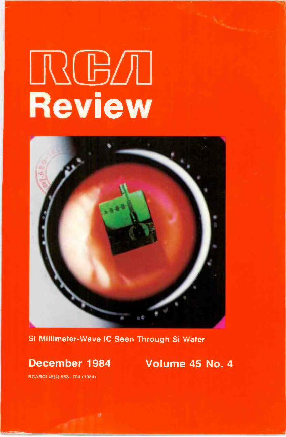
l Our cover shows a Silicon Millimeter - Wave Integrated Circuit (SIMMWIC) seen through a 1-2 µm thick Si wafer similar to that used to make the IC. The SIMMWIC technology, which includes high-energy ion implantation, pulsed laser annealing, and novel wafer thin- ning, is described in the paper by Sta- bile and Rosen in this issue of RCA Re- view.
RCA Review, published quarterly in March, June, September, and December by RCA Laboratories Princeton, New Jersey 08540. Entered as second class matter July 3, 1950 under the Act of March 3,
1879. Second-class postage paid at Princeton, New
Jersey, and at additional mailing offices. Effective January 1, 1983, subscription rates as follows: United States: one year 512.00, two years 521.00, three years $27.00; in other countries: one year 514.00, two years
524.50, three years $31.50. Single copies up to five years old 55.00
ncEal Review
Contents
555 Introduction M. Nowogrodzki and L. C. Upadhyayula
RCA Review (ISSN 0033-6831) is a technical journal published quarterly by RCA Laboratories
in cooperation with the subsidiaries and divisions
of RCA.
557 Advanced Applications and Solid -State Power Sources for Millimeter - Wave Systems Glenn R. Thoren
579 Millimeter -Wave Monolithic Passive Circuit Components S. C. Binari, R. E. Neidert, C. Kelner, and J. B. Boos
587 Silicon Technology for Millimeter -Wave Monolithic Circuits Paul J. Stabile and Arye Rosen
606 A GaAs Power FET Suitable for Monolithic Integration, with Laser - Processed Gate and Drain Via Connections R. L. Camisa. G. C. Taylor, F. P. Cuomo, W. F. Reichert, and R. Brown
619 Advances in Design of Solid -State Power Amplifiers for Satellite Communications B. R. Dornan, M. T. Cummings, and F. J. McGinty
631 Communication Receivers for Satellites-A Review H. B. Goldberg and S. S. Dhillon
651 A 14-GHz Cooled Low -Noise GaAs FET Amplifier for Communication Satellite Application G. R. Bi.sacca, P. A. Goldgeier, H. B. Goldberg, M. Noyes, and A. Chuchra
670 20-GHz Lumped -Element GaAs FET Driver Amplifier Shabbir S. Moochalla and Donald E. Aubert
681 Limiting Amplifier for Instantaneous Frequency Measuring System Robert E. Askew
688 Patents
692 Authors
701 Index, Vol. 45, 1984
December 1984 Volume 45 Number 4 ISSN 0033-6831
RCA Corporation Thornton F. Bradshaw Chairman and Chief Executive Officer Robert R. Frederick President and Chief Operating Officer
Editorial Advisory Board Chairman, K. H. Powers RCA Laboratories
J. K. Clemens RCA Laboratories G. C. Hennessy RCA Laboratories J. Kurshan RCA Laboratories B. J. Lechner RCA Laboratories R. D. Lohman RCA Laboratories W. J. Merz Laboratories RCA, Ltd. J. L. Miller RCA Laboratories A. Pinsky RCA Laboratories R. E. Quinn RCA Laboratories C. C. Richard International Licensing W. M. Webster RCA Laboratories B. F Williams RCA Laboratories
Editor Ralph F. Ciafone Assoc. Editor Eva Dukes
Editorial Representatives J. Dearing Broadcast Systems Division D. R. Higgs Missile and Surface Radar E. Janson Consumer Electronics Division M. Kaminsky RCA Service Company T. E. King Engineering E. Madenford Video Component and Display Division R. Mausler National Broadcasting Company M. G. Pietz Advanced Technology Laboratories C. T. Powell American Communications J. Schoen Solid State Division D. Wellinger Automated Systems D. Tannenbaum Government Communications Systems D. Unger Global Communications F. Yannotti Astro -Electronics
© RCA Corporation 1985. All rights reserved, except that express permission is hereby granted for the use in computer -based and other information -service sys- tems of titles and abstracts of papers published in RCA Review.
Introduction to Special Issue on Microwave Devices and Circuits In this special issue of RCA Review the reader will find some of the papers presented at the IEEE Princeton Section Sarnoff Symposium on Microwave and Millimeter -wave Devices and Circuits held at RCA Laboratories on March 24, 1984. This annual Symposium is
gaining popularity among researchers, both in the government and in industry, working in the area of advanced microwave technology, and has spurred the publication of special issues of the RCA Review devoted to the microwave art.
Reflecting current interest in the field, several of the papers de-
scribe advances in the practical utilization of millimeter -wave cir-
cuits and devices. Applications of power sources for millimeter -wave systems (Thoren) and the design of passive monolithic components (Binari et al.) are discussed, as is a new look at high -resistivity silicon for the construction of monolithic millimeter -wave circuits (Stabile and Rosen). R. Camisa et al. present an approach to mono-
lithic circuits in gallium arsenide ín which the usual tradeoff be-
tween thermal and electrical properties of the circuits is circum- vented. The remaining papers are devoted to components specifi- cally designed for satellite communications systems, another area where the microwave technology has been preeminent: communi- cations receivers (Goldberg and Dhillon), driver amplifiers (Moo -
challa and Aubert), and power amplifiers (Doman et al.) all use state-of-the-art GaAs FETs and hybrid circuit techniques.
M. Nowogrodzki and L. C. Upadhyayula Microwave Technology Center, RCA Laboratories, Princeton, NJ
RCA Review Vol. 45 December 1984 555

i
556 RCA Review Vol. 45 December 1984
Advanced Applications and Solid -State Power Sources for Millimeter -Wave Systems*
Glenn R. Thoren Raytheon Missile Systems Div., Hartwell Rd., Bedford, MA 01730
Abstract-Millimeter-Wave technology offers many advantages for com- munications and missile systems of the future. These benefits are presented with a discussion of their impact on millimeter - wave systems under development, including smart munitions, minimissiles, communications, fire control, and radiometry. Millimeter -wave solid-state power sources, in particular the IMPATT diode, have made lightweight integrated high -fre- quency systems a reality. The development of these power sources, including IMPATT power combining, is presented.
1. Introduction
Millimeter -wave technology has emerged from the laboratory into the forefront of systems development for the 1980s. Millimeter -wave frequencies were usually relegated to custom applications and pro- totype systems, principally for the military. That has changed. The military is now committed to use of millimeter waves in programs such as MILSTAR (Military Strategic Tactical and Relay) and MLRS (Multiple Launch Rocket System).1'2 Lockheed is funded to
develop the MILSTAR satellite network. It has been estimated that the component market for MILSTAR terminals alone could reach millions of dollars per year by 1990. MLRS will initiate a multiyear, multinational development program with many millions to be com-
Part of this paper is a revised version of a paper published in the Microwave Systems News (MSN) in September 1983, p. 109. This paper was presented at an
IEEE Princeton Section symposium on "Microwave and Millimeter -Wave Solid - State Devices and Circuits" held at RCA Laboratories, Princeton, NJ on March 24,
1984.
RCA Review Vol. 45 December 1984 557
mitted to developing an autonomous minimissile, called the "ter- minally guided submunition", containing its own active millimeter - wave seeker. Commercial applications for secure communications links and satellite -to -satellite data links are also emerging. These commitments by government and industry have initiated a new era in the development of millimeter -wave systems. One of the prime technological thresholds crossed in reaching this new status was the advent of the solid-state transmitter using Gunn diodes, IMPATT diodes, or both.
In this paper we first discuss the status of millimeter -wave system development and then describe solid-state power sources for use with these systems.
2. Advantages of Millimeter Waves
Millimeter waves offer many advantages over microwave or in- frared systems. A few key features are:
Lightweight Small Size Broad Bandwidths (several GHz) Operation in Adverse Weather (cuts through fog, haze, smoke, dust, and debris) Narrow Beamwidths with High Resolution, Resistance to Jam- ming, and Low Probability of Intercept Covert Capability of 60 GHz May "See" Stealthy Targets (absorbers at 10 GHz reflect at 100 GHz) These features are exploited in a large array of systems appli-
cations beside the MILSTAR and MLRS program, e.g., radio As- tronomy has been using higher frequency equipment for many years. Other special applications include clear -air turbulence de- tectors, weather radars, nuclear spectroscopy, missile guidance, fuzes, motion detectors, map -matching radars, plume detection, and air -traffic -control beacons. However, the use of millimeter waves in systems that required large production runs awaited the arrival of a solid-state power source and a more mature component technology for all the high -frequency parts. The inherent advantages of small size, high reliability, and lightweight could only be realized in the total system when the millimeter -wave power source was also small, low voltage, reliable, and obviously lightweight. With the development of the IMPATT diode, made from silicon or gallium arsenide, and the Gunn diode, made from gallium arsenide or in- dium phosphide, suitable power sources became available with a
558 RCA Review Vol. 45 December 1984
MILLIMETER -WAVE SYSTEMS
sufficiently high confidence level to permit the development of major systems.
Of equal importance in the quest for millimeter -wave capability is an understanding of the device physics and the availability of instrumentation to measure and evaluate the various system com- ponents. An example is the wealth of information that can be ob-
tained from an automatic network analyzer at millimeter -wave fre-
quencies. As circuits get smaller (proportional to the smaller wave- lengths), it becomes more difficult to predict their behavior based on simple circuit models. Diode packages and even imprecise ma- chining of the component housing can yield large reactive and re-
sistive parasitics that drastically affect the performance of a com-
ponent. Clever use of the network analyzer can isolate these prob- lems, aid in circuit design for broadband performance, and confirm theoretical predictions of solid-state physics for power sources such as the IMPATT diodes.
Only very recently has capable instrumentation become available to exploit accurate component design techniques. It is difficult to envision large production runs of millimeter -wave components without first understanding the physics of the design and carefully accumulating the measurement data to validate the circuit design. The device physics, most notably for GaAs IMPATTS above 40 GHz, have only recently been explained. Above 100 GHz, the instrumen- tation for accurate network analysis is not available.
3. The Millimeter -Wave Spectrum
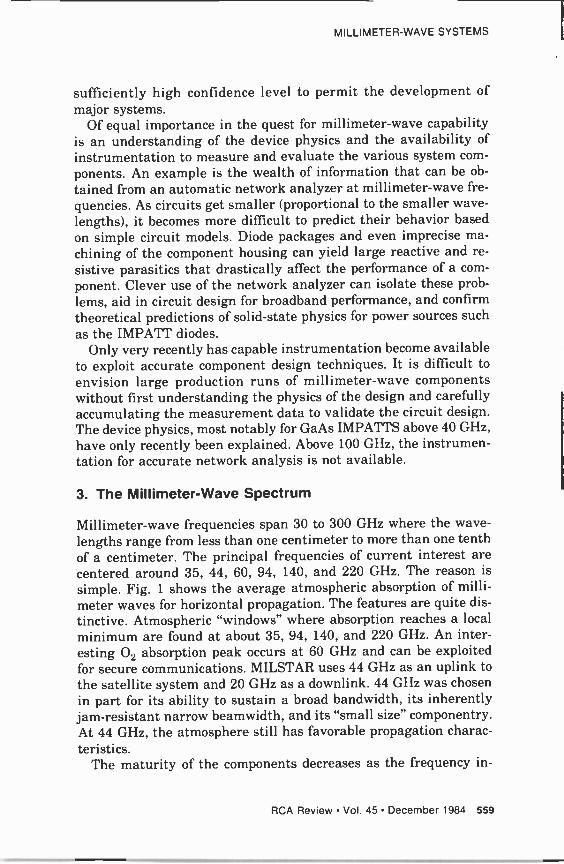
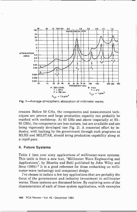
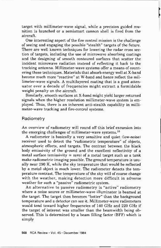
Millimeter -wave frequencies span 30 to 300 GHz where the wave- lengths range from less than one centimeter to more than one tenth of a centimeter. The principal frequencies of current interest are centered around 35, 44, 60, 94, 140, and 220 GHz. The reason is
simple. Fig. 1 shows the average atmospheric absorption of milli- meter waves for horizontal propagation. The features are quite dis- tinctive. Atmospheric "windows" where absorption reaches a local minimum are found at about 35, 94, 140, and 220 GHz. An inter- esting 02 absorption peak occurs at 60 GHz and can be exploited for secure communications. MILSTAR uses 44 GHz as an uplink to the satellite system and 20 GHz as a downlink. 44 GHz was chosen in part for its ability to sustain a broad bandwidth, its inherently jam -resistant narrow beamwidth, and its "small size" componentry. At 44 GHz, the atmosphere still has favorable propagation charac- teristics.
The maturity of the components decreases as the frequency in -
RCA Review Vol. 45 December 1984 559
100
40
20
10
2
1
ATTENUATION dB/km 0.4
0.2
0.1
0.04
0.02
0.004
0.002
0.001 10
30 20 15 10.0 8 0 6.0 4.0 3 0 2 0 1.5 1.0
WAVELENGTH (mm)
A
B H20
02 f
02
H20 H20-
15 20 25 30 40 50 60 70 80
FREQUENCY GHz A: SEA LEVEL
T = 20°C P = 760 mm
PH = 7.5 grlm3
Fig. 1-Average atmospheric absorption of millimeter waves.
100 150
B: 4 km T = 0°C
PH = 1 grlm3
250 300 400
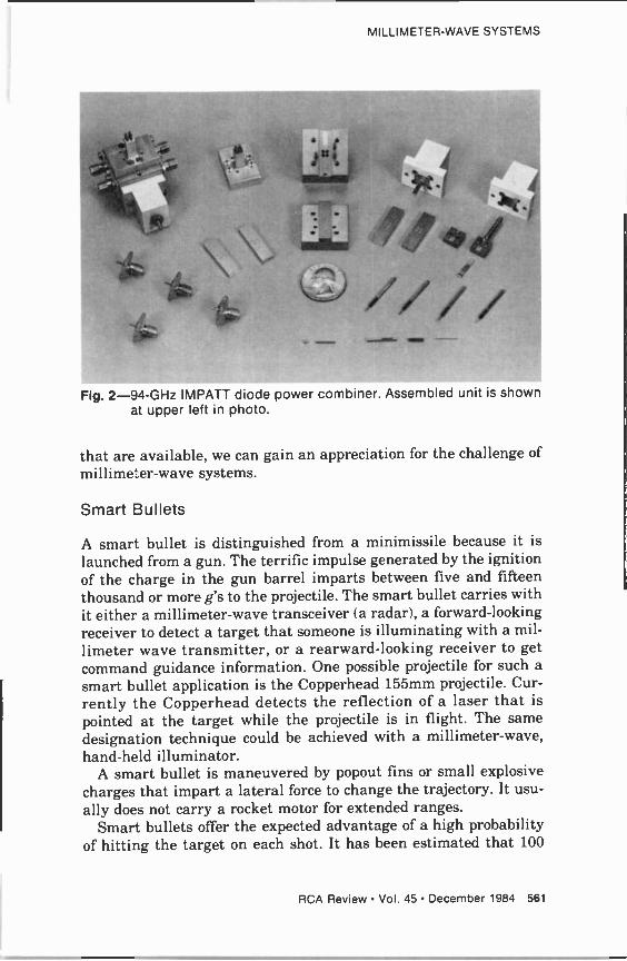
creases. Below 50 GHz, the components and measurement tech- niques are proven and large production capacity can probably be reached with confidence. At 60 GHz and above (especially at 93- 95 GHz), the components are less mature, but are available and are being vigorously developed (see Fig. 2). A concerted effort by in- dustry, with backing by the government through such programs as MLRS and MILSTAR, should bring production capability along at a rapid pace.
4. Future Systems
Table 1 lists over sixty applications of millimeter -wave systems. This table is from a new text, "Millimeter Wave Engineering and Applications", by Bhartia and Bahl published by John Wiley and Sons (1984).3 It is a good reference for those embarking on milli- meter -wave technology and component design.
I've chosen to isolate a few key applications that are probably the focus of the government and industry investment in millimeter waves. These systems are discussed below. By exploring some of the characteristics of each of these system applications, with examples
560 RCA Review Vol. 45 December 1984
MILLIMETER -WAVE SYSTEMS
*; =..
r.'
Fig. 2-94-GHz IMPATT diode power combiner. Assembled unit is shown at upper left in photo.
that are available, we can gain an appreciation for the challenge of millimeter -wave systems.
Smart Bullets
A smart bullet is distinguished from a minimissile because it is
launched from a gun. The terrific impulse generated by the ignition of the charge in the gun barrel imparts between five and fifteen thousand or more g's to the projectile. The smart bullet carries with it either a millimeter -wave transceiver (a radar), a forward -looking receiver to detect a target that someone is illuminating with a mil-
limeter wave transmitter, or a rearward -looking receiver to get command guidance information. One possible projectile for such a
smart bullet application is the Copperhead 155mm projectile. Cur- rently the Copperhead detects the reflection of a laser that is pointed at the target while the projectile is ín flight. The same designation technique could be achieved with a millimeter -wave, hand-held illuminator.
A smart bullet is maneuvered by popout fins or small explosive charges that impart a lateral force to change the trajectory. It usu- ally does not carry a rocket motor for extended ranges.
Smart bullets offer the expected advantage of a high probability of hitting the target on each shot. It has been estimated that 100
RCA Review Vol. 45 December 1984 561
Table 1-Millimeter-Wave Applications
Radar
Low angle tracking Secure military radar Interference free radar Cloud sensing radar High resolution radar Imaging radar Ground mapping Map matching Space object identification Lunar radar astronomy Target characteristics Weather radar Clear -air turbulence sensor Target designators Range finders Detection/classification of
ground vehicles LPI radar Radar cross-section measurements
Remote sensing of the environment Surveillance Target acquisition Missile guidance Navigation Obstacle detection Clutter suppression Fuses Harbor surveillance radar Airport surface detection radar Landing aids Air traffic control beacons Jet engine exhaust and cannon blast Beam riders Passive seekers Imaging Hand-held radar Active missile seekers
(terminal guidance)
Communications
Secure military communications Point to point extremely wideband
communications Spacecraft communications during
blackout Interference free communications
Satellite to satellite communications Inter satellite relays Earth to space communications Retroreflector communications LPJ communications Railroad communications
Radiometry
Remote sensing of the environment Radio astronomy Radio sextant Ship detection Space -based radiometers
Ground target detection Missile detection Missile guidance Clear -air turbulence sensor
Instrumentation
Plasma diagnostics Rocket exhaust plume measurements Remote vibration sensor Model radar cross-section
measurements
Automatic braking Spectroscopy Prediction of blast focusing Classroom demonstration
of optics
to 200 randomly placed "dumb" rounds bombarding a target area are needed before one effectively hits a target. The logistics of car- rying that many shells imposes a serious burden on front line forces. The smart bullet offers an effective alternative.
Minimissiles and Missiles A more sophisticated approach to the intelligent munition is the minimissile. Hughes Aircraft has conducted extensive tests on a
562 RCA Review Vol. 45 December 1984
MILLIMETER -WAVE SYSTEMS
millimeter -wave minimissile developed for the Air Force called WASP (wide -area smart projectile). The feasibility of such a missile with a pulsed 94-GHz active seeker radar has been proven. Targets were acquired and a tank was hit as the WASP glided in on the returning radar signature. The WASP missile was intended for a
multimissile pod dispenser placed under the wing of an aircraft. Unfortunately the cost per round of this advanced system was too
high and development was concluded. The Army is sponsoring an excítíng new program called MLRS
in cooperation with development partners Great Britain, France, Italy, and the Netherlands. The Multiple Launch Rocket System (MLRS) is a tracked vehicle that contains two "six packs" of missile launchers (12 missiles overall). To make these battlefield missiles more effective, six new millimeter -wave minimissiles will be con-
tained within each main missile. At a predetermined time, each main missile will eject the six terminally guided submissiles (TGSM's) which will glide over the target area and look down with
their millimeter -wave radar for targets. Each minimissile has a
high probability of finding a target in a "target -rich" environment and will swoop in for a near -vertical hit on the less armored topside of the tank. Sophisticated signal processing will eventually enable the missile to categorize and classify each target by its radar return as a tank, truck, or artillery piece.
Modifications of such minimissiles can be envisioned for air-to- air, air -to -ground, and ground -to -air applications as well. The ability to see stealthy targets may be an advantage for millimeter - wave minimissiles. Absorbers at X -band are often highly reflective at W -band. "Smooth" contours at lower frequencies can look more
pronounced at W -band as the radar resolution increases. So missiles used against low -cross-section cruise missiles or stealth -like aircraft may be suitable for millimeter waves. Because of the economy of
size and weight in high -frequency systems, a dual -mode IR MMW
or 35-GHz/94-GHz radar can be considered. Each of these dual -mode
approaches exploits the ability of millimeter -wave radar to see
through fog, dust, clouds, smoke, and debris, environments in which
infrared and optical guidance systems will not operate. As mentioned earlier millimeter -wave radars are also hard to
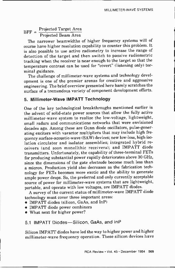
jam. First you have to find the missile, and then you need to point the jammer at the missile. This also assumes each target has the
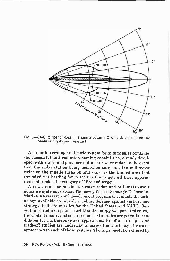
state-of-the-art componentry required to constitute a millimeter - wave jammer. Fig. 3 illustrates the narrow beam projected at mil-
limeter -wave frequencies; 94-GHz beams can be two degrees or less
in heamwidth.
RCA Review Vol. 45 December 1984 563
30°
20°
10°
10°
7 pF O
rFC 7./0
4C F''/
30° o
20°
Fig. 3-94-GHz "pencil -beam" antenna pattern. Obviously, such a narrow beam is highly jam resistant.
Another interesting dual -mode system for minimissiles combines the successful anti -radiation homing capabilities, already devel- oped, with a terminal guidance millimeter -wave radar. In the event that the radar station being homed on turns off, the millimeter radar on the missile turns on and searches the limited area that the missile is heading for to acquire the target. All these applica- tions fall under the category of "fire and forget".
A new arena for millimeter -wave radar and millimeter -wave guidance systems is space. The newly formed Strategic Defense In- itiative is a research and development program to evaluate the tech- nology available to provide a robust defense against tactical and strategic ballistic missiles for the United States and NATO. Sur- veillance radars, space -based kinetic energy weapons (missiles), fire -control radars, and surface -launched missiles are potential can- didates for millimeter -wave approaches. Proof of principle and trade-off studies are underway to assess the capability of various approaches to each of these systems. The high resolution offered by
564 RCA Review Vol. 45 December 1984
MILLIMETER -WAVE SYSTEMS
millimeter -wave systems, even at ranges of a thousand kilometers or more, may provide significant advantages, especially in isolating real targets from decoys.
Communications
Taking advantage of the lighter weight, broad -bandwidth capa- bility, small size, and especially the low probability of intercept, satellite communications networks have become a dynamic market for millimeter -waves. Uplinks at 30 and 44 GHz are being made for commercial and MILSTAR applications.
Downlinks at 20 GHz are also being developed for these systems. Satellite crosslinks for secure communications are being developed at 60 GHz. The high absorption peak at 60 GHz makes either jam- ming or eavesdropping from the ground virtually impossible. The narrow beamwidths also assure communication links that can't be easily intercepted even in space. Very high data rates can be trans- mitted over channels with more than a couple of GHz of bandwidth. Also, many channels can be provided.
A close look at the scope of the MILSTAR program will provide a sense of the commitment and the development effort that is spur- ring a large investment in millimeter -wave development by in- dustry.
MILSTAR is scheduled to be in place as a nuclear survivable communications network in the 1990's. There will be four satellites in geosynchronous orbit with three more in polar orbits. It is ex- pected that more than 4,000 strategic and tactical MILSTAR ter- minals will be placed on ships, aircraft, ground equipment, and submarines. The Army, Navy, and Air Force are each supporting program development efforts. The overall system integration is being run by the Air Force Space Division.
In 1986-87 the Navy program NESP (Navy EHF Satellite Pro- gram) will test six EHF terminals. Three will be ship mounted, two on submarines, and one land based. An attachment (called an EHF applique) to the FLTSATCOM satellite will be the spaceborne link. Raytheon and Harris are funded to develop these terminals for de- livery in 1986. Both companies have shown substantial progress. Raytheon is developing solid state transmitters and a TWTA ca- pable of more than 200 watts. Typical NESP antennas being de- veloped by Harris include a 2 -ft shipboard dish, a 5 -ft ground based dish, and a 3 -inch periscope -mounted design. The Navy is seeking 400 MILSTAR terminals in their initial acquisition.
The Air Force Electronic Systems Division has contracted with
RCA Review Vol. 45 December 1984 565
two teams to develop terminals for B52's, B1B's, E3A's AWACS, and E4 aircraft. The teams of Raytheon/Rockwell and Hughes/MA- COM each have $40 million to develop the prototype airborne ter- minals in the first phase of this development. The second phase winner will be required to build 20 to 25 terminals over two years for about $200 million. Advanced technologies such as VHSIC and GaAs monolithic microwave modules will likely be used in this ef- fort especially for the 20-GHz receive array. Monolithic GaAs cir- cuits above 30 GHz are at the cutting edge of the state of the art and require further development.
The space segment under the supervision of Lockheed will of course need 44-GHz receiving networks. Hughes Space and Com- munications Group is supplying the EHF component expertise for the 44-GHz receive and 20-GHz transmit portions of the satellite.
As can been seen, the depth and breadth of the MILSTAR pro- gram represents a serious and exciting business opportunity and the major motivation for rapid development of 44-GHz technology and systems.
On the ground (within the atmosphere), 60 GHz offers a unique approach to secure communications. Since 60 GHz is rapidly atten- uated by the 02 absorption in the atmosphere, the antenna sidelobes of a "secure" link are nearly impossible to pick up. If the transmitter and receiver are tuned for optimum performance in the secure mode (i.e., receiver at maximum sensitivity with transmitter at minimum necessary power levels), then any receiver (or detector) that might be present beyond the line -of -sight receiving station will have a difficult time receiving the signal. The narrow beamwidths add even greater resistance to interception to this secure, station -to - station system.
Fire Control
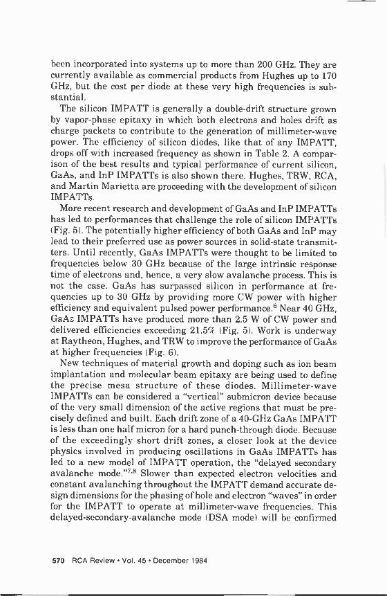
Millimeter -wave systems are exceedingly well suited for fire con- trol. It may be difficult, however, to scan the entire sky with the narrow millimeter -wave beams, though there are some "fan beam" designs that can accomplish this. Let us assume that a smaller search volume has been isolated by IR or lower -frequency radar. Now the beamwidths of millimeter -wave radars can be used to de- cided advantage. The Advanced Fire Control Radar (AFCORS) pro- gram at Raytheon showed that the narrow beamwidths at W -band could lock -on and track an aircraft target right down to the treetops. The low altitude clutter environment had little or no effect on the radar; conversely, X -band and Ka -band radars may have difficulty
566 RCA Review Vol. 45 December 1984
MILLIMETER -WAVE SYSTEMS
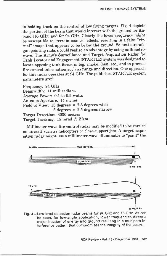
in holding track on the control of low flying targets. Fig. 4 depicts the portion of the beam that would interact with the ground for Ka -
band (16 GHz) and for 94 GHz. Clearly the lower frequency might be susceptible to "terrain -bounce" effects, resulting in a false "vir-
tual" image that appears to be below the ground. So anti -aircraft - gun poíntíng radars could realize an advantage by using millimeter - wave. The Army's Surveillance and Target Acquisition Radar for
Tank Locator and Engagement (STARTLE) system was designed to
locate opposing tank forces in fog, smoke, dust, etc., and to provide fire control information such as range and direction. One approach for this radar operates at 94 GHz. The published STARTLE system parameters are:4
Frequency: 94 GHz Beamwidth: 11 milliradians Average Power: 0.1 to 0.5 watts Antenna Aperture: 14 inches Field of View: 15 degrees x 7.5 degrees wide
5 degrees x 2.5 degrees narrow Target Detection: 3000 meters Target Tracking: 15 mrad a 2 km
Millimeter -wave fire control radar may be modified to be carried on aircraft such as helicopters or close -support jets. A target acqui- sition radar might use a millimeter -wave illuminator to "paint" the
94 GHz 3000 METERS
SURFACE 18 METERS
90 METERS
Fig. 4-Low-level detection radar beams for 94 GHz and 16 GHz. As can
be seen, for low -angle application, lower frequencies direct a
major fraction of energy into ground resulting in a multipath in- terference pattern that compromises the integrity of the beam.
RCA Review Vol. 45 December 1984 567
target with millimeter -wave signal, while a precision guided mu- nition is launched or a semismart cannon shell is fired from the aircraft.
One interesting aspect of the fire control mission is the challenge of seeing and engaging the possible "stealth" targets of the future. There are well known techniques for lowering the radar cross sec- tion of targets, including the use of microwave absorbing coatings and the designing of smooth contoured surfaces that scatter the incident microwave radiation instead of reflecting it back to the tracking antenna. Millimeter -wave systems offer a means of count- ering these techniques. Materials that absorb energy well at X -band become much more "reactive" at W -band and hence reflect the mil- limeter -wave signals. A multilayered coating that is a good atten- uator over a decade of frequencies might extract a formidable weight penalty on the aircraft.
Similarly, smooth surfaces at X -band might yield larger returned signals when the higher resolution millimeter -wave system is em- ployed. Thus, there is an inherent anti -stealth capability in milli- meter -wave tracking and fire -control systems.
Radiometry
An overview of radiometry will round off this brief excursion into the emerging challenges of millimeter -wave systems.'°
A radiometer is basically a very sensitive and quiet (low -noise) receiver used to detect the "radiometric temperature" of objects, atmospheric effects, and targets. The contrast between the black body emissivity of the ground and the excellent reflectivity of a metal surface (emissivity - zero) of a metal target such as a tank make radiometric imaging possible. The ground temperature is usu- ally near 290 K, while the sky temperature that would be reflected by a metal object is much lower. The radiometer detects the tem- perature contrast. The temperature of the sky will of course change with the weather, making detection more difficult in adverse weather for such a "passive" radiometric system.
An alternative to passive radiometry is "active" radiometry where a noise source or millimeter -wave illuminator is beamed at the target. The target then becomes "hotter" than the background temperature and a detector can see it. Millimeter -wave radiometers would tend toward higher frequencies of 140 GHz and 220 GHz if the target of interest was smaller than the beamwidth being ob- served. This is determined by a beam filling factor (BFF) which is simply
568 RCA Review Vol. 45 December 1984
MILLIMETER -WAVE SYSTEMS
Projected Target Area BFF =
Projected Beam Area The narrower beamwidths of higher frequency systems will of
course have higher resolution capability to counter this problem. It is also possible to use active radiometry to increase the range of
detection of the target and then switch to passive radiometric tracking when the receiver is near enough to the target so that the temperature contrast can be used for "covert" (listening only) ter- minal guidance.
The challenge of millimeter -wave systems and technology devel- opment is one of the premier arenas for creative and aggressive engineering. The brief overview presented here barely scratches the surface of a tremendous variety of component development efforts.
5. Millimeter -Wave IMPATT Technology
One of the key technological breakthroughs mentioned earlier is
the advent of solid-state power sources that allow the fully active millimeter -wave system to realize the low -voltage, lightweight, small radars and communications networks that were envisioned decades ago. Among these are Gunn diode oscillators, pulse -gener- ating exciters with varactor multipliers that may include high fre-
quency surface -acoustic -wave (SAW) devices; new low -loss, high iso-
lation circulator and isolator assemblies; integrated hybrid re- ceivers (and soon monolithic receivers); and IMPATT diode transmitters. Unfortunately, the capability of three -terminal FETs for producing substantial power rapidly deteriorates above 30 GHz,
since the dimensions of the gate electrode become much less than a micron. Production yield also decreases as the fabrication tech- nology for FETs becomes more exotic and the ability to generate ample power drops. So, the preferred and only currently acceptable source of power for millimeter -wave systems that are lightweight, portable, and operate with low voltages, are IMPATT diodes.
A survey of the current status of millimeter -wave IMPATT diode technology must cover three important areas:
IMPATT diodes (silicon, GaAs, and InP) IMPATT diode power combiners What next for higher power?
5.1 IMPATT Diodes-Silicon, GaAs, and InP
Silicon IMPATT diodes have led the way to higher power and higher millimeter -wave frequency operation. These silicon devices have
RCA Review Vol. 45 December 1984 569
been incorporated into systems up to more than 200 GHz. They are currently available as commercial products from Hughes up to 170 GHz, but the cost per diode at these very high frequencies is sub- stantial.
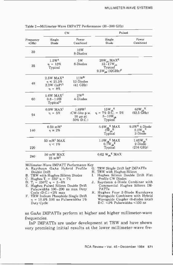
The silicon IMPATT is generally a double -drift structure grown by vapor -phase epitaxy in which both electrons and holes drift as charge packets to contribute to the generation of millimeter -wave power. The efficiency of silicon diodes, like that of any IMPATT, drops off with increased frequency as shown in Table 2. A compar- ison of the best results and typical performance of current silicon, GaAs, and InP IMPATTs is also shown there. Hughes, TRW, RCA, and Martin Marietta are proceeding with the development of silicon IMPATTs.
More recent research and development of GaAs and InP IMPATTs has led to performances that challenge the role of silicon IMPATTs (Fig. 5). The potentially higher efficiency of both GaAs and InP may lead to their preferred use as power sources in solid-state transmit- ters. Until recently, GaAs IMPATTs were thought to be limited to frequencies below 30 GHz because of the lai ge intrinsic response time of electrons and, hence, a very slow avalanche process. This is not the case. GaAs has surpassed silicon in performance at fre- quencies up to 30 GHz by providing more CW power with higher efficiency and equivalent pulsed power performances Near 40 GHz, GaAs IMPATTs have produced more than 2.5 W of CW power and delivered efficiencies exceeding 21.5% (Fig. 5). Work is underway at Raytheon, Hughes, and TRW to improve the performance of GaAs at higher frequencies (Fig. 6).
New techniques of material growth and doping such as ion beam implantation and molecular beam epitaxy are being used to define the precise mesa structure of these diodes. Millimeter -wave IMPATTs can be considered a "vertical" submicron device because of the very small dimension of the active regions that must be pre- cisely defined and built. Each drift zone of a 40-GHz GaAs IMPATT is less than one half micron for a hard punch -through diode. Because of the exceedingly short drift zones, a closer look at the device physics involved in producing oscillations in GaAs IMPATTs has led to a new model of IMPATT operation, the "delayed secondary avalanche mode."7.a Slower than expected electron velocities and constant avalanching throughout the IMPATT demand accurate de- sign dimensions for the phasing of hole and electron "waves" in order for the IMPATT to operate at millimeter -wave frequencies. This delayed -secondary -avalanche mode (DSA mode) will be confirmed
570 RCA Review Vol. 45 December 1984
MILLIMETER -WAVE SYSTEMS
Table 2-Millimeter-Wave IMPATT Performance (30-300 GHz)
CW Pulsed
Frequency Single, Power Single Power (GHz) Diode. Combined Diode Combined
30 IOW
8 -Diodes
1.5WA 5W 28WPk MAXE
35 -q= 15% 8 -Diodes 12-17W,k Typical Typical
9.3WPk (32GHz)F
40
2.5W MAXA 11 WE rl < 21.5% 12 -Diodes
2.0W (InP)G (41 GHz) Ti = 8%
1.6W MAXI 2WH 60 0.8-1.0W 4 -Diodes
Typical')
94
0.9W MAXI r1=5%
1.89WJ 15WPkE 63W kh
(CW-like p.w. rl = 7% D.C. = 5% (92.5 (giHz) 10 µs at 5-10W ,k
50% D.C.) Typical
0.50 mWI 140 Tl
=_ 246 5.6WkE MAX
31 A7 E
Typical
9.2WE 4 -Diode 5.2WPkE 2 -Diode
50 mW1 MAX rl<1%
220
1.0W kE MAX 1.05W ,kE
0./7WPkE 2 -Diode Typical (216 GHz)
240 50 mW MAX 25 mW'
0.62 WPkE MAX
Millimeter -Wave IMPATT Performance Key A. Raytheon GaAs Hybrid Profile G. TRW Single Drift InP IMPATTs
Double Drift H. TRW with Hughes Silicon B. TRW with Hughes Silicon Diodes I. Hughes Silicon Double Drift Flat C. Hughes T = 330° q = 7% Profile CW Diodes D. Ti= 250`C Ti = 5-6% J. Raytheon 4 -Diode Combiner with E. Hughes Pulsed Silicon Double Drift Commercial Hughes Silicon IM-
Pulse.widths 100-200 ns max Duty PATTs Cycle (D.C.) <2% max K. Hughes Four 2 -Diode Kurokawa
F. TRW Indium Phosphide Single Drift Waveguide Combiners with Hybrid Ti = 10.6% 500 ns Pulsewidths 1% Waveguide Coupler (8 -diodes total) Duty Cycle D.C. <2% Pulsewidths <100 ns
as GaAs IMPATTs perform at higher and higher millimeter -wave frequencies.
InP IMPATTs are under development at TRW and have shown very promising initial results at the lower millimeter -wave fre-
RCA Review Vol. 45 December 1984 571
2.6
2.4
2.2
2.0
1.8
1.6
1.4
1.2
1.0
0.8
0.6
0.4
0.2
0 40
- 7721.5"/oMAX
- 77.8%
71.7% MAX
- ,=15 % TYPICAL
77=5.6% -TYPICAL
GaAs
SILICON
InP
1= 5% MAX
<1 %
=2 %
60 80 100 120 I I
tt
140 220
FREQUENCY (GHz)
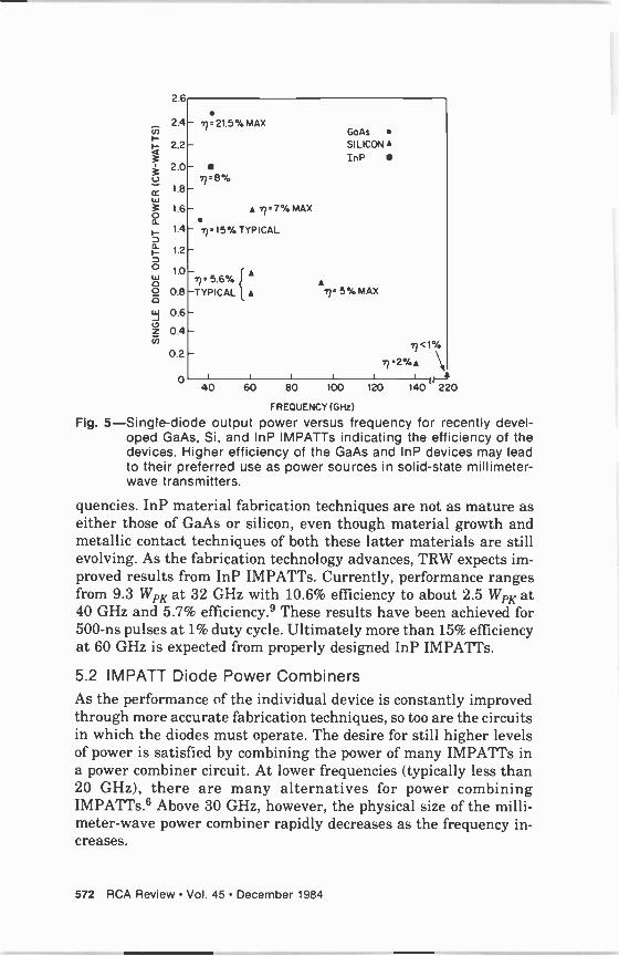
Fig. 5-Single-diode output power versus frequency for recently devel- oped GaAs, Si, and InP IMPATTs indicating the efficiency of the devices. Higher efficiency of the GaAs and InP devices may lead to their preferred use as power sources in solid-state millimeter - wave transmitters.
quencies. InP material fabrication techniques are not as mature as either those of GaAs or silicon, even though material growth and metallic contact techniques of both these latter materials are still evolving. As the fabrication technology advances, TRW expects im- proved results from InP IMPATTs. Currently, performance ranges from 9.3 WPK at 32 GHz with 10.6% efficiency to about 2.5 WPK at 40 GHz and 5.7% efficiency.9 These results have been achieved for 500-ns pulses at 1% duty cycle. Ultimately more than 15% efficiency at 60 GHz is expected from properly designed InP IMPATTs.
5.2 IMPATT Diode Power Combiners As the performance of the individual device is constantly improved through more accurate fabrication techniques, so too are the circuits in which the diodes must operate. The desire for still higher levels of power is satisfied by combining the power of many IMPATTs in a power combiner circuit. At lower frequencies (typically less than 20 GHz), there are many alternatives for power combining IMPATTs.6 Above 30 GHz, however, the physical size of the milli- meter -wave power combiner rapidly decreases as the frequency in- creases.
572 RCA Review Vol. 45 December 1984
MILLIMETER -WAVE SYSTEMS
13
12
11
10
9
8
7
6
5
4
3
2
0 10 20 30 40 50 60 70 80
FREQUENCY (GHz)
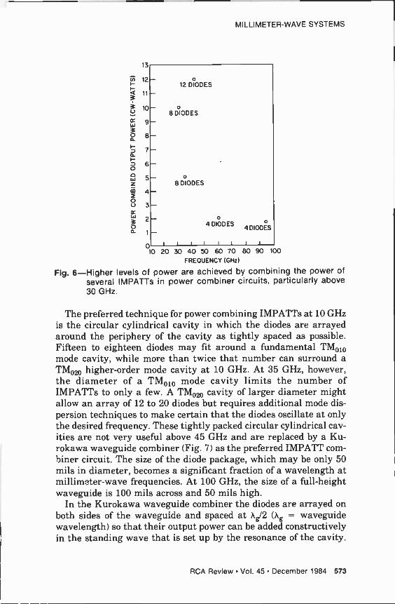
Fig. 6-Higher levels of power are achieved by combining the power of several IMPATTs in power combiner circuits, particularly above 30 GHz.
12 DIODES
0
8 DIODES
0 8 DIODES
o 4 DIODES
4DIODES
i I
90 100
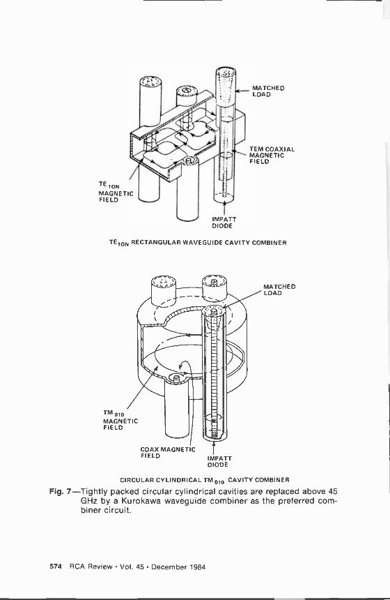
The preferred technique for power combining IMPATTs at 10 GHz is the circular cylindrical cavity in which the diodes are arrayed around the periphery of the cavity as tightly spaced as possible. Fifteen to eighteen diodes may fit around a fundamental TMo10 mode cavity, while more than twice that number can surround a TM020 higher -order mode cavity at 10 GHz. At 35 GHz, however, the diameter of a TMoto mode cavity limits the number of IMPATTs to only a few. A TM020 cavity of larger diameter might allow an array of 12 to 20 diodes but requires additional mode dis- persion techniques to make certain that the diodes oscillate at only the desired frequency. These tightly packed circular cylindrical cav- ities are not very useful above 45 GHz and are replaced by a Ku- rokawa waveguide combiner (Fig. 7) as the preferred IMPATT com- biner circuit. The size of the diode package, which may be only 50 mils in diameter, becomes a significant fraction of a wavelength at millimeter -wave frequencies. At 100 GHz, the size of a full -height waveguide is 100 mils across and 50 mils high.
In the Kurokawa waveguide combiner the diodes are arrayed on both sides of the waveguide and spaced at XgJ2 (Xg = waveguide wavelength) so that their output power can be added constructively in the standing wave that is set up by the resonance of the cavity.
RCA Review Vol. 45 December 1984 573
TE ION MAGNETIC FIELD
IMPATT DIODE
MATCHED LOAD
TEM COAXIAL MAGNETIC FIELD
TE1ON RECTANGULAR WAVEGUIDE CAVITY COMBINER
TM oto MAGNETIC FIELD
COAX MAGNETIC FIELD IMPATT
DIODE
MATCHED LOAD
CIRCULAR CYLINDRICAL TM Oto CAVITY COMBINER
Fig. 7-Tightly packed circular cylindrical cavities are replaced above 45 GHz by a Kurokawa waveguide combiner as the preferred com- biner circuit.
574 RCA Review Vol. 45 December 1984
MILLIMETER -WAVE SYSTEMS
TRW has reported 11 Wew with 12 silicon IMPATTs at 41 GHz in
such a Kurokawa waveguide combiner, and at about 60 GHz a four - diode combiner provided about 2 Wc, from silicon IMPATTs (see Fig. 6). Two notable results were reported for W -band Kurokawa waveguide power combiners. Hughes achieved 63 Wpk from four two - diode waveguide combiners in a network of hybrid waveguide cou-
plers.11,12 This result was for low -duty -cycle operation (<1 percent) and pulsewidth of 50 to 100 ns. Raytheon recently reported 1.89 Wpk from a four -diode power combiner at duty cycles from five to 35%
and easily tunable from 90 to 99 GHz.13 The long pulsewidth and high -duty -cycle operation approached CW-like operation. A newly designed precision tuning element was used to facilitate the rapid tuning of the silicon IMPATTs used in the combiner. At 140 GHz,
an experimental four -diode combiner has achieved 9.2 Wpk and an experimental two -diode Hughes combiner has achieved 5.2 Wpk at low duty cycles and short pulsewidths.
As a more detailed understanding of the interaction of the IMPATT and the power combiner circuit is established, higher per- formance circuits with improved combining efficiency and broader bandwidth performance will be achieved. One of the limiting factors of IMPATT performance is the physical package in which the diode is mounted. The package acts like a resonant circuit so that the parasitic inductance of the IMPATT beam leads or bonding wires and the parasitic capacitance of the quartz or ceramic ring limit the bandwidth of the diodes' operation. Simulations of the device physics of IMPATT diodes show that it is inherently a broadband device. At 20 GHz and 40 GHz, bandwidths in excess of 20% and 10%, respectively, have been achieved in custom -designed single - diode amplifier circuits. As the desired frequency increases and the package becomes a substantial fraction of a wavelength, the detri- mental bandwidth -limiting parasítícs are a serious concern. Addi-
tional research and development of low parasitic packages will be valuable.
6. What Next for Higher Power?
As the development of better and higher performance IMPATTs progresses, an assessment of the potential capabilities is important. What material growth techniques are the most promising? What are the expected physical limitations?
Ion -beam implantation of selected dopants is a very effective way of achieving highly doped layers. The InP diodes discussed above are fabricated by ion implantation. This process, however, usually
RCA Review Vol. 45 December 1984 575
40
35
30
RAYTHEON
- VARIAN
GaAs
25
20- RAYTHEON
15-0 SILICON HP
10-
RCA°
5-
\ \
o \ BELL \ o °°HUGHES o
FOR GaAs Si o
o o
HUGHES 0 1 I l a I i° I i
10 20 40 60 100 200 400 1000 FREQUENCY (GHz)
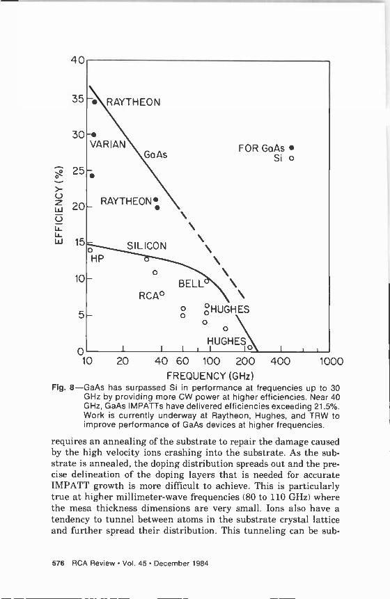
Fig. 8-GaAs has surpassed Si in performance at frequencies up to 30 GHz by providing more CW power at higher efficiencies. Near 40 GHz, GaAs IMPATTs have delivered efficiencies exceeding 21.5%. Work is currently underway at Raytheon, Hughes, and TRW to improve performance of GaAs devices at higher frequencies.
requires an annealing of the substrate to repair the damage caused by the high velocity ions crashing into the substrate. As the sub- strate is annealed, the doping distribution spreads out and the pre- cise delineation of the doping layers that is needed for accurate IMPATT growth is more difficult to achieve. This is particularly true at higher millimeter -wave frequencies (80 to 110 GHz) where the mesa thickness dimensions are very small. Ions also have a tendency to tunnel between atoms in the substrate crystal lattice and further spread their distribution. This tunneling can be sub-
576 RCA Review Vol. 45 December 1984
MILLIMETER -WAVE SYSTEMS
stantially, but not totally, eliminated by tilting the crystal so that tunneling paths in the lattice are not entered straight on by the ions.
Molecular Beam Epitaxy (MBE) is becoming an important tech- nique for the growth of IMPATT diodes with vertical dimensions having tenths of microns resolution.14 Bell Laboratories fabricated 10 GHz MBE IMPATTs in 1974.14 More recently Varian has pro- duced high power X -band IMPATTs and K -band IMPATTs designed for operation above 20 GHz by MBE.15 The unique characteristics of MBE will make it a viable technique for growing millimeter - wave GaAs IMPATTs in the 50 to 100 GHz range16 (Fig. 8). Ray- theon is currently fabricating GaAs IMPATTs above 60 GHz by MBE.
Molecular beam epitaxy is an ultrahigh vacuum technique for the evaporation of constituent elements of semiconductor compounds. Thin films with controlled dimensions and characteristics are de- posited on substrates. GaAs and related III -V compounds are com- monly grown in MBE systems.
When GaAs is evaporated, the Ga and As dissociate. So it is very difficult to evaporate GaAs onto GaAs. A method of constructing a GaAs layer is therefore necessary. In MBE, the Ga and As (as well as other elements used to dope the desired film) are thermally evap- orated from individual crucibles or cells. These separate cells create molecular beams that impinge on the substrate surface at controlled flux densities based on the evaporation rate due to the temperature of each cell. The recombination of the constituent elements results in a stoichiometric compound, and a layer of desired doping density is achieved. High purity layers can be grown as monolayers (one atom thick). MBE growth allows the abrupt transition of doping levels to be achieved. For millimeter -wave IMPATTs, especially where a Read spike or modified Read structure is desired, the abrupt transition between doping levels would allow very accurate dimen- sioning of the avalanche and drift zones. The proper phasing of secondary avalanched holes (DSA-holes) in DSA-mode operation de- pends on such accurate dimensions. The surface quality of MBE films may be superior to that of LPE (liquid -phase epitaxy) or VPE (vapor -phase epitaxy).
Currently a key question that must be answered is whether or not MBE can provide a sufficient quantity of IMPATTs in produc- tion. An alternative system of fabrication with higher throughput may be metallo-organic chemical vapor -phase deposition (MOCVD) where the growth process is more like regular chemical vapor -phase growth techniques.
RCA Review Vol. 45 December 1984 577
It may be possible to grow heterojunctions or superlattice struc- tures that can tailor the propagation velocity of holes and electrons for still higher performance GaAs IMPATTs up to and beyond 100 GHz. Techniques for growing InP IMPATTs by MBE or MOCVD would provide a very favorable alternative to the less accurate ion - implantation methods.
If accurately doped submicron layers are achieved by MBE for 100 GHz GaAs IMPATTs and the physics of the DSA mode are applied, the predicted performance for such IMPATTs is more than 1 W of CW power at 17 to 20% efficiency. Such a diode would elim- inate the need to power combine many diodes of lesser power. High - power modulators used on diodes of considerably lower efficiency (-5% at 94 GHz) would no longer be needed. Additional radar or seeker range could be achieved by power combining this more pow- erful IMPATT.
The advent and evolution of the IMPATT diode as a millimeter - wave power source has made the possibility of small, lightweight, all weather, reliable, and effective millimeter -wave systems a reality.
References:
1 J. B. Schultz, "International Competition Heats Up for Millimeter Wave Muni- tions," Defense Electronics, June 1984, pp. 100-110. 2 J. B. Schultz, "MILSTAR Progresses Despite High Cost and Technological Risks," Defense Electronics, June 1984, pp. 92-98. 3 P. Bhartia and I. J. Bahl, Millimeter Wave Engineering and Applications, 1st. ed., John Wiley and Sons, Inc., NY (1984). 4 J. G. Wiltse, "Millimeter Wave Technology and Applications," Microwave J., 22, No. 8, p. 39, Aug. 1979. 5 1984 Hughes Aircraft Millimeter -Wave Products Catalog, Introduction, pp. 2-3. 6 G. R. Thoren, "IMPATTs Combine to Power Systems," MSN, 10, p. 110, Oct. 1980. 7 G. R. Thoren, G. C. Dalman, and C. A. Le, "Delayed Secondary Avalanche Effects
in Millimeter -Wave GaAs IMPATT Diodes," IEEE Elec. Device Lett., EDL-2, p. 10, Jan. 1981. 8 G. R. Thoren, Trans. Advances in Ant. and Microwave Symp., Phila., PA, May 1981. 9 F. B. Fank, et al., 8th Biennial Cornell Conf., pp. 385-394 (1981). 10 J. J. Berenz and P. A. Blakey, 8th Biennial Cornell Conf., pp. 395-404 (1981). 11 H. C. Yen and K. Chang, MMT-S Symp. Digest, pp. 341-346 (1981). t2 H. C. Yen and K. Chang, "A 63-W W -Band Injection -Locked Pulsed Solid -State Transmitter," IEEE MTT-S Trans., MTT-29, p. 1292, Dec. 1981. 13 G. R. Thoren and M. J. Virostko, MMT-S Symp. Digest (1982). 14 K. Chang et al., MMT-S Symp. Digest (1981). 15 A. Y. Cho et al., "GaAs IMPATT Diodes Prepared by Molecular Beam Epitaxy," Appl. Phy. Lett., 25, p. 224, Aug. 1974. 16 T. L. Hierl and C. M. Collins, 7th Biennial Cornell Conf., pp. 369-378 (1979). 17 A. Y. Cho, MBE Workshop, Cornell University (1980).
578 RCA Review Vol. 45 December 1984
Millimeter -Wave Monolithic Passive Circuit Components
S. C. Binari, R. E. Neidert, G. Kelner, and J. B. Boos Naval Research Laboratory, Washington, DC 20375-5000
Abstract-Several mm -wave passive circuit elements have been designed, fabricated, and tested. The circuit elements were designed in
a microstrip format and cover the 75- to 150-GHz frequency range. They consist of a terminated 50-1Z transmission line, a
Wilkinson splitter, a Lange coupler, and a sum/difference net- work. The test results on these components demonstrate the feasibility of microstrip circuitry in this region of the mm -wave spectrum.
Introduction
In recent years, there has been considerable interest in the devel- opment of millimeter -wave monolithic circuits for potential appli- cation in areas such as radar, communication, and wideband elec- tronic warfare. Several mm -wave monolithic circuits have been demonstrated.1,2 This paper reports on the design, fabrication, and test results of passive microstrip components designed to cover the frequency range of 75 to 150 GHz. These components have been implemented with InP to exploit the potential of InP mm -wave ac- tive devices,3 but the technology is readily transferable to gallium arsenide or silicon.
Circuit Design
The components include a 50-12 terminated transmission line, a Wilkinson splitter, a Lange coupler, and a sum/difference network. A summary of the circuit design is given here; the details are pro- vided elsewhere.4 The substrate thickness was chosen to be 50 p.m
to obtain quasi-TEM operation through 420 GHz and to achieve low -
RCA Review Vol. 45 December 1984 579
impedance transmission -line segments. This value of substrate thickness is also the optimum for maximizing the unloaded Q of half -wavelength 50-e resonators in the vicinity of 100 GHz.5 The dielectric constant used in the designs was 12.55. This value of dielectric constant was determined from low- and high -frequency measurements.4.6 The low -frequency measurements were performed on a metallized rectangular slab of InP. The dielectric constant was determined by measuring the resonate frequencies of the slab from 4 to 18 GHz.6 This value was confirmed at W -band by modeling the transmission characteristics of linear and ring resonators fabricated on InP.4
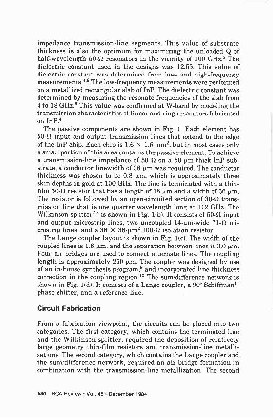
The passive components are shown in Fig. 1. Each element has 50-9 input and output transmission lines that extend to the edge of the InP chip. Each chip is 1.6 x 1.6 mm2, but in most cases only a small portion of this area contains the passive element. To achieve a transmission -line impedance of 50 it on a 50 -p.m -thick InP sub- strate, a conductor linewidth of 36 µm was required. The conductor thickness was chosen to be 0.8 p.m, which is approximately three skin depths in gold at 100 GHz. The line is terminated with a thin- film 50-11 resistor that has a length of 18 p.m and a width of 36 p.m. The resistor is followed by an open -circuited section of 30-12 trans- mission line that is one quarter wavelength long at 112 GHz. The Wilkinson splitter"s is shown in Fig. 1(b). It consists of 50-12 input and output microstrip lines, two uncoupled 14 -p.m -wide 71-52 mi- crostrip lines, and a 36 x 36-µm2 100-Il isolation resistor.
The Lange coupler layout is shown in Fig. 1(c). The width of the coupled lines is 1.6 p.m, and the separation between lines is 3.0 µm. Four air bridges are used to connect alternate lines. The coupling length is approximately 250 p.m. The coupler was designed by use of an in-house synthesis program,9 and incorporated line -thickness correction in the coupling region.10 The sum/difference network is shown in Fig. 1(d). It consists of a Lange coupler, a 90° Schiffmanl l phase shifter, and a reference line.
Circuit Fabrication
From a fabrication viewpoint, the circuits can be placed into two categories. The first category, which contains the terminated line and the Wilkinson splitter, required the deposition of relatively large geometry thin-film resistors and transmission -line metalli- zations. The second category, which contains the Lange coupler and the sum/difference network, required an air -bridge formation in combination with the transmission -line metallization. The second
580 RCA Review Vol. 45 December 1984
MILLIMETER -WAVE COMPONENTS
504 RESISTOR
H.--.4 50Nm
500 TERMINATED TRANSMISSION LINE
A/4
Z0-304
la)
LANGE COUPLER
(C)
1004 RESISTOR
I-4 50Nm
WILKINSON SPLITTER
(b)
SCHIFFMAN PHASE SHIFTER
I. --..I 100ym
4 1
REFERENCE LINE
LANGE COUPLER
2 3
SUM/DIFFERENCE HYBRID
Id)
Fig. 1-75- to 150-GHz passive circuit components.
category required much smaller line widths and is considerably more process intensive than the first category.
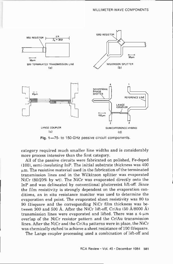
All of the passive circuits were fabricated on polished, Fe -doped (100), semi -insulating InP. The initial substrate thickness was 400 p.m. The resistive material used in the fabrication of the terminated transmission lines and in the Wilkinson splitter was evaporated NiCr (80/20% by wt). The NiCr was evaporated directly onto the InP and was delineated by conventional photoresist lift-off. Since the film resistivity is strongly dependent on the evaporation con- ditions, an in situ resistance monitor was used to determine the evaporation end point. The evaporated sheet resistivity was 80 to 90 9/square and the corresponding NiCr film thickness was be- tween 300 and 500 A. After the NiCr lift-off, Cr/Au (50 A/8000 A) transmission lines were evaporated and lifted. There was a 4 -p.m overlap of the NiCr resistor pattern and the Cr/Au transmission lines. After the NiCr and the Cr/Au patterns were in place, the NiCr was chemically etched to achieve a sheet resistance of 10012/square.
The Lange coupler processing used a combination of lift-off and
RCA Review Vol. 45 December 1984 581
nn PHOTORESIST
5000 A SILICON NITRIDE
InP
PHOTORESIST n Í NITRIDE
InP
Cr/Au
150 A 18000 \
NITRIDE
InP
PLATED Au
PHOTORESIST
200A Au NITRIDE
InP
PLATED Au
EVAPORATED Cr/Au
InP
Fig. 2-Lange coupler air -bridge fabrication sequence.
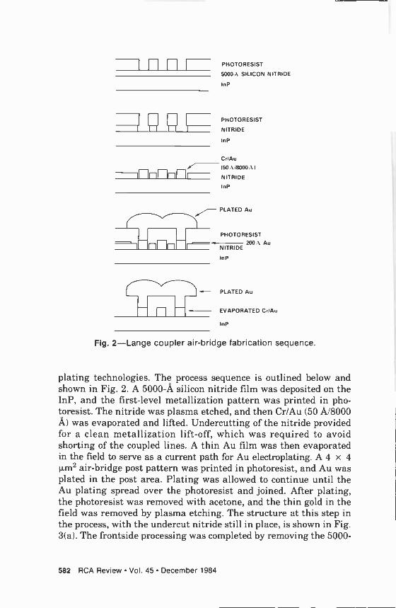
plating technologies. The process sequence is outlined below and shown in Fig. 2. A 5000-A silicon nitride film was deposited on the InP, and the first -level metallization pattern was printed in pho- toresist. The nitride was plasma etched, and then Cr/Au (50 A/8000 A) was evaporated and lifted. Undercutting of the nitride provided for a clean metallization lift-off, which was required to avoid shorting of the coupled lines. A thin Au film was then evaporated in the field to serve as a current path for Au electroplating. A 4 x 4 1.1.m2 air -bridge post pattern was printed in photoresist, and Au was plated in the post area. Plating was allowed to continue until the Au plating spread over the photoresist and joined. After plating, the photoresist was removed with acetone, and the thin gold in the field was removed by plasma etching. The structure at this step in the process, with the undercut nitride still in place, is shown in Fig. 3(a). The frontside processing was completed by removing the 5000-
i
582 RCA Review Vol. 45 December 1984
MILLIMETER -WAVE COMPONENTS
.- " " ,. .. 1 :y ,
i. . . .. ,v ,- » c+
iogrn 1m
(a) (b)
Fig. 3-Scanning electron micrographs of Lange coupler (a) with un-
dercut nitride used for lift-off still in place and (b) with completed air bridge and nitride removed.
A -thick nitride layer in buffered HF. The finished Lange coupler is
shown in Fig. 3(b). The final steps for both types of circuits are outlined below. After
the completion of the fi-ontside processing, the wafers were scribed
and mounted on a sapphire disk by means of a low -temperature wax. The wafers were lapped to a thickness of 50 µm to establish the proper transmission -line impedances. After lapping, 1.5 µm of
Al was evaporated on the backside of the wafers to serve as the microstrip ground plane. After the wafers were removed from the sapphire disk, the 1.6 x 1.6 mm2 circuits were separated and mounted on brass blocks for millimeter -wave evaluation.
Test Results
The components were tested from 75 to 110 GHz. The circuits were
interfaced to laboratory waveguide-measurement equipment through a microstrip-to-coaxial-to-waveguide transition.12 The re-
sults presented here were de -embedded to remove the characteris- tics of the transitions and the microstrip losses.
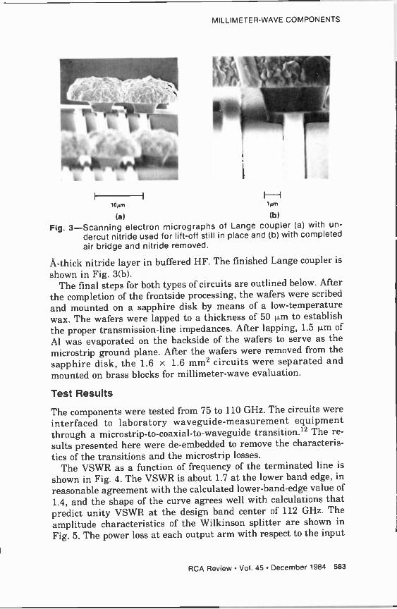
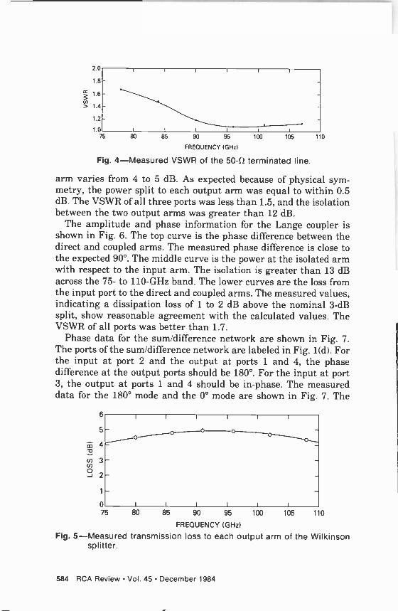
The VSWR as a function of frequency of the terminated line is
shown in Fig. 4. The VSWR ís about 1.7 at the lower band edge, in
reasonable agreement with the calculated lower -band -edge value of
1.4, and the shape of the curve agrees well with calculations that predict unity VSWR at the design band center of 112 GHz. The
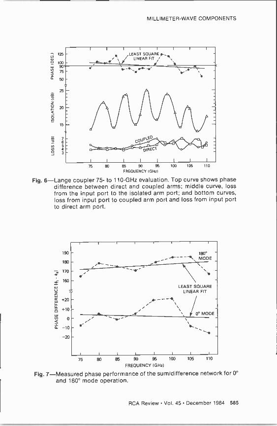
amplitude characteristics of the Wilkinson splitter ai-e shown in
Fig. 5. The power loss at each output arm with respect to the input
RCA Review Vol. 45 December 1984 583
2.0
1.8
1.6 -
1.4
1.2 - 10 l l l t l
75 80 85 90 95 100 105
FREOUENCY 1GHz)
Fig. 4-Measured VSWR of the 50-9 terminated line.
110
arm varies from 4 to 5 dB. As expected because of physical sym- metry, the power split to each output arm was equal to within 0.5 dB. The VSWR of all three ports was less than 1.5, and the isolation between the two output arms was greater than 12 dB.
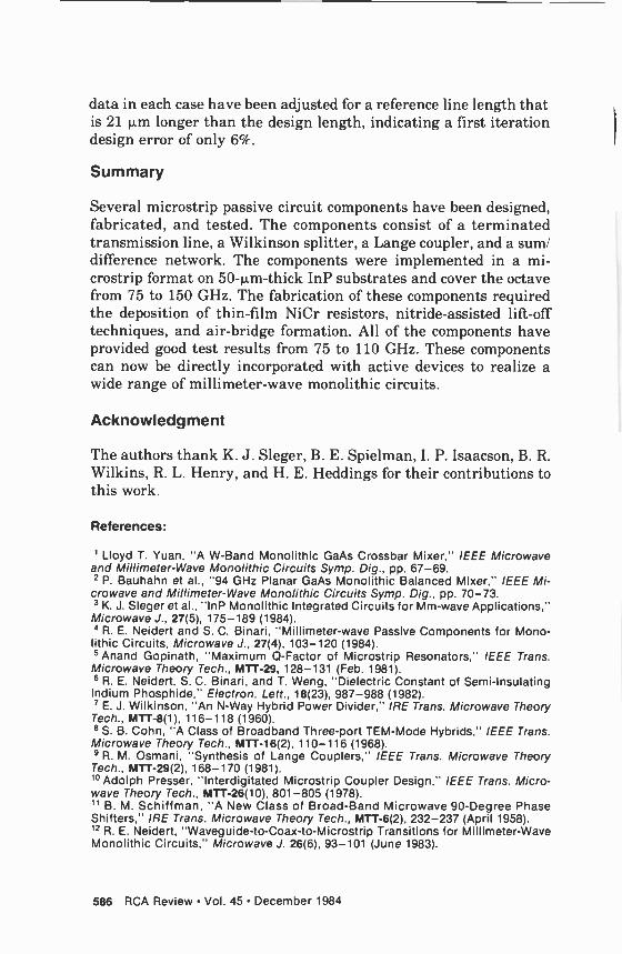
The amplitude and phase information for the Lange coupler is shown in Fig. 6. The top curve is the phase difference between the direct and coupled arms. The measured phase difference is close to the expected 90°. The middle curve is the power at the isolated arm with respect to the input arm. The isolation is greater than 13 dB across the 75- to 110-GHz band. The lower curves are the loss from the input port to the direct and coupled arms. The measured values, indicating a dissipation loss of 1 to 2 dB above the nominal 3 -dB split, show reasonable agreement with the calculated values. The VSWR of all ports was better than 1.7.
Phase data for the sum/difference network are shown in Fig. 7. The ports of the sum/difference network are labeled in Fig. 1(d). For the input at port 2 and the output at ports 1 and 4, the phase difference at the output ports should be 180°. For the input at port 3, the output at ports 1 and 4 should be in -phase. The measured data for the 180° mode and the 0° mode are shown in Fig. 7. The
6
5
o
1
_ 0--------0 c--- c c,
75 80 85 90 95 100
FREQUENCY (GHz)
Fig. 5-Measured transmission loss to each output arm of the Wilkinson splitter.
105 110
584 RCA Review Vol. 45 December 1984
MILLIMETER -WAVE COMPONENTS
v y ó
125
100 - 907 75 -
50
25
20
15
7 6 5 4 3
1 I 1
LEAST SQUARE,.. / LINEAR FIT r i d `-..rr--
cpUPtEO
1RECT
\ _
I t 1 I I I I I
75 80 85 90 95 100 105 110
FREQUENCY (GHz1
Fig. 6-Lange coupler 75- to 110-GHz evaluation. Top curve shows phase difference between direct and coupled arms; middle curve, loss from the input port to the isolated arm port; and bottom curves, loss from input port to coupled arm port and loss from input port to direct arm port.
190 - 180 - 170 - 160 -
+20 -
+10 -
0
-10 - - 20 -
1
75
-- 180° --- MODE
ti
LEAST SQUARE LINEAR FIT
0° MODE
80 85 90 95 100
FREQUENCY (GHZ)
105
I
110
Fig. 7-Measured phase performance of the sum/difference network for 0°
and 180° mode operation.
RCA Review Vol. 45 December 1984 585
data in each case have been adjusted for a reference line length that is 21 p.m longer than the design length, indicating a first iteration design error of only 6%.
Summary
Several microstrip passive circuit components have been designed, fabricated, and tested. The components consist of a terminated transmission line, a Wilkinson splitter, a Lange coupler, and a sum/ difference network. The components were implemented in a mi- crostrip format on 50 -p.m -thick InP substrates and cover the octave from 75 to 150 GHz. The fabrication of these components required the deposition of thin-film NiCr resistors, nitride -assisted lift-off techniques, and air -bridge formation. All of the components have provided good test results from 75 to 110 GHz. These components can now be directly incorporated with active devices to realize a wide range of millimeter -wave monolithic circuits.
Acknowledgment
The authors thank K. J. Sleger, B. E. Spielman, I. P. Isaacson, B. R. Wilkins, R. L. Henry, and H. E. Heddings for their contributions to this work.
References:
1 Lloyd T. Yuan, "A W -Band Monolithic GaAs Crossbar Mixer," IEEE Microwave and Millimeter -Wave Monolithic Circuits Symp. Dig., pp. 67-69. 2 P. Bauhahn et al., "94 GHz Planar GaAs Monolithic Balanced Mixer," IEEE Mi- crowave and Millimeter -Wave Monolithic Circuits Symp. Dig., pp. 70-73. 3 K. J. Steger et al., "InP Monolithic Integrated Circuits for Mm -wave Applications," Microwave J., 27(5), 175-189 (1984). 4 R. E. Neidert and S. C. Binari, "Millimeter -wave Passive Components for Mono- lithic Circuits, Microwave J., 27(4), 103-120 (1984).
Anand Gopinath, "Maximum 0 -Factor of Microstrip Resonators," IEEE Trans. Microwave Theory Tech., MTT-29, 128-131 (Feb. 1981). 6 R. E. Neidert, S. C. Binari, and T. Weng, "Dielectric Constant of Semi -Insulating Indium Phosphide," Electron. Lett., 18(23), 987-988 (1982). 7 E. J. Wilkinson, "An N -Way Hybrid Power Divider," IRE Trans. Microwave Theory Tech., MTT-8(1), 116-118 (1960). 8 S. B. Cohn, "A Class of Broadband Three -port TEM-Mode Hybrids," IEEE Trans. Microwave Theory Tech., MTT-16(2), 110-116 (1968). 9 R. M. Osmani, "Synthesis of Lange Couplers," IEEE Trans. Microwave Theory Tech., MTT-29(2), 168-170 (1981). 10 Adolph Presser, "Interdigitated Microstrip Coupler Design," IEEE Trans. Micro- wave Theory Tech., MTT-26(10), 801-805 (1978). 11 B. M. Schiffman, "A New Class of Broad -Band Microwave 90 -Degree Phase Shifters," IRE Trans. Microwave Theory Tech., MTT-6(2), 232-237 (April 1958). 12 R. E. Neidert, "Waveguide-to-Coax-to-Microstrip Transitions for Millimeter -Wave Monolithic Circuits," Microwave J. 26(6), 93-101 (June 1983).
586 RCA Review Vol. 45 December 1984
A Silicon Technology for Millimeter -Wave Monolithic Circuits*
Paul J. Stabile and Arye Rosen RCA Laboratories, Princeton, NJ 08540
Abstract-A silicon millimeter -wave integrated -circuit (SIMMWIC) tech- nology that includes high-energy ion implantation and pulsed - laser annealing, secondary ion mass spectrometry (SIMS) pro- file diagnostics, and novel wafer thinning has been developed. This technology has been applied to a SIMMWIC single -pole single -throw (SPST) switch and to IMPATT and p -i -n diode fab- rication schemes. Thus, the SIM MWIC technology is a proven base for monolithic millimeter -wave sources and control circuit applications.
1. Introduction
The success of future millimeter -wave systems depends on the avail- ability of reproducible, low-cost circuits. To date, millimeter -wave circuits have been commercially available as discrete components mounted in a waveguíde, an inherently expensive transmission line medium. The silicon millimeter -wave integrated -circuit (SIMMWIC) technology offers a low-cost high -yield approach.' -3
Ingredients of the SIMMWIC technology are selective ion im- plantation, pulsed -laser annealing, secondary ion mass spectrom- etry (SIMS) profile diagnostics, and novel wafer thinning. The use of selective ion implantation and laser annealing over a part of the wafer assures that the high resistivity of the other parts is retained. This is essential for integrating millimeter -wave devices with low -
loss microstrip circuits on silicon. Secondary ion mass spectrometry (SIMS) profile diagnostics provide the necessary feedback to coor-
This paper is based in part on papers published in the 13th European Microwave Conference Proceedings, 1983; IEEE MTT-S Digest, 1984; and Electronics Letters, 1984. See Refs. 1-3.
RCA Review Vol. 45 December 1984 587
dinate the many ion implantations that make up the active device structures. Thinning a portion of the wafer to 2 or 3 p.m is necessary to fabricate the all -ion -implanted IMPATT diode, as well as to min- imize the thermal resistance.
In this paper, we demonstrate the first SIMMWICs. These mono- lithic circuits are single -pole single -throw (SPST) switches that op- erate in Q band (33-50 GHz). Performance includes 20% instan- taneous 3 -dB bandwidth, with a minimum isolation of 21.6 dB.
In addition, we describe a 60-GHz oscillator circuit utilizing 2000 12 cm silicon wafers as substrates. This microstrip circuit, in con- junction with a discrete silicon IMPATT device, validates our mono- lithic in -silicon concept.
We also characterize, using cross-sectional transmission electron microscopy (TEM), the defects found in the regions of the silicon that were implanted with phosphorus at high energy and high dose. These implanted structures (implant energy of 1.5 MeV, fluence of 3 x 10¹⁵ atoms cm -3) are necessary for the creation of deep contact layers in the all -implanted IMPATT diodes.
In addition, we also demonstrate the fabrication of several types of p -i -n and IMPATT diodes by means of SIMMWIC technology. These include both vertical and horizontal (lateral) p -i -n diodes, as well as all -ion -implanted and laser -annealed IMPATT diodes.
2. High -Resistivity Silicon for Monolithic Sources
The use of high -resistivity silicon for monolithic circuits was first seriously investigated in 1965.4 This approach was abandoned when it was found that the processing steps of epitaxial growth signifi- cantly lowered the resistivity of the silicon. To preserve the required high resistivity of the bulk silicon material, the processing temper- ature must not exceed 800°C. The techniques we are describing for processing and analyzing silicon wafers include ion implantation, laser annealing, SIMS, and TEM." They permit fabricating the ac- tive devices without degrading the high -resistivity substrate. The high -resistivity silicon is then used as a substrate on which passive microstríp circuits are printed to complete the monolithic compo- nent for EHF.
3. SIMMWIC SPST Switch
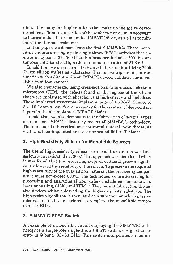
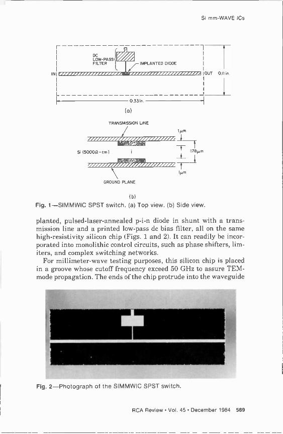
An example of a monolithic circuit employing the SIMMWIC tech- nology is a single -pole single -throw (SPST) switch, designed to op- erate in Q band (33-50 GHz). This switch incorporates an ion-im-
588 RCA Review Vol. 45 December 1984
Si mm -WAVE ICs
r DC LOW-PASS FILTER
A
/lam IMPLANTED DIODE
1
INIV/////////////////// //////////////////////i1 OUT 0.11 in.
I L J 0.33 in.
(0)
TRANSMISSION LINE
i/i//iiii/ ll¡i/il/iiiiiir. Si (5000R -cm) 178µm
n,, _. l /////////>//?/7///z/z////
lµm
GROUND PLANE
(b)
Fig. 1-SIMMWIC SPST switch. (a) Top view. (b) Side view.
planted, pulsed -laser -annealed p -i -n diode in shunt with a trans- mission line and a printed low-pass de bias filter, all on the same high -resistivity silicon chip (Figs. 1 and 2). It can readily be incor- porated into monolithic control circuits, such as phase shifters, lim- iters, and complex switching networks.
For millimeter -wave testing purposes, this silicon chip is placed in a groove whose cutoff frequency exceed 50 GHz to assure TEM- mode propagation. The ends of the chip protrude into the waveguide
0
Fig. 2-Photograph of the SIMMWIC SPST switch.
RCA Review Vol. 45 December 1984 589
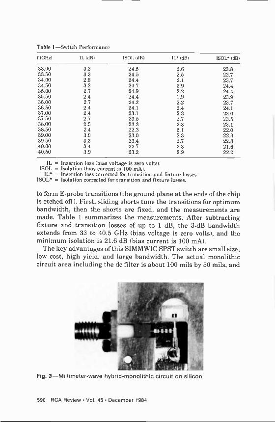
Table 1 -Switch Performance
f (GHz) IL (dB) ISOL (dB) IL* (dB) ISOL* (dB)
33.00 3.3 24.5 2.6 23.8 33.50 3.3 24.5 2.5 23.7 34.00 2.8 24.4 2.1 23.7 34.50 3.2 24.7 2.9 24.4 35.00 2.7 24.9 2.2 24.4 35.50 2.4 24.4 1.9 23.9 36.00 2.7 24.2 2.2 23.7 36.50 2.4 24.1 2.4 24.1 37.00 2.4 23.1 2.3 23.0 37.50 2.7 23.5 2.7 23.5 38.00 2.5 23.3 2.3 23.1 38.50 2.4 22.3 2.1 22.0 39.00 3.0 23.0 2.3 22.3 39.50 3.3 23.4 2.7 22.8 40.00 3.4 22.7 2.3 21.6 40.50 3.9 23.2 2.9 22.2
IL = Insertion loss (bias voltage is zero volts). ISOL = Isolation (bias current is 100 mA).
IL' = Insertion loss corrected for transition and fixture losses. ISOL* = Isolation corrected for transition and fixture losses.
to form E -probe transitions (the ground plane at the ends of the chip is etched off). First, sliding shorts tune the transitions for optimum bandwidth, then the shorts are fixed, and the measurements are made. Table 1 summarizes the measurements. After subtracting fixture and transition losses of up to 1 dB, the 3 -dB bandwidth extends from 33 to 40.5 GHz (bias voltage is zero volts), and the minimum isolation is 21.6 dB (bias current is 100 mA).
The key advantages of this SIMMWIC SPST switch are small size, low cost, high yield, and large bandwidth. The actual monolithic circuit area including the dc filter is about 100 mils by 50 mils, and
140
1'
Fig. 3 -Millimeter -wave hybrid -monolithic circuit on silicon.
590 RCA Review Vol. 45 December 1984
Si mm -WAVE ICs
HIGH-ENERGY ION IMPLANTATION
111
METALLIZATION
1 1 1 n
LASER ANNEALING
WAFER THINNING
UEZZJ.
1 I
,
1 1 o t 1 1
HIGH-ENERGY ION IMPLANTATION
BACK METALLIZATION
111 MASK
LASER ANNEALING
PATTERN CIRCUIT FABRICATE AIRBRIDGES
1
DIODES
CIRCUITS
Fig. 4-Fabrication steps for silicon monolithic integrated circuits.
the substrate material is readily available silicon. The processing steps are reliable high -yield techniques, and the yield (based on
static parameters) for the first run was about 90%. The shunt - mounted p -i -n diode switch realized in this manner is capable of operating over the waveguide band without any performance deg- radation.
4. Hybrid Monolithic Circuit Chip
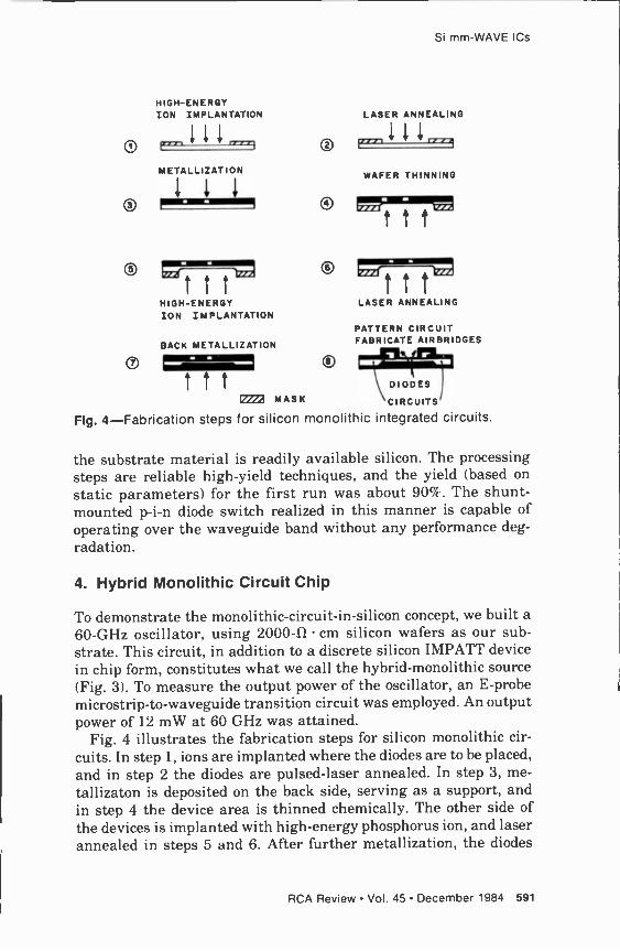
To demonstrate the monolithic -circuit -in -silicon concept, we built a 60-GHz oscillator, using 2000-9 cm silicon wafers as our sub- strate. This circuit, in addition to a discrete silicon IMPATT device in chip form, constitutes what we call the hybrid -monolithic source (Fig. 3). To measure the output power of the oscillator, an E -probe microstrip-to-waveguide transition circuit was employed. An output power of 12 mW at 60 GHz was attained.
Fig. 4 illustrates the fabrication steps for silicon monolithic cir- cuits. In step 1, ions are implanted where the diodes are to be placed, and in step 2 the diodes are pulsed -laser annealed. In step 3, me-
tallizaton is deposited on the back side, serving as a support, and in step 4 the device area is thinned chemically. The other side of the devices is implanted with high-energy phosphorus ion, and laser annealed in steps 5 and 6. After further metallization, the diodes
RCA Review Vol. 45 December 1984 591
are completed, along with circuits at the edge of the wafer. Note that the substrate allocated for processing the circuits has been unharmed (since it never experienced high temperature); thus the devices can be made integral parts of the circuits.
5. TEM Annealing Study of Silicon Implanted with Phosphorus at High Energies
We have studied the worst possible conditions that can affect device properties, namely high-energy and high -dose ion implantation. It is important to note that the combination of high -dose and high- energy ion implantation is used only to create the contact layers of the IMPATT devices, the feasibility of which has been demon- strated. The drift region of the IMPATT diode may require high- energy implantation, but at a dose well below 1013 cm -2 (see Table 2 in Section 6.2). Therefore, no serious crystal damage is expected, and device properties will not be affected.
The damage found in the regions of the silicon implanted with high-energy phosphorus ions at a high dose before and after laser annealing have been characterized by transmission electron mi- croscopy (TEM).
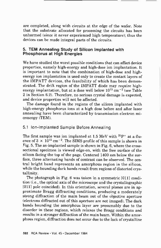
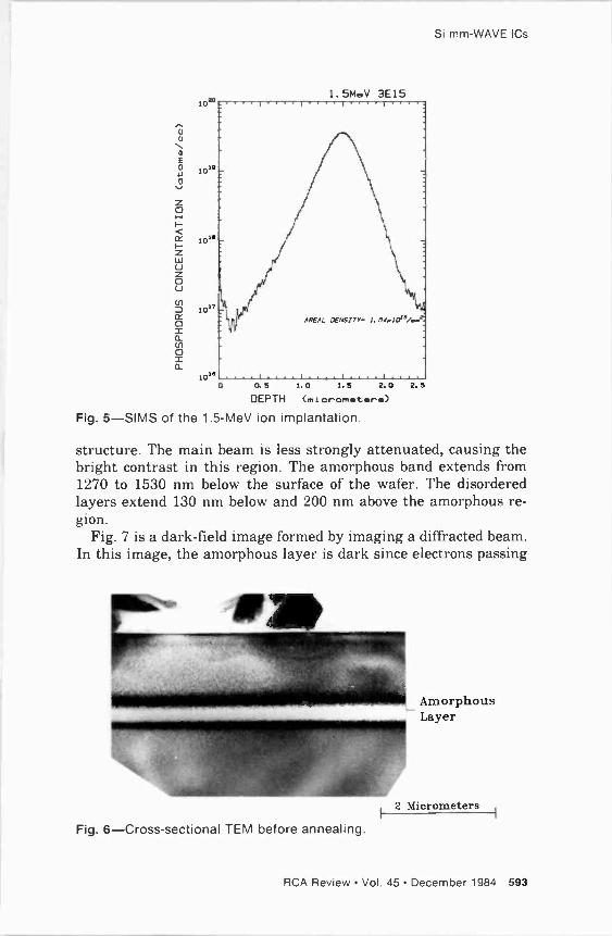
5.1 Ion -Implanted Sample Before Annealing
The first sample was ion implanted at 1.5 MeV with 31P+ at a flu- ence of 3 x 1015 cm -2. The SIMS profile of this sample is shown in Fig. 5. The as -implanted sample is shown in Fig. 6, where the cross- sectional specimen is viewed edge -on, with the free surface of the silicon facing the top of the page. Centered 1400 nm below the sur- face, three alternating bands of contrast can be observed. The cen- tral bright band represents an amorphous region in the silicon, while the bounding dark bands result from regions of distorted crys- tallinity.
The photograph in Fig. 6 was taken in a symmetric 10111 condi- tion (i.e., the optical axis of the microscope and the crystallographic 10111 pole coincided). In this orientation, several planes are in ap- proximate Bragg diffracting conditions, producing a moderately strong diffraction of the main beam out of the objective aperture (electrons diffracted out of this aperture are not imaged). The dark bands bounding the amorphous layer are presumably due to the disorder in these regions, which relaxes the Bragg conditions and results in a stronger diffraction of the main beam. Within the amor- phous region, diffraction does not occur due to the lack of crystalline
592 RCA Review Vol. 45 December 1984
Si mm -WAVE ICs
IOmF . . . I . . .
T
1. 5MeV 3E15
AREAL DENSITY- 1. 6Ix10"/w
101e O 0.5 1.0 1.5
(micromilter) DEPTH
Fig. 5-SIMS of the 1.5-MeV ion implantation.
structure. The main beam is less strongly attenuated, causing the bright contrast in this region. The amorphous band extends from 1270 to 1530 nm below the surface of the wafer. The disordered layers extend 130 nm below and 200 nm above the amorphous re- gion.
Fig. 7 is a dark -field image formed by imaging a diffracted beam. In this image, the amorphous layer is dark since electrons passing
_
Fig. 6-Cross-sectional TEM before annealing.
Amorphous Layer
2 Micrometers
RCA Review Vol. 45 December 1984 593
- . _ 2 -ir -- Amorphous - Layer
2 Micrometers
Fig. 7-Dark-field cross-sectional TEM before annealing.
through this region are not diffracted. The crystalline regions below -and above the amorphous layer display contrasts similar to each other, indicating that they are in the same crystalline orientation.
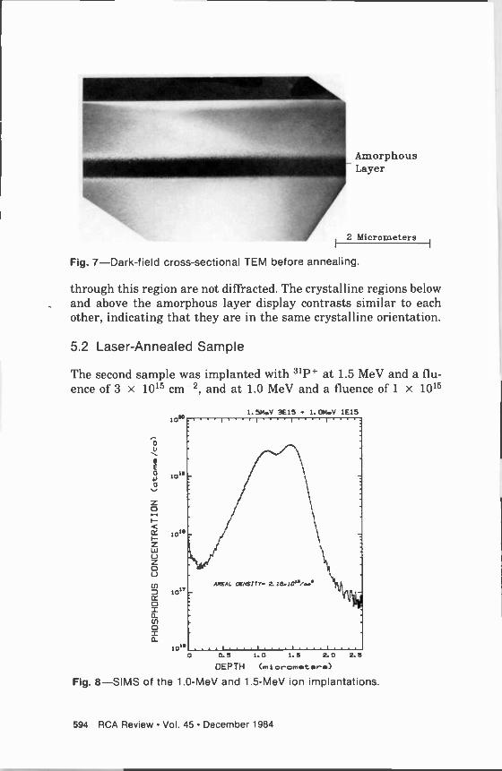
5.2 Laser -Annealed Sample
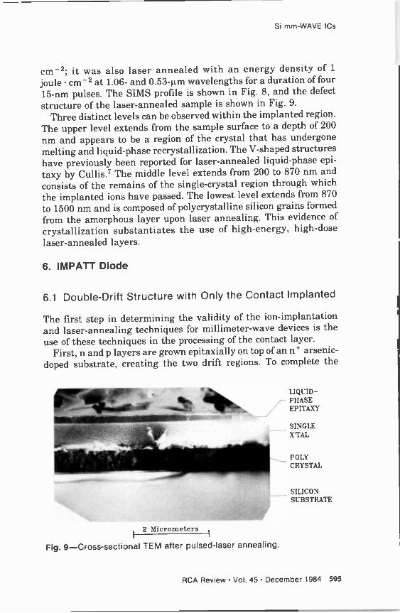
The second sample was implanted with 31P4 at 1.5 MeV and a flu- ence of 3 x 1015 cm -2, and at 1.0 MeV and a fluence of 1 x 10¹⁵
102°
101
1.5M.V 3E15 1.0M.V 1E15
1
101U
1017
101a 0.5 1.0 1.5 2.0 2.5
DEPTH (micrometers)
Fig. 8-SIMS of the 1.0-MeV and 1.5-MeV ion implantations.
594 RCA Review Vol. 45 December 1984
Si mm -WAVE ICs
cm -2; it was also laser annealed with an energy density of 1
joule cm -2 at 1.06- and 0.53 -p.m wavelengths for a duration of four
15-nm pulses. The SIMS profile is shown in Fig. 8, and the defect
structure of the laser -annealed sample is shown in Fig. 9.
Three distinct levels can be observed within the implanted region.
The upper level extends from the sample surface to a depth of 200
nm and appears to be a region of the crystal that has undergone melting and liquid -phase recrystallization. The V-shaped structures have previously been reported for laser -annealed liquid -phase epi-
taxy by Cullis.7 The middle level extends from 200 to 870 nm and
consists of the remains of the single -crystal region through which
the implanted ions have passed. The lowest level extends from 870
to 1500 nm and is composed of polycrystalline silicon grains formed
from the amorphous layer upon laser annealing. This evidence of
crystallization substantiates the use of high-energy, high -dose
laser -annealed layers.
6. IMPATT Diode
6.1 Double -Drift Structure with Only the Contact Implanted
The first step in determining the validity of the ion -implantation and laser -annealing techniques for millimeter -wave devices is the use of these techniques in the processing of the contact layer.
First, n and p layers are grown epitaxially on top of an n+ arsenic - doped substrate, creating the two drift regions. To complete the
LIQUID - PHASE EPITAXY
ti
2 Micrometers
Fig. 9-Cross-sectional TEM after pulsed -laser annealing.
SINGLE X'TAL
POLY CRYSTAL
SILICON SUBSTRATE
RCA Review Vol. 45 December 1984 595
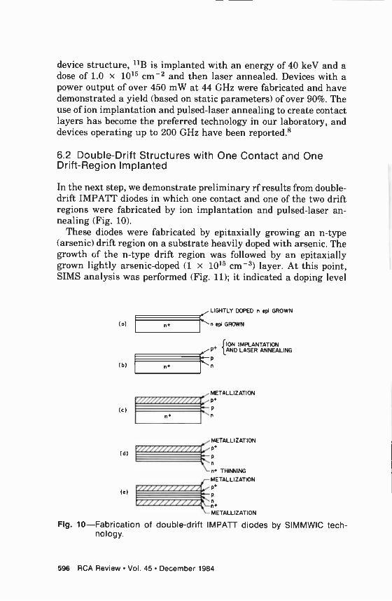
device structure, "B is implanted with an energy of 40 keV and a dose of 1.0 x 1015 cm -2 and then laser annealed. Devices with a power output of over 450 mW at 44 GHz were fabricated and have demonstrated a yield (based on static parameters) of over 90%. The use of ion implantation and pulsed -laser annealing to create contact layers has become the preferred technology in our laboratory, and devices operating up to 200 GHz have been reported.8
6.2 Double -Drift Structures with One Contact and One Drift -Region Implanted
In the next step, we demonstrate preliminary rf results from double - drift IMPATT diodes in which one contact and one of the two drift regions were fabricated by ion implantation and pulsed -laser an- nealing (Fig. 10).
These diodes were fabricated by epitaxially growing an n -type (arsenic) drift region on a substrate heavily doped with arsenic. The growth of the n -type drift region was followed by an epitaxially grown lightly arsenic -doped (1 x 1015 cm -3) layer. At this point, SIMS analysis was performed (Fig. 11); it indicated a doping level
(a)
(b)
(c)
(d)
(e)
n*
n*
LIGHTLY DOPED n epi GROWN
e:l GROWN
ION IMPLANTATION P' AND LASER ANNEALING
P
n
METALLIZATION
D
METALLIZATION
D*
n* THINNING
METALLIZATION
D*
D.
`n* METALLIZATION
Fig. 10-Fabrication of double -drift IMPATT diodes by SIMMWIC tech- nology.
596 RCA Review Vol. 45 December 1984
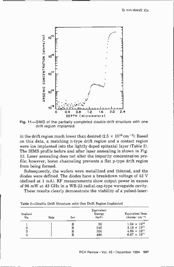
Si mm -WAVE ICs
1012
1017
101
101
f^+.. 1,.'
j,¡¿yl i]I l+. .I I I i
0 0.4 0.8 1.2 1.6 2.0 2.4 DEPTH (micrometers)
Fig. 11-SIMS of the partially completed double -drift structure with one drift region implanted.
in the drift region much lower than desired (2.5 x 1016 cm -3). Based on this data, a matching n -type drift region and a contact region were ion implanted into the lightly doped epitaxial layer (Table 2). The SIMS profile before and after laser annealing is shown in Fig. 12. Laser annealing does not alter the impurity concentration pro- file; however, boron channeling prevents a flat p -type drift region from being formed.
Subsequently, the wafers were metallized and thinned, and the diodes were defined. The diodes have a breakdown voltage of 42 V (defined at 1 mA). RF measurements show output power in excess of 96 mW at 43 GHz in a WR-22 radial -cap -type waveguide cavity.
These results clearly demonstrate the viability of a pulsed -laser -
Table 2-Double Drift Structure with One Drift Region Implanted
Equivalent Implant Energy Equivalent Dose
No. Side Ion (keV) (Atoms cm -2)
1 I B 50 1.54 x 10¹⁵ 2 I B 240 3.16 x 10¹¹
3 I B 350 4.86 x 10¹¹
4 I B 480 6.67 x 10¹¹
RCA Review Vol. 45 :')ecember 1984 597
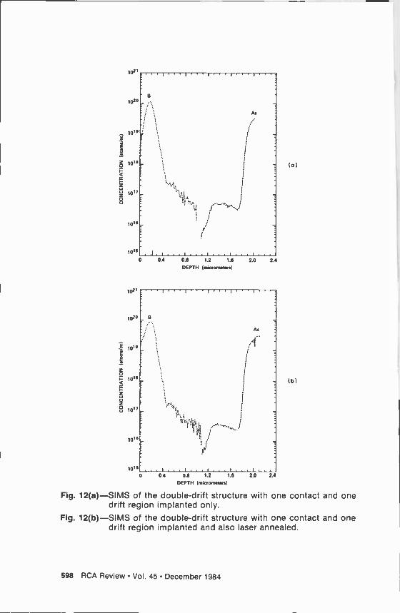
1031
1020
1019
E
ZO 1018
4 ¢ f Z
o U
lÓl7
1016
1015
1021
1020
o Q
1 0"
z U Z
1017
1016
1015
(
0.4 0.8 1.2 1.6
DEPTH (micrometers)
As
2.0 2.4
rrrrrT-rr ' ,
(0)
(b)
0.4 0.8 1.2 1.6 2.0 T.4
DEPTH (micrometers)
Fig. 12(a)-SIMS of the double -drift structure with one contact and one drift region implanted only.
Fig. 12(b)-SIMS of the double -drift structure with one contact and one drift region implanted and also laser annealed.
598 RCA Review Vol. 45 December 1984
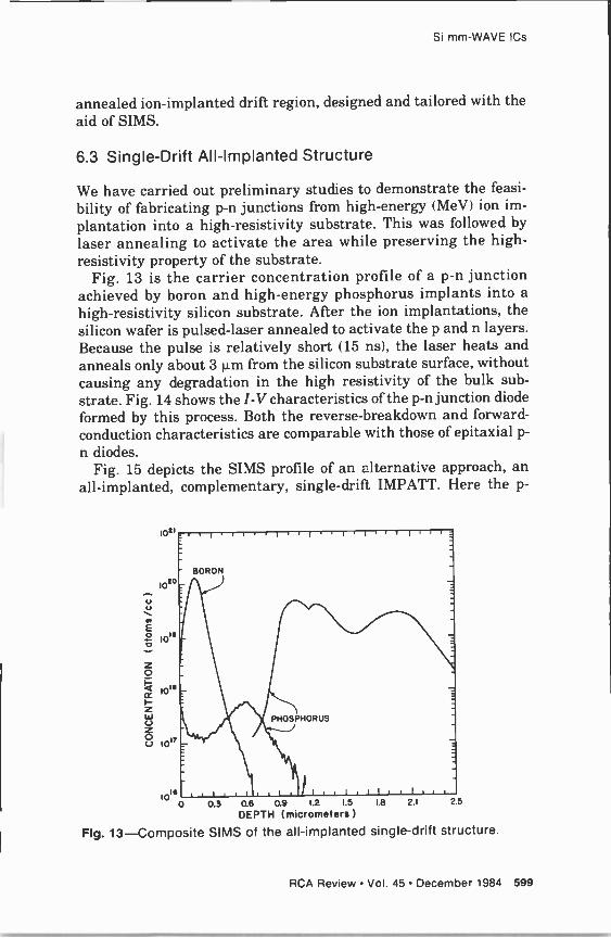
Si mm -WAVE ICs
annealed ion -implanted drift region, designed and tailored with the aid of SIMS.
6.3 Single -Drift All -Implanted Structure
We have carried out preliminary studies to demonstrate the feasi- bility of fabricating p -n junctions from high-energy (MeV) ion im-
plantation into a high -resistivity substrate. This was followed by
laser annealing to activate the area while preserving the high - resistivity property of the substrate.
Fig. 13 is the carrier concentration profile of a p -n junction achieved by boron and high-energy phosphorus implants into a
high -resistivity silicon substrate. After the ion implantations, the silicon wafer is pulsed -laser annealed to actívate the p and n layers. Because the pulse is relatively short (15 ns), the laser heats and anneals only about 3µm from the silicon substrate surface, without causing any degradation in the high resistivity of the bulk sub- strate. Fig. 14 shows the I -V characteristics of the p -n junction diode formed by this process. Both the reverse -breakdown and forward - conduction characteristics are comparable with those of epitaxial p -
n diodes. Fig. 15 depicts the SIMS profile of an alternative approach, an
all -implanted, complementary, single -drift IMPATT. Here the p-
IOY1t
BORON
0.3 0.6 0.9 1.2 1.5
DEPTH (micrometers )
1.8 2.1 2 5
Fig. 13-Composite SIMS of the all -implanted single -drift structure.
RCA Review Vol. 45 December 1984 599
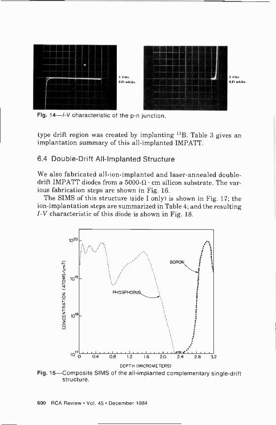
0.01 mA/div.
Fig. 14-I -V characteristic of the p -n junction.
1 v/div.
0.01 mA/dir.
type drift region was created by implanting "B. Table 3 gives an implantation summary of this all -implanted IMPATT.
6.4 Double -Drift All -Implanted Structure
We also fabricated all -ion -implanted and laser -annealed double - drift IMPATT diodes from a 5000-12 cm silicon substrate. The var- ious fabrication steps are shown in Fig. 16.
The SIMS of this structure (side I only) is shown in Fig. 17; the ion -implantation steps are summarized in Table 4; and the resulting I -V characteristic of this diode is shown in Fig. 18.
0.4 0.8 1.2 1.6 20 2.4 2.8 32
DEPTH (MICROMETERS)
Fig. 15-Composite SIMS of the all -implanted complementary single -drift structu re.
600 RCA Review Vol. 45 December 1984
Si mm -WAVE ICs
Table 3-Single-Drift All -Implanted Complementary Structure
Implant No. Side Ion
Equivalent Energy IkeV)
Equivalent Dose
(atoms cm -2)
1 1 B 50 1.54 x 10¹⁵
2 I B 200 1.20 x 10¹²
3 I B 300 1. 21 x 1012
4 I B 400 1.43 x 10¹²
5 II P 1500 3.0 x 10¹⁵
6 II P 1000 1.0 x 10¹⁵
7 II P 400 2.55 x 10¹⁵
8 II P 180 1.26 x 10¹⁵
9 II P 60 6.37 x 10¹⁴
The experiments described in Sections 6.1 to 6.4 clearly demon- strate the feasibility of achieving both p and n layers from high -
resistivity silicon substrates while preserving the bulk high -resis- tivity property of the substrate.
7. p -i -n Diode
Mesa p -i -n diodes were fabricated by means of ion implantation and laser annealing. The various fabrication steps are shown in Fig. 19.
The breakdown voltage exceeds 400 V, and the C -V measurements
(a)
(b)
(c)
ION IMPLANTATION & LASER ANNEALING
////(///,
f f f fl ION IMPLANTATION & LASER ANNEALING
n+CONTACT
n DRIFT REGION
p DRIFT REGION
METALLIZATION - nCONTACT n DRIFT REGION p DRIFT REGION
THINNED SUBSTRATE
METALLIZATION n+ CONTACT
n DRIFT REGION
p DRIFT REGION p+ CONTACT
Fig. 16-Fabrication of the all -implanted double -drift structure.
RCA Review Vol. 45 December 1984 601
1031
1020
io1
ARSENIC AREAL DENSITY -8. 5.101/w3
BORON AREAL DENSITY-
A.
0. 3 a. e A .
0.0 1.2 1.5
DEPTH (micrometers) Fig. 17-SIMS of the double -drift, all -implanted structure.
indicate that full depletion of the i layer occurs at a bias voltage (VB) of -1 V. The C -V characteristics of a typical diode are shown in Table 5 and plotted in Fig. 20.
In fabricating lateral p -i -n diodes, aligned masks were used to first implant the p+ contact and then the n } contact into 5000- (2 cm n -type silicon. The wafers were then annealed, and the metal contacts were defined. The first run was annealed by conventional high -temperature techniques, with a diode breakdown voltage (at
Table 4-Double-Drift All -Implanted Structure
Region Side Ion
Equivalent Energy (keV)
Equivalent Dose (atoms cm')
1 I As 90 3.31x10¹⁴ 2 I As 150 4.93 x 10¹⁴
3 I P 170 9.67 x 10" 4 I P 270 1.49 x 10¹² 5 I P 400 2.55 x 10¹² 6 I B 220 2.96 x 10¹² 7 I B 320 2.45 x 10¹² 8 II B 400 1.00 x 10¹⁵
9 II B 190 2.83 x 10¹⁵ 10 II B 60 1.71 x 10¹⁵
602 RCA Review Vol. 45 December 1984
Si mm -WAVE ICs
f CI 1111
111111111111rommai °
URUR lill1111111111111111ER 1_741_,111189L,
5 V/d iv.
Fig. 18-I -V characteristic of the double -drift, all -implanted structure.
IR = 10 µA) of 700 V. The second run was laser annealed with similar results. Fig. 21 depicts a typical lateral p -i -n diode in a series configuration with a transmission line, ideally a silicon mi- crostrip line.
8. Conclusion
The first SIMMWIC has been successfully fabricated. This circuit is a monolithic SPST switch with a 3 -dB bandwidth of 20% and a minimum isolation of 21.6 dB across the band (center frequency is 36.75 GHz). This monolithic circuit is a low-cost, reproducible foun- dation for all millimeter -wave control applications.
SIMMWIC technology was used to fabricate microstrip-line oscil- lator circuits on silicon, and various types of IMPATT and p -i -n
(a)
METALLIZATION
n -TYPE Si
IMPLANTED AND LASER ANNEALED)
.-METALLIZATION
(b) ////Z////////Z4 +
P
(THINNED SUBSTRATE)
METALLIZATION
(c) ¡ff/77/Y/L! L +
r,///,',/////////75000d1-cm P
IMPLANTED AND siiriirsiiril LASER ANNEALED)
METALLIZATION
Fig. 19-Fabrication of p -i -n diodes by SIM MWIC technology.
RCA Review Vol. 45 December 1984 603
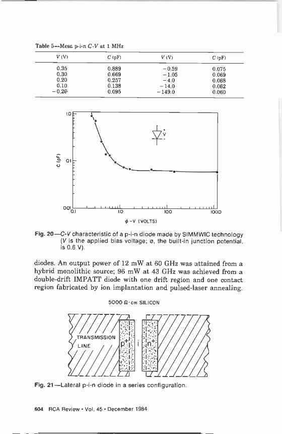
Table 5-Mesa p -i -n C -V at 1 MHz
C (pF)
0.35 0.889 -0.59 0.075 0.30 0.669 -1.05 0.069 0.20 0.257 -4.0 0.068 0.10 0.138 -14.0 0.062
-0.2C- 0.095 -14y.o 0.060
1.0
0.01 01
° °
....../ . .....| . ......| m
ck-v (voLrs)
10.0 100.0
Fig. 20-C -V characteristic of a p -i -n diode made by SIMMWIC technology (V is the applied bias voltage; o, the built-in junction potential, is 0.6 V).
diodes. An output power of 12 mW at 60 GHz was attained from a hybrid monolithi source; 96 mW at 43 GHz was achieved from a double -drift IMPATT diode with one drift region and one contact region fabricated by ion implantation and pulsed -laser annealing.
5000 .0. cm SILICON
TRANSMISSION
LINE
Fig. 21-Lateral p -i -n diode in a series configuration.
604 RCA Review Vol. 4o`December 1984
Si mm -WAVE ICs
Single- and double -drift all -implanted diodes have been made from high -resistivity substrates by ion implantation, laser annealing, and novel wafer thinning. Lateral- and mesa -type p -i -n diodes have also been made by means of this technology. We have demonstrated that SIMMWIC technology is useful for complete millimeter -wave subsystem integration.
Acknowledgments
The authors sincerely appreciate the invaluable contributions of those associated with the SIMMWIC effort at RCA Laboratories: the mechanical expertise of W. M. Janton and S. P. Grober; the pro- cessing skills of A. M. Gombar, K. E. Pinkerton, S. A. Bennett and H. L. Davis; the TEM analysis by J. T. McGinn; the SIMS profile diagnostics of C. W. Magee and E. M. Botnick; the pulsed -laser -an- nealing and ion -implantations expertise of C. P. Wu, F. Kolandra and R. C. Hesser; the expert epitaxial skills of J. F. Corboy and R. H. Pagliaro, Jr.; the technical discussions with P. F. Pelka and A. K. Sharma; and the constant support and encouragement of M.
Nowogrodzki and F. Sterzer. The authors also wish to thank W. J. Lanford and C. Burman of the State University of New York at Albany and S. Manasion of the Fusion Energy Corporation for the high-energy ion implantations.
References:
1 A. Rosen, P. Stabile, J. McGinn, C. Wu, C. Magee, and W. J. Lanford, "Silicon Monolithic Millimeter Wave Sources," Proc. 13th European Microwave Cont., Sept. 1983, pp. 241-246. 2 P. J. Stabile, A. Rosen, W. M. Janton, A. Gonibar, and M. Kolan, "Millimeter Wave Silicon Device and Integrated Circuit Technology," IEEE MTT-S Int. Microwave Symp. Dig., 1984, pp. 448-450. 3 P. J. Stabile, and A. Rosen, "A Silicon Millimeter Wave Integrated Circuit (SIMMWIC) SPST Switch," Electron. Left., 20(22), 943-944 (Oct. 1984).
Texas Instruments MERA Program, 1965. S. G. Liu, C. P. Wu and C. W. Magee, "Annealing of Ion -Implanted GaAs with a
Nd:Class Laser," MP Cont. Proc. No. 50, New York, 1979, p. 603. 6 C. W. Magee, "Depth Profiling of n -Type Dopants in Si and GaAs Using Cs' Bom- bardment Negative Secondary Ion Mass Spectrometry in Ultra -High Vacuum," J.
Electrochem. Soc., 126, 660 (1979). 7 A. G. Cullis, Chapter 6 in Detects in Semiconductors, Ed. by J. Narayan and T. Y.
Tan, North Holland Pub. Co., New York, 1981, p. 393. 8 A. Rosen, M. Caulton, P. Stabile, A. M. Gombar, W. M. Janton, C. P. Wu, J. F.
Corboy, and C. W. Magee, "Millimeter -Wave Devices Technology," IEEE Trans. Mi- crowave Theory Tech., MTT-30(1), 47-55 (1982). 9 A. Rosen, M. Caulton, P. Stabile, A. M. Gombar, W. J. Janton, C. P. Wu, J. F.
Corboy, and C. W. Magee, "Silicon as a Millimeter -Wave Monolithically Integrated Substrate-A New Look," RCA Rev., 42, 633 (Dec. 1981).
RCA Review Vol. 45 December 1984 605
A GaAs Power FET Suitable for Monolithic Integration, with Laser -Processed Gate and Drain Via Connections
R. L. Camisa, G. C. Taylor, F. P. Cuomo, W. F. Reichert, and R. Brown RCA Laboratories, Princeton, NJ 08540
Abstract-A new microwave device format that combines flip -chip and via -connection technologies is described. This approach avoids many of the compromises inherent in conventional mi- crowave monolithic circuits and will be particularly important in power applications. This paper reviews the rationale for this device format and describes a novel method of forming via connections through thick (H < 0.37 mm) semi -insulating sub- strates by a laser -drilling technology.
Preliminary discrete flip -chip devices with gate and drain via connections have been fabricated, and results have been ob- tained through 18 GHz. At 12 GHz, an output power of 308 mW at 28% power -added efficiency and 4.5 -dB power gain have been achieved with a single -cell (0.6 mm/cell) GaAs FET. At 15 GHz, two 0.6 -mm -width cells were lumped -element matched and combined, and an output power of 448 mW was obtained with 19.7% power -added efficiency and 4 -dB gain. Efficiencies as high as 31% were achieved with these preliminary devices.
Introduction
In a conventional monolithic microwave circuit,1 such as that illus- trated in Fig. 1(a), a via connection2 is made between the device source contact and a metal heatsink. This necessitates unavoidable performance compromises because of contradictory substrate -thick- ness requirements. In power applications, a low thermal resistance is necessary to maintain low operating -channel temperature for im-
606 RCA Review Vol. 45 December 1984
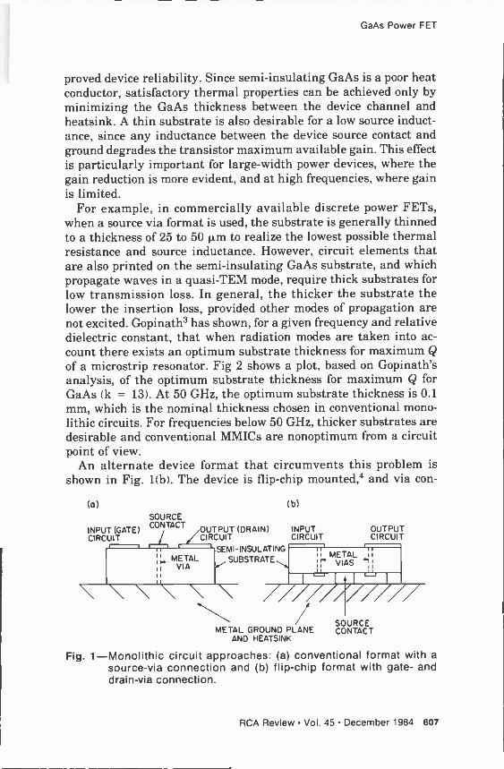
GaAs Power FET
proved device reliability. Since semi -insulating GaAs is a poor heat conductor, satisfactory thermal properties can be achieved only by minimizing the GaAs thickness between the device channel and heatsink. A thin substrate is also desirable for a low source induct- ance, since any inductance between the device source contact and ground degrades the transistor maximum available gain. This effect is particularly important for large -width power devices, where the gain reduction is more evident, and at high frequencies, where gain is limited.
For example, in commercially available discrete power FETs, when a source via format is used, the substrate is generally thinned to a thickness of 25 to 50 p.m to realize the lowest possible thermal resistance and source inductance. However, circuit elements that are also printed on the semi -insulating GaAs substrate, and which propagate waves in a quasi-TEM mode, require thick substrates for low transmission loss. In general, the thicker the substrate the lower the insertion loss, provided other modes of propagation are not excited. Gopinath3 has shown, for a given frequency and relative dielectric constant, that when radiation modes are taken into ac- count there exists an optimum substrate thickness for maximum Q
of a microstrip resonator. Fig 2 shows a plot, based on Gopinath's analysis, of the optimum substrate thickness for maximum Q for GaAs (k = 13). At 50 GHz, the optimum substrate thickness is 0.1 mm, which is the nominal thickness chosen in conventional mono- lithic circuits. For frequencies below 50 GHz, thicker substrates are desirable and conventional MMICs are nonoptimum from a circuit point of view.
An alternate device format that circumvents this problem is shown in Fig. 1(b). The device is flip -chip mounted,4 and via con -
(a)
INPUT (GATE) CIRCUIT
SOURCE CONTACT OUTPUT (DRAIN)
CIRCUIT
SEMI -INSULATING SUBSTRATE
(b)
INPUT CIRCUIT
METAL GROUND PLANE AND HEATSINK
OUTPUT CIRCUIT
SOURCE CONTACT
Fig. 1-Monolithic circuit approaches: (a) conventional format with a
source -via connection and (b) flip -chip format with gate- and drain -via connection.
RCA Review Vol. 45 December 1984 607
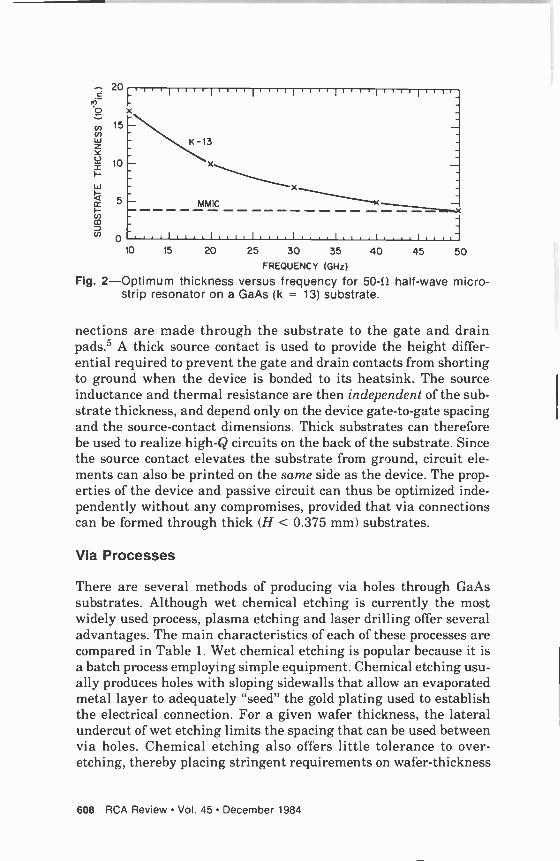
20 ,..r 111111111'1 11111,111, 111
.I1.I1I....I....1.1.e1....1..1.1 10 15 20 25 30 35 40 45 50
FREQUENCY (GHz)
Fig. 2-Optimum thickness versus frequency for 50-9 half -wave micro - strip resonator on a GaAs (k = 13) substrate.
nections are made through the substrate to the gate and drain pads.5 A thick source contact is used to provide the height differ- ential required to prevent the gate and drain contacts from shorting to ground when the device is bonded to its heatsink. The source inductance and thermal resistance are then independent of the sub- strate thickness, and depend only on the device gate -to -gate spacing and the source -contact dimensions. Thick substrates can therefore be used to realize high -Q circuits on the back of the substrate. Since the source contact elevates the substrate from ground, circuit ele- ments can also be printed on the same side as the device. The prop- erties of the device and passive circuit can thus be optimized inde- pendently without any compromises, provided that via connections can be formed through thick (H < 0.375 mm) substrates.
Via Processes
There are several methods of producing via holes through GaAs substrates. Although wet chemical etching is currently the most widely used process, plasma etching and laser drilling offer several advantages. The main characteristics of each of these processes are compared in Table 1. Wet chemical etching is popular because it is a batch process employing simple equipment. Chemical etching usu- ally produces holes with sloping sidewalls that allow an evaporated metal layer to adequately "seed" the gold plating used to establish the electrical connection. For a given wafer thickness, the lateral undercut of wet etching limits the spacing that can be used between via holes. Chemical etching also offers little tolerance to over - etching, thereby placing stringent requirements on wafer -thickness
608 RCA Review Vol. 45 December 1984
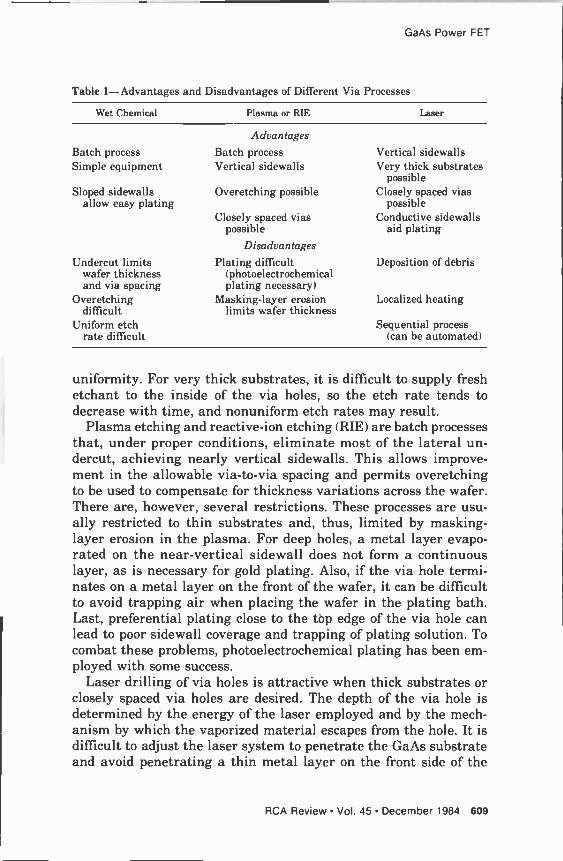
GaAs Power FET
Table 1-Advantages and Disadvantages of Different Via Processes
Wet Chemical Plasma or RIE Laser
Batch process Simple equipment
Sloped sidewalls allow easy plating
Undercut limits wafer thickness and via spacing
Overetching difficult
Uniform etch rate difficult
Advantages
Batch process Vertical sidewalls Vertical sidewalls Very thick substrates
possible Overetching possible Closely spaced vias
possible Closely spaced vias Conductive sidewalls
possible aid plating Disadvantages
Plating difficult Deposition of debris (photoelectrochemical plating necessary)
Masking -layer erosion Localized heating limits wafer thickness
Sequential process (can be automated)
uniformity. For very thick substrates, it is difficult to supply fresh etchant to the inside of the via holes, so the etch rate tends to decrease with time, and nonuniform etch rates may result.
Plasma etching and reactive -ion etching (RIE) are batch processes that, under proper conditions, eliminate most of the lateral un- dercut, achieving nearly vertical sidewalls. This allows improve- ment in the allowable via -to -via spacing and permits overetching to be used to compensate for thickness variations across the wafer. There are, however, several restrictions. These processes are usu- ally restricted to thin substrates and, thus, limited by masking - layer erosion in the plasma. For deep holes, a metal layer evapo- rated on the near -vertical sidewall does not form a continuous layer, as is necessary for gold plating. Also, if the via hole termi- nates on a metal layer on the front of the wafer, it can be difficult to avoid trapping air when placing the wafer in the plating bath. Last, preferential plating close to the top edge of the via hole can lead to poor sidewall coverage and trapping of plating solution. To combat these problems, photoelectrochemical plating has been em- ployed with some success.
Laser drilling of via holes is attractive when thick substrates or closely spaced via holes are desired. The depth of the via hole is determined by the energy of the laser employed and by the mech- anism by which the vaporized material escapes from the hole. It is difficult to adjust the laser system to penetrate the GaAs substrate and avoid penetrating a thin metal layer on the front side of the
RCA Review Vol. 45 December 1984 609
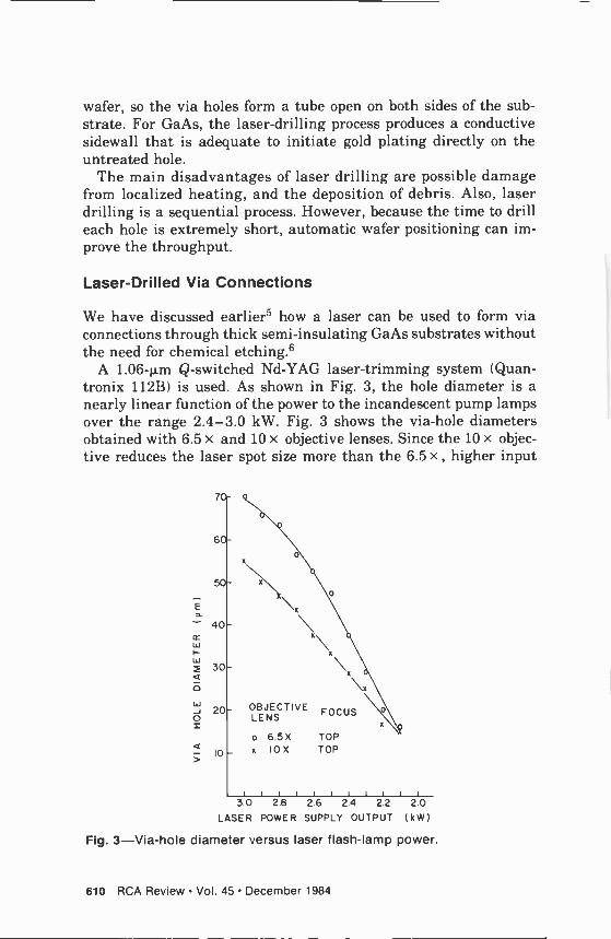
wafer, so the via holes form a tube open on both sides of the sub- strate. For GaAs, the laser -drilling process produces a conductive sidewall that is adequate to initiate gold plating directly on the untreated hole.
The main disadvantages of laser drilling are possible damage from localized heating, and the deposition of debris. Also, laser drilling is a sequential process. However, because the time to drill each hole is extremely short, automatic wafer positioning can im- prove the throughput.
Laser -Drilled Via Connections
We have discussed earlier5 how a laser can be used to form via connections through thick semi -insulating GaAs substrates without the need for chemical etching.6
A 1.06 -p.m Q -switched Nd-YAG laser -trimming system (Quan- tronix 112B) is used. As shown in Fig. 3, the hole diameter is a nearly linear function of the power to the incandescent pump lamps over the range 2.4-3.0 kW. Fig. 3 shows the via -hole diameters obtained with 6.5 x and 10 x objective lenses. Since the 10 x objec- tive reduces the laser spot size more than the 6.5 x higher input
50
E
- 40 cc
F w
30
ó
ó 20 x
10
OBJECTIVE FOCUS LENS
o 6.5X TOP x 10 X TOP
3.0 2.8 2.6 2.4 2.2 2.0
LASER POWER SUPPLY OUTPUT (kW)
Fig. 3-Via-hole diameter versus laser flash -lamp power.
610 RCA Review Vol. 45 December 1984
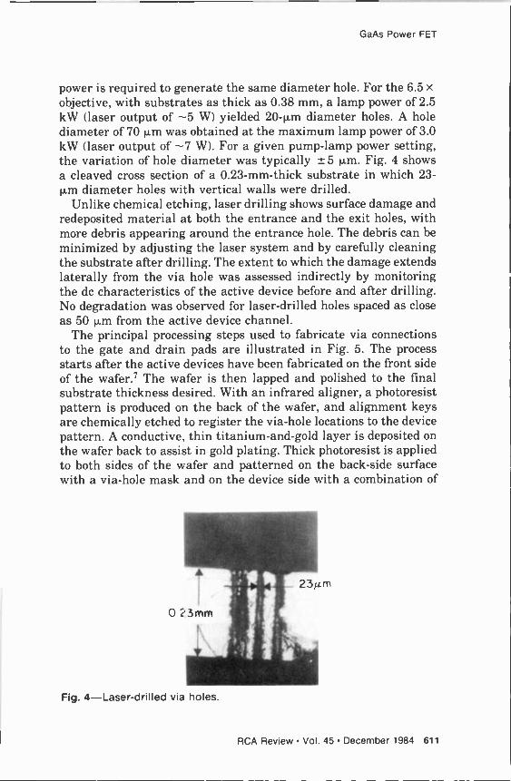
GaAs Power FET
power is required to generate the same diameter hole. For the 6.5 x objective, with substrates as thick as 0.38 mm, a lamp power of 2.5 kW (laser output of -5 W) yielded 20-µm diameter holes. A hole diameter of 70 µm was obtained at the maximum lamp power of 3.0 kW (laser output of -7 W). For a given pump -lamp power setting, the variation of hole diameter was typically ± 5 µm. Fig. 4 shows a cleaved cross section of a 0.23 -mm -thick substrate in which 23- µm diameter holes with vertical walls were drilled.
Unlike chemical etching, laser drilling shows surface damage and redeposited material at both the entrance and the exit holes, with more debris appearing around the entrance hole. The debris can be minimized by adjusting the laser system and by carefully cleaning the substrate after drilling. The extent to which the damage extends laterally from the via hole was assessed indirectly by monitoring the dc characteristics of the active device before and after drilling. No degradation was observed for laser -drilled holes spaced as close as 50 µm from the active device channel.
The principal processing steps used to fabricate via connections to the gate and drain pads are illustrated in Fig. 5. The process starts after the active devices have been fabricated on the front side of the wafer.? The wafer is then lapped and polished to the final substrate thickness desired. With an infrared aligner, a photoresist pattern is produced on the back of the wafer, and alignment keys are chemically etched to register the via -hole locations to the device pattern. A conductive, thin titanium -and -gold layer is deposited on the wafer back to assist in gold plating. Thick photoresist is applied to both sides of the wafer and patterned on the back -side surface with a via -hole mask and on the device side with a combination of
0.23mm
Fig. 4-Laser-drilled via holes.
_ we 11.1, _ 231cm
" É
RCA Review Vol. 45 December 1984 611
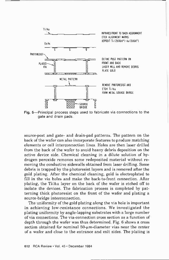
PHOTORESIST
Ti/Au
Go As
S
METAL PATTERN
D
SOURCE
BRIDGE
INFRARED FRONT TO BACK ASSIGNMENT
ETCH ALIGNMENT MARKS
DEPOSIT Ti (2000A°) Au(5O0A°)
DEFINE POST PATTERN ON
FRONT AND BACK
LASER MILL AND REMOVE DEBRIS
PLATE GOLD
REMOVE PHOTORESIST AND
ETCH Ti/Au FORM METAL SOURCE BRIDGE
Fig. 5-Princ pal process steps used to fabricate via connections to the gate and drain pads.
source -post and gate- and drain -pad patterns. The pattern on the back of the wafer can also incorporate features to produce matching elements or cell interconnection lines. Holes are then laser drilled from the back of the wafer to avoid heavy debris deposition on the active device side. Chemical cleaning in a dilute solution of hy- drogen peroxide removes some redeposited material without re- moving the conductive sidewalls obtained from laser drilling. Some debris is trapped by the photoresist layers and is removed after the gold plating. After the chemical cleaning, gold is electroplated to fill in the via holes and make the back-to-front connection. After plating, the Ti/Au layer on the back of the wafer is etched off to isolate the devices. The fabrication process is completed by pat- terning thick photoresist on the front of the wafer and plating a source -bridge interconnection.
The uniformity of the gold plating along the via hole is important in achieving low -resistance connections. We investigated the plating uniformity by angle -lapping substrates with a large number of via connections. The via -connection cross section as a function of depth through the wafer was thus determined. Fig. 6 shows a cross section obtained for nominal 50 -p.m -diameter vias near the center of a wafer and close to the entrance and exit sides. The plating is
612 RCA Review Vol. 45 December 1984
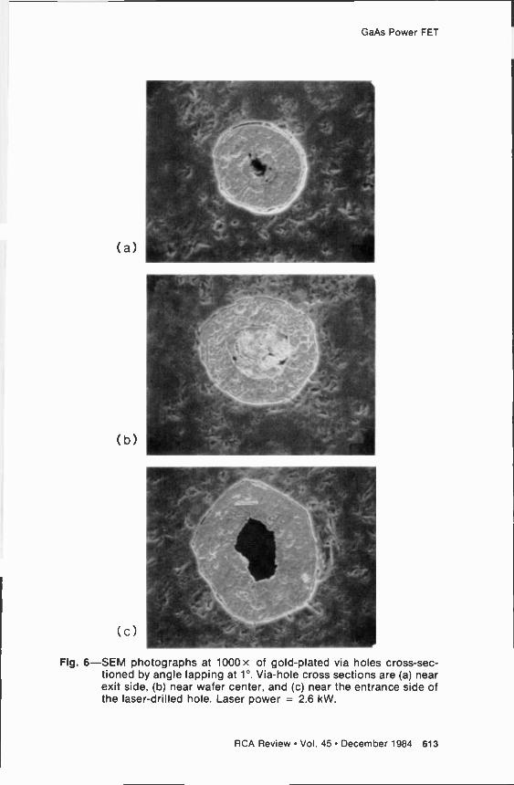
GaAs Power FET
(a)
(b)
(c)
L
Fig. 6-SEM photographs at 1000x of gold-plated via holes cross -sec- tioned by angle lapping at 1°. Via -hole cross sections are (a) near exit side, (b) near wafer center, and (c) near the entrance side of the laser -drilled hole. Laser power = 2.6 kW.
RCA Review Vol. 45 December 1984 613
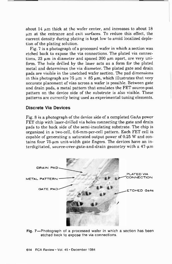
about 14 µm thick at the wafer center, and increases to about 18 µm at the entrance and exit surfaces. To reduce this effect, the current density during plating is kept low to avoid localized deple- tion of the plating solution.
Fig. 7 is a photograph of a processed wafer in which a section was etched back to expose the via connections. The plated via connec- tions, 23 p.m in diameter and spaced 300 p.m apart, are very uni- form. The hole drilled by the laser acts as a form for the plated metal and determines the via diameter. The plated gate and drain pads are visible in the unetched wafer section. The pad dimensions in this photograph are 75 p.m x 85 p.m, which illustrates that very accurate placement of vias across a wafer is possible. Between gate and drain pads, a metal pattern that emulates the FET source -post pattern on the device side of the substrate is also visible. These patterns are currently being used as experimental tuning elements.
Discrete Via Devices
Fig. 8 is a photograph of the device side of a completed GaAs power FET chip with laser -drilled via holes connecting the gate and drain pads to the back side of the semi -insulating substrate. The chip is organized in a two -cell, 0.6 -mm -per -cell pattern. Each FET cell is capable of generating a saturated output power of 0.25 W and con- tains four 75 -p.m unit -width gate fingers. The devices have an in- terdigitated, source -over -gate -and -drain geometry with a 47-µm
DRAIN PAD
PLATED VIA .11,1/../_./ .a.CONNECTION METAL PATTERN/. ' ,
GATE PADr. ''ETCHED GaAs
r -
Fig. 7-Photograph of a processed wafer in which a section has been etched back to expose the via connections.
614 RCA Review Vol. 45 December 1984
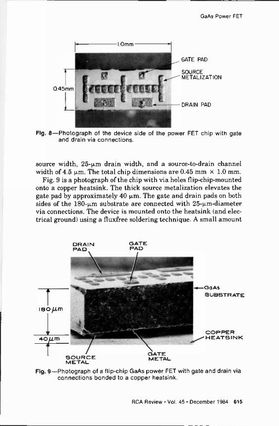
GaAs Power FET
1.Omm
0.45mm
GATE PAD
SOURALIZCE R -METATION
InYak DRAIN PAD
Fig. 8-Photograph of the device side of the power FET chip with gate and drain via connections.
source width, 25-µm drain width, and a source -to -drain channel width of 4.5 p.m. The total chip dimensions are 0.45 mm x 1.0 mm.
Fig. 9 is a photograph of the chip with via holes flip -chip -mounted onto a copper heatsink. The thick source metalization elevates the gate pad by approximately 40 p.m. The gate and drain pads on both sides of the 180 -p.m substrate are connected with 25 -p.m -diameter via connections. The device is mounted onto the heatsink (and elec- trical ground) using a fluxfree soldering technique. A small amount
DRAIN PAD
o
7
GATE PAD
I . f'= .,.
iih.
L K .
SOURCE METAL
Fig. 9-Photograph of a flip -chip GaAs power FET with gate and drain via connections bonded to a copper heatsink.
e-, f-GOAs
. .
;. «Is í
SUBSTRATE
COPPER - HEATSINK
.s ``<
GATE METAL
RCA Review Vol. 45 December 1984 615
of flux is used to flow a solder preform over the metal surface where the FET is to be placed. The flux is then cleaned off, and the device is mechanically placed onto the solder by means of a split -optics flip -chip machine. The chip is fired in a hydrogen atmosphere to reflow the solder, thereby forming a good solder joint between the source bridge and the metal heatsink. While the chip is in the fur- nace, a small weight is used to push it into the solder and assure proper wetting of the entire source -bridge area.
After the source bridge is bonded, ribbons are attached to the gate and drain pads. These ribbons are then connected to external matching circuits. Once the via chip is flipped, the gate and drain pads are readily accessible so that the matching network can be reworked. If a ribbon loosens from the device it can be rewelded or replaced. When a ribbon detaches from a conventional flip -chip de- vice (without vias), the device is lost because all pads are under the chip and cannot be reached.
Performance
The first via devices were evaluated in the 8- to 18-GHz frequency range. These preliminary devices had 5- to 6-V pinchoff voltages. The gate -to -source reverse breakdown voltage was nominally 9 V at a 20-p.A leakage current. The FET drain saturation current was 333 mA/mm, the transconductance 40 mS/mm, and the nominal gate length 0.8 µm. Three different device cell widths (0.15, 0.30, and 0.6 mm) are available on this mask set. The majority of the evaluation was performed on 0.6 -mm -width devices at 12 and 15 GHz.
These devices typically exhibited a maximum unilateral gain (MUG) of 8 dB at 12 GHz and 6 dB at 18 GHz. Power test data are summarized in Table 2. Single -cell 0.6 -mm devices were tuned and tested at discrete frequencies in the 8- to 18-GHz band with external double slug tuners (no internal tuning elements). The input and output standoffs were 0.1-pF capacitors. At 12 GHz, a single 0.6 - mm cell had an output power of 271 mW with 4.3 -dB gain and 25% power -added efficiency. This device, with internal lumped -element matching, had an output power of 308 mW with 4.5 -dB gain and 28% power -added efficiency. When the device was optimized for ef- ficiency, an output power of 231 mW with 5.2 -dB gain and 31% efficiency was measured. At 15 GHz, a lumped -element matched and combined two -cell device had an output power of 448 mW with 4.0 -dB gain and 19.7% efficiency. The results are very encouraging.
616 RCA Review Vol. 45 December 1984
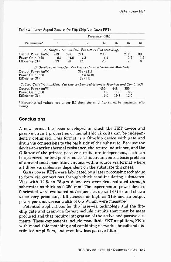
GaAs Power FET
Table 2-Large-Signal Results for Flip -Chip Via GaAs FETs
Performance*
Frequency (GHz)
8 10 12 14 15 16 18
A. Single-(0.6-mm)Cell Via Device (No Matching) Output Power (mW) 253 325 271 230 212 139 Power Gain (dB) 5.1 4.5 4.3 4.1 3.7 3.3 Efficiency (%) 29 26 25 20 17 6
B. Single-(0.6-mm)Cell Via Device (Lumped -Element Matched) Output Power (mW) 308 (231) Power Gain (dB) 4.5 (5.2) Efficiency (%) 28 (31)
C. Two -Cell (0.6-mm/Cell) Via Device (Lumped -Element Matched and Combined) Output Power (mW) 450 448 350 Power Gain (dB) 4.0 4.0 3.2 Efficiency (%) 19.0 19.7 12.0
* Parenthetical values (see under B.) show the amplifier tuned to maximum effi- ciency.
Conclusions
A new format has been developed in which the FET device and passive -circuit properties of monolithic circuits can be indepen- dently optimized. This format is a flip -chip device with gate and drain via connections to the back side of the substrate. Because the device -to -carrier thermal resistance, the source inductance, and the Q factor of the printed passive circuits are independent, each can be optimized for best performance. This circumvents a basic problem of conventional monolithic circuits with a source via format where all three variables are dependent on the substrate thickness.
GaAs power FETs were fabricated by a laser processing technique to form via connections through thick semi -insulating substrates. Vias with 12.5- to 75-µm diameters were demonstrated through substrates as thick as 0.350 mm. The experimental power devices fabricated were evaluated at frequencies up to 18 GHz and shown to be very promising. Efficiencies as high as 31% and an output power per unit device width of 0.5 W/mm were measured.
Potential applications for the laser -via technology and the flip - chip gate and drain -via format include circuits that must be mass produced and that require integration of the active and passive ele- ments. These components include monolithic FET amplifiers, FETs with monolithic matching and combining networks, broadband dis- tributed amplifiers, and even low -loss passive filters.
RCA Review Vol. 45 December 1984 617
Acknowledgment
The authors wish to acknowledge the support of A. Mikelsons, J. Cordas, and E. Mykietyn. Valuable discussions with S. Y. Narayan are also acknowledged gratefully.
References:
1 R. A. Pucel, "Design Considerations for Monolithic Microwave Circuits," IEEE Trans. Microwave Theory Tech., MTT-29(6), p. 513 (June 1981). 2 L. A. D'Asaro, J. V. DiLorenzo, and H. Fukui, "Improved Performance of GaAs Microwave Field Effect Transistors with Via Connections Through the Substrate," IEDM Tech. Dig., pp. 370-371 (Dec. 1977). 3 A. Gopinath, "Maximum Q -Factor of Microstrip Resonators," IEEE Trans. Micro- wave Theory Tech., MTT-29(2), p. 128 (Feb. 1981). 4 I. Drukier, R. L. Camisa, S. T. Jolly, H. C. Huang, and S. Y. Narayan, "Medium Power GaAs Field -Effect Transistors," Electron. Lett., 11(5), p. 104 (March 1975). 5 R. L. Camisa, G. Taylor, W. Reichert, F. Cuomo, and R. Brown, "A Flip -Chip GaAs Power FET with Gate and Drain Via Connections," IEEE Electron Device Lett., EDL- 5(4), p. 118 (April 1984). 6 A. W. Tucker and M. Birnbaum, "Laser Chemical Etching of Vias in GaAs," IEEE Electron Device Lett., EDL-4(2), p. 39 (Feb. 1983).
G. C. Taylor, Y. Yun, S. G. Liu, S. T. Jolly, and D. Bechtle, "GaAs Power Field - Effect Transistors for K -Band Operation," RCA Rev., 42(4), p. 508 (Dec. 1981).
618 RCA Review Vol. 45 December 1984
i
Advances in the Design of Solid -State Power Amplifiers for Satellite Communications*
Brian Dornan, Michael Cummings, and Frank McGinty RCA Laboratories, Princeton, NJ 08540
Abstract-The development of solid-state power amplifiers (SSPAs) to replace traveling -wave -tube amplifiers in satellite communi- cations systems is described. The initial development work, which began in the mid -1970s, was made possible by the de-
velopment of the GaAs FET device. This early development work resulted in a significantly improved communication system; to date, over 100 SSPAs have been included in oper- ating geosynchronous satellites. Operational results for these transponders indicate a significant improvement in channel ca- pacity due in large part to the linearity achievable with SSPAs. In this paper, we discuss the design of and give test results for several advanced SSPAs designed to operate at higher output power (6, 10, and 12 W) than the earlier design.
Introduction
During the past several years, RCA has been involved in the de- velopment of solid-state amplifiers for communication satellites. Part of this involvement resulted in the development of a space - qualified 8.5 -watt amplifier which was launched on the first all - solid -state C -band communication satellite, RCA Satcom 5, in Oct. 1982. Since that time, the design and development of several ad- vanced solid-state C -band amplifiers has been completed.
The initial work focused not only on the rf performance of SSPAs, but also upon such aspects of amplifier design as producibility and
Partial funding for this program has been provided by Intelsat under Contract INTEL -138.
RCA Review Vol. 45 December 1984 619
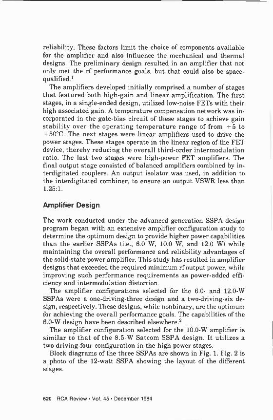
reliability. These factors limit the choice of components available for the amplifier and also influence the mechanical and thermal designs. The preliminary design resulted in an amplifier that not only met the rf performance goals, but that could also be space - qualified.'
The amplifiers developed initially comprised a number of stages that featured both high -gain and linear amplification. The first stages, in a single -ended design, utilized low -noise FETs with their high associated gain. A temperature compensation network was in- corporated in the gate -bias circuit of these stages to achieve gain stability over the operating temperature range of from +5 to + 50°C. The next stages were linear amplifiers used to drive the power stages. These stages operate in the linear region of the FET device, thereby reducing the overall third -order intermodulation ratio. The last two stages were high -power FET amplifiers. The final output stage consisted of balanced amplifiers combined by in- terdigitated couplers. An output isolator was used, in addition to the interdigitated combiner, to ensure an output VSWR less than 1.25:1.
Amplifier Design
The work conducted under the advanced generation SSPA design program began with an extensive amplifier configuration study to determine the optimum design to provide higher power capabilities than the earlier SSPAs (i.e., 6.0 W, 10.0 W, and 12.0 W) while maintaining the overall performance and reliability advantages of the solid-state power amplifier. This study has resulted in amplifier designs that exceeded the required minimum rf output power, while improving such performance requirements as power -added effi- ciency and intermodulation distortion.
The amplifier configurations selected for the 6.0- and 12.0-W SSPAs were a one -driving -three design and a two -driving -six de- sign, respectively. These designs, while nonbinary, are the optimum for achieving the overall performance goals. The capabilities of the 6.0-W design have been described elsewhere.2
The amplifier configuration selected for the 10.0-W amplifier is similar to that of the 8.5-W Satcom SSPA design. It utilizes a two -driving -four configuration in the high -power stages.
Block diagrams of the three SSPAs are shown in Fig. 1. Fig. 2 is a photo of the 12 -watt SSPA showing the layout of the different stages.
620 RCA Review Vol. 45 December 1984
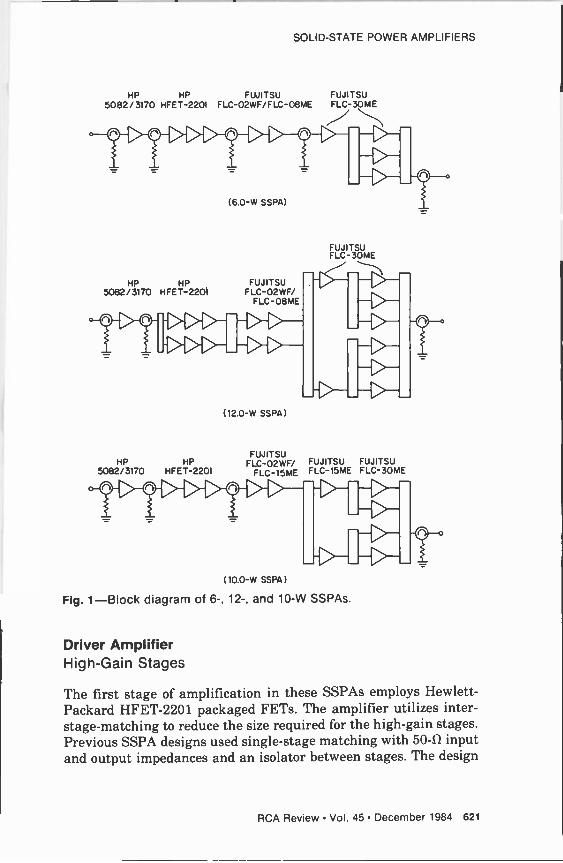
SOLID-STATE POWER AMPLIFIERS
HP HP FUJITSU 5082/3170 HFET-2201 FLC-02WF/FLC-08ME
HP HP 5082/3170 HFET-2201
HP 5082/3170
HP HFET-2201
O
(6.0-W SSPA)
FUJITSU FLC-02WF/
FLC-08ME
(12.0-W SSPA)
FUJITSU FLC-02 WF/
FLC-15ME
>>
(10.0-W SSPA )
FUJITSU FLC-30ME
FUJITSU FLC-30ME
isPg N FUJITSU FUJITSU FLC-15ME FLC-30ME
Fig. 1-Block diagram of 6-, 12-, and 10-W SSPAs.
Driver Amplifier High -Gain Stages
The first stage of amplification in these SSPAs employs Hewlett- Packard HFET-2201 packaged FETs. The amplifier utilizes inter - stage -matching to reduce the size required for the high -gain stages. Previous SSPA designs used single -stage matching with 50-52 input and output impedances and an isolator between stages. The design
RCA Review Vol. 45 December 1984 621
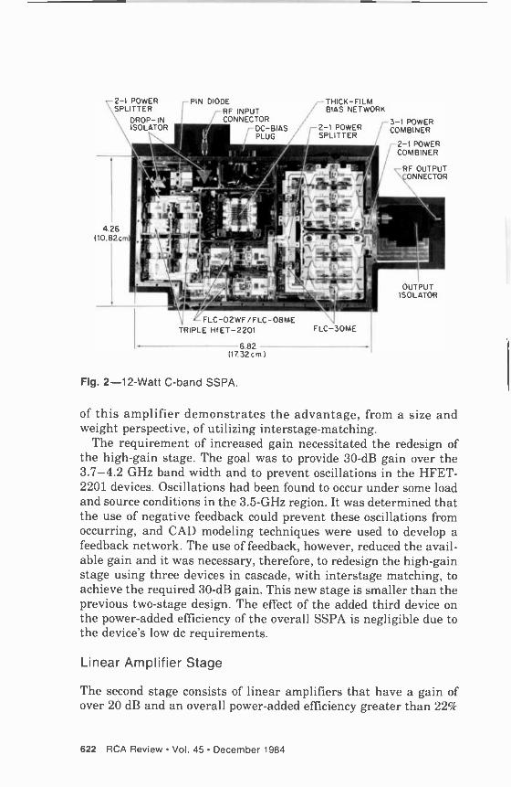
2-1 POWER SPLITTER
,-PIN DIODE r-RF INPUT
DROP-IN / CONNECTOR ISOLATOR
4.26 00.82cm
-
[PLUG
.111 .1:)11
/ PLUG
FLC-02wF/FLC-08ME TRIPLE Hf ET -2201
6.82
THICK-FILM BIAS NETWORK
2-1 POWER SPLITTER
3-1 POW ER COMBINER
2-1 POWER COMBINER
RF OUTPUT ONNECTOR
OUTPUT ISOLATOR
FLC-30ME
07.32cm1
Fig. 2 -12 -Watt C -band SSPA.
of this amplifier demonstrates the advantage, from a size and weight perspective, of utilizing interstage-matching.
The requirement of increased gain necessitated the redesign of the high -gain stage. The goal was to provide 30 -dB gain over the 3.7-4.2 GHz band width and to prevent oscillations in the HFET- 2201 devices. Oscillations had been found to occur under some load and source conditions in the 3.5-GHz region. It was determined that the use of negative feedback could prevent these oscillations from occurring, and CAD modeling techniques were used to develop a feedback network. The use of feedback, however, reduced the avail- able gain and it was necessary, therefore, to redesign the high -gain stage using three devices in cascade, with interstage matching, to achieve the required 30 -dB gain. This new stage is smaller than the previous two -stage design. The effect of the added third device on the power -added efficiency of the overall SSPA is negligible due to the device's low dc requirements.
Linear Amplifier Stage
The second stage consists of linear amplifiers that have a gain of over 20 dB and an overall power -added efficiency greater than 22%
622 RCA Review Vol. 45 December 1984
SOLID-STATE POWER AMPLIFIERS
at an output power of more than 450 mW to drive the power stages. This linear amplifier stage utilizes interstage-matching, as does the high -gain stage, to minimize the size and weight of the overall in-
tegrated amplifier. Proper selection of devices for this stage was necessary to obtain the required output power without serious gain compression. The devices selected were Fujitsu FLC-02WF and FLC-08ME GaAs FETs. These devices are capable of providing output powers of 200 and 630 mW, respectively, at the 1 -dB gain compression point while providing the required power -added effi-
ciency at 4.0 GHz.
Power Stages
The high -power output stages for the three SSPAs are shown in the block diagrams in Fig. 1. All designs use balanced stages to achieve the required output power: the 6.0-W SSPA uses a one -driving -three configuration, the 10.0-W SSPA uses a two -driving -four configura- tion, and the 12.0-W SSPA uses a two -driving -six configuration. Design considerations for each of the amplifier stages are identical regardless of the configuration considered.
In these designs, a single -ended amplifier is used to drive the balanced amplifier stages. Each balanced stage consists of two or
three transistor amplifier circuits combined by quadrature hybrids. The input power is split equally by the input hybrid, and the am- plifier outputs are combined in the output hybrid. Based on the assumption that the FET amplifiers in each arm are reasonably similar, the input and output VSWRs are then determined by the couplers.
The design goals for the power stages were to achieve high rf output with high efficiency and good linearity. The first step in
attaining this goal, as it is for the previous stages, is to measure the S parameters, plot the impedance, and then to design an initial input -matching circuit.
The next step, and the main difference between designing small - and large -signal circuits, is to characterize the device under large - signal input conditions. Since the output impedance of the device is a function of the input power, it is imperative to know the imped-
ance variation exactly, in order to design an output -matching cir- cuit that will provide the required output power.
The equipment used for large -signal modeling is a unique RCA
development called automatic load pu11.3 The load -pull equipment presents a known output impedance to the device while simulta-
RCA Review Vol. 45 December 1984 623
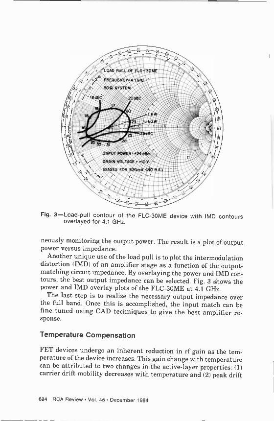
Fig. 3-Load-pull contour of the FLC-30ME device with IMD contours overlayed for 4.1 GHz.
neously monitoring the output power. The result is a plot of output power versus impedance.
Another unique use of the load pull is to plot the intermodulation distortion (IMD) of an amplifier stage as a function of the output - matching circuit impedance. By overlaying the power and IMD con- tours, the best output impedance can be selected. Fig. 3 shows the power and IMD overlay plots of the FLC-30ME at 4.1 GHz.
The last step is to realize the necessary output impedance over the full band. Once this is accomplished, the input match can be fine tuned using CAD techniques to give the best amplifier re- sponse.
Temperature Compensation
FET devices undergo an inherent reduction in rf gain as the tem- perature of the device increases. This gain change with temperature can be attributed to two changes in the active -layer properties: (1) carrier drift mobility decreases with temperature and (2) peak drift
624 RCA Review Vol. 45 December 1984
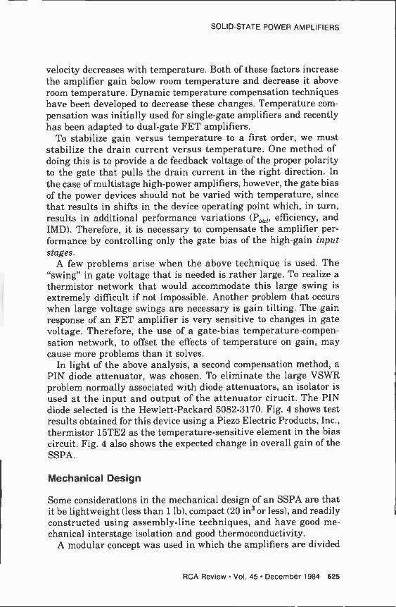
SOLID-STATE POWER AMPLIFIERS
velocity decreases with temperature. Both of these factors increase the amplifier gain below room temperature and decrease it above room temperature. Dynamic temperature compensation techniques have been developed to decrease these changes. Temperature com- pensation was initially used for single -gate amplifiers and recently has been adapted to dual -gate FET amplifiers.
To stabilize gain versus temperature to a first order, we must stabilize the drain current versus temperature. One method of doing this is to provide a dc feedback voltage of the proper polarity to the gate that pulls the drain current in the right direction. In the case of multistage high -power amplifiers, however, the gate bias of the power devices should not be varied with temperature, since that results in shifts in the device operating point which, in turn, results in additional performance variations (Pour, efficiency, and IMD). Therefore, it is necessary to compensate the amplifier per- formance by controlling only the gate bias of the high -gain input stages.
A few problems arise when the above technique is used. The "swing" in gate voltage that is needed is rather large. To realize a thermistor network that would accommodate this large swing is extremely difficult if not impossible. Another problem that occurs when large voltage swings are necessary is gain tilting. The gain response of an FET amplifier is very sensitive to changes in gate voltage. Therefore, the use of a gate -bias temperature -compen- sation network, to offset the effects of temperature on gain, may cause more problems than it solves.
In light of the above analysis, a second compensation method, a PIN diode attenuator, was chosen. To eliminate the large VSWR problem normally associated with diode attenuators, an isolator is used at the input and output of the attenuator cirucit. The PIN diode selected is the Hewlett-Packard 5082-3170. Fig. 4 shows test results obtained for this device using a Piezo Electric Products, Inc., thermistor 15TE2 as the temperature -sensitive element in the bias circuit. Fig. 4 also shows the expected change in overall gain of the SSPA.
Mechanical Design
Some considerations in the mechanical design of an SSPA are that it be lightweight (less than 1 lb), compact (20 in3 or less), and readily constructed using assembly -line techniques, and have good me- chanical interstage isolation and good thermoconductivity.
A modular concept was used in which the amplifiers are divided
RCA Review Vol. 45 December 1984 625
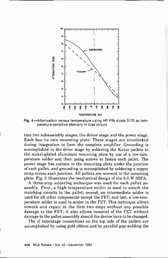
10. rrrTrrri 1....1.... ir¡^TTr^ rrn rrtrrr¡rrrrI I7y . \
r.
4.
1..
MEASURED
N N N N
THEORY
, '....1....1....I....I....I..j.l....l....l..i
la 1
R1
1
ñÍ+ a d11 á 1
TEMPERATURE (C)
h
Fig. 4-Attenuation versus temperature using HP PIN diode 3170 as tem- perature -sensitive element in bias circuit.
into two subassembly stages, the driver stage and the power stage. Each has its own mounting plate. These stages are interlocked during integration to form the complete amplifier. Grounding is accomplished in the drive stage by soldering the Kovar pallets to the nickel -plated aluminum mounting plate by use of a low -tem- perature solder and then using screws to fasten each pallet. The power stage has cutouts in the mounting plate under the junction of each pallet, and grounding is accomplished by soldering a copper strap across each junction. All pallets are screwed to the mounting plate. Fig. 5 -illustrates the mechanical design of the 6.0-W SSPA.
A three -step soldering technique was used for each pallet as- sembly. First, a high -temperature solder is used to attach the matching circuits to the pallet; second, an intermediate solder is used for all other components except the FET; and last, a low -tem- perature solder is used to solder in the FET. This technique allows rework and repair at the first two steps without any possible damage to the FET; it also allows removal of the FET without damage to the pallet assembly should the device have to be changed.
The rf interstage connections on the top side of the pallets are accomplished by using gold ribbon and by parallel gap -welding the
626 RCA Review Vol. 45 December 1984
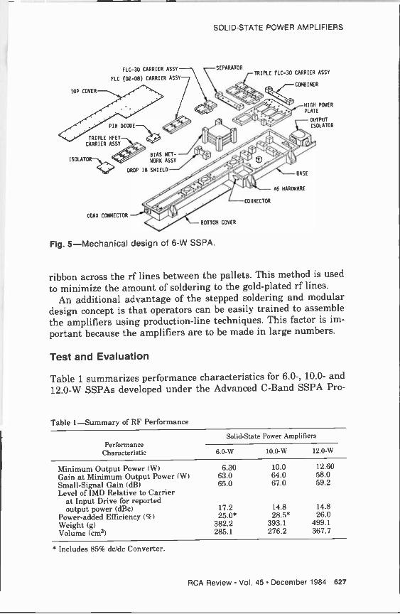
SOLID-STATE POWER AMPLIFIERS
FLC-30 CARRIER ASSY SEPARATOR
FLC (02-08) CARRIER ASSY
TOP COYER
PIN DIODE
TRIPLE HFET CARRIER ASSY
ISOLATOR BIAS NET-
WORK ASSY
DROP IN SHIELD
COAX CONNECTOR
BOTTOM COYER
Fig. 5-Mechanical design of 6-W SSPA.
TRIPLE FLC-30 CARRIER ASSY
CONNECTOR
COMBINER
HIGH POWER PLATE
OUTPUT ISOLATOR
BASE
/6 HARDWARE
ribbon across the rf lines between the pallets. This method is used
to minimize the amount of soldering to the gold-plated rf lines. An additional advantage of the stepped soldering and modular
design concept is that operators can be easily trained to assemble the amplifiers using production -line techniques. This factor is im-
portant because the amplifiers are to be made in large numbers.
Test and Evaluation
Table 1 summarizes performance characteristics for 6.0-, 10.0- and 12.0-W SSPAs developed under the Advanced C -Band SSPA Pro -
Table 1-Summary of RF Performance
Performance Characteristic
Solid -State Power Amplifiers
6.0-W1' 10.0-W 12.0-W
Minimum Output Power (W) 6.30 10.0 12.60 Gain at Minimum Output Power (W) 63.0 64.0 58.0 Small -Signa Gain (dB) 65.0 67.0 59.2 Level of IMD Relative to Carrier
at Input Drive for reported output power (dBc) 17.2 14.8 14.8
Power -added Efficiency (%) 25.0* 28.5* 26.0 Weight (g) 382.2 393.1 499.1 Volume (cm3) 285.1 276.2 367.7
* Includes 85% dc/dc Converter.
RCA Review Vol. 45 December 1984 627
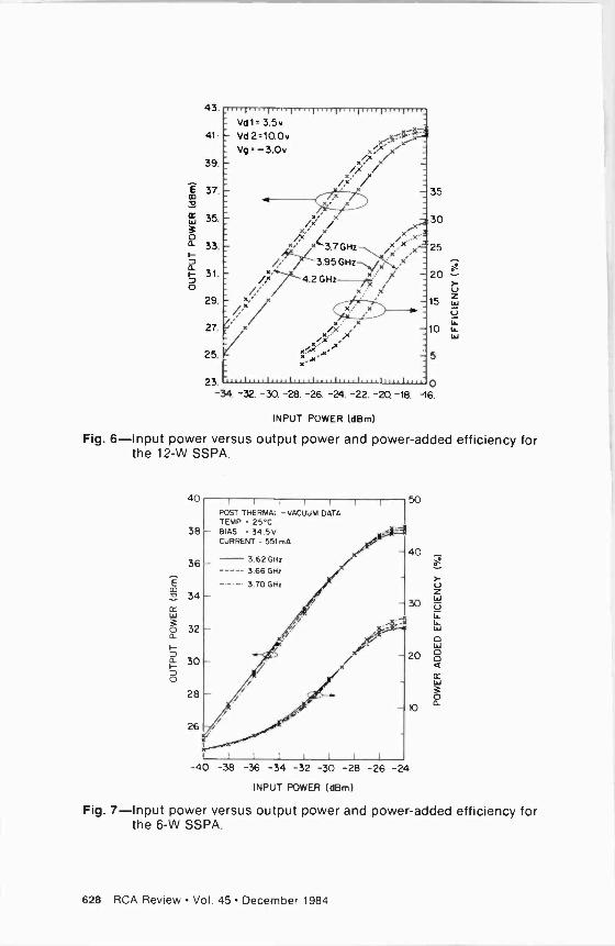
43.
41
39.
m 37.
W 35.
0 a 33. I-
a 31.
ó 29.
27.
25.
23.
....1, Ft 11..,.1. 1111.,,11I11I 1.11..,1 I I
Vd1=3.5v Vd 2=10.0v Vp = - 3.0 v x i x
x x/.x /,."/ //' -35 97/5
30 /x x x; x/ ..; x!. 3.7GHz :.x x-'25 3.95 x -20
4.2 GHz--A -15
-10 /.: /.x
x a -5 -1,,. L 11,1..,,1,1,11111,11 u 111,11I,,111 Ilk : o
-34. -32. -30 -28. -26. -24. -22. -2Q -18. -16.
INPUT POWER (dBm)
Fig. 6-Input power versus output power and power -added efficiency for the 12-W SSPA.
40 POST THERMAL - VACUUM DATA TEMP = 25°C
38 BIAS = 34.5V CURRENT = 551 mA
36
34
32
30
28
3.62 GH:
----- 3.66 GH:
---- 3.70 GM:
40
30
111«
20 x
b
26
t I t I
-40 -38 -36 -34 -32 -30 -28 -26 -24
INPUT POWER (dBm)
Fig. 7-Input power versus output power and power -added efficiency for the 6-W SSPA.
628 RCA Review Vol. 45 December 1984
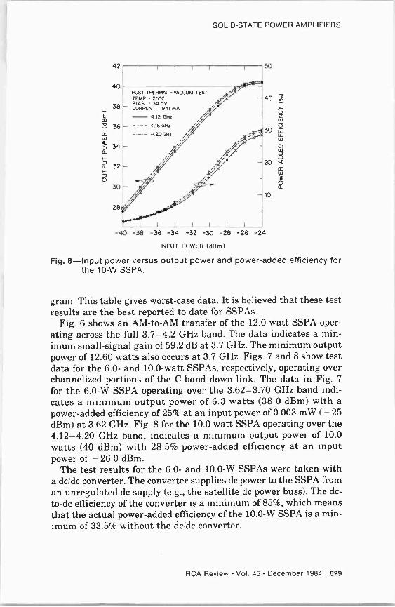
SOLID-STATE POWER AMPLIFIERS
42
40
38
36
34
32
30
8
POST THERMAL -VACUUM TEST TEMP = 25C BIAS = 34.5V >k/ CURRENT = 941 mA >f%z - 4.12 GHz i - - - - 4.16 GHz
- -- 4.20 GHz
-40 -38 -36 -34 -32 -30 -28
INPUT POWER (dBm)
40
30
20
10
-26 -24
Fig. 8-Input power versus output power and power -added efficiency for the 10-W SSPA.
gram. This table gives worst -case data. It is believed that these test results are the best reported to date for SSPAs.
Fig. 6 shows an AM -to -AM transfer of the 12.0 watt SSPA oper- ating across the full 3.7-4.2 GHz band. The data indicates a min- imum small -signal gain of 59.2 dB at 3.7 GHz. The minimum output power of 12.60 watts also occurs at 3.7 GHz. Figs. 7 and 8 show test data for the 6.0- and 10.0 -watt SSPAs, respectively, operating over channelized portions of the C -band down -link. The data in Fig. 7
for the 6.0-W SSPA operating over the 3.62-3.70 GHz band indi- cates a minimum output power of 6.3 watts (38.0 dBm) with a power -added efficiency of 25% at an input power of 0.003 mW (- 25 dBm) at 3.62 GHz. Fig. 8 for the 10.0 watt SSPA operating over the 4.12-4.20 GHz band, indicates a minimum output power of 10.0 watts (40 dBm) with 28.5% power -added efficiency at an input power of - 26.0 dBm.
The test results for the 6.0- and 10.0-W SSPAs were taken with a dc/dc converter. The converter supplies dc power to the SSPA from an unregulated dc supply (e.g., the satellite dc power buss). The dc -
to -dc efficiency of the converter is a minimum of 85%, which means that the actual power -added efficiency of the 10.0-W SSPA is a min- imum of 33.5% without the dc/dc converter.
RCA Review Vol. 45 December 1984 629
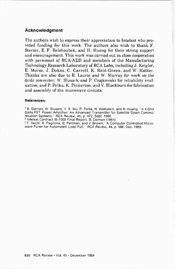
Acknowledgment
The authors wish to express their appreciation to Intelsat who pro- vided funding for this work. The authors also wish to thank F. Sterzer, E. F. Belohoubek, and H. Huang for their strong support and encouragement. This work was carried out in close cooperation with personnel of RCA/AED and members of the Manufacturing Technology Research Laboratory of RCA Labs, including J. Keigler, E. Morse, J. Dokas, C. Carroll, K. Reid -Green, and W. Hatter. Thanks are also due to R. Laurie and W. Murray for work on the dc/dc converter; W. Slusark and P. Czajkowski for reliability eval- uation; and P. Pelka, K. Pinkerton, and V. Blackburn for fabrication and assembly of the microwave circuits.
References:
1 B. Dornan, W. Slusark, Y. S. Wu, P. Pelka, H. Wolkstein, and H. Huang, "A 4-GHz GaAs FET Power Amplifier: An Advanced Transmitter for Satellite Down Commu- nication Systems," RCA Review, 41, p. 472, Sept. 1980. 2lntelsat Contract IS -1000 Final Report, B. Dornan (1981). 3 F. Sechi, R. Paglione, B. Perlman, and J. Brown, "A Computer Controlled Micro- wave Tuner for Automated Load Pull," RCA Review, 44, p. 566, Dec. 1983.
630 RCA Review Vol. 45 December 1984
Communication Receivers for Satellites --A Review
H. B. Goldberg and S. S. Dhillon RCA Astro -Electronics, Princeton, NJ 08540
Abstract-This paper reports the development of all solid-state low -noise wideband receivers for use in communication and direct - broadcast satellites operating in the 5.9- to 6.4-GHz, 14.0- to 14.5-GHz, and 17.3- to 17.8-GHz uplink frequency bands. The receivers provide low -noise and spurious free down conversion of the uplink frequency bands to the downlink frequency bands of 3.7 to 4.2 GHz, 11.7 to 12.2 GHz, and 12.2 to 12.7 GHz, re-
spectively, with excellent frequency stability. The receivers in- corporate state-of-the-art GaAs FET devices and microwave in- tegrated -circuit technologies. Details of the design and mea- sured performance of receivers are given.
Introduction
Astro -Electronics has been designing and building communications satellites since the early 1970s, but not until 1978 did AE begin to design the microwave hardware used in the communication -system transponders. One of the first microwave subsystems to be designed and put into production is the 6/4-GHz communications receiver. This unit is a wide -bandwidth receiver covering the full communi- cation spectrum assigned to the satellite, and it amplifies all of the signals of a transponder simultaneously. Since then, 14/12-GHz and 17/12-GHz communication receivers have also been developed and put into production.1-3
The 6/4-GHz receiver is used on C -band communication tran- sponders. Its input band (uplink) is 5.925 to 6.425 GHz, and its output band (downlink) is 3.7 to 4.2 GHz. The 14/12-GHz receiver is used on the Ku -band commercial communication satellites. Its uplink is 14.0 to 14.5 GHz, and its downlink, 11.7 to 12.2 GHz. The
RCA Review Vol. 45 December 1984. 631
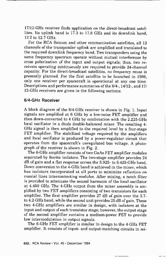
17/12-GHz receiver finds application on the direct -broadcast satel- lites. Its uplink band is 17.3 to 17.8 GHz and its downlink band, 12.2 to 12.7 GHz.
For the RCA Satcom and other communication satellites, all 12 channels of the transponder uplink are amplified and translated to the required downlink frequency band. Two transponders using the same frequency spectrum operate without mutual interference by cross polarization of the input and output signals; thus, two re- ceivers operating continuously are required to provide 24 -channel capacity. For the direct -broadcast satellites, no frequency reuse is presently planned. For the first satellite to be launched in 1986, only one receiver per spacecraft is operational at any one time. Descriptions and performance summaries of the 6/4-, 14/12-, and 17/ 12-GHz receivers are given in the following sections.
6/4-GHz Receiver
A block diagram of the 6/4-GHz receiver is shown in Fig. 1. Input signals are amplified at 6 GHz by a low -noise FET amplifier and then down -converted to 4 GHz by combination with the 2.225-GHz local oscillator in a diode double -balanced mixer. The resulting 4- GHz signal is then amplified to the required level by a four -stage FET amplifier. The stabilized voltage required by the amplifiers and local oscillator is produced by a power -regulator circuit that operates from the spacecraft's unregulated bus voltage. A photo- graph of the receiver is shown in Fig. 2.
The 6-GHz amplifier consists of two GaAs FET amplifier modules separated by ferrite isolators. The two -stage amplifier provides 24 dB of gain and a flat response across the 5.925- to 6.425-GHz band. Down conversion to the 4-GHz band is achieved in the mixer, which has isolators incorporated at all ports to minimize reflection on coaxial lines interconnecting modules. After mixing, a notch filter is provided to attenuate the second harmonic of the local oscillator at 4.450 GHz. The 4-GHz output from the mixer assembly is am- plified by two FET amplifiers consisting of two transistors for each amplifier. The first amplifier provides 27 dB of gain over the 3.7 - to 4.2-GHz band, while the second unit provides 25 dB of gain. These two 4-GHz amplifiers are similar in design, with isolators at the input and output of each transistor stage; however, the output stage of the second amplifier contains a medium -power FET to provide low intermodulation in output signals.
The 6-GHz FET amplifier is similar in design to the 4-GHz FET amplifier. It consists of input- and output -matching circuits in mi -
632. RCA Review Vol. 45 December 1984
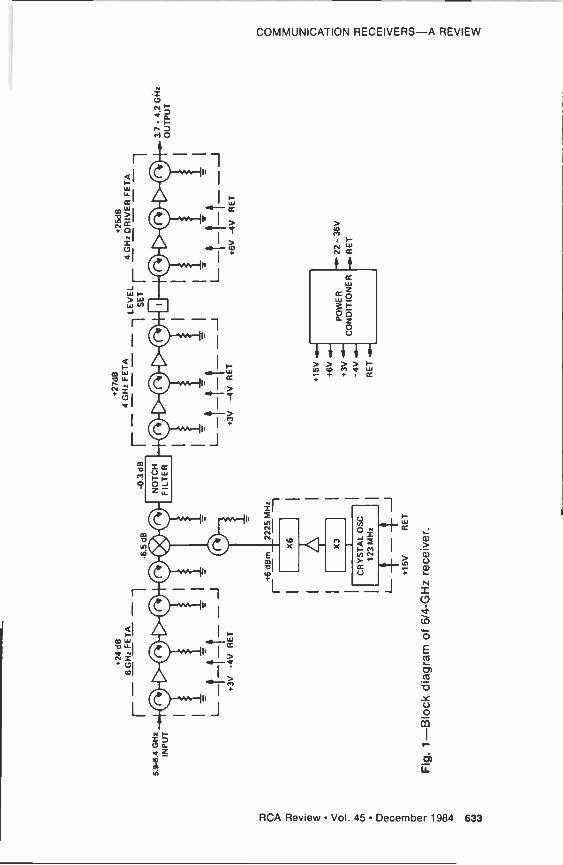
COMMUNICATION RECEIVERS-A REVIEW
CO W O W n H fV =
L
J
Lf) +
C. Q ¢
r f N
RCA Review Vol. 45 December 1984 633
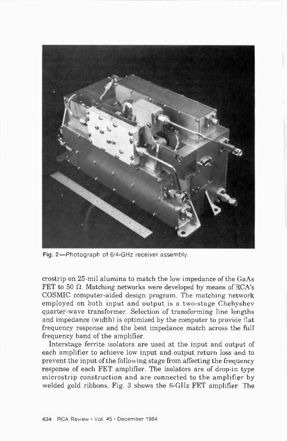
11
Fig. 2-Photograph of 6/4-GHz receiver assembly.
crostrip on 25 -mil alumina to match the low impedance of the GaAs FET to 50 1Z. Matching networks were developed by means of RCA's COSMIC computer -aided design program. The matching network employed on both input and output is a two -stage Chebyshev quarter -wave transformer. Selection of transforming line lengths and impedance (width) is optimized by the computer to provide flat frequency response and the best impedance match across the full frequency band of the amplifier.
Interstage ferrite isolators are used at the input and output of each amplifier to achieve low input and output return loss and to prevent the input of the following stage from affecting the frequency response of each FET amplifier. The isolators are of drop -in type microstrip construction and are connected to the amplifier by welded gold ribbons. Fig. 3 shows the 6-GHz FET amplifier. The
634 RCA Review Vol. 45 December 1984
COMMUNICATION RECEIVERS-A REVIEW
eti + \ l i , + I t 1
;ti:f ié\.' 11:.° f\
amn .-
" _
4 334 , + + 1 .234 , i I r i
+e ,ri:.n.+'rs,rir4 sn+i'-;I T1, 4 ú
It t
Fig. 3-Photograph of 6-GHz amplifier assembly.
two FET amplifiers with input- and output -matching networks on
alumina substrates are mounted on Kovar* carriers and drop into the chassis; the isolators are soldered directly to the chassis.
The 6/4-GHz receiver operates over a temperature range of -7 to + 55°C. The uncompensated FET amplifier will show a drop in
gain at high temperatures and an increase in gain at low temper- atures. To offset this effect and hold the gain constant, the current in the transistor can be increased at high temperatures, and de-
creased at low temperatures. Thís ís done by varying the gate bias of each FET by means of a simple voltage -divider circuit containing a temperature -sensitive component and resistors. The temperature - sensitive component is a sensistor with a positive temperature coef-
ficient that causes the FET current to increase at high temperatures and decrease at low temperatures. The resistors in the circuit set the gate voltage and linearize the temperature -compensating effect of the sensistor. By proper component selection, the uncompensated gain change can be reduced by a factor of 3 to 5, depending on
transistor type and initial operating current. The local oscillator consists of a crystal oscillator at 123.611 MHz,
multipliers, amplifiers, and filters to generate a signal at 2.225 GHz. Each module is designed to work into a 50-12 impedance and is tuned up and tested in test fixtures before assembly in the local
oscillator housing, as shown in Fig. 4.
Reg. trademark of Carpenter Steel. Kovar steel is an alloy having a thermal coef- ficient of expansion close to that of alumina.
RCA Review Vol. 45 December 1984 635
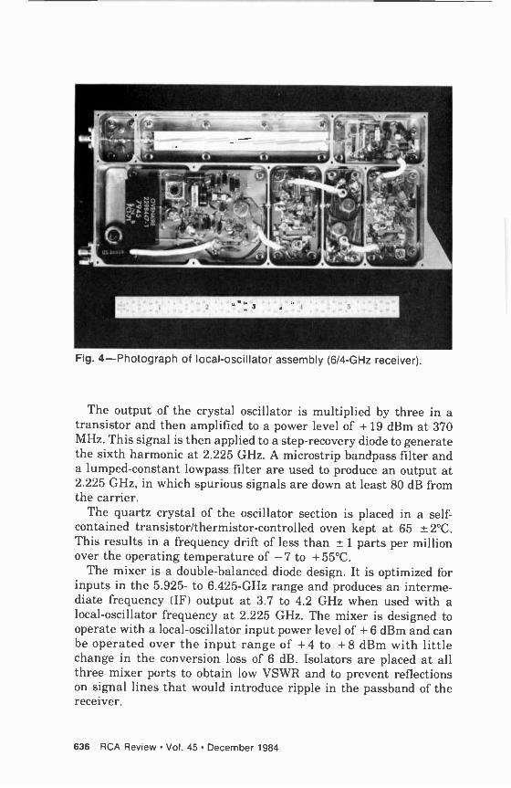
_.l -1ti,, ---®i- , -_, _ _. - -frs . ,5Z11.
11
-
o
e
- 9 I ,,' * »
&ImS ' %:. >z _. _ , 5.`"' III
I, os aww
]
o f C
Fig. 4-Photograph of local -oscillator assembly (6/4-GHz receiver).
The output of the crystal oscillator is multiplied by three in a transistor and then amplified to a power level of + 19 dBm at 370 MHz. This signal is then applied to a step -recovery diode to generate the sixth harmonic at 2.225 GHz. A microstrip bandpass filter and a lumped -constant lowpass filter are used to produce an output at 2.225 GHz, in which spurious signals are down at least 80 dB from the carrier.
The quartz crystal of the oscillator section is placed in a self- contained transistor/thermistor-controlled oven kept at 65 ±2°C. This results in a frequency drift of less than ± 1 parts per million over the operating temperature of -7 to + 55°C.
The mixer is a double -balanced diode design. It is optimized for inputs in the 5.925- to 6.425-GHz range and produces an interme- diate frequency (IF) output at 3.7 to 4.2 GHz when used with a local -oscillator frequency at 2.225 GHz. The mixer is designed to operate with a local -oscillator input power level of +6 dBm and can be operated over the input range of +4 to +8 dBm with little change in the conversion loss of 6 dB. Isolators are placed at all three mixer ports to obtain low VSWR and to prevent reflections on signal lines that would introduce ripple in the passband of the receiver.
636 RCA Review Vol. 45 December 1984
COMMUNICATION RECEIVERS-A REVIEW
The notch filter is to reduce the level of the second harmonic (4.45 GHz) of the local oscillator, which is generated by the mixing pro- cess, by at least 30 dB. To this end, a two -pole filter is required. It consists of two quarter -wavelength resonators, short-circuited at one end and open -circuited at the other, that are proximity -coupled to the main transmission line.
Filter tuning is accomplished with capacitive -loading tuning screws located on the side covers of the filter. The tuning screws adjust the end -effect loading at the open end of the quarter -wave- length resonant lines, as well as the capacitive coupling between the resonant lines and the main transmission line. The center fre- quency of the notch is tuned to 4.448 GHz (12 MHz below 4.450 GHz) to account for a frequency shift when the receiver is operated in a vacuum.
Test Results for the 6/4-GHz Receiver
Extensive testing is performed on each receiver to verify that it meets all performance specifications. Testing starts at the module level, with each FET module being tested to demonstrate gain and flat response across the band and in the temperature range of -7 to +55°C. Modules are then placed in a chassis, tuned, and retested at the subassembly level.
The same testing process is repeated on the local -oscillator printed -circuit boards so that each is aligned in a test fixture. After all subassemblies are tested, they are assembled into the receiver chassis; the completed receiver FET amplifiers are then fine tuned with gold tabs on the alumina substrate to equalize the gain so that variations in gain across the 500 -MHz band are no more than about 0.5 dB. Receiver gain is set to 60 dB by placing a fixed attenuator pad into the 4-GHz FET amplifier chain. A series of temperature tests are performed to measure gain at hot and cold temperatures. Fig. 5 shows the gain of a typical receiver at - 7, + 27, and + 45°C, in which the gain -adjust attenuator pad had been selected to put the receiver gain in the range of 59 to 61 dB over the temperature range. A receiver -noise figure of 3.0 dB is typical at ambient tem- perature across the 500 -MHz frequency band. At + 45°C an increase of 0.2 dB in the noise figure can be expected.
In addition to the bench and thermal tests, the receiver is sub- jected to vibration in three planes and to several days of operation in a thermal vacuum to verify performance in a simulated space environment.
RCA Review Vol. 45 December 1984 637
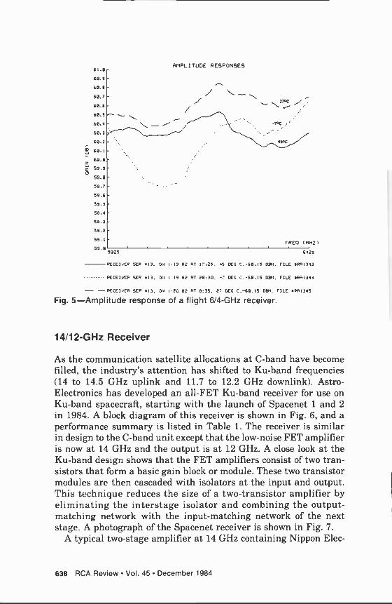
61.0
60.9
60.0
60.7
60.6
60.5
60.4
60.3
60.2
60.1
60.0
59.9
59.6
59.7
59.6
59.5
59.4
59.3
59.2
59.1
59.0
AMPLITUDE RESPONSES
\ ' // ...\... \:111111_,/
FECEIVEF SEP
RECEIVER SCP
-RECEIVED SEP
45PC
FRED (MHz)
6425
13. 014 PI, 82 RT 17,25, 45 DEG C.-60.15 00M. FILE 4681343
*13. ON 1:19 $2 R7 20:30. -7 DEG :.-60.15 DBM, FILE 681344
13, ON 1.20 02 R7 0:35, 27 DEG C,-60.15 0911, FILE PR1345
Fig. 5 -Amplitude response of a flight 6/4-GHz receiver.
14/12-GHz Receiver
As the communication satellite allocations at C -band have become filled, the industry's attention has shifted to Ku -band frequencies (14 to 14.5 GHz uplink and 11.7 to 12.2 GHz downlink). Astro - Electronics has developed an all-FET Ku -band receiver for use on Ku -band spacecraft, starting with the launch of Spacenet 1 and 2
in 1984. A block diagram of this receiver is shown in Fig. 6, and a performance summary is listed in Table 1. The receiver is similar in design to the C -band unit except that the low -noise FET amplifier is now at 14 GHz and the output is at 12 GHz. A close look at the Ku -band design shows that the FET amplifiers consist of two tran- sistors that form a basic gain block or module. These two transistor modules are then cascaded with isolators at the input and output. This technique reduces the size of a two -transistor amplifier by eliminating the interstage isolator and combining the output - matching network with the input -matching network of the next stage. A photograph of the Spacenet receiver is shown in Fig. 7.
A typical two -stage amplifier at 14 GHz containing Nippon Elec-
638 RCA Review Vol. 45 December 1984
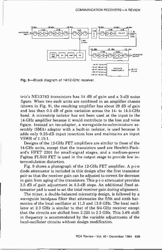
COMMUNICATION RECEIVERS-A REVIEW
-77 dBm
WAVEGUIDE - INPUT
SBdem -46dB
7 0E1 2.3 OH:
56 dBm
-4V AT IOmA
lv AT 170mA
6V AT IOOmA
15VAT55mA 16V AT 145 6144
Fig. 6-Block diagram of 14/12-GHz receiver.
-47 d0m -16 dBm 14 dB -4dB
-7 dB 10111 AT T
WAVEGUIDE OUTPUT
O6 VAT 233 TA
tric's NE13783 transistors has 14 dB of gain and a 3 -dB noise figure. When two such units are combined in an amplifier chassis (shown in Fig. 8), the resulting amplifier has about 28 dB of gain and less than 0.5 dB of gain variation across the 14- to 14.5-GHz band. A microstrip isolator has not been used at the input to the 14-GHz amplifier because it would contribute to the loss and noise figure. Instead an iso-adapter, a waveguide-to-subminiature as- sembly (SMA) adaptor with a built-in isolator, is used because it adds only 0.25 -dB input insertion loss and maintains an input VSWR of 1.15:1.
Designs of the 12-GHz FET amplifiers are similar to those of the 14-GHz units, except that the transistors used are Hewlett-Pack- ard's HFET 2201 for small -signal stages, and a medium -power Fujitsu FLX03 FET is used in the output stage to provide low in- termodulation distortion.
Fig. 9 shows a photograph of the 12-GHz FET amplifier. A p -i -n diode attenuator is included in this design after the first transistor pair so that the receiver gain can be adjusted to correct for decrease in gain from aging of the transistors. This p -i -n attenuator provides 3.5 dB of gain adjustment in 0.5 -dB steps. An additional fixed at- tenuator pad is used to set the total receiver gain during alignment.
The mixer, a double -balanced microstrip design, is followed by a waveguide bandpass filter that attenuates the fifth and sixth har- monics of the local oscillator at 11.5 and 13.6 GHz. The local oscil- lator at 2.3 GHz is similar to that of the 6/4-GHz receiver except that the circuits are shifted from 2.225 to 2.3 GHz. This 3.4% shift in frequency is accommodated by the variable adjustments of the local -oscillator circuits without design modification.
RCA Review Vol. 45 December 1984 639
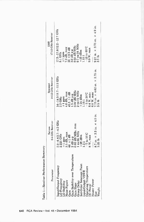
Tab
le 1
-Rec
eive
r Pe
rfor
man
ce S
umm
ary
Para
met
er
Satc
om
6/4-
GH
z R
ecei
ver
Spac
enet
14
/12-
GH
z R
ecei
ver
DB
S 17
/12-
GH
z R
ecei
ver
Inpu
t/Out
put
Freq
uenc
y L
O F
requ
ency
L
O S
tabi
lity
Noi
se F
igur
e G
ain
Gai
n St
abili
ty o
ver
Tem
pera
ture
G
ain
Slop
e G
roup
Del
ay
3rd -
Ord
er I
nter
cept
Poi
nt
Inpu
t/Out
put
VSW
R
Ope
ratin
g T
empe
ratu
re
DC
Po
wer
H
eate
r Po
wer
Si
ze
Wei
ght
5.9-
6.4/
3.7-
4.2
GH
z 2.
225
GH
z ±
1 pp
m
3.5
dB,
max
60
-±
-1 dB
2
dB p
-p
0.02
dB
/MH
z, m
ax
1 ns
/36
MH
z +
28 d
Bm
1.
2:1
-7 to
55°
C
8 W
, m
ax
8.7
in.
x 3.
3 in
. x
4.5
in.
3.25
lb
14-1
4.5/
11.7
-12.
2 G
Hz
2.3
GH
z ±
1 pp
m
4.8
dB,
max
45
.5
± 1
dB
1.
5 dB
p -p
0.
02 d
B/M
Hz
2 ns
/72
MH
z +
24 d
Bm
1.
15:1
-5
to 5
0°C
8.
4 W
, m
ax
6.6
W,
max
7.
75 i
n. x
4.
62 i
n.
x 5.
75 i
n.
3.5
lb
17.3
-17.
8/12
.2-1
2.7
GH
z 5.
1 G
Hz
-±1
ppm
7.
3 dB
, m
ax
35 ±
0.5
dB
3.0
dB p
-p
0.02
dB
MH
z 0.
7 ns
/24
MH
z +
25 d
Bm
1.
15:1
-1
0 to
60°
C
9.0
W,
max
9.27
in
. x
3.75
in.
x
4.9
in.
3.5
lb
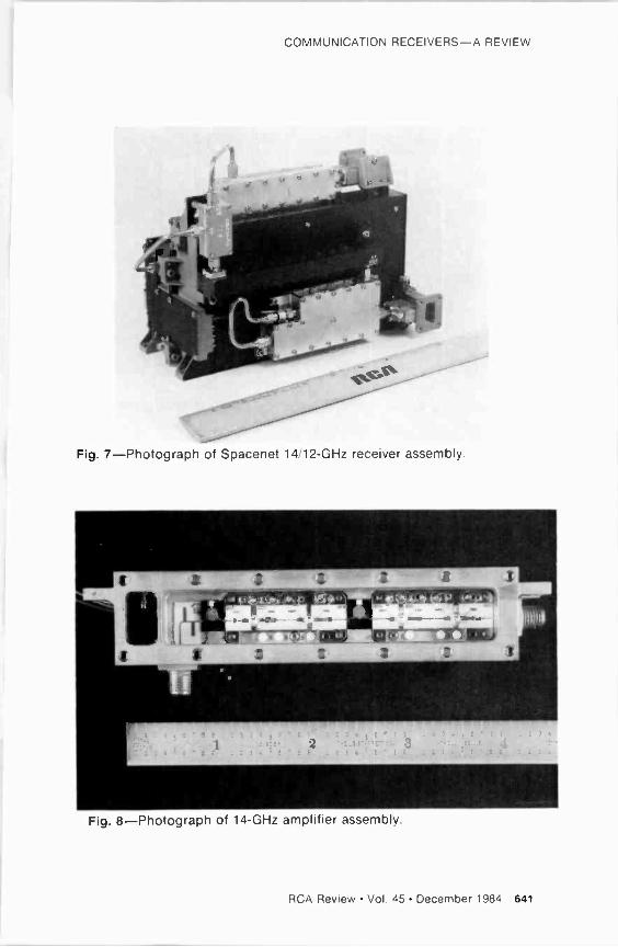
COMMUNICATION RECEIVERS-A REVIEW
d tl
a
e
Fig. 7-Photograph of Spacenet 14/12-GHz receiver assembly.
) i s .., WIV-P-22"IP ke4+ tif--telshwia l
. " ;r--'- J ~^..." 9-.1.
1 ! ¢v_f . +
3
-31 - S '
- . - . . . . . - .
- - -
2 = 3
Fig. 8-Photograph of 14-GHz amplifier assembly.
RCA Review Vol. 45 December 1984 641
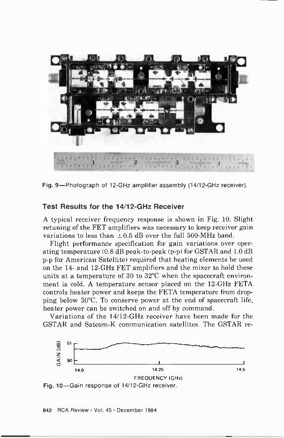
( © 14C .511,51 . a
.
; ' .-= uiu,
_ L.
,r. j ,, Ot II: 1). :; _} w---^ ll lJ r ... .. 9 M " 1 ' 35 _ - . !
.;- :' 4 i r` _.
,,,,,_9 Ia,+z , ..
- 2 e 4 E' e i` I J 4 a 4-! 9 - e e e. 4 ,e 9 . 7 7 4. 6, 9 2 4 i3 4 .6 i ...-C,3-1Y1'..6I '4.93959ce' 2 .76,i,eR:C 3 e'0..14e&D.9A 4 -E-.,:i::.1
1 i 4= 4, e 1
'
2: + e? e e . -- 4 S e- e, - í 3 4' el; 1:. 4 e e+ , i .- u . r .. . . . a
.
..
Fig. 9-Photograph of 12-GHz amplifier assembly (14/12-GHz receiver).
Test Results for the 14/12-GHz Receiver
A typical receiver frequency response is shown in Fig. 10. Slight retuning of the FET amplifiers was necessary to keep receiver gain variations to less than ±0.5 dB over the full 500 -MHz band.
Flight performance specification for gain variations over oper- ating temperature (0.8 dB peak -to -peak (p -p) for GSTAR and 1.0 dB p -p for American Satellite) required that heating elements be used on the 14- and 12-GHz FET amplifiers and the mixer to hold these units at a temperature of 30 to 32°C when the spacecraft environ- ment is cold. A temperature sensor placed on the 12-GHz FETA controls heater power and keeps the FETA temperature from drop- ping below 30°C. To conserve power at the end of spacecraft life, heater power can be switched on and off by command.
Variations of the 14/12-GHz receiver have been made for the GSTAR and Satcom-K communication satellites. The GSTAR re-
m 51
2 Q 50 C7
11.0 14.25
FREQUENCY (GHz)
Fig. 10-Gain response of 14/12-GHz receiver.
14.5
642 RCA Review Vol. 45 December 1984
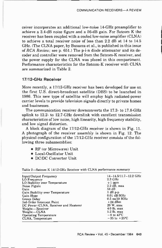
COMMUNICATION RECEIVERS-A REVIEW
ceiver incorporates an additional low -noise 14-GHz preamplifier to achieve a 3.4 -dB noise figure and a 56 -dB gain. For Satcom K the receiver has been coupled with a cooled low -noise amplifier (CLNA) to achieve a total receiver noise of less than 2.2 dB at 14 to 14.5 GHz. (The CLNA paper, by Busacca et al., is published in this issue of RCA Review; see p. 651.) The p -i -n diode attenuator and its de- coder and controller were removed from the Satcom-K receiver, and the power supply for the CLNA was placed in this compartment. Performance characteristics for the Satcom-K receiver with CLNA are summarized in Table 2.
17/12-GHz Receiver
More recently, a 17/12-GHz receiver has been developed for use on the first U.S. direct -broadcast satellite (DBS) to be launched in 1986. This new type of satellite will employ high radiated -power carrier levels to provide television signals directly to private homes and businesses.
The communication receiver downconverts the 17.3- to 17.8-GHz uplink to 12.2- to 12.7-GHz downlink with excellent transmission characteristics of low noise, high linearity, high frequency stability, and low signal distortion.
A block diagram of the 17/12-GHz receiver is shown in Fig. 11. A photograph of the receiver assembly is shown in Fig. 12. The physical configuration of the 17/12-GHz receiver consists of the fol- lowing three subassemblies:
RF (or Microwave) Unit Local -Oscillator Unit DC/DC Converter Unit
Table 2-Satcom K 14/12-GHz Receiver with CLNA performance summary
Input/Output Frequency 14-14.5/11.7-12.2 GHz LO Frequency 2.3 GHz LO Stability over Temperature ±1 ppm Noise Figure 2.2 dB, max Gain 58 dB Gain Stability over Temperature 1 dB p -p Gain Slope 0.01 dB/MHz Group Delay 0.5 ns/30 MHz 3rd -Order Intercept Point +24 dBm DC Power (CLNA, Receiver and Heaters) 20 W, max Weight-Receiver 4.0 Ib, max Weight-CLNA 1.2 1b, max Operating Temperature -8 to 43°C CLNA, Temperature -35 to +25°C
RCA Review Vol. 45 December 1984 643
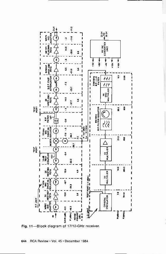
R F
. U
NIT
r- -
T - _
,,,,e
- -
- - -
-
I 17
G
els
1 I
14 d
B
71-I
WR62
1
20
I W
C
( 2X
I
TE
ST
CL
I
ISO
- I
NE
673e
31
DR
OP
-IN
I N
E67
363
(CO
UP
LE
sl)
N
,AD
AP
TE
RI
FE
TA
'IS
OLA
TO
RI
FE
TA
'
w
li 1'O
, O
O"O
, JO
3
I i 1
1
i O
M
GA
IN 0
:1B
) (1
-0.3
I
12.0
1
-n7
I 12
0 I
V
P (
dBrn
(1-1
6.3
' I
-316
(
I-21
3 I
I 1
1 I
N
FIG
UR
E'-
NO
ISE
'
11
I I
to
1
+íi
dej
---1
--1-
-1 -
2 : (
11:1
'c
25C
L
--
N
(D
O
fD
G
0)
TE
ST
P
OR
T
NIT
T
ES
T P
OR
T (
-1 d
am(
CR
YS
TA
L O
SC
ILLA
TO
R
'
NO
B/N
I 7.
0 I
F(M
Hz)
11
4.44
I
L --
--`
03
MU
LTIP
LIE
R
I -3
.4
( O
, a.0
-.S
I 12
Wiz
1
I M
IC
I D
RO
P -IN
M
IXE
R I
ISO
LAT
OR
1
-337
2a
7 I
7.5
I
1 --
1--
P 0.7 d
arn
Lo
=
S.1
W
iz
B. P
.
FIL
TE
R
-10
TE
ST
P
OR
T
I
I 1
ax
I S
ING
LE
, 1
NE
177/
I
WR
75
I I
HF
ET
-220
1 I
S.O
.T. C
HIP
H
FE
T.2
201
FLX
03M
B I
1S0-
I
I I
FETA
1
AT
TE
NU
AT
OR
I F
ET
A
1
'
FETA
IADAPTER
101
I O
O
I I O
1 1 e-
OU
T
1 I
, I
1
14.0
f
-7.3
ls
1-
.S
: 14
.0I
I
I
1
-23.
7 -5
1.0
I (
-XO
1
-11.
0 I-
11.3
I
I I
I (
I I
I 13
I
' 6.
0 '
` I
1
----
1--
-- ..... .
...o
....
... J
14.0
2113
03
MU
LTIP
LIE
R
B.P
. F
ILT
ER
IS
OLA
TO
R
I
21.5
sso
I
1 51
00 M
Hz
1
150
MH
z I
B.P
. +
L.
P.
I F
ILT
ER
20.0
I
1 1
eso
5100
I
, 1 ( J
06
SR
D
MU
L T
IPLI
ER
I
ti 1V
/11,
ti
+3V
+6V
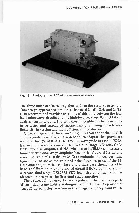
COMMUNICATION RECEIVERS-A REVIEW
A' . 4 S .,
.s ti 4 9 e, 4 1 4 4 4 Y
I
4 4 4.`
4 4 4 5yg- t
4 4 4
4 4 t, v
4 P
4 4 4 Y
\ V
4 4 V
Y'ó.t:
C 7
J h¡ ki7
Fig. 12-Photograph of 17/12-GHz receiver assembly.
The three units are bolted together to form the receiver assembly. This design approach is similar to that used for 6/4-GHz and 14/12- GHz receivers and provides excellent rf shielding between the low- level microwave circuits and the high-level local oscillator (LO) and do/dc converter circuits. It also makes it possible for the three units to be tested and assembled independently, allowing considerable flexibility in testing and high efficiency in production.
A block diagram of the rf unit (Fig. 11) shows that the 17-GHz input signals pass through a wideband iso-adaptor that provides a well -matched (VSWR , 1.15:1) WR62 waveguide-to-coaxial(SMA) transition. The signals are coupled to a dual -stage NE67383 GaAs FET low -noise amplifier (LNA) via a coaxial(SMA)-to-microstrip launcher. The dual -stage amplifier has a noise figure of 3.8 dB and a nominal gain of 12.0 dB (at 25°C) to maintain the receiver noise figure. Fig. 13 shows the gain and noise -figure response of the 17-
GHz dual -stage amplifier. The signals then pass through a wide - band 17-GHz microwave -integrated -circuit (MIC) drop -in isolator to a second dual -stage NE67383 FET low -noise amplifier, which is identical in design to the first dual -stage amplifier.
The do decoupling networks on the gain and the drain bias ports of each dual -stage LNA are designed and optimized to provide at least 25 -dB bandstop rejection in the image frequency band (7.1 to
RCA Review Vol. 45 December 1984 645
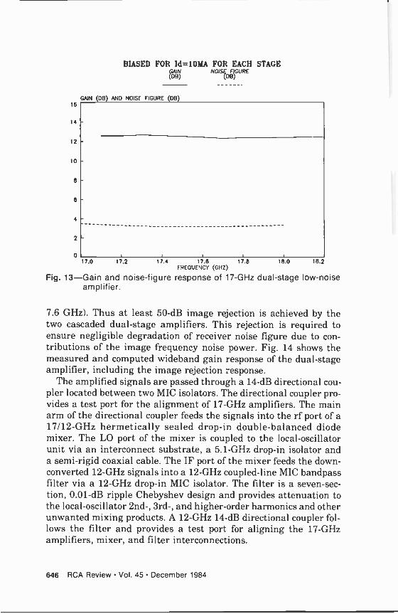
16
14
12
10
e
e
4
2
0
BIASED FOR Id=10MA FOR EACH STAGE CAB; NOislp firRE
GAIN (DB) AND NOISE FIGURE (DB)
---------------------------------------------------
17.0 17.2 17.4 17.6 17.8 18.0 18.2 FNEOUEIICY (WIZ)
Fig. 13-Gain and noise -figure response of 17-GHz dual -stage low -noise amplifier.
7.6 GHz). Thus at least 50 -dB image rejection is achieved by the two cascaded dual -stage amplifiers. This rejection is required to ensure negligible degradation of receiver noise figure due to con- tributions of the image frequency noise power. Fig. 14 shows the measured and computed wideband gain response of the dual -stage amplifier, including the image rejection response.
The amplified signals are passed through a 14 -dB directional cou- pler located between two MIC isolators. The directional coupler pro- vides a test port for the alignment of 17-GHz amplifiers. The main arm of the directional coupler feeds the signals into the rf port of a 17/12-GHz hermetically sealed drop -in double -balanced diode mixer. The LO port of the mixer is coupled to the local -oscillator unit via an interconnect substrate, a 5.1-GHz drop -in isolator and a semi -rigid coaxial cable. The IF port of the mixer feeds the down - converted 12-GHz signals into a 12-GHz coupled -line MIC bandpass filter via a 12-GHz drop -in MIC isolator. The filter is a seven -sec- tion, 0.01 -dB ripple Chebyshev design and provides attenuation to the local -oscillator 2nd-, 3rd-, and higher -order harmonics and other unwanted mixing products. A 12-GHz 14 -dB directional coupler fol- lows the filter and provides a test port for aligning the 17-GHz amplifiers, mixer, and filter interconnections.
646 RCA Review Vol. 45 December 1984
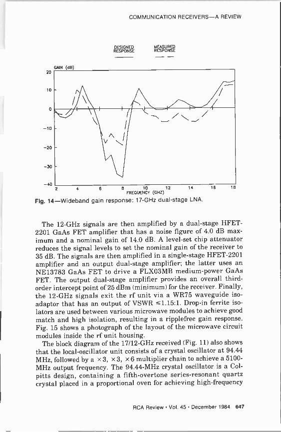
COMMUNICATION RECEIVERS-A REVIEW
20
10
-10
-20
- 30
- 40
DESIGNED MEASURED RESPONSE RESPONSE
GAIN (dB)
/ \ 2 4 6 8 10 12 14 16 18
FREQUENCY (GHZ)
Fig. 14-Wideband gain response: 17-GHz dual -stage LNA.
The 12-GHz signals are then amplified by a dual -stage HFET- 2201 GaAs FET amplifier that has a noise figure of 4.0 dB max- imum and a nominal gain of 14.0 dB. A level -set chip attenuator reduces the signal levels to set the nominal gain of the receiver to 35 dB. The signals are then amplified in a single -stage HFET-2201 amplifier and an output dual -stage amplifier; the latter uses an NE13783 GaAs FET to drive a FLX03MB medium -power GaAs FET. The output dual -stage amplifier provides an overall third - order intercept point of 25 dBm (minimum) for the receiver. Finally, the 12-GHz signals exit the rf unit via a WR75 waveguide iso-
adaptor that has an output of VSWR 1.15:1. Drop -in ferrite iso-
lators are used between various microwave modules to achieve good
match and high isolation, resulting in a ripplefree gain response. Fig. 15 shows a photograph of the layout of the microwave circuit modules inside the rf unit housing.
The block diagram of the 17/12-GHz received (Fig. 11) also shows that the local -oscillator unit consists of a crystal oscillator at 94.44 MHz, followed by a x 3, x 3, x 6 multiplier chain to achieve a 5100 -
MHz output frequency. The 94.44 -MHz crystal oscillator is a Col-
pitts design, containing a fifth -overtone series -resonant quartz crystal placed in a proportional oven for achieving high -frequency
RCA Review Vol. 45 December 1984 647

3
Fig. 15-Photograph of the rf unit (17/12-GHz receiver).
stability over life and temperature. The first x 3 multiplier uses a bipolar -transistor biased Class A but overdriven to form square - wave signals at its output. A double -tuned circuit in the collector provides the load impedance at the third harmonic (283.3 MHz) for power transfer and attenuates the unwanted harmonics. The mul- tiplier has a saturated output power of 14 dBm and drives a second x 3 multiplier that is similarly designed. The second x 3 multiplier feeds the output at 850 MHz into a tuned amplifier that provides saturated output of 21.5 dBm. The amplified output is then filtered by a four -section 850 -MHz combline bandpass filter to suppress the unwanted harmonics. A low -loss isolator couples the signal into a x 6 step -recovery diode (SRD) multiplier. The SRD multiplier pro- vides an output of 11.5 dBm at 5.1 GHz. A MIC bandpass/low-pass filter combination follows the x 6 multiplier. The filters reject the unwanted harmonics of 850 MHz to provide a clean 5.1-GHz signal with an output power level of 9 dBm at the LO output port. All of the LO circuits are housed inside a compact housing. Fig. 16 shows the layout of the rf circuits inside the local -oscillator unit.
Test Results for the 17/12-GHz Receiver
A development model receiver was integrated, aligned, and tested
648 RCA Review Vol. 45 December 1984
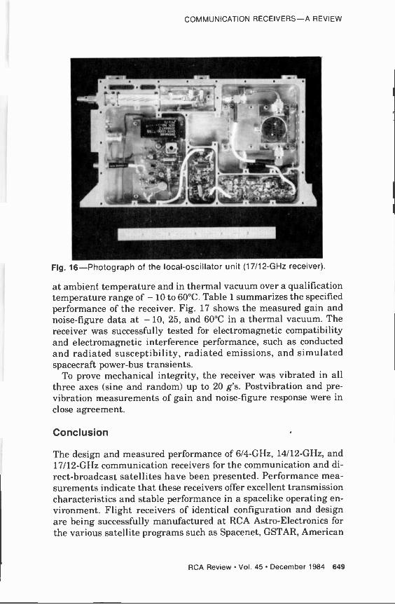
COMMUNICATION RECEIVERS-A REVIEW
, .5?
~..ws-
.VON I-.
"'
z
_ 5
.
r , . ; _(-J4V4. ,.. .
_ .
Fig. 16-Photograph of the local -oscillator unit (17/12-GHz receiver).
at ambient temperature and in thermal vacuum over a qualification temperature range of -10 to 60°C. Table 1 summarizes the specified performance of the receiver. Fig. 17 shows the measured gain and noise -figure data at -10, 25, and 60°C in a thermal vacuum. The receiver was successfully tested for electromagnetic compatibility and electromagnetic interference performance, such as conducted and radiated susceptibility, radiated emissions, and simulated spacecraft power -bus transients.
To prove mechanical integrity, the receiver was vibrated in all three axes (sine and random) up to 20 g's. Postvibration and pre - vibration measurements of gain and noise -figure response were in close agreement.
Conclusion
The design and measured performance of 6/4-GHz, 14/12-GHz, and 17/12-GHz communication receivers for the communication and di- rect -broadcast satellites have been presented. Performance mea- surements indicate that these receivers offer excellent transmission characteristics and stable performance in a spacelike operating en- vironment. Flight receivers of identical configuration and design are being successfully manufactured at RCA Astro -Electronics for the various satellite programs such as Spacenet, GSTAR, American
RCA Review Vol. 45 December 1984 649
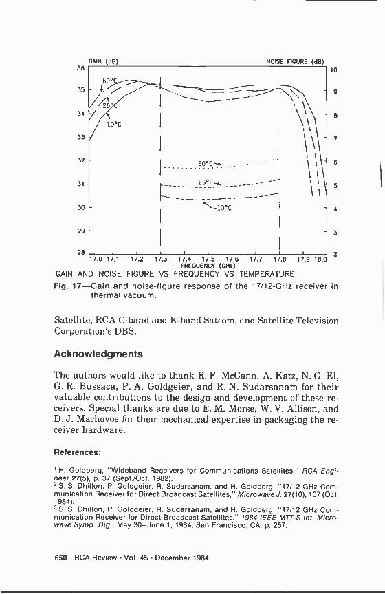
GAIN (dB) 36
35
34
33
32
31
30
29
NOISE FIGURE (dB)
........ .............I
t 25°t:,., -"1 -------------------"
28 1
17.0 17.1 17.2 17.3 17.4 17.5 17.6 17.7 17.8 17.9 18.0 FREQUENCY (GHz)
GAIN AND NOISE FIGURE VS FREQUENCY VS TEMPERATURE
Fig. 17-Gain and noise -figure response of the 17/12-GHz receiver in thermal vacuum.
10
Satellite, RCA C -band and K -band Satcom, and Satellite Television Corporation's DBS.
Acknowledgments
The authors would like to thank R. F. McCann, A. Katz, N. G. El, G. R. Bussaca, P. A. Goldgeier, and R. N. Sudarsanam for their valuable contributions to the design and development of these re- ceivers. Special thanks are due to E. M. Morse, W. V. Allison, and D. J. Machovoe for their mechanical expertise in packaging the re- ceiver hardware.
References:
1 H. Goldberg, "Wideband Receivers for Communications Satellites," RCA Engi- neer 27(5), p. 37 (Sept./Oct. 1982). 2 S. S. Dhillon, P. Goldgeier, R. Sudarsanam, and H. Goldberg, "17/12 GHz Com- munication Receiver for Direct Broadcast Satellites," Microwave J. 27(10), 107 (Oct. 1984). 3 S. S. Dhillon, P. Goldgeier, R. Sudarsanam, and H. Goldberg, "17/12 GHz Com- munication Receiver for Direct Broadcast Satellites," 1984 IEEE MTT-S Int. Micro- wave Symp. Dig., May 30-June 1, 1984, San Francisco, CA, p. 257.
650 RCA Review Vol. 45 December 1984
A 14-GHz Cooled Low -Noise GaAs FET Amplifier for Communication Satellite Application
G. R. Busacca, P. A. Goldgeier, H. B. Goldberg, M. Noyes, and A. Chuchra RCA Astro -Electronics, Princeton, NJ 08540
Abstract-Low-Noise parametric amplifiers have been used in satellite transponders operating at Ku band to produce overall system noise of less than 2.2 dB. Recent advances in GaAs FETs have made it feasible to produce amplifiers using these devices with performance levels approaching those of parametric ampli- fiers. To achieve the required low noise levels, the GaAs FET5 must be cooled. A 14-GHz cooled low -noise amplifier (CLNA) is described, whose design is based on compromises between electrical, thermal, and mechanical design principles. Elec- trical design consisted of rf and power -supply development. RF design involved characterizing and matching GaAs FETs, and cooling required a power supply for the cooler (thermo- electric Peltier junction device) that maintains the amplifier at -50°C. Thermal design consisted of characterizing the heat load of the amplifier, specifying the cooler, and determining an appropriate location on the spacecraft. The mechanical de- sign consisted of developing structural components that are compatible with the mechanical, thermal, and rf environments. Plastic waveguides were developed that serve as low -loss rf transmission mediums and thermal isolators. The engineering model described in this paper has a maximum noise figure, when cooled, of 2.1 dB, a minimum gain of 15.0 dB, and re-
quired 5.0 W of dc power to maintain this performance.
Introduction
Communication satellite transponders must be capable of sensitive signal detection because of the large amount of attenuation present in the uplink path to geosynchronous orbits. Ultralow-noise am -
RCA Review Vol. 45 December 1984 651
plifiers are used on the front end of these transponders to establish the required sensitivity. Parametric amplifiers have previously been used at Ku band to achieve transponder noise figures of less than 2.2 dB.' Parametric amplifiers are sensitive and complex de- vices, however, and are difficult to adapt to the spacecraft environ- ment.
Recent advances in the field of GaAs MESFET technology' have led to the production of GaAs FET amplifiers with noise figures approaching those of parametric amplifiers. The major noise con- tribution of a GaAs MESFET is thermal in nature.3 Reducing the temperature of the FET will reduce the noise contribution and hence lower the noise figure of the amplifier. A cooled low -noise FET amplifier (CLNA) will produce noise figures equal to those obtainable with a parametric amplifier. CLNAs have been devel- oped that use a variety of cooling methods and attempt to achieve cryogenic or near cryogenic temperatures.4-7 Improvements in FET performance have made it feasible to produce a CLNA in a space- craft environment without having to attain cryogenic temperatures. This paper describes the development of a CLNA that is used as the front end of a communication satellite transponder to achieve a noise figure of less than 2.2 dB.
Design Approach
The objective of this program was to design a cooled low -noise am- plifier in the frequency range of 14.0 to 14.5 GHz that when used in conjunction with the 14/12-GHz communication receiver, would provide an overall system noise figure of less than 2.2 dB. The CLNA is to be separately packaged and compatible with the space- craft environment. The performance parameters for the CLNA are as follows:
Frequency: 14.0-14.5 GHz Gain minimum: 14.0 dB Noise figure maximum: 2.1 dB Input/output VSWR: 1.15:1 Power Consumption: 12 W Cooler Power: 8W
Designing the CLNA was an integrated process that involved making trade-offs between the three design disciplines involved; electrical, thermal, and mechanical. A block diagram of the CLNA is shown in Fig. 1. To achieve the lowest noise figure, insertion losses on the input of the amplifier were minimized and the tran-
652 RCA Review Vol. 45 December 1984
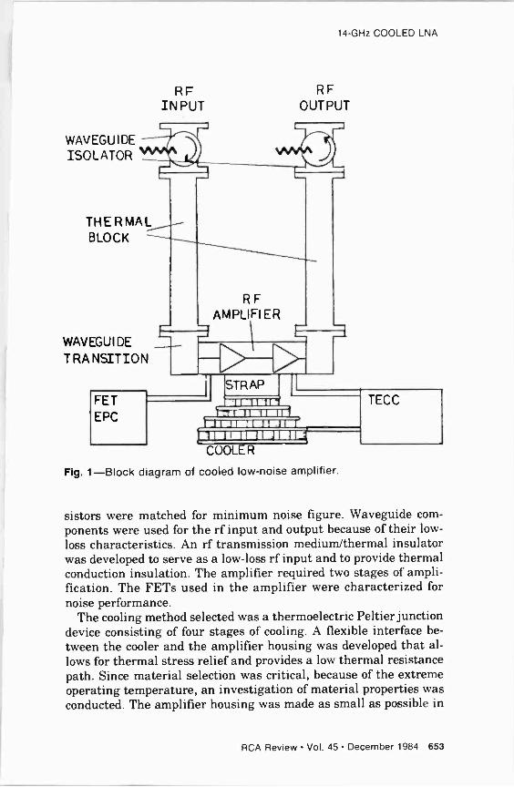
14-GHz COOLED LNA
RF RF IN PUT OUTPUT
WAVEGUIDE ISOLATOR H
THE RMAL BLOCK
WAVEGUI DE
TRANSITION
FE T
EPC
RF AMPLIFIER
COOLER
Fig. 1-Block diagram of cooled low -noise amplifier.
TECC
sistors were matched for minimum noise figure. Waveguide com- ponents were used for the rf input and output because of their low -
loss characteristics. An rf transmission medium/thermal insulator was developed to serve as a low -loss rf input and to provide thermal conduction insulation. The amplifier required two stages of ampli- fication. The FETs used in the amplifier were characterized for noise performance.
The cooling method selected was a thermoelectric Peltier junction device consisting of four stages of cooling. A flexible interface be-
tween the cooler and the amplifier housing was developed that al- lows for thermal stress relief and provides a low thermal resistance path. Since material selection was critical, because of the extreme operating temperature, an investigation of material properties was conducted. The amplifier housing was made as small as possible in
RCA Review Vol. 45 December 1984 653
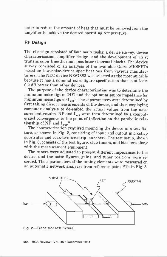
order to reduce the amount of heat that must be removed from the amplifier to achieve the desired operating temperature.
RF Design
The rf design consisted of four main tasks: a device survey, device characterization, amplifier design, and the development of an rf transmission line/thermal insulator (thermal block). The device survey consisted of an analysis of the available GaAs MESFETs based on low -noise -device specifications from various manufac- turers. The NEC device NE67383 was selected as the most suitable because it has a nominal noise -figure specification that is at least 0.2 dB better than other devices.
The purpose of the device characterization was to determine the minimum noise figure (NF) and the optimum source impedance for minimum noise figure (Fops). These parameters were determined by first taking direct measurements of the device, and then employing computer analysis to de -embed the actual values from the mea- surement results. NF and I'opt were then determined by a comput- erized convergence to the point of inflection on the parabolic rela- tionship of NF and I'opt.8
The characterization required mounting the device in a test fix- ture, as shown in Fig. 2, consisting of input and output microstrip substrates and coax-to-microstrip launchers. The test setup, shown in Fig. 3, consists of the test figure, stub tuners, and bias tees along with the measurement equipment.
The tuners were adjusted to present different impedances to the device, and the noise figures, gains, and tuner positions were re- corded. The s parameters of the tuning elements were measured on an automatic network analyzer from reference point PTa in Fig. 3.
SMA
Fig. 2-Transistor test fixture.
SMA
654 RCA Review Vol. 45 December 1984
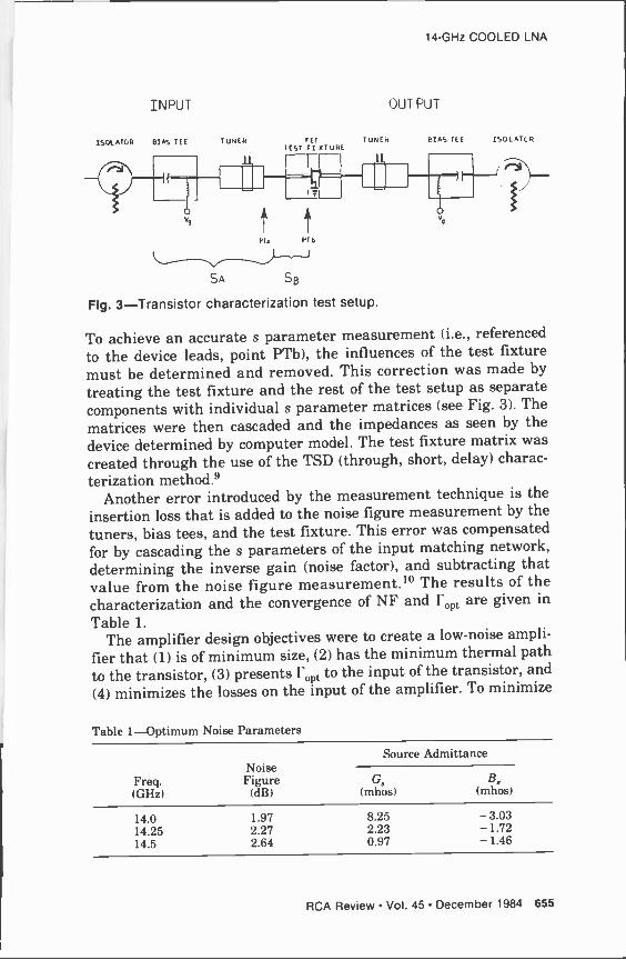
14-GHz COOLED LNA
INPUT
I50LATOR BIAS TEE
v9
TUNER
OU1 PUT
FET TUNES BIAS TEE ISOLATOR EST TI XTURE
t PIA PI b
SA SB
Fig. 3-Transistor characterization test setup.
To achieve an accurate s parameter measurement (i.e., referenced
to the device leads, point PTb), the influences of the test fixture
must be determined and removed. This correction was made by
treating the test fixture and the rest of the test setup as separate components with individual s parameter matrices (see Fig. 3). The
matrices were then cascaded and the impedances as seen by the
device determined by computer model. The test fixture matrix was
created through the use of the TSD (through, short, delay) charac-
terization method.9 Another error introduced by the measurement technique is the
insertion loss that is added to the noise figure measurement by the
tuners, bias tees, and the test fixture. This error was compensated
for by cascading the s parameters of the input matching network,
determining the inverse gain (noise factor), and subtracting that value from the noise figure measurement.10 The results of the characterization and the convergence of NF and ropt are given in
Table 1.
The amplifier design objectives were to create a low -noise ampli-
fier that (1) is of minimum size, (2) has the minimum thermal path
to the transistor, (3) presents F,, to the input of the transistor, and
(4) minimizes the losses on the input of the amplifier. To minimize
Table 1-Optimum Noise Parameters
Source Admittance Noise
Freq. Figure G BA
(GHz) (dB, (mhos) (mhos)
14.0 1.97 8.25 -3.03 14.25 2.27 2.23 -1.72 14.5 2.64 0.97 -1.46
RCA Review Vol. 45 December 1984 655
the thermal path and the size, the transistors and substrates were designed to be mounted directly to the housing, as opposed to using a pallet and mounting the pallet to the housing. This method pre- sents some unique fabrication problems based mainly on size, but allows the total amplifier to be housed in a chassis of dimension 1
x 0.5 x 0.5 inches. The matching circuits were realized using microstrip matching
techniques on a 10 -mil alumina substrate with a chrome, copper, gold metallization scheme. The intent of the matching was to present Vow,, to the input of the device and S22' to the output. Cas- caded impedance transformers were used to create the desired impedance. The circuits were optimized on SuperCompact,i the mi- crowave computer-analysis/optimization software. Bias was at- tained through the use of 1/4 -wavelength shunt elements.
A single -stage amplifier was fabricated and assembled. Its per- formance is shown in Figs. 4 and 5. The matching circuits were adjusted based on the single -stage performance, and a two -stage amplifier was created. The performance of the two -stage amplifier is shown in Figs. 6 and 7. Based upon the temperature performance of the two stage amplifier, the cooling point of -50°C was chosen (see Fig. 8).
The two -stage housing is an H -type construction with the rf cir- cuitry in the top cavity and the dc components in the bottom cavity. Waveguide-to-microstrip transitions (probe type) are used as the transmission medium for the input and output of the amplifier.
To minimize the thermal conduction into the amplifier from the external environment, an rf transmission medium with low inser- tion loss and high thermal resistance was required. The low inser- tion loss is required to avoid increasing the noise figure of the amplifier, since this component will be on the amplifier input. Wave - guide components were used in this application because of their low -loss characteristics. Several different waveguide configurations were tested, and the best results (i.e., lowest insertion loss and highest thermal resistance) were achieved with a waveguide made of plastic and plated on the interior and flange surfaces.' The plating is designed to be thick enough to provide low -loss rf trans- mission, but thin enough to keep the thermal conduction to a min- imum. The plastic used is an ABS polycarbonate (Cycoloy'.). Cycoloy
t Registered trademark of Comsat General Integrated Systems, Inc., Palo Alto, CA 94303. $ Registered trademark of Borg-Warner, Corp., Parkersburg, WV 26101.
656 RCA Review Vol. 45 December 1984
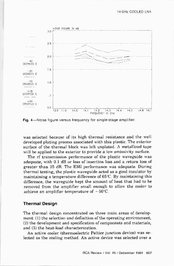
3.0
2.5
NOISE FIGURE IN dB r - -- -
14-GHz COOLED LNA
` /_ 2.0
40 .. _ DEGREES C
1.5 -20 DEGREES C
-10 DEGREES C
1.0
+10 DEGREES C .5
+20 DEGREES C
00 13.6 13.9 14.0 14.1 14.2 14.3 14.4 14.5 14.6 14.7
FREOUENC+ IN GHz
Fig. 4-Noise figure versus frequency for single -stage amplifier.
was selected because of its high thermal resistance and the well developed plating process associated with this plastic. The exterior surface of the thermal block was left unplated. A metallized tape will be applied to the exterior to provide a low emissivity surface.
The rf transmission performance of the plastic waveguide was adequate, with 0.1 dB or less of insertion loss and a return loss of greater than 25 dB. The EMI performance was adequate. During thermal testing, the plastic waveguide acted as a good insulator by maintaining a temperature difference of 65°C. By maintaining this difference, the waveguide kept the amount of heat that had to be removed from the amplifier small enough to allow the cooler to achieve an amplifier temperature of - 50°C.
Thermal Design
The thermal design concentrated on three main areas of develop- ment: (1) the selection and definition of the operating environment, (2) the development and specification of components and materials, and (3) the heat -load characterization.
An active cooler (thermoelectric Peltier junction device) was se- lected as the cooling method. An active device was selected over a
RCA Review Vol. 45 December 1984 657
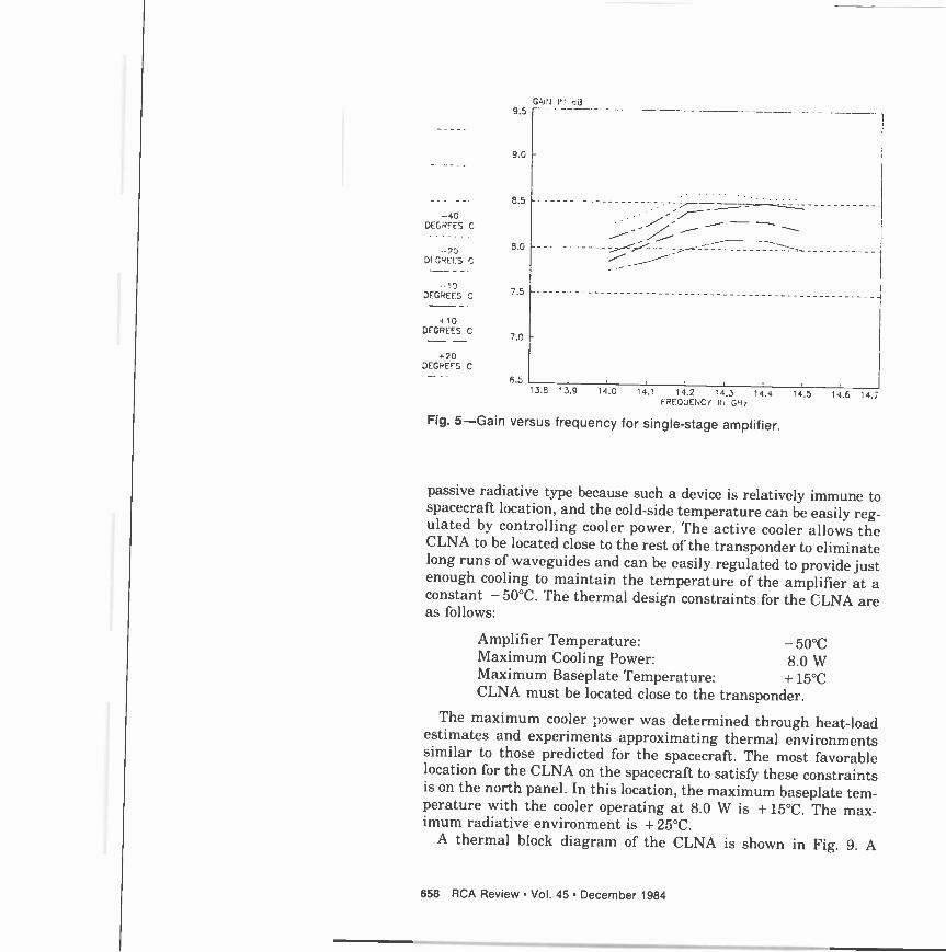
-40 DEGREES C
-- 70 DEGREES C
- 10 DEGREES C
-I10 DEGREES C
+20 DEGREES C
9.0
8.5
9.0
7.5
7.0
6.5
Gaud Ir! c8
13.8 13.9 14.0 14.1 14.2 14.3 14A 14.5 14.6 14.7 FREQUENCY 11i GHz
Fig. 5-Gain versus frequency for single -stage amplifier.
passive radiative type because such a device is relatively immune to spacecraft location, and the cold -side temperature can be easily reg- ulated by controlling cooler power. The active cooler allows the CLNA to be located close to the rest of the transponder to eliminate long runs of waveguides and can be easily regulated to provide just enough cooling to maintain the temperature of the amplifier at a constant -50°C. The thermal design constraints for the CLNA are as follows:
Amplifier Temperature: -50°C Maximum Cooling Power: 8.0 \V Maximum Baseplate Temperature: + 15°C CLNA must be located close to the transponder.
The maximum cooler power was determined through heat -load estimates and experiments approximating thermal environments similar to those predicted for the spacecraft. The most favorable location for the CLNA on the spacecraft to satisfy these constraints is on the north panel. In this location, the maximum baseplate tem- perature with the cooler operating at 8.0 W is + 15°C. The max- imum radiative environment is + 25°C.
A thermal block diagram of the CLNA is shown in Fig. 9. A
658 RCA Review Vol. 45 December 1984
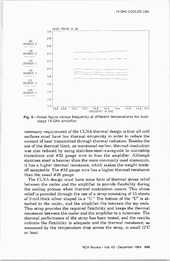
14-GHz COOLED LNA
-60 DEGREES C
-50 DEGREES C
- 40 DEGREES C
- 30 DEGREES C
0.0 DEGREES C
+25 DEGREES C
NOISE FIGURE IN dB 3.0
2.8
2.6
1.4
2.2
2.0
1.8
1.6
7.4
1.2
10 13.8 13.9 14.0 14.1 14.2 14.3 14.4 14.5 14.6 14.7
FREQUENCY IN GHZ
Fig. 6-Noise figure versus frequency at different temperatures for dual - stage 14-GHz amplifier.
necessary requirement of the CLNA thermal design is that all cold surfaces must have low thermal emissivity in order to reduce the amount of heat transmitted through thermal radiation. Besides the use of the thermal block, as mentioned earlier, thermal conduction was also reduced by using stainless-steel-waveguide to microstrip transitions and #32 gauge wire to bias the amplifier. Although stainless steel is heavier than the more commonly used aluminum, it has a higher thermal resistance, which makes the weight trade- off acceptable. The #32 gauge wire has a higher thermal resistance than the usual #26 gauge.
The CLNA design must have some form of thermal stress relief between the cooler and the amplifier to provide flexibility during the cooling process when thermal contraction occurs. This stress relief is provided through the use of a strap consisting of 15 sheets of 2 -mil -thick silver shaped in a "U." The bottom of the "U" is at- tached to the cooler, and the amplifier fits between the top ends. This strap provides the required flexibility and keeps the thermal resistance between the cooler and the amplifier to a minimum. The thermal performance of the strap has been tested, and the results indicate the flexibility is adequate and the thermal resistance, as measured by the temperature drop across the strap, is small (2°C or less).
RCA Review Vol. 45 December 1984 659
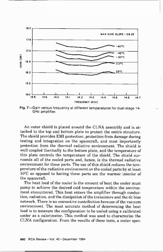
18.0
17.5
17.0
16.5
CD
16.0
15.5
15.0
MAX GAIN SLOPE c 0.6 dB
-60°C
-45°C -30°C
...0.0^°"""^". 0.0°C
25°C
13.8
1 I I I l 1 I I
13.9 14.0 14.1 14.2 14.3 14.4 14.5 14.6
FREQUENCY (GHz)
14.7
Fig. 7-Gain versus frequency at different temperatures for dual -stage 14- GHz amplifier.
An outer shield is placed around the CLNA assembly and is at- tached to the top and bottom plate to protect the entire structure. The shield provides EMI protection, protection from damage during testing and integration on the spacecraft, and most importantly protection from the thermal radiative environment. The shield is well coupled thermally to the bottom plate, and the temperature of this plate controls the temperature of the shield. The shield sur- rounds all of the cooled parts and, hence, is the thermal radiative environment for these parts. The use of this shield 1 -educes the tem- perature of the radiative environment on the cooled parts by at least 10°C as opposed to having these parts see the warmer interior of the spacecraft.
The heat load of the cooler is the amount of heat the cooler must pump to achieve the desired cold temperature within the environ- ment encountered. This heat enters the amplifier through conduc- tion, radiation, and the dissipation of the transistors and the dc bias network. There is no convective contribution because of the vacuum environment. The most accurate method of determining the heat load is to measure the configuration to be cooled using a calibrated cooler as a calorimeter. This method was used to characterize the CLNA configuration. From the results of these tests, a cooler spec -
660 RCA Review Vol. 45 December 1984
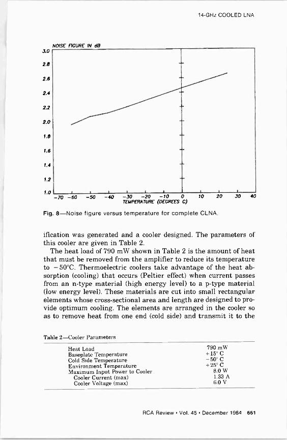
14-GHz COOLED LNA
3.0
2.8
2.6
2.4
2.2
2.0
1.8
1.6
1.4
1.2
10
NOISE FIGURE IN dB
-70 -60 -50 -40 -30 -20 -10 0 10 TEMPERATURE (DEGREES C)
' 20 30
Fig. 8-Noise figure versus temperature for complete CLNA.
40
ification was generated and a cooler designed. The parameters of this cooler are given in Table 2.
The heat load of 790 mW shown in Table 2 is the amount of heat that must be removed from the amplifier to reduce its temperature to - 50°C. Thermoelectric coolers take advantage of the heat ab- sorption (cooling) that occurs (Peltier effect) when current passes from an n -type material (high energy level) to a p -type material (low energy level). These materials are cut into small rectangular elements whose cross-sectional area and length are designed to pro- vide optimum cooling. The elements are arranged in the cooler so as to remove heat from one end (cold side) and transmit it to the
Table 2-Cooler Parameters
Heat Load 790 mW Baseplate Temperature + 15° C
Cold Side Temperature -50° C
Environment Temperature + 25° C
Maximum Input Power to Cooler 8.0 W Cooler Current (max) 1.33 A
Cooler Voltage (max) 6.0 V
RCA Review Vol. 45 December 1984 661
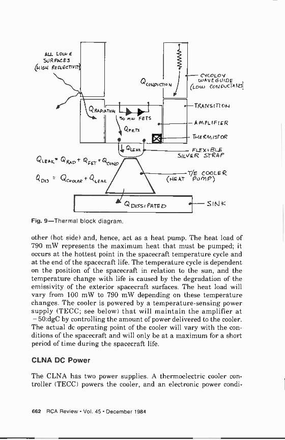
ALL Low E
SURFACE S
& IGN REcirCTIv
+CIEAk- QRAPt 4FET * -Co
QolS yCo(x.tR `t.EAK
Fig. 9-Thermal block diagram.
QCOWpvQlo N I) CYcoLoY
wAvEGUiDE (Low CONDUCTAkt1
TRANsITIoN
AMPLIFIER
TNEMfsroR
FLEX BLF SILVER sr -RAP
Y/E COOLER (NEAT PUMP)
SIN
other (hot side) and, hence, act as a heat pump. The heat load of 790 mW represents the maximum heat that must be pumped; it occurs at the hottest point in the spacecraft temperature cycle and at the end of the spacecraft life. The temperature cycle is dependent on the position of the spacecraft in relation to the sun, and the temperature change with life is caused by the degradation of the emissivity of the exterior spacecraft surfaces. The heat load will vary from 100 mW to 790 mW depending on these temperature changes. The cooler is powered by a temperature -sensing power supply (TECC; see below) that will maintain the amplifier at - 50:dgC by controlling the amount of power delivered to the cooler. The actual dc operating point of the cooler will vary with the con- ditions of the spacecraft and will only be at a maximum for a short period of time during the spacecraft life.
CLNA DC Power
The CLNA has two power supplies. A thermoelectric cooler con- troller (TECC) powers the cooler, and an electronic power condi-
662 RCA Review Vol. 45 December 1984
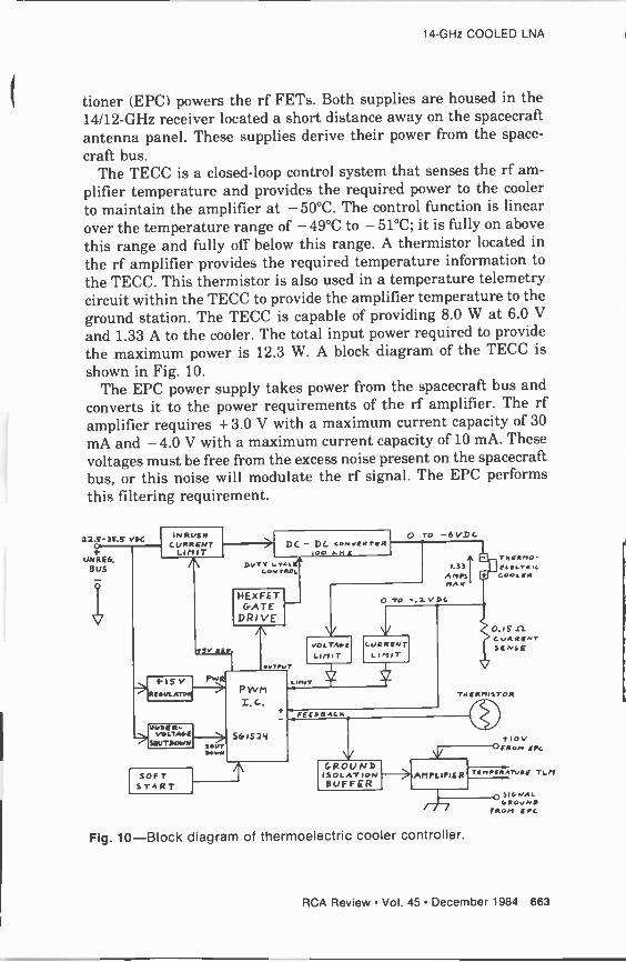
14-GHz COOLED LNA
tioner (EPC) powers the rf FETs. Both supplies are housed in the 14/12-GHz receiver located a short distance away on the spacecraft antenna panel. These supplies derive their power from the space-
craft bus. The TECC is a closed -loop control system that senses the rf am-
plifier temperature and provides the required power to the cooler
to maintain the amplifier at -50°C. The control function is linear over the temperature range of - 49°C to - 51°C; it is fully on above
this range and fully off below this range. A thermistor located in
the rf amplifier provides the required temperature information to
the TECC. This thermistor is also used in a temperature telemetry circuit within the TECC to provide the amplifier temperature to the ground station. The TECC is capable of providing 8.0 W at 6.0 V
and 1.33 A to the cooler. The total input power required to provide
the maximum power is 12.3 W. A block diagram of the TECC is
shown in Fig. 10. The EPC power supply takes power from the spacecraft bus and
converts it to the power requirements of the rf amplifier. The rf amplifier requires +3.0 V with a maximum current capacity of 30
mA and -4.0 V with a maximum current capacity of 10 mA. These voltages must be free from the excess noise present on the spacecraft bus, or this noise will modulate the rf signal. The EPC performs this filtering requirement.
22.E-35.5 vac
UNRE6. Bus
Q
V
-
INRUSH CURRENT
LIMIT
+15 V
REbVLAToR
-----T DC. - DC cor.rveRreR 1°o wM1
DUTY cYLLEa cow rROL
HEXFET GATE
DRIVE
oVrPT
PwR
uNDE R - VOLTA[
SMVTDOwW
SOFT START
SYv{ lo rR
PwM I. G.
S61S2y
p ro -6VDC
vO LTAct LIMIT
LIMIT
r1,161¢110- 1.33 ELEtru,
1.1Pí Goo LER MA ><
O TO -.2 V AC
CURRENT LIMIT
FEED9ACR
0.15 n CVRIIEtiT SENSE
TN ER MIS TOR
V GROUND
ISOLATION BUFFER
>1ArIPLIFiER
t1GV OFROM EPC
TenPERATURE TLM
Fig. 10-Block diagram of thermoelectric cooler controller.
O 516, ,AL L 4ROV,D
FROM EPC
RCA Review Vol. 45 December 1984 663
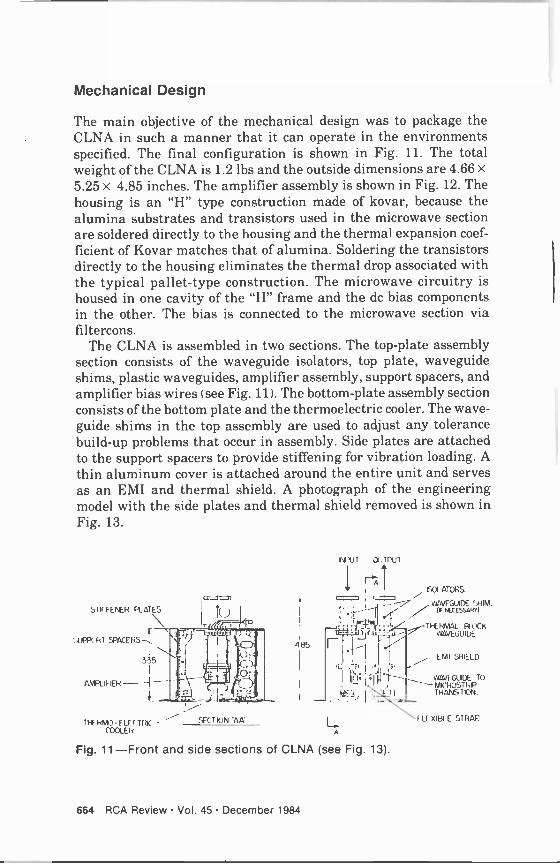
Mechanical Design
The main objective of the mechanical design was to package the CLNA in such a manner that it can operate in the environments specified. The final configuration is shown in Fig. 11. The total weight of the CLNA is 1.2 lbs and the outside dimensions are 4.66 x
5.25 x 4.85 inches. The amplifier assembly is shown ín Fíg. 12. The housing is an "H" type construction made of kovar, because the alumina substrates and transistors used in the microwave section are soldered directly to the housing and the thermal expansion coef- ficient of Kovar matches that of alumina. Soldering the transistors directly to the housing eliminates the thermal drop associated with the typical pallet -type construction. The microwave circuitry is housed in one cavity of the "H" frame and the dc bias components in the other. The bias is connected to the microwave section via filtercons.
The CLNA is assembled in two sections. The top -plate assembly section consists of the waveguide isolators, top plate, waveguide shims, plastic waveguides, amplifier assembly, support spacers, and amplifier bias wires (see Fig. 11). The bottom -plate assembly section consists of the bottom plate and the thermoelectric cooler. The wave - guide shims in the top assembly are used to adjust any tolerance build-up problems that occur in assembly. Side plates are attached to the support spacers to provide stiffening for vibration loading. A
thin aluminum cover is attached around the entire unit and serves as an EMI and thermal shield. A photograph of the engineering model with the side plates and thermal shield removed is shown in Fig. 13.
THFHMO-ELECTRIC - COOLEk.
SECTION 'AA
485
INPUT OUTPUT
1 I ISOLATORS.
1
11.11 11.1
I i=-1 I
Fig. 11-Front and side sections of CLNA (see Fig. 13).
WAVEGUIDE SHIM. (f hECE55aRY1
THERMAL EtCCK WAVEGUIDE.
EMI SHIELD
WAVFGUIDE TO - - MICROSTRIP
I RANSITION.
FLEXIBLE STRAP.
664 RCA Review Vol. 45 December 1984
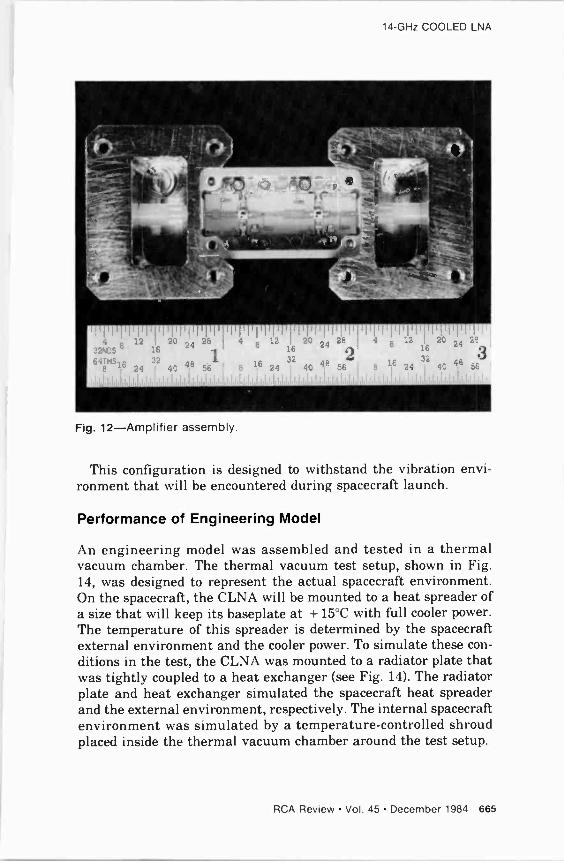
14-GHz COOLED LNA
n
rc)-.y r 1
Il / t.!
III'III'1'I'I1IIII1II1l1lT1Tl1I'II1TI11'ITI'I1'1'I11'l'1'Il'I'I'III'11111T11'I111I1III 11111
4 8 12 20 24 28 4 8 12 20 24
28 4 8
12 20 24 28
32N05 16 16 16 3
69TM516 32 4B 16 32 48 16 32 48
8 24 l 40 56 B 24 1 90 56 B I 24 I 40 56
1,L I I614111,161,Id l,I Id IJ I 1Jlil d ld i,6LJ 1, I i, L I'dm ,i, ,I 1, I,
Fig. 12-Amplifier assembly.
This configuration is designed to withstand the vibration envi- ronment that will be encountered during spacecraft launch.
Performance of Engineering Model
An engineering model was assembled and tested in a thermal vacuum chamber. The thermal vacuum test setup, shown in Fig. 14, was designed to represent the actual spacecraft environment. On the spacecraft, the CLNA will be mounted to a heat spreader of a size that will keep its baseplate at + 15°C with full cooler power. The temperature of this spreader is determined by the spacecraft external environment and the cooler power. To simulate these con- ditions in the test, the CLNA was mounted to a radiator plate that was tightly coupled to a heat exchanger (see Fig. 14). The radiator plate and heat exchanger simulated the spacecraft heat spreader and the external environment, respectively. The internal spacecraft environment was simulated by a temperature -controlled shroud placed inside the thermal vacuum chamber around the test setup.
RCA Review Vol. 45 December 1984 665
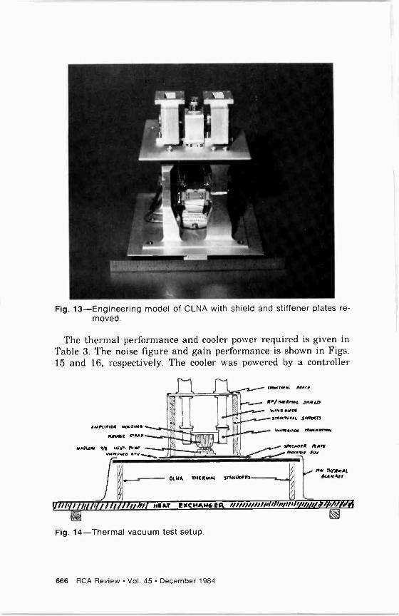
Fig. 13-Engineering model of CLNA with shield and stiffener plates re- moved.
The thermal performance and cooler power required is given in Table 3. The noise figure and gain performance is shown in Figs. 15 and 16, respectively. The cooler was powered by a controller
MellllfR MOUI'NO
MARLOM T/! Mfi. Pure uMn..eo ATVr`
UNA TNERPMI SrRNOOiFS"
4
IleuIae1M
R//RdRmel JM/P/0 wave eJof RIIULNleL SMMr7
welwor IRMe.fiilreN
1///fi¡///1/1//W//¡/l//% HAT lXCHANili¿
Fig. 14-Thermal vacuum test setup.
sPrrwoeR RR/F elr.erthf HN
Pew A/FMIRI ~NAZI
/i///iiiiimIi/Ytfi/PIPp/i/i/PWW,f1
666 RCA Review Vol. 45 December 1984
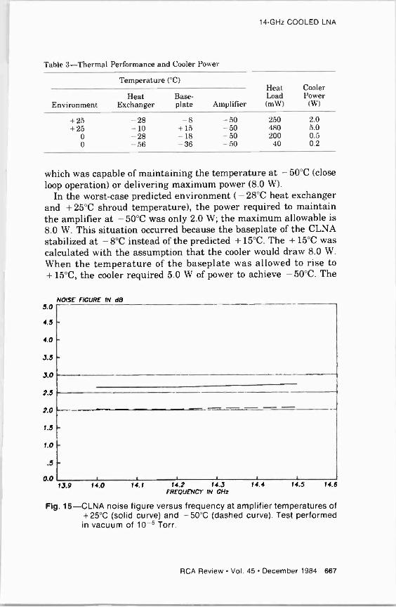
14-GHz COOLED LNA
Table 3-Thermal Performance and Cooler Power
Temperature (°C) Heat Cooler
Heat Base- Load Power Environment Exchanger plate Amplifier (mW) (W)
+25 -28 -8 -50 250 2.0 +25 -10 +15 -50 480 5.0
0 -28 -18 -50 200 0.5 0 -56 -36 -50 40 0.2
which was capable of maintaining the temperature at - 50°C (close loop operation) or delivering maximum power (8.0 W).
In the worst -case predicted environment (- 28°C heat exchanger and + 25°C shroud temperature), the power required to maintain the amplifier at -50°C was only 2.0 W; the maximum allowable is 8.0 W. This situation occurred because the baseplate of the CLNA stabilized at - 8°C instead of the predicted + 15°C. The + 15°C was calculated with the assumption that the cooler would draw 8.0 W.
When the temperature of the baseplate was allowed to rise to +15°C, the cooler required 5.0 W of power to achieve -50°C. The
5.0
4.5
4.0
3.5
3.0
2.5
2.0
1.5
1.0
.5
0.0
NOISE FIGURE IN dB
13.9 I
l 14.0 14.1 14.2 14.3
FREQUENCY IN GHz I 14.4 14.5 14.6
Fig. 15-CLNA noise figure versus frequency at amplifier temperatures of +25°C (solid curve) and -50°C (dashed curve). Test performed in vacuum of 10-5 Torr.
RCA Review Vol. 45 December 1984 667
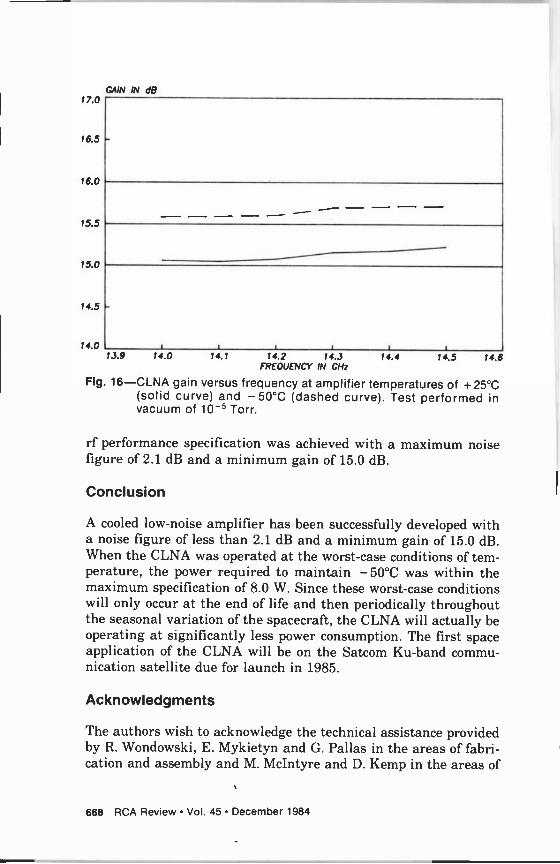
17.0
16.5
16.0
15.5
15.0
GAIN IN de
14.5 I-
14.0 13.9 14.2 14.3
FREQUENCY IN GHz
Fig. 16-CLNA gain versus frequency at amplifier temperatures of +25°C (solid curve) and -50°C (dashed curve). Test performed in vacuum of 10-5 Torr.
14.0 14.1 14.4 14.5 14.6
rf performance specification was achieved with a maximum noise figure of 2.1 dB and a minimum gain of 15.0 dB.
Conclusion
A cooled low -noise amplifier has been successfully developed with a noise figure of less than 2.1 dB and a minimum gain of 15.0 dB. When the CLNA was operated at the worst -case conditions of tem- perature, the power required to maintain - 50°C was within the maximum specification of 8.0 W. Since these worst -case conditions will only occur at the end of life and then periodically throughout the seasonal variation of the spacecraft, the CLNA will actually be operating at significantly less power consumption. The first space application of the CLNA will be on the Satcom Ku -band commu- nication satellite due for launch in 1985.
Acknowledgments
The authors wish to acknowledge the technical assistance provided by R. Wondowski, E. Mykietyn and G. Pallas in the areas of fabri- cation and assembly and M. McIntyre and D. Kemp in the areas of
668 RCA Review Vol. 45 December 1984
14-GHz COOLED LNA
electrical and rf testing. The guidance and insight of H. Zelen, R. McCann, E. Morse, P. Wise and H. Strickberger provided invalu- able ín the completion of this task and deserve special thanks.
References:
1 J. Napoli, "GSTAR-A High Performance Ku -Band Satellite for the 1980s" AIAA 9th Communications Satellite Cont., pp. 436-447, March 1982.
2 M. Nogami, Y. Hirach, and K. Ohta, "Present State of Microwave GaAs Devices," Microelectronics J., 13, No. 3, p. 29 (1983).
3 C. A. Liechti and R. B. Larrick, "Performance of GaAs MESFETS at Low Tem- peratures," IEEE Trans. Microwave Theory and Tech., MTT-24, p. 376, June 1976.
4 H. L. Hung and N. L Hyman, "Thermoelectrically Cooled MESFET Low -Noise Am- plifier for Earth Stations," Comstat Tech. Review, 10, No. 2, p. 299, Fall 1980.
Sander Weinreb, "Low -Noise Cooled GaAs FET Amplifiers," IEEE Trans. Micro- wave Theory and Tech., MTT-28, No. 10, p. 1041, Oct. 1980.
6 A. Cappello and J. Pierro, "A 22 to 24 GHz Cryogenically Cooled Low -Noise FET
Amplifier in Co -planar Waveguide," IEEE MTT-s Digest 1982, pp. 19-22. 7 J. Pierro, "Cryogenically Cooled GaAs FET Amplifier with a Noise Temperature
Under 70 K at 5.0 GHz," IEEE Trans. Microwave Theory and Tech., p. 972, Dec. 1976.
6 R. Lane, "The Determination of Device Noise Parameters," Proc. IEEE (letters), 57, p. 1461, Aug. 1969.
9 N. R. Frazen and R. A. Speciale, "A New Procedure for System Calibration and Error Removal in Automated S -Parameter Measurements," Proc. 5th European Mi- crowave Conf. (Hamburg, Germany), Sept. 1-4, pp. 69-73 (1975). t0 E. W. Strid, "Noise Measurement Checklist Eliminates Costly Errors," Microwave System News., p. 88, Dec. 1981.
RCA Review Vol. 45 December 1984 669
20-GHz Lumped -Element GaAs FET Driver Amplifier
S. S. Moochalla and D. E. Aubert RCA Astro -Electronics, Princeton, NJ 08540
Abstract-A wideband lumped -element 20-GHz driver amplifier using GaAs FET chip devices for a 30/20-GHz communications sat- ellite is described. Also described is a wideband 17- to 22-GHz low -loss waveguide-to-microstrip transition developed to pro- vide the input and output connections to the microstrip am- plifiers. An rf output power level of 17 dBm and 12 -dB gain over the 17.7- to 20.2-GHz band was achieved using two stages.
1. Introduction
Increasing use is being made of the 30/20-GHz frequency range for satellite communications. Downlink, 20-GIIz travelling -wave -tube amplifiers (TWTAs) require linear driver amplifiers for added gain capability. The 20-GHz driver amplifier described here uses lumped -element matched GaAs FET chip devices and provides an output level greater than 13 dBm to drive the TWTAs.
At 20 GHz, a waveguide is the most common transmission me- dium due to its low loss characteristics. The most convenient media for impedance matching GaAs FET amplifiers, however, are 50 -ohm microstrip input and output sections. Therefore, a waveguide-to- microstrip transition was developed. Lumped -element matching networks (bond wires, ribbons and capacitors) are used, since they incorporate the parasitic elements in the device -to -circuit interface, thus allowing maximum attainable power and gain by the device.' Smaller circuit sizes (less weight) and wider bandwidths are also possible with lumped -element matching.2
Single -stage lumped -element matched amplifiers mounted on gold plated copper carriers were developed individually. The input
670 RCA Review Vol. 45 December 1984
20-GHz FET AMPLIFIER
amplifier, which uses an AT -8041 FET, was cascaded with the output amplifier, which uses a DLX-3504A FET.".
The waveguide-to-microstrip transition is discussed first. The in-
dividual stages of the amplifier are then discussed, together with the chip carrier design. Finally test results for the full amplifier are presented.
2. Waveguide-to-Microstrip Transition
The 20-GHz transition was designed for a WR-42 rectangular wave - guide and a microstrip using a 15 -mil quartz substrate.3.1° The de-
sign of such a transition is essentially that of an impedance trans- former. There are, however, four different definitions of impedance for rectangular waveguides: voltage -current, power -voltage, power - current, and E -H. For the impedance -matching applications, studies by Chen4 and Mihran5 have shown that for ridge waveguides the V -I definition is the most convenient. A four -step Chebyshev quar- terwave transformer method was used to transform the waveguide impedance to the 50 ohms of the microstrip. The ridge width is kept constant and the gap is varied to obtain the desired impedances of the transformer. Corrections in the length of the quarterwave trans- formers were calculated using rectangular waveguide approxima- tions. The ridge waveguide was considered to be equivalent to a
rectangular waveguide, with the guide wavelength given by the ridge-waveguide parameters.
Higher order modes are generated at the wageguide-microstrip junction. To prevent these higher order modes from being trans- mitted, resulting in losses, a small rectangular cover with cutoff waveguide dimensions is placed at this junction (Fig. 1). The di-
mensions of this cover were calculated using the approximate for-
mula, given by Schneider,'
]i (E, - 1)]
b E,.
where ff. is the first higher -order -mode cutoff frequency, a the cover width, b the cover height, h the substrate thickness, and E,. is the relative dielectric constant. According to this equation, when a =
0.24 inch and b = 0.17 inch, then fc = 23.8 GHz, which is above the upper band edge (20.2 GHz). Fig. 1 shows the two waveguide-
t Avantek Inc., Santa Clara, CA 95051. Dexcel Div., Gould Inc., Santa Clara, CA 95050.
RCA Review Vol. 45 December 1984 671
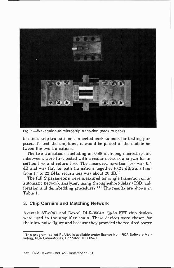
..r
Fig. 1-Waveguide-to-microstrip transition (back to back).
to-microstrip transitions connected back-to-back for testing pur- poses. To test the amplifier, it would be placed in the middle be- tween the two transitions.
The two transitions, including an 0.88 -inch -long microstrip line inbetween, were first tested with a scalar network analyzer for in- sertion loss and return loss. The measured insertion loss was 0.5 dB and was flat for both transitions together (0.25 dB/transition) from 17 to 22 GHz; return loss was about 20 dB.1°
The full S parameters were measured for single transition on an automatic network analyzer, using through -short -delay (TSD) cal- ibration and deimbedding procedures.`11 The results are shown in Table 1.
3. Chip Carriers and Matching Network
Avantek AT -8041 and Dexcel DLX-3504A GaAs FET chip devices were used in the amplifier chain. These devices were chosen for their low noise figure and because they provided the required power
This program, called PLANA, is available under license from RCA Software Mar- keting, RCA Laboratories, Princeton, NJ 08540.
672 RCA Review Vol. 45 December 1984
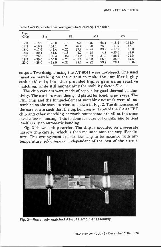
20-GHz FET AMPLIFIER
Table l -S Parameters for Waveguide-to-Microstrip Transition
Freq. (GHz) Sil S21 SI2 S22
17.0 -18.2 -175.8 -.15 -66.4 -.15 -66.4 -18.9 -134.0 17.5 -16.9 161.1 - .20 76.2 - .20 76.2 -17.0 168.1 18.0 -17.6 149.4 -.25 39.9 -.25 39.9 -17.7 105.8 18.5 -20.4 141.6 -.18 4.2 -.18 4.2 -20.6 48.8 19.0 -26.2 139.4 -.22 -31.9 -.22 -31.9 -26.9 -21.5 19.5 -39.0 -55.0 - .23 -66.5 - .23 -66.5 -36.6 167.5 20.0 -28.0 -38.9 -.22 79.7 -.22 79.7 -29.1 8.07
output. Two designs using the AT -8041 were developed. One used resistive matching on the output to make the amplifier highly stable (K > 1); the other provided higher gain using reactive matching, while still maintaining the stability factor K > 1.
The chip carriers were made of copper for good thermal conduc- tivity. The carriers were then gold plated for bonding purposes. The FET chip and the lumped -element matching network were all as- sembled on the same carrier, as shown in Fig. 2. The dimensions of the carrier are such that,the top bonding surfaces of the GAAs FET chip and other matching network components are all at the same level after mounting. This is done for ease of bonding and to lend itself easily to automatic bonding.
Fig. 3 shows a chip carrier. The chip is mounted on a separate narrow chip carrier, which is then mounted onto the amplifier fix- ture. This arrangement enables the chip to be mounted with any temperature solder/epoxy, independent of the rest of the circuit.
r , iIL
o
--- rt
Fig. 2 -Resistively matched AT -8041 amplifier assembly.
= r
RCA Review Vol. 45 December 1984 673
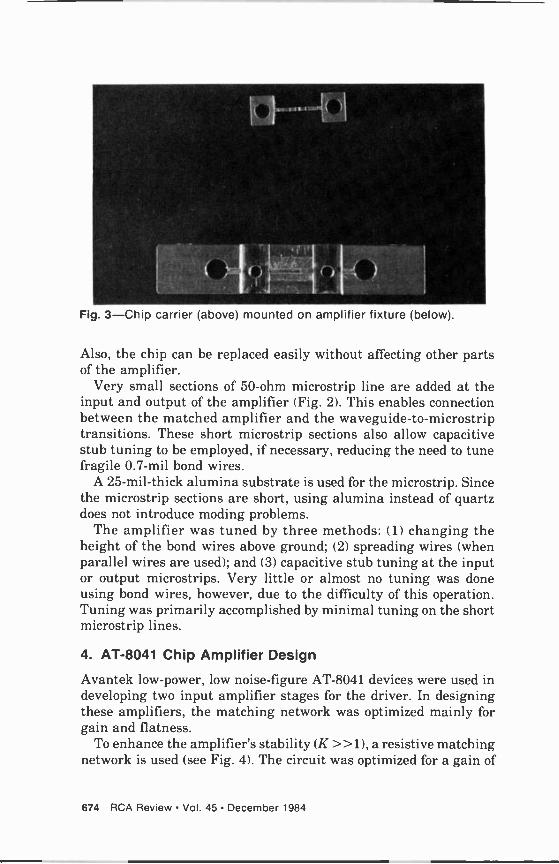
+Al
r t--.
-{ Vi :ri J
t
.
Fig. 3-Chip carrier (above) mounted on amplifier fixture (below).
Also, the chip can be replaced easily without affecting other parts of the amplifier.
Very small sections of 50 -ohm microstrip line are added at the input and output of the amplifier (Fig. 2). This enables connection between the matched amplifier and the waveguide-to-microstrip transitions. These short microstrip sections also allow capacitive stub tuning to be employed, if necessary, reducing the need to tune fragile 0.7 -mil bond wires.
A 25 -mil -thick alumina substrate is used for the microstrip. Since the microstrip sections are short, using alumina instead of quartz does not introduce moding problems.
The amplifier was tuned by three methods: (1) changing the height of the bond wires above ground; (2) spreading wires (when parallel wires are used); and (3) capacitive stub tuning at the input or output microstrips. Very little or almost no tuning was done using bond wires, however, due to the difficulty of this operation. Tuning was primarily accomplished by minimal tuning on the short microstrip lines.
4. AT -8041 Chip Amplifier Design
Avantek low -power, low noise -figure AT -8041 devices were used in developing two input amplifier stages for the driver. In designing these amplifiers, the matching network was optimized mainly for gain and flatness.
To enhance the amplifier's stability (K » 1), a resistive matching network is used (see Fig. 4). The circuit was optimized for a gain of
674 RCA Review Vol. 45 December 1984
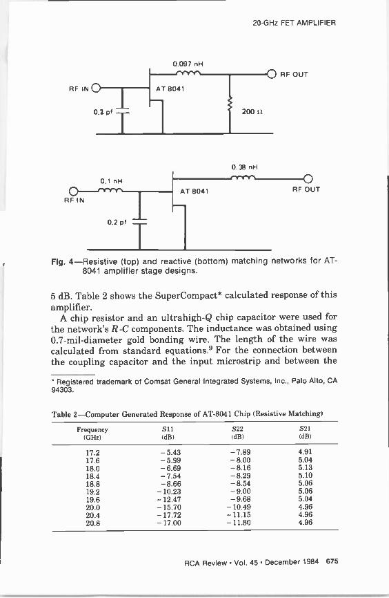
20-GHz FET AMPLIFIER
RF IN
0.1 nH a1t11 RF IN
0.2 p1 --
0.097 nH
RF OUT
0.38 nH
AT 8041 RF OUT
Fig. 4 -Resistive (top) and reactive (bottom) matching networks for AT - 8041 amplifier stage designs.
5 dB. Table 2 shows the SuperCompact* calculated response of this amplifier.
A chip resistor and an ultrahigh -Q chip capacitor were used for the network's R -C components. The inductance was obtained using 0.7 -mil -diameter gold bonding wire. The length of the wire was calculated from standard equations.9 For the connection between the coupling capacitor and the input microstrip and between the
Registered trademark of Comsat General Integrated Systems, Inc., Palo Alto, CA 94303.
Table 2 -Computer Generated Response of AT -8041 Chip (Resistive Matching)
Frequency (GHz)
Sll (dB)
S22 (dB)
S21 (dB)
17.2 -5.43 -7.89 4.91 17.6 -5.99 -8.00 5.04 18.0 -6.69 -8.16 5.13 18.4 -7.54 -8.29 5.10 18.8 -8.66 -8.54 5.06 19.2 -10.23 -9.00 5.06 19.6 -12.47 -9.68 5.04 20.0 -15.70 -10.49 4.96 20.4 -17.72 -11.15 4.96 20.8 -17.00 -11.80 4.96
RCA Review Vol. 45 December 1984 675
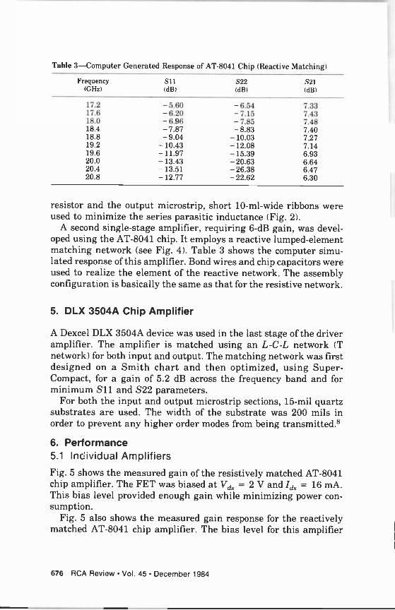
Table 3 -Computer Generated Response of AT -8041 Chip (Reactive Matching)
Frequency (GHz)
Sll (dB)
S22 (dB)
S21 (dB)
17.2 -5.60 -6.54 7.33 17.6 - 6.20 -7.15 7.43 18.0 -6.96 -7.85 7.48 18.4 -7.87 -8.83 7.40 18.8 -9.04 -10.03 7.27 19.2 -10.43 -12.08 7.14 19.6 -11.97 -15.39 6.93 20.0 -13.43 -20.63 6.64 20.4 -13.51 -26.38 6.47 20.8 -12.77 -22.62 6.30
resistor and the output microstrip, short 10 -ml -wide ribbons were used to minimize the series parasitic inductance (Fig. 2).
A second single -stage amplifier, requiring 6 -dB gain, was devel- oped using the AT -8041 chip. It employs a reactive lumped -element matching network (see Fig. 4). Table 3 shows the computer simu- lated response of this amplifier. Bond wires and chip capacitors were used to realize the element of the reactive network. The assembly configuration is basically the same as that for the resistive network.
5. DLX 3504A Chip Amplifier
A Dexcel DLX 3504A device was used in the last stage of the driver amplifier. The amplifier is matched using an L -C -L network (T network) for both input and output. The matching network was first designed on a Smith chart and then optimized, using Super - Compact, for a gain of 5.2 dB across the frequency band and for minimum S11 and S22 parameters.
For both the input and output microstrip sections, 15 -mil quartz substrates are used. The width of the substrate was 200 mils in order to prevent any higher order modes from being transmitted.8
6. Performance 5.1 Individual Amplifiers
Fig. 5 shows the measured gain of the resistively matched AT -8041 chip amplifier. The FET was biased at Vds = 2 V and Ids = 16 mA. This bias level provided enough gain while minimizing power con- sumption.
Fig. 5 also shows the measured gain response for the reactively matched AT -8041 chip amplifier. The bias level for this amplifier
676 RCA Review Vol. 45 December 1984
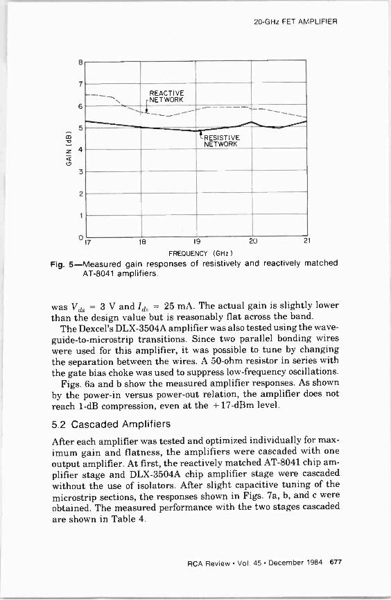
v 2
8
7
6
5
4
3
2
1
017
20-GHz FET AMPLIFIER
REACTIVE NETWORK
RESISTIVE NETWORK
18 19 20 21
FREQUENCY (GHz)
Fig. 5-Measured gain responses of resistively and reactively matched AT -8041 amplifiers.
was Vds = 3 V and Ids = 25 mA. The actual gain is slightly lower than the design value but is reasonably flat across the band.
The Dexcel's DLX-3504A amplifier was also tested using the wave- guide-to-microstrip transitions. Since two parallel bonding wires were used for this amplifier, it was possible to tune by changing the separation between the wires. A 50 -ohm resistor in series with the gate bias choke was used to suppress low -frequency oscillations.
Figs. 6a and b show the measured amplifier responses. As shown by the power -in versus power -out relation, the amplifier does not reach 1 -dB compression, even at the + 17-dBm level.
5.2 Cascaded Amplifiers
After each amplifier was tested and optimized individually for max- imum gain and flatness, the amplifiers were cascaded with one output amplifier. At first, the reactively matched AT -8041 chip am- plifier stage and DLX-3504A chip amplifier stage were cascaded without the use of isolators. After slight capacitive tuning of the microstrip sections, the responses shown in Figs. 7a, b, and c were obtained. The measured performance with the two stages cascaded are shown in Table 4.
RCA Review Vol. 45 December 1984 677
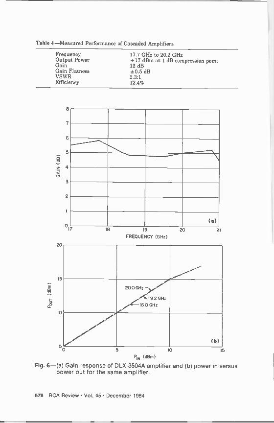
Table 4-Measured Performance of Cascaded Amplifiers
Frequency Output Power Gain Gain Flatness VSWR Efficiency
17.7 GHz to 20.2 GHz + 17 dBm at 1 dB compression point 12dB -±-0.5 dB 2.3:1 12.4%
8
7
6
5 m
z 4
20
15
10
3
2
017
(a) 18 19
FREQUENCY (GHz)
20 21
50 5
20.0 GHz
19.2 GHz
18.0 GHz
10
(b)
15
PIN (dBm )
Fig. 6-(a) Gain response of DLX-3504A amplifier and (b) power in versus power out for the same amplifier.
678 RCA Review Vol. 45 December 1984
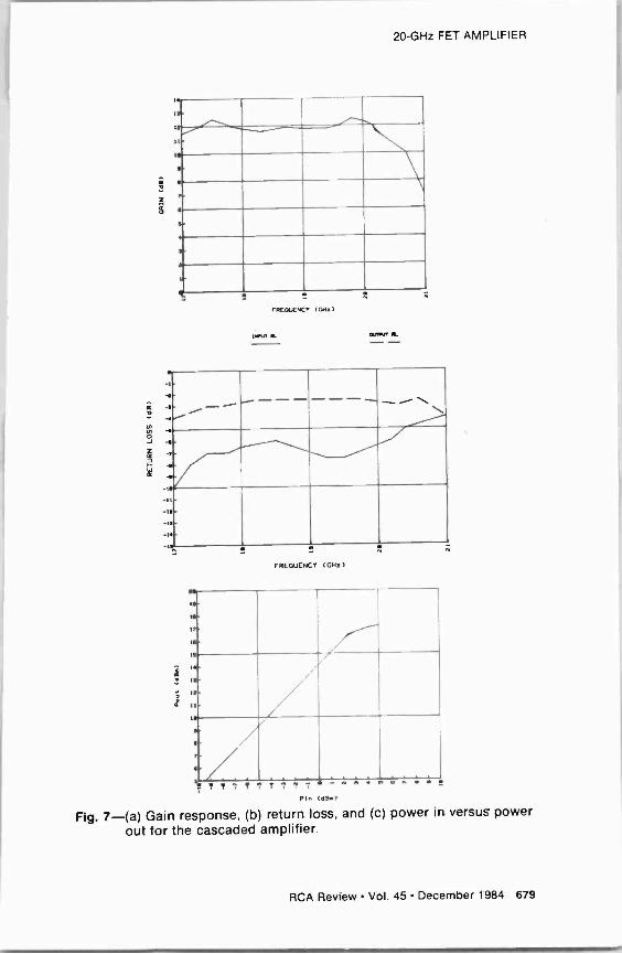
20-GHz FET AMPLIFIER
z
5
FREQUENCY (GHx)
<Unit", R
4'
FREQUENCY (GHz)
I I IT IV
1}
1.
IT
1,-
11.
1
h f / . . . . . . . .
i. e* q T w f A, -
Pin (GBp)
Fig. 7-(a) Gain response, (b) return loss, and (c) power in versus power out for the cascaded amplifier.
RCA Review Vol. 45 December 1984 679
7. Conclusion
The use of lumped -element matching networks and short microstrip lines for tuning has been demonstrated for a 20-GHz driver ampli- fier. This facilitated ease of tuning (and of manufacturability) by not requiring adjustment of fragile bond wires. The small circuits led to small size and low weight, a premium in space applications. Using this approach, a driver amplifier with an output power of + 17 dBm at 1 -dB compression has been developed.
References:
1 K. Honjo, Y. Takayara, and A. Higashiaka, "Broadband Internal Matching of Mi- crowave Power GaAs MESFET's," IEEE Trans. Microwave Theory and Tech., MTT- 24, p 3, Jan. 1979. 2 R. L. Camisa, J. B. Klatskin, D. Haggis, "Fabrication of Lumped -Element Broad- band GaAs MESFET Microwave Power Amplifiers," RCA Review, 42 (4), p 576, Dec. 1981. 3 E. A. Schneider, "Microwave and Millimeter Wave Hybrid Integrated Circuits for Radio Systems," Bell System Tech J., 48, p 1703, July-August 1969. ° S. B. Cohen, "Optimum Design of Stepped Transmission Line Transformers,"
IEEE Trans. Microwave Theory and Tech., p 16, April 1955. T. S. Chen, "Calculation of the Parameters of Ridge Waveguides," IEEE Trans.
Microwave Theory and Tech., p 12, Jan. 1957. 6 T. G. Mihran, "Closed and Open -Ridge Waveguides," IEEE Trans. Microwave Theory and Tech., p 640, June 1949. 7 Matthaei, Young, and Jones, Microwave Filters, Impedance Matching Networks, and Coupling Structures, pp 300-304, Artech House Inc. 8 M. V. Schneider, "Millimeter Wave Integrated Circuits," Bell Laboratories, Craw- ford Hill Laboratories, Holmdel, NJ 01733 9 F. E. Terman, Radio Engineers' Handbook, pp 48-51, McGraw Hill Book Co., Inc. (1943). ° S. S. Moochala and C. An, "Ridge Waveguide Used in Microstrip Transition," Microwaves and RF, 23 (3), p 149, March 1984. "J. L. Schepps and D. L. Rhodes, "PLANA/2.0 New Control Software for the Hew- lett Packard 8409 Network Analyzer System," ARFTG 21st Workshop Digest, Bur- lington, MA, June 1983.
680 RCA Review Vol. 45 December 1984
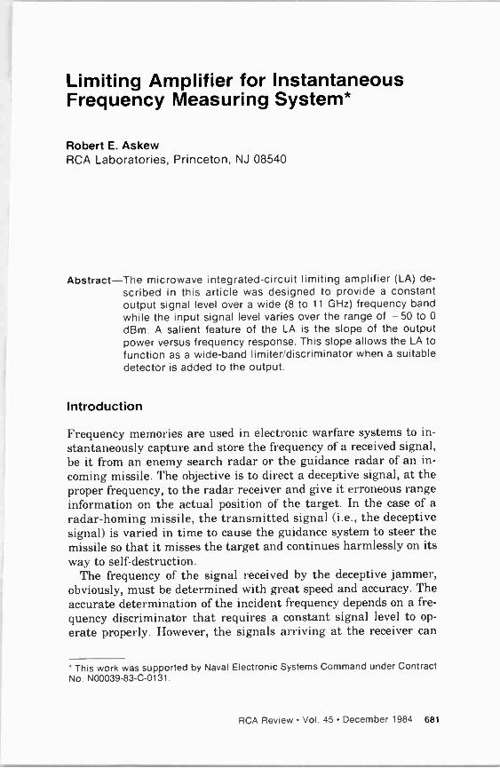
Limiting Amplifier for Instantaneous Frequency Measuring System*
Robert E. Askew RCA Laboratories, Princeton, NJ 08540
Abstract-The microwave integrated -circuit limiting amplifier (LA) de- scribed in this article was designed to provide a constant output signal level over a wide (8 to 11 GHz) frequency band while the input signal level varies over the range of -50 to 0
dBm. A salient feature of the LA is the slope of the output power versus frequency response. This slope allows the LA to function as a wide -band limiter/discriminator when a suitable detector is added to the output.
Introduction
Frequency memories are used in electronic warfare systems to in- stantaneously capture and store the frequency of a received signal, be it from an enemy search radar or the guidance radar of an in- coming missile. The objective is to direct a deceptive signal, at the proper frequency, to the radar receiver and give it erroneous range information on the actual position of the target. In the case of a
radar -homing missile, the transmitted signal (i.e., the deceptive signal) is varied in time to cause the guidance system to steer the missile so that it misses the target and continues harmlessly on its way to self-destruction.
The frequency of the signal received by the deceptive jammer, obviously, must be determined with great speed and accuracy. The accurate determination of the incident frequency depends on a fre-
quency discriminator that requires a constant signal level to op-
erate properly. However, the signals arriving at the receiver can
This work was supported by Naval Electronic Systems Command under Contract No. N00039 -83-C-0131.
RCA Review Vol. 45 December 1984 681
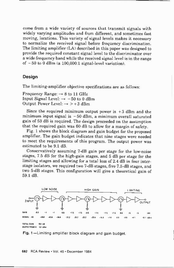
come from a wide variety of sources that transmit signals with widely varying amplitudes and from different, and sometimes fast moving, locations. This variety of signal levels makes it necessary to normalize the received signal before frequency discrimination. The limiting amplifier (LA) described in this paper was designed to provide the required constant signal level to the discriminator over a wide frequency band while the received signal level is in the range of - 50 to 0 dBm (a 100,000:1 signal -level variation).
Design
The limiting -amplifier objective specifications are as follows:
Frequency Range: -> 8 to 11 GHz Input Signal Level: - - 50 to 0 dBm Output Power Level: -> + 3 dBm
Since the required minimum output power is +3 dBm and the minimum input signal is - 50 dBm, a minimum overall saturated gain of 53 dB is required. The design proceeded on the assumption that the required gain was 60 dB to allow for a margin of safety.
Fig. 1 shows the block diagram and gain budget for the proposed amplifier. The gain budget indicates that nine stages were needed to meet the requirements of this program. The output power was estimated to be 9.1 dB.
Conservatively assuming 7 -dB gain per stage for the low -noise stages, 7.5 dB for the high -gain stages, and 5 dB per stage for the limiting stages and allowing for a total loss of 2.4 dB in four inter - stage isolators, we required two 7 -dB stages, five 7.5 -dB stages, and two 5 -dB stages. This configuration will give a theoretical gain of 59.1 dB.
INPUT
LOW NOISE
>- HIGH GAIN
GAIN -0.6 .7 .7 -0.6 .7.5 7.5 -06
>->- LIMITING
>---J OUTPUT
7.5 7.5 .7.6 -0.6 5 5 Inel
SIGNAL -50 -50.6 J0.6 -36.6 -77.1 -29.7 -22.2 -22.8 -15.3 -7.8 -0.3 -0.9 0.1 9.1
TOTAL GAIN 59.1 dB
OUTPUT POWER .9.1 dBm
Fig. 1-Limiting amplifier block diagram and gain budget.
682 RCA Review Vol. 45 December 1984
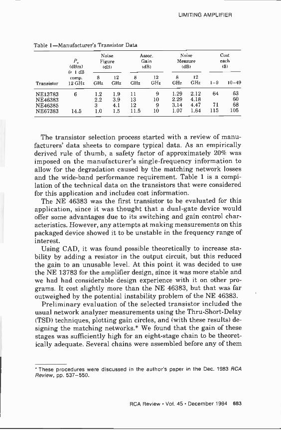
LIMITING AMPLIFIER
Table 1-Manufacturer's Transistor Data
Noise Assoc. Noise Cost Po Figure Gain Measure each
(dBm) (dB) (dB) (dB) (5) (á 1 dB
8 12 8 12 8 12 comp. Transistor 12 GHz GHz GHz GHz Gliz GHz GHz 1-9 10-49
NE13783 6 1.2 1.9 11 9 1.29 2.12 64 63 NE46383 2.2 3.9 13 10 2.29 4.18 60 NE46385 3 4.1 12 9 3.14 4.47 71 68 NE67383 14.5 1.0 1.5 11.5 10 1.07 1.64 115 105
The transistor selection process started with a review of manu- facturers' data sheets to compare typical data. As an empirically derived rule of thumb, a safety factor of approximately 20% was imposed on the manufacturer's single -frequency information to allow for the degradation caused by the matching network losses and the wide -band performance requirement. Table 1 is a compi- lation of the technical data on the transistors that were considered for this application and includes cost information.
The NE 46383 was the first transistor to be evaluated for this application, since it was thought that a dual -gate device would offer some advantages due to its switching and gain control char- acteristics. However, any attempts at making measurements on this packaged device showed it to be unstable in the frequency range of interest.
Using CAD, it was found possible theoretically to increase sta- bility by adding a resistor in the output circuit, but this reduced the gain to an unusable level. At this point it was decided to use the NE 13783 for the amplifier design, since it was more stable and we had had considerable design experience with it on other pro- grams. It cost slightly more than the NE 46383, but that was far outweighed by the potential instability problem of the NE 46383.
Preliminary evaluation of the selected transistor included the usual network analyzer measurements using the Thru-Short-Delay (TSD) techniques, plotting gain circles, and (with these results) de- signing the matching networks.' We found that the gain of these stages was sufficiently high for an eight -stage chain to be theoret- ically adequate. Several chains were assembled before any of them
These procedures were discussed in the author's paper in the Dec. 1983 RCA Review, pp. 537-550.
RCA Review Vol. 45 December 1984 683
were evaluated in the final system. It was there that we found that more gain would be required to provide an adequate margin at the - 50-dBm input power level. The additional gain took the form of an add-on housing containing a two -stage circuit carrier. This small unit was placed between the two larger housings.
Results
The overall response of the three -housing chain is shown in Fig. 2(a). As can be seen, with 3 volts on the drains of all of the tran- sistors, the amplifier was not limiting well at an input -signal level of - 50 dBm. Reducing the drain voltage to 2 volts on all four tran- sistor stages in the output housing produced the results shown in Fig. 2(b), where the amplifier was limited at the - 50 dBm level. This change in voltage also reduced the output -signal variation to 0.6 dB peak -to -peak as opposed to a 0.9 -dB peak -to -peak variation at 3 volts.
The response shown in Fig. 2(b), while smoother than that of Fig. 2(a), is not adequate for the system due to the remaining amplitude ripples, since the discriminator is very sensitive to small variations in signal amplitude. If there are two input signals very close to- gether, these variations could result in the same discriminator output voltage at two different input frequencies. The system then could not determine which frequency was actually being received.
The discriminator output voltage had a negative slope, i.e., de- creasing output with increasing frequency. The steeper the slope of the overall system frequency response (within limits), the better the differentiation between closely spaced frequencies. It was deter- mined that the system performance would be enhanced if the LA had an output power level versus frequency response that sloped in the same manner as the discriminator's.
The judicious placement of a long stub in the last amplifier stage produced the desired negative slope response from the LA chain. Various stub lengths were tried until an optimum configuration was found. If the stub length is too long, the amplifier output at the high -frequency end of the band is too low in power. If too short, the positive sloping portions of the response are not eliminated. Fig. 3 shows the LA's response to several different stub lengths.
The response of the final LA chain is shown in Fig. 4. The min- imum gain was 59 dB at the high end of the band and at least 63 dB at the low end. Over some portions of the band, the chain is limiting with input signals as low as -60 dBm.
684 RCA Review Vol. 45 December 1984
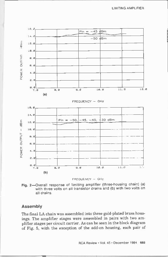
LIMITING AMPLIFIER
on
'4 0
2 0
'0 0
B 0
6 0
4 0
2 0
0. 0 7. 0
16. 0
14. 0
CO 12. 0
I 10. 0
/- 3
:.:
4 0
O d 2 0
0. 0 7. 0
Pin = -45 d Bm
-50 d Bm
(a)
B. 0 9. 0 10 0
FREQUENCY - GHz
11 2 12 0
Pin = -50, -45, -40, -30 dBm
(b)
B.0 9.0 10 0 11 0
FREQUENCY - GHz
Fig. 2-Overall response of limiting amplifier (three -housing chain) (a)
with three volts on all transistor drains and (b) with two volts on
all drains.
Assembly
The final LA chain was assembled into three gold-plated brass hous- ings. The amplifier stages were assembled in pairs with two am- plifier stages per circuit carrier. As can be seen in the block diagram of Fig. 5, with the exception of the add-on housing, each pair of
RCA Review Vol. 45 December 1984 685
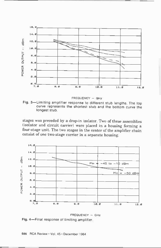
E
16 0
14 0
12 0
10 0
B 0
6 0
4 0
2 0
0. 0
--.---...:--:--___.-:-___ ` \_.--__ \
---.
_---_-----
-....
7. 0 8. 0 9. 0 10 0 11 0 12. 0
FREQUENCY - GHz
Fig. 3-Limiting amplifier response to different stub lengths. The top curve represents the shortest stub and the bottom curve the longest stub.
stages was preceded by a drop -in isolator. Two of these assemblies (isolator and circuit carrier) were placed in a housing forming a four -stage unit. The two stages in the center of the amplifier chain consist of one two -stage carrier in a separate housing.
16 0
14 0
CD 12 0
10
o- 8 0
o 6 0
cc
o t1
2
0.
0
1
Pin = -45 to -10 dBm
Pin = -50 dBrrt
o
7. 0 8. 0 9. 0 10 0
FREQUENCY - GHz
Fig. 4-Final response of limiting amplifier.
11 0 12 0
686 RCA Review Vol. 45 December 1984
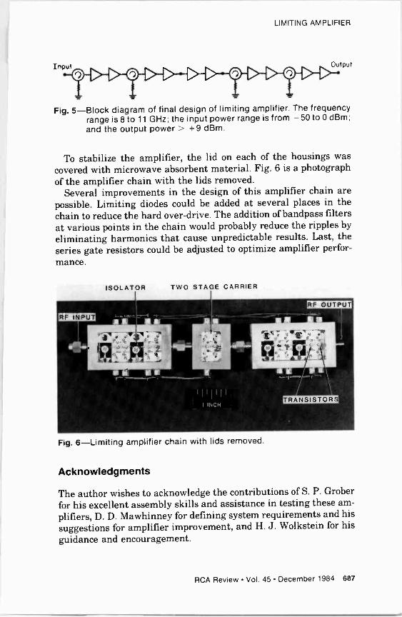
LIMITING AMPLIFIER
Input Output
Fig. 5-Block diagram of final design of limiting amplifier. The frequency range is 8 to 11 GHz; the input power range is from -50 to 0 dBm; and the output power > +9 dBm.
To stabilize the amplifier, the lid on each of the housings was
covered with microwave absorbent material. Fig. 6 is a photograph of the amplifier chain with the lids removed.
Several improvements in the design of this amplifier chain are possible. Limiting diodes could be added at several places in the chain to reduce the hard over -drive. The addition of bandpass filters at various points in the chain would probably reduce the ripples by
eliminating harmonics that cause unpredictable results. Last, the series gate resistors could be adjusted to optimize amplifier perfor- mance.
ISOLATOR TWO STAGE CARRIER
es, =--i +L...
I,-4-15- :rT-i c =c.Y
^ .§
]1 Y
I RANSISTORS
Fig. 6-Limiting amplifier chain with lids removed.
Acknowledgments
The author wishes to acknowledge the contributions of S. P. Grober for his excellent assembly skills and assistance in testing these am-
plifiers, D. D. Mawhinney for defining system requirements and his suggestions for amplifier improvement, and H. J. Wolkstein for his
guidance and encouragement.
RCA Review Vol. 45 December 1984 687
Patents Issued to RCA Inventors-Third Quarter 1984
July
N. W. Brackelmanns and W. Hulstrunk Fast Switching Transistor (4,460,913) M. K. Brown and K. S. Richard Rigid Cathode Support Structure for an In -Line Electron Gun Assembly (4,460,845) L. A. Christopher, G. A. Reitmeier, T. R. Smith and C. H. Strolle Window -Scanned Memory (4,460,958) J. C. Connolly and D. Botez Terraced Heterostructure Semiconductor Laser (4,461,008) S. L. Corsover, G. J. Ammon and C. W. Reno Multi -Beam Optical Record and Play- back Apparatus Having an Improved Beam Splitter (4,459,690) A. T. Crowley Phase Frequency Detector Using Shift Register (4,459,559) A. G. Dingwall Electronic Circuits and Structures Employing Enhancement and Depletion Type IGFETS (4,463,273) T. J. Faith, Jr., R. S. Irven and S. K. Plante Method for Mounting a Sapphire Chip on a Metal Base and Article Produced Thereby (4,457,976) I. Gorog Signal Pickup Cartridge (4,459,692) J. F. Hacke, A. J. Banks and L. J. Bazin Square -Wave Symmetry Corrector (4,461,962) J. R. Harford Integrated Circuit Overload Protection Device (4,463,369) J. E. Hicks Horizontal Output Transistor Protector Circuit (4,459,517) B. L. Hoffman Vacuum Gripping Apparatus (4,460,208) H. Huang and D. D. Mawhinney Monolithic Voltage Controlled Oscillator (4,458,215) K. C. Hudson Semiconductor Laser Scanning System (4,460,240) W. M. Janton Waveguide Tunable Oscillator Cavity Structure (4,459,564) L. A. Kaplan Power Amplifier Circuit Employing Field -Effect Power Transistors (4,463,318) E. F. Kujas Negative Hydrogen Electrode Comprising an Alloy of Palladium and Ruthenium (4,460,660) N. R. Landry and L. H. Yorinks Dispersion Correcting Waveguide (4,458,229) H. G. Lewis, Jr. Clock Generation Apparatus for a Digital Television System (4,463,371) C. C. Lim Piezoelectric Ultor Voltage Generator for a Television Receiver (4,459,505) J. Maa Patterning of Submicrometer Metal Silicide Structures (4,460,435) R. J. McIntyre and P. P. Webb Avalanche Photodiode Array (4,458,260) R. J. McIntyre and P. P. Webb Silicon Avalanche Photodiode With Low Keff (4,463,368) M. L. McNeely VideoDisc Preform and Method of Making a Disc Therefrom (4,460,656) T. D. Michaelis Encoder Controlled Apparatus for Dynamic Braking (4,460,857) R. P. Parker Kinescope Black Level Current Sensing Apparatus (4,463,385) S. Pearlman Reducing Glare from the Surface of a Glass Viewing Window (4,460,621) F. R. Ragland, Jr. Color Picture Tube Having Improved Temperature Compensating Support for a Mask -Frame Assembly (4,460,843) J. H. Rainey and C. D. Boltz, Jr. VideoDisc Caddy (274,905) M. D. Ross Noise Reduction Circuitry for Audio Signals (4,462,048) G. Samuels Apparatus for Spraying a Liquid on a Spinning Surface (4,457,259) O. H. Schade, Jr. Trimming Circuits for Precision Amplifier (4,462,002) E. T. Schmitt, H. R. Ronan, Jr. and M. R. Schuler Fixture for Testing Semiconductor Devices (4,460,868) A. C. Schroeder Sampling Arrangement for a Television Ghost Signal Cancellation System (4,458,269) D. Stavitsky and E. A. Beres Injection Molding Apparatus (4,462,780) C. H. Strolle Memory Scanning Address Generator (4,462,024) R. L. Turner and R. E. Jennings Rack for Transporting Recorded Discs (4,461,386) G. J. Whitley Apparatus for Securing a Component to a Printed Circuit Board (4,462,435)
RCA Review Vol. 45 December 1984 688
G. J. Whitley Apparatus for Detecting the Presence of Components on a Printed Circuit Board (4,463,310) K. J. Yakmovitz Television Receiver and Test Set Voltage Analyzer (4,459,551)
August
I. Abeyta Circuit for Coupling Signals to or from a Circuit Under Test (4,465,971) A. R. Balaban and S. A. Steckler Low Frequency Digital Comb Filter System (4,464,675) S. Bloom CRT With Quadrupolar-Focusing Color -Selection Structure (4,464,601) B. F. Bogner Radial Transmission Cancellation Device (4,466,090) E. A. Brauer Stylus Cleaner Pad Orientation in Disc Record Player (4,464,742) M. S. Chartier Digital Gain Control System (4,464,723) A. T. Crowley and R. M. Lisowski Universal Digital Frequency Synthesizer Using Signal Side Band Techniques (4,464,638) A. T. Crowley Phase Locked Loop Frequency Synthesizer Including Fractional Dig- ital Frequency Divider (4,468,632) W. V. Fitzgerald, Jr. Regulated Power Supply Incorporating a Power Transformer Having a Tightly Coupled Supplemental Power Transfer Winding (4,466,051) M. T. Gale and K. H. Knop Dynamic Accuracy X -Y Positioning Table for Use in a
High Precision Light -Spot Writing System (4,464,030) S. B. Goldberg Amplitude Control Apparatus (4,468,631) I. Gorog VideoDisc Caddy (4,463,850) B. Greenstein Method and Apparatus for Quantitatively Evaluating the Soldering Properties of a Wave Soldering System (4,467,638) P. E. Haferl Horizontal Drive and Nonlinearity Correction Circuit (4,468,593) L. A. Harwood and R. L. Shanley, 2nd Amplifier Incorporating Gain Distribution Control for Cascaded Amplifying Stages (4,464,633) J. P. Hasili Line Cathode Heating and Protection Circuit (4,464,611) J. H. Helm VideoDisc Player Having Turntable Retention Mechanism (4,464,744) H. Huang, M. Kumar and F. N. Sechi Predistortion Circuit for a Power Amplifier (4,465,980) L. M. Hughes VideoDisc Player Having Door Lock Mechanism (4,467,466) F. S. Krufka System and Method of Accurately Controlling the Electrode Voltage of a Capacitive Load (4,464,556) W. J. Maddox System for Applying a High Voltage Source to a CRT Through a
Capacitive Load (4,467,224) J. R. Nelson, W. K. Wissing and V. S. Dunn Formulation of Electrically Conductive Plastics (4,465,616) W. S. Pike Adaptive Control Signal Filter for Audio Signal Expander (4,465,981) A. N. Prabhu and K. W. Hang Indium Oxide Resistor Inks (4,467,009) D. H. Pritchard Television Signal Filtering System (4,466,016) J. J. Prusak and B. P. Patel VideoDisc Caddy (4,463,849) G. A. Reitmeier Adaptive Television Signal Estimator (4,464,686) I. G. Ritzman Method of Removing a Glass Backing Plate from One Major Surface of a Semiconductor Wafer (4,465,549) H. G. Scheible and J. B. Berkshire Wave Soldering Apparatus and Method (4,463,891) L. N. Schiff and S. Freeman Time Window Key System for Video Scrambling (4,464,678) R. E. Schlack and K. S. Richard Cathode Support Structure for an In -Line Electron Gun Assembly (4,468,588) R. G. Stewart and A. G. Dingwall Memory System With Redundancy for Error Avoid- ance (4,464,754) R. G. Stewart and A. G. Dingwall Memory System With Error Detection and Cor- rection (4,464,755) C. R. Thompson Digital Recording of Television Components With Improved Tran- sition Spacing (4,464,683) J. R. Tower Multi -Chip Imager (4,467,342) R. L. Turner and J. J. Prusak Apparatus for Manufacturing Disc Record Package (4,465,453) R. A. Wargo Method and Apparatus for Operating a Microprocessor in Synchronism With a Video Signal (4,464,679)
689 RCA Review Vol. 45 December 1984
R. A. Wargo and S. S. Perlman Automatic Color Burst Magnitude Control for a Digital Television Receiver (4,466,015) R. A. Wasson Fail -Safe Sensor Circuit (4,467,386) C. A. Weaver Apparatus for Attaching a Matrix to an Electroforming Device and Method Therefor (4,468,290) B. A. Whipple and V. S. Dunn Method for Preparing a Molding Composition (4,465,617) G. J. Whitley and M. Rayl Component Lead Bending Apparatus (4,464,829) L. P. Wilbur, Jr. and M. H. Wardell, Jr. Color Selection Electrode Mounting Struc- ture Having an Off -Set Washer (4,467,242) Y. Yarnitsky and A. Livny JIG for Use in Machining Stylus Blanks (4,466,555)
September
S. Bloom and E. F. Hockings Method of Fabricating a Metalized Electrode Assembly (4,470,822) T. V. Bolger Color Channel Signal -To -Noise Improvement in Digital Television (4,472,733) R. A. Dischert and J. M. Walter Multiplier for Digital Video Signals Using a Cascade of Signal -Selectable Memories (4,470,125) R. A. Dischert Television Camera Mechanical Apparatus Driven by Recorder Motor (4,471,388) D. J. Erber and G. D. Ross, Jr. VideoDisc Player (275,668) A. W. Fisher Local Oxidation of Silicon Substrate Using LPCVD Silicon Nitride (4,472,459) R. E. Flory and C. R. Thompson Chrominance Channel Bandwidth Modification System (4,472,746) L. P. Fox and L. A. Dimarco Conductive Molding Composition and Discs Therefrom (4,472,295) P. D. Griffis Frequency Translation Phase -Locked Loop Television Sound Detection System Utilizing a Single IF Amplifier (4,470,070) D. K. Guhn Phase Lock Loss Detector (4,473,805) D. F. Hakala Process for Treating High -Density Information Disc Recording Sub- strates (4,469,563) D. V. Henry Modular Welding Apparatus (4,473,734) K. G. Hernqvist CRT With Internal Neck Coating for Suppressing Arcing Therein (4,473,774) P. M. Heyman Method for Intaglio Printing and Selectively Alterable Inking Plate Therefor (4,473,008) D. M. Hoffman Process for Radiation Free Electron Beam Deposition (4,472,453) R. H. Huck, F. R. Nyman and D. A. Berry VideoDisc Processing (4,472,337) R. H. (sham Bidirectional Interface (4,471,243) M. F. Kaminsky Charge Time Start Control for Interconnect PABX (4,472,600) L. A. Kaplan Output Protection Circuit for Preventing a Reverse Current (4,471,237) T. F. Kirschner VideoDisc Player Having Carriage Locking Mechanism (4,471,478) M. Kumar and L. C. Upadhyayula Power Divider/Combiner Circuit as for Use in a Switching Matrix (4,472,691) H. G. Lewis, Jr. Reduced Data Rate Digital Comb Filter (4,470,069) A. Miller Method of Cleaving a Crystal to Produce a High Optical Quality Corner (4,469,500) D. B. O'Leary VideoDisc Player (275,566) J. I. Pankove and M. L. Tarng Method and Structure for Passivating a PN Junction (4,473,597) C. E. Profera and H. H. Soule, Jr. Phase Reconfigurable Beam Antenna System (4,471,361) J. J. Prusak Apparatus for Manufacturing a Disc Record Package (4,470,795) G. A. Reitmeier Adaptive Error Concealment Using Horizontal Information Deter- mination from Adjacent Lines (4,470,065) A. E. Rindal Television Sound Detection System Using a Frequency Translation Phase -Locked Loop (4,470,071) D. J. Sauer Pipe -Lined CCD Analog -To -Digital Converter (4,471,341) S. A. Steckler and A. R. Balaban Current Supplying Circuit as for an Oscillator (4,471,326)
RCA Review Vol. 45 December 1984 690
i
1
C. H. Strolle Phantom Raster Generating Apparatus Scanning TV Image Memory in Angular and Orthogonal Coordinates (4,471,349) L. A. Torrington Disc Record Player Having Carriage Locking Apparatus (4,472,796) I. T. Wacyk, R. G. Stewart and A. G. Dingwall Memory System With Error Storage (4,472,805) F. S. Wendt Self -Regulating Saturating Core Television Receiver Power Supply (4,471,271) L. K. White and M. Popov Preparation of Organic Layers for Oxygen Etching (4,470,871) M. L. Whitehurst Method for the Manufacture of Capacitive Electronic Discs (4,470,940) R. E. Wilson Control Circuit for Telephone Receiver and Transmitter (4,472,601) C. P. Wu, G. L. Schnable, R. E. Stricker and B. W. Lee Method of Making a Semi- conductor Device to Improve Conductivity of Amorphous Silicon Films (4,472,210) G. S. Zorbalas Automatic Scan Tracking With Ringing Control (4,471,392)
691 RCA Review Vol. 45 December 1984
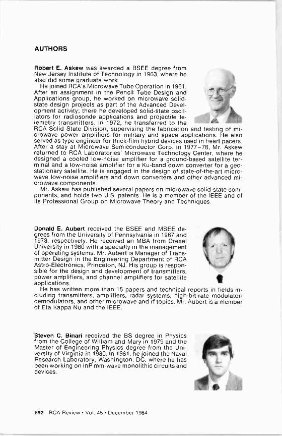
AUTHORS
Robert E. Askew was awarded a BSEE degree from New Jersey Institute of Technology in 1963, where he also did some graduate work.
He joined RCA's Microwave Tube Operation in 1961. After an assignment in the Pencil Tube Design and Applications group, he worked on microwave solid- state design projects as part of the Advanced Devel- opment activity; there he developed solid-state oscil- lators for radiosonde applications and projectile te- lemetry transmitters. In 1972, he transferred to the RCA Solid State Division, supervising the fabrication and testing of mi- crowave power amplifiers for military and space applications. He also served as type engineer for thick -film hybrid devices used in heart pacers. After a stay at Microwave Semiconductor Corp. in 1977-78, Mr. Askew returned to RCA Laboratories' Microwave Technology Center, where he designed a cooled low -noise amplifier for a ground -based satellite ter- minal and a low -noise amplifier for a Ku -band down converter for a geo- stationary satellite. He is engaged in the design of state-of-the-art micro- wave low -noise amplifiers and down converters and other advanced mi- crowave components.
Mr. Askew has published several papers on microwave solid-state com- ponents, and holds two U.S. patents. He is a member of the IEEE and of its Professional Group on Microwave Theory and Techniques.
Donald E. Aubert received the BSEE and MSEE de- grees from the University of Pennsylvania in 1967 and 1973, respectively. He received an MBA from Drexel University in 1980 with a specialty in the management of operating systems. Mr. Aubert is Manager of Trans- mitter Design in the Engineering Department of RCA /! Astro -Electronics, Princeton, NJ. His group is respon- sible for the design and development of transmitters, power amplifiers, and channel amplifiers for satellite applications.
He has written more than 15 papers and technical reports in fields in- cluding transmitters, amplifiers, radar systems, high -bit -rate modulator/ demodulators, and other microwave and rf topics. Mr. Aubert is a member of Eta Kappa Nu and the IEEE.
'Steven C. Binari received the BS degree in Physics from the College of William and Mary in 1979 and the Master of Engineering Physics degree from the Uni- versity of Virginia in 1980. In 1981, he joined the Naval Research Laboratory, Washington, DC, where he has beers working on InP mm -wave monolithic circuits and devices.
Li
ar
692 RCA Review Vol. 45 December 1984
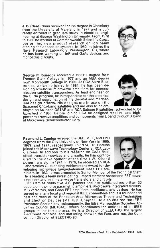
J. B. (Brad) Boos received the BS degree in Chemistry from the University of Maryland in 1977 and is cur- rently enrolled in graduate study in electrical engi- neering at George Washington University. From 1978 to 1980 he worked at Commonwealth Scientific Corp., performing new product research on ion beam etching and deposition systems. In 1980, he joined the Naval Research Laboratory, Washington, DC, where he has been working on InP and GaAs devices and monolithic circuits.
George R. Busacca received a BSEET degree from Trenton State College in 1977 and an MBA degree from Monmouth College in 1983. At RCA Astro -Elec- tronics, which he joined in 1981, he has been de- signing low -noise microwave amplifiers for commu- nication satellite transponders. As lead engineer on :ate the CLNA program, he is responsible for the electrical design and coordination of the thermal and mechan- ', ical design efforts. His designs are in use on the Spacenet C/Ku-band satellites and are also to be em- ployed on Ku -band GSTAR and RCA Satcom K satellites, scheduled to be launched in 1985. Before joining RCA he designed medium- and high - power microwave amplifiers and components from L band through X band at Microwave Semiconductor Corp.
4;0*:11-~
Raymond L. Camisa received the BEE, MEE, and PhD degrees from the City University of New York in 1965, 1969, and 1974, respectively. In 1974, Dr. Camisa joined the Microwave Technology Center at RCA Lab- oratories.
,w In addition to his research on GaAs field- l p,
effect -transistor devices and circuits, he has contrib- k - `r`
uted to the development of the first 1-W, X -band power transistor in 1974. In 1979, he received an RCA Laboratories Outstanding Achievement Award for de- veloping microwave lumped -element GaAs FET am- plifiers. In 1983 he was promoted to Senior Member of the Technical Staff. He is leading a team investigating lumped -element broadband FET power amplifiers and millimeter -wave transistors and circuits.
Dr. Camisa holds five U.S. patents and has published more than 20 papers on low -noise parametric amplifiers, microwave integrated circuits, MIS varactors, and GaAs FET amplifiers, oscillators, and devices. He has served on many local and regional IEEE committees and is a founder and past chairman of the Princeton Area Microwave Theory and Techniques and Electron Devices (MTT/ED) Chapter. He also chaired the IEEE Princeton Section and, subsequently, the IEEE Metropolitan Societies Ac- tivities Council (METSAC), which coordinates the activities of all IEEE groups in the tri-state area. He is a Director of ELECTRO, the largest electronics technical and marketing show in the East, and was the Con- vention Director of ELECTRO 83.
RCA Review Vol. 45 December 1984 693
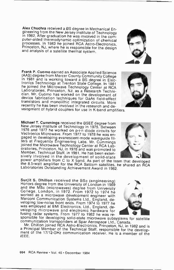
Alex Chuchra received a BS degree in Mechanical En- gineering from the New Jersey Institute of Technology in 1982. After graduation he was involved in the com- puter -aided thermodynamic optimization of chemical processes. In 1983 he joined RCA Astro -Electronics, Princeton, NJ, where he is responsible for the design and analysis of a satellite thermal system.
Frank P. Cuomo earned an Associate Applied Science (AAS) degree from Mercer County Community College in 1981 and is working toward a BS degree in Elec- tronics Technology at Trenton State College. In 1981 he joined the Microwave Technology Center at RCA Laboratories, Princeton, NJ, as a Research Techni- cian. Mr. Cuomo has worked on the development of device fabrication techniques for GaAs field-effect transistors and monolithic integrated circuits. More recently he has been involved in the research and de- velopment of hybrid couplers for use in K -band amplifiers.
Michael T. Cummings received the BSEE degree from New Jersey Institute of Technology in 1975. Between 1976 and 1977 he worked on p -i -n diode circuits for Vectronics Microwave. From 1977 to 1978 he was en- gaged in developing evanescent -mode waveguide fil- ters at Frequency Engineering Labs. Mr. Cummings joined the Microwave Technology Center at RCA Lab- oratories, Princeton, NJ, in 1978 and was promoted to Member, Technical Staff, in 1981. He has been exten sively involved in the development of solid-state power amplifiers from C to X band. As part of the team that developed the 8.5 -watt amplifier for the RCA Satcom satellites, he shared an RCA Laboratories Outstanding Achievement Award in 1982.
,
Surjit S. Dhillon received the BSc (engineering) Honors degree from the University of London in 1969 and the MSc (microwaves) degree from University Í College, London, ín 1972. From 1972 to 1974 he worked as a microwave development engineer with Marconi Communication Systems Ltd., England, de- veloping low -noise front ends. From 1974 to 1977 he was employed at EMI Electronics, Ltd., England, de- veloping microwave and electronic hardware for11111 fusing radar systems. From 1977 to 1982 he was re- sponsible for developing solid-state microwave subsystems for satellite communication transponders at Spar Aerospace Ltd., Canada.
Mr. Dhillon joined RCA Astro -Electronics, Princeton, NJ, in 1982 and is a Principal Member of the Technical Staff, responsible for the develop- ment of the 17/12-GHz communication receiver. He is a member of the IEEE.
694 RCA Review Vol. 45 December 1984
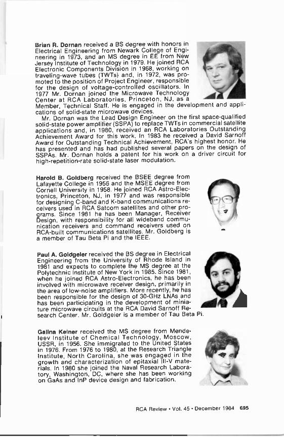
Brian R. Dornan received a BS degree with honors in Electrical Engineering from Newark College of Engi- neering in 1973, and an MS degree in EE from New Jersey Institute of Technology in 1979. He joined RCA Electronic Components Division in 1968, working on traveling -wave tubes (TWTs) and, in 1972, was pro- moted to the position of Project Engineer, responsible . -- for the design of voltage -controlled oscillators. In ` f 1977 Mr. Dornan joined the Microwave Technology Center at RCA Laboratories, Princeton, NJ, as a
Member, Technical Staff. He is engaged in the development and appli- cations of solid-state microwave devices.
Mr. Dornan was the Lead Design Engineer on the first space -qualified solid-state power amplifier (SSPA) to replace TWTs in commercial satellite applications and, in 1980, received an RCA Laboratories Outstanding Achievement Award for this work. In 1983 he received a David Sarnoff Award for Outstanding Technical Achievement, RCA's highest honor. He
has presented and has had published several papers on the design of SSPAs. Mr. Dornan holds a patent for his work on a driver circuit for high -repetition -rate solid-state laser modulation.
Harold B. Goldberg. received the BSEE degree from Lafayette College in 1956 and the MSEE degree from Cornell University in 1958. He joined RCA Astro -Elec- tronics, Princeton, NJ, in 1977 and was responsible for designing C -band and K -band communications re- ceivers used in RCA Satcom satellites and other pro- grams. Since 1981 he has been Manager, Receiver Design, with responsibility for all wideband commu- nication receivers and command receivers used on RCA -built communications satellites. Mr. Goldberg is a member of Tau Beta Pi and the IEEE.
Paul A. Goldgeier received the BS degree in Electrical Engineering from the University of Rhode Island in 1981 and expects to complete the MS degree at the Polytechnic Institute of New York in 1985. Since 1981, when he joined RCA Astro -Electronics, he has been involved with microwave receiver design, primarily in the area of low -noise amplifiers. More recently, he has been responsible for the design of 30-GHz LNAs and has been participating in the development of minia- ture microwave circuits at the RCA David Sarnoff Re- search Center. Mr. Goldgeier is a member of Tau Beta
Galina Kelner received the MS degree from Mende- leev Institute of Chemical Technology, Moscow, USSR, in 1956. She immigrated to the United States in 1976. From 1976 to 1980, at the Research Triangle Institute, North Carolina, she was engaged in the growth and characterization of epitaxial III -V mate- rials. In 1980 she joined the Naval Research Labora- tory, Washington, DC, where she has been working on GaAs and InP device design and fabrication.
.:.
RCA Review Vol. 45 December 1984 695
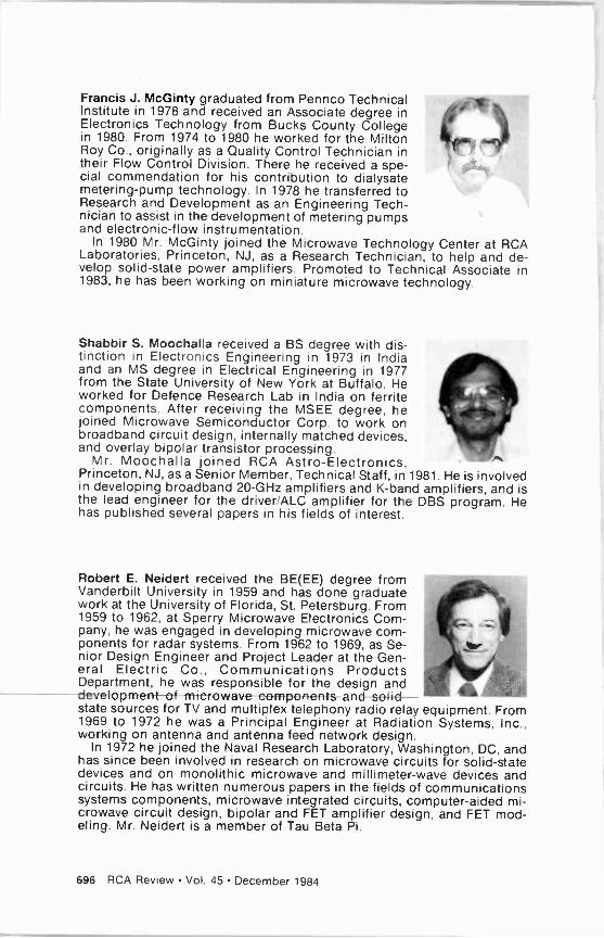
Francis J. McGinty graduated from Pennco Technical t Institute in 1978 and received an Associate degree in Electronics Technology from Bucks County College in 1980. From 1974 to 1980 he worked for the Milton ' -
Roy Co., originally as a Quality Control Technician in m
their Flow Control Division. There he received a spe- cial commendation for his contribution to dialysate metering -pump technology. In 1978 he transferred to Research and Development as an Engineering Tech- nician to assist in the development of metering pumps and electronic -flow instrumentation.
In 1980 Mr. McGinty joined the Microwave Technology Center at RCA Laboratories, Princeton, NJ, as a Research Technician, to help and de- velop solid-state power amplifiers. Promoted to Technical Associate in 1983, he has been working on miniature microwave technology.
Shabbir S. Moochalla received a BS degree with dis- tinction in Electronics Engineering in 1973 in India and an MS degree in Electrical Engineering in 1977 from the State University of New York at Buffalo. He worked for Defence Research Lab in India on ferrite components. After receiving the MSEE degree, he joined Microwave Semiconductor Corp. to work on broadband circuit design, internally matched devices, and overlay bipolar transistor processing.
Mr. Moochalla joined RCA Astro -Electronics, Princeton, NJ, as a Senior Member, Technical Staff, in 1981. He is involved in developing broadband 20-GHz amplifiers and K -band amplifiers, and is the lead engineer for the driver/ALC amplifier for the DBS program. He has published several papers in his fields of interest.
Robert E. Neidert received the BE(EE) degree from Vanderbilt University in 1959 and has done graduate work at the University of Florida, St. Petersburg. From 1959 to 1962, at Sperry Microwave Electronics Com- pany, he was engaged in developing microwave corn- G
ponents for radar systems. From 1962 to 1969, as Se- nior Design Engineer and Project Leader at the Gen-
v eral Electric Co., Communications Products . ',= .
Department, he was responsible for the design and '' -ti *f developmenT-of microwave components -and solid- state sources for TV and multiplex telephony radio relay equipment. From 1969 to 1972 he was a Principal Engineer at Radiation Systems, Inc., working on antenna and antenna feed network design.
In 1972 he joined the Naval Research Laboratory, Washington, DC, and has since been involved in research on microwave circuits for solid-state devices and on monolithic microwave and millimeter -wave devices and circuits. He has written numerous papers in the fields of communications systems components, microwave integrated circuits, computer -aided mi- crowave circuit design, bipolar and FET amplifier design, and FET mod- eling. Mr. Neidert is a member of Tau Beta Pi.
696 RCA Review Vol. 45 December 1984
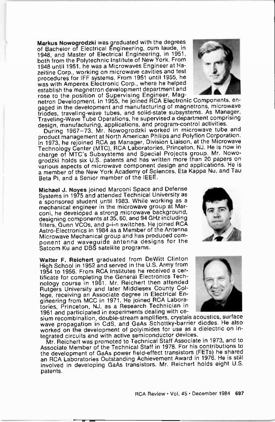
Markus Nowogrodzki was graduated with the degrees of Bachelor of Electrical Engineering, cum laude, in 1948, and Master of Electrical Engineering, in 1951, 4 both from the Polytechnic Institute of New York. From 1948 until 1951, he was a Microwaves Engineer at Ha- - '
zeltine Corp., working on microwave cavities and test procedures for IFF systems. From 1951 until 1955, he - was with Amperex Electronic Corp., where he helped establish the magnetron development department and Ai, rose to the position of Supervising Engineer, Mag- netron Development. In 1955, he joined RCA Electronic Components, en- gaged in the development and manufacturing of magnetrons, microwave triodes, traveling -wave tubes, and solid-state subsystems. As Manager, Traveling -Wave Tube Operations, he supervised a department comprising design, manufacturing, applications, and program -control activities.
During 1967-73, Mr. Nowogrodzki worked in microwave tube and product management at North American Philips and Polyflon Corporation. In 1973, he rejoined RCA as Manager, Division Liaison, at the Microwave Technology Center (MTC), RCA Laboratories, Princeton, NJ. He is now in
charge of MTC's Subsystems and Special Projects group. Mr. Nowo- grodzki holds six U.S. patents and has written more than 20 papers on various aspects of microwave component design and applications. He is
a member of the New York Academy of Sciences, Eta Kappa Nu, and Tau
Beta Pi, and a Senior member of the IEEE.
Michael J. Noyes joined Marconi Space and Defense Systems in 1975 and attended Technical University as a sponsored student until 1983. While working as a
mechanical engineer in the microwave group at Mar- coni, he developed a strong microwave background, designing components at 35, 60, and 94 GHz including filters, Gunn VCOs, and p -i -n switches. He joined RCA Astro -Electronics in 1984 as a Member of the Antenna Microwave Mechanical group and has produced com- ponent and waveguide antenna designs for the Satcom Ku and DBS satellite programs.
Walter F. Reichert graduated from DeWitt Clinton High School in 1952 and served in the U.S. Army from 1954 to 1956. From RCA Institutes he received a cer-
k°*"."'
tificate for completing the General Electronics Tech- nology course in 1961. Mr. Reichert then attended Rutgers University and later Middlesex County Col- lege, receiving an Associate degree in Electrical En- gineering from MCC in 1971. He joined RCA Labora- tories, Princeton, NJ, as a Research Technician in
V 1961 and participated in experiments dealing with ce- sium recombination, double -stream amplifiers, crystals acoustics, surface wave propagation in CdS, and GaAs Schottky -barrier diodes. He also worked on the development of polyimides for use as a dielectric on in-
tegrated circuits and with active semiconductor devices. Mr. Reichert was promoted to Technical Staff Associate in 1973, and to
Associate Member of the Technical Staff in 1978. For his contributions to the development of GaAs power field-effect transistors (FETs) he shared an RCA Laboratories Outstanding Achievement Award in 1976. He is still involved in developing GaAs transistors. Mr. Reichert holds eight U.S.
patents.
w
#1?
RCA Review Vol. 45 December 1984 697
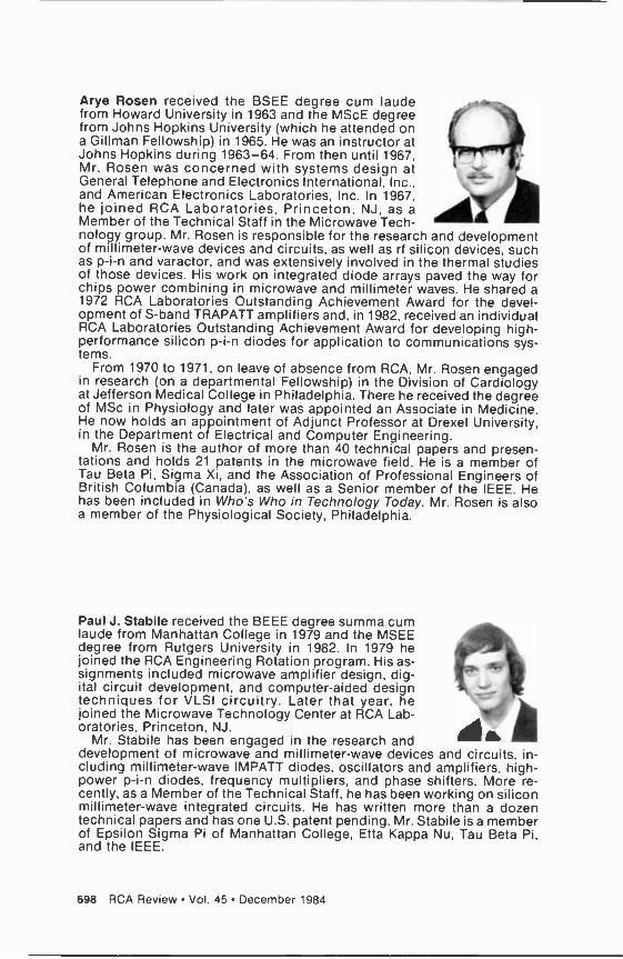
Arye Rosen received the BSEE degree cum laude from Howard University in 1963 and the MScE degree from Johns Hopkins University (which he attended on a Gillman Fellowship) in 1965. He was an instructor at Johns Hopkins during 1963-64. From then until 1967, !!_ : r Mr. Rosen was concerned with systems design at General Telephone and Electronics International, Inc., and American Electronics Laboratories, Inc. In 1967, ''- he joined RCA Laboratories, Princeton, NJ, as a Member of the Technical Staff in the Microwave Tech- nology group. Mr. Rosen is responsible for the research and development of millimeter -wave devices and circuits, as well as rf silicon devices, such as p -i -n and varactor, and was extensively involved in the thermal studies of those devices. His work on integrated diode arrays paved the way for chips power combining in microwave and millimeter waves. He shared a 1972 RCA Laboratories Outstanding Achievement Award for the devel- opment of S -band TRAPATT amplifiers and, in 1982, received an individual RCA Laboratories Outstanding Achievement Award for developing high- performance silicon p -i -n diodes for application to communications sys- tems.
From 1970 to 1971, on leave of absence from RCA, Mr. Rosen engaged in research (on a departmental Fellowship) in the Division of Cardiology at Jefferson Medical College in Philadelphia. There he received the degree of MSc in Physiology and later was appointed an Associate in Medicine. He now holds an appointment of Adjunct Professor at Drexel University, in the Department of Electrical and Computer Engineering.
Mr. Rosen is the author of more than 40 technical papers and presen- tations and holds 21 patents in the microwave field. He is a member of Tau Beta Pi, Sigma Xi, and the Association of Professional Engineers of British Columbia (Canada), as well as a Senior member of the IEEE. He has been included in Who's Who in Technology Today. Mr. Rosen is also a member of the Physiological Society, Philadelphia.
Paul J. Stabile received the BEEE degree summa cum laude from Manhattan College in 1979 and the MSEE degree from Rutgers University in 1982. In 1979 he joined the RCA Engineering Rotation program. His as- signments included microwave amplifier design, dig- ital circuit development, and computer -aided design k techniques for VLSI circuitry. Later that year, he joined the Microwave Technology Center at RCA Lab- oratories, Princeton, NJ.
Mr. Stabile has been engaged in the research and development of microwave and millimeter -wave devices and circuits, in- cluding millimeter -wave IMPATT diodes, oscillators and amplifiers, high - power p -i -n diodes, frequency multipliers, and phase shifters. More re- cently, as a Member of the Technical Staff, he has been working on silicon millimeter -wave integrated circuits. He has written more than a dozen technical papers and has one U.S. patent pending. Mr. Stabile is a member of Epsilon Sigma Pi of Manhattan College, Etta Kappa Nu, Tau Beta Pi, and the IEEE.
698 RCA Review Vol. 45 December 1984
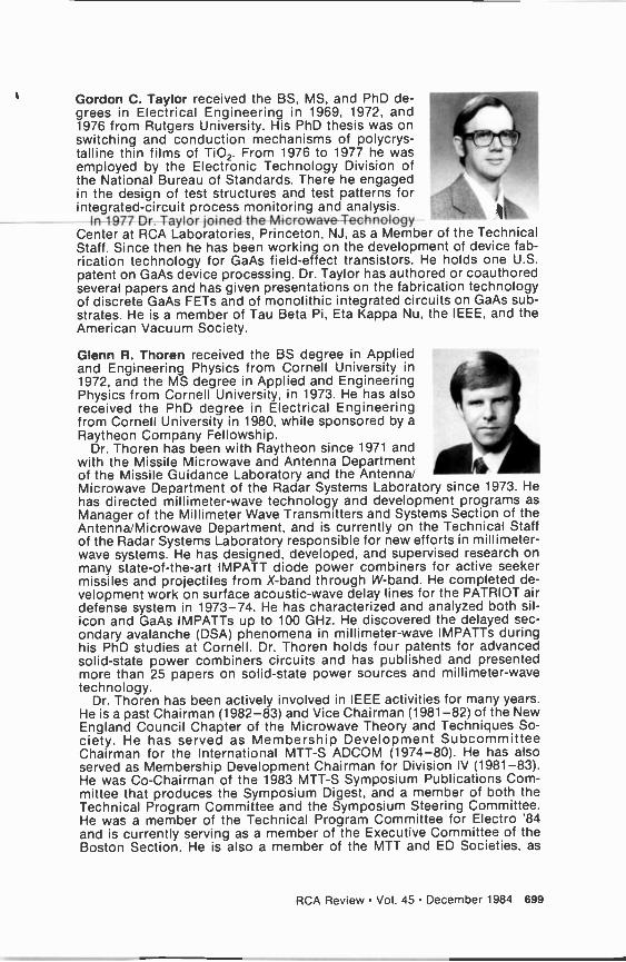
Gordon C. Taylor received the BS, MS, and PhD de- grees in Electrical Engineering in 1969, 1972., and 1976 from Rutgers University. His PhD thesis was on switching and conduction mechanisms of polycrys- talline thin films of TiO2. From 1976 to 1977 he was employed by the Electronic Technology Division of the National Bureau of Standards. There he engaged in the design of test structures and test patterns for integrated -circuit process monitoring and analysis.
In -1-977 Dr: Taylor joined the Microwave Technology- Center at RCA Laboratories, Princeton, NJ, as a Member of the Technical Staff. Since then he has been working on the development of device fab- rication technology for GaAs field-effect transistors. He holds one U.S. patent on GaAs device processing. Dr. Taylor has authored or coauthored several papers and has given presentations on the fabrication technology of discrete GaAs FETs and of monolithic integrated circuits on GaAs sub- strates. He is a member of Tau Beta Pi, Eta Kappa Nu, the IEEE, and the American Vacuum Society.
Glenn R. Thoren received the BS degree in Applied and Engineering Physics from Cornell University in 1972, and the MS degree in Applied and Engineering Physics from Cornell University, in 1973. He has also received the PhD degree in Electrical Engineering from Cornell University in 1980, while sponsored by a
Raytheon Company Fellowship. Dr. Thoren has been with Raytheon since 1971 and
with the Missile Microwave and Antenna Department of the Missile Guidance Laboratory and the Antenna Microwave Department of the Radar Systems Laboratory since 1973. He has directed millimeter -wave technology and development programs as Manager of the Millimeter Wave Transmitters and Systems Section of the Antenna/Microwave Department, and is currently on the Technical Staff of the Radar Systems Laboratory responsible for new efforts in millimeter - wave systems. He has designed, developed, and supervised research on many state-of-the-art IMPATT diode power combiners for active seeker missiles and projectiles from X -band through W -band. He completed de- velopment work on surface acoustic -wave delay lines for the PATRIOT air defense system in 1973-74. He has characterized and analyzed both sil- icon and GaAs IMPATTs up to 100 GHz. He discovered the delayed sec- ondary avalanche (DSA) phenomena in millimeter -wave IMPATTs during his PhD studies at Cornell. Dr. Thoren holds four patents for advanced solid-state power combiners circuits and has published and presented more than 25 papers on solid-state power sources and millimeter -wave technology.
Dr. Thoren has been actively involved in IEEE activities for many years. He is a past Chairman (1982-83) and Vice Chairman (1981-82) of the New England Council Chapter of the Microwave Theory and Techniques So- ciety. He has served as Membership Development Subcommittee Chairman for the International MIT -S ADCOM (1974-80). He has also served as Membership Development Chairman for Division IV (1981-83). He was Co -Chairman of the 1983 MTT-S Symposium Publications Com- mittee that produces the Symposium Digest, and a member of both the Technical Program Committee and the Symposium Steering Committee. He was a member of the Technical Program Committee for Electro '84 and is currently serving as a member of the Executive Committee of the Boston Section. He is also a member of the MTT and ED Societies, as
RCA Review Vol. 45 December 1984 699
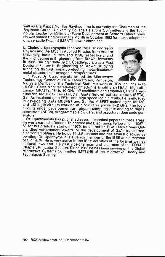
well as Eta Kappa Nu. For Raytheon, he is currently the Chairman of the Raytheon -Cornell University College Relations Committee and the Tech- nology Leader for Millimeter Wave Development at Bedford Laboratories. He was named Engineer of the Month in October 1982 for the development of a versatile W -band IMPATT power combiner.
L. Chainulu Upadhyayula received the BSc degree in Physics and the MSc in Applied Physics from Andhra University, India, in 1955 and 1958, respectively, and the PhD degree in Engineering from Brown University in 1968. During 1968-69 Dr. Upadhyayula was a Post Doctoral Fellow in Engineering at Brown, studying tunneling through superconducting metal -insulator- V metal structures at cryogenic temperatures.
In 1969, Dr. Upadhyayula joined the Microwave Technology Center at RCA Laboratories, Princeton, NJ, as a Member of the Technical Staff. His work at RCA includes 4- to 16-GHz GaAs transferred -electron (Gunn) amplifiers (TEAs), high -effi- ciency IMPATTs, 18- to 40-GHz InP oscillators and amplifiers, transferred - electron logic devices (TELDs), GaAs field-effect transistors (FETs), GalnAs insulated -gate FETs, and high-speed logic circuits. He is engaged in developing GaAs MESFET and GalnAs MISFET technologies for MSI and LSI logic circuits working at clock rates above 1-2 GHz. The logic circuits under development are gigabit -sampling rate analog -to -digital converters (ADCs), programmable dividers, and pseudorandom code gen- erators.
Dr. Upadhyayula has published several technical papers in these areas. He was awarded a General Telephone and Electronics Fellowship in 1967- 68 for his graduate study. In 1970, he shared an RCA Laboratories Out- standing Achievement Award for the development of GaAs transferred - electron amplifiers. He holds 14 U.S. patents and has several disclosures pending. Dr. Upadhyayula is a Senior member of the IEEE and a member of Sigma Xi. He is very active in the IEEE activities at the local as well as national level and is a past vice-chairman and chairman of the ED/MTT Chapter, Princeton Section. Since 1983 he has been serving on the Digital Microwave Systems Committee (MTTS-9) of the Microwave Theory and Techniques Society.
700 RCA Review Vol. 45 December 1984

Index, Volume 45, 1984
March
3 PIN-FET Receiver for Fiber Optics S. A. Siegel and D. J. Channin
23 The Effect of Carrier -Induced Index Depressions on Fundamental - Transverse -Mode Characteristics in DH Laser Structures D. Botez
33 Low Expansion Porcelain Coated Copper -Clad Inver Substrates K. W. Hang, A. N. Prabhu, J. Andrus, S. M. Boardman and L. S. Onysh- kevych
49 A Novel Memory Device for VLSI E2PROM S. T. Hsu
58 A Study of the Etching Kinetics of Low Carbon Steel Using the Ferric Perchlorate-Perchloric Acid System as a Model R. B. Maynard, J. J. Moscony, and M. H. Saunders
73 Ferric Chloride Etching of Low Carbon Steels R. B. Maynard, J. J. Moscony, and M. H. Saunders
90 Interaction with Metal Films on Glass: A New Method for Evaluating Solder Parameters S. Tosima, S. Harada, and E. O. Johnson
109 Extending the Content and Expanding the Usefulness of the Simple Gaussian Lens Equations-Part 3-A L. T. Sachtleben
165 Patents
168 Authors
June
177 Foreward to Special Issue on Reliability George L. Schnable
179 Reliability Characterization of High -Speed CMOS Logic ICs
S. Gottesfeld and L. Gibbons
194 Dielectric Integrity of Gate Oxides in SOS Devices R. K. Smeltzer and C. W. Benyon, Jr.
230 Reliability of CMOS/SOS Integrated Circuits H. Veloric, M. P. Dugan, W. Morris, R. Denning, and G. Schnable
249 Reliability of Plastic -Encapsulated Integrated Circuits L. J. Gallace and M. Rosenfield
278 Moisture Control in Hermetic Leadless Chip Carriers with Silver -Epoxy Die -Attach Adhesive D. R. Carley, R. W. Nearhoof, and R. Denning
291 Electrostatic Discharge: Mechanisms, Protection Techniques, and Effects on Integrated Circuit Reliability L. R. Avery
RCA Review Vol. 45 December 1984 701
303 Reliability in Communication Satellites Vincent J. Mancino and Walter J. Slusark, Jr.
326 Patents
329 Authors
September
337 Adherence of Phosphor Screens S. Larach and J. E. McGowan
379 Operating Mechanism of the One -Piece Cathode K. T. Chiang and J. J. Maley
397 A Contour Deformation Model of Capacitance VideoDisc Signal Pickup P. D. Southgate
421 Some Applications of z -Transforms and State Variables to Feedback Shift Registers Harry Urkowitz
449 Image Formation in Contact -Printed PMMA Resist Sublayers L. K. White and D. Meyerhofer
461 An Analytical Study of the Winding Harmonics of a Saddle Deflection Coil Basab B. Dasgupta
472 Extending the Content and Expanding the Usefulness of the Simple Gaus- sian Lens Equations-Part 3-B L. T. Sachtleben
545 Patents
548 Authors
December
555 Introduction M. Nowogrodzki and L. C. Upadhyayula
557 Advanced Applications and Solid -State Power Sources for Millimeter -Wave Systems Glenn R. Thoren
579 Millimeter -Wave Monolithic Passive Circuit Components S. C. Binari, R. E. Neidert, G. Kelner, and J. B. Boos
587 Silicon Technology for Millimeter -Wave Monolithic Circuits Paul J. Stabile and Arye Rosen
606 A GaAs Power FET Suitable for Monolithic Integration, with Laser -Pro- cessed Gate and Drain Via Connections R. L. Camisa, G. C. Taylor, F. P. Cuomo, W. F. Reichert, and R. Brown
619 Advances in the Design of Solid -State Power Amplifiers for Satellite Com- munications B. R. Dornan, M. T. Cummings, and F. J. McGinty
631 Communication Receivers for Satellites-A Review H. B. Goldberg and S. S. Dhillon
702 RCA Review Vol. 45 December 1984
651 A 14-GHz Cooled Low -Noise GaAs FET Amplifier for Communication Sat-
ellite Application G. R. Busacca, P. A. Goldgeier, H. B. Goldberg, M. Noyes, and A. Chuchra
670 20-GHz Lumped -Element GaAs FET Driver Amplifier Shabbir S. Moochalla and Donald E. Aubert
681 Limiting Amplifier for Instantaneous Frequency Measuring System Robert E. Askew
688 Patents
692 Authors
701 Index, Volume 45, 1984
Index to Authors, Volume 45, 1984
J. Andrus Low Expansion Porcelain Coated Copper -Clad Invar Substrates, March, p. 33
R. E. Askew Limiting Amplifier for Instantaneous Frequency Measuring System, Decem-
ber, p. 681 D. E. Aubert 20-GHz Lumped -Element GaAs FET Driver Amplifier, December, p. 670
L. R. Avery Electrostatic Discharge: Mechanisms, Protection Techniques, and Effects on In-
tegrated Circuit Reliability, June, p. 291
C. W. Benyon, Jr. Dielectric Integrity of Gate Oxides in SOS Devices, June, p. 194
S. C. Binari Millimeter -Wave Monolithic Passive Circuit Components, December, p. 579
S. M. Boardman Low Expansion Porcelain Coated Copper -Clad Invar Substrates, March, p. 33 J. B. Boos Millimeter -Wave Monolithic Passive Circuit Components, December, p. 579
D. Botez The Effect of Carrier -Induced Index Depressions on Fundamental -Transverse -Mode Characteristics in DH Laser Structures, March, p. 23
R. Brown A GaAs Power FET Suitable for Monolithic Integration, with Laser -Processed Gate
and Drain Via Connections, December, p. 606 G. R. Busacca A 14-GHz Cooled Low -Noise GaAs FET Amplifier for Communication Satellite Application, December, p. 651 R. L. Camisa A GaAs Power FET Suitable for Monolithic Integration, with Laser -Processed Gate and Drain Via Connections, December, p. 606 D. R. Carley Moisture Control in Hermetic Leadless Chip Carriers with Silver -Epoxy Die -
Attach Adhesive, June, p. 278 D. J. Channln PIN-FET Receiver for Fiber Optics, March, p. 3
K. T. Chiang Operating Mechanism of the One -Piece Cathode, September, p. 379
A. Chuchra A 14-GHz Cooled Low -Noise GaAs FET Amplifier for Communication Satellite Ap-
plication, December, p. 651 M. T. Cummings Advances in the Design of Solid -State Power Amplifiers for Satellite Com- munications, December, p. 619 F. P. Cuomo A GaAs Power FET Suitable for Monolithic Integration, with Laser -Processed
Gate and Drain Via Connections, December, p. 606 B. B. Dasgupta An Analytical Study of the Winding Harmonics of a Saddle Deflection Coil, September, p. 461 R. Denning Reliability of CMOS/SOS Integrated Circuits, June, p. 230
-Moisture Control in Hermetic Leadless Chip Carriers with Silver -Epoxy Die -Attach Adhe-
sive, June, p. 278 S. S. Dhillon Communication Receivers for Satellites-A Review, December, p. 631
B. R. Doman Advances in the Design of Solid -State Power Amplifiers for Satellite Communi- cations, December, p. 619 M. P. Dugan Reliability of CMOS/SOS Integrated Circuits, June, p. 230
L. J. Gallace Reliability of Plastic -Encapsulated Integrated Circuits, June, p. 249
L. Gibbons Reliability Characterization of High -Speed CMOS Logic ICs, June, p. 179
H. B. Goldberg Communication Receivers for Satellites-A Review, December, p. 631
-A 14-GHz Cooled Low -Noise GaAs FET Amplifier for Communication Satellite Application, December, p. 651
RCA Review Vol. 45 December 1984 703
P. A. Goldgeier A 14-GHz Cooled Low -Noise GaAs FET Amplifier for Communication Satellite Application,'December, p. 651 S. Gottesfeld Reliability Characterization of High -Speed CMOS Logic ICs, June, p. 179 K. W. Hang Low Expansion Porcelain Coated Copper -Clad Invar Substrates, March, p. 33 S. Harada Interaction with Metal Films on Glass: A New Method for Evaluating Solder Pa- rameters, March, p. 90 S. T. Hsu A Novel Memory Device for VLSI E2PROM, March, p. 49 E. O. Johnson Interaction with Metal Films on Glass: A New Method for Evaluating Solder Parameters, March, p. 90 G. Kelner Millimeter -Wave Monolithic Passive Circuit Components, December, p. 579 S. Larach Adherence of Phosphor Screens, September, p. 337 J. J. Maley Operating Mechanism of the One -Piece Cathode, September, p. 379 V. J. Mancino Reliability in Communications Satellites, June, p. 303 R. B. Maynard A Study of the Etching Kinetics of Low Carbon Steel Using the Ferric Perchlorate-Perchloric Acid System as a Model, March, p. 58 -Ferric Chloride Etching of Low Carbon Steels, March, p. 73 F. J. McGinty Advances in the Design of Solid -State Power Amplifiers for Satellite Communi- cations. December, p. 619 J. E. McGowan Adherence of Phosphor Screens, September, p. 337 D. Meyerhofer Image Formation in Contact -Printed PMMA Resist Sublayers, September, p. 449 S. S. Moochalla 20-GHz Lumped Element GaAs FET Driver Amplifier, December, p. 670 W. Morris Reliability of CMOS/SOS Integrated Circuits, June, p. 230 J. J. Moscony A Study of the Etching Kinetics of Low Carbon Steel Using the Ferric Perchlo- rate-Perchloric Acid System as a Model, March, p. 58 -Ferric Chloride Etching of Low Carbon Steels, March, p. 73 R. W. Nearhool Moisture Control in Hermetic Leadless Chip Carriers with Silver -Epoxy Die - Attach Adhesive, June, p. 278 R. E. Neidert Millimeter -Wave Monolithic Passive Circuit Components, December, p. 579 M. Nowogrodzkl Introduction. December, p. 555 M. Noyes A 14-GHz Cooled Low -Noise GaAs FET Amplifier for Communication Satellite Ap- plication, December, p. 651 L. S. Onyshkevych Low Expansion Porcelain Coated Copper -Clad Invar Substrates, March, p. 33 A. N. Prabhu Low Expansion Porcelain Coated Copper -Clad Invar Substrates, March, p. 33 W. F. Reichert A GaAs Power FET Suitable for Monolithic Integration, with Laser -Processed Gate and Drain Via Connections, December, p. 606 A. Rosen Silicon Technology for Millimeter -Wave Monolithic Circuits, December, p. 587 M. Rosenfield Reliability of Plastic -Encapsulated Integrated Circuits, June, p. 249 L. T. Sachtleben Extending the Content and Expanding the Usefulness of the Simple Gaus- sian Lens Equations-Part 3-A, March, p. 109 -Extending the Content and Expanding the Usefulness of the Simple Gaussian Lens Equa- tions-Part 3-B, September, p. 472 M. H. Saunders A Study of the Etching Kinetics of Low Carbon Steel Using the Ferric Per- chlorate-Perchloric Acid System as a Model, March, p. 58 - Ferric Chloride Etching of Low Carbon Steels, March. p. 73 G. L. Schnable Foreword to Special Issue on Reliability, June, p. 177 -Reliability of CMOS/SOS Integrated Circuits, June, p. 230 S. A. Siegel PIN-FET Receiver for Fiber Optics, March, p. 3 W. J. Slusark, Jr. Reliability in Communications Satellites, June, p. 303 R. K. Smeltzer Dielectric Integrity of Gate Oxides in SOS Devices, June, p. 194 P. D. Southgate A Contour Deformation Model of Capacitance VideoDisc Signal Pickup, Sep- tember, p. 397 P. J. Stabile Silicon Technology for Millimeter -Wave Monolithic Circuits, December, p. 587 G. C. Taylor A GaAs Power FET Suitable for Monolithic Integration, with Laser -Processed Gate and Drain Via Connections, December, p. 606 G. R. Thoren Advanced Applications and Solid -State Power Sources for Millimeter -Wave Systems, December, p. 557 S. Tosima Interaction with Metal Films on Glass: A New Method for Evaluating Solder Pa- rameters, March, p. 90 L. C. Upadhyayula Introduction, December, p. 555 H. Urkowitz Some Applications of z -Transforms and State Variables to Feedback Shift Regis- ters, September, p. 421 H. Veloric Reliability of CMOS/SOS Integrated Circuits, June, p. 230 L. K. White Image Formation in Contact -Printed PMMA Resist Sublayers, September, p. 449
704 RCA Review Vol. 45 December 1984
STATEMENT OF OWNERSHIP Statement of Ownership, Management and Circulation (Act of August 12,
1970, Section 3685, Title 39, United States Code).
1. Title of Publication: RCA REVIEW, Publication No. 00336831. 2. Date of Filing: September 28, 1984. 3. Frequency of Issue: Quarterly. No. of Issues Published Annually: Four (4). Annual Subscription Price: 512.00. 4. Complete Mailing Address of Known Office of Publication: RCA-David Sarnoff Research Center, Princeton, Mercer County, New Jersey 08540-0432. 5. Complete Mailing Address of the Headquarters of General Business Offices of the Publisher: RCA-David Sarnoff Research Center, Princeton, Mercer County, New Jersey 08540- 0432. 6. Full Names and Complete Mailing Address of Publisher, Editor, and Managing Editor: Publisher- RCA Corporation, RCA Laboratories, Princeton, New Jersey 08540-0432. Editor/Managing Editor-Ralph F.
Ciafone, RCA, David Sarnoff Research Center, Princeton, New Jersey 08540-0432. 7. Owner: The Chase Man- hattan Bank, N.A., One Chase Manhattan Plaza. New York, NY 10005: Bankers Trust Company, P.O. Box 704, Church Street Station, New York. NY 10015; State Street Bank and Trust Co., P.O. Box 1713, Boston, MA 02105; Merrill, Lynch, Pierce, Fenner and Smith, Inc., 70 Pine Street, New York, NY 10005; Manufacturers Trust Company, 600 Fifth Avenue, New York, NY 10020; Morgan Guaranty Trust Company of New York, 37 Wall Street, New York, NY 10005; Citicorp, 111 Wall Street, New York, NY 10043: Northern Trust Company, Box N,
Chicago, IL 60675. 8. Known Bondholders, Mortgagees, and Other Security Holders: Metropolitan Life Insur- ance Company, One Madison Avenue, New York, NY 10016; New York Life Insurance Company, 57 Madison Avenue, New York, NY 10010; Connecticut General Life Insurance Company, Hartford, CT 06115; The Travelers Insurance Company, One Tower Square, Hartford, CT 06115, John Hancock Life Insurance Company, Boston, MA, 02117. 10. Extent and Nature of Circulation: Average No. Copies Each Issue During Preceding 12 Months, and Actual No. Copies of Single Issues Published Nearest to Filing Data, respectively are as follows: (a) Total No. Copies (Net Press Run) 3,666-3,518; (B) Paid Circulation -1. Counter Sales 122-183; 2. Mall Subscription 2,315-2,292; (C) Total Paid Circulation 2,437-2,475: (D) Free Distribution by Mail, Carrier, or Other Means- Samples, Complimentary, and Other Free Copies 770-738; Total Distribution 3.207-3,213; (F) Copies Not Distributed-Office Use, Left Over, Unaccounted, Spoiled After Printing 459-305; (G) Total 3.666-3.518.
I certify that the statements made by me above are correct and complete.
Ralph F. Ciafone, Editor

I