Embed Size (px)
Citation preview
Dual, 10-/12-/14-/16-Bit, 250 MSPS, Digital-to-Analog Converters
Data Sheet AD9743/AD9745/AD9746/AD9747
Rev. B Document Feedback Information furnished by Analog Devices is believed to be accurate and reliable. However, no responsibility is assumed by Analog Devices for its use, nor for any infringements of patents or other rights of third parties that may result from its use. Specifications subject to change without notice. No license is granted by implication or otherwise under any patent or patent rights of Analog Devices. Trademarks and registered trademarks are the property of their respective owners.
One Technology Way, P.O. Box 9106, Norwood, MA 02062-9106, U.S.A.Tel: 781.329.4700 ©2007–2015 Analog Devices, Inc. All rights reserved. Technical Support www.analog.com
FEATURES High dynamic range, dual digital-to-analog converters (DACs) Low noise and intermodulation distortion Single carrier W-CDMA ACLR = 80 dBc at 61.44 MHz
intermediate frequency (IF) Innovative switching output stage permits useable outputs
beyond Nyquist frequency LVCMOS inputs with dual-port or optional interleaved
single-port operation Differential analog current outputs are programmable from
8.6 mA to 31.7 mA full-scale Auxiliary 10-bit current DACs with source/sink capability for
external offset nulling Internal 1.2 V precision reference voltage source Operates from 1.8 V and 3.3 V supplies 315 mW power dissipation Small footprint, RoHS-compliant, 72-lead LFCSP
APPLICATIONS Wireless infrastructure
W-CDMA, CDMA2000, TD-SCDMA, WiMAX Wideband communications: LMDS/MMDS, point-to-point Instrumentation
Radio frequency (RF) signal generators, arbitrary waveform generators
GENERAL DESCRIPTION The AD9743/AD9745/AD9746/AD9747 are pin-compatible, high dynamic range, dual DACs with 10-/12-/ 14-/16-bit resolutions and sample rates of up to 250 MSPS. The devices include specific features for direct conversion transmit applications, including gain and offset compensation, and they interface seamlessly with analog quadrature modulators, such as the ADL5370.
A proprietary, dynamic output architecture permits synthesis of analog outputs even above Nyquist by shifting energy away from the fundamental and into the image frequency.
A serial peripheral interface (SPI) port provides full programmability. In addition, some pin-programmable features are offered for those applications without a controller.
PRODUCT HIGHLIGHTS 1. Low noise and intermodulation distortion (IMD) enables
high quality synthesis of wideband signals. 2. Proprietary switching output for enhanced dynamic
performance. 3. Programmable current outputs and dual auxiliary DACs
provide flexibility and system enhancements.
FUNCTIONAL BLOCK DIAGRAM
16-BITDAC1
16-BITDAC2
INTERFACE LOGIC
GAINDAC
GAINDAC
OFFSETDAC
OFFSETDAC
INTERNALREFERENCE
ANDBIAS
RE
FIO
FS
AD
J
SERIALPERIPHERALINTERFACE
SD
O
SD
IO
SC
LK
CS
B
10CMOS
INTERFACE
CLKP
CLKN
PID<15:0>
P2D<15:0>
IOUT1P
IOUT1N
IOUT2P
IOUT2N
AUX1P
AUX1N
AUX2P
AUX2N
06
56
9-0
01
Figure 1.
AD9743/AD9745/AD9746/AD9747 Data Sheet
Rev. B | Page 2 of 30
TABLE OF CONTENTS Features .............................................................................................. 1
Applications ....................................................................................... 1
General Description ......................................................................... 1
Product Highlights ........................................................................... 1
Functional Block Diagram .............................................................. 1
Revision History ............................................................................... 2
Specifications ..................................................................................... 3
DC Specifications ......................................................................... 3
AC Specifications .......................................................................... 5
Digital and Timing Specifications .............................................. 7
Absolute Maximum Ratings ............................................................ 8
Thermal Resistance ...................................................................... 8
ESD Caution .................................................................................. 8
Pin Configurations and Function Descriptions ........................... 9
Typical Performance Characteristics ........................................... 17
Terminology .................................................................................... 20
Theory of Operation ...................................................................... 21
SPI PORT ..................................................................................... 21
General Operation of the Serial Interface ............................... 21
Instruction Byte .......................................................................... 21
MSB/LSB Transfers .................................................................... 22
Serial Interface Port Pin Descriptions ..................................... 22
SPI Register Map ............................................................................ 23
SPI Register Descriptions .............................................................. 24
Digital Inputs and Outputs ........................................................... 25
Input Data Timing ..................................................................... 25
Dual-Port Mode Timing ........................................................... 25
Single-Port Mode Timing ......................................................... 25
SPI Port, Reset, and Pin Mode .................................................. 25
Driving the DAC Clock Input .................................................. 26
Full-Scale Current Generation ................................................. 26
DAC Transfer Function ............................................................. 27
Analog Modes of Operation ..................................................... 27
Auxiliary DACS .......................................................................... 28
Power Dissipation....................................................................... 28
Outline Dimensions ....................................................................... 30
Ordering Guide .......................................................................... 30
REVISION HISTORY 9/15—Rev. A to Rev. B Deleted AD9741.................................................................. Universal Changed NC to DNC .................................................... Throughout Deleted Figure 2; Renumbered Sequentially and Table 8; Renumbered Sequentially ................................................................ 9 Changes to Figure 2 .......................................................................... 9 Changes to Figure 3 ........................................................................ 11 Changes to Figure 4 ........................................................................ 13 Changes to Figure 5 ........................................................................ 15 Changes to Figure 12 Caption, Figure 13 Caption, Figure 15 Caption, and Figure 16 Caption ................................................... 18
Changes to Figure 19 and Figure 20............................................. 19 Changes to Figure 39 and Figure 40............................................. 28 Changes to Ordering Guide .......................................................... 31 1/14—Rev. 0 to Rev. A Changes to Table 15 ....................................................................... 21 Updated Outline Dimensions ....................................................... 27 Changes to Ordering Guide .......................................................... 27 5/07—Revision 0: Initial Version
Data Sheet AD9743/AD9745/AD9746/AD9747
Rev. B | Page 3 of 30
SPECIFICATIONS DC SPECIFICATIONS TMIN to TMAX, AVDD33 = 3.3 V, DVDD33 = 3.3 V, DVDD18 = 1.8 V, CVDD18 = 1.8 V, IFS = 20 mA, full-scale digital input, maximum sample rate, unless otherwise noted.
Table 1. AD9743 and AD9745
Parameter AD9743 AD9745
Unit Min Typ Max Min Typ Max RESOLUTION 10 12 Bits ACCURACY
Differential Nonlinearity (DNL) ±0.05 ±0.13 LSB Integral Nonlinearity (INL) ±0.10 ±0.25 LSB
MAIN DAC OUTPUTS Offset Error ±0.001 ±0.001 %FSR Offset Error Temperature Coefficient 1.0 1.0 ppm/°C Gain Error ±2.0 ±2.0 %FSR Gain Error Temperature Coefficient 100 100 ppm/°C Gain Matching (DAC1 to DAC2) ±1.0 ±1.0 %FSR Full-Scale Output Current 8.6 31.7 8.6 31.7 mA Output Compliance Voltage −1.0 +1.0 −1.0 +1.0 V Output Resistance 10 10 MΩ
AUXILIARY DAC OUTPUTS Resolution 10 10 Bits Full-Scale Output Current −2.0 +2.0 −2.0 +2.0 mA Output Compliance Voltage Range—Sink Current 0.8 1.6 0.8 1.6 V Output Compliance Voltage Range—Source Current 0 1.6 0 1.6 V Output Resistance 1 1 MΩ Monotonicity 10 10 Bits
REFERENCE INPUT/OUTPUT Output Voltage 1.2 1.2 V Output Voltage Temperature Coefficient 10 10 ppm/°C External Input Voltage Range 1.15 1.3 1.15 1.3 V Input or Output Resistance 5 5 kΩ
POWER SUPPLY VOLTAGES AVDD33, DVDD33 3.13 3.47 3.13 3.47 V CVDD18, DVDD18 1.70 1.90 1.70 1.90 V
POWER SUPPLY CURRENTS IAVDD33 56 60 56 60 mA IDVDD33 10 14 11 15 mA ICVDD18 18 22 18 22 mA IDVDD18 29 33 30 34 mA
POWER DISSIPATION fDAC = 250 MSPS, fOUT = 20 MHz 300 345 305 350 mW DAC Outputs Disabled 115 120 mW Full Device Power-Down 3 3 mW
OPERATING TEMPERATURE −40 +85 −40 +85 °C
AD9743/AD9745/AD9746/AD9747 Data Sheet
Rev. B | Page 4 of 30
TMIN to TMAX, AVDD33 = 3.3 V, DVDD33 = 3.3 V, DVDD18 = 1.8 V, CVDD18 = 1.8 V, IFS = 20 mA, full-scale digital input, maximum sample rate, unless otherwise noted. The AD9745 is repeated in Table 2 so the user can compare it with all other parts.
Table 2. AD9745, AD9746, and AD9747
Parameter AD9745 AD9746 AD9747
Unit Min Typ Max Min Typ Max Min Typ Max RESOLUTION 12 14 16 Bits ACCURACY
Differential Nonlinearity (DNL) ±0.13 ±0.5 ±2.0 LSB Integral Nonlinearity (INL) ±0.25 ±1.0 ±4.0 LSB
MAIN DAC OUTPUTS Offset Error ±0.001 ±0.001 ±0.001 %FSR Offset Error Temperature Coefficient 0.1 0.1 0.1 ppm/°C Gain Error ±2.0 ±2.0 ±2.0 %FSR Gain Error Temperature Coefficient 100 100 100 ppm/°C Gain Matching (DAC1 to DAC2) ±1.0 ±1.0 ±1.0 %FSR Full-Scale Output Current 8.6 31.7 8.6 31.7 8.6 31.7 mA Output Compliance Voltage −1.0 +1.0 −1.0 +1.0 −1.0 +1.0 V Output Resistance 10 10 10 MΩ
AUXILIARY DAC OUTPUTS Resolution 10 10 10 Bits Full-Scale Output Current −2.0 +2.0 −2.0 +2.0 −2.0 +2.0 mA Output Compliance Voltage Range—Sink Current 0.8 1.6 0.8 1.6 0.8 1.6 V Output Compliance Voltage Range—Source Current 0 1.6 0 1.6 0 1.6 V Output Resistance 1 1 1 MΩ Monotonicity 10 10 10 Bits
REFERENCE INPUT/OUTPUT Output Voltage 1.2 1.2 1.2 V Output Voltage Temperature Coefficient 10 10 10 ppm/°C External Input Voltage Range 1.15 1.3 1.15 1.3 1.15 1.3 V Input or Output Resistance 5 5 5 kΩ
POWER SUPPLY VOLTAGES AVDD33, DVDD33 3.13 3.47 3.13 3.47 3.13 3.47 V CVDD18, DVDD18 1.70 1.90 1.70 1.90 1.70 1.90 V
POWER SUPPLY CURRENTS IAVDD33 56 60 56 60 56 60 mA IDVDD33 11 15 12 16 12 16 mA ICVDD18 18 22 18 22 18 22 mA IDVDD18 30 34 31 35 32 36 mA
POWER DISSIPATION fDAC = 250 MSPS, fOUT = 20 MHz 305 350 310 355 310 355 mW DAC Outputs Disabled 120 125 125 mW Full Device Power-Down 3 3 3 mW
OPERATING TEMPERATURE −40 +85 −40 +85 −40 +85 °C
Data Sheet AD9743/AD9745/AD9746/AD9747
Rev. B | Page 5 of 30
AC SPECIFICATIONS TMIN to TMAX, AVDD33 = 3.3 V, DVDD33 = 3.3 V, DVDD18 = 1.8 V, CVDD18 = 1.8 V, IFS = 20 mA, full-scale digital input, maximum sample rate, unless otherwise noted.
Table 3. AD9743 and AD9745
Parameter AD9743 AD9745
Unit Min Typ Max Min Typ Max SPURIOUS FREE DYNAMIC RANGE (SFDR)
fDAC = 250 MSPS, fOUT = 20 MHz 80 82 dBc fDAC = 250 MSPS, fOUT = 70 MHz 70 70 dBc fDAC = 250 MSPS, fOUT = 180 MHz1 64 66 dBc
INTERMODULATION DISTORTION (IMD) fDAC = 250 MSPS, fOUT = 20 MHz 80 86 dBc fDAC = 250 MSPS, fOUT = 70 MHz 80 80 dBc fDAC = 250 MSPS, fOUT = 180 MHz1 72 74 dBc
CROSSTALK fDAC = 250 MSPS, fOUT = 20 MHz 80 80 dBc fDAC = 250 MSPS, fOUT = 70 MHz 80 80 dBc fDAC = 250 MSPS, fOUT = 180 MHz1 80 80 dBc
ADJACENT CHANNEL LEAKAGE RATIO (ACLR) SINGLE CARRIER W-CDMA fDAC = 245.76 MSPS, fOUT = 15.36 MHz 66 76 dBc fDAC = 245.76 MSPS, fOUT = 61.44 MHz 66 76 dBc fDAC = 245.76 MSPS, fOUT = 184.32 MHz1 64 72 dBc
NOISE SPECTRAL DENSITY (NSD) fDAC = 245.76 MSPS, fOUT = 15.36 MHz −144 −155 dBm/Hz fDAC = 245.76 MSPS, fOUT = 61.44 MHz −144 −155 dBm/Hz fDAC = 245.76 MSPS, fOUT = 184.32 MHz1 −147 −155 dBm/Hz
1 Mix mode.

AD9743/AD9745/AD9746/AD9747 Data Sheet
Rev. B | Page 6 of 30
TMIN to TMAX, AVDD33 = 3.3 V, DVDD33 = 3.3 V, DVDD18 = 1.8 V, CVDD18 = 1.8 V, IFS = 20 mA, full-scale digital input, maximum sample rate, unless otherwise noted. The AD9745 is repeated in Table 4 so the user can compare it with all other parts.
Table 4. AD9745, AD9746, and AD9747
Parameter AD9745 AD9746 AD9747
Unit Min Typ Max Min Typ Max Min Typ Max SPURIOUS FREE DYNAMIC RANGE (SFDR)
fDAC = 250 MSPS, fOUT = 20 MHz 82 82 82 dBc fDAC = 250 MSPS, fOUT = 70 MHz 70 70 70 dBc fDAC = 250 MSPS, fOUT = 180 MHz1 66 66 66 dBc
INTERMODULATION DISTORTION (IMD) fDAC = 250 MSPS, fOUT = 20 MHz 86 86 86 dBc fDAC = 250 MSPS, fOUT = 70 MHz 80 80 80 dBc fDAC = 250 MSPS, fOUT = 180 MHz1 74 74 74 dBc
CROSSTALK fDAC = 250 MSPS, fOUT = 20 MHz 80 80 80 dBc fDAC = 250 MSPS, fOUT = 70 MHz 80 80 80 dBc fDAC = 250 MSPS, fOUT = 180 MHz1 80 80 80 dBc
ADJACENT CHANNEL LEAKAGE RATIO (ACLR) SINGLE CARRIER W-CDMA
fDAC = 245.76 MSPS, fOUT = 15.36 MHz 76 78 82 dBc fDAC = 245.76 MSPS, fOUT = 61.44 MHz 76 78 80 dBc fDAC = 245.76 MSPS, fOUT = 184.32 MHz1 72 74 74 dBc
NOISE SPECTRAL DENSITY (NSD) fDAC = 245.76 MSPS, fOUT = 15.36 MHz −155 −163 −165 dBm/Hz fDAC = 245.76 MSPS, fOUT = 61.44 MHz −155 −160 −162 dBm/Hz fDAC = 245.76 MSPS, fOUT = 184.32 MHz1 −155 −158 −160 dBm/Hz
1 Mix mode.
Data Sheet AD9743/AD9745/AD9746/AD9747
Rev. B | Page 7 of 30
DIGITAL AND TIMING SPECIFICATIONS TMIN to TMAX, AVDD33 = 3.3 V, DVDD33 = 3.3 V, DVDD18 = 1.8 V, CVDD18 = 1.8 V, IFS = 20 mA, full-scale digital input, maximum sample rate, unless otherwise noted.
Table 5. AD9743/AD9745/AD9746/AD9747 Parameter Min Typ Max Unit DAC CLOCK INPUTS (CLKP, CLKN)
Differential Peak-to-Peak Voltage 400 800 1600 mV Single-Ended Peak-to-Peak Voltage 800 mV Common-Mode Voltage 300 400 500 mV Input Current 1 μA Input Frequency 250 MHz
DATA CLOCK OUTPUT (DCO) Output Voltage High 2.4 V Output Voltage Low 0.4 V Output Current 10 mA DAC Clock to Data Clock Output Delay (tDCO) 2.0 2.2 2.8 ns
DATA PORT INPUTS Input Voltage High 2.0 V Input Voltage Low 0.8 V Input Current 1 μA Data to DAC Clock Setup Time (tDBS Dual-Port Mode) 400 ps Data to DAC Clock Hold Time (tDBH Dual-Port Mode) 1200 ps DAC Clock to Analog Output Data Latency (Dual-Port Mode) 7 Cycles Data or IQSEL Input to DAC Clock Setup Time (tDBS Single-Port Mode) 400 ps Data or IQSEL Input to DAC Clock Hold Time (tDBH Single-Port Mode) 1200 ps DAC Clock to Analog Output Data Latency (Single-Port Mode) 8 Cycles
SERIAL PERIPHERAL INTERFACE SCLK Frequency (fSCLK) 40 MHz SCLK Pulse Width High (tPWH) 10 ns SCLK Pulse Width Low (tPWL) 10 ns CSB to SCLK Setup Time (tS) 1 ns CSB to SCLK Hold Time (tH) 0 ns SDIO to SCLK Setup Time (tDS) 1 ns SDIO to SCLK Hold Time (tDH) 0 ns SCLK to SDIO/SDO Data Valid Time (tDV) 1 ns RESET Pulse Width High 10 ns
WAKE-UP TIME AND OUTPUT LATENCY From DAC Outputs Disabled 200 μs From Full Device Power-Down 1200 μs DAC Clock to Analog Output Latency (Dual-Port Mode) 7 Cycles DAC Clock to Analog Output Latency (Single-Port Mode) 8 Cycles
AD9743/AD9745/AD9746/AD9747 Data Sheet
Rev. B | Page 8 of 30
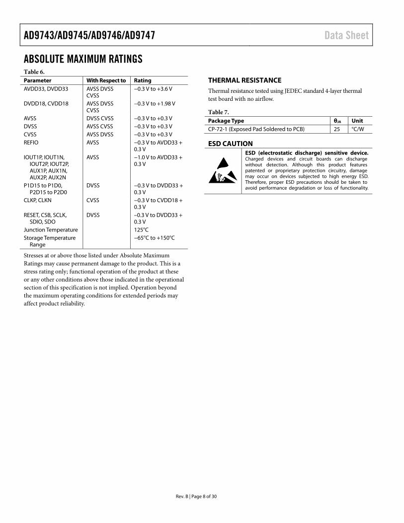
ABSOLUTE MAXIMUM RATINGS Table 6. Parameter With Respect to Rating AVDD33, DVDD33 AVSS DVSS
CVSS −0.3 V to +3.6 V
DVDD18, CVDD18 AVSS DVSS CVSS
−0.3 V to +1.98 V
AVSS DVSS CVSS −0.3 V to +0.3 V DVSS AVSS CVSS −0.3 V to +0.3 V CVSS AVSS DVSS −0.3 V to +0.3 V REFIO AVSS −0.3 V to AVDD33 +
0.3 V IOUT1P, IOUT1N,
IOUT2P, IOUT2P, AUX1P, AUX1N, AUX2P, AUX2N
AVSS −1.0 V to AVDD33 + 0.3 V
P1D15 to P1D0, P2D15 to P2D0
DVSS −0.3 V to DVDD33 + 0.3 V
CLKP, CLKN CVSS −0.3 V to CVDD18 + 0.3 V
RESET, CSB, SCLK, SDIO, SDO
DVSS –0.3 V to DVDD33 + 0.3 V
Junction Temperature 125°C Storage Temperature
Range −65°C to +150°C
Stresses at or above those listed under Absolute Maximum Ratings may cause permanent damage to the product. This is a stress rating only; functional operation of the product at these or any other conditions above those indicated in the operational section of this specification is not implied. Operation beyond the maximum operating conditions for extended periods may affect product reliability.
THERMAL RESISTANCE Thermal resistance tested using JEDEC standard 4-layer thermal test board with no airflow.
Table 7. Package Type θJA Unit CP-72-1 (Exposed Pad Soldered to PCB) 25 °C/W
ESD CAUTION
Data Sheet AD9743/AD9745/AD9746/AD9747
Rev. B | Page 9 of 30
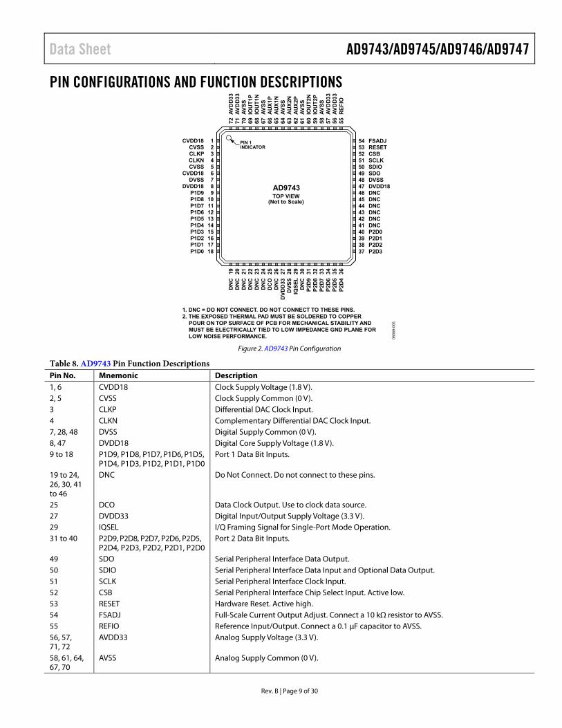
PIN CONFIGURATIONS AND FUNCTION DESCRIPTIONS
123456789
10111213141516
CVDD18CVSSCLKPCLKNCVSS
CVDD18DVSS
DVDD18P1D9P1D8P1D7P1D6P1D5P1D4P1D3P1D2
17P1D118P1D0
19 20 21 22 23 24 25 26 27 28 29 30 31 32 33 34
DN
CD
NC
DN
CD
NC
DN
CD
NC
DC
OD
NC
DVD
D33
DVS
SIQ
SEL
DN
CP2
D9
P2D
8P2
D7
P2D
635
P2D
536
P2D
4
545352515049484746454443424140393837
FSADJRESETCSBSCLKSDIOSDODVSSDVDD18DNCDNCDNCDNCDNCDNCP2D0P2D1P2D2P2D3
72 71 70 69 68 67 66 65 64 63 62 61 60 59 58 57 56 55
AVD
D33
AVD
D33
AVSS
IOU
T1P
IOU
T1N
AVSS
AU
X1P
AU
X1N
AVSS
AU
X2N
AU
X2P
AVSS
IOU
T2N
IOU
T2P
AVSS
AVD
D33
AVD
D33
REF
IO
0656
9-00
5
PIN 1INDICATOR
AD9743TOP VIEW
(Not to Scale)
1. DNC = DO NOT CONNECT. DO NOT CONNECT TO THESE PINS.2. THE EXPOSED THERMAL PAD MUST BE SOLDERED TO COPPER POUR ON TOP SURFACE OF PCB FOR MECHANICAL STABILITY AND MUST BE ELECTRICALLY TIED TO LOW IMPEDANCE GND PLANE FOR LOW NOISE PERFORMANCE.
Figure 2. AD9743 Pin Configuration
Table 8. AD9743 Pin Function Descriptions Pin No. Mnemonic Description 1, 6 CVDD18 Clock Supply Voltage (1.8 V). 2, 5 CVSS Clock Supply Common (0 V). 3 CLKP Differential DAC Clock Input. 4 CLKN Complementary Differential DAC Clock Input. 7, 28, 48 DVSS Digital Supply Common (0 V). 8, 47 DVDD18 Digital Core Supply Voltage (1.8 V). 9 to 18 P1D9, P1D8, P1D7, P1D6, P1D5,
P1D4, P1D3, P1D2, P1D1, P1D0 Port 1 Data Bit Inputs.
19 to 24, 26, 30, 41 to 46
DNC Do Not Connect. Do not connect to these pins.
25 DCO Data Clock Output. Use to clock data source. 27 DVDD33 Digital Input/Output Supply Voltage (3.3 V). 29 IQSEL I/Q Framing Signal for Single-Port Mode Operation. 31 to 40 P2D9, P2D8, P2D7, P2D6, P2D5,
P2D4, P2D3, P2D2, P2D1, P2D0 Port 2 Data Bit Inputs.
49 SDO Serial Peripheral Interface Data Output. 50 SDIO Serial Peripheral Interface Data Input and Optional Data Output. 51 SCLK Serial Peripheral Interface Clock Input. 52 CSB Serial Peripheral Interface Chip Select Input. Active low. 53 RESET Hardware Reset. Active high. 54 FSADJ Full-Scale Current Output Adjust. Connect a 10 kΩ resistor to AVSS. 55 REFIO Reference Input/Output. Connect a 0.1 μF capacitor to AVSS. 56, 57, 71, 72
AVDD33 Analog Supply Voltage (3.3 V).
58, 61, 64, 67, 70
AVSS Analog Supply Common (0 V).

AD9743/AD9745/AD9746/AD9747 Data Sheet
Rev. B | Page 10 of 30
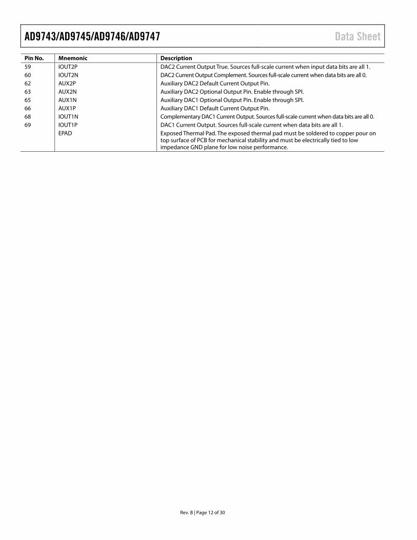
Pin No. Mnemonic Description 59 IOUT2P DAC2 Current Output True. Sources full-scale current when input data bits are all 1. 60 IOUT2N DAC2 Current Output Complement. Sources full-scale current when data bits are all 0. 62 AUX2P Auxiliary DAC2 Default Current Output Pin. 63 AUX2N Auxiliary DAC2 Optional Output Pin. Enable through SPI. 65 AUX1N Auxiliary DAC1 Optional Output Pin. Enable through SPI. 66 AUX1P Auxiliary DAC1 Default Current Output Pin. 68 IOUT1N Complementary DAC1 Current Output. Sources full-scale current when data bits are all 0. 69 IOUT1P DAC1 Current Output. Sources full-scale current when data bits are all 1. EPAD Exposed Thermal Pad. The exposed thermal pad must be soldered to copper pour on top
surface of PCB for mechanical stability and must be electrically tied to low impedance GND plane for low noise performance.
Data Sheet AD9743/AD9745/AD9746/AD9747
Rev. B | Page 11 of 30
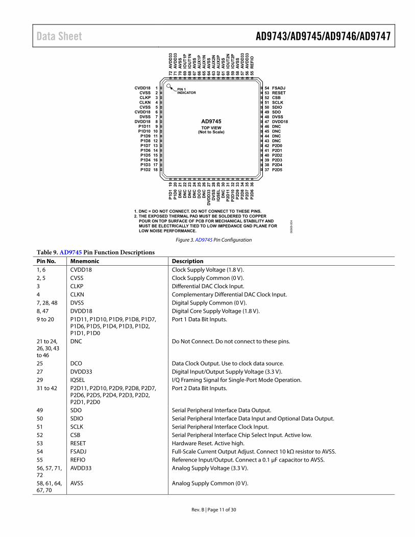
123456789
10111213141516
CVDD18CVSSCLKPCLKNCVSS
CVDD18DVSS
DVDD18P1D11P1D10P1D9P1D8P1D7P1D6P1D5P1D4
17P1D318P1D2
19 20 21 22 23 24 25 26 27 28 29 30 31 32 33 34
P1D
1P1
D0
DN
CD
NC
DN
CD
NC
DC
OD
NC
DVD
D33
DVS
SIQ
SEL
DN
CP2
D11
P2D
10P2
D9
P2D
835
P2D
736
P2D
6
545352515049484746454443424140393837
FSADJRESETCSBSCLKSDIOSDODVSSDVDD18DNCDNCDNCDNCP2D0P2D1P2D2P2D3P2D4P2D5
72 71 70 69 68 67 66 65 64 63 62 61 60 59 58 57 56 55
AVD
D33
AVD
D33
AVSS
IOU
T1P
IOU
T1N
AVSS
AU
X1P
AU
X1N
AVSS
AU
X2N
AU
X2P
AVSS
IOU
T2N
IOU
T2P
AVSS
AVD
D33
AVD
D33
REF
IO
0656
9-00
4
PIN 1INDICATOR
AD9745TOP VIEW
(Not to Scale)
1. DNC = DO NOT CONNECT. DO NOT CONNECT TO THESE PINS.2. THE EXPOSED THERMAL PAD MUST BE SOLDERED TO COPPER POUR ON TOP SURFACE OF PCB FOR MECHANICAL STABILITY AND MUST BE ELECTRICALLY TIED TO LOW IMPEDANCE GND PLANE FOR LOW NOISE PERFORMANCE.
Figure 3. AD9745 Pin Configuration
Table 9. AD9745 Pin Function Descriptions Pin No. Mnemonic Description 1, 6 CVDD18 Clock Supply Voltage (1.8 V). 2, 5 CVSS Clock Supply Common (0 V). 3 CLKP Differential DAC Clock Input. 4 CLKN Complementary Differential DAC Clock Input. 7, 28, 48 DVSS Digital Supply Common (0 V). 8, 47 DVDD18 Digital Core Supply Voltage (1.8 V). 9 to 20 P1D11, P1D10, P1D9, P1D8, P1D7,
P1D6, P1D5, P1D4, P1D3, P1D2, P1D1, P1D0
Port 1 Data Bit Inputs.
21 to 24, 26, 30, 43 to 46
DNC Do Not Connect. Do not connect to these pins.
25 DCO Data Clock Output. Use to clock data source. 27 DVDD33 Digital Input/Output Supply Voltage (3.3 V). 29 IQSEL I/Q Framing Signal for Single-Port Mode Operation. 31 to 42 P2D11, P2D10, P2D9, P2D8, P2D7,
P2D6, P2D5, P2D4, P2D3, P2D2, P2D1, P2D0
Port 2 Data Bit Inputs.
49 SDO Serial Peripheral Interface Data Output. 50 SDIO Serial Peripheral Interface Data Input and Optional Data Output. 51 SCLK Serial Peripheral Interface Clock Input. 52 CSB Serial Peripheral Interface Chip Select Input. Active low. 53 RESET Hardware Reset. Active high. 54 FSADJ Full-Scale Current Output Adjust. Connect 10 kΩ resistor to AVSS. 55 REFIO Reference Input/Output. Connect a 0.1 μF capacitor to AVSS. 56, 57, 71, 72
AVDD33 Analog Supply Voltage (3.3 V).
58, 61, 64, 67, 70
AVSS Analog Supply Common (0 V).
AD9743/AD9745/AD9746/AD9747 Data Sheet
Rev. B | Page 12 of 30
Pin No. Mnemonic Description 59 IOUT2P DAC2 Current Output True. Sources full-scale current when input data bits are all 1. 60 IOUT2N DAC2 Current Output Complement. Sources full-scale current when data bits are all 0. 62 AUX2P Auxiliary DAC2 Default Current Output Pin. 63 AUX2N Auxiliary DAC2 Optional Output Pin. Enable through SPI. 65 AUX1N Auxiliary DAC1 Optional Output Pin. Enable through SPI. 66 AUX1P Auxiliary DAC1 Default Current Output Pin. 68 IOUT1N Complementary DAC1 Current Output. Sources full-scale current when data bits are all 0. 69 IOUT1P DAC1 Current Output. Sources full-scale current when data bits are all 1. EPAD Exposed Thermal Pad. The exposed thermal pad must be soldered to copper pour on
top surface of PCB for mechanical stability and must be electrically tied to low impedance GND plane for low noise performance.
Data Sheet AD9743/AD9745/AD9746/AD9747
Rev. B | Page 13 of 30
123456789
10111213141516
CVDD18CVSSCLKPCLKNCVSS
CVDD18DVSS
DVDD18P1D13P1D12P1D11P1D10
P1D9P1D8P1D7P1D6
17P1D518P1D4
19 20 21 22 23 24 25 26 27 28 29 30 31 32 33 34
P1D
3P1
D2
P1D
1P1
D0
DN
CD
NC
DC
OD
NC
DVD
D33
DVS
SIQ
SEL
DN
CP2
D13
P2D
12P2
D11
P2D
1035
P2D
936
P2D
8
545352515049484746454443424140393837
FSADJRESETCSBSCLKSDIOSDODVSSDVDD18DNCDNCP2D0P2D1P2D2P2D3P2D4P2D5P2D6P2D7
72 71 70 69 68 67 66 65 64 63 62 61 60 59 58 57 56 55
AVD
D33
A VD
D33
AVSS
IOU
T1P
IOU
T1N
AVSS
AU
X1P
AU
X1N
AVSS
AU
X2N
AU
X2P
AVSS
IOU
T2N
IOU
T2P
AVSS
AVD
D33
AVD
D33
REF
IO
0656
9-00
3
PIN 1INDICATOR
AD9746
1. DNC = DO NOT CONNECT. DO NOT CONNECT TO THESE PINS.2. THE EXPOSED THERMAL PAD MUST BE SOLDERED TO COPPER POUR ON TOP SURFACE OF PCB FOR MECHANICAL STABILITY AND MUST BE ELECTRICALLY TIED TO LOW IMPEDANCE GND PLANE FOR LOW NOISE PERFORMANCE.
TOP VIEW(Not to Scale)
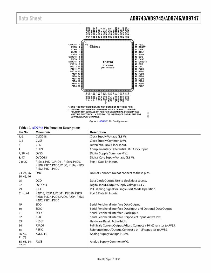
Figure 4. AD9746 Pin Configuration
Table 10. AD9746 Pin Function Descriptions Pin No. Mnemonic Description 1, 6 CVDD18 Clock Supply Voltage (1.8 V). 2, 5 CVSS Clock Supply Common (0 V). 3 CLKP Differential DAC Clock Input. 4 CLKN Complementary Differential DAC Clock Input. 7, 28, 48 DVSS Digital Supply Common (0 V). 8, 47 DVDD18 Digital Core Supply Voltage (1.8 V). 9 to 22 P1D13, P1D12, P1D11, P1D10, P1D9,
P1D8, P1D7, P1D6, P1D5, P1D4, P1D3, P1D2, P1D1, P1D0
Port 1 Data Bit Inputs.
23, 24, 26, 30, 45, 46
DNC Do Not Connect. Do not connect to these pins.
25 DCO Data Clock Output. Use to clock data source. 27 DVDD33 Digital Input/Output Supply Voltage (3.3 V). 29 IQSEL I/Q Framing Signal for Single-Port Mode Operation. 31 to 44 P2D13, P2D12, P2D11, P2D10, P2D9,
P2D8, P2D7, P2D6, P2D5, P2D4, P2D3, P2D2, P2D1, P2D0
Port 2 Data Bit Inputs.
49 SDO Serial Peripheral Interface Data Output. 50 SDIO Serial Peripheral Interface Data Input and Optional Data Output. 51 SCLK Serial Peripheral Interface Clock Input. 52 CSB Serial Peripheral Interface Chip Select Input. Active low. 53 RESET Hardware Reset. Active high. 54 FSADJ Full-Scale Current Output Adjust. Connect a 10 kΩ resistor to AVSS. 55 REFIO Reference Input/Output. Connect a 0.1 μF capacitor to AVSS. 56, 57, 71, 72
AVDD33 Analog Supply Voltage (3.3 V).
58, 61, 64, 67, 70
AVSS Analog Supply Common (0 V).
AD9743/AD9745/AD9746/AD9747 Data Sheet
Rev. B | Page 14 of 30
Pin No. Mnemonic Description 59 IOUT2P DAC2 Current Output True. Sources full-scale current when input data bits are all 1. 60 IOUT2N DAC2 Current Output Complement. Sources full-scale current when data bits are all 0. 62 AUX2P Auxiliary DAC2 Default Current Output Pin. 63 AUX2N Auxiliary DAC2 Optional Output Pin. Enable through SPI. 65 AUX1N Auxiliary DAC1 Optional Output Pin. Enable through SPI. 66 AUX1P Auxiliary DAC1 Default Current Output Pin. 68 IOUT1N Complementary DAC1 Current Output. Sources full-scale current when data bits are all 0. 69 IOUT1P DAC1 Current Output. Sources full-scale current when data bits are all 1. EPAD Exposed Thermal Pad. The exposed thermal pad must be soldered to copper pour
on top surface of PCB for mechanical stability and must be electrically tied to low impedance GND plane for low noise performance.

Data Sheet AD9743/AD9745/AD9746/AD9747
Rev. B | Page 15 of 30
123456789
10111213141516
CVDD18CVSSCLKPCLKNCVSS
CVDD18DVSS
DVDD18P1D15P1D14P1D13P1D12P1D11P1D10
P1D9P1D8
17P1D718P1D6
19 20 21 22 23 24 25 26 27 28 29 30 31 32 33 34
P1D
5P1
D4
P1D
3P1
D2
P1D
1P1
D0
DC
OD
NC
DVD
D33
DVS
SIQ
SEL
DN
CP2
D15
P2D
14P2
D13
P2D
1235
P2D
1136
P2D
10
545352515049484746454443424140393837
FSADJRESETCSBSCLKSDIOSDODVSSDVDD18P2D0P2D1P2D2P2D3P2D4P2D5P2D6P2D7P2D8P2D9
72 71 70 69 68 67 66 65 64 63 62 61 60 59 58 57 56 55
AVD
D33
AVD
D33
AVSS
IOU
T1P
IOU
T1N
AVSS
AU
X1P
AU
X1N
AVSS
AU
X2N
AU
X2P
AVSS
IOU
T2N
IOU
T2P
AVSS
AVD
D33
AVD
D33
REF
IO
1. DNC = DO NOT CONNECT. DO NOT CONNECT TO THESE PINS.2. THE EXPOSED THERMAL PAD MUST BE SOLDERED TO COPPER POUR ON TOP SURFACE OF PCB FOR MECHANICAL STABILITY AND MUST BE ELECTRICALLY TIED TO LOW IMPEDANCE GND PLANE FOR LOW NOISE PERFORMANCE. 06
569-
002
PIN 1INDICATOR
AD9747TOP VIEW
(Not to Scale)
Figure 5. AD9747 Pin Configuration
Table 11. AD9747 Pin Function Descriptions Pin No. Mnemonic Description 1, 6 CVDD18 Clock Supply Voltage (1.8 V). 2, 5 CVSS Clock Supply Common (0 V). 3 CLKP Differential DAC Clock Input. 4 CLKN Complementary Differential DAC Clock Input. 7, 28, 48 DVSS Digital Supply Common (0 V). 8, 47 DVDD18 Digital Core Supply Voltage (1.8 V). 9 to 24 P1D15, P1D14, P1D13, P1D12, P1D11,
P1D10, P1D9, P1D8, P1D7, P1D6, P1D5, P1D4, P1D3, P1D2, P1D1, P1D0
Port 1 Data Bit Inputs.
25 DCO Data Clock Output. Use to clock data source. 26, 30 DNC Do Not Connect. Do not connect to these pins. 27 DVDD33 Digital Input/Output Supply Voltage (3.3 V). 29 IQSEL I/Q Framing Signal for Single-Port Mode Operation. 31 to 46 P2D15, P2D14, P2D13, P2D12, P2D11,
P2D10, P2D9, P2D8, P2D7, P2D6, P2D5, P2D4, P2D3, P2D2, P2D1, P2D0
Port 2 Data Bit Inputs.
49 SDO Serial Peripheral Interface Data Output. 50 SDIO Serial Peripheral Interface Data Input and Optional Data Output. 51 SCLK Serial Peripheral Interface Clock Input. 52 CSB Serial Peripheral Interface Chip Select Input. Active low. 53 RESET Hardware Reset. Active high. 54 FSADJ Full-Scale Current Output Adjust. Connect a 10 kΩ resistor to AVSS. 55 REFIO Reference Input/Output. Connect a 0.1 μF capacitor to AVSS. 56, 57, 71, 72
AVDD33 Analog Supply Voltage (3.3 V).
58, 61, 64, 67, 70
AVSS Analog Supply Common (0 V).

AD9743/AD9745/AD9746/AD9747 Data Sheet
Rev. B | Page 16 of 30
Pin No. Mnemonic Description 59 IOUT2P DAC2 Current Output. Sources full-scale current when input data bits are all 1. 60 IOUT2N Complementary DAC2 Current Output. Sources full-scale current when data bits are all 0. 62 AUX2P Auxiliary DAC2 Default Current Output Pin. 63 AUX2N Auxiliary DAC2 Optional Output Pin. Enable through SPI. 65 AUX1N Auxiliary DAC1 Optional Output Pin. Enable through SPI. 66 AUX1P Auxiliary DAC1 Default Current Output Pin. 68 IOUT1N Complementary DAC1 Current Output. Sources full-scale current when data bits are all 0. 69 IOUT1P DAC1 Current Output. Sources full-scale current when data bits are all 1. EPAD Exposed Thermal Pad. The exposed thermal pad must be soldered to copper pour on
top surface of PCB for mechanical stability and must be electrically tied to low impedance GND plane for low noise performance.
Data Sheet AD9743/AD9745/AD9746/AD9747
Rev. B | Page 17 of 30
TYPICAL PERFORMANCE CHARACTERISTICS
40
50
60
70
80
90
100
0 20 40 60 80 100 120
250MSPS
125MSPS
0656
9-00
7
fOUT (MHz)
SFD
R (d
Bc)
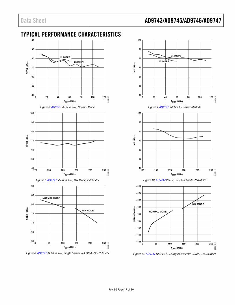
Figure 6. AD9747 SFDR vs. fOUT, Normal Mode
150 175 200 22540
50
60
70
80
90
100
125 250
0656
9-00
8
fOUT (MHz)
SFD
R (d
Bc)
Figure 7. AD9747 SFDR vs. fOUT, Mix Mode, 250 MSPS
60
65
70
75
80
85
90
50 100 150 2000 250
0656
9-00
9
fOUT (MHz)
AC
LR (d
Bc)
NORMAL MODE
MIX MODE
Figure 8. AD9747 ACLR vs. fOUT, Single Carrier W-CDMA, 245.76 MSPS
40
50
60
70
80
90
100
0 20 40 60 80 100 120
250MSPS
0656
9-01
0
fOUT (MHz)
IMD
(dB
c)
125MSPS
Figure 9. AD9747 IMD vs. fOUT, Normal Mode
150 175 200 22540
50
60
70
80
90
100
125 250
0656
9-01
1
fOUT (MHz)
IMD
(dB
c)
Figure 10. AD9747 IMD vs. fOUT, Mix Mode, 250 MSPS
–168
–166
–164
–162
–160
–158
–156
–154
–152
50 100 150 2000 250
0656
9-01
2
fOUT (MHz)
NSD
(dB
m/H
z)
NORMAL MODE
MIX MODE
Figure 11. AD9747 NSD vs. fOUT, Single Carrier W-CDMA, 245.76 MSPS
AD9743/AD9745/AD9746/AD9747 Data Sheet
Rev. B | Page 18 of 30
30mAFS
40
50
60
70
80
90
100
0 20 40 60 80 100 120
0656
9-03
6
fOUT (MHz)
SFD
R (d
Bc)
10mAFS
20mAFS
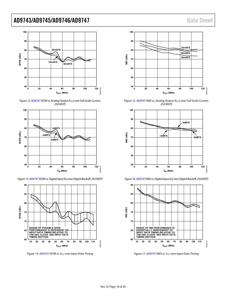
Figure 12. AD9747 SFDR vs. Analog Output (fOUT) over Full-Scale Current, 250 MSPS
–3dBFS
40
50
60
70
80
90
100
0 20 40 60 80 100 120
0656
9-03
7
fIN (MHz)
SFD
R (d
Bc)
–6dBFS
0dBFS
Figure 13. AD9747 SFDR vs. Digital Input (fIN) over Digital Backoff, 250 MSPS
60
65
70
75
80
85
90
10 20 30 40 50 60 70 80 90 100 110
RANGE OF POSSIBLE SFDRPERFORMANCE IS DEPENDENT ONINPUT DATA TIMING RELATIVE TOTHE DAC CLOCK. SEE INPUT DATATIMING SECTION.
0656
9-03
8
fOUT (MHz)
SFD
R (d
Bc)
Figure 14. AD9747 SFDR vs. fOUT over Input Data Timing
10mAFS
20mAFS
30mAFS
40
50
60
70
80
90
100
0 20 40 60 80 100 120
0656
9-03
9
fOUT (MHz)
IMD
(dB
c)
Figure 15. AD9747 IMD vs. Analog Output (fOUT) over Full-Scale Current, 250 MSPS
0dBFS
–3dBFS
40
50
60
70
80
90
100
0 20 40 60 80 100 120
0656
9-04
0
fIN (MHz)
IMD
(dB
c)
–6dBFS
Figure 16. AD9747 IMD vs. Digital Input (fIN) over Digital Backoff, 250 MSPS
fOUT (MHz)
60
65
70
75
80
85
90
20 30 40 50 60 70 80 90 100 11010
0656
9-04
1
IMD
(dB
c)
RANGE OF IMD PERFORMANCE ISESSENTIALLY INDEPENDENT OFINPUT DATA TIMING RELATIVE TOTHE DAC CLOCK. SEE INPUT DATATIMING SECTION.
Figure 17. AD9747 IMD vs. fOUT over Input Data Timing
Data Sheet AD9743/AD9745/AD9746/AD9747
Rev. B | Page 19 of 30
–5
–4
–3
–2
–1
0
1
25 75 125 175 22550 100 150 2000 250
0656
9-04
2
fOUT (MHz)
AO
UT
(dB
m)
NORMAL MODE
MIX MODE
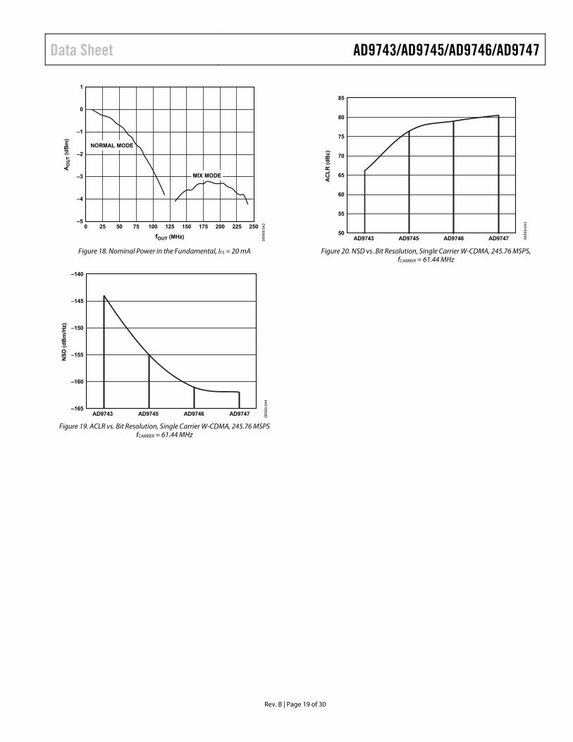
Figure 18. Nominal Power in the Fundamental, IFS = 20 mA
–165
–160
–155
–150
–145
–140
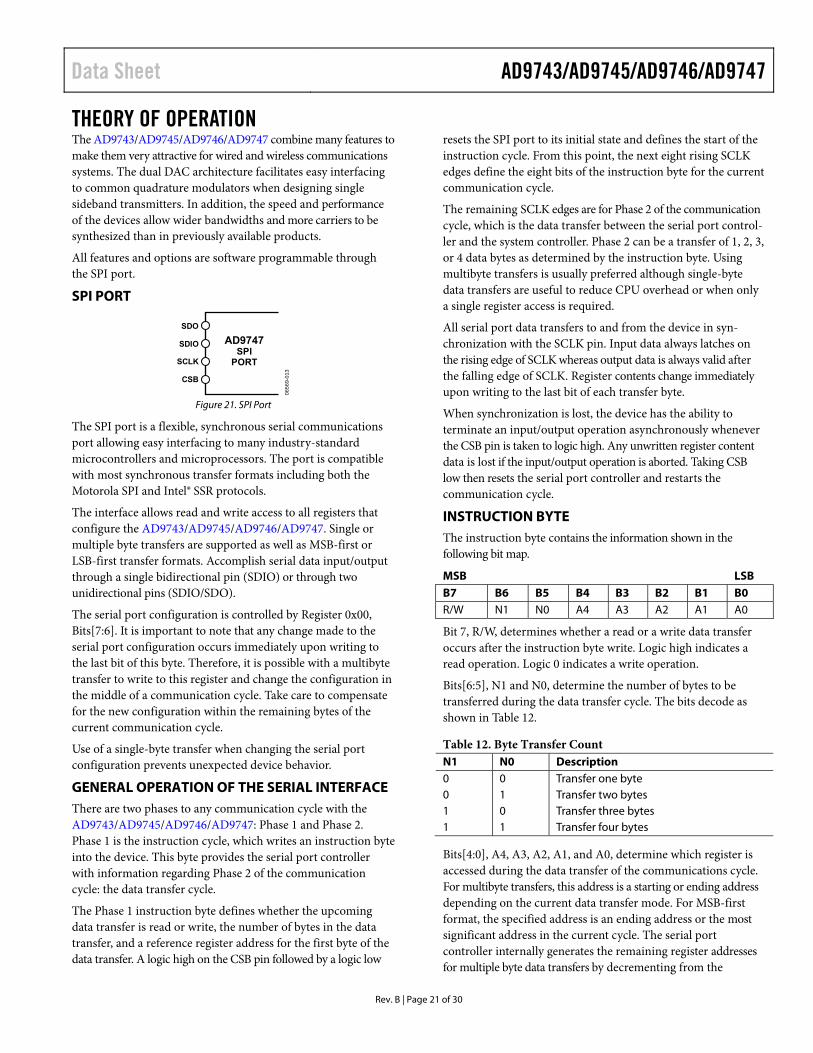
AD9747AD9746AD9745AD9743 0656
9-04
4
NSD
(dB
m/H
z)
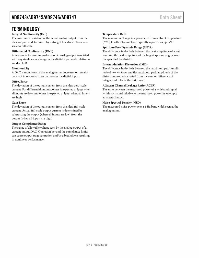
Figure 19. ACLR vs. Bit Resolution, Single Carrier W-CDMA, 245.76 MSPS
fCARRIER = 61.44 MHz
50
55
60
65
70
75
80
85
AD9747AD9746AD9745AD9743 0656
9-04
3
AC
LR (d
Bc)
Figure 20. NSD vs. Bit Resolution, Single Carrier W-CDMA, 245.76 MSPS,
fCARRIER = 61.44 MHz
AD9743/AD9745/AD9746/AD9747 Data Sheet
Rev. B | Page 20 of 30
TERMINOLOGY Integral Nonlinearity (INL) The maximum deviation of the actual analog output from the ideal output, as determined by a straight line drawn from zero scale to full scale.
Differential Nonlinearity (DNL) A measure of the maximum deviation in analog output associated with any single value change in the digital input code relative to an ideal LSB.
Monotonicity A DAC is monotonic if the analog output increases or remains constant in response to an increase in the digital input.
Offset Error The deviation of the output current from the ideal zero-scale current. For differential outputs, 0 mA is expected at IOUTP when all inputs are low, and 0 mA is expected at IOUTN when all inputs are high.
Gain Error The deviation of the output current from the ideal full-scale current. Actual full-scale output current is determined by subtracting the output (when all inputs are low) from the output (when all inputs are high).
Output Compliance Range The range of allowable voltage seen by the analog output of a current output DAC. Operation beyond the compliance limits can cause output stage saturation and/or a breakdown resulting in nonlinear performance.
Temperature Drift The maximum change in a parameter from ambient temperature (25°C) to either TMIN or TMAX, typically reported as ppm/°C.
Spurious-Free Dynamic Range (SFDR) The difference in decibels between the peak amplitude of a test tone and the peak amplitude of the largest spurious signal over the specified bandwidth.
Intermodulation Distortion (IMD) The difference in decibels between the maximum peak ampli-tude of two test tones and the maximum peak amplitude of the distortion products created from the sum or difference of integer multiples of the test tones.
Adjacent Channel Leakage Ratio (ACLR) The ratio between the measured power of a wideband signal within a channel relative to the measured power in an empty adjacent channel.
Noise Spectral Density (NSD) The measured noise power over a 1 Hz bandwidth seen at the analog output.
Data Sheet AD9743/AD9745/AD9746/AD9747
Rev. B | Page 21 of 30
THEORY OF OPERATION The AD9743/AD9745/AD9746/AD9747 combine many features to make them very attractive for wired and wireless communications systems. The dual DAC architecture facilitates easy interfacing to common quadrature modulators when designing single sideband transmitters. In addition, the speed and performance of the devices allow wider bandwidths and more carriers to be synthesized than in previously available products.
All features and options are software programmable through the SPI port.
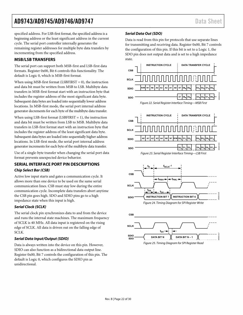
SPI PORT
AD9747SPI
PORT
SDO
SDIO
SCLK
CSB
065
69-
01
3
Figure 21. SPI Port
The SPI port is a flexible, synchronous serial communications port allowing easy interfacing to many industry-standard microcontrollers and microprocessors. The port is compatible with most synchronous transfer formats including both the Motorola SPI and Intel® SSR protocols.
The interface allows read and write access to all registers that configure the AD9743/AD9745/AD9746/AD9747. Single or multiple byte transfers are supported as well as MSB-first or LSB-first transfer formats. Accomplish serial data input/output through a single bidirectional pin (SDIO) or through two unidirectional pins (SDIO/SDO).
The serial port configuration is controlled by Register 0x00, Bits[7:6]. It is important to note that any change made to the serial port configuration occurs immediately upon writing to the last bit of this byte. Therefore, it is possible with a multibyte transfer to write to this register and change the configuration in the middle of a communication cycle. Take care to compensate for the new configuration within the remaining bytes of the current communication cycle.
Use of a single-byte transfer when changing the serial port configuration prevents unexpected device behavior.
GENERAL OPERATION OF THE SERIAL INTERFACE There are two phases to any communication cycle with the AD9743/AD9745/AD9746/AD9747: Phase 1 and Phase 2. Phase 1 is the instruction cycle, which writes an instruction byte into the device. This byte provides the serial port controller with information regarding Phase 2 of the communication cycle: the data transfer cycle.
The Phase 1 instruction byte defines whether the upcoming data transfer is read or write, the number of bytes in the data transfer, and a reference register address for the first byte of the data transfer. A logic high on the CSB pin followed by a logic low
resets the SPI port to its initial state and defines the start of the instruction cycle. From this point, the next eight rising SCLK edges define the eight bits of the instruction byte for the current communication cycle.
The remaining SCLK edges are for Phase 2 of the communication cycle, which is the data transfer between the serial port control-ler and the system controller. Phase 2 can be a transfer of 1, 2, 3, or 4 data bytes as determined by the instruction byte. Using multibyte transfers is usually preferred although single-byte data transfers are useful to reduce CPU overhead or when only a single register access is required.
All serial port data transfers to and from the device in syn-chronization with the SCLK pin. Input data always latches on the rising edge of SCLK whereas output data is always valid after the falling edge of SCLK. Register contents change immediately upon writing to the last bit of each transfer byte.
When synchronization is lost, the device has the ability to terminate an input/output operation asynchronously whenever the CSB pin is taken to logic high. Any unwritten register content data is lost if the input/output operation is aborted. Taking CSB low then resets the serial port controller and restarts the communication cycle.
INSTRUCTION BYTE The instruction byte contains the information shown in the following bit map.
MSB LSB B7 B6 B5 B4 B3 B2 B1 B0 R/W N1 N0 A4 A3 A2 A1 A0
Bit 7, R/W, determines whether a read or a write data transfer occurs after the instruction byte write. Logic high indicates a read operation. Logic 0 indicates a write operation.
Bits[6:5], N1 and N0, determine the number of bytes to be transferred during the data transfer cycle. The bits decode as shown in Table 12.
Table 12. Byte Transfer Count N1 N0 Description 0 0 Transfer one byte 0 1 Transfer two bytes 1 0 Transfer three bytes 1 1 Transfer four bytes
Bits[4:0], A4, A3, A2, A1, and A0, determine which register is accessed during the data transfer of the communications cycle. For multibyte transfers, this address is a starting or ending address depending on the current data transfer mode. For MSB-first format, the specified address is an ending address or the most significant address in the current cycle. The serial port controller internally generates the remaining register addresses for multiple byte data transfers by decrementing from the
AD9743/AD9745/AD9746/AD9747 Data Sheet
Rev. B | Page 22 of 30
specified address. For LSB-first format, the specified address is a beginning address or the least significant address in the current cycle. The serial port controller internally generates the remaining register addresses for multiple byte data transfers by incrementing from the specified address.
MSB/LSB TRANSFERS The serial port can support both MSB-first and LSB-first data formats. Register 0x00, Bit 6 controls this functionality. The default is Logic 0, which is MSB-first format.
When using MSB-first format (LSBFIRST = 0), the instruction and data bit must be written from MSB to LSB. Multibyte data transfers in MSB-first format start with an instruction byte that includes the register address of the most significant data byte. Subsequent data bytes are loaded into sequentially lower address locations. In MSB-first mode, the serial port internal address generator decrements for each byte of the multibyte data transfer.
When using LSB-first format (LSBFIRST = 1), the instruction and data bit must be written from LSB to MSB. Multibyte data transfers in LSB-first format start with an instruction byte that includes the register address of the least significant data byte. Subsequent data bytes are loaded into sequentially higher address locations. In LSB-first mode, the serial port internal address generator increments for each byte of the multibyte data transfer.
Use of a single-byte transfer when changing the serial port data format prevents unexpected device behavior.
SERIAL INTERFACE PORT PIN DESCRIPTIONS Chip Select Bar (CSB)
Active low input starts and gates a communication cycle. It allows more than one device to be used on the same serial communication lines. CSB must stay low during the entire communication cycle. Incomplete data transfers abort anytime the CSB pin goes high. SDO and SDIO pins go to a high impedance state when this input is high.
Serial Clock (SCLK)
The serial clock pin synchronizes data to and from the device and runs the internal state machines. The maximum frequency of SCLK is 40 MHz. All data input is registered on the rising edge of SCLK. All data is driven out on the falling edge of SCLK.
Serial Data Input/Output (SDIO)
Data is always written into the device on this pin. However, SDIO can also function as a bidirectional data output line. Register 0x00, Bit 7 controls the configuration of this pin. The default is Logic 0, which configures the SDIO pin as unidirectional.
Serial Data Out (SDO)
Data is read from this pin for protocols that use separate lines for transmitting and receiving data. Register 0x00, Bit 7 controls the configuration of this pin. If this bit is set to a Logic 1, the SDO pin does not output data and is set to a high impedance state.
R/W N1 N0 A4 A3 A2 A1 A0 D7 D6N D5N D00D10D20D30
D7 D6N D5N D00D10D20D30
INSTRUCTION CYCLE DATA TRANSFER CYCLE
CSB
SCLK
SDIO
SDO
06
569-
014
Figure 22. Serial Register Interface Timing—MSB First
A0 A1 A2 A3 A4 N0 N1 R/W D00 D10 D20 D7ND6ND5ND4N
D00 D10 D20 D7ND6ND5ND4N
INSTRUCTION CYCLE DATA TRANSFER CYCLE
CSB
SCLK
SDIO
SDO
06
56
9-0
15
Figure 23. Serial Register Interface Timing—LSB First
INSTRUCTION BIT 6INSTRUCTION BIT 7
CSB
SCLK
SDIO
tS
tDS tDH
tPWH tPWL
fSCLK–1
065
69-
016
Figure 24. Timing Diagram for SPI Register Write
DATA BIT N – 1DATA BIT N
CSB
SCLK
SDIOSDO
tDV
0656
9-01
7
Figure 25. Timing Diagram for SPI Register Read
Data Sheet AD9743/AD9745/AD9746/AD9747
Rev. B | Page 23 of 30
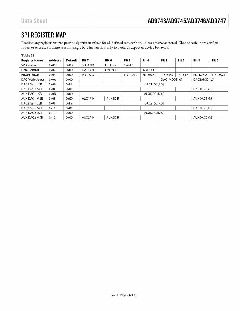
SPI REGISTER MAP Reading any register returns previously written values for all defined register bits, unless otherwise noted. Change serial port configu-ration or execute software reset in single byte instruction only to avoid unexpected device behavior.
Table 13. Register Name Address Default Bit 7 Bit 6 Bit 5 Bit 4 Bit 3 Bit 2 Bit 1 Bit 0 SPI Control 0x00 0x00 SDIODIR LSBFIRST SWRESET
Data Control 0x02 0x00 DATTYPE ONEPORT INVDCO Power Down 0x03 0x00 PD_DCO PD_AUX2 PD_AUX1 PD_BIAS PC_CLK PD_DAC2 PD_DAC1
DAC Mode Select 0x0A 0x00 DAC1MOD[1:0] DAC2MOD[1:0]
DAC1 Gain LSB 0x0B 0xF9 DAC1FSC[7:0]
DAC1 Gain MSB 0x0C 0x01 DAC1FSC[9:8]
AUX DAC1 LSB 0x0D 0x00 AUXDAC1[7:0]
AUX DAC1 MSB 0x0E 0x00 AUX1PIN AUX1DIR AUXDAC1[9:8]
DAC2 Gain LSB 0x0F 0xF9 DAC2FSC[7:0]
DAC2 Gain MSB 0x10 0x01 DAC2FSC[9:8]
AUX DAC2 LSB 0x11 0x00 AUXDAC2[7:0]
AUX DAC2 MSB 0x12 0x00 AUX2PIN AUX2DIR AUXDAC2[9:8]

AD9743/AD9745/AD9746/AD9747 Data Sheet
Rev. B | Page 24 of 30
SPI REGISTER DESCRIPTIONS Table 14. Register Address Bit Name Description SPI Control 0x00 7 SDIODIR 0 = operate SPI in 4-wire mode, SDIO pin operates as an input only 1 = operate SPI in 3-wire mode, SDIO pin operates as a bidirectional input/output line 6 LSBFIRST 0 = LSBFIRST off, SPI serial data mode is MSB to LSB 1 = LSBFIRST on, SPI serial data mode is LSB to MSB 5 SWRESET 0 = resume normal operation following software RESET 1 = software RESET; loads default values to all registers (except Register 0x00) Data Control 0x02 7 DATTYPE 0 = DAC input data is twos complement binary format 1 = DAC input data is unsigned binary format 6 ONEPORT 0 = normal dual-port input mode 1 = optional single port input mode, interleaved data received on Port 1 only 4 INVDCO 1 = inverts data clock output signal Power Down 0x03 7 PD_DCO 1 = power down data clock output 5 PD_AUX2 1 = power down AUX2 DAC 4 PD_AUX1 1 = power down AUX1 DAC 3 PD_BIAS 1 = power down reference voltage bias circuit 2 PD_CLK 1 = power down DAC clock input circuit 1 PD_DAC2 1 = power down DAC2 analog output 0 PD_DAC1 1 = power down DAC1 analog output DAC Mode Select 0x0A 3:2 DAC1MOD[1:0] 00 = selects normal mode, DAC1 01 = selects mix mode, DAC1 10 = selects return to zero mode, DAC1 1:0 DAC2MOD[1:0] 00 = selects normal mode, DAC2 01 = selects mix mode, DAC2 10 = selects return to zero mode, DAC2 DAC1 Gain 0x0B 7:0 DAC1FSC[7:0] DAC1 full-scale 10-bit adjustment word 0x0C 1:0 DAC1FSC[9:8] 0x03FF = sets full-scale current to the maximum value of 31.66 mA 0x01F9 = sets full-scale current to the nominal value of 20.0 mA 0x0000 = sets full-scale current to the minimum value of 8.64 mA AUX DAC1 0x0D 7:0 AUXDAC1[7:0] Auxiliary DAC1 10-bit output current adjustment word 0x0E 1:0 AUXDAC1[9:8] 0x03FF = sets output current magnitude to 2.0 mA 0x0200 = sets output current magnitude to 1.0 mA 0x0000 = sets output current magnitude to 0.0 mA 7 AUX1PIN 1 = AUX1P output pin is active 0 = AUX1N output pin is active 6 AUX1DIR 0 = configures AUX1 DAC output to source current 1 = configures AUX1 DAC output to sink current DAC2 Gain 0x0F 7:0 DAC2FSC[7:0] DAC2 full-scale 10-bit adjustment word 0x10 1:0 DAC2FSC[9:8] 0x03FF = sets full-scale current to the maximum value of 31.66 mA 0x01F9 = sets full-scale current to the nominal value of 20.0 mA 0x0000 = sets full-scale current to the minimum value of 8.64 mA AUX DAC2 0x11 7:0 AUXDAC2[7:0] Auxiliary DAC2 10-bit output current adjustment word 0x12 1:0 AUXDAC2[9:8] 0x03FF = sets output current magnitude to 2.0 mA 0x0200 = sets output current to 1.0 mA 0x0000 = sets output current to 0.0 mA 7 AUX2PIN 1 = AUX2P output pin is active 0 = AUX2N output pin is active 6 AUX2DIR 0 = configures AUX2 DAC output to source current 1 = configures AUX2 DAC output to sink current
Data Sheet AD9743/AD9745/AD9746/AD9747
Rev. B | Page 25 of 30
DIGITAL INPUTS AND OUTPUTS The AD9743/AD9745/AD9746/AD9747 can operate in two data input modes: dual-port mode and single-port mode. For the default dual-port mode (ONEPORT = 0), each DAC receives data from a dedicated input port. In single-port mode (ONEPORT = 1), however, both DACs receive data from Port 1. In single-port mode, DAC1 and DAC2 data is interleaved and the IQSEL input steers data to the correct DAC.
In single-port mode, when the IQSEL input is high, Port 1 data is delivered to DAC1 and when IQSEL is low, Port 1 data is delivered to DAC2. The IQSEL input must always coincide and be time-aligned with the other data bus signals. In single-port mode, minimum setup and hold times apply to the IQSEL input as well as to the input data signals. In dual-port mode, the IQSEL input is ignored.
In dual-port mode, the data must be delivered at the sample rate (up to 250 MSPS). In single-port mode, data must be delivered at twice the sample rate. Because the data inputs function only up to 250 MSPS, it is only practical to operate the DAC clock at up to 125 MHz in single-port mode.
In both dual-port and single-port modes, a data clock output (DCO) signal is available as a fixed time base with which to stimulate data from an FPGA. This output signal always operates at the sample rate. It can be inverted by asserting the INVDCO bit.
INPUT DATA TIMING With most DACs, signal-to-noise ratio (SNR) is a function of the relationship between the position of the clock edges and the point in time at which the input data changes. The AD9743/ AD9745/AD9746/AD9747 are rising edge triggered and thus exhibit greater SNR sensitivity when the data transition is close to this edge.
The specified minimum setup and hold times define a window of time, within each data period, where the data is sampled correctly. Users must position data to arrive relative to the DAC clock and well beyond the minimum setup and minimum hold times. This becomes increasingly more important at increasingly higher sample rates.
DUAL-PORT MODE TIMING Figure 26 shows the timing diagram for the dual-port mode. CLKP/CLKN
DCO
P1D<15:0>
P2D<15:0>
tDCO
tDBHtDBS
06
569
-01
8
I1 I2 I3 I4
Q1 Q2 Q3 Q4
Figure 26. Data Interface Timing, Dual-Port Mode
In Figure 26, data samples for DAC1 are labeled Ix and data samples for DAC2 are labeled Qx. Note that the differential DAC clock input is shown in a logical sense (CLKP/CLKN). The data clock output is labeled DCO.
Setup and hold times are referenced to the positive transition of the DAC clock. Data must arrive at the input pins such that the minimum setup and hold times are met. Note that the data clock output has a fixed time delay from the DAC clock and may be a more convenient signal to use to confirm timing.
SINGLE-PORT MODE TIMING Figure 27 shows the single-port mode timing diagram.
065
69-
01
9
CLKP/CLKN
DCO
P1D<15:0>
IQSEL
tDBStDBH
tDCO
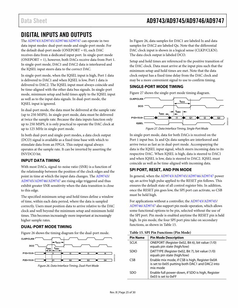
I1 Q1 I2 Q2
Figure 27. Data Interface Timing, Single-Port Mode
In single-port mode, data for both DACs is received on the Port 1 input bus. Ix and Qx data samples are interleaved and arrive twice as fast as in dual-port mode. Accompanying the data is the IQSEL input signal, which steers incoming data to its respective DAC. When IQSEL is high, data is steered to DAC1 and when IQSEL is low, data is steered to DAC2. IQSEL must coincide as well as be time-aligned with incoming data.
SPI PORT, RESET, AND PIN MODE In general, when the AD9743/AD9745/AD9746/AD9747 power up, an active high pulse applied to the RESET pin follows. This ensures the default state of all control register bits. In addition, once the RESET pin goes low, the SPI port can activate, so CSB must be held high.
For applications without a controller, the AD9743/AD9745/ AD9746/AD9747 also support pin mode operation, which allows some functional options to be pin, selected without the use of the SPI port. Pin mode is enabled anytime the RESET pin is held high. In pin mode, the four SPI port pins take on secondary functions, as shown in Table 15.
Table 15. SPI Pin Functions (Pin Mode) Pin Name Pin Mode Description SCLK ONEPORT (Register 0x02, Bit 6), bit value (1/0)
equals pin state (high/low) SDIO DATTYPE (Register 0x02, Bit 7), bit value (1/0)
equals pin state (high/low) CSB Enable mix mode, if CSB is high, Register 0x0A
is set to 0x05 putting both DAC1 and DAC2 into mix mode
SDO Enable full power-down, if SDO is high, Register 0x03 is set to 0xFF

AD9743/AD9745/AD9746/AD9747 Data Sheet
Rev. B | Page 26 of 30
In pin mode, all register bits reset to their default values with the exception of those controlled by the SPI pins.
Note also that the RESET pin must be allowed to float and must be pulled low. Connect an external 10 kΩ resistor to DVSS. This avoids unexpected behavior in noisy environments.
DRIVING THE DAC CLOCK INPUT The DAC clock input requires a low jitter drive signal. It is a PMOS differential pair powered from the CVDD18 supply. Each pin can safely swing up to 800 mV p-p at a common-mode voltage of about 400 mV. Though these levels are not directly LVDS-compatible, CLKP and CLKN can be driven by an ac-coupled, dc-offset LVDS signal, as shown in Figure 28.
LVDS_P_IN CLKP
50Ω
50Ω
0.1µF
0.1µFLVDS_N_IN CLKN
VCM = 400mV
065
69-0
21
Figure 28. LVDS DAC Clock Drive Circuit
Using a CMOS or TTL clock is also acceptable for lower sample rates. It can be routed through an LVDS translator and then ac-coupled as described previously, or alternatively, it can be transformer-coupled and clamped, as shown in Figure 29.
50Ω
50Ω
TTL OR CMOSCLK INPUT CLKP
CLKN
VCM = 400mV
BAV99ZXCTHIGH SPEEDDUAL DIODE
0.1µF
065
69-0
22
Figure 29. TTL or CMOS DAC Clock Drive Circuit
If a sine wave signal is available, it can be transformer-coupled directly to the DAC clock inputs, as shown in Figure 30.
50Ω
SINE WAVEINPUT CLKP
CLKN
VCM = 400mV 065
69-0
34
Figure 30. Sine Wave DAC Clock Drive Circuit
The 400 mV common-mode bias voltage can be derived from the CVDD18 supply through a simple divider network, as shown in Figure 31.
0.1µF 1nF
VCM = 400mV
CVDD18
CVSS
1kΩ
287Ω
06
569
-02
3
Figure 31. DAC Clock VCM Circuit
It is important to use CVDD18 and CVSS for any clock bias circuit as noise that is coupled onto the clock from another power supply is multiplied by the DAC input signal and degrades performance.
FULL-SCALE CURRENT GENERATION The full-scale currents on DAC1 and DAC2 are functions of the current drawn through an external resistor connected to the FSADJ pin (Pin 54). The required value for this resistor is 10 kΩ. An internal amplifier sets the current through the resistor to force a voltage equal to the band gap voltage of 1.2 V. This develops a reference current in the resistor of 120 μA.
CURRENTSCALING
1.2V BAND GAPDAC 1 GAIN
DAC 2 GAIN
AD9783
DAC 1
DAC 2
DAC FULL-SCALEREFERENCE CURRENT
REFIO
FSADJ0.1µF
10kΩ
06
56
9-02
4
Figure 32. Reference Circuitry
REFIO (Pin 55) must be bypassed to ground with a 0.1 μF capacitor. The band gap voltage is present on this pin and can be buffered for use in external circuitry. The typical output impedance is near 5 kΩ. If desired, connect an external reference to REFIO to overdrive the internal reference.
Internal current mirrors provide a means for adjusting the DAC full-scale currents. The gain for DAC1 and DAC2 can be adjusted independently by writing to the DAC1FSC[9:0] and DAC2FSC[9:0] register bits. The default value of 0x01F9 for the DAC gain registers gives an IFS of 20 mA, where IFS equals
FSCDACIFS n
16372
10,000V 1.2
The full-scale output current range is 8.6 mA to 31.7 mA for register values 0x000 to 0x3FF.
065
69-
025
35
30
25
20
15
10
5
I FS
(m
A)
0 256 512 768 1024DAC GAIN CODE
Figure 33. IFS vs. DAC Gain Code
Data Sheet AD9743/AD9745/AD9746/AD9747
Rev. B | Page 27 of 30
DAC TRANSFER FUNCTION Each DAC output of the AD9743/AD9745/AD9746/AD9747 drives complementary current outputs IOUTP and IOUTN. IOUTP provides a near full-scale current output (IFS) when all bits are high. For example,
DAC CODE = 2N − 1
where: N = 10-/12-/14-/16-bits (for AD9743/AD9745/AD9746/ AD9747 respectively), and IOUTN provides no current.
The current output appearing at IOUTP and IOUTN is a function of both the input code and IFS and can be expressed as
IOUTP = (DAC DATA/2N) × IFS (1)
IOUTN = ((2N − 1) − DAC DATA)/2N × IFS (2)
where DAC DATA = 0 to 2N − 1 (decimal representation).
The two current outputs typically drive a resistive load directly or via a transformer. If dc coupling is required, IOUTP and IOUTN must be connected to matching resistive loads (RLOAD) that are tied to analog common (AVSS). The single-ended voltage output appearing at the IOUTP and IOUTN pins is
VOUTP = IOUTP × RLOAD (3)
VOUTN = IOUTN × RLOAD (4)
To achieve the maximum output compliance of 1 V at the nominal 20 mA output current, RLOAD must be set to 50 Ω. The full-scale value of VOUTP and VOUTN must not exceed the specified output compliance range to maintain specified distortion and linearity performance.
There are two distinct advantages to operating the AD9743/ AD9745/AD9746/AD9747 differentially. First, differential operation helps cancel common-mode error sources associated with IOUTP and IOUTN, such as noise, distortion, and dc offsets. Second, the differential code dependent current and subsequent output voltage (VDIFF) is twice the value of the single-ended voltage output (VOUTP or VOUTN), providing 2× signal power to the load.
VDIFF = (IOUTP – IOUTN) × RLOAD (5)
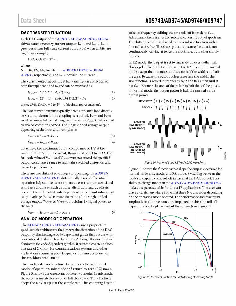
ANALOG MODES OF OPERATION The AD9743/AD9745/AD9746/AD9747 use a proprietary quad-switch architecture that lowers the distortion of the DAC output by eliminating a code dependent glitch that occurs with conventional dual-switch architectures. Although this architecture eliminates the code dependent glitches, it creates a constant glitch at a rate of 2 × fDAC. For communications systems and other applications requiring good frequency domain performance, this is seldom problematic.
The quad-switch architecture also supports two additional modes of operation; mix mode and return-to-zero (RZ) mode. Figure 34 shows the waveforms of these two modes. In mix mode, the output is inverted every other half clock cycle. This effectively chops the DAC output at the sample rate. This chopping has the
effect of frequency shifting the sinc roll-off from dc to fDAC. Additionally, there is a second subtle effect on the output spectrum. The shifted spectrum is shaped by a second sinc function with a first null at 2 × fDAC. This shaping occurs because the data is not continuously varying at twice the clock rate, but rather simply repeats.
In RZ mode, the output is set to midscale on every other half clock cycle. The output is similar to the DAC output in normal mode except that the output pulses are half the width and half the area. Because the output pulses have half the width, the sinc function is scaled in frequency by 2 and has a first null at 2 × fDAC. Because the area of the pulses is half that of the pulses in normal mode, the output power is half the normal mode output power.
D9D8D7D6D5D4D3D2D1 D10INPUT DATA
DAC CLK
4-SWITCHDAC OUTPUT
(fS MIX MODE)
4-SWITCHDAC OUTPUT(RETURN TOZERO MODE)
06
569-
02
6
t
t
Figure 34. Mix Mode and RZ Mode DAC Waveforms
Figure 35 shows the functions that shape the output spectrums for normal mode, mix mode, and RZ mode. Switching between the modes reshapes the sinc roll off inherent at the DAC output. This ability to change modes in the AD9743/AD9745/AD9746/AD9747 makes the parts suitable for direct IF applications. The user can place a carrier anywhere in the first three Nyquist zones depending on the operating mode selected. The performance and maximum amplitude in all three zones are impacted by this sinc roll off depending on the placement of the carrier (see Figure 35).
0
–10
–20
–30
–40
T(f
) (d
B)
0.5 1.5 2FS
NORMAL
RZ
MIX0
656
9-0
27
Figure 35. Transfer Function for Each Analog Operating Mode
AD9743/AD9745/AD9746/AD9747 Data Sheet
Rev. B | Page 28 of 30
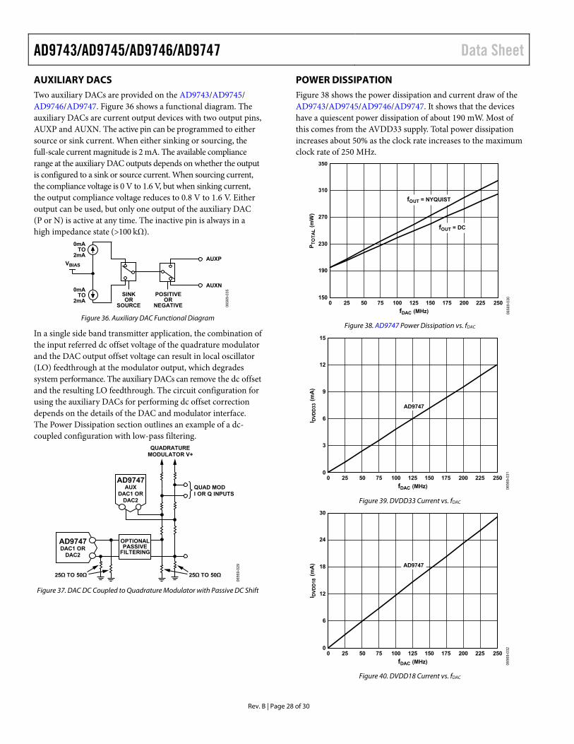
AUXILIARY DACS Two auxiliary DACs are provided on the AD9743/AD9745/ AD9746/AD9747. Figure 36 shows a functional diagram. The auxiliary DACs are current output devices with two output pins, AUXP and AUXN. The active pin can be programmed to either source or sink current. When either sinking or sourcing, the full-scale current magnitude is 2 mA. The available compliance range at the auxiliary DAC outputs depends on whether the output is configured to a sink or source current. When sourcing current, the compliance voltage is 0 V to 1.6 V, but when sinking current, the output compliance voltage reduces to 0.8 V to 1.6 V. Either output can be used, but only one output of the auxiliary DAC (P or N) is active at any time. The inactive pin is always in a high impedance state (>100 kΩ).
0656
9-03
5
VBIASAUXP
AUXNSINKOR
SOURCE
POSITIVEOR
NEGATIVE
0mATO
2mA
0mATO
2mA
Figure 36. Auxiliary DAC Functional Diagram
In a single side band transmitter application, the combination of the input referred dc offset voltage of the quadrature modulator and the DAC output offset voltage can result in local oscillator (LO) feedthrough at the modulator output, which degrades system performance. The auxiliary DACs can remove the dc offset and the resulting LO feedthrough. The circuit configuration for using the auxiliary DACs for performing dc offset correction depends on the details of the DAC and modulator interface. The Power Dissipation section outlines an example of a dc-coupled configuration with low-pass filtering.
AD9747AUX
DAC1 ORDAC2
AD9747DAC1 OR
DAC2
25Ω TO 50Ω
QUAD MODI OR Q INPUTS
QUADRATUREMODULATOR V+
25Ω TO 50Ω
0656
9-02
9
OPTIONALPASSIVE
FILTERING
Figure 37. DAC DC Coupled to Quadrature Modulator with Passive DC Shift
POWER DISSIPATION Figure 38 shows the power dissipation and current draw of the AD9743/AD9745/AD9746/AD9747. It shows that the devices have a quiescent power dissipation of about 190 mW. Most of this comes from the AVDD33 supply. Total power dissipation increases about 50% as the clock rate increases to the maximum clock rate of 250 MHz.
350
310
270
230
190
150
P TO
TAL
(mW
)0 50 100 150 200 250
fDAC (MHz) 0656
9-03
0
25 75 125 175 225
fOUT = DC
fOUT = NYQUIST
Figure 38. AD9747 Power Dissipation vs. fDAC
15
12
9
6
3
0
I DVD
D33
(mA
)
0 50 100 150 200 250fDAC (MHz) 06
569-
031
25 75 125 175 225
AD9747
Figure 39. DVDD33 Current vs. fDAC
30
24
18
12
6
0
I DVD
D18
(mA
)
0 50 100 150 200 250fDAC (MHz) 06
569-
032
25 75 125 175 225
AD9747
Figure 40. DVDD18 Current vs. fDAC
Data Sheet AD9743/AD9745/AD9746/AD9747
Rev. B | Page 29 of 30
15
13
11
9
7
5
I CVD
D18
(mA
)
0 50 100 150 200 250fDAC (MHz) 06
569-
033
25 75 125 175 225
Figure 41. CVDD18 Current vs. fDAC
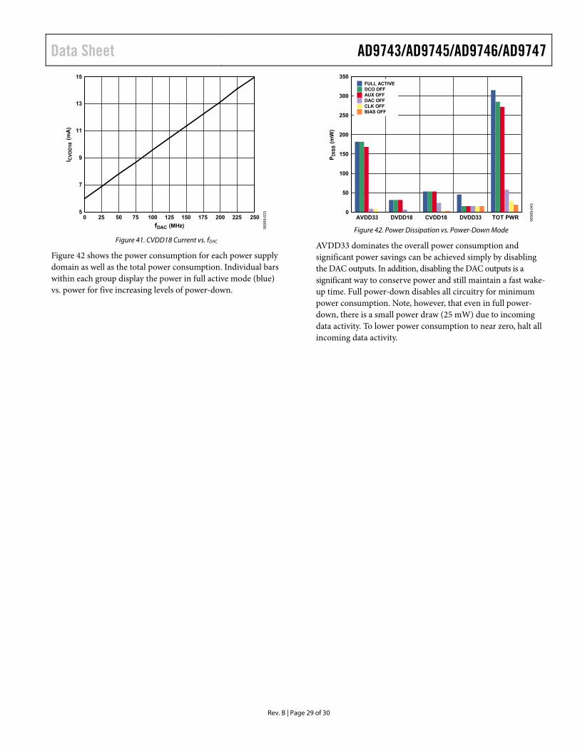
Figure 42 shows the power consumption for each power supply domain as well as the total power consumption. Individual bars within each group display the power in full active mode (blue) vs. power for five increasing levels of power-down.
0656
9-04
5
P DIS
S (m
W)
0
50
100
150
200
250
300
350
AVDD33 DVDD18 CVDD18 DVDD33 TOT PWR
FULL ACTIVEDCO OFFAUX OFFDAC OFFCLK OFFBIAS OFF
Figure 42. Power Dissipation vs. Power-Down Mode
AVDD33 dominates the overall power consumption and significant power savings can be achieved simply by disabling the DAC outputs. In addition, disabling the DAC outputs is a significant way to conserve power and still maintain a fast wake-up time. Full power-down disables all circuitry for minimum power consumption. Note, however, that even in full power-down, there is a small power draw (25 mW) due to incoming data activity. To lower power consumption to near zero, halt all incoming data activity.
AD9743/AD9745/AD9746/AD9747 Data Sheet
Rev. B | Page 30 of 30
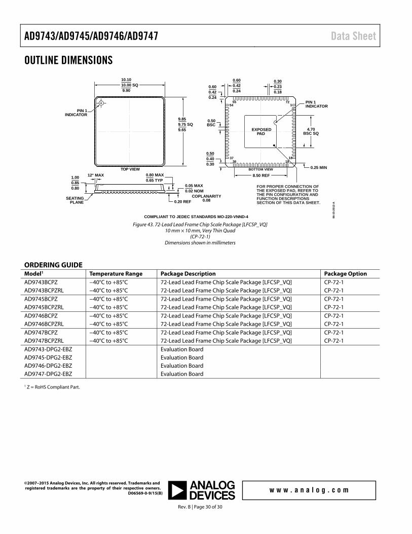
OUTLINE DIMENSIONS
COMPLIANT TO JEDEC STANDARDS MO-220-VNND-4
0.20 REF
0.80 MAX0.65 TYP
1.000.850.80
0.05 MAX0.02 NOM
1
18
54
371936
7255
0.500.400.30
8.50 REF
4.70BSC SQ
PIN 1INDICATOR
SEATINGPLANE
12° MAX
0.600.420.24
0.600.420.24
0.300.230.18
0.50BSC
PIN 1INDICATOR
COPLANARITY0.08
06-1
5-20
12-A
FOR PROPER CONNECTION OFTHE EXPOSED PAD, REFER TOTHE PIN CONFIGURATION ANDFUNCTION DESCRIPTIONSSECTION OF THIS DATA SHEET.
TOP VIEW
EXPOSEDPAD
BOTTOM VIEW
10.1010.00 SQ9.90
9.859.75 SQ9.65
0.25 MIN
Figure 43. 72-Lead Lead Frame Chip Scale Package [LFCSP_VQ]
10 mm × 10 mm, Very Thin Quad (CP-72-1)
Dimensions shown in millimeters
ORDERING GUIDE Model1 Temperature Range Package Description Package Option AD9743BCPZ −40°C to +85°C 72-Lead Lead Frame Chip Scale Package [LFCSP_VQ] CP-72-1 AD9743BCPZRL −40°C to +85°C 72-Lead Lead Frame Chip Scale Package [LFCSP_VQ] CP-72-1 AD9745BCPZ −40°C to +85°C 72-Lead Lead Frame Chip Scale Package [LFCSP_VQ] CP-72-1 AD9745BCPZRL −40°C to +85°C 72-Lead Lead Frame Chip Scale Package [LFCSP_VQ] CP-72-1 AD9746BCPZ −40°C to +85°C 72-Lead Lead Frame Chip Scale Package [LFCSP_VQ] CP-72-1 AD9746BCPZRL −40°C to +85°C 72-Lead Lead Frame Chip Scale Package [LFCSP_VQ] CP-72-1 AD9747BCPZ −40°C to +85°C 72-Lead Lead Frame Chip Scale Package [LFCSP_VQ] CP-72-1 AD9747BCPZRL −40°C to +85°C 72-Lead Lead Frame Chip Scale Package [LFCSP_VQ] CP-72-1 AD9743-DPG2-EBZ Evaluation Board AD9745-DPG2-EBZ Evaluation Board AD9746-DPG2-EBZ Evaluation Board AD9747-DPG2-EBZ Evaluation Board 1 Z = RoHS Compliant Part.
©2007–2015 Analog Devices, Inc. All rights reserved. Trademarks and registered trademarks are the property of their respective owners. D06569-0-9/15(B)