Embed Size (px)
Citation preview
12-Bit, 80 MSPS/105 MSPS/125 MSPS, 1.8 V Analog-to-Digital Converter
AD9233
Rev. A Information furnished by Analog Devices is believed to be accurate and reliable. However, no responsibility is assumed by Analog Devices for its use, nor for any infringements of patents or other rights of third parties that may result from its use. Specifications subject to change without notice. No license is granted by implication or otherwise under any patent or patent rights of Analog Devices. Trademarks and registered trademarks are the property of their respective owners.
One Technology Way, P.O. Box 9106, Norwood, MA 02062-9106, U.S.A.Tel: 781.329.4700 www.analog.com Fax: 781.461.3113 ©2006 Analog Devices, Inc. All rights reserved.
FEATURES 1.8 V analog supply operation 1.8 V to 3.3 V output supply SNR = 69.5 dBc (70.5 dBFS) to 70 MHz input SFDR = 85 dBc to 70 MHz input Low power: 395 mW @ 125 MSPS Differential input with 650 MHz bandwidth On-chip voltage reference and sample-and-hold amplifier DNL = ±0.15 LSB Flexible analog input: 1 V p-p to 2 V p-p range Offset binary, Gray code, or twos complement data format Clock duty cycle stabilizer Data output clock Serial port control
Built-in selectable digital test pattern generation Programmable clock and data alignment
APPLICATIONS Ultrasound equipment IF sampling in communications receivers
IS-95, CDMA-One, IMT-2000 Battery-powered instruments Hand-held scopemeters Low cost digital oscilloscopes
GENERAL DESCRIPTION
The AD9233 is a monolithic, single 1.8 V supply, 12-bit, 80 MSPS/ 105 MSPS/125 MSPS analog-to-digital converter (ADC), featuring a high performance sample-and-hold amplifier (SHA) and on-chip voltage reference. The product uses a multistage differential pipeline architecture with output error correction logic to provide 12-bit accuracy at 125 MSPS data rates and guarantees no missing codes over the full operating temperature range.
The wide bandwidth, truly differential SHA allows a variety of user-selectable input ranges and offsets, including single-ended applications. It is suitable for multiplexed systems that switch full-scale voltage levels in successive channels and for sampling single-channel inputs at frequencies well beyond the Nyquist rate. Combined with power and cost savings over previously available ADCs, the AD9233 is suitable for applications in communications, imaging, and medical ultrasound.
A differential clock input controls all internal conversion cycles. A duty cycle stabilizer (DCS) compensates for wide variations in the clock duty cycle while maintaining excellent overall ADC performance.
FUNCTIONAL BLOCK DIAGRAM DRVDDAVDD
AGND
0.5V
CLK– PDWN DRGND
OR
VIN+
VIN–
REFT
REFB
AD9233
VREF
SENSE
SHA
A/D
MDAC1
4 8
13
3
A/D8-STAGE1 1/2-BIT PIPELINE
REFSELECT
CLK+
CLOCKDUTY CYCLESTABILIZER
MODESELECT
CORRECTION LOGIC
OUTPUT BUFFERS DCO
SCLK/DFSSDIO/DCSCSB
D11 (MSB)
D0 (LSB)
0549
2-00
1
Figure 1.
The digital output data is presented in offset binary, Gray code, or twos complement formats. A data output clock (DCO) is provided to ensure proper latch timing with receiving logic.
The AD9233 is available in a 48-lead LFCSP and is specified over the industrial temperature range (−40°C to +85°C).
PRODUCT HIGHLIGHTS
1. The AD9233 operates from a single 1.8 V power supply and features a separate digital output driver supply to accommodate 1.8 V to 3.3 V logic families.
2. The patented SHA input maintains excellent performance for input frequencies up to 225 MHz.
3. The clock DCS maintains overall ADC performance over a wide range of clock pulse widths.
4. A standard serial port interface supports various product features and functions, such as data formatting (offset binary, twos complement, or Gray coding), enabling the clock DCS, power-down, and voltage reference mode.
5. The AD9233 is pin compatible with the AD9246, allowing a simple migration from 12 bits to 14 bits.
AD9233
Rev. A | Page 2 of 44
TABLE OF CONTENTS Features .............................................................................................. 1
Applications....................................................................................... 1
General Description ......................................................................... 1
Functional Block Diagram .............................................................. 1
Product Highlights ........................................................................... 1
Revision History ............................................................................... 3
Specifications..................................................................................... 4
DC Specifications ......................................................................... 4
AC Specifications.......................................................................... 5
Digital Specifications ................................................................... 6
Switching Specifications .............................................................. 7
Timing Diagram ........................................................................... 7
Absolute Maximum Ratings............................................................ 8
Thermal Resistance ...................................................................... 8
ESD Caution.................................................................................. 8
Pin Configuration and Function Descriptions............................. 9
Equivalent Circuits ......................................................................... 10
Typical Performance Characteristics ........................................... 11
Theory of Operation ...................................................................... 15
Analog Input Considerations.................................................... 15
Voltage Reference ....................................................................... 17
Clock Input Considerations ...................................................... 18
Jitter Considerations .................................................................. 19
Power Dissipation and Standby Mode..................................... 20
Digital Outputs ........................................................................... 21
Timing ......................................................................................... 22
Serial Port Interface (SPI).............................................................. 23
Configuration Using the SPI..................................................... 23
Hardware Interface..................................................................... 23
Configuration Without the SPI ................................................ 23
Memory Map .................................................................................. 24
Reading the Memory Map Table.............................................. 24
Layout Considerations................................................................... 27
Power and Ground Recommendations ................................... 27
CML ............................................................................................. 27
RBIAS........................................................................................... 27
Reference Decoupling................................................................ 27
Evaluation Board ............................................................................ 28
Power Supplies ............................................................................ 28
Input Signals................................................................................ 28
Output Signals ............................................................................ 28
Default Operation and Jumper Selection Settings................. 29
Alternative Clock Configurations............................................ 29
Alternative Analog Input Drive Configuration...................... 30
Schematics ....................................................................................... 31
Evaluation Board Layouts ......................................................... 36
Bill of Materials (BOM)............................................................. 39
Outline Dimensions ....................................................................... 42
Ordering Guide .......................................................................... 42
AD9233
Rev. A | Page 3 of 44
REVISION HISTORY
8/06—Rev. 0 to Rev. A Updated Format.................................................................. Universal Added 80 MSPS .................................................................. Universal Deleted Figure 19, Figure 20, Figure 22, and Figure 23; Renumbered Sequentially ..............................................................11 Deleted Figure 24, Figure 25, and Figure 27 to Figure 29; Renumbered Sequentially ..............................................................12 Deleted Figure 31 and Figure 34; Renumbered Sequentially ....13 Deleted Figure 37, Figure 38, Figure 40, and Figure 41; Renumbered Sequentially ..............................................................14 Deleted Figure 46; Renumbered Sequentially .............................15 Deleted Figure 52; Renumbered Sequentially .............................16 Changes to Figure 40 ......................................................................16 Changes to Figure 46 ......................................................................18 Inserted Figure 54; Renumbered Sequentially ............................20 Changes to Digital Outputs Section .............................................21 Changes to Timing Section............................................................22 Added Data Clock Output (DCO) Section..................................22 Changes to Configuration Using the SPI Section and Configuration Without the SPI Section .......................................23 Changes to Table 15 ........................................................................25 Changes to Table 16 ........................................................................39 Changes to Ordering Guide...........................................................42
4/06—Revision 0: Initial Version
AD9233
Rev. A | Page 4 of 44
SPECIFICATIONS DC SPECIFICATIONS AVDD = 1.8 V; DRVDD = 2.5 V, maximum sample rate, 2 V p-p differential input, 1.0 V internal reference; AIN = −1.0 dBFS, DCS enabled, unless otherwise noted.
Table 1. AD9233BCPZ-80 AD9233BCPZ-105 AD9233BCPZ-125 Parameter Temp Min Typ Max Min Typ Max Min Typ Max Unit RESOLUTION Full 12 12 12 Bits ACCURACY
No Missing Codes Full Guaranteed Guaranteed Guaranteed Offset Error Full ±0.3 ±0.5 ±0.3 ±0.8 ±0.3 ±0.8 % FSR Gain Error Full ±0.2 ±4.7 ±0.2 ±4.9 ±0.2 ±3.9 % FSR Differential Nonlinearity (DNL)1 Full ±0.3 ±0.5 ±0.5 LSB 25°C ±0.2 ±0.2 ±0.2 LSB Integral Nonlinearity (INL)1 Full ±1.2 ±1.2 ±1.2 LSB 25°C ±0.5 ±0.5 ±0.5 LSB
TEMPERATURE DRIFT Offset Error Full ±15 ±15 ±15 ppm/°C Gain Error Full ±95 ±95 ±95 ppm/°C
INTERNAL VOLTAGE REFERENCE Output Voltage Error (1 V Mode) Full ±5 ±20 ±5 ±35 ±5 ±35 mV Load Regulation @ 1.0 mA Full 7 7 7 mV
INPUT REFERRED NOISE VREF = 1.0 V 25°C 0.34 0.34 0.34 LSB rms
ANALOG INPUT Input Span, VREF = 1.0 V Full 2 2 2 V p-p Input Capacitance2 Full 8 8 8 pF
REFERENCE INPUT RESISTANCE Full 6 6 6 kΩ POWER SUPPLIES
Supply Voltage AVDD Full 1.7 1.8 1.9 1.7 1.8 1.9 1.7 1.8 1.9 V DRVDD Full 1.7 3.3 3.6 1.7 3.3 3.6 1.7 3.3 3.6 V
Supply Current IAVDD1 Full 138 155 178 194 220 236 mA IDRVDD1 (DRVDD = 1.8 V) Full 7 8 10 mA IDRVDD1 (DRVDD = 3.3 V) Full 12 14 17 mA
POWER CONSUMPTION DC Input Full 248 279 320 350 395 425 mW Sine Wave Input1 (DRVDD = 1.8 V) Full 261 335 415 mW Sine Wave Input1 (DRVDD = 3.3 V) Full 288 365 452 mW Standby3 Full 40 40 40 mW Power-Down Full 1.8 1.8 1.8 mW
1 Measured with a low input frequency, full-scale sine wave, with approximately 5 pF loading on each output bit. 2 Input capacitance refers to the effective capacitance between one differential input pin and AGND. Refer to Figure 4 for the equivalent analog input structure. 3 Standby power is measured with a dc input, the CLK pin inactive (set to AVDD or AGND).
AD9233
Rev. A | Page 5 of 44
AC SPECIFICATIONS AVDD = 1.8 V; DRVDD = 2.5 V, maximum sample rate, 2 V p-p differential input, 1.0 V internal reference; AIN = −1.0 dBFS, DCS enabled, unless otherwise noted.
Table 2. AD9233BCPZ-80 AD9233BCPZ-105 AD9233BCPZ-125 Parameter1 Temp Min Typ Max Min Typ Max Min Typ Max Unit SIGNAL-TO-NOISE-RATIO (SNR)
fIN = 2.4 MHz 25°C 69.5 69.5 69.5 dBc fIN = 70 MHz 25°C 69.5 69.5 69.5 dBc Full 68.9 68.3 68.3 dBc fIN = 100 MHz 25°C 69.4 69.4 69.4 dBc fIN = 170 MHz 25°C 68.9 68.9 68.9 dBc
SIGNAL-TO-NOISE AND DISTORTION (SINAD) fIN = 2.4 MHz 25°C 69.2 69.2 69.2 dBc fIN = 70 MHz 25°C 69.2 69.2 69.2 dBc Full 68.5 67.3 67.3 dBc fIN = 100 MHz 25°C 69.1 69.1 69.1 dBc fIN = 170 MHz 25°C 68.6 68.6 68.6 dBc
EFFECTIVE NUMBER OF BITS (ENOB) fIN = 2.4 MHz 25°C 11.4 11.4 11.4 Bits fIN = 70 MHz 25°C 11.4 11.4 11.4 Bits fIN = 100 MHz 25°C 11.4 11.4 11.4 Bits fIN = 170 MHz 25°C 11.3 11.3 11.3 Bits
WORST SECOND OR THIRD HARMONIC fIN = 2.4 MHz 25°C −90.0 −90.0 −90.0 dBc fIN = 70 MHz 25°C −85.0 −85.0 −85.0 dBc Full −76.0 −73.0 −73.0 dBc fIN = 100 MHz 25°C −85.0 −85.0 −85.0 dBc fIN = 170 MHz 25°C −83.5 −83.5 −83.5 dBc
SPURIOUS-FREE DYNAMIC RANGE (SFDR) fIN = 2.4 MHz 25°C 90.0 90.0 90.0 dBc fIN = 70 MHz 25°C 85.0 85.0 85.0 dBc Full 76.0 73.0 73.0 dBc fIN = 100 MHz 25°C 85.0 85.0 85.0 dBc fIN = 170 MHz 25°C 83.5 83.5 83.5 dBc
WORST OTHER (HARMONIC OR SPUR) fIN = 2.4 MHz 25°C −90.0 −90.0 −90.0 dBc fIN = 70 MHz 25°C −90.0 −90.0 −90.0 dBc Full −85.0 −81.0 −81.0 dBc fIN = 100 MHz 25°C −90.0 −90.0 −90.0 dBc fIN = 170 MHz 25°C −90.0 −90.0 −90.0 dBc
TWO-TONE SFDR fIN = 30 MHz (−7 dBFS), 31 MHz (−7 dBFS) 25°C 87 87 85 dBFS fIN = 170 MHz (−7 dBFS), 171 MHz (−7 dBFS) 25°C 83 83 84 dBFS
ANALOG INPUT BANDWIDTH 25°C 650 650 650 MHz 1 See AN-835, Understanding High Speed ADC Testing and Evaluation, for a complete set of definitions.
AD9233
Rev. A | Page 6 of 44
DIGITAL SPECIFICATIONS AVDD = 1.8 V; DRVDD = 2.5 V, maximum sample rate, 2 V p-p differential input, 1.0 V internal reference; AIN = −1.0 dBFS, DCS enabled, unless otherwise noted.
Table 3. AD9233BCPZ-80/105/125 Parameter Temp Min Typ Max Unit DIFFERENTIAL CLOCK INPUTS (CLK+, CLK−)
Logic Compliance CMOS/LVDS/LVPECL Internal Common-Mode Bias Full 1.2 V Differential Input Voltage Full 0.2 6 V p-p Input Voltage Range Full AVDD − 0.3 AVDD + 1.6 V Input Common-Mode Range Full 1.1 AVDD V High Level Input Voltage (VIH) Full 1.2 3.6 V Low Level Input Voltage (VIL) Full 0 0.8 V High Level Input Current (IIH) Full −10 +10 μA Low Level Input Current (IIL) Full −10 +10 μA Input Resistance Full 8 10 12 kΩ Input Capacitance Full 4 pF
LOGIC INPUTS (SCLK/DFS, OE, PWDN) High Level Input Voltage (VIH) Full 1.2 3.6 V Low Level Input Voltage (VIL) Full 0 0.8 V High Level Input Current (IIH) Full −50 −75 μA Low Level Input Current (IIL) Full −10 +10 μA Input Resistance Full 30 kΩ Input Capacitance Full 2 pF
LOGIC INPUTS (CSB) High Level Input Voltage (VIH) Full 1.2 3.6 V Low Level Input Voltage (VIL) Full 0 0.8 V High Level Input Current (IIH) Full −10 +10 μA Low Level Input Current (IIL) Full +40 +135 μA Input Resistance Full 26 kΩ Input Capacitance Full 2 pF
LOGIC INPUTS (SDIO/DCS) High Level Input Voltage (VIH) Full 1.2 DRVDD + 0.3 V Low Level Input Voltage (VIL) Full 0 0.8 V High Level Input Current (IIH) Full −10 +10 μA Low Level Input Current (IIL) Full +40 +130 μA Input Resistance Full 26 kΩ Input Capacitance Full 5 pF
DIGITAL OUTPUTS DRVDD = 3.3 V
High Level Output Voltage (VOH, IOH = 50 μA) Full 3.29 V High Level Output Voltage (VOH, IOH = 0.5 mA) Full 3.25 V Low Level Output Voltage (VOL, IOL = 1.6 mA) Full 0.2 V Low Level Output Voltage (VOL, IOL = 50 μA) Full 0.05 V
DRVDD = 1.8 V High Level Output Voltage (VOH, IOH = 50 μA) Full 1.79 V High Level Output Voltage (VOH, IOH = 0.5 mA) Full 1.75 V Low Level Output Voltage (VOL, IOL = 1.6 mA) Full 0.2 V Low Level Output Voltage (VOL, IOL = 50 μA) Full 0.05 V
AD9233
Rev. A | Page 7 of 44
SWITCHING SPECIFICATIONS AVDD = 1.8 V, DRVDD = 2.5 V, unless otherwise noted.
Table 4. AD9233BCPZ-80 AD9233BCPZ-105 AD9233BCPZ-125 Parameter1 Temp Min Typ Max Min Typ Max Min Typ Max Unit CLOCK INPUT PARAMETERS
Conversion Rate, DCS Enabled Full 20 80 20 105 20 125 MSPS Conversion Rate, DCS Disabled Full 10 80 10 105 10 125 MSPS CLK Period Full 12.5 9.5 8 ns CLK Pulse Width High, DCS Enabled Full 3.75 6.25 8.75 2.85 4.75 6.65 2.4 4 5.6 ns CLK Pulse Width High, DCS Disabled Full 5.63 6.25 6.88 4.28 4.75 5.23 3.6 4 4.4 ns
DATA OUTPUT PARAMETERS Data Propagation Delay (tPD)2 Full 3.1 3.9 4.8 3.1 3.9 4.8 3.1 3.9 4.8 ns DCO Propagation Delay (tDCO) Full 4.4 4.4 4.4 ns Setup Time (tS) Full 4.9 5.7 3.4 4.3 2.6 3.5 ns Hold Time (tH) Full 5.9 6.8 4.4 5.3 3.7 4.5 ns Pipeline Delay (Latency) Full 12 12 12 cycles Aperture Delay (tA) Full 0.8 0.8 0.8 ns Aperture Uncertainty (Jitter, tJ) Full 0.1 0.1 0.1 ps rms Wake-Up Time3 Full 350 350 350 ms
OUT-OF-RANGE RECOVERY TIME Full 2 2 3 cycles SERIAL PORT INTERFACE4
SCLK Period (tCLK) Full 40 40 40 ns SCLK Pulse Width High Time (tHI) Full 16 16 16 ns SCLK Pulse Width Low Time (tLO) Full 16 16 16 ns SDIO to SCLK Setup Time (tDS) Full 5 5 5 ns SDIO to SCLK Hold Time (tDH) Full 2 2 2 ns CSB to SCLK Setup Time (tS) Full 5 5 5 ns CSB to SCLK Hold Time (tH) Full 2 2 2 ns
1 See AN-835, Understanding High Speed ADC Testing and Evaluation, for a complete set of definitions. 2 Output propagation delay is measured from CLK 50% transition to DATA 50% transition, with 5 pF load. 3 Wake-up time is dependant on the value of the decoupling capacitors, values shown with 0.1 μF capacitor across REFT and REFB. 4 See Figure 57 and the Serial Port Interface (SPI) section.
TIMING DIAGRAM
CLK+
DCO
DATA
N
N + 1 N + 2N + 3
N + 4
N + 5N + 6 N + 7
N + 8
N – 12 N – 11 N – 10 N – 9 N – 8 N – 7 N – 6 N – 5 N – 4N – 13
CLK–
tCLK
tPD
tS tH tDCO tCLK
tA
0549
2-08
3
Figure 2. Timing Diagram
AD9233
Rev. A | Page 8 of 44
ABSOLUTE MAXIMUM RATINGS Table 5. Parameter Rating ELECTRICAL
AVDD to AGND −0.3 V to +2.0 V DRVDD to DRGND −0.3 V to +3.9 V AGND to DRGND −0.3 V to +0.3 V AVDD to DRVDD −3.9 V to +2.0 V D0 through D11 to DRGND −0.3 V to DRVDD + 0.3 V DCO to DRGND −0.3 V to DRVDD + 0.3 V OR to DRGND −0.3 V to DRVDD + 0.3 V CLK+ to AGND −0.3 V to +3.9 V CLK− to AGND −0.3 V to +3.9 V VIN+ to AGND −0.3 V to AVDD + 1.3 V VIN− to AGND −0.3 V to AVDD + 1.3 V VREF to AGND −0.3 V to AVDD + 0.2 V SENSE to AGND −0.3 V to AVDD + 0.2 V REFT to AGND −0.3 V to AVDD + 0.2 V REFB to AGND −0.3 V to AVDD + 0.2 V SDIO/DCS to DRGND −0.3 V to DRVDD + 0.3 V PDWN to AGND −0.3 V to +3.9 V CSB to AGND −0.3 V to +3.9 V SCLK/DFS to AGND −0.3 V to +3.9 V OEB to AGND −0.3 V to +3.9 V
ENVIRONMENTAL Storage Temperature Range –65°C to +125°C Operating Temperature Range –40°C to +85°C Lead Temperature
(Soldering 10 Sec) 300°C
Junction Temperature 150°C
Stresses above those listed under Absolute Maximum Ratings may cause permanent damage to the device. This is a stress rating only; functional operation of the device at these or any other conditions above those indicated in the operational section of this specification is not implied. Exposure to absolute maximum rating conditions for extended periods may affect device reliability.
THERMAL RESISTANCE The exposed paddle must be soldered to the ground plane for the LFCSP package. Soldering the exposed paddle to the customer board increases the reliability of the solder joints, maximizing the thermal capability of the package.
Table 6. Package Type θJA θJC Unit 48-lead LFCSP (CP-48-3) 26.4 2.4 °C/W
Typical θJA and θJC are specified for a 4-layer board in still air. Airflow increases heat dissipation, effectively reducing θJA. In addition, metal in direct contact with the package leads from metal traces, and through holes, ground, and power planes, reduces the θJA.
ESD CAUTION ESD (electrostatic discharge) sensitive device. Electrostatic charges as high as 4000 V readily accumulate on the human body and test equipment and can discharge without detection. Although this product features proprietary ESD protection circuitry, permanent damage may occur on devices subjected to high energy electrostatic discharges. Therefore, proper ESD precautions are recommended to avoid performance degradation or loss of functionality.
AD9233
Rev. A | Page 9 of 44
PIN CONFIGURATION AND FUNCTION DESCRIPTIONS
13 14 15 16 17 18 19 20 21 22 23 24
D10
(MSB
) D11 OR
DR
GN
DD
RVD
DSD
IO/D
CS
SCLK
/DFS
CSB
AG
ND
AVD
DA
GN
DA
VDD
48 47 46 45 44 43 42 41 40 39 38 37
DR
VDD
DR
GN
DN
CN
CD
CO
OEB
AVD
DA
GN
DA
VDD
CLK
–C
LK+
AG
ND
123456789
101112
(LSB) D0D1D2D3D4D5
DRGNDDRVDD
D6D7D8D9
RBIASCMLAVDDAGNDVIN–VIN+AGNDREFTREFBVREFSENSE
35PDWN36
34333231302928272625
AD9233TOP VIEW
(Not to Scale)
PIN 0 (EXPOSED PADDLE): AGND
NC = NO CONNECT
PIN 1INDICATOR
0549
2-00
3
Figure 3. Pin Configuration
Table 7. Pin Function Description Pin No. Mnemonic Description 0, 21, 23, 29, 32, 37, 41
AGND Analog Ground. (Pin 0 is the exposed thermal pad on the bottom of the package.)
1 to 6, 9 to 14 D0 (LSB) to D11 (MSB) Data Output Bits. 7, 16, 47 DRGND Digital Output Ground. 8, 17, 48 DRVDD Digital Output Driver Supply (1.8 V to 3.3 V). 15 OR Out-of-Range Indicator. 18 SDIO/DCS Serial Port Interface (SPI)® Data Input/Output (Serial Port Mode); Duty Cycle Stabilizer Select
(External Pin Mode). See Table 10. 19 SCLK/DFS SPI Clock (Serial Port Mode); Data Format Select Pin (External Pin Mode). See Table 10. 20 CSB SPI Chip Select (Active Low). 22, 24, 33, 40, 42 AVDD Analog Power Supply.
25 SENSE Reference Mode Selection. See Table 9. 26 VREF Voltage Reference Input/Output. 27 REFB Differential Reference (−). 28 REFT Differential Reference (+). 30 VIN+ Analog Input Pin (+). 31 VIN– Analog Input Pin (−). 34 CML Common-Mode Level Bias Output. 35 RBIAS External Bias Resister Connection. A 10 kΩ resister must be connected between this pin and
analog ground (AGND). 36 PDWN Power-Down Function Select. 38 CLK+ Clock Input (+). 39 CLK– Clock Input (−). 43 OEB Output Enable (Active Low). 44 DCO Data Clock Output. 45, 46 NC No Connection.
AD9233
Rev. A | Page 10 of 44
EQUIVALENT CIRCUITS
VIN
0549
2-00
4
Figure 4. Equivalent Analog Input Circuit
1.2V10kΩ 10kΩ
CLK+ CLK–
AVDD
0549
2-00
5
Figure 5. Equivalent Clock Input Circuit
SDIO/DCS1kΩ
0549
2-00
6
DRVDD
Figure 6. Equivalent SDIO/DCS Input Circuit
0549
2-00
7
DRVDD
DRGND Figure 7. Equivalent Digital Output Circuit
0549
2-00
8
SCLK/DFSOEB
PDWN
1kΩ
30kΩ
Figure 8. Equivalent SCLK/DFS, OEB, PDWN Input Circuit
CSB1kΩ26kΩ
AVDD
0549
2-01
0
Figure 9. Equivalent CSB Input Circuit
SENSE1kΩ
0549
2-01
1
Figure 10. Equivalent SENSE Circuit
VREF
6kΩ
0549
2-01
2
AVDD
Figure 11. Equivalent VREF Circuit
AD9233
Rev. A | Page 11 of 44
TYPICAL PERFORMANCE CHARACTERISTICS AVDD = 1.8 V; DRVDD = 2.5 V; maximum sample rate, DCS enabled, 1 V internal reference; 2 V p-p differential input; AIN = −1.0 dBFS; 64k sample; TA = 25°C, unless otherwise noted. All figures show typical performance for all speed grades.
0
–20
–40
–60
–80
–100
–120
–1400 15.625 31.250 46.875 62.500
0549
2-01
3
AM
PLIT
UD
E (d
BFS
)
FREQUENCY (MHz)
125MSPS2.3MHz @ –1dBFSSNR = 69.5dBc (70.5dBFS)ENOB = 11.2 BITSSFDR = 90.0dBc
Figure 12. AD9233-125 Single-Tone FFT with FIN = 2.3 MHz
0
–20
–40
–60
–80
–100
–120
–1400 15.625 31.250 46.875 62.500
0549
2-01
4
AM
PLIT
UD
E (d
BFS
)
FREQUENCY (MHz)
125MSPS30.3MHz @ –1dBFSSNR = 69.5dBc (70.5dBFS)ENOB = 11.2 BITSSFDR = 88.8dBc
Figure 13. AD9233-125 Single-Tone FFT with FIN = 30.3 MHz
0
–20
–40
–60
–80
–100
–120
–1400 15.625 31.250 46.875 62.500
0549
2-01
5
AM
PLIT
UD
E (d
BFS
)
FREQUENCY (MHz)
125MSPS70.3MHz @ –1dBFSSNR = 69.5dBc (70.5dBFS)ENOB = 11.2 BITSSFDR = 85.0dBc
Figure 14. AD9233-125 Single-Tone FFT with FIN = 70.3 MHz
0
–20
–40
–60
–80
–100
–120
–1400 15.625 31.250 46.875 62.500
0549
2-01
6
AM
PLIT
UD
E (d
BFS
)
FREQUENCY (MHz)
125MSPS100.3MHz @ –1dBFSSNR = 69.4dBc (70.4dBFS)ENOB = 11.2 BITSSFDR = 85.0dBc
Figure 15. AD9233-125 Single-Tone FFT with FIN = 100.3 MHz
0
–20
–40
–60
–80
–100
–120
–1400 15.625 31.250 46.875 62.500
0549
2-01
7
AM
PLIT
UD
E (d
BFS
)
FREQUENCY (MHz)
125MSPS140.3MHz @ –1dBFSSNR = 69.0dBc (70.0dBFS)ENOB = 11.1 BITSSFDR = 85.0dBc
Figure 16. AD9233-125 Single-Tone FFT with FIN = 140.3 MHz
0
–20
–40
–60
–80
–100
–120
–1400 15.625 31.250 46.875 62.500
0549
2-01
8
AM
PLIT
UD
E (d
BFS
)
FREQUENCY (MHz)
125MSPS170.3MHz @ –1dBFSSNR = 68.9dBc (69.9dBFS)ENOB = 11.1 BITSSFDR = 83.5dBc
Figure 17. AD9233-125 Single-Tone FFT with FIN = 170.3 MHz
AD9233
Rev. A | Page 12 of 44
0
–20
–40
–60
–80
–100
–120
–1400 15.625 31.250 46.875 62.500
0549
2-01
9
AM
PLIT
UD
E (d
BFS
)
FREQUENCY (MHz)
125MSPS225.3MHz @ –1dBFSSNR = 68.5dBc (69.5dBFS)ENOB = 11.0 BITSSFDR = 80.4dBc
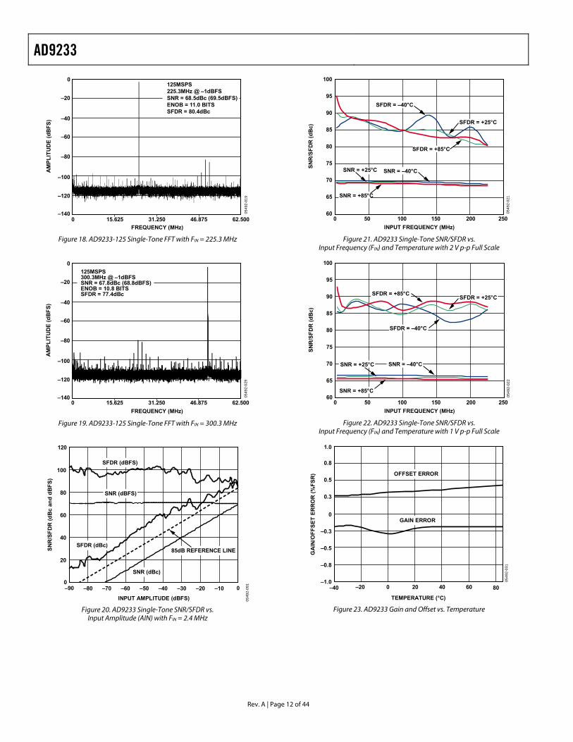
Figure 18. AD9233-125 Single-Tone FFT with FIN = 225.3 MHz
0
–20
–40
–60
–80
–100
–120
–1400 15.625 31.250 46.875 62.500
0549
2-02
9
AM
PLIT
UD
E (d
BFS
)
FREQUENCY (MHz)
125MSPS300.3MHz @ –1dBFSSNR = 67.8dBc (68.8dBFS)ENOB = 10.8 BITSSFDR = 77.4dBc
Figure 19. AD9233-125 Single-Tone FFT with FIN = 300.3 MHz
120
0–90 0
INPUT AMPLITUDE (dBFS)
SNR
/SFD
R (d
Bc
and
dBFS
)
SNR (dBFS)
SFDR (dBFS)
SNR (dBc)
SFDR (dBc)85dB REFERENCE LINE
100
80
60
40
20
–80 –70 –60 –50 –40 –30 –20 –10
0549
2-09
1
Figure 20. AD9233 Single-Tone SNR/SFDR vs.
Input Amplitude (AIN) with FIN = 2.4 MHz
100
90
95
85
80
75
70
65
600 15050 100 200 250
0549
2-02
1
SNR
/SFD
R (d
Bc)
INPUT FREQUENCY (MHz)
SNR = –40°CSNR = +25°C
SFDR = –40°C
SFDR = +85°C
SFDR = +25°C
SNR = +85°C
Figure 21. AD9233 Single-Tone SNR/SFDR vs.
Input Frequency (FIN) and Temperature with 2 V p-p Full Scale
100
90
95
85
80
75
70
65
600 15050 100 200 250
SNR
/SFD
R (d
Bc)
INPUT FREQUENCY (MHz)
0549
2-02
2
SFDR = –40°C
SFDR = +25°CSFDR = +85°C
SNR = +85°C
SNR = +25°C SNR = –40°C
Figure 22. AD9233 Single-Tone SNR/SFDR vs.
Input Frequency (FIN) and Temperature with 1 V p-p Full Scale
1.0
–1.0
–0.8
–0.5
–0.3
0
0.3
0.5
–40 80
TEMPERATURE (°C)
–20 0 20 40 60
GA
IN/O
FFSE
T ER
RO
R (%
FSR
)
0.8
OFFSET ERROR
GAIN ERROR
0549
2-03
1
Figure 23. AD9233 Gain and Offset vs. Temperature
AD9233
Rev. A | Page 13 of 44
0
–20
–40
–60
–80
–100
–120
–1400 15.625 31.250 46.875 62.500
0549
2-02
4
AM
PLIT
UD
E (d
BFS
)
FREQUENCY (MHz)
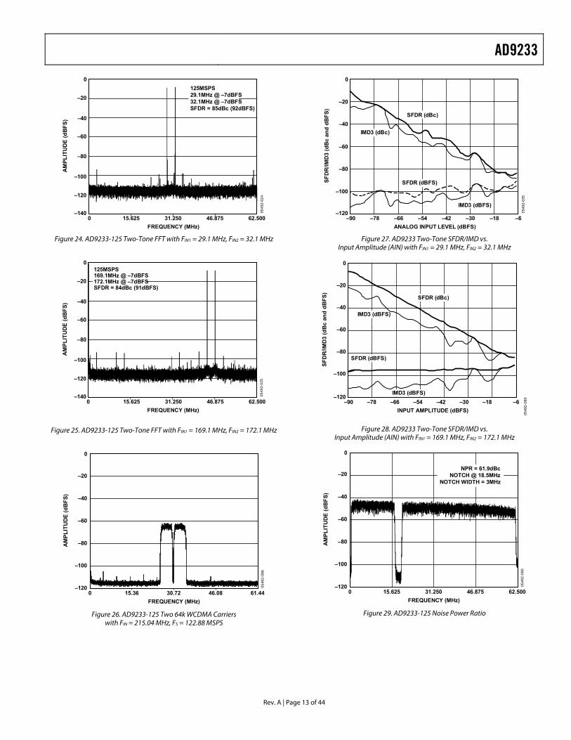
125MSPS29.1MHz @ –7dBFS32.1MHz @ –7dBFSSFDR = 85dBc (92dBFS)
Figure 24. AD9233-125 Two-Tone FFT with FIN1 = 29.1 MHz, FIN2 = 32.1 MHz
0
–20
–40
–60
–80
–100
–120
–1400 15.625 31.250 46.875 62.500
0549
2-02
5
AM
PLIT
UD
E (d
BFS
)
FREQUENCY (MHz)
125MSPS169.1MHz @ –7dBFS172.1MHz @ –7dBFSSFDR = 84dBc (91dBFS)
Figure 25. AD9233-125 Two-Tone FFT with FIN1 = 169.1 MHz, FIN2 = 172.1 MHz
0
–20
–40
–80
–100
–60
–1200 15.36 30.72 46.08 61.44
0549
2-08
6
AM
PLIT
UD
E (d
BFS
)
FREQUENCY (MHz) Figure 26. AD9233-125 Two 64k WCDMA Carriers
with FIN = 215.04 MHz, FS = 122.88 MSPS
0
–20
–40
–60
–80
–100
–120–90 –6–78 –66 –54 –42 –30 –18
0549
2-03
5
SFD
R/IM
D3
(dB
c an
d dB
FS)
ANALOG INPUT LEVEL (dBFS)
SFDR (dBFS)
IMD3 (dBFS)
IMD3 (dBc)
SFDR (dBc)
Figure 27. AD9233 Two-Tone SFDR/IMD vs.
Input Amplitude (AIN) with FIN1 = 29.1 MHz, FIN2 = 32.1 MHz
0
–20
–40
–60
–80
–100
–120–90 –78 –66 –54 –42 –30 –18 –6
SFD
R/IM
D3
(dB
c an
d dB
FS)
INPUT AMPLITUDE (dBFS)
SFDR (dBc)
SFDR (dBFS)
IMD3 (dBFS)
IMD3 (dBFS)
0549
2-08
0
Figure 28. AD9233 Two-Tone SFDR/IMD vs. Input Amplitude (AIN) with FIN1 = 169.1 MHz, FIN2 = 172.1 MHz
NPR = 61.9dBcNOTCH @ 18.5MHz
NOTCH WIDTH = 3MHz
0
–20
–40
–60
–80
–100
–1200 15.625 31.250 46.875 62.500
0549
2-09
0
AM
PLIT
UD
E (d
BFS
)
FREQUENCY (MHz) Figure 29. AD9233-125 Noise Power Ratio
AD9233
Rev. A | Page 14 of 44
0549
2-02
7
100
95
90
85
80
75
70
655 25 45 65 85 105 1
SNR
/SFD
R (d
Bc)
CLOCK FREQUENCY (MSPS)25
SNR
SFDR
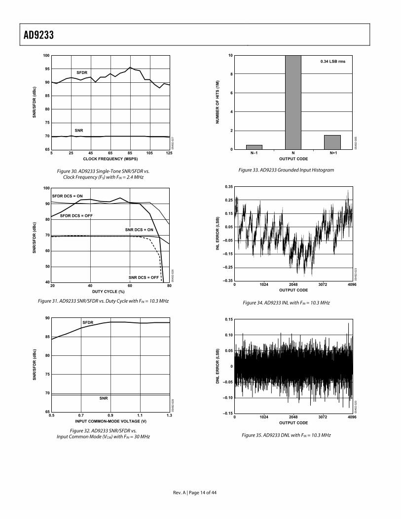
Figure 30. AD9233 Single-Tone SNR/SFDR vs. Clock Frequency (FS) with FIN = 2.4 MHz
100
90
80
70
60
50
4020 40 60 80
0549
2-02
6
SNR
/SFD
R (d
Bc)
DUTY CYCLE (%)
SFDR DCS = ON
SNR DCS = ON
SNR DCS = OFF
SFDR DCS = OFF
Figure 31. AD9233 SNR/SFDR vs. Duty Cycle with FIN = 10.3 MHz
90
85
80
75
70
650.5 0.7 0.9 1.1 1.3
0549
2-02
8
SNR
/SFD
R (d
Bc)
INPUT COMMON-MODE VOLTAGE (V)
SFDR
SNR
Figure 32. AD9233 SNR/SFDR vs. Input Common Mode (VCM) with FIN = 30 MHz
10
8
6
4
2
0N–1 N N+1
0549
2-08
5
NU
MB
ER O
F H
ITS
(1M
)
OUTPUT CODE
0.34 LSB rms
Figure 33. AD9233 Grounded Input Histogram
0.35
0.25
0.15
–0.05
0.05
–0.15
–0.25
–0.350 1024 2048 3072 4096
0549
2-02
3
INL
ERR
OR
(LSB
)
OUTPUT CODE
Figure 34. AD9233 INL with FIN = 10.3 MHz
0.15
0.10
0.05
0
–0.05
–0.10
–0.150 1024 2048 3072 4096
0549
2-02
0
DN
L ER
RO
R (L
SB)
OUTPUT CODE
Figure 35. AD9233 DNL with FIN = 10.3 MHz
AD9233
Rev. A | Page 15 of 44
THEORY OF OPERATION The AD9233 architecture consists of a front-end SHA followed by a pipelined switched capacitor ADC. The quantized outputs from each stage are combined into a final 12-bit result in the digital correction logic. The pipelined architecture permits the first stage to operate on a new input sample, while the remaining stages operate on preceding samples. Sampling occurs on the rising edge of the clock.
Each stage of the pipeline, excluding the last, consists of a low resolution flash ADC connected to a switched capacitor DAC and interstage residue amplifier (MDAC). The residue amplifier magnifies the difference between the reconstructed DAC output and the flash input for the next stage in the pipeline. One bit of redundancy is used in each stage to facilitate digital correction of flash errors. The last stage simply consists of a flash ADC.
The input stage contains a differential SHA that can be ac- or dc-coupled in differential or single-ended modes. The output-staging block aligns the data, carries out the error correction, and passes the data to the output buffers. The output buffers are powered from a separate supply, allowing adjustment of the output voltage swing. During power-down, the output buffers proceed into a high impedance state.
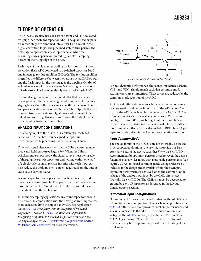
ANALOG INPUT CONSIDERATIONS The analog input to the AD9233 is a differential switched capacitor SHA that has been designed for optimum performance while processing a differential input signal.
The clock signal alternately switches the SHA between sample mode and hold mode (see Figure 36). When the SHA is switched into sample mode, the signal source must be capable of charging the sample capacitors and settling within one-half of a clock cycle. A small resistor in series with each input can help reduce the peak transient current required from the output stage of the driving source.
A shunt capacitor can be placed across the inputs to provide dynamic charging currents. This passive network creates a low-pass filter at the ADC input; therefore, the precise values are dependant upon the application.
In IF undersampling applications, any shunt capacitors should be reduced. In combination with the driving source impedance, these capacitors limit the input bandwidth. See Application Notes AN-742, Frequency Domain Response of Switched-Capacitor ADCs, and AN-827, A Resonant Approach To Interfacing Amplifiers to Switched-Capacitor ADCs, and the Analog Dialogue article, “Transformer-Coupled Front-End for Wideband A/D Converters”, for more information.
VIN+
VIN–
CPIN, PAR
CPIN, PAR
CS
CS
CH
CH
H
S
S
S
S 0549
2-03
7
Figure 36. Switched-Capacitor SHA Input
For best dynamic performance, the source impedances driving VIN+ and VIN− should match such that common-mode settling errors are symmetrical. These errors are reduced by the common-mode rejection of the ADC.
An internal differential reference buffer creates two reference voltages used to define the input span of the ADC core. The span of the ADC core is set by the buffer to be 2 × VREF. The reference voltages are not available to the user. Two bypass points, REFT and REFB, are brought out for decoupling to reduce the noise contributed by the internal reference buffer. It is recommended that REFT be decoupled to REFB by a 0.1 μF capacitor, as described in the Layout Considerations section.
Input Common Mode
The analog inputs of the AD9233 are not internally dc-biased. In ac-coupled applications, the user must provide this bias externally. Setting the device such that VCM = 0.55 × AVDD is recommended for optimum performance; however, the device functions over a wider range with reasonable performance (see Figure 32). An on-board common-mode voltage reference is included in the design and is available from the CML pin. Optimum performance is achieved when the common-mode voltage of the analog input is set by the CML pin voltage (typically 0.55 × AVDD). The CML pin must be decoupled to ground by a 0.1 μF capacitor, as described in the Layout Considerations section.
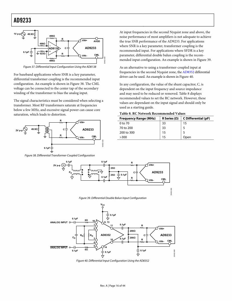
Differential Input Configurations
Optimum performance is achieved by driving the AD9233 in a differential input configuration. For baseband applications, the AD8138 differential driver provides excellent performance and a flexible interface to the ADC. The output common-mode voltage of the AD8138 is easily set with the CML pin of the AD9233 (see Figure 37), and the driver can be configured in a Sallen-Key filter topology to provide band limiting of the input signal.
AD9233
Rev. A | Page 16 of 44
0549
2-03
8
AVDD
1V p-p 49.9Ω
523Ω0.1µF
R
R
C
499Ω
499Ω
499Ω
AD8138 AD9233
VIN+
VIN– CML
Figure 37. Differential Input Configuration Using the AD8138
For baseband applications where SNR is a key parameter, differential transformer coupling is the recommended input configuration. An example is shown in Figure 38. The CML voltage can be connected to the center tap of the secondary winding of the transformer to bias the analog input.
The signal characteristics must be considered when selecting a transformer. Most RF transformers saturate at frequencies below a few MHz, and excessive signal power can cause core saturation, which leads to distortion.
0549
2-03
9
2V p-p 49.9Ω
0.1µF
R
R
C AD9233
VIN+
VIN– CML
Figure 38. Differential Transformer-Coupled Configuration
At input frequencies in the second Nyquist zone and above, the noise performance of most amplifiers is not adequate to achieve the true SNR performance of the AD9233. For applications where SNR is a key parameter, transformer coupling is the recommended input. For applications where SFDR is a key parameter, differential double balun coupling is the recom-mended input configuration. An example is shown in Figure 39.
As an alternative to using a transformer-coupled input at frequencies in the second Nyquist zone, the AD8352 differential driver can be used. An example is shown in Figure 40.
In any configuration, the value of the shunt capacitor, C, is dependent on the input frequency and source impedance and may need to be reduced or removed. Table 8 displays recommended values to set the RC network. However, these values are dependant on the input signal and should only be used as a starting guide.
Table 8. RC Network Recommended Values Frequency Range (MHz) R Series (Ω) C Differential (pF) 0 to 70 33 15 70 to 200 33 5 200 to 300 15 5 >300 15 Open
AD9233
R0.1µF0.1µF2V p-p VIN+
VIN– CML
C
R0.1µF
S0.1µF
0549
2-08
9
25Ω
25Ω
SPA P
Figure 39. Differential Double Balun Input Configuration
AD9233AD8352
0Ω
R
0Ω
CDRD RG
0.1µF
0.1µF
0.1µF
VIN+
VIN– CML
C
0.1µF
0.1µF
1612
345
11
R0.1µF
0.1µF
10
8, 13
14
VCC
200Ω
200Ω
0549
2-08
8
ANALOG INPUT
ANALOG INPUT
Figure 40. Differential Input Configuration Using the AD8352
AD9233
Rev. A | Page 17 of 44
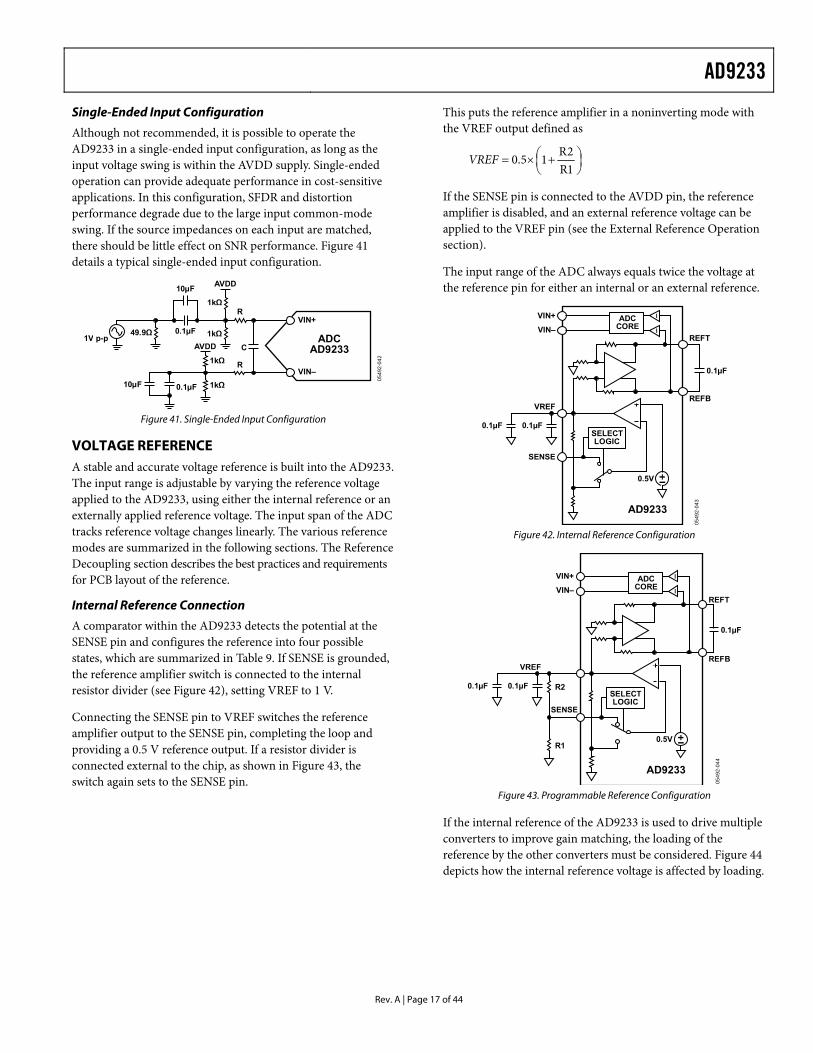
Single-Ended Input Configuration
Although not recommended, it is possible to operate the AD9233 in a single-ended input configuration, as long as the input voltage swing is within the AVDD supply. Single-ended operation can provide adequate performance in cost-sensitive applications. In this configuration, SFDR and distortion performance degrade due to the large input common-mode swing. If the source impedances on each input are matched, there should be little effect on SNR performance. Figure 41 details a typical single-ended input configuration.
0549
2-04
2
1V p-p
R
R
C
49.9Ω 0.1µF
10µF
10µF 0.1µF
AVDD
1kΩ
1kΩ
1kΩ
1kΩ
ADCAD9233
AVDD
VIN+
VIN–
Figure 41. Single-Ended Input Configuration
VOLTAGE REFERENCE A stable and accurate voltage reference is built into the AD9233. The input range is adjustable by varying the reference voltage applied to the AD9233, using either the internal reference or an externally applied reference voltage. The input span of the ADC tracks reference voltage changes linearly. The various reference modes are summarized in the following sections. The Reference Decoupling section describes the best practices and requirements for PCB layout of the reference.
Internal Reference Connection
A comparator within the AD9233 detects the potential at the SENSE pin and configures the reference into four possible states, which are summarized in Table 9. If SENSE is grounded, the reference amplifier switch is connected to the internal resistor divider (see Figure 42), setting VREF to 1 V.
Connecting the SENSE pin to VREF switches the reference amplifier output to the SENSE pin, completing the loop and providing a 0.5 V reference output. If a resistor divider is connected external to the chip, as shown in Figure 43, the switch again sets to the SENSE pin.
This puts the reference amplifier in a noninverting mode with the VREF output defined as
⎟⎠⎞
⎜⎝⎛ +×=
1R2R15.0VREF
If the SENSE pin is connected to the AVDD pin, the reference amplifier is disabled, and an external reference voltage can be applied to the VREF pin (see the External Reference Operation section).
The input range of the ADC always equals twice the voltage at the reference pin for either an internal or an external reference.
VREF
SENSE
0.5V
AD9233
REFT
REFB
SELECTLOGIC
0.1µF
0.1µF0.1µF
0549
2-04
3
VIN–
VIN+ ADCCORE
––
Figure 42. Internal Reference Configuration
VREF
SENSE
0.5V
AD9233
VIN–
VIN+
REFT
REFB
SELECTLOGIC
0.1µF0.1µF R2
R1
0549
2-04
4
0.1µF
ADCCORE
––
Figure 43. Programmable Reference Configuration
If the internal reference of the AD9233 is used to drive multiple converters to improve gain matching, the loading of the reference by the other converters must be considered. Figure 44 depicts how the internal reference voltage is affected by loading.
AD9233
Rev. A | Page 18 of 44
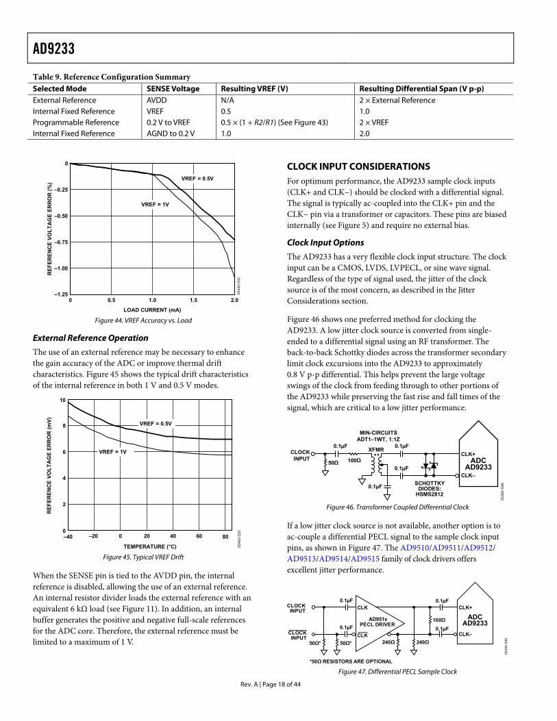
Table 9. Reference Configuration Summary Selected Mode SENSE Voltage Resulting VREF (V) Resulting Differential Span (V p-p) External Reference AVDD N/A 2 × External Reference Internal Fixed Reference VREF 0.5 1.0 Programmable Reference 0.2 V to VREF 0.5 × (1 + R2/R1) (See Figure 43) 2 × VREF Internal Fixed Reference AGND to 0.2 V 1.0 2.0
0
–1.250 2
LOAD CURRENT (mA)
REF
EREN
CE
VOLT
AG
E ER
RO
R (%
)
.0
–0.25
–0.50
–0.75
–1.00
0.5 1.0 1.5
VREF = 0.5V
VREF = 1V
0549
2-03
2
Figure 44. VREF Accuracy vs. Load
External Reference Operation
The use of an external reference may be necessary to enhance the gain accuracy of the ADC or improve thermal drift characteristics. Figure 45 shows the typical drift characteristics of the internal reference in both 1 V and 0.5 V modes.
–40 –20
10
0
TEMPERATURE (°C)
REF
EREN
CE
VOLT
AG
E ER
RO
R (m
V)
8
6
4
2
800 20 40 60
VREF = 0.5V
VREF = 1V
0549
2-03
3
Figure 45. Typical VREF Drift
When the SENSE pin is tied to the AVDD pin, the internal reference is disabled, allowing the use of an external reference. An internal resistor divider loads the external reference with an equivalent 6 kΩ load (see Figure 11). In addition, an internal buffer generates the positive and negative full-scale references for the ADC core. Therefore, the external reference must be limited to a maximum of 1 V.
CLOCK INPUT CONSIDERATIONS For optimum performance, the AD9233 sample clock inputs (CLK+ and CLK−) should be clocked with a differential signal. The signal is typically ac-coupled into the CLK+ pin and the CLK− pin via a transformer or capacitors. These pins are biased internally (see Figure 5) and require no external bias.
Clock Input Options
The AD9233 has a very flexible clock input structure. The clock input can be a CMOS, LVDS, LVPECL, or sine wave signal. Regardless of the type of signal used, the jitter of the clock source is of the most concern, as described in the Jitter Considerations section.
Figure 46 shows one preferred method for clocking the AD9233. A low jitter clock source is converted from single-ended to a differential signal using an RF transformer. The back-to-back Schottky diodes across the transformer secondary limit clock excursions into the AD9233 to approximately 0.8 V p-p differential. This helps prevent the large voltage swings of the clock from feeding through to other portions of the AD9233 while preserving the fast rise and fall times of the signal, which are critical to a low jitter performance.
0549
2-04
8
0.1µF
0.1µF
0.1µF0.1µF
SCHOTTKYDIODES:
HSMS2812
CLOCKINPUT
50Ω 100Ω
CLK–
CLK+ADC
AD9233
MIN-CIRCUITSADT1–1WT, 1:1Z
XFMR
Figure 46. Transformer Coupled Differential Clock
If a low jitter clock source is not available, another option is to ac-couple a differential PECL signal to the sample clock input pins, as shown in Figure 47. The AD9510/AD9511/AD9512/ AD9513/AD9514/AD9515 family of clock drivers offers excellent jitter performance.
CLOCKINPUT
100Ω0.1µF
0.1µF0.1µF
0.1µF
240Ω240Ω
CLOCKINPUT
0549
2-04
9
PECL DRIVER
50Ω* 50Ω*CLK
CLK
*50Ω RESISTORS ARE OPTIONAL
CLK–
CLK+
ADCAD9233AD951x
Figure 47. Differential PECL Sample Clock
AD9233
Rev. A | Page 19 of 44
A third option is to ac-couple a differential LVDS signal to the sample clock input pins, as shown in Figure 48. The AD9510/ AD9511/AD9512/AD9513/AD9514/AD9515 family of clock drivers offers excellent jitter performance.
0549
2-05
0
100Ω0.1µF
0.1µF0.1µF
0.1µF
50Ω*
LVDS DRIVER
50Ω*CLK
CLK
*50Ω RESISTORS ARE OPTIONAL
CLK–
CLK+
ADCAD9233
CLOCKINPUT
CLOCKINPUT
AD951x
Figure 48. Differential LVDS Sample Clock
In some applications, it is acceptable to drive the sample clock inputs with a single-ended CMOS signal. In such applications, directly drive CLK+ from a CMOS gate, while bypassing the CLK− pin to ground with a 0.1 μF capacitor. Although the CLK+ input circuit supply is AVDD (1.8 V), this input is designed to withstand input voltages up to 3.6 V, making the selection of the drive logic voltage very flexible. When driving CLK+ with a 1.8 V CMOS signal, it is required to bias the CLK− pin with a 0.1 μF capacitor in parallel with a 39 kΩ resistor (see Figure 49). The 39 kΩ resistor is not required when driving CLK+ with a 3.3 V CMOS signal (see Figure 50).
0549
2-05
1
CLOCKINPUT
0.1µF
0.1µF
0.1µF
39kΩ
AD951xCMOS DRIVER
50Ω*
OPTIONAL100Ω
*50Ω RESISTOR IS OPTIONAL
CLK–
CLK+
ADCAD9233
VCC
1kΩ
1kΩ
Figure 49. Single-Ended 1.8 V CMOS Sample Clock
0549
2-05
2
CLOCKINPUT
0.1µF
0.1µF
0.1µF
VCC
AD951xCMOS DRIVER
50Ω*
OPTIONAL100Ω
*50Ω RESISTOR IS OPTIONAL
CLK–
CLK+
ADCAD9233
1kΩ
1kΩ
Figure 50. Single-Ended 3.3 V CMOS Sample Clock
Clock Duty Cycle
Typical high speed ADCs use both clock edges to generate a variety of internal timing signals. As a result, these ADCs may be sensitive to clock duty cycle. Commonly, a ±5% tolerance is required on the clock duty cycle to maintain dynamic perform-ance characteristics.
The AD9233 contains a DCS that retimes the nonsampling, or falling edge, providing an internal clock signal with a nominal 50% duty cycle. This allows a wide range of clock input duty cycles without affecting the performance of the AD9233. Noise
and distortion performance are nearly flat for a wide range of duty cycles when the DCS is on, as shown in Figure 31.
Jitter in the rising edge of the input is still of paramount concern and is not reduced by the internal stabilization circuit. The duty cycle control loop does not function for clock rates less than 20 MHz nominally. The loop has a time constant associated with it that needs to be considered in applications where the clock rate can change dynamically, which requires a wait time of 1.5 μs to 5 μs after a dynamic clock frequency increase (or decrease) before the DCS loop is relocked to the input signal. During the time the loop is not locked, the DCS loop is bypassed, and the internal device timing is dependant on the duty cycle of the input clock signal. In such an application, it can be appropriate to disable the duty cycle stabilizer. In all other applications, enabling the DCS circuit is recommended to maximize ac performance.
The DCS can be enabled or disabled by setting the SDIO/DCS pin when operating in the external pin mode (see Table 10), or via the SPI, as described in the Table 15.
Table 10. Mode Selection (External Pin Mode) Voltage at Pin SCLK/DFS SDIO/DCS AGND Binary (default) DCS disabled AVDD Twos complement DCS enabled (default)
JITTER CONSIDERATIONS High speed, high resolution ADCs are sensitive to the quality of the clock input. The degradation in SNR at a given input frequency (FIN) due to jitter (tJ) is calculated as
SNR = −20 log (2π × FIN × tJ)
In the equation, the rms aperture jitter (tJ) represents the root-mean-square of all jitter sources, which include the clock input, analog input signal, and ADC aperture jitter specification. IF undersampling applications are particularly sensitive to jitter, as shown in Figure 51.
70
65
60
55
50
45
401 10 100 1000
0549
2-04
6
SNR
(dB
c)
INPUT FREQUENCY (MHz)
3.00ps
0.05ps
MEASUREDPERFORMANCE 0.20ps
0.5ps
1.0ps
1.50ps
2.00ps2.50ps
Figure 51. SNR vs. Input Frequency and Jitter
AD9233
Rev. A | Page 20 of 44
Treat the clock input as an analog signal in cases where aperture jitter may affect the dynamic range of the AD9233. Power supplies for clock drivers should be separated from the ADC output driver supplies to avoid modulating the clock signal with digital noise. The power supplies should also not be shared with analog input circuits such as buffers to avoid the clock modulating onto the input signal or vice versa. Low jitter, crystal-controlled oscillators make the best clock sources. If the clock is generated from another type of source (by gating, dividing, or other methods), it should be retimed by the original clock at the last step.
Refer to Application Notes AN-501, Aperture Uncertainty and ADC System Performance, and AN-756, Sampled Systems and the Effects of Clock Phase Noise and Jitter for more in-depth information about jitter performance as it relates to ADCs.
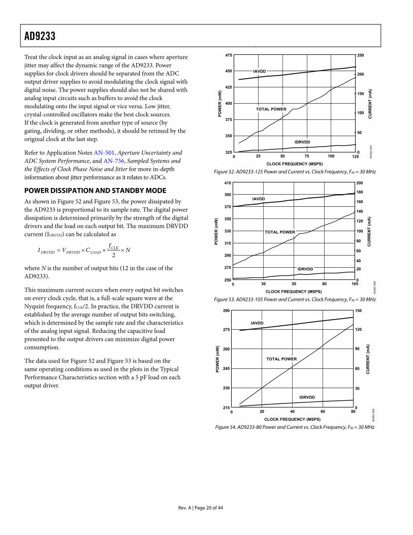
POWER DISSIPATION AND STANDBY MODE As shown in Figure 52 and Figure 53, the power dissipated by the AD9233 is proportional to its sample rate. The digital power dissipation is determined primarily by the strength of the digital drivers and the load on each output bit. The maximum DRVDD current (IDRVDD) can be calculated as
Nf
CVI CLKLOADDRVDDDRVDD ×××=
2
where N is the number of output bits (12 in the case of the AD9233).
This maximum current occurs when every output bit switches on every clock cycle, that is, a full-scale square wave at the Nyquist frequency, fCLK/2. In practice, the DRVDD current is established by the average number of output bits switching, which is determined by the sample rate and the characteristics of the analog input signal. Reducing the capacitive load presented to the output drivers can minimize digital power consumption.
The data used for Figure 52 and Figure 53 is based on the same operating conditions as used in the plots in the Typical Performance Characteristics section with a 5 pF load on each output driver.
475
3250 125
CLOCK FREQUENCY (MSPS)
POW
ER (m
W)
450
425
400
375
350
250
0
CU
RR
ENT
(mA
)
200
150
100
50
25 50 75 100
IDRVDD
IAVDD
TOTAL POWER
0549
2-03
4
Figure 52. AD9233-125 Power and Current vs. Clock Frequency, FIN = 30 MHz
410
2505
CLOCK FREQUENCY (MSPS)
POW
ER (m
W)
200
180
0
CU
RR
ENT
(mA
)
160
140
120
100
80
60
40
20
30 55 80 105
390
370
350
330
310
290
270 IDRVDD
IAVDD
TOTAL POWER
0549
2-08
2
Figure 53. AD9233-105 Power and Current vs. Clock Frequency, FIN = 30 MHz
290
2150
CLOCK FREQUENCY (MSPS)
POW
ER (m
W)
150
0
CU
RR
ENT
(mA
)
120
90
60
30
80
IDRVDD
IAVDD
TOTAL POWER
0549
2-09
3
275
260
245
230
20 40 60
Figure 54. AD9233-80 Power and Current vs. Clock Frequency, FIN = 30 MHz
AD9233
Rev. A | Page 21 of 44
Power-Down Mode
By asserting the PDWN pin high, the AD9233 is placed in power-down mode. In this state, the ADC typically dissipates 1.8 mW. During power-down, the output drivers are placed in a high impedance state. Reasserting the PDWN pin low returns the AD9233 to its normal operational mode. This pin is both 1.8 V and 3.3 V tolerant.
Low power dissipation in power-down mode is achieved by shutting down the reference, reference buffer, biasing networks, and clock. The decoupling capacitors on REFT and REFB are discharged when entering power-down mode and then must be recharged when returning to normal operation. As a result, the wake-up time is related to the time spent in power-down mode; shorter power-down cycles result in proportionally shorter wake-up times. With the recommended 0.1 μF decoupling capacitor on REFT and REFB, it takes approximately 0.25 ms to fully discharge the reference buffer decoupling capacitor and 0.35 ms to restore full operation.
Standby Mode
When using the SPI port interface, the user can place the ADC in power-down or standby modes. Standby mode allows the user to keep the internal reference circuitry powered when faster wake-up times are required. See the Memory Map section for more details.
DIGITAL OUTPUTS The AD9233 output drivers can be configured to interface with 1.8 V to 3.3 V logic families by matching DRVDD to the digital supply of the interfaced logic. The output drivers are sized to provide sufficient output current to drive a wide variety of logic families. However, large drive currents tend to cause current glitches on the supplies that can affect converter performance. Applications requiring the ADC to drive large capacitive loads or large fanouts can require external buffers or latches.
The output data format can be selected for either offset binary or twos complement by setting the SCLK/DFS pin when operating in the external pin mode (see Table 10). As detailed in the Interfacing to High Speed ADCs via SPI User Manual, the data format can be selected for either offset binary, twos complement, or Gray code when using the SPI control.
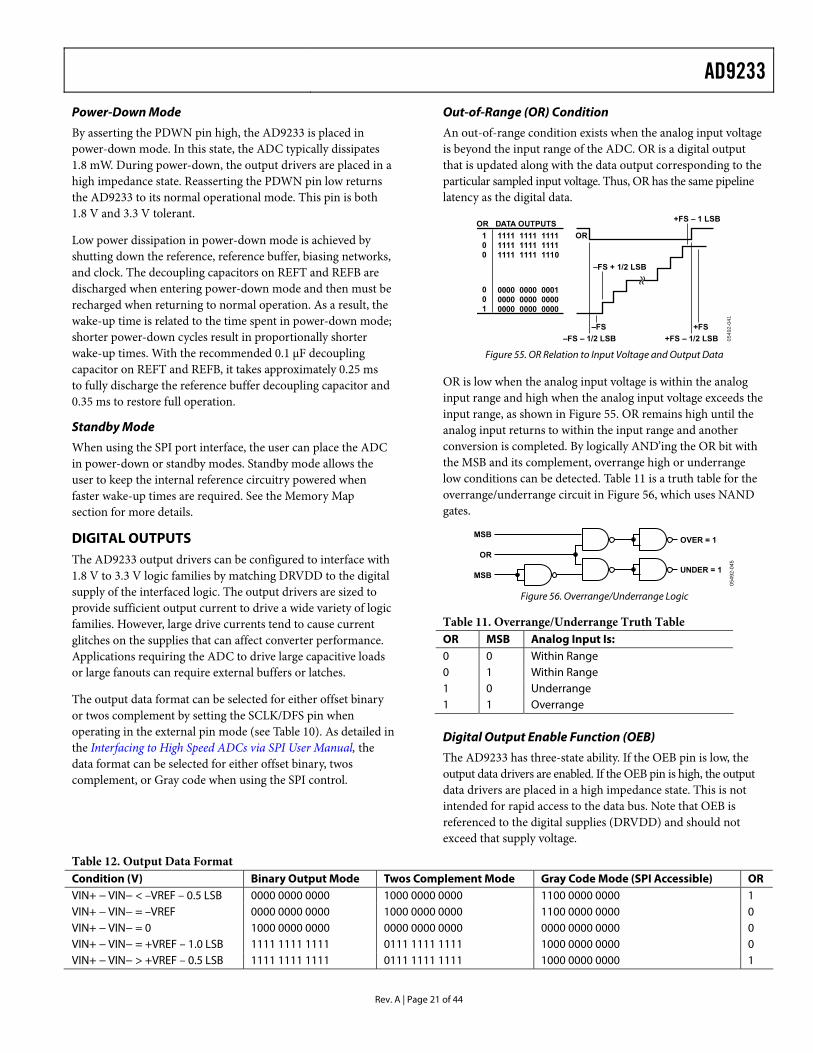
Out-of-Range (OR) Condition
An out-of-range condition exists when the analog input voltage is beyond the input range of the ADC. OR is a digital output that is updated along with the data output corresponding to the particular sampled input voltage. Thus, OR has the same pipeline latency as the digital data.
0549
2-04
1
100
001
OR DATA OUTPUTSOR
+FS – 1 LSB
+FS – 1/2 LSB+FS–FS
–FS + 1/2 LSB
–FS – 1/2 LSB
111111111111
111111111111
111111111110
000000000000
000000000000
000100000000
Figure 55. OR Relation to Input Voltage and Output Data
OR is low when the analog input voltage is within the analog input range and high when the analog input voltage exceeds the input range, as shown in Figure 55. OR remains high until the analog input returns to within the input range and another conversion is completed. By logically AND’ing the OR bit with the MSB and its complement, overrange high or underrange low conditions can be detected. Table 11 is a truth table for the overrange/underrange circuit in Figure 56, which uses NAND gates.
MSB
OR
MSB
OVER = 1
UNDER = 1
0549
2-04
5
Figure 56. Overrange/Underrange Logic
Table 11. Overrange/Underrange Truth Table OR MSB Analog Input Is: 0 0 Within Range 0 1 Within Range 1 0 Underrange 1 1 Overrange
Digital Output Enable Function (OEB)
The AD9233 has three-state ability. If the OEB pin is low, the output data drivers are enabled. If the OEB pin is high, the output data drivers are placed in a high impedance state. This is not intended for rapid access to the data bus. Note that OEB is referenced to the digital supplies (DRVDD) and should not exceed that supply voltage.
Table 12. Output Data Format Condition (V) Binary Output Mode Twos Complement Mode Gray Code Mode (SPI Accessible) OR VIN+ − VIN− < –VREF – 0.5 LSB 0000 0000 0000 1000 0000 0000 1100 0000 0000 1 VIN+ − VIN− = –VREF 0000 0000 0000 1000 0000 0000 1100 0000 0000 0 VIN+ − VIN− = 0 1000 0000 0000 0000 0000 0000 0000 0000 0000 0 VIN+ − VIN− = +VREF – 1.0 LSB 1111 1111 1111 0111 1111 1111 1000 0000 0000 0 VIN+ − VIN− > +VREF – 0.5 LSB 1111 1111 1111 0111 1111 1111 1000 0000 0000 1

AD9233
Rev. A | Page 22 of 44
TIMING The lowest typical conversion rate of the AD9233 is 10 MSPS. At clock rates below 10 MSPS, dynamic performance can degrade.
The AD9233 provides latched data outputs with a pipeline delay of 12 clock cycles. Data outputs are available one propagation delay (tPD) after the rising edge of the clock signal.
The length of the output data lines and the loads placed on them should be minimized to reduce transients within the AD9233. These transients can degrade the dynamic performance of the converter.
Data Clock Output (DCO)
The AD9233 provides a data clock output (DCO) intended for capturing the data in an external register. The data outputs are valid on the rising edge of DCO, unless the DCO clock polarity has been changed via the SPI. See Figure 2 for a graphical timing description.
AD9233
Rev. A | Page 23 of 44
SERIAL PORT INTERFACE (SPI) The AD9233 SPI allows the user to configure the converter for specific functions or operations through a structured register space provided inside the ADC. This provides the user added flexibility and customization depending on the application. Addresses are accessed via the serial port and can be written to or read from via the port. Memory is organized into bytes that are further divided into fields, as documented in the Memory Map section. For detailed operational information, see the Interfacing to High Speed ADCs via SPI User Manual.
CONFIGURATION USING THE SPI As summarized in Table 13, three pins define the SPI of this ADC. The SCLK/DFS pin synchronizes the read and write data presented to the ADC. The SDIO/DCS dual-purpose pin allows data to be sent and read from the internal ADC memory map registers. The CSB pin is an active low control that enables or disables the read and write cycles.
Table 13. Serial Port Interface Pins Mnemonic Description SCLK/DFS SCLK (Serial Clock) is the serial shift clock in. SCLK
synchronizes serial interface reads and writes. SDIO/DCS SDIO (Serial Data Input/Output) is a dual-purpose
pin. The typical role for this pin is an input and output depending on the instruction being sent and the relative position in the timing frame.
CSB CSB (Chip Select Bar) is an active low control that gates the read and write cycles.
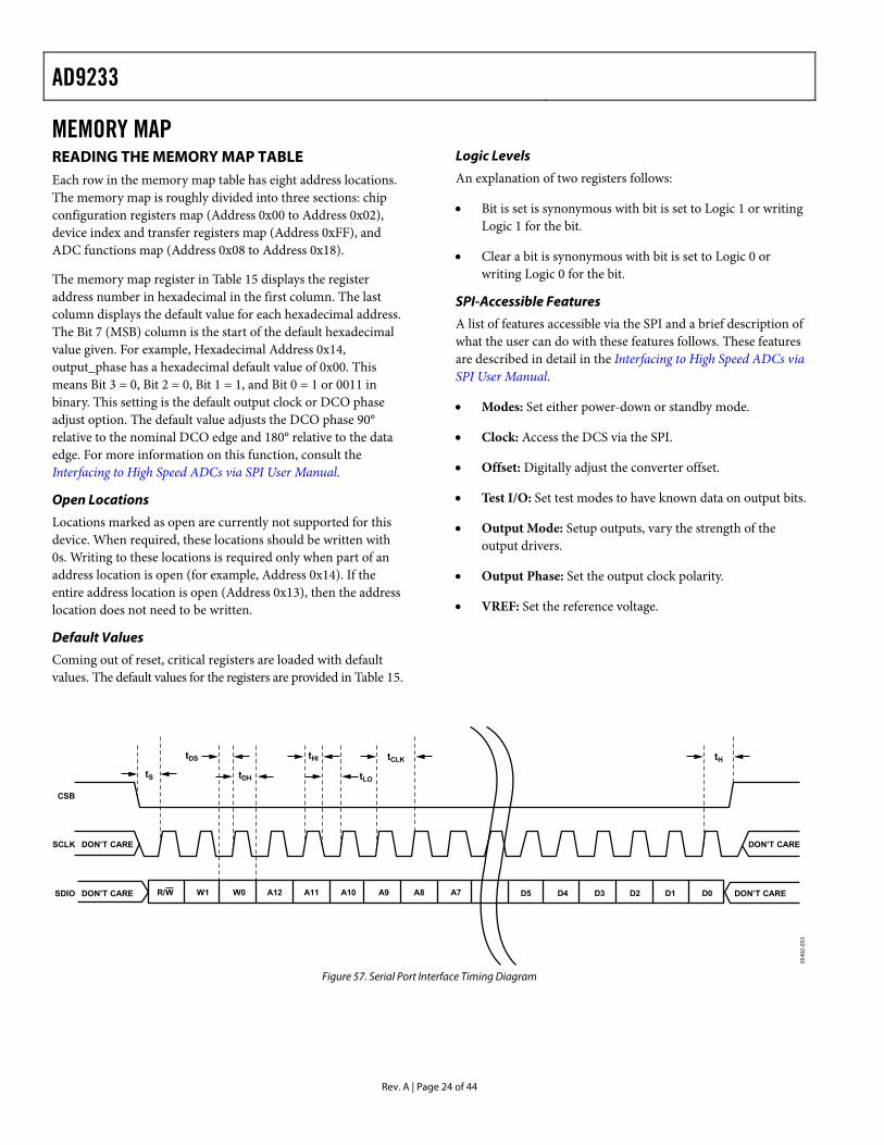
The falling edge of the CSB in conjunction with the rising edge of the SCLK determines the start of the framing. Figure 57 and Table 14 provide an example of the serial timing and its definitions.
Other modes involving the CSB are available. The CSB can be held low indefinitely, permanently enabling the device (this is called streaming). The CSB can stall high between bytes to allow for additional external timing. When CSB is tied high during power up, SPI functions are placed in a high impedance mode. This mode turns on any SPI pin secondary functions. If CSB is high at power up and then brought low to activate the SPI, the SPI pin secondary functions are no longer available, unless the device power is cycled.
During an instruction phase, a 16-bit instruction is transmitted. Data follows the instruction phase and the length is determined by the W0 bit and the W1 bit. All data is composed of 8-bit words. The first bit of each individual byte of serial data indicates whether a read or write command is issued. This allows the serial data input/output (SDIO) pin to change direction from an input to an output.
In addition to word length, the instruction phase determines if the serial frame is a read or write operation, allowing the serial port to be used to both program the chip as well as read the contents of the on-chip memory. If the instruction is a readback operation, performing a readback causes the serial data input/ output (SDIO) pin to change direction from an input to an output at the appropriate point in the serial frame.
Data can be sent in MSB first or in LSB first mode. MSB first is the default on power up and can be changed via the configuration register. For more information, see the Interfacing to High Speed ADCs via SPI User Manual.
Table 14. SPI Timing Diagram Specifications Name Description tDS Setup time between data and rising edge of SCLK tDH Hold time between data and rising edge of SCLK tCLK Period of the clock tS Setup time between CSB and SCLK tH Hold time between CSB and SCLK tHI Minimum period that SCLK should be in a logic high state tLO Minimum period that SCLK should be in a logic low state
HARDWARE INTERFACE The pins described in Table 13 comprise the physical interface between the user’s programming device and the serial port of the AD9233. The SCLK and CSB pins function as inputs when using the SPI interface. The SDIO pin is bidirectional, functioning as an input during write phases and as an output during readback.
The SPI interface is flexible enough to be controlled by either PROM or PIC microcontrollers. This provides the user with the ability to use an alternate method to program the ADC. One method is described in detail in the Application Note AN-812.
When the SPI interface is not used, some pins serve a dual function. When strapped to AVDD or ground during device power on, the pins are associated with a specific function.
CONFIGURATION WITHOUT THE SPI In applications that do not interface to the SPI control registers, the SDIO/DCS and SCLK/DFS pins serve as standalone CMOS-compatible control pins. When the device is powered up with the CSB chip select connected to AVDD, the serial port interface is disabled. In this mode, it is assumed that the user intends to use the pins as static control lines for the output data format and duty cycle stabilizer (see Table 10). For more information, see the Interfacing to High Speed ADCs via SPI User Manual.
AD9233
Rev. A | Page 24 of 44
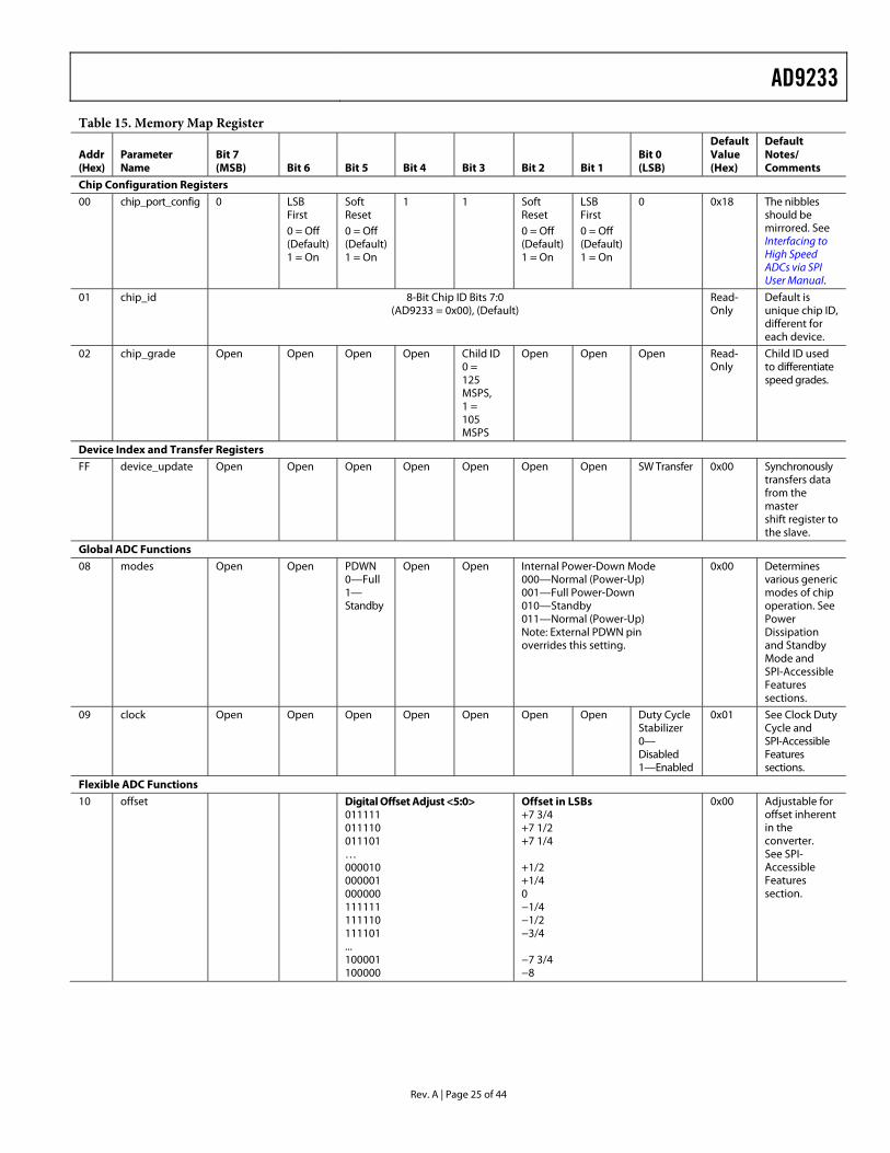
MEMORY MAP READING THE MEMORY MAP TABLE Each row in the memory map table has eight address locations. The memory map is roughly divided into three sections: chip configuration registers map (Address 0x00 to Address 0x02), device index and transfer registers map (Address 0xFF), and ADC functions map (Address 0x08 to Address 0x18).
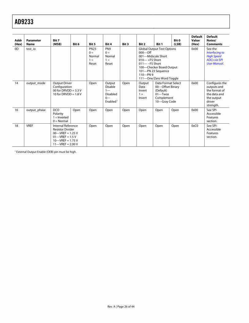
The memory map register in Table 15 displays the register address number in hexadecimal in the first column. The last column displays the default value for each hexadecimal address. The Bit 7 (MSB) column is the start of the default hexadecimal value given. For example, Hexadecimal Address 0x14, output_phase has a hexadecimal default value of 0x00. This means Bit 3 = 0, Bit 2 = 0, Bit 1 = 1, and Bit 0 = 1 or 0011 in binary. This setting is the default output clock or DCO phase adjust option. The default value adjusts the DCO phase 90° relative to the nominal DCO edge and 180° relative to the data edge. For more information on this function, consult the Interfacing to High Speed ADCs via SPI User Manual.
Open Locations
Locations marked as open are currently not supported for this device. When required, these locations should be written with 0s. Writing to these locations is required only when part of an address location is open (for example, Address 0x14). If the entire address location is open (Address 0x13), then the address location does not need to be written.
Default Values
Coming out of reset, critical registers are loaded with default values. The default values for the registers are provided in Table 15.
Logic Levels
An explanation of two registers follows:
• Bit is set is synonymous with bit is set to Logic 1 or writing Logic 1 for the bit.
• Clear a bit is synonymous with bit is set to Logic 0 or writing Logic 0 for the bit.
SPI-Accessible Features
A list of features accessible via the SPI and a brief description of what the user can do with these features follows. These features are described in detail in the Interfacing to High Speed ADCs via SPI User Manual.
• Modes: Set either power-down or standby mode.
• Clock: Access the DCS via the SPI.
• Offset: Digitally adjust the converter offset.
• Test I/O: Set test modes to have known data on output bits.
• Output Mode: Setup outputs, vary the strength of the output drivers.
• Output Phase: Set the output clock polarity.
• VREF: Set the reference voltage.
DON’T CARE
DON’T CAREDON’T CARE
DON’T CARE
SDIO
SCLK
CSB
tS tDH
tHI tCLK
tLO
tDS tH
R/W W1 W0 A12 A11 A10 A9 A8 A7 D5 D4 D3 D2 D1 D0
0549
2-05
3
Figure 57. Serial Port Interface Timing Diagram
AD9233
Rev. A | Page 25 of 44
Table 15. Memory Map Register
Addr (Hex)
Parameter Name
Bit 7 (MSB) Bit 6 Bit 5 Bit 4 Bit 3 Bit 2 Bit 1
Bit 0 (LSB)
DefaultValue (Hex)
Default Notes/ Comments
Chip Configuration Registers
00 chip_port_config 0 LSB First 0 = Off (Default) 1 = On
Soft Reset 0 = Off (Default)1 = On
1 1 Soft Reset 0 = Off (Default)1 = On
LSB First 0 = Off (Default)1 = On
0 0x18 The nibbles should be mirrored. See Interfacing to High Speed ADCs via SPI User Manual.
01 chip_id 8-Bit Chip ID Bits 7:0 (AD9233 = 0x00), (Default)
Read- Only
Default is unique chip ID,different for each device.
02 chip_grade Open Open Open Open Child ID 0 = 125 MSPS, 1 = 105 MSPS
Open Open Open Read- Only
Child ID used to differentiate speed grades.
Device Index and Transfer Registers
FF device_update Open Open Open Open Open Open Open SW Transfer 0x00 Synchronously transfers data from the master shift register to the slave.
Global ADC Functions
08 modes Open Open PDWN 0—Full 1— Standby
Open Open Internal Power-Down Mode 000—Normal (Power-Up) 001—Full Power-Down 010—Standby 011—Normal (Power-Up) Note: External PDWN pin overrides this setting.
0x00 Determines various genericmodes of chip operation. See Power Dissipation and Standby Mode and SPI-Accessible Features sections.
09 clock Open Open Open Open Open Open Open Duty Cycle Stabilizer 0—Disabled 1—Enabled
0x01 See Clock Duty Cycle and SPI-Accessible Features sections.
Flexible ADC Functions
10 offset Digital Offset Adjust <5:0> 011111 011110 011101 … 000010 000001 000000 111111 111110 111101 ... 100001 100000
Offset in LSBs +7 3/4 +7 1/2 +7 1/4 +1/2 +1/4 0 −1/4 −1/2 −3/4 −7 3/4 −8
0x00 Adjustable for offset inherent in the converter. See SPI-Accessible Features section.
AD9233
Rev. A | Page 26 of 44
Addr (Hex)
Parameter Name
Bit 7 (MSB) Bit 6 Bit 5 Bit 4 Bit 3 Bit 2 Bit 1
Bit 0 (LSB)
DefaultValue (Hex)
Default Notes/ Comments
0D test_io PN23 0 = Normal 1 = Reset
PN9 0 = Normal 1 = Reset
Global Output Test Options 000—Off 001—Midscale Short 010— +FS Short 011— −FS Short 100—Checker Board Output 101—PN 23 Sequence 110—PN 9 111—One/Zero Word Toggle
0x00 See the Interfacing to High Speed ADCs via SPI User Manual.
14 output_mode Output Driver Configuration 00 for DRVDD = 3.3 V 10 for DRVDD = 1.8 V
Open Output Disable 1— Disabled 0— Enabled1
Open Output Data Invert 1 = Invert
Data Format Select 00—Offset Binary (Default) 01—Twos Complement 10—Gray Code
0x00 Configures the outputs and the format of the data and the output driver strength.
16 output_phase DCO Polarity 1 = Inverted 0 = Normal
Open Open Open Open Open Open Open 0x00 See SPI-Accessible Features section.
18 VREF Internal Reference Resistor Divider 00—VREF = 1.25 V 01—VREF = 1.5 V 10—VREF = 1.75 V 11—VREF = 2.00 V
Open Open Open Open Open Open 0xC0 See SPI-Accessible Features section.
1 External Output Enable (OEB) pin must be high.
AD9233
Rev. A | Page 27 of 44
LAYOUT CONSIDERATIONS POWER AND GROUND RECOMMENDATIONS When connecting power to the AD9233, it is recommended that two separate supplies be used: one for analog (AVDD, 1.8 V nominal) and one for digital (DRVDD, 1.8 V to 3.3 V nominal). If only a single 1.8 V supply is available, then it should be routed to AVDD first, then tapped off and isolated with a ferrite bead or filter choke with decoupling capacitors preceding its con-nection to DRVDD. The user can employ several different decoupling capacitors to cover both high and low frequencies. These should be located close to the point of entry at the PC board level and close to the parts with minimal trace length.
A single PC board ground plane should be sufficient when using the AD9233. With proper decoupling and smart parti-tioning of the analog, digital, and clock sections of the board, optimum performance is easily achieved.
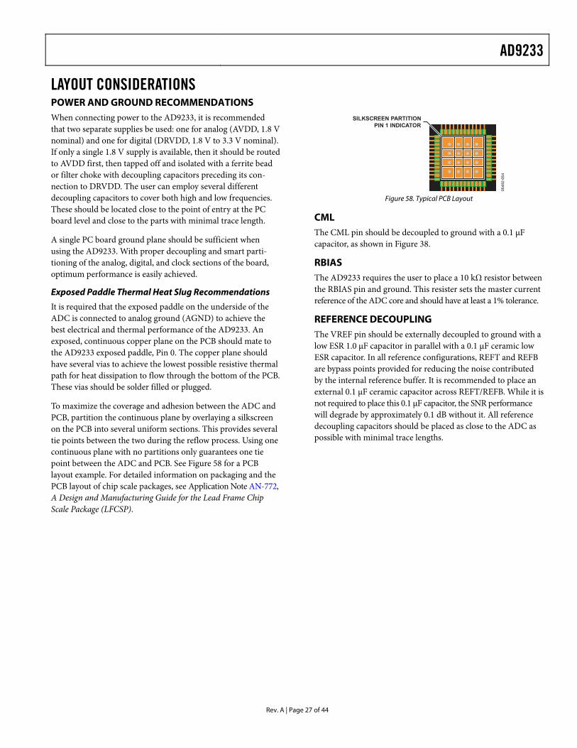
Exposed Paddle Thermal Heat Slug Recommendations
It is required that the exposed paddle on the underside of the ADC is connected to analog ground (AGND) to achieve the best electrical and thermal performance of the AD9233. An exposed, continuous copper plane on the PCB should mate to the AD9233 exposed paddle, Pin 0. The copper plane should have several vias to achieve the lowest possible resistive thermal path for heat dissipation to flow through the bottom of the PCB. These vias should be solder filled or plugged.
To maximize the coverage and adhesion between the ADC and PCB, partition the continuous plane by overlaying a silkscreen on the PCB into several uniform sections. This provides several tie points between the two during the reflow process. Using one continuous plane with no partitions only guarantees one tie point between the ADC and PCB. See Figure 58 for a PCB layout example. For detailed information on packaging and the PCB layout of chip scale packages, see Application Note AN-772, A Design and Manufacturing Guide for the Lead Frame Chip Scale Package (LFCSP).
SILKSCREEN PARTITIONPIN 1 INDICATOR
0549
2-05
4
Figure 58. Typical PCB Layout
CML The CML pin should be decoupled to ground with a 0.1 μF capacitor, as shown in Figure 38.
RBIAS The AD9233 requires the user to place a 10 kΩ resistor between the RBIAS pin and ground. This resister sets the master current reference of the ADC core and should have at least a 1% tolerance.
REFERENCE DECOUPLING The VREF pin should be externally decoupled to ground with a low ESR 1.0 μF capacitor in parallel with a 0.1 μF ceramic low ESR capacitor. In all reference configurations, REFT and REFB are bypass points provided for reducing the noise contributed by the internal reference buffer. It is recommended to place an external 0.1 μF ceramic capacitor across REFT/REFB. While it is not required to place this 0.1 μF capacitor, the SNR performance will degrade by approximately 0.1 dB without it. All reference decoupling capacitors should be placed as close to the ADC as possible with minimal trace lengths.
AD9233
Rev. A | Page 28 of 44
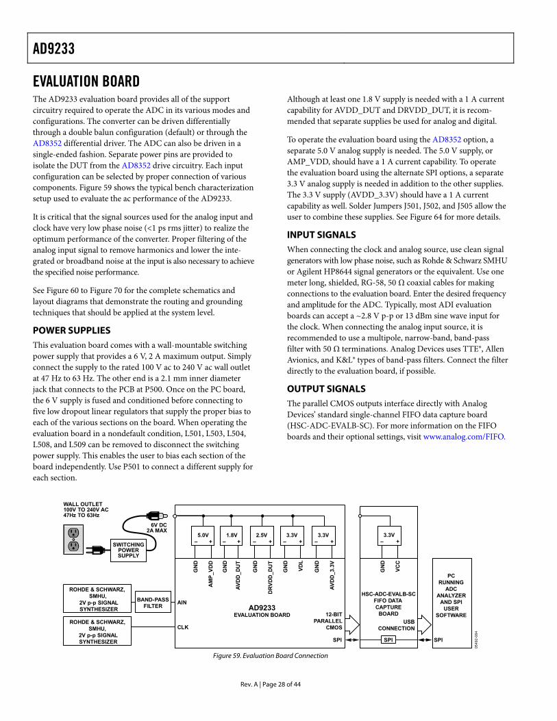
EVALUATION BOARD The AD9233 evaluation board provides all of the support circuitry required to operate the ADC in its various modes and configurations. The converter can be driven differentially through a double balun configuration (default) or through the AD8352 differential driver. The ADC can also be driven in a single-ended fashion. Separate power pins are provided to isolate the DUT from the AD8352 drive circuitry. Each input configuration can be selected by proper connection of various components. Figure 59 shows the typical bench characterization setup used to evaluate the ac performance of the AD9233.
It is critical that the signal sources used for the analog input and clock have very low phase noise (<1 ps rms jitter) to realize the optimum performance of the converter. Proper filtering of the analog input signal to remove harmonics and lower the inte-grated or broadband noise at the input is also necessary to achieve the specified noise performance.
See Figure 60 to Figure 70 for the complete schematics and layout diagrams that demonstrate the routing and grounding techniques that should be applied at the system level.
POWER SUPPLIES This evaluation board comes with a wall-mountable switching power supply that provides a 6 V, 2 A maximum output. Simply connect the supply to the rated 100 V ac to 240 V ac wall outlet at 47 Hz to 63 Hz. The other end is a 2.1 mm inner diameter jack that connects to the PCB at P500. Once on the PC board, the 6 V supply is fused and conditioned before connecting to five low dropout linear regulators that supply the proper bias to each of the various sections on the board. When operating the evaluation board in a nondefault condition, L501, L503, L504, L508, and L509 can be removed to disconnect the switching power supply. This enables the user to bias each section of the board independently. Use P501 to connect a different supply for each section.
Although at least one 1.8 V supply is needed with a 1 A current capability for AVDD_DUT and DRVDD_DUT, it is recom-mended that separate supplies be used for analog and digital.
To operate the evaluation board using the AD8352 option, a separate 5.0 V analog supply is needed. The 5.0 V supply, or AMP_VDD, should have a 1 A current capability. To operate the evaluation board using the alternate SPI options, a separate 3.3 V analog supply is needed in addition to the other supplies. The 3.3 V supply (AVDD_3.3V) should have a 1 A current capability as well. Solder Jumpers J501, J502, and J505 allow the user to combine these supplies. See Figure 64 for more details.
INPUT SIGNALS When connecting the clock and analog source, use clean signal generators with low phase noise, such as Rohde & Schwarz SMHU or Agilent HP8644 signal generators or the equivalent. Use one meter long, shielded, RG-58, 50 Ω coaxial cables for making connections to the evaluation board. Enter the desired frequency and amplitude for the ADC. Typically, most ADI evaluation boards can accept a ~2.8 V p-p or 13 dBm sine wave input for the clock. When connecting the analog input source, it is recommended to use a multipole, narrow-band, band-pass filter with 50 Ω terminations. Analog Devices uses TTE®, Allen Avionics, and K&L® types of band-pass filters. Connect the filter directly to the evaluation board, if possible.
OUTPUT SIGNALS The parallel CMOS outputs interface directly with Analog Devices’ standard single-channel FIFO data capture board (HSC-ADC-EVALB-SC). For more information on the FIFO boards and their optional settings, visit www.analog.com/FIFO.
ROHDE & SCHWARZ,SMHU,
2V p-p SIGNALSYNTHESIZER
ROHDE & SCHWARZ,SMHU,
2V p-p SIGNALSYNTHESIZER
BAND-PASSFILTER AIN
CLK
12-BITPARALLEL
CMOSUSB
CONNECTION
AD9233EVALUATION BOARD
HSC-ADC-EVALB-SCFIFO DATACAPTURE
BOARD
PCRUNNING
ADCANALYZER
AND SPIUSER
SOFTWARE
1.8V– +– +
AVD
D_D
UT
VDL
DR
VDD
_DU
T
GN
D
GN
D
– +5.0V
GN
D
AM
P_VD
D
2.5V
6V DC2A MAX
WALL OUTLET100V TO 240V AC47Hz TO 63Hz
SWITCHINGPOWERSUPPLY
– +
GN
D
3.3V
AVD
D_3
.3V
– +
GN
D
3.3V– +
VCC
GN
D
3.3V
SPI SPISPI
0549
2-08
4
Figure 59. Evaluation Board Connection
AD9233
Rev. A | Page 29 of 44
DEFAULT OPERATION AND JUMPER SELECTION SETTINGS The following is a list of the default and optional settings or modes allowed on the AD9233 Rev. A evaluation board.
POWER
Connect the switching power supply that is supplied in the evaluation kit between a rated 100 V ac to 240 V ac wall outlet at 47 Hz to 63 Hz and P500.
VIN
The evaluation board is set up for a double balun configuration analog input with optimum 50 Ω impedance matching out to 70 MHz. For more bandwidth response, the differential capacitor across the analog inputs can be changed or removed (see Table 8). The common mode of the analog inputs is developed from the center tap of the transformer via the CML pin of the ADC. See the Analog Input Considerations section for more information.
VREF
VREF is set to 1.0 V by tying the SENSE pin to ground via JP507 (Pin 1 and Pin 2). This causes the ADC to operate in 2.0 V p-p full-scale range. A separate external reference option is also included on the evaluation board. Simply connect JP507 between Pin 2 and Pin 3, connect JP501, and provide an external reference at E500. Proper use of the VREF options is detailed in the Voltage Reference section.
RBIAS
RBIAS requires a 10 kΩ (R503) to ground and is used to set the ADC core bias current.
CLOCK
The default clock input circuitry is derived from a simple transformer-coupled circuit using a high bandwidth 1:1 impedance ratio transformer (T503) that adds a very low amount of jitter to the clock path. The clock input is 50 Ω terminated and ac-coupled to handle single-ended sine wave inputs. The transformer converts the single-ended input to a differential signal that is clipped before entering the ADC clock inputs.
PDWN
To enable the power-down feature, connect JP506, shorting the PDWN pin to AVDD.
CSB
The CSB pin is internally pulled-up, setting the chip into external pin mode, to ignore the SDIO and SCLK information. To connect the control of the CSB pin to the SPI circuitry on the evaluation board, connect JP1 Pin 1 and Pin 2. To set the chip into serial pin mode and to enable the SPI information on the SDIO and SCLK pins, tie JP1 low (connect Pin 2 and Pin 3) in the always enabled mode.
SCLK/DFS
If the SPI port is in external pin mode, the SCLK/DFS pin sets the data format of the outputs. If the pin is left floating, the pin is internally pulled down, setting the default condition to binary. Connecting JP2 Pin 2 and Pin 3 sets the format to twos complement. If the SPI port is in serial pin mode, connecting JP2 Pin 1 and Pin 2 connects the SCLK pin to the on board SPI circuitry. See the Serial Port Interface (SPI) section for more details.
SDIO/DCS
If the SPI port is in external pin mode, the SDIO/DCS pin acts to set the duty cycle stabilizer. If the pin is left floating, the pin is internally pulled up, setting the default condition to DCS enabled. To disable the DCS, connect JP3 Pin 2 and Pin 3. If the SPI port is in serial pin mode, connecting JP3 Pin 1 and Pin 2 connects the SDIO pin to the on-board SPI circuitry. See the Serial Port Interface (SPI) section for more details.
ALTERNATIVE CLOCK CONFIGURATIONS A differential LVPECL clock can also be used to clock the ADC input using the AD9515 (U500). When using this drive option, the components listed in Table 16 need to be populated. Consult the AD9515 data sheet for further information.
To configure the analog input to drive the AD9515 instead of the default transformer option, the following components need to be added, removed, and/or changed.
• Remove R507, R508, C532, and C533 in the default clock path.
• Populate R505 with a 0 Ω resistor and C531 in the default clock path.
• Populate R511, R512, R513, R515 to R524, U500, R580, R582, R583, R584, C536, C537, and R586.
If using an oscillator, two oscillator footprint options are also available (OSC500) to check the performance of the ADC. JP508 provides the user flexibility in using the enable pin, which is common on most oscillators. Populate OSC500, R575, R587, and R588 to use this option.
AD9233
Rev. A | Page 30 of 44
ALTERNATIVE ANALOG INPUT DRIVE CONFIGURATION This section provides a brief description of the alternative analog input drive configuration using the AD8352 . When using this particular drive option, some components need to be populated as listed in Table 16. For more details on the AD8352 differential driver, including how it works and its optional pin settings, consult the AD8352 data sheet.
To configure the analog input to drive the AD8352 instead of the default transformer option, the following components need to be added, removed and/or changed:
• Remove C1 and C2 in the default analog input path.
• Populate R3 and R4 with 200 Ω resistors in the analog input path.
• Populate the optional amplifier input path with all components, except R594, R595, and C502. Note that to terminate the input path, only one of these components, (R9, R592, or R590 and R591) should be populated.
• Populate C529 with a 5 pF capacitor in the analog input path.
Currently, R561 and R562 are populated with 0 Ω resistors to allow signal connection. This area allows the user to design a filter if additional requirements are necessary.
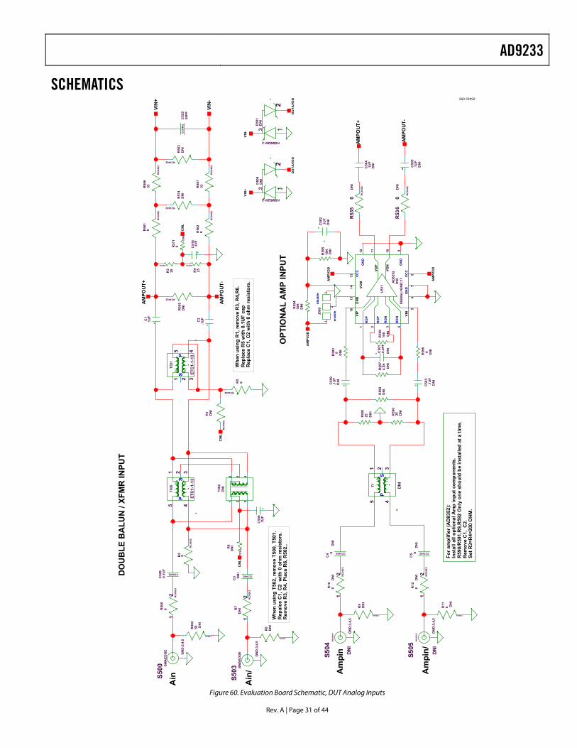
AD9233
Rev. A | Page 31 of 44
SCHEMATICS
DN
I
RC0603
RC
0603
RC
0603
CC0402
SMA
EDG
E
SMA
EDG
E
CC
0402
CC0402
ETC
1-1-
13
SP
RC
0402
RC
0402
RC0402
RC0402RC040 2
RC
0402
RC
0402
RC
0402
RC0402
RC
0402
RC
0402
RC0402
RC0402
RC0603
RC
0402
ETC
1-1-
13SP
SP
SMA
200U
P
SMA
200U
P
R59
0/R
591,
R9,
R59
2 O
nly
one
shou
ld b
e in
stal
led
at a
tim
e.
DO
UB
LE B
ALU
N /
XFM
R IN
PUT
DN
I
DN
I
DN
I
DN
I
DN
I
DN
ID
NI
DN
I
DN
I
DN
I
Whe
n us
ing
R1,
rem
ove
R3,
R4,
R6.
Rep
lace
C1,
C2
with
0 o
hm re
sist
ors.
For a
mpl
ifier
(AD
8352
):
Whe
n us
ing
T502
, rem
ove
T500
, T50
1.R
epal
ce C
1, C
2 w
ith 0
ohm
resi
stor
s.O
PTIO
NA
L A
MP
INPU
T
Ain
Ain
/ Am
pin
Am
pin/
GN
D;3
,4,5
S505
DN
I
S504
GN
D;3
,4,5
DN
I
5 4321
T1 DN
I
1 2 345
T500
50R50
2
DN
IR
1
R8
DN
I
912
67
15
41 32
813
51614
1011
U51
1
SIG
NA
L=G
ND
;17
R53
60
R59
32
31
J500
R59
410
K
R59
510
K
0R5
R56
3D
NI
R56
633 33R
567
R57
4D
NI
0R56
2
R56
10
0R57
125R
3 R4 25
DN
IR
565
0R2
DN
IR6
4.3K
R59
7
R59
02525R59
1
R59
2
R59
6
R59
810
0
21 3
5 4
T501
13
2
D50
1
HSMS2812
DN
I
13
2
D50
0
HSMS2812
DN
I
1 346
25
T502
CM
L
.1U
FC
510
CM
L
0.3P
FC
501
C50
9.1
UF
C50
3.1
UF
0.1U
FC
528
VIN
+
DU
TAVD
D
VIN
-
VIN
+.1
UF
C1
.1U
FC
2
.1U
FC
500
20P
FC
529
C50
5.1
UF
.1U
FC
504
.1U
FC
502
VIN
-
DU
TAVD
D
AM
POU
T+
AM
POU
T-
CM
L
AM
PVD
D
AM
PVD
D
AM
PVD
D
AM
POU
T+
AM
POU
T-
0R
535
GN
D;3
,4,5
S500
S503
GN
D;3
,4,5
C3 D
NI
12
DN
IR7
12
R56
00
21
R10
00
C4
DN
IR
9
12
0R12
C5 0
R11
0
DN
I
RC060 3
DN
I
Rem
ove
R3,
R4.
Pla
ce R
6, R
502,
.
RC
0603
DN
I
CC0402
DN
I
RC
0603
DN
I
CC0402
DN
I
RC060 3
DN
IIn
stal
l all
optio
nal A
mp
inpu
t com
pone
nts.
Rem
ove
C1,
C2.
Set R
3=R
4=20
0 O
HM
.
DN
I
Rep
lace
R5
with
0.1
UF
cap DN
I
enab
le
disa
ble
0
ENB
VCM
VIN
VIP
VO
N
VO
P
AD
8352
VCC
GN
D
GN
D
GN
D
VCC
RG
N
RD
N
RG
P
RD
P
DN
ID
NI
DN
I
0
RC
0402DN
I
RC
0402DN
I
05492-058
Figure 60. Evaluation Board Schematic, DUT Analog Inputs
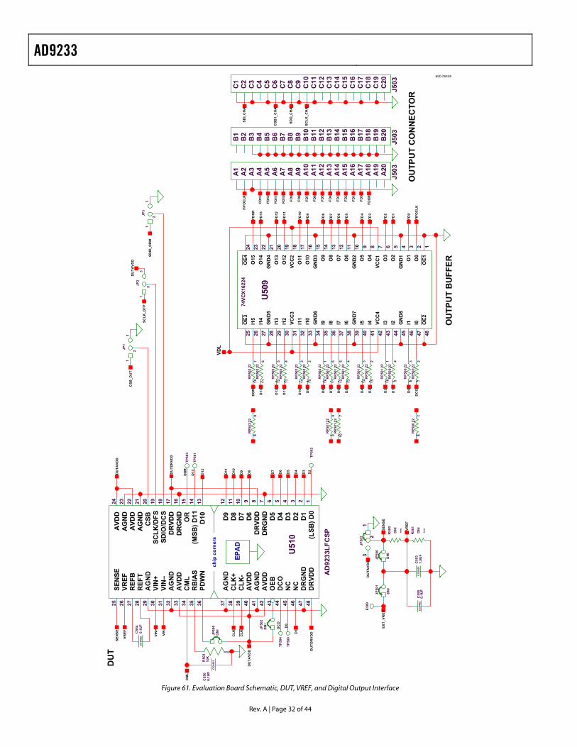
AD9233
Rev. A | Page 32 of 44
CC
0402
CC
0402
CC
0805
GN
D1
O2
O3
VCC
1O4
O5
GN
D2
O6
O7
O8
O9
GN
D3
O10
O11
VCC
2O
12O
13G
ND
4O
14O
15
I0I1GN
D8
I2I3VCC
4I4I5G
ND
7I6I7I8I9G
ND
6I1
0I1
1VC
C3
I12
I13
GN
D5
I14
I15
OE4
OE1O
0O
1
OE3
OE2
CC
0603
AD
9233
LFC
SP
D2
D3
VIN
–
CM
L
(LSB
) D0
D1
AG
ND
AVD
D
CLK
-A
VDD
AG
ND
AVD
D
D4
D5
DR
GN
DD
RVD
D
NC
D8
AVD
DSE
NSE
VREF
REF
B
D9
D10
DR
GN
DD
RVD
DSD
IO/D
CS
SCLK
/DFS
CSB
AG
ND
RB
IAS
OR
AG
ND
AG
ND
(MSB
) D11
AVD
D
VIN
+
D7
DC
O
D6
REF
T
CLK
+
PDW
N
NC
DR
GN
DD
RVD
D
AG
ND
OEB
EPA
D
chip
cor
ners
RC060 3
OU
TPU
T B
UFF
ER
OU
TPU
T C
ON
NEC
TOR
DU
T
B1
B2
B3
B4
B5
B6
B7
B8
B9
B10
B11
B12
B13
B14
B15
B16
B17
B18
B19
B20
J503
A1
A2
A3
A4
A5
A6
A7
A8
A9
A10
A11
A12
A13
A14
A15
A16
A17
A18
A19
A20
J503
710
22R
P501
98
RP5
0122
98
RP5
0222
81
22R
P500
710
22R
P502
611
22R
P502
512
22R
P502
413
22R
P502
314
22R
P502
215
22R
P502
116
22R
P502
611
22R
P501
512
22R
P501
413
22R
P501
314
22R
P501
215
22R
P501
116
22R
P501
45
RP5
0022
36
RP5
0022
27
RP5
0022
DN
IR
500
R04
02
DN
I
R50
1
R04
02
10K
R50
3
TP50
3
C1
C2
C3
C4
C5
C6
C7
C8
C9
C10
C11
C12
C13
C14
C15
C16
C17
C18
C19
C20
J503
13
2JP3
13
2JP2
13
2JP1
34
31 34
12
32 33 39 40 41 42
5678
45
112425 26 27
1213161718192021
351523
29
1422
30
10
44
9
28 3836 46 47 4837 43
U51
0
JP50
2D
NI
0.1U
FC
556
JP50
6D
NI
13
2
JP50
7
DU
TAVD
D
JP50
0
DN
I
JP50
1
DN
I
VRE
F
CSB
_DU
T
E50
0
ES
NE
SF
ER
V_TX
E
DU
TAVD
D
DU
TAVD
D
D12
TP50
1D
13
DO
R
DU
TDR
VDD TP
502
D2
DU
TDR
VDD
VRE
F
SEN
SE
VIN
-
VIN
+
D0
DC
O
SCLK
_CH
A
SDO
_CH
A
CSB
1_C
HA
SDI_
CH
AFI
FOC
LK
FD10
FD11
FD12
FD13
D1
FIFO
CLK
FD0
FD1
FD2
FD3
FD4
FD5
FD6
FD7
FD8
FD9
FD10
FD11
FD12
FD13
FDO
R
4567891011121314151617181920212223
4746454443424140393837363534333231302928272624 123
25 48
U50
9
74VC
X162
24
D3
D4
D5
D6
D7
D8
D9
D10
D11
TP50
0
TP50
4
1.0U
FC
553
DU
TAVD
D
CLK
CLK
D1
D9
DO
R
D13
D12
D11
D10 D
8
D7
D6
D5
D4
D3
D2
D0
DC
O
VDL
FD8
FDO
R
FD0
FD1
FD2
FD4
FD5
FD6
FD7
FD9
FD3
CM
L
SCLK
_DTP
SDIO
_OD
M
0.1U
FC
554
0.1U
FC
555
05492-059
Figure 61. Evaluation Board Schematic, DUT, VREF, and Digital Output Interface
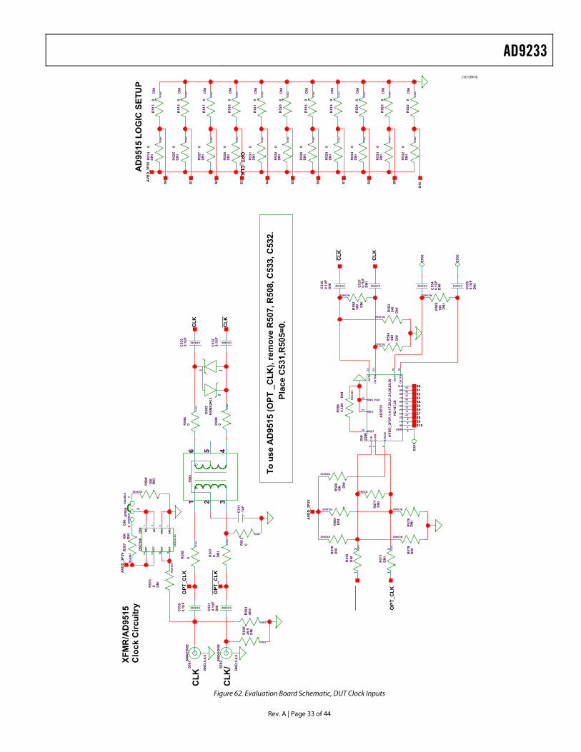
AD9233
Rev. A | Page 33 of 44
SMA
EDG
E
SMA
EDG
E
RC
0603
RC
0603
RC
0603
RC
0603
RC
0603
RC
0603
RC
0603
RC
0603
CC0402 CC0402
RC0402
RC0402
RC0402
CC0402 CC0402 CC0402
RC0402
RC0402
RC
0402
CC0402
RC060 3
RC
0603
RC
0603
CC0402
RC060 3
RC060 3
RC
0603
CC0402
RC
0603
RC
0603
RC
0603
RC
0603
RC
0603
RC
0603
Plac
e C
531,
R50
5=0.
CLK
/
CLK
XFM
R/A
D95
15C
lock
Circ
uitr
yA
D95
15 L
OG
IC S
ETU
P
21
DN
IR
511
21
DN
IR
510
OPT
_CLK
CLK
0R50
7
DN
I
0R50
8
AVD
D_3
P3V
S9
2 3 5
67891011121314151625
18192223
31
32
33
U50
0
AV
DD
_3P
3V;1
,4,1
7,20
,21,
24,2
6,29
,30
AVD
D_3
P3V
AVD
D_3
P3V
CLK
OPT
_CLK
CLK
S1
31
2
JP50
8
S8
S7
S6
S5S4S3S2
R51
40
DN
I
E50
1
R52
20
R52
30
R52
40
R51
90
R51
80
R52
00
R52
10
R51
60
R51
30
R51
50
R51
70
R52
60
DN
I
240
R58
3
0.1U
FC
537
DN
I
240
R58
4
0R50
913
2
D50
2H
SM
S28
12
49.9
R50
5
DN
I49
.9R
5040.1U
FC
531
DN
I
10K
R58
8
R52
50
DN
I
0R50
6
1 2 3456
T503
0R51
2
0.1U
FC
530
100
R58
5
E502
0R57
5
DN
I
4.12
KR
586
R58
010
KR
581
DN
I
R57
6D
NI
0.1U
FC
535
DN
I
0.1U
FC
534
DN
I
0.1U
FC
536
DN
I
C51
1.1
UF
E503
100
R58
2
S9S10
R57
8D
NI
R57
9D
NI
DN
IR
577
0.1U
FC
532
0.1U
FC
533
S7S8
S5S6
S4S3
S1S2
S0
14 12 10
1 53 78
OS
C50
0
R52
70
DN
I
R53
10
DN
I
R53
00
DN
I
R52
90
DN
I
R52
80
DN
I
R53
40
DN
I
R53
30
DN
I
R53
20
DN
I
OPT
_CLK
S0
GN
D;3
,4,5
S502
GN
D;3
,4,5
S501
CLK
OPT_C
LK
To u
se A
D95
15 (O
PT _
CLK
), re
mov
e R
507,
R50
8, C
533,
C53
2.
10K
R58
7EN
AB
LED
ISA
BLE
RC
0402
DN
I
CB
3LV-
3C
VCC
OU
T
OE
GN
D
OE
GN
DO
UT
VCC
DN
I
DN
I
RC0402
DN
I
DN
I
RC0402
RC
0402
DN
I
NC
=27,
28
AD
9515
CLK
CLK
B
GN D
GND_PAD
OU
T0
OU
T0B
OU
T1
OU
T1B
RSET
S0S1
S10
S2S3S4S5S6S7S8S9
SYN
CB
VREF
DN
I
RC0402
DN
I
RC0402
DN
I
RC0402
DN
I
RC0402
DN
I
S10
RC
0603
RC
0603D
NI
DN
I
RC
0603D
NI
RC
0603D
NI
RC
0603D
NI
RC
0603D
NI
RC
0603D
NI
RC
0603D
NI
RC
0603D
NI
RC
0603D
NI
RC
0603D
NI
05492-057
Figure 62. Evaluation Board Schematic, DUT Clock Inputs
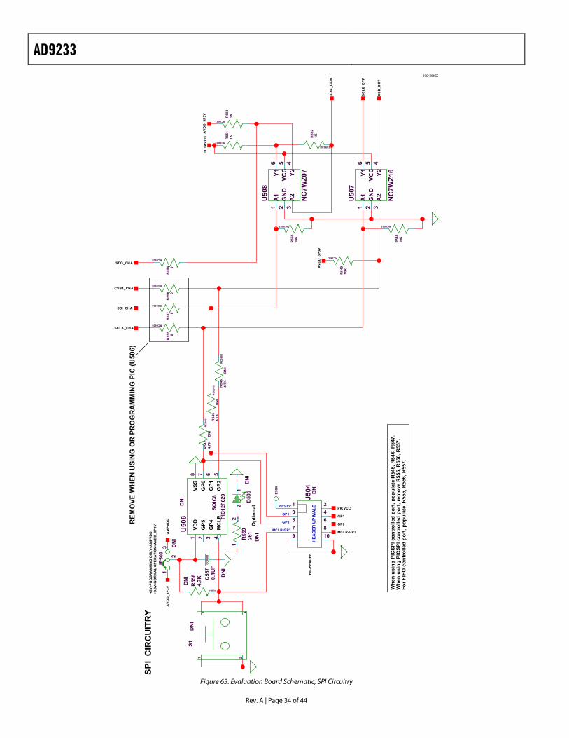
AD9233
Rev. A | Page 34 of 44
RC0603
RC0603
RC0603
RC
0603
RC
0603
RC0603
RC0603
RC0603
RC0603
RC0603
RC0603
RC0603
NC
7WZ0
7
A1
GN
DA
2
Y1VC
C Y2
NC
7WZ1
6
A1
GN
DA
2
Y1VC
C Y2
RC
0603
Opt
iona
l
+5V=
PRO
GR
AM
MIN
G O
NLY
=AM
PVD
DSP
I C
IRC
UIT
RY
GP0
PICVCC
GP1
For F
IFO
con
trol
led
port
, pop
ulat
e R
555,
R55
6, R
557.
Whe
n us
ing
PIC
SPI c
ontr
olle
d po
rt, p
opul
ate
R54
5, R
546,
R54
7.
REM
OVE
WH
EN U
SIN
G O
R P
RO
GR
AM
MIN
G P
IC (U
506)
Whe
n us
ing
PIC
SPI c
ontr
olle
d po
rt, r
emov
e R
555,
R55
6, R
557.
MCLR-GP3
+3.3
V=N
OR
MA
L O
PER
ATI
ON
=AVD
D_3
P3V
1
10
23 45 67 89
J504
PIC
-HEA
DER
24
13
7 6 532
81 4
U50
6
R54
74.
7KD
NI
1 3256 4
U50
7
1 3256 4
U50
8
R54
810
K
R54
910
K
1KR55
2
SDIO
_OD
M
CSB
_DU
T
SCLK
_DTP
R55
31K
R55
11K
R55
010
K
13
2
JP50
9
AVD
D_3
P3V
R55
4 0
R54
64.
7KD
NI
4.7K
R54
5D
NI
C55
70.
1UF
12
R55
926
1
R55
84.
7K
21
D50
5 E504
R55
7 0R
556 0
R55
50
SDO_CHA
CSB1_CHA
SDI_CHA
SCLK_CHA
AVD
D_3
P3V
DU
TAVD
D
DN
ID
NI
S1
DN
I
DN
I
DN
I
DN
I
DN
IH
EAD
ER U
P M
ALE
RC
0603
CC
0603
RC0603
DD
VP
MA
V3P3_D
DV
A
DN
I
PICVCC
GP1
GP0
MCLR-GP3
SOIC
8
GP5
GP4
GP0
GP2
GP1
VSS
VDD
MC
LR PIC
12F6
29
05492-056
Figure 63. Evaluation Board Schematic, SPI Circuitry
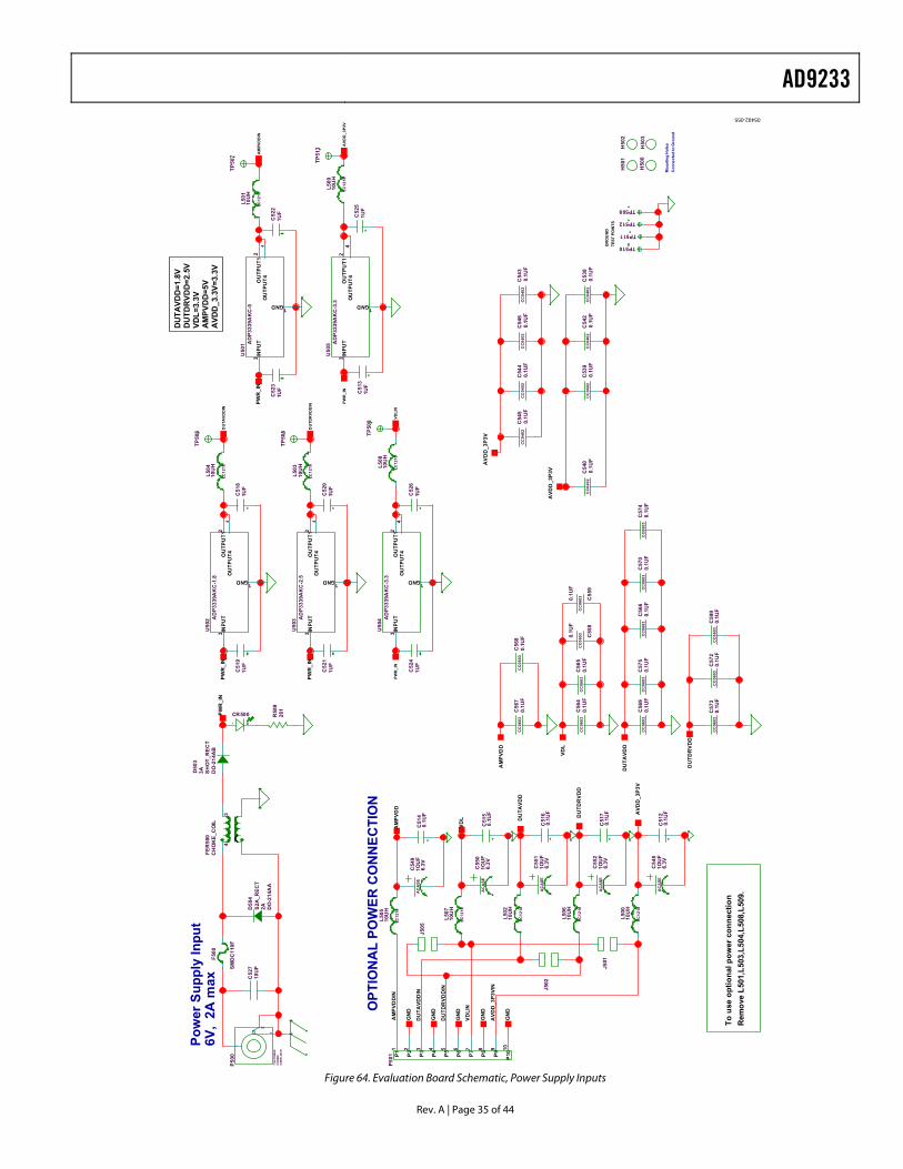
AD9233
Rev. A | Page 35 of 44
CC
0603
CC
0603
AC
ASE
LC12
10
CC
0603
CC
0603
CC
0603
AC
ASE
AC
ASE
AC
ASE
AC
ASE
CC
0603
CH
OK
E_C
OIL
DO
-214
AA
2AS2A
_REC
T
CC
0603
CC
0603
LC12
10
LC12
10
LC12
10
LC12
10
LC12
10
CC
0603
CC
0603
CC
0603
CC
0603
GND
1TU
PTU
OT
UPNI
OU
TPU
T4
LC12
10
LC12
10
CC
0402
CC
0402
CC
0402
CC
0402
CC
0402
CC
0402
CC
0402
CC
0402
LC12
10
GND
1TU
PTU
OT
UP
NIO
UTP
UT4
GND
1TU
PTU
OT
UP
NIO
UTP
UT4
LC12
10
GND
1TU
PTU
OT
UP
NIO
UTP
UT4
SMD
C11
0F
GND
1TU
PTU
OT
UPNI
OU
TPU
T4
P1
P2
P3
P4
P5
P6
P7
P8
P9
P10
CC
0603
CC
0603
Rem
ove
L501
,L50
3,L5
04,L
508,
L509
.To
use
opt
iona
l pow
er c
onne
ctio
n
OPT
ION
AL
POW
ER C
ON
NEC
TIO
N
Pow
er S
uppl
y In
put
6V,
2A m
axA
VDD
_3.3
V=3.
3V
Con
nect
ed to
Gro
und
Mou
ntin
g H
oles
DU
TDR
VDD
=2.5
VD
UTA
VDD
=1.8
V
VDL=
3.3V
GR
OU
ND
TEST
PO
INTS
AVD
D_3
P3V
AVD
D_3
P3V
J505
DU
TDR
VDD
IN J502
DU
TAVD
DIN
VD
LIN
AVD
D_3
P3V
AVD
D_3
P3V
AV
DD
_3P3
VIN
AM
PVD
DIN
TP51
3
DU
TDR
VDD
DU
TAVD
D
0.1U
FC
599
C57
20.
1UF
R58
926
1
C52
710
UF
21
CR500
J501
TP510
1 2 3 4 5 6 7 8 9 10
P501
1
23
4
U50
2 AD
P333
9AK
C-1
.8
H50
1
TP50
6
VDL
DU
TDR
VDD
F500
42
3
1
AD
P333
9AK
C-3
.3U
505
10U
HL5
09
1UF
C51
3
1
23
4
U50
1 AD
P333
9AK
C-5
1
23
4
U50
4 AD
P333
9AK
C-3
.3L5
0810
UH
H50
3
H50
2
TP512
TP511
H50
0
TP509
C52
61U
F
1UF
C52
5
TP50
8
C54
60.
1UF
C54
50.
1UF
C54
40.
1UF
C54
30.
1UF
C54
20.
1UF
C54
00.
1UF
C53
90.
1UF
C53
80.
1UF
L507
10U
H
L506
10U
H
1
23
4
U50
3 AD
P333
9AK
C-2
.5
0.1U
FC
575
0.1U
FC
574
0.1U
FC
573
0.1U
FC
570
L505
10U
H
L504
10U
H
L503
10U
H
L502
10U
H
L501
10U
H
0.1U
FC
569
0.1U
FC
568
D50
4
34
FER
500
1
2
3
P500
D50
3
SH
OT_
REC
T3A D
O-2
14A
B
0.1U
FC
567
C52
41U
F
C52
31U
FC
522
1UF
C52
11U
FC
520
1UF
C51
91U
FC
518
1UF
C51
70.
1UF
1OU
F6.
3V
C55
2
C51
60.
1UF
1OU
F6.
3V
C55
1
C51
50.
1UF
1OU
F6.
3V
C55
0
C51
40.
1UF
1OU
F6.
3V
C54
9
0.1U
FC
566
0.1U
FC
565
0.1U
FC
564
L500
10U
H
C51
20.
1UF
1OU
F6.
3V
C54
8
TP50
7
TP50
5
C55
9
0.1U
F0.
1UF
C55
8
GN
D
GN
D
AM
PVD
DIN
PWR
_IN
AM
PVD
D
VDL
AM
PVD
D
GN
D
GN
D
GN
D
VDLI
NPW
R_I
N
PWR
_IN
PWR
_IN
DU
TAVD
DIN
DU
TDR
VDD
INPWR
_IN
PWR
_IN
DU
TAVD
D
AM
PVD
D=5
V
CO
N00
57.
5V P
OW
ER
2.5M
M J
AC
K
05492-055
Figure 64. Evaluation Board Schematic, Power Supply Inputs
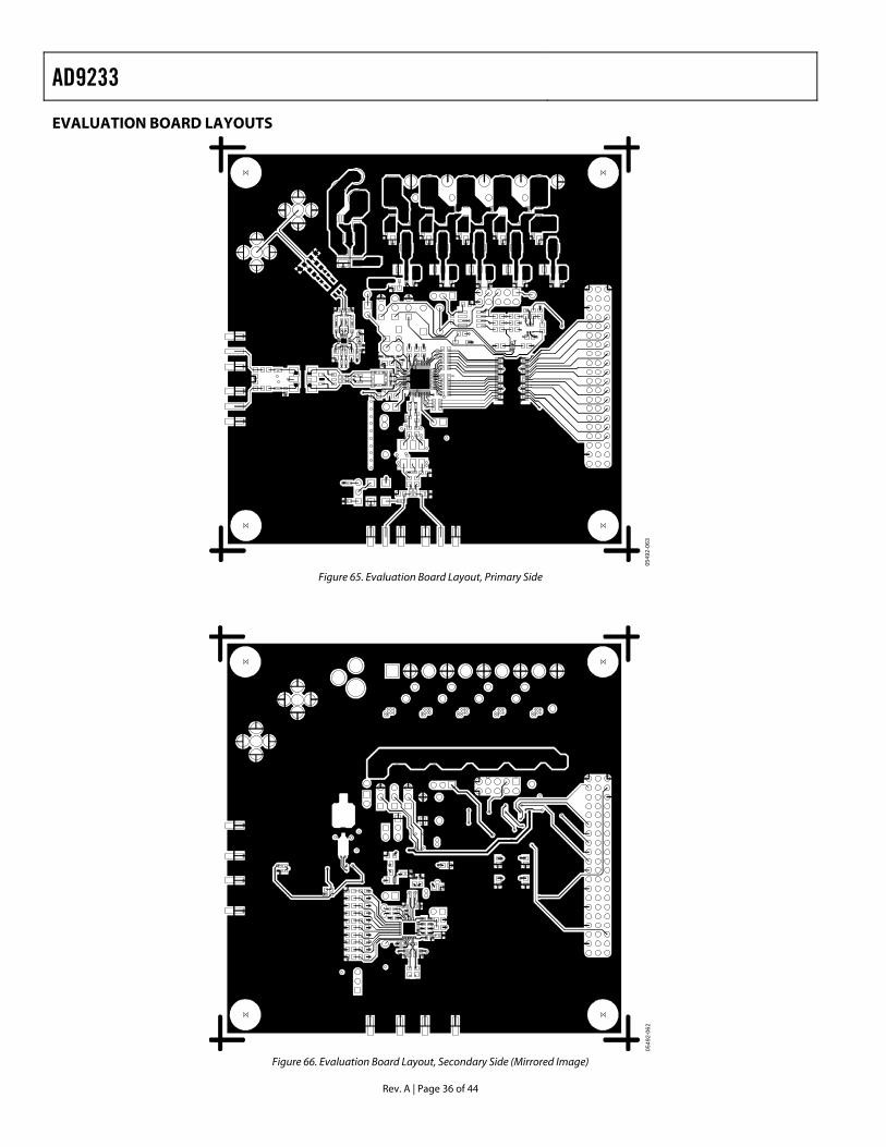
AD9233
Rev. A | Page 36 of 44
EVALUATION BOARD LAYOUTS
0549
2-06
3
Figure 65. Evaluation Board Layout, Primary Side
0549
2-06
2
Figure 66. Evaluation Board Layout, Secondary Side (Mirrored Image)
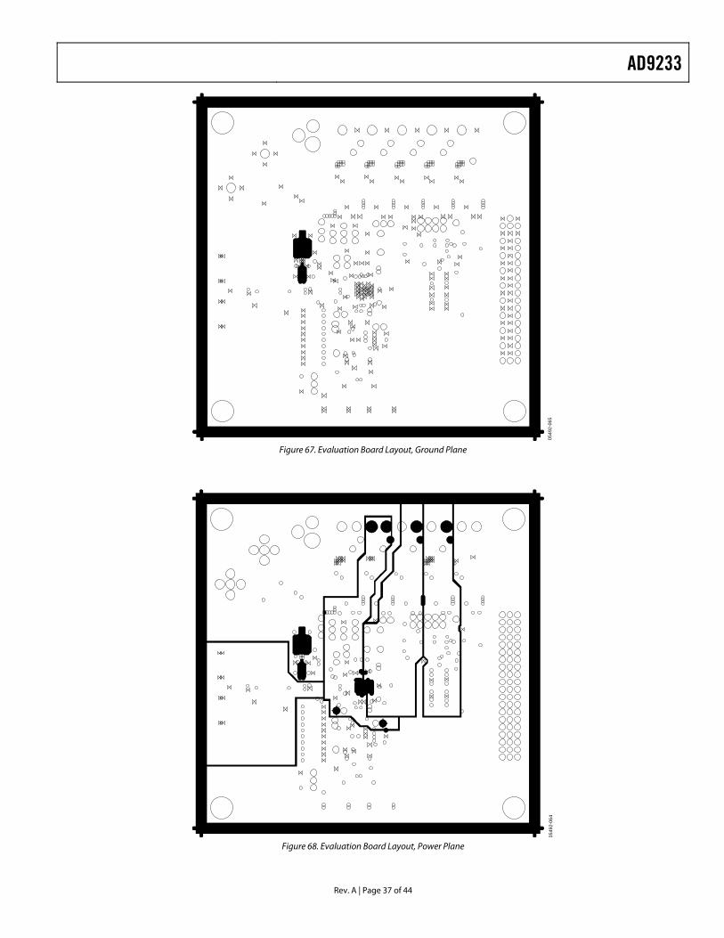
AD9233
Rev. A | Page 37 of 44
0549
2-06
5
Figure 67. Evaluation Board Layout, Ground Plane
0549
2-06
4
Figure 68. Evaluation Board Layout, Power Plane
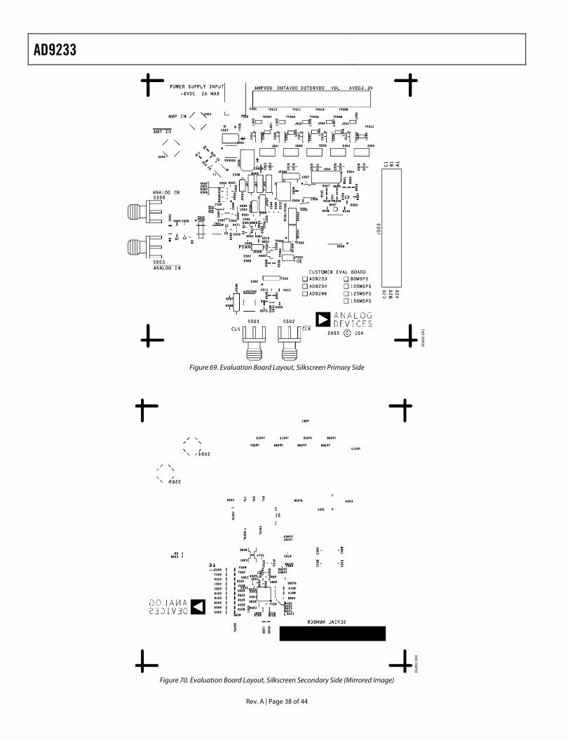
AD9233
Rev. A | Page 38 of 44
0549
2-06
1
Figure 69. Evaluation Board Layout, Silkscreen Primary Side
0549
2-06
0
Figure 70. Evaluation Board Layout, Silkscreen Secondary Side (Mirrored Image)
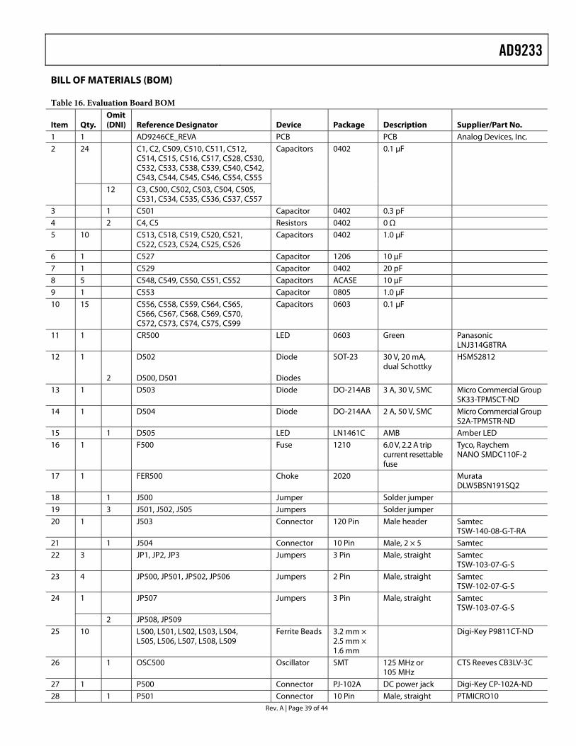
AD9233
Rev. A | Page 39 of 44
BILL OF MATERIALS (BOM) Table 16. Evaluation Board BOM
Item Qty. Omit (DNI) Reference Designator Device Package Description Supplier/Part No.
1 1 AD9246CE_REVA PCB PCB Analog Devices, Inc. 2 24 C1, C2, C509, C510, C511, C512,
C514, C515, C516, C517, C528, C530, C532, C533, C538, C539, C540, C542, C543, C544, C545, C546, C554, C555
Capacitors 0402 0.1 μF
12 C3, C500, C502, C503, C504, C505, C531, C534, C535, C536, C537, C557
3 1 C501 Capacitor 0402 0.3 pF 4 2 C4, C5 Resistors 0402 0 Ω 5 10 C513, C518, C519, C520, C521,
C522, C523, C524, C525, C526 Capacitors 0402 1.0 μF
6 1 C527 Capacitor 1206 10 μF 7 1 C529 Capacitor 0402 20 pF 8 5 C548, C549, C550, C551, C552 Capacitors ACASE 10 μF 9 1 C553 Capacitor 0805 1.0 μF 10 15 C556, C558, C559, C564, C565,
C566, C567, C568, C569, C570, C572, C573, C574, C575, C599
Capacitors 0603 0.1 μF
11 1 CR500 LED 0603 Green Panasonic LNJ314G8TRA
12 1 D502 Diode SOT-23 30 V, 20 mA, dual Schottky
HSMS2812
2 D500, D501 Diodes 13 1 D503 Diode DO-214AB 3 A, 30 V, SMC Micro Commercial Group
SK33-TPMSCT-ND 14 1 D504 Diode DO-214AA 2 A, 50 V, SMC Micro Commercial Group
S2A-TPMSTR-ND 15 1 D505 LED LN1461C AMB Amber LED 16 1 F500 Fuse 1210 6.0 V, 2.2 A trip
current resettable fuse
Tyco, Raychem NANO SMDC110F-2
17 1 FER500 Choke 2020 Murata DLW5BSN191SQ2
18 1 J500 Jumper Solder jumper 19 3 J501, J502, J505 Jumpers Solder jumper 20 1 J503 Connector 120 Pin Male header Samtec
TSW-140-08-G-T-RA 21 1 J504 Connector 10 Pin Male, 2 × 5 Samtec 22 3 JP1, JP2, JP3 Jumpers 3 Pin Male, straight Samtec
TSW-103-07-G-S 23 4 JP500, JP501, JP502, JP506 Jumpers 2 Pin Male, straight Samtec
TSW-102-07-G-S 24 1 JP507 Jumpers 3 Pin Male, straight Samtec
TSW-103-07-G-S 2 JP508, JP509 25 10 L500, L501, L502, L503, L504,
L505, L506, L507, L508, L509 Ferrite Beads 3.2 mm ×
2.5 mm × 1.6 mm
Digi-Key P9811CT-ND
26 1 OSC500 Oscillator SMT 125 MHz or 105 MHz
CTS Reeves CB3LV-3C
27 1 P500 Connector PJ-102A DC power jack Digi-Key CP-102A-ND 28 1 P501 Connector 10 Pin Male, straight PTMICRO10
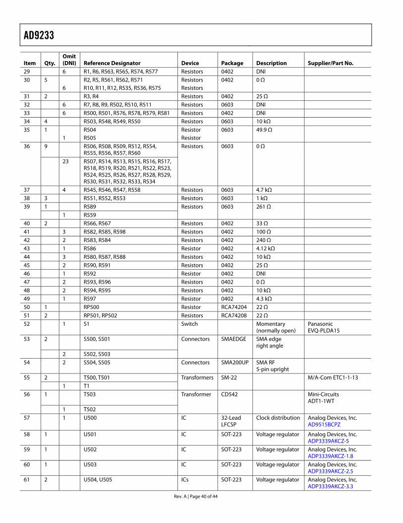
AD9233
Rev. A | Page 40 of 44
Item Qty. Omit (DNI) Reference Designator Device Package Description Supplier/Part No.
29 6 R1, R6, R563, R565, R574, R577 Resistors 0402 DNI 30 5 R2, R5, R561, R562, R571 Resistors 0402 0 Ω 6 R10, R11, R12, R535, R536, R575 Resistors 31 2 R3, R4 Resistors 0402 25 Ω 32 6 R7, R8, R9, R502, R510, R511 Resistors 0603 DNI 33 6 R500, R501, R576, R578, R579, R581 Resistors 0402 DNI 34 4 R503, R548, R549, R550 Resistors 0603 10 kΩ 35 1 R504 Resistor 0603 49.9 Ω 1 R505 Resistor 36 9 R506, R508, R509, R512, R554,
R555, R556, R557, R560 Resistors 0603 0 Ω
23 R507, R514, R513, R515, R516, R517, R518, R519, R520, R521, R522, R523, R524, R525, R526, R527, R528, R529, R530, R531, R532, R533, R534
37 4 R545, R546, R547, R558 Resistors 0603 4.7 kΩ 38 3 R551, R552, R553 Resistors 0603 1 kΩ 39 1 R589 Resistors 0603 261 Ω 1 R559 40 2 R566, R567 Resistors 0402 33 Ω 41 3 R582, R585, R598 Resistors 0402 100 Ω 42 2 R583, R584 Resistors 0402 240 Ω 43 1 R586 Resistor 0402 4.12 kΩ 44 3 R580, R587, R588 Resistors 0402 10 kΩ 45 2 R590, R591 Resistors 0402 25 Ω 46 1 R592 Resistor 0402 DNI 47 2 R593, R596 Resistors 0402 0 Ω 48 2 R594, R595 Resistors 0402 10 kΩ 49 1 R597 Resistor 0402 4.3 kΩ 50 1 RP500 Resistor RCA74204 22 Ω 51 2 RP501, RP502 Resistors RCA74208 22 Ω 52 1 S1 Switch Momentary
(normally open) Panasonic EVQ-PLDA15
53 2 S500, S501 Connectors SMAEDGE SMA edge right angle
2 S502, S503 54 2 S504, S505 Connectors SMA200UP SMA RF
5-pin upright
55 2 T500, T501 Transformers SM-22 M/A-Com ETC1-1-13 1 T1 56 1 T503 Transformer CD542 Mini-Circuits
ADT1-1WT 1 T502 57 1 U500 IC 32-Lead
LFCSP Clock distribution Analog Devices, Inc.
AD9515BCPZ
58 1 U501 IC SOT-223 Voltage regulator Analog Devices, Inc. ADP3339AKCZ-5
59 1 U502 IC SOT-223 Voltage regulator Analog Devices, Inc. ADP3339AKCZ-1.8
60 1 U503 IC SOT-223 Voltage regulator Analog Devices, Inc. ADP3339AKCZ-2.5
61 2 U504, U505 ICs SOT-223 Voltage regulator Analog Devices, Inc. ADP3339AKCZ-3.3
AD9233
Rev. A | Page 41 of 44
Item Qty. Omit (DNI) Reference Designator Device Package Description Supplier/Part No.
62 1 U506 IC 8-pin SOIC 8-bit microcontroller
Microchip PIC12F629
63 1 U507 IC SC70 Dual buffer Fairchild NC7WZ16 64 1 U508 IC SC70 Dual buffer Fairchild NC7WZ07 65 1 U509 IC 48-Lead
TSSOP Buffer/line driver Fairchild 74VCX162244
66 1 U510 DUT (AD9233)
48-Lead LFCSP
ADC Analog Devices, Inc. AD9233BCPZ
67 1 U511 (or Z500) IC 16-Lead LFCSP
Differential amplifier
Analog Devices, Inc. AD8352ACPZ
Total 128 107
AD9233
Rev. A | Page 42 of 44
OUTLINE DIMENSIONS
PIN 1INDICATOR
TOPVIEW
6.75BSC SQ
7.00BSC SQ
148
1213
3736
2425
4.254.10 SQ3.95
0.500.400.30
0.300.230.18
0.50 BSC
12° MAX
0.20 REF
0.80 MAX0.65 TYP
1.000.850.80
5.50REF
0.05 MAX0.02 NOM
0.60 MAX0.60 MAX PIN 1
INDICATOR
COPLANARITY0.08
SEATINGPLANE
0.25 MIN
EXPOSEDPAD
(BOTTOM VIEW)
COMPLIANT TO JEDEC STANDARDS MO-220-VKKD-2 Figure 71. 48-Lead Frame Chip Scale Package [LFCSP_VQ]
7 mm × 7 mm Body, Very Thin Quad (CP-48-3)
Dimensions shown in millimeters
ORDERING GUIDE Model Temperature Range Package Description Package Option1
AD9233BCPZ-1252 –40°C to +85°C 48-Lead Lead Frame Chip Scale Package [LFSCP_VQ] CP-48-3 AD9233BCPZRL7–1252 –40°C to +85°C 48-Lead Lead Frame Chip Scale Package [LFSCP_VQ] CP-48-3 AD9233BCPZ-1052 –40°C to +85°C 48-Lead Lead Frame Chip Scale Package [LFSCP_VQ] CP-48-3 AD9233BCPZRL7–1052 –40°C to +85°C 48-Lead Lead Frame Chip Scale Package [LFSCP_VQ] CP-48-3 AD9233BCPZ-802 –40°C to +85°C 48-Lead Lead Frame Chip Scale Package [LFSCP_VQ] CP-48-3 AD9233BCPZRL7–802 –40°C to +85°C 48-Lead Lead Frame Chip Scale Package [LFSCP_VQ] CP-48-3 AD9233-125EB Evaluation Board AD9233-105EB Evaluation Board AD9233-80EB Evaluation Board 1 It is required that the exposed paddle be soldered to the AGND plane to achieve the best electrical and thermal performance . 2 Z = Pb-free part.

AD9233
Rev. A | Page 43 of 44
NOTES

AD9233
Rev. A | Page 44 of 44
NOTES
©2006 Analog Devices, Inc. All rights reserved. Trademarks and registered trademarks are the property of their respective owners. D05492-0-8/06(A)