Embed Size (px)
Citation preview
14-Bit, 170 MSPS/210 MSPS/250 MSPS, 1.8 V Dual Analog-to-Digital Converter (ADC)
Data Sheet AD9643
Rev. E Document Feedback Information furnished by Analog Devices is believed to be accurate and reliable. However, no responsibility is assumed by Analog Devices for its use, nor for any infringements of patents or other rights of third parties that may result from its use. Specifications subject to change without notice. No license is granted by implication or otherwise under any patent or patent rights of Analog Devices. Trademarks and registered trademarks are the property of their respective owners.
One Technology Way, P.O. Box 9106, Norwood, MA 02062-9106, U.S.A. Tel: 781.329.4700 ©2011–2014 Analog Devices, Inc. All rights reserved. Technical Support www.analog.com
FEATURES SNR = 70.6 dBFS at 185 MHz AIN and 250 MSPS SFDR = 85 dBc at 185 MHz AIN and 250 MSPS −151.6 dBFS/Hz input noise at 185 MHz, −1 dBFS AIN and
250 MSPS Total power consumption: 785 mW at 250 MSPS 1.8 V supply voltages LVDS (ANSI-644 levels) outputs Integer 1-to-8 input clock divider (625 MHz maximum input) Sample rates of up to 250 MSPS IF sampling frequencies of up to 400 MHz Internal ADC voltage reference Flexible analog input range
1.4 V p-p to 2.0 V p-p (1.75 V p-p nominal) ADC clock duty cycle stabilizer 95 dB channel isolation/crosstalk Serial port control Energy saving power-down modes
APPLICATIONS Communications Diversity radio systems Multimode digital receivers (3G)
TD-SCDMA, WiMax, WCDMA, CDMA2000, GSM, EDGE, LTE I/Q demodulation systems Smart antenna systems General-purpose software radios Ultrasound equipment Broadband data applications
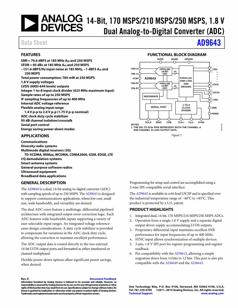
FUNCTIONAL BLOCK DIAGRAM
14
14
REFERENCE
SERIAL PORT
SCLK SDIO CSB CLK+ CLK– SYNC
1 TO 8CLOCKDIVIDER
AD9643
VIN+A D0±
D13±
DCO±
OR±
PDWN
OEB
VIN–A
VIN+B
VCM
VIN–B
NOTES1. THE D0± TO D13± PINS REPRESENT BOTH THE CHANNEL A
AND CHANNEL B LVDS OUTPUT DATA.
AVDD AGND DRVDD
0963
6-00
1
.....PARALLELDDR LVDS
ANDDRIVERS
PIPELINE14-BITADC
PIPELINE14-BITADC
Figure 1.
GENERAL DESCRIPTION The AD9643 is a dual, 14-bit analog-to-digital converter (ADC) with sampling speeds of up to 250 MSPS. The AD9643 is designed to support communications applications, where low cost, small size, wide bandwidth, and versatility are desired.
The dual ADC cores feature a multistage, differential pipelined architecture with integrated output error correction logic. Each ADC features wide bandwidth inputs supporting a variety of user-selectable input ranges. An integrated voltage reference eases design considerations. A duty cycle stabilizer is provided to compensate for variations in the ADC clock duty cycle, allowing the converters to maintain excellent performance.
The ADC output data is routed directly to the two external 14-bit LVDS output ports and formatted as either interleaved or channel multiplexed.
Flexible power-down options allow significant power savings, when desired.
Programming for setup and control are accomplished using a 3-wire SPI-compatible serial interface.
The AD9643 is available in a 64-lead LFCSP and is specified over the industrial temperature range of −40°C to +85°C. This product is protected by a U.S. patent.
PRODUCT HIGHLIGHTS 1. Integrated dual, 14-bit, 170 MSPS/210 MSPS/250 MSPS ADCs. 2. Operation from a single 1.8 V supply and a separate digital
output driver supply accommodating LVDS outputs. 3. Proprietary differential input maintains excellent SNR
performance for input frequencies of up to 400 MHz. 4. SYNC input allows synchronization of multiple devices. 5. 3-pin, 1.8 V SPI port for register programming and register
readback. 6. Pin compatibility with the AD9613, allowing a simple
migration down from 14 bits to 12 bits. This part is also pin compatible with the AD6649 and the AD6643.
AD9643 Data Sheet
Rev. E | Page 2 of 36
TABLE OF CONTENTS Features .............................................................................................. 1 Applications ....................................................................................... 1 Functional Block Diagram .............................................................. 1 General Description ......................................................................... 1 Product Highlights ........................................................................... 1 Revision History ............................................................................... 2 Specifications ..................................................................................... 3
ADC DC Specifications ............................................................... 3 ADC AC Specifications ............................................................... 4 Digital Specifications ................................................................... 6 Switching Specifications .............................................................. 8 Timing Specifications .................................................................. 9
Absolute Maximum Ratings .......................................................... 11 Thermal Characteristics ............................................................ 11 ESD Caution ................................................................................ 11
Pin Configurations and Function Descriptions ......................... 12 Typical Performance Characteristics ........................................... 16 Equivalent Circuits ......................................................................... 22 Theory of Operation ...................................................................... 23
ADC Architecture ...................................................................... 23
Analog Input Considerations ................................................... 23 Voltage Reference ....................................................................... 25 Clock Input Considerations ...................................................... 25 Power Dissipation and Standby Mode .................................... 26 Digital Outputs ........................................................................... 27 ADC Overrange (OR) ................................................................ 27
Channel/Chip Synchronization .................................................... 28 Serial Port Interface (SPI) .............................................................. 29
Configuration Using the SPI ..................................................... 29 Hardware Interface ..................................................................... 29 SPI Accessible Features .............................................................. 30
Memory Map .................................................................................. 31 Reading the Memory Map Register Table ............................... 31 Memory Map Register Table ..................................................... 32 Memory Map Register Description ......................................... 34
Applications Information .............................................................. 35 Design Guidelines ...................................................................... 35
Outline Dimensions ....................................................................... 36 Ordering Guide .......................................................................... 36
REVISION HISTORY 1/14—Rev. D to Rev. E
Changes to Figure 32 ...................................................................... 29
2/13—Rev. C to Rev. D
Added tSSYNC and tHSYNC Minimum Parameters of 1 ns, Table 5 .. 9
1/13—Rev. B to Rev. C
Changes to Features Section............................................................ 1 Changes to Input Referred Noise Parameter, Table 1 .................. 3 Changes to Table 2 ............................................................................ 4 Change to Table 3 ............................................................................. 6 Changes to Table 4 ............................................................................ 8 Changes to Figure 5 ........................................................................ 14 Changes to Figure 29 ...................................................................... 19 Changes to Figure 30 ...................................................................... 20 Change to Reading the Memory Map Register Table Section ....... 31 Changes to Table 14 ........................................................................ 33 Change to Memory Map Register Description Section............. 34 Updated Outline Dimensions ....................................................... 36
9/11—Rev. A to Rev. B
Changes to Table 1 ............................................................................. 3 Changes to Table 2, ........................................................................... 4 Changes to Table 3 ............................................................................. 6 Changes to Table 4 ............................................................................. 8 Changes to Table 8 .......................................................................... 12 Changes to Table 9 .......................................................................... 14 Changes to Typical Performance Characterisitics Section ....... 16 Added ADC Overrange (OR) Section ......................................... 27 Changes to Channel/Chip Synchronization Section ................. 28 Changes to Reading the Memory Map Register Table Section .............................................................................................. 31 Changes to Table 14 ....................................................................... 32 Changes to Memory Map Resgister Description Section ......... 34
5/11—Rev. 0 to Rev. A
Changes to Table 2, Worst Other (Harmonic or Spur) Max Values ......................................................................................... 4
4/11—Revision 0: Initial Version
Data Sheet AD9643
Rev. E | Page 3 of 36
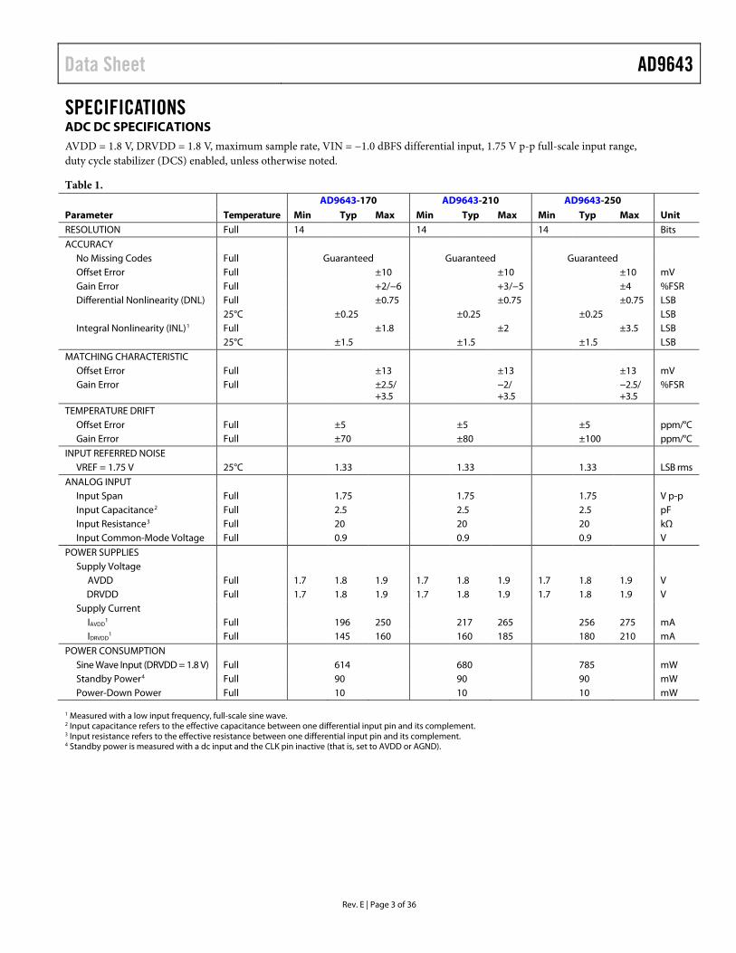
SPECIFICATIONS ADC DC SPECIFICATIONS AVDD = 1.8 V, DRVDD = 1.8 V, maximum sample rate, VIN = −1.0 dBFS differential input, 1.75 V p-p full-scale input range, duty cycle stabilizer (DCS) enabled, unless otherwise noted.
Table 1.
Parameter Temperature
AD9643-170 AD9643-210 AD9643-250
Min Typ Max Min Typ Max Min Typ Max Unit RESOLUTION Full 14 14 14 Bits
ACCURACY No Missing Codes Full Guaranteed Guaranteed Guaranteed Offset Error Full ±10 ±10 ±10 mV Gain Error Full +2/−6 +3/−5 ±4 %FSR Differential Nonlinearity (DNL) Full ±0.75 ±0.75 ±0.75 LSB 25°C ±0.25 ±0.25 ±0.25 LSB Integral Nonlinearity (INL)1 Full ±1.8 ±2 ±3.5 LSB 25°C ±1.5 ±1.5 ±1.5 LSB
MATCHING CHARACTERISTIC Offset Error Full ±13 ±13 ±13 mV Gain Error Full ±2.5/
+3.5 −2/
+3.5 −2.5/
+3.5 %FSR
TEMPERATURE DRIFT Offset Error Full ±5 ±5 ±5 ppm/°C Gain Error Full ±70 ±80 ±100 ppm/°C
INPUT REFERRED NOISE VREF = 1.75 V 25°C 1.33 1.33 1.33 LSB rms
ANALOG INPUT Input Span Full 1.75 1.75 1.75 V p-p Input Capacitance2 Full 2.5 2.5 2.5 pF Input Resistance3 Full 20 20 20 kΩ Input Common-Mode Voltage Full 0.9 0.9 0.9 V
POWER SUPPLIES Supply Voltage
AVDD Full 1.7 1.8 1.9 1.7 1.8 1.9 1.7 1.8 1.9 V DRVDD Full 1.7 1.8 1.9 1.7 1.8 1.9 1.7 1.8 1.9 V
Supply Current IAVDD
1 Full 196 250 217 265 256 275 mA IDRVDD
1 Full 145 160 160 185 180 210 mA
POWER CONSUMPTION Sine Wave Input (DRVDD = 1.8 V) Full 614 680 785 mW Standby Power4 Full 90 90 90 mW Power-Down Power Full 10 10 10 mW
1 Measured with a low input frequency, full-scale sine wave. 2 Input capacitance refers to the effective capacitance between one differential input pin and its complement. 3 Input resistance refers to the effective resistance between one differential input pin and its complement. 4 Standby power is measured with a dc input and the CLK pin inactive (that is, set to AVDD or AGND).
AD9643 Data Sheet
Rev. E | Page 4 of 36
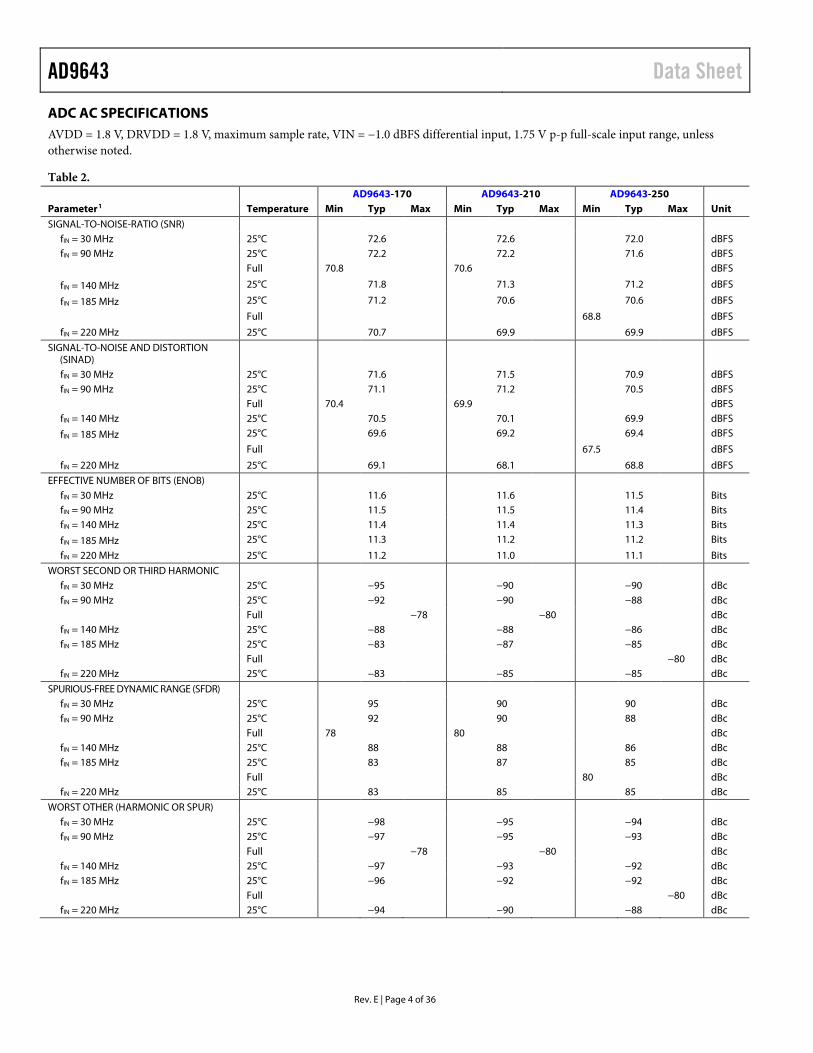
ADC AC SPECIFICATIONS AVDD = 1.8 V, DRVDD = 1.8 V, maximum sample rate, VIN = −1.0 dBFS differential input, 1.75 V p-p full-scale input range, unless otherwise noted.
Table 2. AD9643-170 AD9643-210 AD9643-250 Parameter1 Temperature Min Typ Max Min Typ Max Min Typ Max Unit
SIGNAL-TO-NOISE-RATIO (SNR) fIN = 30 MHz 25°C 72.6 72.6 72.0 dBFS fIN = 90 MHz 25°C 72.2 72.2 71.6 dBFS
Full 70.8 70.6 dBFS
fIN = 140 MHz 25°C 71.8 71.3 71.2 dBFS
fIN = 185 MHz 25°C 71.2 70.6 70.6 dBFS
Full 68.8 dBFS
fIN = 220 MHz 25°C 70.7 69.9 69.9 dBFS
SIGNAL-TO-NOISE AND DISTORTION (SINAD)
fIN = 30 MHz 25°C 71.6 71.5 70.9 dBFS fIN = 90 MHz 25°C 71.1 71.2 70.5 dBFS Full 70.4 69.9 dBFS fIN = 140 MHz 25°C 70.5 70.1 69.9 dBFS
fIN = 185 MHz 25°C 69.6 69.2 69.4 dBFS
Full 67.5 dBFS
fIN = 220 MHz 25°C 69.1 68.1 68.8 dBFS
EFFECTIVE NUMBER OF BITS (ENOB) fIN = 30 MHz 25°C 11.6 11.6 11.5 Bits fIN = 90 MHz 25°C 11.5 11.5 11.4 Bits fIN = 140 MHz 25°C 11.4 11.4 11.3 Bits
fIN = 185 MHz 25°C 11.3 11.2 11.2 Bits
fIN = 220 MHz 25°C 11.2 11.0 11.1 Bits
WORST SECOND OR THIRD HARMONIC fIN = 30 MHz 25°C −95 −90 −90 dBc fIN = 90 MHz 25°C −92 −90 −88 dBc Full −78 −80 dBc fIN = 140 MHz 25°C −88 −88 −86 dBc fIN = 185 MHz 25°C −83 −87 −85 dBc Full −80 dBc fIN = 220 MHz 25°C −83 −85 −85 dBc
SPURIOUS-FREE DYNAMIC RANGE (SFDR)
fIN = 30 MHz 25°C 95 90 90 dBc fIN = 90 MHz 25°C 92 90 88 dBc Full 78 80 dBc fIN = 140 MHz 25°C 88 88 86 dBc fIN = 185 MHz 25°C 83 87 85 dBc Full 80 dBc fIN = 220 MHz 25°C 83 85 85 dBc
WORST OTHER (HARMONIC OR SPUR) fIN = 30 MHz 25°C −98 −95 −94 dBc fIN = 90 MHz 25°C −97 −95 −93 dBc Full −78 −80 dBc fIN = 140 MHz 25°C −97 −93 −92 dBc fIN = 185 MHz 25°C −96 −92 −92 dBc Full −80 dBc fIN = 220 MHz 25°C −94 −90 −88 dBc
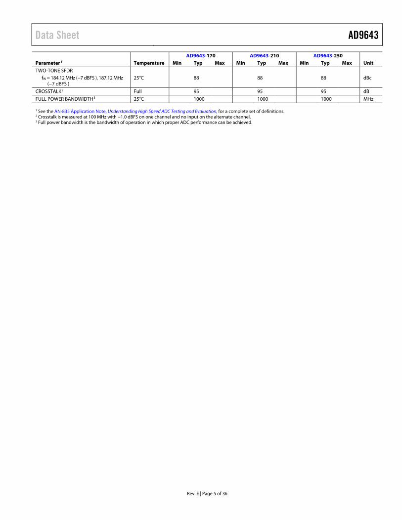
Data Sheet AD9643
Rev. E | Page 5 of 36
AD9643-170 AD9643-210 AD9643-250 Parameter1 Temperature Min Typ Max Min Typ Max Min Typ Max Unit
TWO-TONE SFDR
fIN = 184.12 MHz (−7 dBFS ), 187.12 MHz (−7 dBFS )
25°C 88 88 88 dBc
CROSSTALK2 Full 95 95 95 dB
FULL POWER BANDWIDTH3 25°C 1000 1000 1000 MHz 1 See the AN-835 Application Note, Understanding High Speed ADC Testing and Evaluation, for a complete set of definitions. 2 Crosstalk is measured at 100 MHz with −1.0 dBFS on one channel and no input on the alternate channel. 3 Full power bandwidth is the bandwidth of operation in which proper ADC performance can be achieved.
AD9643 Data Sheet
Rev. E | Page 6 of 36
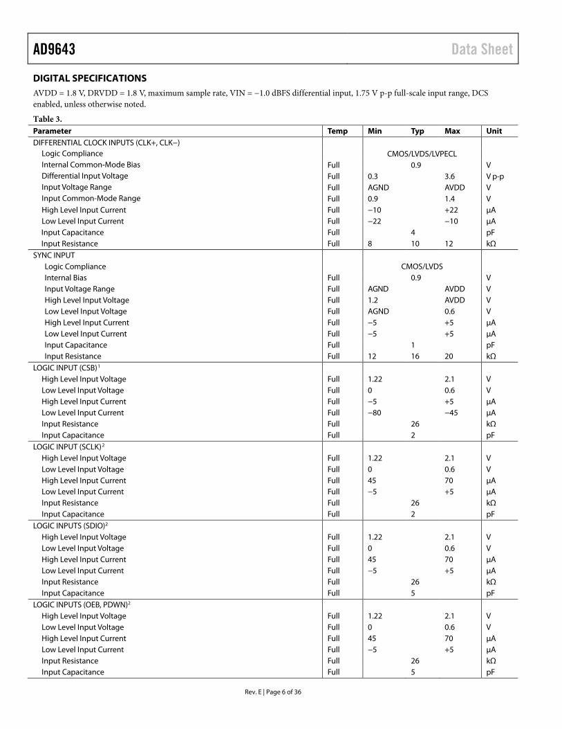
DIGITAL SPECIFICATIONS AVDD = 1.8 V, DRVDD = 1.8 V, maximum sample rate, VIN = −1.0 dBFS differential input, 1.75 V p-p full-scale input range, DCS enabled, unless otherwise noted.
Table 3. Parameter Temp Min Typ Max Unit DIFFERENTIAL CLOCK INPUTS (CLK+, CLK−)
Logic Compliance CMOS/LVDS/LVPECL Internal Common-Mode Bias Full 0.9 V Differential Input Voltage Full 0.3 3.6 V p-p Input Voltage Range Full AGND AVDD V Input Common-Mode Range Full 0.9 1.4 V High Level Input Current Full −10 +22 µA Low Level Input Current Full −22 −10 µA Input Capacitance Full 4 pF Input Resistance Full 8 10 12 kΩ
SYNC INPUT Logic Compliance CMOS/LVDS Internal Bias Full 0.9 V Input Voltage Range Full AGND AVDD V High Level Input Voltage Full 1.2 AVDD V Low Level Input Voltage Full AGND 0.6 V High Level Input Current Full −5 +5 µA Low Level Input Current Full −5 +5 µA Input Capacitance Full 1 pF Input Resistance Full 12 16 20 kΩ
LOGIC INPUT (CSB)1 High Level Input Voltage Full 1.22 2.1 V Low Level Input Voltage Full 0 0.6 V High Level Input Current Full −5 +5 µA Low Level Input Current Full −80 −45 µA Input Resistance Full 26 kΩ Input Capacitance Full 2 pF
LOGIC INPUT (SCLK)2 High Level Input Voltage Full 1.22 2.1 V Low Level Input Voltage Full 0 0.6 V High Level Input Current Full 45 70 µA Low Level Input Current Full −5 +5 µA Input Resistance Full 26 kΩ Input Capacitance Full 2 pF
LOGIC INPUTS (SDIO)2 High Level Input Voltage Full 1.22 2.1 V Low Level Input Voltage Full 0 0.6 V High Level Input Current Full 45 70 µA Low Level Input Current Full −5 +5 µA Input Resistance Full 26 kΩ Input Capacitance Full 5 pF
LOGIC INPUTS (OEB, PDWN)2 High Level Input Voltage Full 1.22 2.1 V Low Level Input Voltage Full 0 0.6 V High Level Input Current Full 45 70 µA Low Level Input Current Full −5 +5 µA Input Resistance Full 26 kΩ Input Capacitance Full 5 pF
Data Sheet AD9643
Rev. E | Page 7 of 36
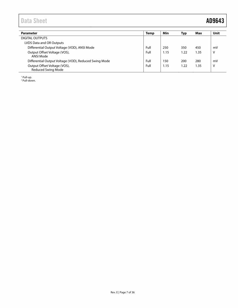
Parameter Temp Min Typ Max Unit DIGITAL OUTPUTS
LVDS Data and OR Outputs Differential Output Voltage (VOD), ANSI Mode Full 250 350 450 mV Output Offset Voltage (VOS),
ANSI Mode Full 1.15 1.22 1.35 V
Differential Output Voltage (VOD), Reduced Swing Mode Full 150 200 280 mV Output Offset Voltage (VOS),
Reduced Swing Mode Full 1.15 1.22 1.35 V
1 Pull-up. 2 Pull-down.
AD9643 Data Sheet
Rev. E | Page 8 of 36
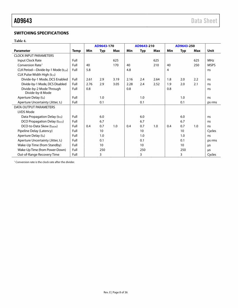
SWITCHING SPECIFICATIONS
Table 4. AD9643-170 AD9643-210 AD9643-250 Parameter Temp Min Typ Max Min Typ Max Min Typ Max Unit CLOCK INPUT PARAMETERS
Input Clock Rate Full 625 625 625 MHz Conversion Rate1 Full 40 170 40 210 40 250 MSPS CLK Period—Divide-by-1 Mode (tCLK) Full 5.8 4.8 4 ns CLK Pulse Width High (tCH)
Divide-by-1 Mode, DCS Enabled Full 2.61 2.9 3.19 2.16 2.4 2.64 1.8 2.0 2.2 ns Divide-by-1 Mode, DCS Disabled Full 2.76 2.9 3.05 2.28 2.4 2.52 1.9 2.0 2.1 ns Divide-by-2 Mode Through
Divide-by-8 Mode Full 0.8 0.8 0.8 ns
Aperture Delay (tA) Full 1.0 1.0 1.0 ns Aperture Uncertainty (Jitter, tJ) Full 0.1 0.1 0.1 ps rms
DATA OUTPUT PARAMETERS LVDS Mode
Data Propagation Delay (tPD) Full 6.0 6.0 6.0 ns DCO Propagation Delay (tDCO) Full 6.7 6.7 6.7 ns DCO-to-Data Skew (tSKEW) Full 0.4 0.7 1.0 0.4 0.7 1.0 0.4 0.7 1.0 ns
Pipeline Delay (Latency) Full 10 10 10 Cycles Aperture Delay (tA) Full 1.0 1.0 1.0 ns Aperture Uncertainty (Jitter, tJ) Full 0.1 0.1 0.1 ps rms Wake-Up Time (from Standby) Full 10 10 10 µs Wake-Up Time (from Power-Down) Full 250 250 250 µs Out-of-Range Recovery Time Full 3 3 3 Cycles
1 Conversion rate is the clock rate after the divider.
Data Sheet AD9643
Rev. E | Page 9 of 36
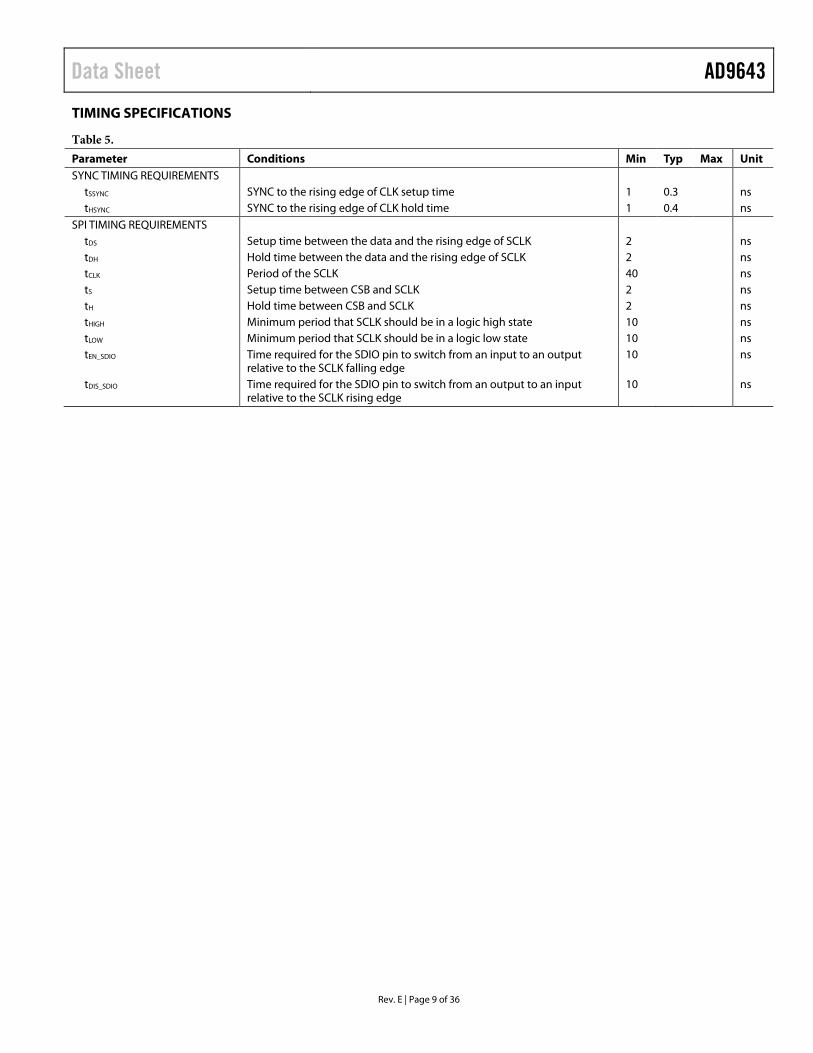
TIMING SPECIFICATIONS
Table 5. Parameter Conditions Min Typ Max Unit SYNC TIMING REQUIREMENTS
tSSYNC SYNC to the rising edge of CLK setup time 1 0.3 ns tHSYNC SYNC to the rising edge of CLK hold time 1 0.4 ns
SPI TIMING REQUIREMENTS tDS Setup time between the data and the rising edge of SCLK 2 ns tDH Hold time between the data and the rising edge of SCLK 2 ns tCLK Period of the SCLK 40 ns tS Setup time between CSB and SCLK 2 ns tH Hold time between CSB and SCLK 2 ns tHIGH Minimum period that SCLK should be in a logic high state 10 ns tLOW Minimum period that SCLK should be in a logic low state 10 ns tEN_SDIO Time required for the SDIO pin to switch from an input to an output
relative to the SCLK falling edge 10 ns
tDIS_SDIO Time required for the SDIO pin to switch from an output to an input relative to the SCLK rising edge
10 ns
AD9643 Data Sheet
Rev. E | Page 10 of 36
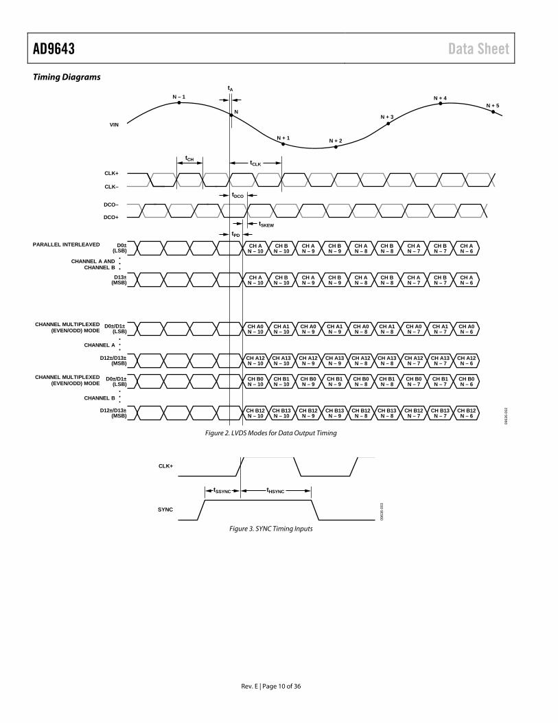
Timing Diagrams
VIN
CLK+
CLK–
DCO–
DCO+
D0±(LSB)
PARALLEL INTERLEAVED
CHANNEL MULTIPLEXED(EVEN/ODD) MODE
CHANNEL MULTIPLEXED(EVEN/ODD) MODE
D13±(MSB)
D0±/D1±(LSB)
CH AN – 10
CH BN – 10
CH AN – 9
CH BN – 9
CH AN – 8
CH BN – 8
CH AN – 7
CH BN – 7
CH AN – 6
CH AN – 10
CH BN – 10
CH AN – 9
CH BN – 9
CH AN – 8
CH BN – 8
CH AN – 7
CH BN – 7
CH AN – 6
CH A0N – 10
CH A1N – 10
CH A0N – 9
CH A1N – 9
CH A0N – 8
CH A1N – 8
CH A0N – 7
CH A1N – 7
CH A0N – 6
CH A12N – 10
CH A13N – 10
CH A12N – 9
CH A13N – 9
CH A12N – 8
CH A13N – 8
CH A12N – 7
CH A13N – 7
CH A12N – 6
CH B0N – 10
CH B1N – 10
CH B0N – 9
CH B1N – 9
CH B0N – 8
CH B1N – 8
CH B0N – 7
CH B1N – 7
CH B0N – 6
CH B12N – 10
CH B13N – 10
CH B12N – 9
CH B13N – 9
CH B12N – 8
CH B13N – 8
CH B12N – 7
CH B13N – 7
CH B12N – 6
CHANNEL A
D12±/D13±(MSB)
D0±/D1±(LSB)
CHANNEL B
D12±/D13±(MSB)
N – 1
N
N + 1 N + 2
N + 3
N + 4N + 5
tA
tCH
tPD
tSKEW
tDCO
tCLK
0963
6-00
2
...
...
...CHANNEL A AND
CHANNEL B
Figure 2. LVDS Modes for Data Output Timing
tSSYNC tHSYNC
SYNC
CLK+
0963
6-00
3
Figure 3. SYNC Timing Inputs
Data Sheet AD9643
Rev. E | Page 11 of 36
ABSOLUTE MAXIMUM RATINGS Table 6. Parameter Rating Electrical
AVDD to AGND −0.3 V to +2.0 V DRVDD to AGND −0.3 V to +2.0 V VIN+A/VIN+B, VIN−A/VIN−B to AGND −0.3 V to AVDD + 0.2 V CLK+, CLK− to AGND −0.3 V to AVDD + 0.2 V SYNC to AGND −0.3 V to AVDD + 0.2 V VCM to AGND −0.3 V to AVDD + 0.2 V CSB to AGND −0.3 V to DRVDD + 0.3 V SCLK to AGND −0.3 V to DRVDD + 0.3 V SDIO to AGND −0.3 V to DRVDD + 0.3 V OEB to AGND −0.3 V to DRVDD + 0.3 V PDWN to AGND −0.3 V to DRVDD + 0.3 V OR+/OR− to AGND −0.3 V to DRVDD + 0.3 V D0−/D0+ Through D13−/D13+
to AGND −0.3 V to DRVDD + 0.3 V
DCO+/DCO− to AGND −0.3 V to DRVDD + 0.3 V Environmental
Operating Temperature Range (Ambient)
−40°C to +85°C
Maximum Junction Temperature Under Bias
150°C
Storage Temperature Range (Ambient)
−65°C to +125°C
Stresses above those listed under Absolute Maximum Ratings may cause permanent damage to the device. This is a stress rating only; functional operation of the device at these or any other conditions above those indicated in the operational section of this specification is not implied. Exposure to absolute maximum rating conditions for extended periods may affect device reliability.
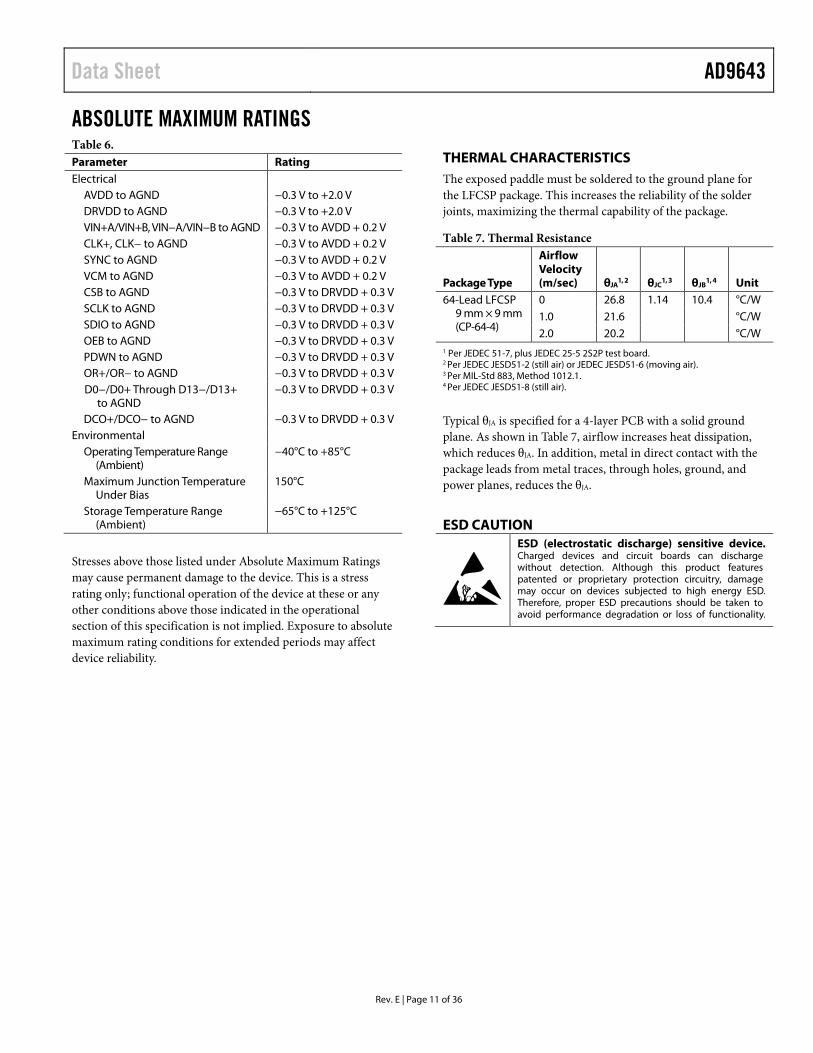
THERMAL CHARACTERISTICS The exposed paddle must be soldered to the ground plane for the LFCSP package. This increases the reliability of the solder joints, maximizing the thermal capability of the package.
Table 7. Thermal Resistance
Package Type
Airflow Velocity (m/sec) θJA
1, 2 θJC1, 3 θJB
1, 4 Unit 64-Lead LFCSP
9 mm × 9 mm (CP-64-4)
0 26.8 1.14 10.4 °C/W 1.0 21.6 °C/W 2.0 20.2 °C/W
1 Per JEDEC 51-7, plus JEDEC 25-5 2S2P test board. 2 Per JEDEC JESD51-2 (still air) or JEDEC JESD51-6 (moving air). 3 Per MIL-Std 883, Method 1012.1. 4 Per JEDEC JESD51-8 (still air).
Typical θJA is specified for a 4-layer PCB with a solid ground plane. As shown in Table 7, airflow increases heat dissipation, which reduces θJA. In addition, metal in direct contact with the package leads from metal traces, through holes, ground, and power planes, reduces the θJA.
ESD CAUTION
AD9643 Data Sheet
Rev. E | Page 12 of 36
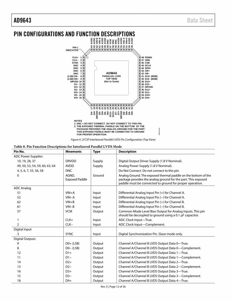
PIN CONFIGURATIONS AND FUNCTION DESCRIPTIONS
0963
6-00
4
17 18 19 20 21 22 23 24 25 26 27 28 29 30 31 32
D4–
D4+
DR
VDD
D5–
D5+ D6–
D6+
DC
O–
DC
O+
D7–
D7+
DR
VDD
D8–
D8+ D9–
D9+
64 63 62 61 60 59 58 57 56 55 54 53 52 51 50 49
AVD
DA
VDD
VIN
+BVI
N–B
AVD
DA
VDD
DN
CVC
MD
NC
DN
CA
VDD
AVD
DVI
N–A
VIN
+AA
VDD
AVD
D
123456789
10111213141516
CLK+CLK–SYNC
DNCDNCDNCDNC
(LSB) D0–(LSB) D0+
DRVDDD1–D1+D2–D2+D3–D3+
NOTES1. DNC = DO NOT CONNECT. DO NOT CONNECT TO THIS PIN.2. THE EXPOSED THERMAL PADDLE ON THE BOTTOM OF THE PACKAGE PROVIDES THE ANALOG GROUND FOR THE PART. THIS EXPOSED PADDLE MUST BE CONNECTED TO GROUND FOR PROPER OPERATION.
PDWNOEBCSBSCLKSDIOOR+OR–D13+ (MSB)D13– (MSB)D12+D12–DRVDDD11+D11–D10+D10–
48474645444342414039383736353433
AD9643PARALLEL LVDS
TOP VIEW(Not to Scale)
PIN 1INDICATOR
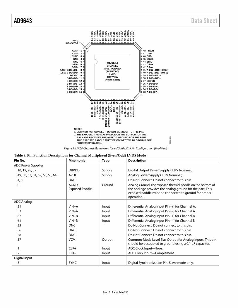
Figure 4. LFCSP Interleaved Parallel LVDS Pin Configuration (Top View)
Table 8. Pin Function Descriptions for Interleaved Parallel LVDS Mode Pin No. Mnemonic Type Description ADC Power Supplies
10, 19, 28, 37 DRVDD Supply Digital Output Driver Supply (1.8 V Nominal). 49, 50, 53, 54, 59, 60, 63, 64 AVDD Supply Analog Power Supply (1.8 V Nominal). 4, 5, 6, 7, 55, 56, 58 DNC Do Not Connect. Do not connect to this pin. 0 AGND,
Exposed Paddle Ground Analog Ground. The exposed thermal paddle on the bottom of the
package provides the analog ground for the part. This exposed paddle must be connected to ground for proper operation.
ADC Analog 51 VIN+A Input Differential Analog Input Pin (+) for Channel A. 52 VIN−A Input Differential Analog Input Pin (−) for Channel A. 62 VIN+B Input Differential Analog Input Pin (+) for Channel B. 61 VIN−B Input Differential Analog Input Pin (−) for Channel B. 57 VCM Output Common-Mode Level Bias Output for Analog Inputs. This pin
should be decoupled to ground using a 0.1 μF capacitor. 1 CLK+ Input ADC Clock Input—True. 2 CLK− Input ADC Clock Input—Complement.
Digital Input 3 SYNC Input Digital Synchronization Pin. Slave mode only.
Digital Outputs 9 D0+ (LSB) Output Channel A/Channel B LVDS Output Data 0—True. 8 D0− (LSB) Output Channel A/Channel B LVDS Output Data 0—Complement. 12 D1+ Output Channel A/Channel B LVDS Output Data 1—True. 11 D1− Output Channel A/Channel B LVDS Output Data 1—Complement. 14 D2+ Output Channel A/Channel B LVDS Output Data 2—True. 13 D2− Output Channel A/Channel B LVDS Output Data 2—Complement. 16 D3+ Output Channel A/Channel B LVDS Output Data 3—True. 15 D3− Output Channel A/Channel B LVDS Output Data 3—Complement. 18 D4+ Output Channel A/Channel B LVDS Output Data 4—True.
Data Sheet AD9643
Rev. E | Page 13 of 36
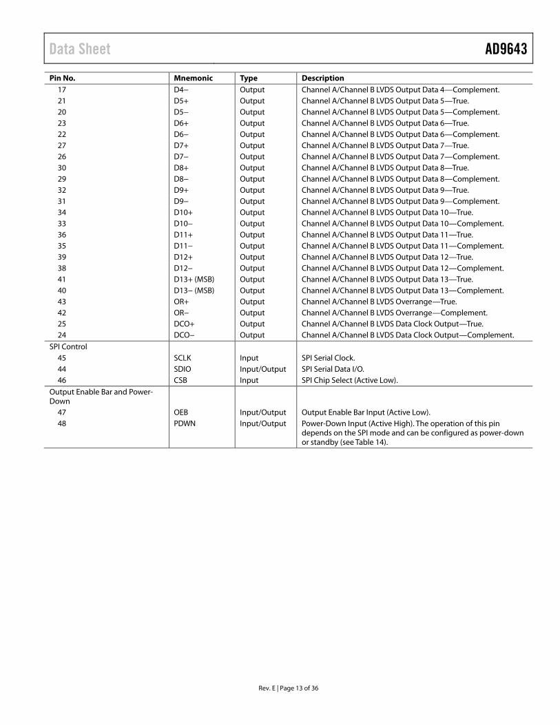
Pin No. Mnemonic Type Description 17 D4− Output Channel A/Channel B LVDS Output Data 4—Complement. 21 D5+ Output Channel A/Channel B LVDS Output Data 5—True. 20 D5− Output Channel A/Channel B LVDS Output Data 5—Complement. 23 D6+ Output Channel A/Channel B LVDS Output Data 6—True. 22 D6− Output Channel A/Channel B LVDS Output Data 6—Complement. 27 D7+ Output Channel A/Channel B LVDS Output Data 7—True. 26 D7− Output Channel A/Channel B LVDS Output Data 7—Complement. 30 D8+ Output Channel A/Channel B LVDS Output Data 8—True. 29 D8− Output Channel A/Channel B LVDS Output Data 8—Complement. 32 D9+ Output Channel A/Channel B LVDS Output Data 9—True. 31 D9− Output Channel A/Channel B LVDS Output Data 9—Complement. 34 D10+ Output Channel A/Channel B LVDS Output Data 10—True. 33 D10− Output Channel A/Channel B LVDS Output Data 10—Complement. 36 D11+ Output Channel A/Channel B LVDS Output Data 11—True. 35 D11− Output Channel A/Channel B LVDS Output Data 11—Complement. 39 D12+ Output Channel A/Channel B LVDS Output Data 12—True. 38 D12− Output Channel A/Channel B LVDS Output Data 12—Complement. 41 D13+ (MSB) Output Channel A/Channel B LVDS Output Data 13—True. 40 D13− (MSB) Output Channel A/Channel B LVDS Output Data 13—Complement. 43 OR+ Output Channel A/Channel B LVDS Overrange—True. 42 OR− Output Channel A/Channel B LVDS Overrange—Complement. 25 DCO+ Output Channel A/Channel B LVDS Data Clock Output—True. 24 DCO− Output Channel A/Channel B LVDS Data Clock Output—Complement.
SPI Control 45 SCLK Input SPI Serial Clock. 44 SDIO Input/Output SPI Serial Data I/O. 46 CSB Input SPI Chip Select (Active Low).
Output Enable Bar and Power-Down
47 OEB Input/Output Output Enable Bar Input (Active Low). 48 PDWN Input/Output Power-Down Input (Active High). The operation of this pin
depends on the SPI mode and can be configured as power-down or standby (see Table 14).
AD9643 Data Sheet
Rev. E | Page 14 of 36
0963
6-00
5
17 18 19 20 21 22 23 24 25 26 27 28 29 30 31 32
B D
8–/D
9–B
D8+
/D9+
DR
VDD
B D
10–/
D11
–B
D10
+/D
11+
(MSB
) B D
12–/
D13
–(M
SB) B
D12
+/D
13+
DC
O–
DC
O+
(LSB
) A D
0–/D
1–(L
SB) A
D0+
/D1+
DR
VDD
A D
2–/D
3–A
D2+
/D3+
A D
4–/D
5–A
D4+
/D5+
64 63 62 61 60 59 58 57 56 55 54 53 52 51 50 49
AVD
DA
VDD
VIN
+BVI
N–B
AVD
DA
VDD
DN
CVC
MD
NC
DN
CA
VDD
AVD
DVI
N–A
VIN
+AA
VDD
AVD
D
123456789
10111213141516
CLK+CLK–SYNC
DNCDNC
ORB–ORB+
(LSB) B D0–/D1–(LSB) B D0+/D1+
DRVDDB D2–/D3–B D2+/D3+B D4–/D5–B D4+/D5+B D6–/D7–B D6+/D7+
NOTES1. DNC = DO NOT CONNECT. DO NOT CONNECT TO THIS PIN.2. THE EXPOSED THERMAL PADDLE ON THE BOTTOM OF THE PACKAGE PROVIDES THE ANALOG GROUND FOR THE PART. THIS EXPOSED PADDLE MUST BE CONNECTED TO GROUND FOR PROPER OPERATION.
PDWNOEBCSBSCLKSDIOORA+ORA–A D12+/D13+ (MSB)A D12–/D13– (MSB)A D10+/D11+A D10–/D11–DRVDDA D8+/D9+A D8–/D9–A D6+/D7+A D6–/D7–
48474645444342414039383736353433
AD9643CHANNEL
MULTIPLEXED(EVEN/ODD)
LVDSTOP VIEW
(Not to Scale)
PIN 1INDICATOR
Figure 5. LFCSP Channel Multiplexed (Even/Odd) LVDS Pin Configuration (Top View)
Table 9. Pin Function Descriptions for Channel Multiplexed (Even/Odd) LVDS Mode Pin No. Mnemonic Type Description ADC Power Supplies
10, 19, 28, 37 DRVDD Supply Digital Output Driver Supply (1.8 V Nominal). 49, 50, 53, 54, 59, 60, 63, 64 AVDD Supply Analog Power Supply (1.8 V Nominal). 4, 5 DNC Do Not Connect. Do not connect to this pin. 0 AGND,
Exposed Paddle Ground Analog Ground. The exposed thermal paddle on the bottom of
the package provides the analog ground for the part. This exposed paddle must be connected to ground for proper operation.
ADC Analog 51 VIN+A Input Differential Analog Input Pin (+) for Channel A. 52 VIN−A Input Differential Analog Input Pin (−) for Channel A. 62 VIN+B Input Differential Analog Input Pin (+) for Channel B. 61 VIN−B Input Differential Analog Input Pin (−) for Channel B. 55 DNC Do Not Connect. Do not connect to this pin. 56 DNC Do Not Connect. Do not connect to this pin. 58 DNC Do Not Connect. Do not connect to this pin. 57 VCM Output Common-Mode Level Bias Output for Analog Inputs. This pin
should be decoupled to ground using a 0.1 μF capacitor. 1 CLK+ Input ADC Clock Input—True. 2 CLK− Input ADC Clock Input—Complement.
Digital Input 3 SYNC Input Digital Synchronization Pin. Slave mode only.
Data Sheet AD9643
Rev. E | Page 15 of 36
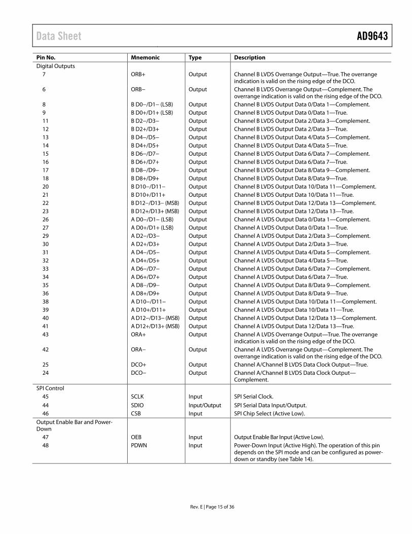
Pin No. Mnemonic Type Description Digital Outputs
7 ORB+ Output Channel B LVDS Overrange Output—True. The overrange indication is valid on the rising edge of the DCO.
6 ORB− Output Channel B LVDS Overrange Output—Complement. The overrange indication is valid on the rising edge of the DCO.
8 B D0−/D1− (LSB) Output Channel B LVDS Output Data 0/Data 1—Complement. 9 B D0+/D1+ (LSB) Output Channel B LVDS Output Data 0/Data 1—True. 11 B D2−/D3− Output Channel B LVDS Output Data 2/Data 3—Complement. 12 B D2+/D3+ Output Channel B LVDS Output Data 2/Data 3—True. 13 B D4−/D5− Output Channel B LVDS Output Data 4/Data 5—Complement. 14 B D4+/D5+ Output Channel B LVDS Output Data 4/Data 5—True. 15 B D6−/D7− Output Channel B LVDS Output Data 6/Data 7—Complement. 16 B D6+/D7+ Output Channel B LVDS Output Data 6/Data 7—True. 17 B D8−/D9− Output Channel B LVDS Output Data 8/Data 9—Complement. 18 B D8+/D9+ Output Channel B LVDS Output Data 8/Data 9—True. 20 B D10−/D11− Output Channel B LVDS Output Data 10/Data 11—Complement. 21 B D10+/D11+ Output Channel B LVDS Output Data 10/Data 11—True. 22 B D12−/D13− (MSB) Output Channel B LVDS Output Data 12/Data 13—Complement. 23 B D12+/D13+ (MSB) Output Channel B LVDS Output Data 12/Data 13—True. 26 A D0−/D1− (LSB) Output Channel A LVDS Output Data 0/Data 1—Complement. 27 A D0+/D1+ (LSB) Output Channel A LVDS Output Data 0/Data 1—True. 29 A D2−/D3− Output Channel A LVDS Output Data 2/Data 3—Complement. 30 A D2+/D3+ Output Channel A LVDS Output Data 2/Data 3—True. 31 A D4−/D5− Output Channel A LVDS Output Data 4/Data 5—Complement. 32 A D4+/D5+ Output Channel A LVDS Output Data 4/Data 5—True. 33 A D6−/D7− Output Channel A LVDS Output Data 6/Data 7—Complement. 34 A D6+/D7+ Output Channel A LVDS Output Data 6/Data 7—True. 35 A D8−/D9− Output Channel A LVDS Output Data 8/Data 9—Complement. 36 A D8+/D9+ Output Channel A LVDS Output Data 8/Data 9—True. 38 A D10−/D11− Output Channel A LVDS Output Data 10/Data 11—Complement. 39 A D10+/D11+ Output Channel A LVDS Output Data 10/Data 11—True. 40 A D12−/D13− (MSB) Output Channel A LVDS Output Data 12/Data 13—Complement. 41 A D12+/D13+ (MSB) Output Channel A LVDS Output Data 12/Data 13—True. 43 ORA+ Output Channel A LVDS Overrange Output—True. The overrange
indication is valid on the rising edge of the DCO. 42 ORA− Output Channel A LVDS Overrange Output—Complement. The
overrange indication is valid on the rising edge of the DCO. 25 DCO+ Output Channel A/Channel B LVDS Data Clock Output—True. 24 DCO− Output Channel A/Channel B LVDS Data Clock Output—
Complement. SPI Control
45 SCLK Input SPI Serial Clock.
44 SDIO Input/Output SPI Serial Data Input/Output. 46 CSB Input SPI Chip Select (Active Low).
Output Enable Bar and Power-Down
47 OEB Input Output Enable Bar Input (Active Low). 48 PDWN Input Power-Down Input (Active High). The operation of this pin
depends on the SPI mode and can be configured as power-down or standby (see Table 14).
AD9643 Data Sheet
Rev. E | Page 16 of 36
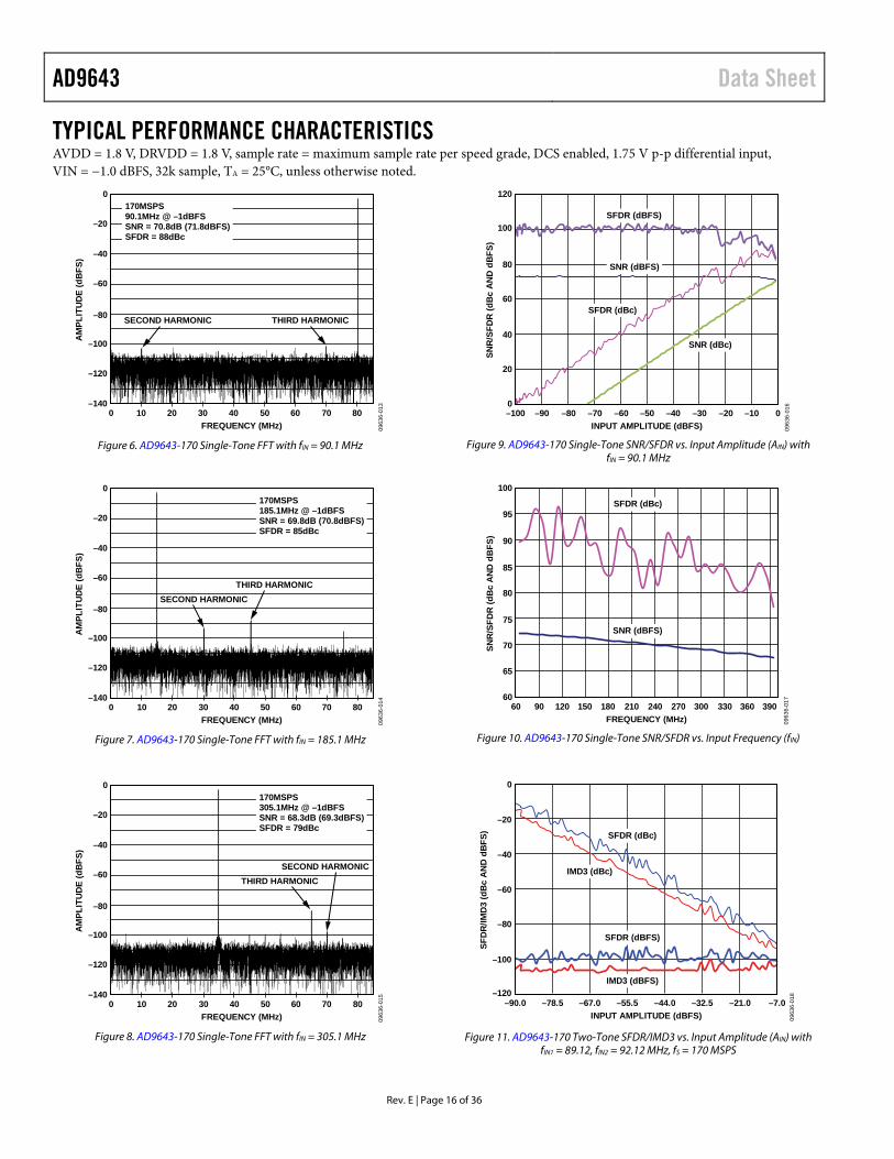
TYPICAL PERFORMANCE CHARACTERISTICS AVDD = 1.8 V, DRVDD = 1.8 V, sample rate = maximum sample rate per speed grade, DCS enabled, 1.75 V p-p differential input, VIN = −1.0 dBFS, 32k sample, TA = 25°C, unless otherwise noted.
0
–20
THIRD HARMONICSECOND HARMONIC
–40
–60
–80
–100
–120
–140100 20 30 40 50 60 70 80
FREQUENCY (MHz)
AM
PLIT
UD
E (d
BFS
)
0963
6-01
3
170MSPS90.1MHz @ –1dBFSSNR = 70.8dB (71.8dBFS)SFDR = 88dBc
Figure 6. AD9643-170 Single-Tone FFT with fIN = 90.1 MHz
0
–20
THIRD HARMONICSECOND HARMONIC
–40
–60
–80
–100
–120
–140100 20 30 40 50 60 70 80
FREQUENCY (MHz)
AM
PLIT
UD
E (d
BFS
)
0963
6-01
4
170MSPS185.1MHz @ –1dBFSSNR = 69.8dB (70.8dBFS)SFDR = 85dBc
Figure 7. AD9643-170 Single-Tone FFT with fIN = 185.1 MHz
0
–20
THIRD HARMONICSECOND HARMONIC
–40
–60
–80
–100
–120
–140100 20 30 40 50 60 70 80
FREQUENCY (MHz)
AM
PLIT
UD
E (d
BFS
)
0963
6-01
5
170MSPS305.1MHz @ –1dBFSSNR = 68.3dB (69.3dBFS)SFDR = 79dBc
Figure 8. AD9643-170 Single-Tone FFT with fIN = 305.1 MHz
120
100
80
60
40
20
0–10–20–30–40–50–60–70–80–90–100 0
INPUT AMPLITUDE (dBFS)
SNR
/SFD
R (d
Bc
AN
D d
BFS
)
0963
6-01
6
SFDR (dBFS)
SNR (dBFS)
SFDR (dBc)
SNR (dBc)
Figure 9. AD9643-170 Single-Tone SNR/SFDR vs. Input Amplitude (AIN) with
fIN = 90.1 MHz
100
95
90
85
80
75
70
65
60330 360 3903002702402101801501209060
FREQUENCY (MHz)
SNR
/SFD
R (d
Bc
AN
D d
BFS
)
0963
6-01
7
SNR (dBFS)
SFDR (dBc)
Figure 10. AD9643-170 Single-Tone SNR/SFDR vs. Input Frequency (fIN)
0
–20
–40
–60
–80
–100
–120–7.0–21.0–32.5–44.0–55.5–67.0–78.5–90.0
INPUT AMPLITUDE (dBFS)
SFD
R/IM
D3
(dB
c A
ND
dB
FS)
0963
6-01
8
SFDR (dBFS)
IMD3 (dBc)
IMD3 (dBFS)
SFDR (dBc)
Figure 11. AD9643-170 Two-Tone SFDR/IMD3 vs. Input Amplitude (AIN) with fIN1 = 89.12, fIN2 = 92.12 MHz, fS = 170 MSPS
Data Sheet AD9643
Rev. E | Page 17 of 36
0
–20
–40
–60
–80
–100
–120–7.0–21.0–32.5–44.0–55.5–67.0–78.5–90.0
INPUT AMPLITUDE (dBFS)
SFD
R/IM
D3
(dB
c A
ND
dB
FS)
0963
6-01
9
SFDR (dBFS)
IMD3 (dBc)
IMD3 (dBFS)
SFDR (dBc)
Figure 12. AD9643-170 Two-Tone SFDR/IMD3 vs. Input Amplitude (AIN) with fIN1 = 184.12, fIN2 = 187.12 MHz, fS = 170 MSPS
0
–20
–40
–60
–80
–100
–120
–140100 20 30 40 50 60 70 80
FREQUENCY (MHz)
AM
PLIT
UD
E (d
BFS
)
0963
6-02
0
170MSPS89.12MHz @ –7dBFS92.12MHz @ –7dBFSSFDR = 89dBc (96dBFS)
Figure 13. AD9643-170 Two-Tone FFT with fIN1 = 89.12, fIN2 = 92.12 MHz, fS = 170 MSPS
0
–20
–40
–60
–80
–100
–120
–140100 20 30 40 50 60 70 80
FREQUENCY (MHz)
AM
PLIT
UD
E (d
BFS
)
0963
6-02
1
170MSPS184.12MHz @ –7dBFS187.12MHz @ –7dBFSSFDR = 84dBc (91dBFS)
Figure 14. AD9643-170 Two-Tone FFT with fIN1 = 184.12, fIN2 = 187.12 MHz, fS = 170 MSPS
100
95
90
85
80
75
70130 140 150 160120110100908070605040 170
SAMPLE RATE (MSPS)
SNR
/SFD
R (d
Bc
AN
D d
BFS
)
0963
6-02
2
SFDR, CHANNEL BSNR, CHANNEL BSFDR, CHANNEL ASNR, CHANNEL A
Figure 15. AD9643-170 Single-Tone SNR/SFDR vs. Sample Rate (fS) with fIN = 90.1 MHz
6000
5000
4000
3000
2000
1000
0N + 2 N + 3 N + 4 N + 5N + 1NN – 1N – 2N – 3N – 4N – 5
OUTPUT CODE
NU
MB
ER O
F H
ITS
0963
6-02
3
1.34LSB rms16,379 TOTAL HITS
Figure 16. AD9643-170 Grounded Input Histogram
0
–20
THIRD HARMONIC
SECOND HARMONIC
–40
–60
–80
–100
–120
–140100 20 30 40 50 60 70 80 90 100
FREQUENCY (Hz)
AM
PLIT
UD
E (d
BFS
)
0963
6-02
4
210MSPS90.1MHz @ –1dBFSSNR = 70.6dB (71.6dBFS)SFDR = 88dBc
Figure 17. AD9643-210 Single-Tone FFT with fIN = 90.1 MHz
AD9643 Data Sheet
Rev. E | Page 18 of 36
THIRD HARMONICSECOND HARMONIC
0
–20
–40
–60
–80
–100
–120
–140100 20 30 40 50 60 70 80 90 100
FREQUENCY (MHz)
AM
PLIT
UD
E (d
BFS
)
0963
6-02
5
210MSPS185.1MHz @ –1dBFSSNR = 70.3dB (71.3dBFS)SFDR = 86dBc
Figure 18. AD9643-210 Single-Tone FFT with fIN = 185.1 MHz
0
–20
THIRD HARMONICSECOND HARMONIC
–40
–60
–80
–100
–120
–140100 20 30 40 50 60 70 80 90 100
FREQUENCY (MHz)
AM
PLIT
UD
E (d
BFS
)
0963
6-02
6
210MSPS305.1MHz @ –1dBFSSNR = 67.3dB (68.3dBFS)SFDR = 75dBc
Figure 19. AD9643-210 Single-Tone FFT with fIN = 305.1 MHz
120
100
80
60
40
20
0–10–20–30–40–50–60–70–80–90–100 0
INPUT AMPLITUDE (dBFS)
SNR
/SFD
R (d
Bc
AN
D d
BFS
)
0963
6-02
7
SFDR (dBFS)
SNR (dBFS)
SFDR (dBc)
SNR (dBc)
Figure 20. AD9643-210 Single-Tone SNR/SFDR vs. Input Amplitude (AIN)
with fIN = 90.1 MHz
100
95
90
85
80
75
70
65
60
SNR
/SFD
R (d
Bc
AN
D d
BFS
)
0963
6-02
8
330 360 3903002702402101801501209060FREQUENCY (MHz)
SNR (dBFS)
SFDR (dBc)
Figure 21. AD9643-210 Single-Tone SNR/SFDR vs. Input Frequency (fIN)
0
–20
–40
–60
–80
–100
–120–7.0–21.0–32.5–44.0–55.5–67.0–78.5–90.0
INPUT AMPLITUDE (dBFS)
SFD
R/IM
D3
(dB
c A
ND
dB
FS)
0963
6-02
9
SFDR (dBFS)
IMD3 (dBc)
IMD3 (dBFS)
SFDR (dBc)
Figure 22. AD9643-210 Two-Tone SFDR/IMD3 vs. Input Amplitude (AIN)
with fIN1 = 89.12, fIN2 = 92.12 MHz, fS = 210 MSPS
0
–20
–40
–60
–80
–100
–120–7.0–21.0–32.5–44.0–55.5–67.0–78.5–90.0
INPUT AMPLITUDE (dBFS)
SFD
R/IM
D3
(dB
c A
ND
dB
FS)
0963
6-03
0
SFDR (dBFS)
IMD3 (dBc)
IMD3 (dBFS)
SFDR (dBc)
Figure 23. AD9643-210 Two-Tone SFDR/IMD3 vs. Input Amplitude (AIN)
with fIN1 = 184.12, fIN2 = 187.12 MHz, fS = 210 MSPS
Data Sheet AD9643
Rev. E | Page 19 of 36
0
–20
–40
–60
–80
–100
–120
–140100 20 30 40 50 60 70 80 90 100
FREQUENCY (MHz)
AM
PLIT
UD
E (d
BFS
)
0963
6-03
1
210MSPS89.12MHz @ –7dBFS92.12MHz @ –7dBFSSFDR = 88dBc (95dBFS)
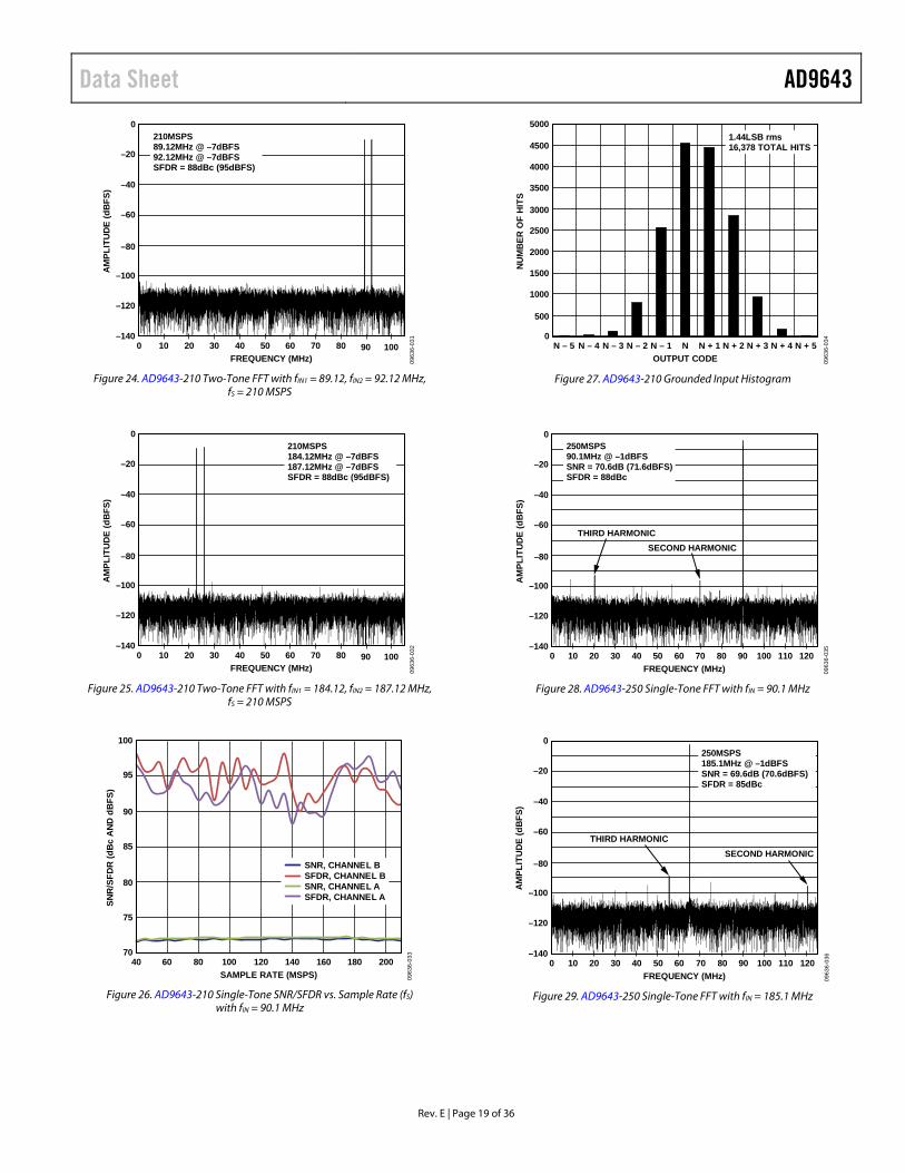
Figure 24. AD9643-210 Two-Tone FFT with fIN1 = 89.12, fIN2 = 92.12 MHz,
fS = 210 MSPS
0
–20
–40
–60
–80
–100
–120
–140100 20 30 40 50 60 70 80 90 100
FREQUENCY (MHz)
AM
PLIT
UD
E (d
BFS
)
0963
6-03
2
210MSPS184.12MHz @ –7dBFS187.12MHz @ –7dBFSSFDR = 88dBc (95dBFS)
Figure 25. AD9643-210 Two-Tone FFT with fIN1 = 184.12, fIN2 = 187.12 MHz,
fS = 210 MSPS
100
95
90
85
80
75
70140 160120100806040 180 200
SAMPLE RATE (MSPS)
SNR
/SFD
R (d
Bc
AN
D d
BFS
)
0963
6-03
3
SNR, CHANNEL BSFDR, CHANNEL BSNR, CHANNEL ASFDR, CHANNEL A
Figure 26. AD9643-210 Single-Tone SNR/SFDR vs. Sample Rate (fS)
with fIN = 90.1 MHz
5000
4500
4000
3500
3000
2500
2000
1500
1000
500
0N + 2 N + 3 N + 4 N + 5N + 1NN – 1N – 2N – 3N – 4N – 5
OUTPUT CODE
NU
MB
ER O
F H
ITS
0963
6-03
4
1.44LSB rms16,378 TOTAL HITS
Figure 27. AD9643-210 Grounded Input Histogram
0
–20
THIRD HARMONICSECOND HARMONIC
–40
–60
–80
–100
–120
–140100 20 30 40 50 60 70 80 90 100 110 120
FREQUENCY (MHz)
AM
PLIT
UD
E (d
BFS
)
0963
6-03
5
250MSPS90.1MHz @ –1dBFSSNR = 70.6dB (71.6dBFS)SFDR = 88dBc
Figure 28. AD9643-250 Single-Tone FFT with fIN = 90.1 MHz
0
–20
THIRD HARMONIC
–40
–60
–80
–100
–120
–140100 20 30 40 50 60 70 80 90 100 110 120
FREQUENCY (MHz)
AM
PLIT
UD
E (d
BFS
)
0963
6-03
6
250MSPS185.1MHz @ –1dBFSSNR = 69.6dB (70.6dBFS)SFDR = 85dBc
SECOND HARMONIC
Figure 29. AD9643-250 Single-Tone FFT with fIN = 185.1 MHz
AD9643 Data Sheet
Rev. E | Page 20 of 36
0
–20
THIRD HARMONICSECOND HARMONIC
–40
–60
–80
–100
–120
–140100 20 30 40 50 60 70 80 90 100 110 120
FREQUENCY (MHz)
AM
PLIT
UD
E (d
BFS
)
0963
6-03
7
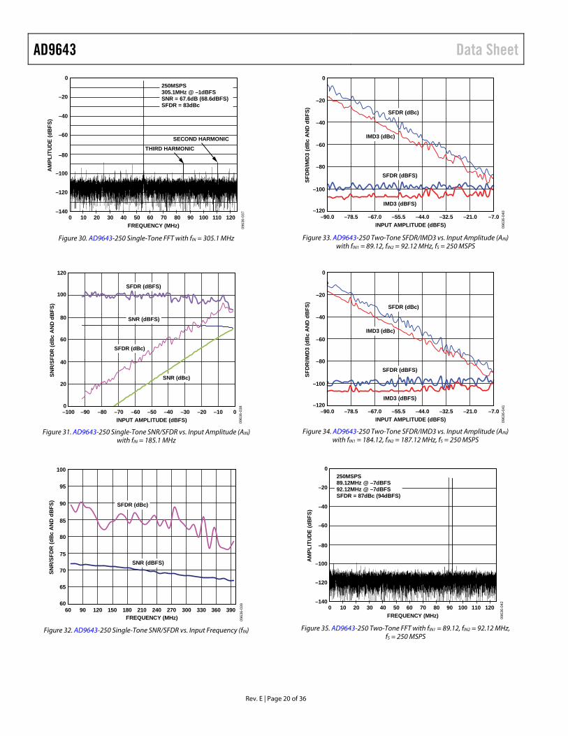
250MSPS305.1MHz @ –1dBFSSNR = 67.6dB (68.6dBFS)SFDR = 83dBc
Figure 30. AD9643-250 Single-Tone FFT with fIN = 305.1 MHz
120
100
80
60
40
20
0–10–20–30–40–50–60–70–80–90–100 0
INPUT AMPLITUDE (dBFS)
SNR
/SFD
R (d
Bc
AN
D d
BFS
)
0963
6-03
8
SFDR (dBFS)
SNR (dBFS)
SFDR (dBc)
SNR (dBc)
Figure 31. AD9643-250 Single-Tone SNR/SFDR vs. Input Amplitude (AIN)
with fIN = 185.1 MHz
100
95
90
85
80
75
70
65
60330 360 3903002702402101801501209060
FREQUENCY (MHz)
SNR
/SFD
R (d
Bc
AN
D d
BFS
)
0963
6-03
9
SNR (dBFS)
SFDR (dBc)
Figure 32. AD9643-250 Single-Tone SNR/SFDR vs. Input Frequency (fIN)
0
–20
–40
–60
–80
–100
–120–7.0–21.0–32.5–44.0–55.5–67.0–78.5–90.0
INPUT AMPLITUDE (dBFS)
SFD
R/IM
D3
(dB
c A
ND
dB
FS)
0963
6-04
0
SFDR (dBFS)
IMD3 (dBc)
IMD3 (dBFS)
SFDR (dBc)
Figure 33. AD9643-250 Two-Tone SFDR/IMD3 vs. Input Amplitude (AIN)
with fIN1 = 89.12, fIN2 = 92.12 MHz, fS = 250 MSPS
0
–20
–40
–60
–80
–100
–120–7.0–21.0–32.5–44.0–55.5–67.0–78.5–90.0
INPUT AMPLITUDE (dBFS)
SFD
R/IM
D3
(dB
c A
ND
dB
FS)
0963
6-04
1
SFDR (dBFS)
IMD3 (dBc)
IMD3 (dBFS)
SFDR (dBc)
Figure 34. AD9643-250 Two-Tone SFDR/IMD3 vs. Input Amplitude (AIN)
with fIN1 = 184.12, fIN2 = 187.12 MHz, fS = 250 MSPS
0
–20
–40
–60
–80
–100
–120
–140100 20 30 40 50 60 70 80 90 100 110 120
FREQUENCY (MHz)
AM
PLIT
UD
E (d
BFS
)
0963
6-04
2
250MSPS89.12MHz @ –7dBFS92.12MHz @ –7dBFSSFDR = 87dBc (94dBFS)
Figure 35. AD9643-250 Two-Tone FFT with fIN1 = 89.12, fIN2 = 92.12 MHz,
fS = 250 MSPS
Data Sheet AD9643
Rev. E | Page 21 of 36
0
–20
–40
–60
–80
–100
–120
–140100 20 30 40 50 60 70 80 90 100 110 120
FREQUENCY (MHz)
AM
PLIT
UD
E (d
BFS
)
0963
6-04
3
250MSPS184.12MHz @ –7dBFS187.12MHz @ –7dBFSSFDR = 87dBc (94dBFS)
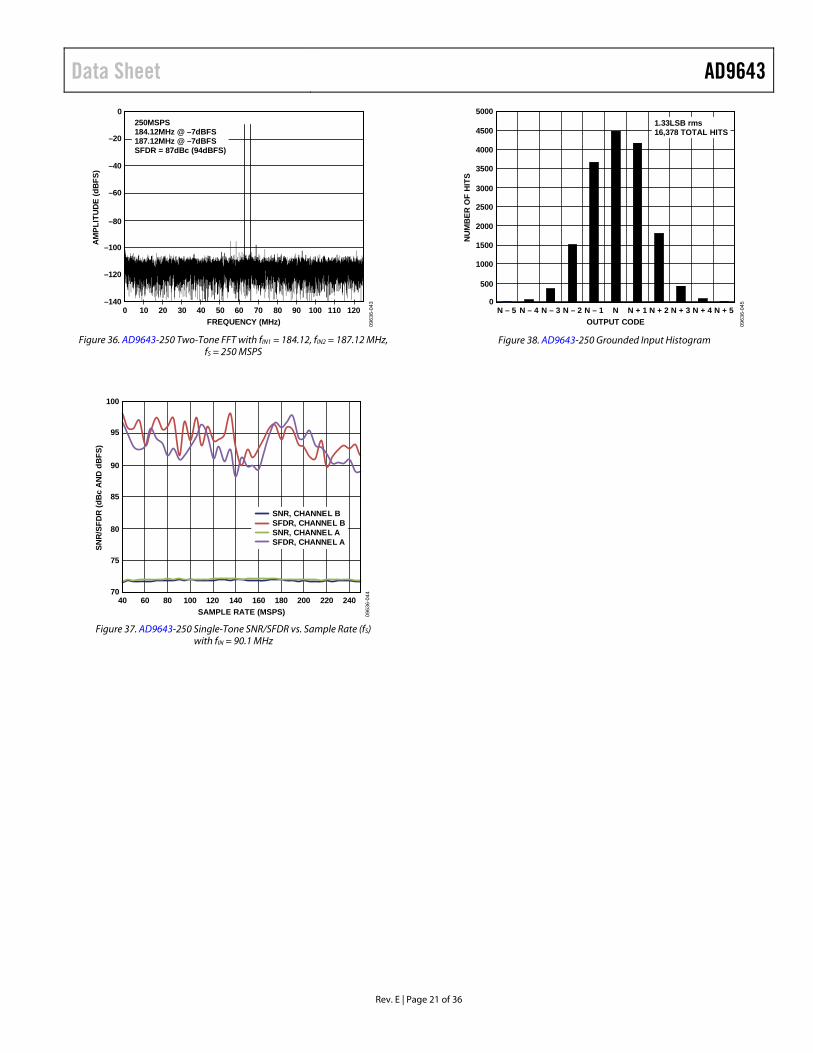
Figure 36. AD9643-250 Two-Tone FFT with fIN1 = 184.12, fIN2 = 187.12 MHz,
fS = 250 MSPS
100
95
90
85
80
75
70220200180160140120100806040 240
SAMPLE RATE (MSPS)
SNR
/SFD
R (d
Bc
AN
D d
BFS
)
0963
6-04
4
SNR, CHANNEL BSFDR, CHANNEL BSNR, CHANNEL ASFDR, CHANNEL A
Figure 37. AD9643-250 Single-Tone SNR/SFDR vs. Sample Rate (fS)
with fIN = 90.1 MHz
5000
4500
4000
3500
3000
2500
2000
1500
1000
500
0N + 2 N + 3 N + 4 N + 5N + 1NN – 1N – 2N – 3N – 4N – 5
OUTPUT CODE
NU
MB
ER O
F H
ITS
0963
6-04
5
1.33LSB rms16,378 TOTAL HITS
Figure 38. AD9643-250 Grounded Input Histogram
AD9643 Data Sheet
Rev. E | Page 22 of 36
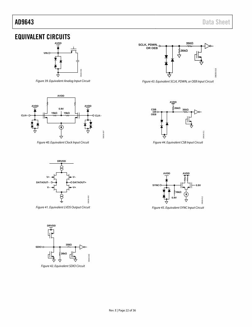
EQUIVALENT CIRCUITS
VIN
AVDD
0963
6-00
6
Figure 39. Equivalent Analog Input Circuit
0.9V15kΩ 15kΩ
CLK+ CLK–
AVDD
0963
6-00
7AVDD AVDD
Figure 40. Equivalent Clock lnput Circuit
0963
6-06
3
DRVDD
DATAOUT+
V–
V+
DATAOUT–
V+
V–
Figure 41. Equivalent LVDS Output Circuit
SDIO350Ω
26kΩ
DRVDD
0963
6-00
9
Figure 42. Equivalent SDIO Circuit
SCLK, PDWN,OR OEB
350Ω
26kΩ
0963
6-01
0
Figure 43. Equivalent SCLK, PDWN, or OEB Input Circuit
CSBOR
OEB
350Ω26kΩ
AVDD
0963
6-01
1
Figure 44. Equivalent CSB Input Circuit
AVDD AVDD
16kΩ
0.9V
0.9VSYNC
0963
6-01
2
Figure 45. Equivalent SYNC Input Circuit
Data Sheet AD9643
Rev. E | Page 23 of 36
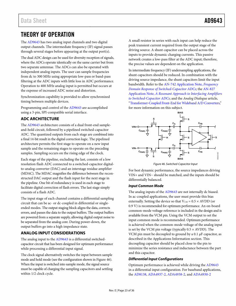
THEORY OF OPERATION The AD9643 has two analog input channels and two digital output channels. The intermediate frequency (IF) signal passes through several stages before appearing at the output port(s).
The dual ADC design can be used for diversity reception of signals, where the ADCs operate identically on the same carrier but from two separate antennae. The ADCs can also be operated with independent analog inputs. The user can sample frequencies from dc to 300 MHz using appropriate low-pass or band-pass filtering at the ADC inputs with little loss in ADC performance. Operation to 400 MHz analog input is permitted but occurs at the expense of increased ADC noise and distortion.
Synchronization capability is provided to allow synchronized timing between multiple devices.
Programming and control of the AD9643 are accomplished using a 3-pin, SPI-compatible serial interface.
ADC ARCHITECTURE The AD9643 architecture consists of a dual front-end sample-and-hold circuit, followed by a pipelined switched-capacitor ADC. The quantized outputs from each stage are combined into a final 14-bit result in the digital correction logic. The pipelined architecture permits the first stage to operate on a new input sample and the remaining stages to operate on the preceding samples. Sampling occurs on the rising edge of the clock.
Each stage of the pipeline, excluding the last, consists of a low resolution flash ADC connected to a switched-capacitor digital-to-analog converter (DAC) and an interstage residue amplifier (MDAC). The MDAC magnifies the difference between the recon-structed DAC output and the flash input for the next stage in the pipeline. One bit of redundancy is used in each stage to facilitate digital correction of flash errors. The last stage simply consists of a flash ADC.
The input stage of each channel contains a differential sampling circuit that can be ac- or dc-coupled in differential or single-ended modes. The output staging block aligns the data, corrects errors, and passes the data to the output buffers. The output buffers are powered from a separate supply, allowing digital output noise to be separated from the analog core. During power-down, the output buffers go into a high impedance state.
ANALOG INPUT CONSIDERATIONS The analog input to the AD9643 is a differential switched-capacitor circuit that has been designed for optimum performance while processing a differential input signal.
The clock signal alternatively switches the input between sample mode and hold mode (see the configuration shown in Figure 46). When the input is switched into sample mode, the signal source must be capable of charging the sampling capacitors and settling within 1/2 clock cycle.
A small resistor in series with each input can help reduce the peak transient current required from the output stage of the driving source. A shunt capacitor can be placed across the inputs to provide dynamic charging currents. This passive network creates a low-pass filter at the ADC input; therefore, the precise values are dependent on the application.
In intermediate frequency (IF) undersampling applications, the shunt capacitors should be reduced. In combination with the driving source impedance, the shunt capacitors limit the input bandwidth. Refer to the AN-742 Application Note, Frequency Domain Response of Switched-Capacitor ADCs; the AN-827 Application Note, A Resonant Approach to Interfacing Amplifiers to Switched-Capacitor ADCs; and the Analog Dialogue article, “Transformer-Coupled Front-End for Wideband A/D Converters,” for more information on this subject.
CPAR1
CPAR1
CPAR2
CPAR2
S
S
S
S
S
S
CFB
CFB
CS
CS
BIAS
BIAS
VIN+
0963
6-05
0
H
VIN–
Figure 46. Switched-Capacitor Input
For best dynamic performance, the source impedances driving VIN+ and VIN− should be matched, and the inputs should be differentially balanced.
Input Common Mode
The analog inputs of the AD9643 are not internally dc biased. In ac-coupled applications, the user must provide this bias externally. Setting the device so that VCM = 0.5 × AVDD (or 0.9 V) is recommended for optimum performance. An on-board common-mode voltage reference is included in the design and is available from the VCM pin. Using the VCM output to set the input common mode is recommended. Optimum performance is achieved when the common-mode voltage of the analog input is set by the VCM pin voltage (typically 0.5 × AVDD). The VCM pin must be decoupled to ground by a 0.1 µF capacitor, as described in the Applications Information section. This decoupling capacitor should be placed close to the pin to minimize the series resistance and inductance between the part and this capacitor.
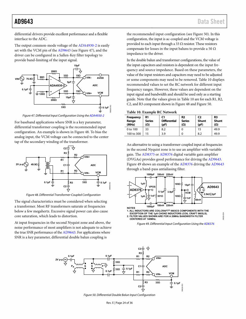
Differential Input Configurations
Optimum performance is achieved while driving the AD9643 in a differential input configuration. For baseband applications, the AD8138, ADA4937-2, ADA4938-2, and ADA4930-2
AD9643 Data Sheet
Rev. E | Page 24 of 36
differential drivers provide excellent performance and a flexible interface to the ADC.
The output common-mode voltage of the ADA4930-2 is easily set with the VCM pin of the AD9643 (see Figure 47), and the driver can be configured in a Sallen-Key filter topology to provide band-limiting of the input signal.
VIN 76.8Ω
120Ω
0.1µF
200Ω
200Ω
90Ω
0.1µF
AVDD33Ω
33Ω
33Ω
15Ω
15Ω
5pF
15pF
15pF
ADC
VIN–
VIN+ VCM
ADA4930-2
0963
6-05
1
Figure 47. Differential Input Configuration Using the ADA4930-2
For baseband applications where SNR is a key parameter, differential transformer coupling is the recommended input configuration. An example is shown in Figure 48. To bias the analog input, the VCM voltage can be connected to the center tap of the secondary winding of the transformer.
2V p-p 49.9Ω
0.1µF
R1
R1
C1 ADC
VIN+
VIN– VCM
C2
R2R3
R2
C2
0963
6-05
2R3 0.1µF33Ω
Figure 48. Differential Transformer-Coupled Configuration
The signal characteristics must be considered when selecting a transformer. Most RF transformers saturate at frequencies below a few megahertz. Excessive signal power can also cause core saturation, which leads to distortion.
At input frequencies in the second Nyquist zone and above, the noise performance of most amplifiers is not adequate to achieve the true SNR performance of the AD9643. For applications where SNR is a key parameter, differential double balun coupling is
the recommended input configuration (see Figure 50). In this configuration, the input is ac-coupled and the VCM voltage is provided to each input through a 33 Ω resistor. These resistors compensate for losses in the input baluns to provide a 50 Ω impedance to the driver.
In the double balun and transformer configurations, the value of the input capacitors and resistors is dependent on the input fre-quency and source impedance. Based on these parameters, the value of the input resistors and capacitors may need to be adjusted or some components may need to be removed. Table 10 displays recommended values to set the RC network for different input frequency ranges. However, these values are dependent on the input signal and bandwidth and should be used only as a starting guide. Note that the values given in Table 10 are for each R1, R2, C2, and R3 component shown in Figure 48 and Figure 50.
Table 10. Example RC Network Frequency Range (MHz)
R1 Series (Ω)
C1 Differential (pF)
R2 Series (Ω)
C2 Shunt (pF)
R3 Shunt (Ω)
0 to 100 33 8.2 0 15 49.9 100 to 300 15 3.9 0 8.2 49.9
An alternative to using a transformer-coupled input at frequencies in the second Nyquist zone is to use an amplifier with variable gain. The AD8375 or AD8376 digital variable gain amplifier (DVGAs) provides good performance for driving the AD9643. Figure 49 shows an example of the AD8376 driving the AD9643 through a band-pass antialiasing filter.
AD8376AD9643
1µH
1µH 1nF1nF
VPOS
VCM
15pF
68nH
2.5kΩ2pF301Ω
165Ω
165Ω
5.1pF 3.9pF
180nH1000pF
1000pFNOTES1. ALL INDUCTORS ARE COILCRAFT® 0603CS COMPONENTS WITH THE EXCEPTION OF THE 1µH CHOKE INDUCTORS (COIL CRAFT 0603LS).2. FILTER VALUES SHOWN ARE FOR A 20MHz BANDWIDTH FILTER CENTERED AT 140MHz.
180nH
220nH
220nH
0963
6-05
4
Figure 49. Differential Input Configuration Using the AD8376
ADC
R10.1µF0.1µF
2V p-pVIN+
VIN– VCM
C1
C2
R1
R2
R20.1µF
S0.1µF
C2
33Ω
33Ω
SPA P
0963
6-05
3
R3
R3 0.1µF33Ω
Figure 50. Differential Double Balun Input Configuration
Data Sheet AD9643
Rev. E | Page 25 of 36
VOLTAGE REFERENCE A stable and accurate voltage reference is built into the AD9643. The full-scale input range can be adjusted by varying the reference voltage via SPI. The input span of the ADC tracks reference voltage changes linearly.
CLOCK INPUT CONSIDERATIONS For optimum performance, the AD9643 sample clock inputs, CLK+ and CLK−, should be clocked with a differential signal. The signal is typically ac-coupled into the CLK+ and CLK− pins via a transformer or via capacitors. These pins are biased internally (see Figure 51) and require no external bias. If the inputs are floated, the CLK− pin is pulled low to prevent spurious clocking.
0963
6-05
5
AVDD
CLK+
4pF4pF
CLK–
0.9V
Figure 51. Simplified Equivalent Clock Input Circuit
Clock Input Options
The AD9643 has a very flexible clock input structure. Clock input can be a CMOS, LVDS, LVPECL, or sine wave signal. Regardless of the type of signal being used, clock source jitter is of the most concern, as described in the Jitter Considerations section.
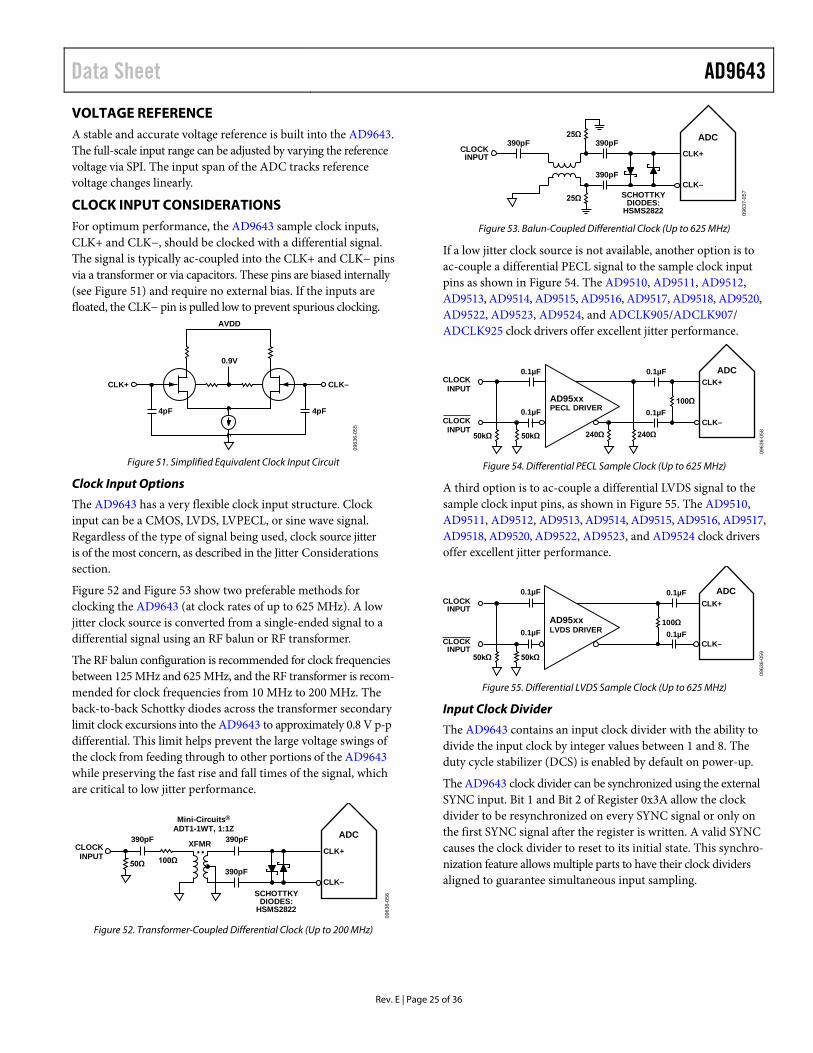
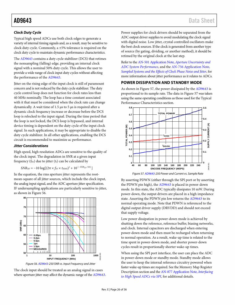
Figure 52 and Figure 53 show two preferable methods for clocking the AD9643 (at clock rates of up to 625 MHz). A low jitter clock source is converted from a single-ended signal to a differential signal using an RF balun or RF transformer.
The RF balun configuration is recommended for clock frequencies between 125 MHz and 625 MHz, and the RF transformer is recom-mended for clock frequencies from 10 MHz to 200 MHz. The back-to-back Schottky diodes across the transformer secondary limit clock excursions into the AD9643 to approximately 0.8 V p-p differential. This limit helps prevent the large voltage swings of the clock from feeding through to other portions of the AD9643 while preserving the fast rise and fall times of the signal, which are critical to low jitter performance.
390pF
390pF390pF
SCHOTTKYDIODES:
HSMS2822
CLOCKINPUT
50Ω 100Ω
CLK–
CLK+
ADCMini-Circuits®
ADT1-1WT, 1:1Z
XFMR
0963
6-05
6
Figure 52. Transformer-Coupled Differential Clock (Up to 200 MHz)
390pF
25Ω
25Ω390pF
390pF
CLOCKINPUT
CLK–
CLK+
SCHOTTKYDIODES:
HSMS2822
ADC
0963
7-05
7
Figure 53. Balun-Coupled Differential Clock (Up to 625 MHz)
If a low jitter clock source is not available, another option is to ac-couple a differential PECL signal to the sample clock input pins as shown in Figure 54. The AD9510, AD9511, AD9512, AD9513, AD9514, AD9515, AD9516, AD9517, AD9518, AD9520, AD9522, AD9523, AD9524, and ADCLK905/ADCLK907/ ADCLK925 clock drivers offer excellent jitter performance.
100Ω0.1µF
0.1µF0.1µF
0.1µF
240Ω240Ω
PECL DRIVER
50kΩ 50kΩCLK–
CLK+CLOCKINPUT
CLOCKINPUT
AD95xx
ADC
0963
6-05
8
Figure 54. Differential PECL Sample Clock (Up to 625 MHz)
A third option is to ac-couple a differential LVDS signal to the sample clock input pins, as shown in Figure 55. The AD9510, AD9511, AD9512, AD9513, AD9514, AD9515, AD9516, AD9517, AD9518, AD9520, AD9522, AD9523, and AD9524 clock drivers offer excellent jitter performance.
100Ω0.1µF
0.1µF0.1µF
0.1µF
50kΩ 50kΩCLK–
CLK+CLOCKINPUT
CLOCKINPUT
AD95xxLVDS DRIVER
ADC
0963
6-05
9
Figure 55. Differential LVDS Sample Clock (Up to 625 MHz)
Input Clock Divider
The AD9643 contains an input clock divider with the ability to divide the input clock by integer values between 1 and 8. The duty cycle stabilizer (DCS) is enabled by default on power-up.
The AD9643 clock divider can be synchronized using the external SYNC input. Bit 1 and Bit 2 of Register 0x3A allow the clock divider to be resynchronized on every SYNC signal or only on the first SYNC signal after the register is written. A valid SYNC causes the clock divider to reset to its initial state. This synchro-nization feature allows multiple parts to have their clock dividers aligned to guarantee simultaneous input sampling.
AD9643 Data Sheet
Rev. E | Page 26 of 36
Clock Duty Cycle
Typical high speed ADCs use both clock edges to generate a variety of internal timing signals and, as a result, may be sensitive to clock duty cycle. Commonly, a ±5% tolerance is required on the clock duty cycle to maintain dynamic performance characteristics.
The AD9643 contains a duty cycle stabilizer (DCS) that retimes the nonsampling (falling) edge, providing an internal clock signal with a nominal 50% duty cycle. This allows the user to provide a wide range of clock input duty cycles without affecting the performance of the AD9643.
Jitter on the rising edge of the input clock is still of paramount concern and is not reduced by the duty cycle stabilizer. The duty cycle control loop does not function for clock rates less than 40 MHz nominally. The loop has a time constant associated with it that must be considered when the clock rate can change dynamically. A wait time of 1.5 µs to 5 µs is required after a dynamic clock frequency increase or decrease before the DCS loop is relocked to the input signal. During the time period that the loop is not locked, the DCS loop is bypassed, and internal device timing is dependent on the duty cycle of the input clock signal. In such applications, it may be appropriate to disable the duty cycle stabilizer. In all other applications, enabling the DCS circuit is recommended to maximize ac performance.
Jitter Considerations
High speed, high resolution ADCs are sensitive to the quality of the clock input. The degradation in SNR at a given input frequency (fIN) due to jitter (tJ) can be calculated by
SNRHF = −10 log[(2π × fIN × tJRMS)2 + 10 )10/( LFSNR− ]
In the equation, the rms aperture jitter represents the root-mean-square of all jitter sources, which include the clock input, the analog input signal, and the ADC aperture jitter specification. IF undersampling applications are particularly sensitive to jitter, as shown in Figure 56.
80
75
70
65
60
55
501 10 100 1000
INPUT FREQUENCY (MHz)
SNR
(dB
c)
0963
6-06
0
0.05ps0.2ps0.5ps1ps1.5psMEASURED
Figure 56. AD9643-250 SNR vs. Input Frequency and Jitter
The clock input should be treated as an analog signal in cases where aperture jitter may affect the dynamic range of the AD9643.
Power supplies for clock drivers should be separated from the ADC output driver supplies to avoid modulating the clock signal with digital noise. Low jitter, crystal controlled oscillators make the best clock sources. If the clock is generated from another type of source (by gating, dividing, or another method), it should be retimed by the original clock at the last step.
Refer to the AN-501 Application Note, Aperture Uncertainty and ADC System Performance, and the AN-756 Application Note, Sampled Systems and the Effects of Clock Phase Noise and Jitter, for more information about jitter performance as it relates to ADCs.
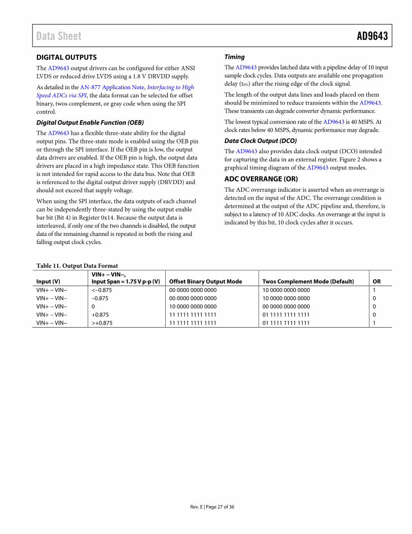
POWER DISSIPATION AND STANDBY MODE As shown in Figure 57, the power dissipated by the AD9643 is proportional to its sample rate. The data in Figure 57 was taken using the same operating conditions as those used for the Typical Performance Characteristics section.
0.8
0.7
0.6
0.5
0.4
0.3
0.2
0.1
0.5
0.4
0.3
0.2
0.1
0040 60 80 100 120 140 160 180 200 220 240
ENCODE FREQUENCY (MSPS)
TOTA
L PO
WER
(W)
SUPP
LY C
UR
REN
T (A
)09
636-
061
TOTAL POWER
IAVDD
IDRVDD
Figure 57. AD9643-250 Power and Current vs. Sample Rate
By asserting PDWN (either through the SPI port or by asserting the PDWN pin high), the AD9643 is placed in power-down mode. In this state, the ADC typically dissipates 10 mW. During power-down, the output drivers are placed in a high impedance state. Asserting the PDWN pin low returns the AD9643 to its normal operating mode. Note that PDWN is referenced to the digital output driver supply (DRVDD) and should not exceed that supply voltage.
Low power dissipation in power-down mode is achieved by shutting down the reference, reference buffer, biasing networks, and clock. Internal capacitors are discharged when entering power-down mode and then must be recharged when returning to normal operation. As a result, wake-up time is related to the time spent in power-down mode, and shorter power-down cycles result in proportionally shorter wake-up times.
When using the SPI port interface, the user can place the ADC in power-down mode or standby mode. Standby mode allows the user to keep the internal reference circuitry powered when faster wake-up times are required. See the Memory Map Register Description section and the AN-877 Application Note, Interfacing to High Speed ADCs via SPI, for additional details.
Data Sheet AD9643
Rev. E | Page 27 of 36
DIGITAL OUTPUTS The AD9643 output drivers can be configured for either ANSI LVDS or reduced drive LVDS using a 1.8 V DRVDD supply.
As detailed in the AN-877 Application Note, Interfacing to High Speed ADCs via SPI, the data format can be selected for offset binary, twos complement, or gray code when using the SPI control.
Digital Output Enable Function (OEB)
The AD9643 has a flexible three-state ability for the digital output pins. The three-state mode is enabled using the OEB pin or through the SPI interface. If the OEB pin is low, the output data drivers are enabled. If the OEB pin is high, the output data drivers are placed in a high impedance state. This OEB function is not intended for rapid access to the data bus. Note that OEB is referenced to the digital output driver supply (DRVDD) and should not exceed that supply voltage.
When using the SPI interface, the data outputs of each channel can be independently three-stated by using the output enable bar bit (Bit 4) in Register 0x14. Because the output data is interleaved, if only one of the two channels is disabled, the output data of the remaining channel is repeated in both the rising and falling output clock cycles.
Timing
The AD9643 provides latched data with a pipeline delay of 10 input sample clock cycles. Data outputs are available one propagation delay (tPD) after the rising edge of the clock signal.
The length of the output data lines and loads placed on them should be minimized to reduce transients within the AD9643. These transients can degrade converter dynamic performance.
The lowest typical conversion rate of the AD9643 is 40 MSPS. At clock rates below 40 MSPS, dynamic performance may degrade.
Data Clock Output (DCO)
The AD9643 also provides data clock output (DCO) intended for capturing the data in an external register. Figure 2 shows a graphical timing diagram of the AD9643 output modes.
ADC OVERRANGE (OR) The ADC overrange indicator is asserted when an overrange is detected on the input of the ADC. The overrange condition is determined at the output of the ADC pipeline and, therefore, is subject to a latency of 10 ADC clocks. An overrange at the input is indicated by this bit, 10 clock cycles after it occurs.
Table 11. Output Data Format
Input (V) VIN+ − VIN−, Input Span = 1.75 V p-p (V) Offset Binary Output Mode Twos Complement Mode (Default) OR
VIN+ − VIN− <–0.875 00 0000 0000 0000 10 0000 0000 0000 1 VIN+ − VIN− –0.875 00 0000 0000 0000 10 0000 0000 0000 0 VIN+ − VIN− 0 10 0000 0000 0000 00 0000 0000 0000 0 VIN+ − VIN− +0.875 11 1111 1111 1111 01 1111 1111 1111 0 VIN+ − VIN− >+0.875 11 1111 1111 1111 01 1111 1111 1111 1
AD9643 Data Sheet
Rev. E | Page 28 of 36
CHANNEL/CHIP SYNCHRONIZATION The AD9643 has a SYNC input that allows the user flexible synchronization options for synchronizing the internal blocks. The SYNC feature is useful for guaranteeing synchronized operation across multiple ADCs. The input clock divider can be synchronized using the SYNC input. The divider can be enabled to synchronize on a single occurrence of the SYNC signal or on every occurrence by setting the appropriate bits in Register 0x3A.
The SYNC input is internally synchronized to the sample clock. However, to ensure that there is no timing uncertainty between multiple parts, the SYNC input signal should be synchronized to the input clock signal. The SYNC input should be driven using a single-ended CMOS type signal.
Data Sheet AD9643
Rev. E | Page 29 of 36
SERIAL PORT INTERFACE (SPI) The AD9643 serial port interface (SPI) allows the user to configure the converter for specific functions or operations through a structured register space provided inside the ADC. The SPI gives the user added flexibility and customization, depending on the application. Addresses are accessed via the serial port and can be written to or read from via the port. Memory is organized into bytes that can be further divided into fields. These fields are documented in the Memory Map section. For detailed operational information, see the AN-877 Application Note, Interfacing to High Speed ADCs via SPI.
CONFIGURATION USING THE SPI Three pins define the SPI of this ADC: the SCLK pin, the SDIO pin, and the CSB pin (see Table 12). The SCLK (serial clock) pin is used to synchronize the read and write data presented from/to the ADC. The SDIO (serial data input/output) pin is a dual-purpose pin that allows data to be sent and read from the internal ADC memory map registers. The CSB (chip select bar) pin is an active low control that enables or disables the read and write cycles.
Table 12. Serial Port Interface Pins Pin Function SCLK Serial Clock. The serial shift clock input, which is used to
synchronize serial interface reads and writes. SDIO Serial Data Input/Output. A dual-purpose pin that
typically serves as an input or an output, depending on the instruction being sent and the relative position in the timing frame.
CSB Chip Select Bar. An active low control that gates the read and write cycles.
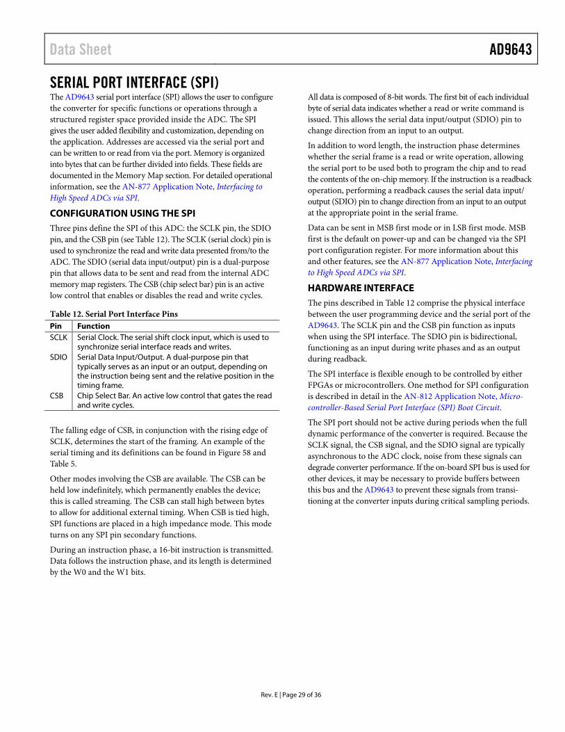
The falling edge of CSB, in conjunction with the rising edge of SCLK, determines the start of the framing. An example of the serial timing and its definitions can be found in Figure 58 and Table 5.
Other modes involving the CSB are available. The CSB can be held low indefinitely, which permanently enables the device; this is called streaming. The CSB can stall high between bytes to allow for additional external timing. When CSB is tied high, SPI functions are placed in a high impedance mode. This mode turns on any SPI pin secondary functions.
During an instruction phase, a 16-bit instruction is transmitted. Data follows the instruction phase, and its length is determined by the W0 and the W1 bits.
All data is composed of 8-bit words. The first bit of each individual byte of serial data indicates whether a read or write command is issued. This allows the serial data input/output (SDIO) pin to change direction from an input to an output.
In addition to word length, the instruction phase determines whether the serial frame is a read or write operation, allowing the serial port to be used both to program the chip and to read the contents of the on-chip memory. If the instruction is a readback operation, performing a readback causes the serial data input/ output (SDIO) pin to change direction from an input to an output at the appropriate point in the serial frame.
Data can be sent in MSB first mode or in LSB first mode. MSB first is the default on power-up and can be changed via the SPI port configuration register. For more information about this and other features, see the AN-877 Application Note, Interfacing to High Speed ADCs via SPI.
HARDWARE INTERFACE The pins described in Table 12 comprise the physical interface between the user programming device and the serial port of the AD9643. The SCLK pin and the CSB pin function as inputs when using the SPI interface. The SDIO pin is bidirectional, functioning as an input during write phases and as an output during readback.
The SPI interface is flexible enough to be controlled by either FPGAs or microcontrollers. One method for SPI configuration is described in detail in the AN-812 Application Note, Micro-controller-Based Serial Port Interface (SPI) Boot Circuit.
The SPI port should not be active during periods when the full dynamic performance of the converter is required. Because the SCLK signal, the CSB signal, and the SDIO signal are typically asynchronous to the ADC clock, noise from these signals can degrade converter performance. If the on-board SPI bus is used for other devices, it may be necessary to provide buffers between this bus and the AD9643 to prevent these signals from transi-tioning at the converter inputs during critical sampling periods.
AD9643 Data Sheet
Rev. E | Page 30 of 36
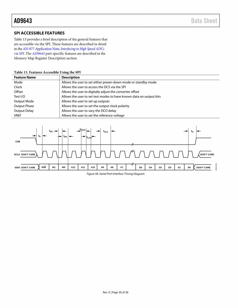
SPI ACCESSIBLE FEATURES Table 13 provides a brief description of the general features that are accessible via the SPI. These features are described in detail in the AN-877 Application Note, Interfacing to High Speed ADCs via SPI. The AD9643 part-specific features are described in the Memory Map Register Description section.
Table 13. Features Accessible Using the SPI Feature Name Description Mode Allows the user to set either power-down mode or standby mode Clock Allows the user to access the DCS via the SPI Offset Allows the user to digitally adjust the converter offset Test I/O Allows the user to set test modes to have known data on output bits Output Mode Allows the user to set up outputs Output Phase Allows the user to set the output clock polarity Output Delay Allows the user to vary the DCO delay VREF Allows the user to set the reference voltage
DON’T CARE
DON’T CAREDON’T CARE
DON’T CARE
SDIO
SCLK
CSB
tS tDH
tCLKtDS tH
R/W W1 W0 A12 A11 A10 A9 A8 A7 D5 D4 D3 D2 D1 D0
tLOW
tHIGH
0963
6-06
2
Figure 58. Serial Port Interface Timing Diagram
Data Sheet AD9643
Rev. E | Page 31 of 36
MEMORY MAP READING THE MEMORY MAP REGISTER TABLE Each row in the memory map register table has eight bit locations. The memory map is roughly divided into three sections: the chip configuration registers (Address 0x00 to Address 0x02); the channel index and transfer registers (Address 0x05 and Address 0xFF); and the ADC functions registers, including setup, control, and test (Address 0x08 to Address 0x3A).
The memory map register table (see Table 14) documents the default hexadecimal value for each hexadecimal address shown. The column with the heading Bit 7 (MSB) is the start of the default hexadecimal value given. For example, Address 0x14, the output mode register, has a hexadecimal default value of 0x05. This means that Bit 0 = 1 and Bit 2 = 1, and the remaining bits are 0s. This setting is the default output format value, which is twos complement. For more information on this function and others, see the AN-877 Application Note, Interfacing to High Speed ADCs via SPI. This document details the functions controlled by Register 0x00 to Register 0x20. The remaining registers, Register 0x3A, is documented in the Memory Map Register Description section.
Open and Reserved Locations
All address and bit locations that are not included in Table 14 are not currently supported for this device. Unused bits of a valid address location should be written with 0s. Writing to these locations is required only when part of an address location is open (for example, Address 0x18). If the entire address location is open (for example, Address 0x13), this address location should not be written.
Default Values
After the AD9643 is reset, critical registers are loaded with default values. The default values for the registers are given in the memory map register table, Table 14.
Logic Levels
An explanation of logic level terminology follows:
• “Bit is set” is synonymous with “bit is set to Logic 1” or “writing Logic 1 for the bit.”
• “Clear a bit” is synonymous with “bit is set to Logic 0” or “writing Logic 0 for the bit.”
Transfer Register Map
Address 0x08 to Address 0x20 and Address 0x3A are shadowed. Writes to these addresses do not affect part operation until a transfer command is issued by writing 0x01 to Address 0xFF, setting the transfer bit. This allows these registers to be updated internally and simultaneously when the transfer bit is set. The internal update takes place when the transfer bit is set, and then the bit autoclears.
Channel-Specific Registers
Some channel setup functions, such as the signal monitor thresholds, can be programmed to a different value for each channel. In these cases, channel address locations are internally duplicated for each channel. These registers and bits are designated in Table 14 as local. These local registers and bits can be accessed by setting the appropriate Channel A or Channel B bits in Register 0x05. If both bits are set, the subsequent write affects the registers of both channels. In a read cycle, only Channel A or Channel B should be set to read one of the two registers. If both bits are set during an SPI read cycle, the part returns the value for Channel A. Registers and bits designated as global in Table 14 affect the entire part and the channel features for which independent settings are not allowed between channels. The settings in Register 0x05 do not affect the global registers and bits.
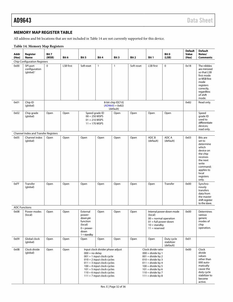
AD9643 Data Sheet
Rev. E | Page 32 of 36
MEMORY MAP REGISTER TABLE All address and bit locations that are not included in Table 14 are not currently supported for this device.
Table 14. Memory Map Registers
Addr (Hex)
Register Name
Bit 7 (MSB) Bit 6 Bit 5 Bit 4 Bit 3 Bit 2 Bit 1
Bit 0 (LSB)
Default Value (Hex)
Default Notes/ Comments
Chip Configuration Registers
0x00 SPI port configuration (global)1
0 LSB first Soft reset 1 1 Soft reset LSB first 0 0x18 The nibbles are mirrored so that LSB first mode or MSB first mode registers correctly, regardless of shift mode.
0x01 Chip ID (global)
8-bit chip ID[7:0] (AD9643 = 0x82)
(default)
0x82 Read only.
0x02 Chip grade (global)
Open Open Speed grade ID 00 = 250 MSPS 01 = 210 MSPS 11 = 170 MSPS
Open Open Open Open Speed grade ID used to differentiate devices; read only.
Channel Index and Transfer Registers
0x05 Channel index (global)
Open Open Open Open Open Open ADC B (default)
ADC A (default)
0x03 Bits are set to determine which device on the chip receives the next write command; applies to local registers only.
0xFF Transfer (global)
Open Open Open Open Open Open Open Transfer 0x00 Synchro-nously transfers data from the master shift register to the slave.
ADC Functions
0x08 Power modes (local)
Open Open External power-down pin function (local) 0 = power-down 1 = standby
Open Open Open Internal power-down mode (local) 00 = normal operation 01 = full power-down 10 = standby 11 = reserved
0x00 Determines various generic modes of chip operation.
0x09 Global clock (global)
Open Open Open Open Open Open Open Duty cycle stabilizer (default)
0x01
0x0B Clock divide (global)
Open Open Input clock divider phase adjust 000 = no delay 001 = 1 input clock cycle 010 = 2 input clock cycles 011 = 3 input clock cycles 100 = 4 input clock cycles 101 = 5 input clock cycles 110 = 6 input clock cycles 111 = 7 input clock cycles
Clock divide ratio 000 = divide by 1 001 = divide by 2 010 = divide by 3 011 = divide by 4 100 = divide by 5 101 = divide by 6 110 = divide by 7 111 = divide by 8
0x00 Clock divide values other than 000 auto-matically cause the duty cycle stabilizer to become active.
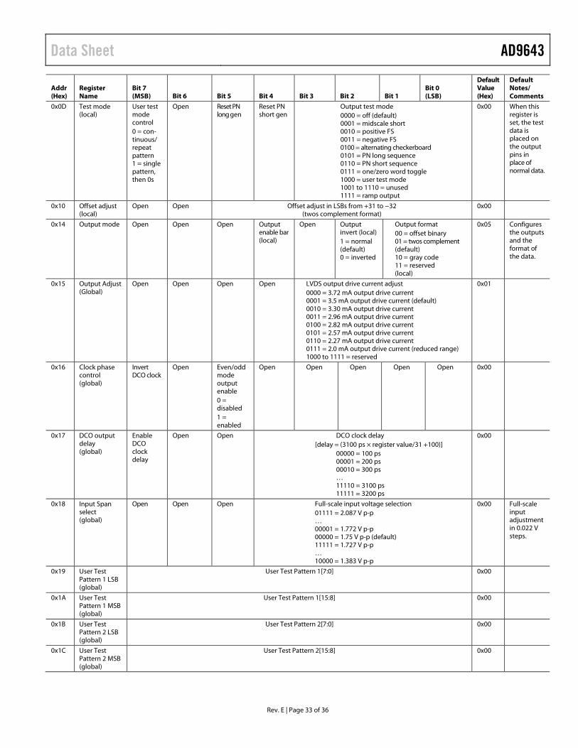
Data Sheet AD9643
Rev. E | Page 33 of 36
Addr (Hex)
Register Name
Bit 7 (MSB) Bit 6 Bit 5 Bit 4 Bit 3 Bit 2 Bit 1
Bit 0 (LSB)
Default Value (Hex)
Default Notes/ Comments
0x0D Test mode (local)
User test mode control 0 = con-tinuous/ repeat pattern 1 = single pattern, then 0s
Open Reset PN long gen
Reset PN short gen
Output test mode 0000 = off (default) 0001 = midscale short 0010 = positive FS 0011 = negative FS 0100 = alternating checkerboard 0101 = PN long sequence 0110 = PN short sequence 0111 = one/zero word toggle 1000 = user test mode 1001 to 1110 = unused 1111 = ramp output
0x00 When this register is set, the test data is placed on the output pins in place of normal data.
0x10 Offset adjust (local)
Open Open Offset adjust in LSBs from +31 to −32 (twos complement format)
0x00
0x14 Output mode Open Open Open Output enable bar (local)
Open Output invert (local) 1 = normal (default) 0 = inverted
Output format 00 = offset binary 01 = twos complement (default) 10 = gray code 11 = reserved (local)
0x05 Configures the outputs and the format of the data.
0x15 Output Adjust (Global)
Open Open Open Open LVDS output drive current adjust 0000 = 3.72 mA output drive current 0001 = 3.5 mA output drive current (default) 0010 = 3.30 mA output drive current 0011 = 2.96 mA output drive current 0100 = 2.82 mA output drive current 0101 = 2.57 mA output drive current 0110 = 2.27 mA output drive current 0111 = 2.0 mA output drive current (reduced range) 1000 to 1111 = reserved
0x01
0x16 Clock phase control (global)
Invert DCO clock
Open Even/odd mode output enable 0 = disabled 1 = enabled
Open Open Open Open Open 0x00
0x17 DCO output delay (global)
Enable DCO clock delay
Open Open DCO clock delay [delay = (3100 ps × register value/31 +100)]
00000 = 100 ps 00001 = 200 ps 00010 = 300 ps … 11110 = 3100 ps 11111 = 3200 ps
0x00
0x18 Input Span select (global)
Open Open Open Full-scale input voltage selection 01111 = 2.087 V p-p … 00001 = 1.772 V p-p 00000 = 1.75 V p-p (default) 11111 = 1.727 V p-p … 10000 = 1.383 V p-p
0x00 Full-scale input adjustment in 0.022 V steps.
0x19 User Test Pattern 1 LSB (global)
User Test Pattern 1[7:0] 0x00
0x1A User Test Pattern 1 MSB (global)
User Test Pattern 1[15:8] 0x00
0x1B User Test Pattern 2 LSB (global)
User Test Pattern 2[7:0] 0x00
0x1C User Test Pattern 2 MSB (global)
User Test Pattern 2[15:8] 0x00
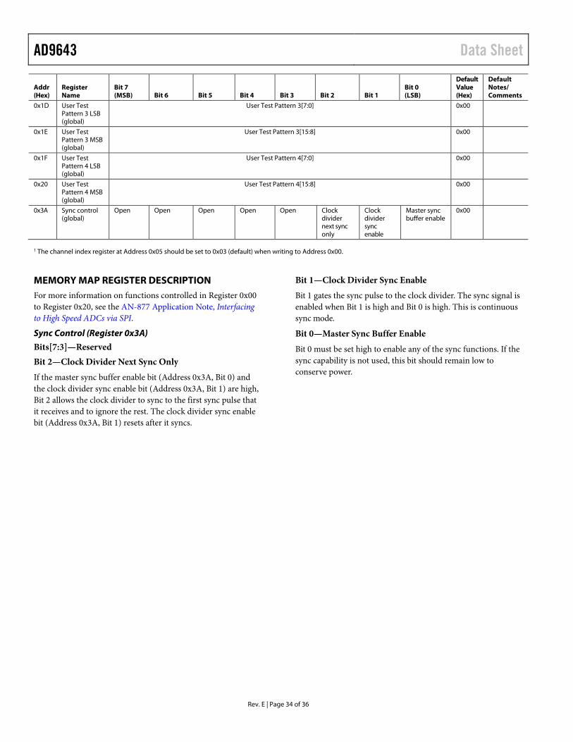
AD9643 Data Sheet
Rev. E | Page 34 of 36
Addr (Hex)
Register Name
Bit 7 (MSB) Bit 6 Bit 5 Bit 4 Bit 3 Bit 2 Bit 1
Bit 0 (LSB)
Default Value (Hex)
Default Notes/ Comments
0x1D User Test Pattern 3 LSB (global)
User Test Pattern 3[7:0] 0x00
0x1E User Test Pattern 3 MSB (global)
User Test Pattern 3[15:8] 0x00
0x1F User Test Pattern 4 LSB (global)
User Test Pattern 4[7:0] 0x00
0x20 User Test Pattern 4 MSB (global)
User Test Pattern 4[15:8] 0x00
0x3A Sync control (global)
Open Open Open Open Open Clock divider next sync only
Clock divider sync enable
Master sync buffer enable
0x00
1 The channel index register at Address 0x05 should be set to 0x03 (default) when writing to Address 0x00.
MEMORY MAP REGISTER DESCRIPTION For more information on functions controlled in Register 0x00 to Register 0x20, see the AN-877 Application Note, Interfacing to High Speed ADCs via SPI.
Sync Control (Register 0x3A)
Bits[7:3]—Reserved Bit 2—Clock Divider Next Sync Only
If the master sync buffer enable bit (Address 0x3A, Bit 0) and the clock divider sync enable bit (Address 0x3A, Bit 1) are high, Bit 2 allows the clock divider to sync to the first sync pulse that it receives and to ignore the rest. The clock divider sync enable bit (Address 0x3A, Bit 1) resets after it syncs.
Bit 1—Clock Divider Sync Enable
Bit 1 gates the sync pulse to the clock divider. The sync signal is enabled when Bit 1 is high and Bit 0 is high. This is continuous sync mode.
Bit 0—Master Sync Buffer Enable
Bit 0 must be set high to enable any of the sync functions. If the sync capability is not used, this bit should remain low to conserve power.
Data Sheet AD9643
Rev. E | Page 35 of 36
APPLICATIONS INFORMATION DESIGN GUIDELINES Before starting system level design and layout of the AD9643, it is recommended that the designer become familiar with these guidelines, which discuss the special circuit connections and layout requirements needed for certain pins.
Power and Ground Recommendations
When connecting power to the AD9643, it is recommended that two separate 1.8 V supplies be used: one supply should be used for analog (AVDD), and a separate supply should be used for the digital outputs (DRVDD). The designer can employ several different decoupling capacitors to cover both high and low frequencies. These capacitors should be located close to the point of entry at the PC board level and close to the pins of the part with minimal trace length.
A single PCB ground plane should be sufficient when using the AD9643. With proper decoupling and smart partitioning of the PCB analog, digital, and clock sections, optimum performance is easily achieved.
Exposed Paddle Thermal Heat Slug Recommendations
It is mandatory that the exposed paddle on the underside of the ADC be connected to analog ground (AGND) to achieve the best electrical and thermal performance. A continuous, exposed (no solder mask) copper plane on the PCB should mate to the AD9643 exposed paddle, Pin 0.
The copper plane should have several vias to achieve the lowest possible resistive thermal path for heat dissipation to flow through the bottom of the PCB. These vias should be filled or plugged with nonconductive epoxy.
To maximize the coverage and adhesion between the ADC and the PCB, a silkscreen should be overlaid to partition the continuous plane on the PCB into several uniform sections. This provides several tie points between the ADC and the PCB during the reflow process. Using one continuous plane with no partitions guarantees only one tie point between the ADC and the PCB. See the evaluation board for a PCB layout example. For detailed information about the packaging and PCB layout of chip scale packages, refer to the AN-772 Application Note, A Design and Manufacturing Guide for the Lead Frame Chip Scale Package (LFCSP).
VCM
The VCM pin should be decoupled to ground with a 0.1 μF capacitor, as shown in Figure 48. For optimal channel-to-channel isolation, a 33 Ω resistor should be included between the AD9643 VCM pin and the Channel A analog input network connection, as well as between the AD9643 VCM pin and the Channel B analog input network connection.
SPI Port
The SPI port should not be active during periods when the full dynamic performance of the converter is required. Because the SCLK, CSB, and SDIO signals are typically asynchronous to the ADC clock, noise from these signals can degrade converter performance. If the on-board SPI bus is used for other devices, it may be necessary to provide buffers between this bus and the AD9643 to keep these signals from transitioning at the converter input pins during critical sampling periods.
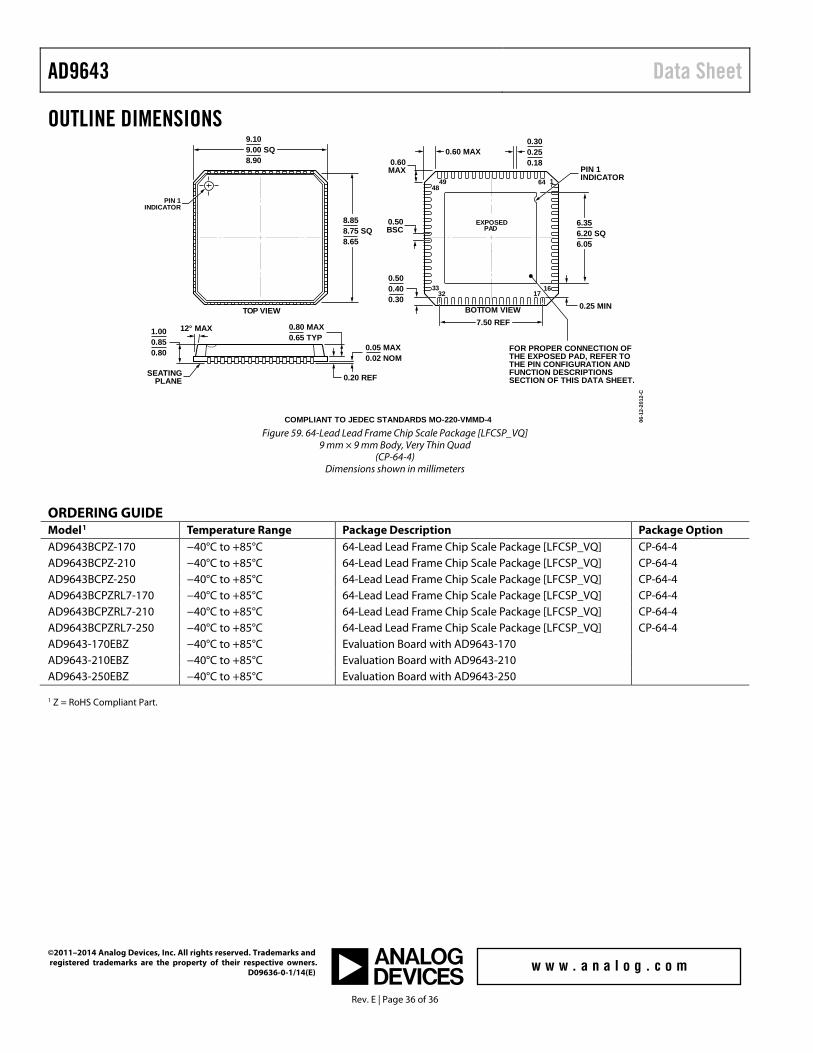
AD9643 Data Sheet
Rev. E | Page 36 of 36
OUTLINE DIMENSIONS
COMPLIANT TO JEDEC STANDARDS MO-220-VMMD-4
0.25 MIN
164
1617
4948
3233
0.500.400.30
0.50BSC
0.20 REF
12° MAX 0.80 MAX0.65 TYP
1.000.850.80
7.50 REF
0.05 MAX0.02 NOM
0.60 MAX0.60MAX
SEATINGPLANE
PIN 1INDICATOR
6.356.20 SQ6.05
PIN 1INDICATOR
0.300.250.18
FOR PROPER CONNECTION OFTHE EXPOSED PAD, REFER TOTHE PIN CONFIGURATION ANDFUNCTION DESCRIPTIONSSECTION OF THIS DATA SHEET.
TOP VIEW
EXPOSEDPAD
BOTTOM VIEW
9.109.00 SQ8.90
8.858.75 SQ8.65
06-1
2-20
12-C
Figure 59. 64-Lead Lead Frame Chip Scale Package [LFCSP_VQ]
9 mm × 9 mm Body, Very Thin Quad (CP-64-4)
Dimensions shown in millimeters
ORDERING GUIDE Model1 Temperature Range Package Description Package Option AD9643BCPZ-170 −40°C to +85°C 64-Lead Lead Frame Chip Scale Package [LFCSP_VQ] CP-64-4 AD9643BCPZ-210 −40°C to +85°C 64-Lead Lead Frame Chip Scale Package [LFCSP_VQ] CP-64-4 AD9643BCPZ-250 −40°C to +85°C 64-Lead Lead Frame Chip Scale Package [LFCSP_VQ] CP-64-4 AD9643BCPZRL7-170 −40°C to +85°C 64-Lead Lead Frame Chip Scale Package [LFCSP_VQ] CP-64-4 AD9643BCPZRL7-210 −40°C to +85°C 64-Lead Lead Frame Chip Scale Package [LFCSP_VQ] CP-64-4 AD9643BCPZRL7-250 −40°C to +85°C 64-Lead Lead Frame Chip Scale Package [LFCSP_VQ] CP-64-4 AD9643-170EBZ −40°C to +85°C Evaluation Board with AD9643-170 AD9643-210EBZ −40°C to +85°C Evaluation Board with AD9643-210 AD9643-250EBZ −40°C to +85°C Evaluation Board with AD9643-250 1 Z = RoHS Compliant Part.
©2011–2014 Analog Devices, Inc. All rights reserved. Trademarks and registered trademarks are the property of their respective owners. D09636-0-1/14(E)