Embed Size (px)
Citation preview
DSP56300 FAMILY MANUAL
24-Bit Digital Signal Processor
DSP56300FM/ADRevision 3.0, November 2000
Motorola reserves the right to make changes without further notice to any products herein. Motorola makes no warranty,representation or guarantee regarding the suitability of its products for any particular purpose, nor does Motorola assume anyliability arising out of the application or use of any product or circuit, and specifically disclaims any and all liability, includingwithout limitation consequential or incidental damages. “Typical” parameters which may be provided in Motorola data sheetsand/or specifications can and do vary in different applications and actual performance may vary over time. All operatingparameters, including “Typicals” must be validated for each customer application by customer’s technical experts. Motorola doesnot convey any license under its patent rights nor the rights of others. Motorola products are not designed, intended, or authorizedfor use as components in systems intended for surgical implant into the body, or other applications intended to support life, or forany other application in which the failure of the Motorola product could create a situation where personal injury or death mayoccur. Should Buyer purchase or use Motorola products for any such unintended or unauthorized application, Buyer shallindemnify and hold Motorola and its officers, employees, subsidiaries, affiliates, and distributors harmless against all claims,costs, damages, and expenses, and reasonable attorney fees arising out of, directly or indirectly, any claim of personal injury ordeath associated with such unintended or unauthorized use, even if such claim alleges that Motorola was negligent regarding thedesign or manufacture of the part. Motorola and are registered trademarks of Motorola, Inc. Motorola, Inc. is an EqualOpportunity/Affirmative Action Employer.
OnCE, DigitalDNA, and the DigitalDNA logo are trademarks of Motorola, Inc.
How to reach us:
USA/EUROPEMotorola Literature DistributionP.O. Box 5405Denver, Colorado 802171-303-675-21401-800-441-2447
Technical Information Center1-800-521-6274
JAPANMotorola Japan Ltd.SPS, Technical Information Center3-20-1, Minami-Azabu, Minato-kuTokyo 106-8573 Japan81-3-3440-3569
ASIA/PACIFICMotorola Semiconductors H.K. Ltd.Silicon Harbour Centre2 Dai King StreetTai Po Industrial EstateTai Po, N.T., Hong Kong852-26668334
Home Pagehttp://www.mot.com/SPS/DSP
DSP Helplinehttp://www.motorola-dsp.com/contactemail: [email protected]
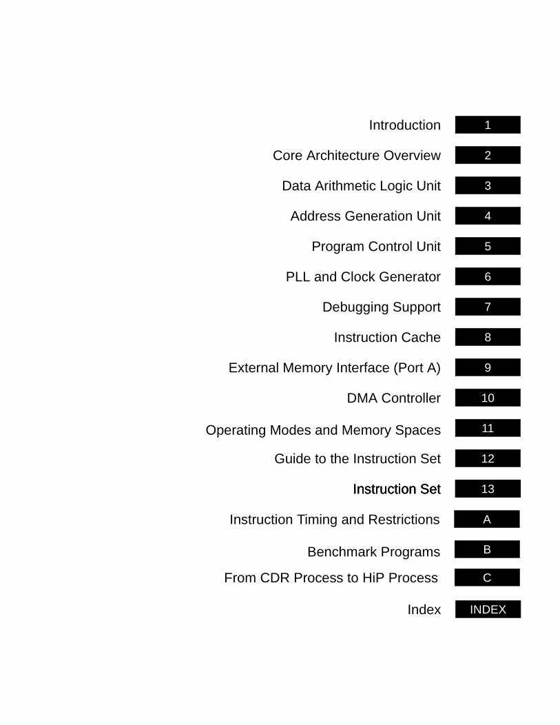
1
2
3
4
5
6
7
8
9
10
11
12
13
Introduction
Core Architecture Overview
Data Arithmetic Logic Unit
Address Generation Unit
Program Control Unit
PLL and Clock Generator
Debugging Support
Instruction Cache
External Memory Interface (Port A)
DMA Controller
Operating Modes and Memory Spaces
Guide to the Instruction Set
Instruction Set 13Instruction Set 13Instruction Set
AInstruction Timing and Restrictions
BBenchmark Programs
CFrom CDR Process to HiP Process
INDEXIndex
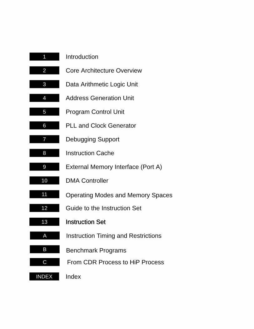
1
2
3
4
5
6
7
8
9
10
11
12
13
Introduction
Core Architecture Overview
Data Arithmetic Logic Unit
Address Generation Unit
Program Control Unit
PLL and Clock Generator
Debugging Support
Instruction Cache
External Memory Interface (Port A)
DMA Controller
Operating Modes and Memory Spaces
Guide to the Instruction Set
Instruction Set13 Instruction Set13 Instruction Set
A Instruction Timing and Restrictions
B Benchmark Programs
C From CDR Process to HiP Process
INDEX Index
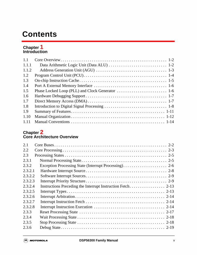
Contents
Chapter 1 Introduction
1.1 Core Overview. . . . . . . . . . . . . . . . . . . . . . . . . . . . . . . . . . . . . . . . . . . . . . . . . . . 1-21.1.1 Data Arithmetic Logic Unit (Data ALU) . . . . . . . . . . . . . . . . . . . . . . . . . . . . 1-21.1.2 Address Generation Unit (AGU) . . . . . . . . . . . . . . . . . . . . . . . . . . . . . . . . . . 1-31.2 Program Control Unit (PCU). . . . . . . . . . . . . . . . . . . . . . . . . . . . . . . . . . . . . . . . 1-41.3 On-chip Instruction Cache . . . . . . . . . . . . . . . . . . . . . . . . . . . . . . . . . . . . . . . . . . 1-51.4 Port A External Memory Interface . . . . . . . . . . . . . . . . . . . . . . . . . . . . . . . . . . . 1-61.5 Phase Locked Loop (PLL) and Clock Generator . . . . . . . . . . . . . . . . . . . . . . . . 1-61.6 Hardware Debugging Support . . . . . . . . . . . . . . . . . . . . . . . . . . . . . . . . . . . . . . . 1-71.7 Direct Memory Access (DMA) . . . . . . . . . . . . . . . . . . . . . . . . . . . . . . . . . . . . . . 1-71.8 Introduction to Digital Signal Processing . . . . . . . . . . . . . . . . . . . . . . . . . . . . . . 1-81.9 Summary of Features . . . . . . . . . . . . . . . . . . . . . . . . . . . . . . . . . . . . . . . . . . . . . 1-111.10 Manual Organization . . . . . . . . . . . . . . . . . . . . . . . . . . . . . . . . . . . . . . . . . . . . . 1-121.11 Manual Conventions . . . . . . . . . . . . . . . . . . . . . . . . . . . . . . . . . . . . . . . . . . . . . 1-14
Chapter 2 Core Architecture Overview
2.1 Core Buses . . . . . . . . . . . . . . . . . . . . . . . . . . . . . . . . . . . . . . . . . . . . . . . . . . . . . . 2-22.2 Core Processing . . . . . . . . . . . . . . . . . . . . . . . . . . . . . . . . . . . . . . . . . . . . . . . . . . 2-32.3 Processing States . . . . . . . . . . . . . . . . . . . . . . . . . . . . . . . . . . . . . . . . . . . . . . . . . 2-52.3.1 Normal Processing State. . . . . . . . . . . . . . . . . . . . . . . . . . . . . . . . . . . . . . . . . 2-52.3.2 Exception Processing State (Interrupt Processing). . . . . . . . . . . . . . . . . . . . . 2-62.3.2.1 Hardware Interrupt Source . . . . . . . . . . . . . . . . . . . . . . . . . . . . . . . . . . . . . . . 2-82.3.2.2 Software Interrupt Sources. . . . . . . . . . . . . . . . . . . . . . . . . . . . . . . . . . . . . . . 2-92.3.2.3 Interrupt Priority Structure . . . . . . . . . . . . . . . . . . . . . . . . . . . . . . . . . . . . . . . 2-92.3.2.4 Instructions Preceding the Interrupt Instruction Fetch. . . . . . . . . . . . . . . . . 2-132.3.2.5 Interrupt Types . . . . . . . . . . . . . . . . . . . . . . . . . . . . . . . . . . . . . . . . . . . . . . . 2-132.3.2.6 Interrupt Arbitration . . . . . . . . . . . . . . . . . . . . . . . . . . . . . . . . . . . . . . . . . . . 2-142.3.2.7 Interrupt Instruction Fetch . . . . . . . . . . . . . . . . . . . . . . . . . . . . . . . . . . . . . . 2-142.3.2.8 Interrupt Instruction Execution . . . . . . . . . . . . . . . . . . . . . . . . . . . . . . . . . . 2-142.3.3 Reset Processing State . . . . . . . . . . . . . . . . . . . . . . . . . . . . . . . . . . . . . . . . . 2-172.3.4 Wait Processing State . . . . . . . . . . . . . . . . . . . . . . . . . . . . . . . . . . . . . . . . . . 2-182.3.5 Stop Processing State . . . . . . . . . . . . . . . . . . . . . . . . . . . . . . . . . . . . . . . . . . 2-182.3.6 Debug State. . . . . . . . . . . . . . . . . . . . . . . . . . . . . . . . . . . . . . . . . . . . . . . . . . 2-19
DSP56300 Family Manual v
.3-10 .3-113-12.3-13.3-14 3-15 3-153-16 .3-16 .3-17. .3-19 .3-19.3-19 3-21 .3-21. .3-22. .3-23
. 4-1. 4-4 . 4-4
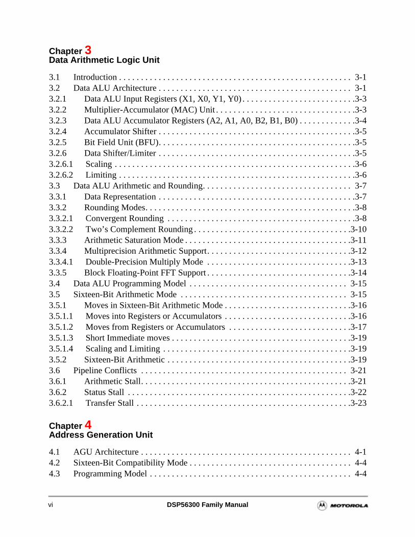
Chapter 3 Data Arithmetic Logic Unit
3.1 Introduction . . . . . . . . . . . . . . . . . . . . . . . . . . . . . . . . . . . . . . . . . . . . . . . . . . . . . 3-13.2 Data ALU Architecture . . . . . . . . . . . . . . . . . . . . . . . . . . . . . . . . . . . . . . . . . . . . 3-13.2.1 Data ALU Input Registers (X1, X0, Y1, Y0) . . . . . . . . . . . . . . . . . . . . . . . . . .3-33.2.2 Multiplier-Accumulator (MAC) Unit . . . . . . . . . . . . . . . . . . . . . . . . . . . . . . . .3-33.2.3 Data ALU Accumulator Registers (A2, A1, A0, B2, B1, B0) . . . . . . . . . . . . .3-43.2.4 Accumulator Shifter . . . . . . . . . . . . . . . . . . . . . . . . . . . . . . . . . . . . . . . . . . . . .3-53.2.5 Bit Field Unit (BFU). . . . . . . . . . . . . . . . . . . . . . . . . . . . . . . . . . . . . . . . . . . . .3-53.2.6 Data Shifter/Limiter . . . . . . . . . . . . . . . . . . . . . . . . . . . . . . . . . . . . . . . . . . . . .3-53.2.6.1 Scaling . . . . . . . . . . . . . . . . . . . . . . . . . . . . . . . . . . . . . . . . . . . . . . . . . . . . . . .3-63.2.6.2 Limiting . . . . . . . . . . . . . . . . . . . . . . . . . . . . . . . . . . . . . . . . . . . . . . . . . . . . . .3-63.3 Data ALU Arithmetic and Rounding. . . . . . . . . . . . . . . . . . . . . . . . . . . . . . . . . . 3-73.3.1 Data Representation . . . . . . . . . . . . . . . . . . . . . . . . . . . . . . . . . . . . . . . . . . . . .3-73.3.2 Rounding Modes. . . . . . . . . . . . . . . . . . . . . . . . . . . . . . . . . . . . . . . . . . . . . . . .3-83.3.2.1 Convergent Rounding . . . . . . . . . . . . . . . . . . . . . . . . . . . . . . . . . . . . . . . . . . .3-83.3.2.2 Two’s Complement Rounding . . . . . . . . . . . . . . . . . . . . . . . . . . . . . . . . . . . 3.3.3 Arithmetic Saturation Mode . . . . . . . . . . . . . . . . . . . . . . . . . . . . . . . . . . . . .3.3.4 Multiprecision Arithmetic Support. . . . . . . . . . . . . . . . . . . . . . . . . . . . . . . . .3.3.4.1 Double-Precision Multiply Mode . . . . . . . . . . . . . . . . . . . . . . . . . . . . . . . . 3.3.5 Block Floating-Point FFT Support . . . . . . . . . . . . . . . . . . . . . . . . . . . . . . . . 3.4 Data ALU Programming Model . . . . . . . . . . . . . . . . . . . . . . . . . . . . . . . . . . . . 3.5 Sixteen-Bit Arithmetic Mode . . . . . . . . . . . . . . . . . . . . . . . . . . . . . . . . . . . . . . 3.5.1 Moves in Sixteen-Bit Arithmetic Mode . . . . . . . . . . . . . . . . . . . . . . . . . . . . .3.5.1.1 Moves into Registers or Accumulators . . . . . . . . . . . . . . . . . . . . . . . . . . . .3.5.1.2 Moves from Registers or Accumulators . . . . . . . . . . . . . . . . . . . . . . . . . . .3.5.1.3 Short Immediate moves . . . . . . . . . . . . . . . . . . . . . . . . . . . . . . . . . . . . . . . 3.5.1.4 Scaling and Limiting . . . . . . . . . . . . . . . . . . . . . . . . . . . . . . . . . . . . . . . . . .3.5.2 Sixteen-Bit Arithmetic . . . . . . . . . . . . . . . . . . . . . . . . . . . . . . . . . . . . . . . . . 3.6 Pipeline Conflicts . . . . . . . . . . . . . . . . . . . . . . . . . . . . . . . . . . . . . . . . . . . . . . .3.6.1 Arithmetic Stall. . . . . . . . . . . . . . . . . . . . . . . . . . . . . . . . . . . . . . . . . . . . . . .3.6.2 Status Stall . . . . . . . . . . . . . . . . . . . . . . . . . . . . . . . . . . . . . . . . . . . . . . . . . 3.6.2.1 Transfer Stall . . . . . . . . . . . . . . . . . . . . . . . . . . . . . . . . . . . . . . . . . . . . . . .
Chapter 4 Address Generation Unit
4.1 AGU Architecture . . . . . . . . . . . . . . . . . . . . . . . . . . . . . . . . . . . . . . . . . . . . . . .4.2 Sixteen-Bit Compatibility Mode . . . . . . . . . . . . . . . . . . . . . . . . . . . . . . . . . . . . 4.3 Programming Model . . . . . . . . . . . . . . . . . . . . . . . . . . . . . . . . . . . . . . . . . . . . .
vi DSP56300 Family Manual
-12-13
. . 5-1 . 5-3 . 5-3 . 5-4. . .5-5. . .5-6 . .5-11 . .5-18. .5-18 . .5-20. .5-23. .5-23. .5-23. .5-23 .5-24 .5-24 .5-24
. 6-2 . 6-2
4.3.1 Address Register Files . . . . . . . . . . . . . . . . . . . . . . . . . . . . . . . . . . . . . . . . . . .4-54.3.2 Stack Extension Pointer . . . . . . . . . . . . . . . . . . . . . . . . . . . . . . . . . . . . . . . . . .4-54.3.3 Offset Register Files . . . . . . . . . . . . . . . . . . . . . . . . . . . . . . . . . . . . . . . . . . . . .4-54.3.4 Modifier Register Files . . . . . . . . . . . . . . . . . . . . . . . . . . . . . . . . . . . . . . . . . .4-64.4 Addressing Modes . . . . . . . . . . . . . . . . . . . . . . . . . . . . . . . . . . . . . . . . . . . . . . . 4-64.4.1 Register Direct Modes . . . . . . . . . . . . . . . . . . . . . . . . . . . . . . . . . . . . . . . . . . .4-74.4.2 Address Register Indirect Modes . . . . . . . . . . . . . . . . . . . . . . . . . . . . . . . . . . .4-74.4.3 PC-Relative Modes. . . . . . . . . . . . . . . . . . . . . . . . . . . . . . . . . . . . . . . . . . . . . .4-94.4.4 Special Address Modes. . . . . . . . . . . . . . . . . . . . . . . . . . . . . . . . . . . . . . . . . . .4-94.5 Address Modifier Types . . . . . . . . . . . . . . . . . . . . . . . . . . . . . . . . . . . . . . . . . . 4-104.5.1 Linear Modifier (Mn = $XXFFFF) . . . . . . . . . . . . . . . . . . . . . . . . . . . . . . . .4-114.5.2 Reverse-Carry Modifier (Mn = $000000) . . . . . . . . . . . . . . . . . . . . . . . . . . .4-114.5.3 Modulo Modifier (Mn = Modulus – 1). . . . . . . . . . . . . . . . . . . . . . . . . . . . . .44.5.4 Multiple Wrap-Around Modulo Modifier . . . . . . . . . . . . . . . . . . . . . . . . . . .4
Chapter 5 Program Control Unit
5.1 Overview . . . . . . . . . . . . . . . . . . . . . . . . . . . . . . . . . . . . . . . . . . . . . . . . . . . . . 5.2 PCU Hardware Architecture . . . . . . . . . . . . . . . . . . . . . . . . . . . . . . . . . . . . . . .5.3 Instruction Pipeline . . . . . . . . . . . . . . . . . . . . . . . . . . . . . . . . . . . . . . . . . . . . . .5.4 PCU Programming Model . . . . . . . . . . . . . . . . . . . . . . . . . . . . . . . . . . . . . . . . .5.4.1 Configuration and Status Registers . . . . . . . . . . . . . . . . . . . . . . . . . . . . . . 5.4.1.1 Operating Mode Register . . . . . . . . . . . . . . . . . . . . . . . . . . . . . . . . . . . . . . 5.4.1.2 Status Register (SR) . . . . . . . . . . . . . . . . . . . . . . . . . . . . . . . . . . . . . . . . . .5.4.2 Stack and Stack Extension . . . . . . . . . . . . . . . . . . . . . . . . . . . . . . . . . . . . .5.4.3 System Stack Configuration and Operation Registers . . . . . . . . . . . . . . . . 5.4.3.1 Stack Pointer (SP) Register . . . . . . . . . . . . . . . . . . . . . . . . . . . . . . . . . . . .5.4.3.2 Stack Counter (SC) Register . . . . . . . . . . . . . . . . . . . . . . . . . . . . . . . . . . . 5.4.3.3 Stack Size (SZ) Register . . . . . . . . . . . . . . . . . . . . . . . . . . . . . . . . . . . . . . 5.4.4 Program, Loop, and Exception Processing Control . . . . . . . . . . . . . . . . . . 5.4.4.1 Program Counter (PC) Register . . . . . . . . . . . . . . . . . . . . . . . . . . . . . . . . . 5.4.4.2 Loop Address (LA) Register . . . . . . . . . . . . . . . . . . . . . . . . . . . . . . . . . . . .5.4.4.3 Loop Counter (LC) Register . . . . . . . . . . . . . . . . . . . . . . . . . . . . . . . . . . . .5.4.4.4 Vector Base Address (VBA) Register . . . . . . . . . . . . . . . . . . . . . . . . . . . . .
Chapter 6 PLL and Clock Generator
6.1 PLL and Clock Signals . . . . . . . . . . . . . . . . . . . . . . . . . . . . . . . . . . . . . . . . . . .6.2 PLL Block . . . . . . . . . . . . . . . . . . . . . . . . . . . . . . . . . . . . . . . . . . . . . . . . . . . . .
DSP56300 Family Manual vii
.7-7 .7-7. .7-7. .7-9. .7-9 .7-9.7-10.7-10 .7-10. 7-11 .7-12. .7-13. .7-15. .7-15.7-17.7-20
6.2.1 Frequency Predivider . . . . . . . . . . . . . . . . . . . . . . . . . . . . . . . . . . . . . . . . . . . .6-26.2.2 Phase Detector and Charge Pump Loop Filter . . . . . . . . . . . . . . . . . . . . . . . . .6-36.2.3 Voltage Controlled Oscillator (VCO). . . . . . . . . . . . . . . . . . . . . . . . . . . . . . . .6-36.2.3.1 Divide by 2. . . . . . . . . . . . . . . . . . . . . . . . . . . . . . . . . . . . . . . . . . . . . . . . . . . .6-36.2.3.2 Frequency Divider . . . . . . . . . . . . . . . . . . . . . . . . . . . . . . . . . . . . . . . . . . . . . .6-36.2.3.3 PLL Control Elements . . . . . . . . . . . . . . . . . . . . . . . . . . . . . . . . . . . . . . . . . . .6-46.2.3.3.1 Clock Input Division . . . . . . . . . . . . . . . . . . . . . . . . . . . . . . . . . . . . . . . . .6-46.2.3.3.2 Frequency Multiplication . . . . . . . . . . . . . . . . . . . . . . . . . . . . . . . . . . . . . .6-46.2.3.3.3 Skew Elimination . . . . . . . . . . . . . . . . . . . . . . . . . . . . . . . . . . . . . . . . . . . .6-46.2.3.4 Clock Generator . . . . . . . . . . . . . . . . . . . . . . . . . . . . . . . . . . . . . . . . . . . . . . . .6-56.2.3.4.1 Low-Power Divider (LPD). . . . . . . . . . . . . . . . . . . . . . . . . . . . . . . . . . . . .6-56.2.3.4.2 Internal and External Clock Pulse Generator . . . . . . . . . . . . . . . . . . . . . . .6-56.2.3.4.3 Operating Frequency . . . . . . . . . . . . . . . . . . . . . . . . . . . . . . . . . . . . . . . . .6-66.3 PLL Programming Model . . . . . . . . . . . . . . . . . . . . . . . . . . . . . . . . . . . . . . . . . . 6-66.4 Clock Synchronization . . . . . . . . . . . . . . . . . . . . . . . . . . . . . . . . . . . . . . . . . . . 6-106.5 Design Guidelines for Ripple and PCAP . . . . . . . . . . . . . . . . . . . . . . . . . . . . . 6-10
Chapter 7 Debugging Support
7.1 JTAG Test Access Port . . . . . . . . . . . . . . . . . . . . . . . . . . . . . . . . . . . . . . . . . . . . 7-27.1.1 Boundary Scan Architecture Overview . . . . . . . . . . . . . . . . . . . . . . . . . . . . . .7-27.1.2 TAP Controller . . . . . . . . . . . . . . . . . . . . . . . . . . . . . . . . . . . . . . . . . . . . . . . . .7-37.1.3 Boundary Scan Register . . . . . . . . . . . . . . . . . . . . . . . . . . . . . . . . . . . . . . . . . .7-57.1.4 Instruction Register. . . . . . . . . . . . . . . . . . . . . . . . . . . . . . . . . . . . . . . . . . . . . .7-57.1.4.1 EXTEST (B[3–0] = 0000) . . . . . . . . . . . . . . . . . . . . . . . . . . . . . . . . . . . . . . .7.1.4.2 SAMPLE/PRELOAD (B[3–0] = 0001) . . . . . . . . . . . . . . . . . . . . . . . . . . . . .7.1.4.3 IDCODE (B[3–0] = 0010) . . . . . . . . . . . . . . . . . . . . . . . . . . . . . . . . . . . . . . 7.1.4.4 CLAMP (B[3–0] = 0011). . . . . . . . . . . . . . . . . . . . . . . . . . . . . . . . . . . . . . . 7.1.4.5 HI-Z (B[3–0] = 0100) . . . . . . . . . . . . . . . . . . . . . . . . . . . . . . . . . . . . . . . . . 7.1.4.6 ENABLE_ONCE(B[3–0] = 0110). . . . . . . . . . . . . . . . . . . . . . . . . . . . . . . . .7.1.4.7 DEBUG_REQUEST(B[3–0] = 0111) . . . . . . . . . . . . . . . . . . . . . . . . . . . . . 7.1.4.8 BYPASS (B[3–0] = 1111) . . . . . . . . . . . . . . . . . . . . . . . . . . . . . . . . . . . . . . 7.1.5 DSP56300 JTAG Restrictions . . . . . . . . . . . . . . . . . . . . . . . . . . . . . . . . . . .7.2 OnCE Module . . . . . . . . . . . . . . . . . . . . . . . . . . . . . . . . . . . . . . . . . . . . . . . . . 7.2.1 OnCE Controller. . . . . . . . . . . . . . . . . . . . . . . . . . . . . . . . . . . . . . . . . . . . . .7.2.1.1 OnCE Command Register (OCR) . . . . . . . . . . . . . . . . . . . . . . . . . . . . . . . 7.2.1.2 OnCE Decoder (ODEC). . . . . . . . . . . . . . . . . . . . . . . . . . . . . . . . . . . . . . . 7.2.1.3 OnCE Status and Control Register (OSCR) . . . . . . . . . . . . . . . . . . . . . . . 7.2.2 OnCE Memory Breakpoint Logic . . . . . . . . . . . . . . . . . . . . . . . . . . . . . . . . 7.2.2.1 OnCE Memory Breakpoint Counter (OMBC). . . . . . . . . . . . . . . . . . . . . . .
viii DSP56300 Family Manual
7.2.3 Cache Support. . . . . . . . . . . . . . . . . . . . . . . . . . . . . . . . . . . . . . . . . . . . . . . . .7-207.2.3.1 OnCE Trace Logic . . . . . . . . . . . . . . . . . . . . . . . . . . . . . . . . . . . . . . . . . . . . .7-227.2.4 Methods of Entering Debug Mode . . . . . . . . . . . . . . . . . . . . . . . . . . . . . . . . .7-237.2.5 Trace Buffer . . . . . . . . . . . . . . . . . . . . . . . . . . . . . . . . . . . . . . . . . . . . . . . . . .7-257.2.6 OnCE Commands and Serial Protocol . . . . . . . . . . . . . . . . . . . . . . . . . . . . . .7-267.2.7 OnCE Module Examples . . . . . . . . . . . . . . . . . . . . . . . . . . . . . . . . . . . . . . . .7-287.2.7.1 Checking Whether the Chip Has Entered Debug Mode . . . . . . . . . . . . . . . .7-287.2.7.2 Polling the JTAG Instruction Register. . . . . . . . . . . . . . . . . . . . . . . . . . . . . .7-297.2.7.3 Saving Pipeline Information . . . . . . . . . . . . . . . . . . . . . . . . . . . . . . . . . . . . .7-297.2.7.4 Reading the Trace Buffer . . . . . . . . . . . . . . . . . . . . . . . . . . . . . . . . . . . . . . . .7-297.2.7.5 Displaying a Specified Register . . . . . . . . . . . . . . . . . . . . . . . . . . . . . . . . . . .7-307.2.7.6 Displaying X Memory Area Starting at Address $xxxxxx . . . . . . . . . . . . . .7-307.2.7.7 Returning From Debug Mode to Normal Mode to Current Program . . . . . .7-327.2.7.8 Returning from Debug Mode to Normal Mode to a New Program . . . . . . . .7-327.3 Examples of JTAG-OnCE Interaction. . . . . . . . . . . . . . . . . . . . . . . . . . . . . . . . 7-337.3.1 Address Trace Mode. . . . . . . . . . . . . . . . . . . . . . . . . . . . . . . . . . . . . . . . . . . .7-36
Chapter 8 Instruction Cache
8.1 Instruction Cache Architecture . . . . . . . . . . . . . . . . . . . . . . . . . . . . . . . . . . . . . . 8-28.2 Cache Programming Model. . . . . . . . . . . . . . . . . . . . . . . . . . . . . . . . . . . . . . . . . 8-38.2.1 Cache Operation . . . . . . . . . . . . . . . . . . . . . . . . . . . . . . . . . . . . . . . . . . . . . . . .8-48.2.1.1 Program Fetch . . . . . . . . . . . . . . . . . . . . . . . . . . . . . . . . . . . . . . . . . . . . . . . . .8-48.2.1.2 Cache Hit . . . . . . . . . . . . . . . . . . . . . . . . . . . . . . . . . . . . . . . . . . . . . . . . . . . . .8-48.2.1.3 Cache Word Miss When Burst Mode Is Disabled . . . . . . . . . . . . . . . . . . . . . .8-48.2.1.4 Cache Word Miss When Burst Mode Is Enabled . . . . . . . . . . . . . . . . . . . . . .8-58.2.1.5 Sector Miss. . . . . . . . . . . . . . . . . . . . . . . . . . . . . . . . . . . . . . . . . . . . . . . . . . . .8-58.2.2 Default Mode After Hardware Reset . . . . . . . . . . . . . . . . . . . . . . . . . . . . . . . .8-68.3 Cache Locking. . . . . . . . . . . . . . . . . . . . . . . . . . . . . . . . . . . . . . . . . . . . . . . . . . . 8-68.4 Cache Unlocking . . . . . . . . . . . . . . . . . . . . . . . . . . . . . . . . . . . . . . . . . . . . . . . . . 8-68.5 Flushing the Cache . . . . . . . . . . . . . . . . . . . . . . . . . . . . . . . . . . . . . . . . . . . . . . . 8-78.6 Data Transfers to/from Instruction Cache . . . . . . . . . . . . . . . . . . . . . . . . . . . . . . 8-88.6.1 DMA Transfers. . . . . . . . . . . . . . . . . . . . . . . . . . . . . . . . . . . . . . . . . . . . . . . . .8-88.6.2 Software-Controlled Transfers . . . . . . . . . . . . . . . . . . . . . . . . . . . . . . . . . . . . .8-88.7 Using the Instruction Cache in Real-Time Applications. . . . . . . . . . . . . . . . . . . 8-98.8 Debugging Instruction Cache Operation . . . . . . . . . . . . . . . . . . . . . . . . . . . . . . 8-10
DSP56300 Family Manual ix
.9-14. .9-14 .9-14. .9-149-14. .9-15 9-15.9-15. .9-19.9-21
10-3. .10-3 . .10-4. .10-4. .10-5. .10-5 10-6 .10-6 .10-7. 10-7.10-7
Chapter 9 External Memory Interface (Port A)
9.1 Signal Description . . . . . . . . . . . . . . . . . . . . . . . . . . . . . . . . . . . . . . . . . . . . . . . . 9-19.2 Port Operation . . . . . . . . . . . . . . . . . . . . . . . . . . . . . . . . . . . . . . . . . . . . . . . . . . . 9-59.2.1 External Memory Addressing. . . . . . . . . . . . . . . . . . . . . . . . . . . . . . . . . . . . . .9-59.2.2 SRAM Support . . . . . . . . . . . . . . . . . . . . . . . . . . . . . . . . . . . . . . . . . . . . . . . . .9-69.2.3 DRAM Support. . . . . . . . . . . . . . . . . . . . . . . . . . . . . . . . . . . . . . . . . . . . . . . . .9-89.2.3.1 DRAM In-Page Access . . . . . . . . . . . . . . . . . . . . . . . . . . . . . . . . . . . . . . . . .9-109.2.3.2 DRAM Out-of-Page Access. . . . . . . . . . . . . . . . . . . . . . . . . . . . . . . . . . . . . .9-109.3 Port A Disable . . . . . . . . . . . . . . . . . . . . . . . . . . . . . . . . . . . . . . . . . . . . . . . . . . 9-119.4 Bus Handshake and Arbitration. . . . . . . . . . . . . . . . . . . . . . . . . . . . . . . . . . . . . 9-119.5 Bus Arbitration Signals . . . . . . . . . . . . . . . . . . . . . . . . . . . . . . . . . . . . . . . . . . . 9-119.5.1 The Arbitration Protocol. . . . . . . . . . . . . . . . . . . . . . . . . . . . . . . . . . . . . . . . .9-129.5.2 Arbitration Scheme. . . . . . . . . . . . . . . . . . . . . . . . . . . . . . . . . . . . . . . . . . . . .9-139.5.3 Bus Arbitration Example Cases . . . . . . . . . . . . . . . . . . . . . . . . . . . . . . . . . . .9-149.5.3.1 Case 1—Normal. . . . . . . . . . . . . . . . . . . . . . . . . . . . . . . . . . . . . . . . . . . . . .9.5.3.2 Case 2—Bus Busy . . . . . . . . . . . . . . . . . . . . . . . . . . . . . . . . . . . . . . . . . . . 9.5.3.3 Case 3—Low Priority . . . . . . . . . . . . . . . . . . . . . . . . . . . . . . . . . . . . . . . . .9.5.3.4 Case 4—Default . . . . . . . . . . . . . . . . . . . . . . . . . . . . . . . . . . . . . . . . . . . . . 9.5.3.5 Case 5—Bus Lock during Read-Modify-Write Instructions . . . . . . . . . . . . .9.5.3.6 Case 6—Bus Parking . . . . . . . . . . . . . . . . . . . . . . . . . . . . . . . . . . . . . . . . . 9.6 Port A Control . . . . . . . . . . . . . . . . . . . . . . . . . . . . . . . . . . . . . . . . . . . . . . . . . .9.6.1 Address Attribute Registers (AAR[0–3]) . . . . . . . . . . . . . . . . . . . . . . . . . . . 9.6.2 Bus Control Register. . . . . . . . . . . . . . . . . . . . . . . . . . . . . . . . . . . . . . . . . . 9.6.3 DRAM Control Register. . . . . . . . . . . . . . . . . . . . . . . . . . . . . . . . . . . . . . . .
Chapter 10 DMA Controller
10.1 DMA Operational Overview . . . . . . . . . . . . . . . . . . . . . . . . . . . . . . . . . . . . . . . 10.1.1 Basic Address Modes . . . . . . . . . . . . . . . . . . . . . . . . . . . . . . . . . . . . . . . . . 10.1.2 Special Address Modes. . . . . . . . . . . . . . . . . . . . . . . . . . . . . . . . . . . . . . . .10.1.3 Unmatched Source and Destination Dimensions . . . . . . . . . . . . . . . . . . . . 10.1.4 DMA Triggers (Request Sources) . . . . . . . . . . . . . . . . . . . . . . . . . . . . . . . 10.1.5 Transfer Mode . . . . . . . . . . . . . . . . . . . . . . . . . . . . . . . . . . . . . . . . . . . . . . 10.2 Timing (Core Clock Cycles) . . . . . . . . . . . . . . . . . . . . . . . . . . . . . . . . . . . . . . .10.2.1 Non-Overlap Between DMA Channels . . . . . . . . . . . . . . . . . . . . . . . . . . . .10.2.2 Overlap between DMA Channel and Core. . . . . . . . . . . . . . . . . . . . . . . . . .10.3 Channel Priority. . . . . . . . . . . . . . . . . . . . . . . . . . . . . . . . . . . . . . . . . . . . . . . . 10.3.1 Priority Between DMA Channels. . . . . . . . . . . . . . . . . . . . . . . . . . . . . . . . .
x DSP56300 Family Manual
00-100-100-110-120-130-140-150-160-21
10-220-2410-2410-26
11-2. .11-3. .11-311-5 .11-5 .11-5 .11-5. .11-6 .11-6.11-6 .11-6 .11-6 .11-7. .11-7. .11-7 . .11-7. .11-8
10.3.2 Priority Between a DMA Channel and the Core . . . . . . . . . . . . . . . . . . . . . .10-810.4 Special Uses of DMA With the Bus Interface Unit. . . . . . . . . . . . . . . . . . . . . . 10-910.4.1 Byte Packing. . . . . . . . . . . . . . . . . . . . . . . . . . . . . . . . . . . . . . . . . . . . . . . . . .10-910.4.1.1 DRAM In-Page Accesses using DMA. . . . . . . . . . . . . . . . . . . . . . . . . . . . . .10-910.4.1.2 End-of-Block-Transfer Interrupt . . . . . . . . . . . . . . . . . . . . . . . . . . . . . . . . . .10-910.5 DMA Controller Programming Model . . . . . . . . . . . . . . . . . . . . . . . . . . . . . . 10-1010.5.1 DMA Source Address Registers (DSR[0–5]). . . . . . . . . . . . . . . . . . . . . . . .10-110.5.2 DMA Destination Address Registers (DDR[5–0]). . . . . . . . . . . . . . . . . . . .110.5.3 DMA Counters (DCO[5–0]). . . . . . . . . . . . . . . . . . . . . . . . . . . . . . . . . . . . .110.5.3.1 DMA Counter Mode A—Single Counter . . . . . . . . . . . . . . . . . . . . . . . . . .110.5.3.2 DMA Counter Mode B—Dual Counter. . . . . . . . . . . . . . . . . . . . . . . . . . . .110.5.3.3 Circular Buffer (Length Less Than or Equal to 4096 Words) . . . . . . . . . . .110.5.3.3.1 DMA Counter Modes C, D and E—Triple Counter. . . . . . . . . . . . . . . .110.5.3.4 Circular Buffer (Length Greater Than 4096 Words) . . . . . . . . . . . . . . . . . .110.5.3.5 DMA Control Registers (DCR[5–0]). . . . . . . . . . . . . . . . . . . . . . . . . . . . . .110.5.3.5.1 Non-3D Addressing Modes (D3D = 0) . . . . . . . . . . . . . . . . . . . . . . . . .110.5.3.5.2 3D Modes (D3D = 1) . . . . . . . . . . . . . . . . . . . . . . . . . . . . . . . . . . . . . . .10.5.3.6 DMA Offset Registers (DOR[3–0]). . . . . . . . . . . . . . . . . . . . . . . . . . . . . . .110.5.3.7 DMA Status Register (DSTR) . . . . . . . . . . . . . . . . . . . . . . . . . . . . . . . . . . .10.6 DMA Restrictions . . . . . . . . . . . . . . . . . . . . . . . . . . . . . . . . . . . . . . . . . . . . . .
Chapter 11 Operating Modes and Memory Spaces
11.1 DSP56300 Family Core Memory Map . . . . . . . . . . . . . . . . . . . . . . . . . . . . . . .11.1.1 X Data Memory Space . . . . . . . . . . . . . . . . . . . . . . . . . . . . . . . . . . . . . . . . 11.1.2 Internal X I/O Space . . . . . . . . . . . . . . . . . . . . . . . . . . . . . . . . . . . . . . . . . . 11.1.3 Switchable Internal or External X I/O Memory . . . . . . . . . . . . . . . . . . . . . . .11.1.3.1 Reserved Space for X ROM or RAM . . . . . . . . . . . . . . . . . . . . . . . . . . . . .11.1.3.2 External X Data Memory. . . . . . . . . . . . . . . . . . . . . . . . . . . . . . . . . . . . . . .11.1.3.3 Internal X Memory. . . . . . . . . . . . . . . . . . . . . . . . . . . . . . . . . . . . . . . . . . . .11.1.4 Y Data Memory Space . . . . . . . . . . . . . . . . . . . . . . . . . . . . . . . . . . . . . . . . 11.1.4.1 Internal/External Y I/O Space . . . . . . . . . . . . . . . . . . . . . . . . . . . . . . . . . . .11.1.4.2 Switchable Internal or External Y I/O Memory. . . . . . . . . . . . . . . . . . . . . . 11.1.4.3 Reserved Space for Y ROM or RAM . . . . . . . . . . . . . . . . . . . . . . . . . . . . .11.1.4.4 External Y Data Memory. . . . . . . . . . . . . . . . . . . . . . . . . . . . . . . . . . . . . . .11.1.4.5 Internal Y Memory. . . . . . . . . . . . . . . . . . . . . . . . . . . . . . . . . . . . . . . . . . . .11.1.5 Program Memory . . . . . . . . . . . . . . . . . . . . . . . . . . . . . . . . . . . . . . . . . . . . 11.1.5.1 Bootstrap ROM Space . . . . . . . . . . . . . . . . . . . . . . . . . . . . . . . . . . . . . . . . 11.1.5.2 Reserved Space for Program ROM . . . . . . . . . . . . . . . . . . . . . . . . . . . . . .11.1.5.3 External Program Memory. . . . . . . . . . . . . . . . . . . . . . . . . . . . . . . . . . . . .
DSP56300 Family Manual xi
11.1.5.4 Internal Program Memory . . . . . . . . . . . . . . . . . . . . . . . . . . . . . . . . . . . . . . .11-811.1.5.5 Internal Instruction Cache RAM . . . . . . . . . . . . . . . . . . . . . . . . . . . . . . . . . .11-811.2 Sixteen-Bit Compatibility Mode . . . . . . . . . . . . . . . . . . . . . . . . . . . . . . . . . . . . 11-811.3 Memory Switch Mode . . . . . . . . . . . . . . . . . . . . . . . . . . . . . . . . . . . . . . . . . . . . 11-9
Chapter 12 Guide to the Instruction Set
12.1 Instruction Formats and Syntax. . . . . . . . . . . . . . . . . . . . . . . . . . . . . . . . . . . . . 12-112.2 Operand Lengths . . . . . . . . . . . . . . . . . . . . . . . . . . . . . . . . . . . . . . . . . . . . . . . . 12-312.2.1 Data ALU Registers . . . . . . . . . . . . . . . . . . . . . . . . . . . . . . . . . . . . . . . . . . . .12-412.2.2 AGU Registers . . . . . . . . . . . . . . . . . . . . . . . . . . . . . . . . . . . . . . . . . . . . . . . .12-512.2.3 Program Control Registers . . . . . . . . . . . . . . . . . . . . . . . . . . . . . . . . . . . . . . .12-512.2.4 Data Organization in Memory . . . . . . . . . . . . . . . . . . . . . . . . . . . . . . . . . . . .12-612.3 Instruction Groups . . . . . . . . . . . . . . . . . . . . . . . . . . . . . . . . . . . . . . . . . . . . . . . 12-712.3.1 Arithmetic Instructions . . . . . . . . . . . . . . . . . . . . . . . . . . . . . . . . . . . . . . . . . .12-712.3.2 Logical Instructions . . . . . . . . . . . . . . . . . . . . . . . . . . . . . . . . . . . . . . . . . . . .12-912.3.3 Bit Manipulation Instructions . . . . . . . . . . . . . . . . . . . . . . . . . . . . . . . . . . . .12-1112.3.4 Loop Instructions . . . . . . . . . . . . . . . . . . . . . . . . . . . . . . . . . . . . . . . . . . . . .12-1112.3.5 Move Instructions . . . . . . . . . . . . . . . . . . . . . . . . . . . . . . . . . . . . . . . . . . . . .12-1212.3.6 Program Control Instructions . . . . . . . . . . . . . . . . . . . . . . . . . . . . . . . . . . . .12-1312.3.7 Instruction Cache Control Instructions. . . . . . . . . . . . . . . . . . . . . . . . . . . . .12-1412.4 Guide to Instruction Descriptions . . . . . . . . . . . . . . . . . . . . . . . . . . . . . . . . . . 12-1512.4.1 Notation . . . . . . . . . . . . . . . . . . . . . . . . . . . . . . . . . . . . . . . . . . . . . . . . . . . .12-1512.4.2 Condition Code Computation . . . . . . . . . . . . . . . . . . . . . . . . . . . . . . . . . . . .12-2012.5 Instruction Partial Encoding . . . . . . . . . . . . . . . . . . . . . . . . . . . . . . . . . . . . . . 12-2112.5.1 Partial Encodings for Use in Instruction Encoding . . . . . . . . . . . . . . . . . . .12-2112.5.2 Parallel Instruction Encoding of the Operation Code. . . . . . . . . . . . . . . . . .12-2812.5.2.1 Multiply Instruction Encoding . . . . . . . . . . . . . . . . . . . . . . . . . . . . . . . . . . .12-2812.5.2.2 Non-Multiply Instruction Encoding. . . . . . . . . . . . . . . . . . . . . . . . . . . . . . .12-29
Chapter 13 Instruction Set
Appendix A Instruction Timing and Restrictions
A.1 Overview . . . . . . . . . . . . . . . . . . . . . . . . . . . . . . . . . . . . . . . . . . . . . . . . . . . . . . . A-1A.2 Instruction Sequence Delays . . . . . . . . . . . . . . . . . . . . . . . . . . . . . . . . . . . . . . . A-10A.2.1 External Bus Wait States . . . . . . . . . . . . . . . . . . . . . . . . . . . . . . . . . . . . . . . A-10A.2.2 Instruction Fetch Delays . . . . . . . . . . . . . . . . . . . . . . . . . . . . . . . . . . . . . . . . A-11
xii DSP56300 Family Manual
-15-15
A-15 A-16. A-16 A-16. A-16 A-16 A-19 A-23 A-23 A-24 A-24. A-25. A-25 A-26. A-27 A-27A-28A-28A-29-29
. . B-3
. B-3
. B-4. . B-5. . B-6 B-7B-8B-10B-11. B-12. B-13
A.2.3 Data ALU Interlock . . . . . . . . . . . . . . . . . . . . . . . . . . . . . . . . . . . . . . . . . . . A-11A.2.4 Address Register Interlocks . . . . . . . . . . . . . . . . . . . . . . . . . . . . . . . . . . . . . A-11A.2.5 Stack Extension Delays . . . . . . . . . . . . . . . . . . . . . . . . . . . . . . . . . . . . . . . . A-13A.2.6 Program Flow Control Delays . . . . . . . . . . . . . . . . . . . . . . . . . . . . . . . . . . . A-15A.2.6.1 JMP to LA or to LA – 1 . . . . . . . . . . . . . . . . . . . . . . . . . . . . . . . . . . . . . . . . AA.2.6.2 RTI to LA or to LA – 1 . . . . . . . . . . . . . . . . . . . . . . . . . . . . . . . . . . . . . . . . AA.2.6.3 Conditional Instructions. . . . . . . . . . . . . . . . . . . . . . . . . . . . . . . . . . . . . . . .A.2.6.4 Interrupt Abort . . . . . . . . . . . . . . . . . . . . . . . . . . . . . . . . . . . . . . . . . . . . . . .A.2.6.5 Degenerated DO loop. . . . . . . . . . . . . . . . . . . . . . . . . . . . . . . . . . . . . . . . . A.2.6.6 Annulled REP and DO. . . . . . . . . . . . . . . . . . . . . . . . . . . . . . . . . . . . . . . . .A.3 Instruction Sequence Restrictions . . . . . . . . . . . . . . . . . . . . . . . . . . . . . . . . . . A.3.1 Restrictions Near the End of DO Loops. . . . . . . . . . . . . . . . . . . . . . . . . . . .A.3.2 General DO Restrictions. . . . . . . . . . . . . . . . . . . . . . . . . . . . . . . . . . . . . . . .A.3.3 ENDDO Restrictions . . . . . . . . . . . . . . . . . . . . . . . . . . . . . . . . . . . . . . . . . .A.3.4 BRKcc Restrictions . . . . . . . . . . . . . . . . . . . . . . . . . . . . . . . . . . . . . . . . . . .A.3.5 RTI and RTS Restrictions. . . . . . . . . . . . . . . . . . . . . . . . . . . . . . . . . . . . . . .A.3.6 SP/SC and SSH/SSL Manipulation Restrictions . . . . . . . . . . . . . . . . . . . . .A.3.7 Fast Interrupt Routines . . . . . . . . . . . . . . . . . . . . . . . . . . . . . . . . . . . . . . . . A.3.8 REP Restrictions. . . . . . . . . . . . . . . . . . . . . . . . . . . . . . . . . . . . . . . . . . . . . A.3.9 Stack Extension Restrictions . . . . . . . . . . . . . . . . . . . . . . . . . . . . . . . . . . . .A.3.10 Stack Extension Enable Restrictions . . . . . . . . . . . . . . . . . . . . . . . . . . . . . A.4 Peripheral Pipeline Restrictions. . . . . . . . . . . . . . . . . . . . . . . . . . . . . . . . . . . . .A.4.1 Polling a Peripheral Device for Write . . . . . . . . . . . . . . . . . . . . . . . . . . . . . A.4.2 Writing to a Read-Only Register . . . . . . . . . . . . . . . . . . . . . . . . . . . . . . . . . A.4.3 XY Memory Data Move. . . . . . . . . . . . . . . . . . . . . . . . . . . . . . . . . . . . . . . . A.5 Sixteen-Bit Compatibility Mode Restrictions . . . . . . . . . . . . . . . . . . . . . . . . . . A
Appendix B Benchmark Programs
B.1 Benchmarks . . . . . . . . . . . . . . . . . . . . . . . . . . . . . . . . . . . . . . . . . . . . . . . . . . . B.1.1 Real Multiply . . . . . . . . . . . . . . . . . . . . . . . . . . . . . . . . . . . . . . . . . . . . . . . . B.1.2 N Real Multiplies . . . . . . . . . . . . . . . . . . . . . . . . . . . . . . . . . . . . . . . . . . . . . B.1.3 Real Update . . . . . . . . . . . . . . . . . . . . . . . . . . . . . . . . . . . . . . . . . . . . . . . . B.1.4 N Real Updates . . . . . . . . . . . . . . . . . . . . . . . . . . . . . . . . . . . . . . . . . . . . . . B.1.5 Real Correlation or Convolution (FIR Filter). . . . . . . . . . . . . . . . . . . . . . . . .B.1.6 Real * Complex Correlation or Convolution (FIR Filter) . . . . . . . . . . . . . . . B.1.7 Complex Multiply. . . . . . . . . . . . . . . . . . . . . . . . . . . . . . . . . . . . . . . . . . . . . B.1.8 N Complex Multiplies . . . . . . . . . . . . . . . . . . . . . . . . . . . . . . . . . . . . . . . . . B.1.9 Complex Update . . . . . . . . . . . . . . . . . . . . . . . . . . . . . . . . . . . . . . . . . . . . . B.1.10 N Complex Updates . . . . . . . . . . . . . . . . . . . . . . . . . . . . . . . . . . . . . . . . . .
DSP56300 Family Manual xiii
B.1.11 Complex Correlation or Convolution (FIR Filter) . . . . . . . . . . . . . . . . . . . . B-15B.1.12 Nth Order Power Series (Real) . . . . . . . . . . . . . . . . . . . . . . . . . . . . . . . . . . . B-17B.1.13 Second Order Real Biquad IIR Filter . . . . . . . . . . . . . . . . . . . . . . . . . . . . . . B-18B.1.14 N Cascaded Real Biquad IIR Filter . . . . . . . . . . . . . . . . . . . . . . . . . . . . . . . B-19B.1.15 N Radix-2 FFT Butterflies (DIT, In-Place Algorithm) . . . . . . . . . . . . . . . . B-20B.1.16 True (Exact) LMS Adaptive Filter . . . . . . . . . . . . . . . . . . . . . . . . . . . . . . . . B-21B.1.17 Delayed LMS Adaptive Filter . . . . . . . . . . . . . . . . . . . . . . . . . . . . . . . . . . . B-24B.1.18 FIR Lattice Filter . . . . . . . . . . . . . . . . . . . . . . . . . . . . . . . . . . . . . . . . . . . . . B-26B.1.19 All Pole IIR Lattice Filter . . . . . . . . . . . . . . . . . . . . . . . . . . . . . . . . . . . . . . . B-28B.1.20 General Lattice Filter . . . . . . . . . . . . . . . . . . . . . . . . . . . . . . . . . . . . . . . . . . B-30B.1.21 Normalized Lattice Filter . . . . . . . . . . . . . . . . . . . . . . . . . . . . . . . . . . . . . . . B-32B.1.22 [1 × 3][3 × 3] Matrix Multiplication. . . . . . . . . . . . . . . . . . . . . . . . . . . . . . . B-34B.1.23 N Point 3 × 3 2-D FIR Convolution . . . . . . . . . . . . . . . . . . . . . . . . . . . . . . . B-35B.1.24 Viterbi Add-Compare-Select (ACS). . . . . . . . . . . . . . . . . . . . . . . . . . . . . . . B-38B.1.25 Parsing a Data Stream. . . . . . . . . . . . . . . . . . . . . . . . . . . . . . . . . . . . . . . . . . B-41B.1.26 Creating a Data Stream. . . . . . . . . . . . . . . . . . . . . . . . . . . . . . . . . . . . . . . . . B-43B.1.27 Parsing a Hoffman Code Data Stream . . . . . . . . . . . . . . . . . . . . . . . . . . . . . B-45
Appendix C From CDR Process to HiP Process
C.1 Voltage. . . . . . . . . . . . . . . . . . . . . . . . . . . . . . . . . . . . . . . . . . . . . . . . . . . . . . . . . C-2C.2 Operating Frequency . . . . . . . . . . . . . . . . . . . . . . . . . . . . . . . . . . . . . . . . . . . . . . C-2C.3 Port A Timings . . . . . . . . . . . . . . . . . . . . . . . . . . . . . . . . . . . . . . . . . . . . . . . . . . C-2C.4 Memory Block Size . . . . . . . . . . . . . . . . . . . . . . . . . . . . . . . . . . . . . . . . . . . . . . . C-3
xiv DSP56300 Family Manual
Figures
3-10
3-12
13
-14
3-15
3-16
-21
3-22
3-23
. 4-2
. 4-4
. 5-3
. . 5-4
. 5-5
. 5-6
. 5-11
. 5-20
. 6-1
. 6-2
. 6-5
. 6-6
6-11
. 7-4
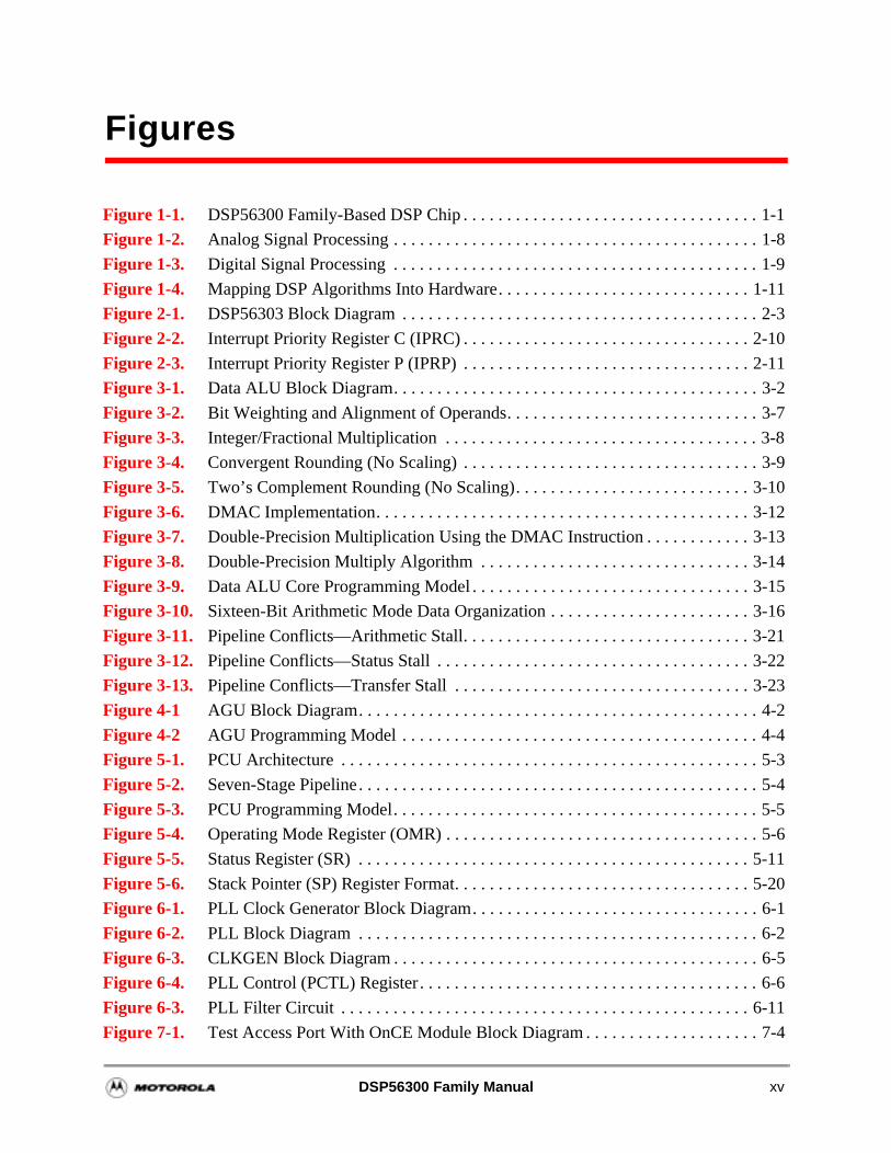
Figure 1-1. DSP56300 Family-Based DSP Chip . . . . . . . . . . . . . . . . . . . . . . . . . . . . . . . . . . 1-1
Figure 1-2. Analog Signal Processing . . . . . . . . . . . . . . . . . . . . . . . . . . . . . . . . . . . . . . . . . . 1-8
Figure 1-3. Digital Signal Processing . . . . . . . . . . . . . . . . . . . . . . . . . . . . . . . . . . . . . . . . . . 1-9
Figure 1-4. Mapping DSP Algorithms Into Hardware. . . . . . . . . . . . . . . . . . . . . . . . . . . . . 1-11
Figure 2-1. DSP56303 Block Diagram . . . . . . . . . . . . . . . . . . . . . . . . . . . . . . . . . . . . . . . . . 2-3
Figure 2-2. Interrupt Priority Register C (IPRC) . . . . . . . . . . . . . . . . . . . . . . . . . . . . . . . . . 2-10
Figure 2-3. Interrupt Priority Register P (IPRP) . . . . . . . . . . . . . . . . . . . . . . . . . . . . . . . . . 2-11
Figure 3-1. Data ALU Block Diagram. . . . . . . . . . . . . . . . . . . . . . . . . . . . . . . . . . . . . . . . . . 3-2
Figure 3-2. Bit Weighting and Alignment of Operands. . . . . . . . . . . . . . . . . . . . . . . . . . . . . 3-7
Figure 3-3. Integer/Fractional Multiplication . . . . . . . . . . . . . . . . . . . . . . . . . . . . . . . . . . . . 3-8
Figure 3-4. Convergent Rounding (No Scaling) . . . . . . . . . . . . . . . . . . . . . . . . . . . . . . . . . . 3-9
Figure 3-5. Two’s Complement Rounding (No Scaling). . . . . . . . . . . . . . . . . . . . . . . . . . .
Figure 3-6. DMAC Implementation. . . . . . . . . . . . . . . . . . . . . . . . . . . . . . . . . . . . . . . . . . .
Figure 3-7. Double-Precision Multiplication Using the DMAC Instruction . . . . . . . . . . . . 3-
Figure 3-8. Double-Precision Multiply Algorithm . . . . . . . . . . . . . . . . . . . . . . . . . . . . . . . 3
Figure 3-9. Data ALU Core Programming Model . . . . . . . . . . . . . . . . . . . . . . . . . . . . . . . .
Figure 3-10. Sixteen-Bit Arithmetic Mode Data Organization . . . . . . . . . . . . . . . . . . . . . . .
Figure 3-11. Pipeline Conflicts—Arithmetic Stall. . . . . . . . . . . . . . . . . . . . . . . . . . . . . . . . . 3
Figure 3-12. Pipeline Conflicts—Status Stall . . . . . . . . . . . . . . . . . . . . . . . . . . . . . . . . . . . .
Figure 3-13. Pipeline Conflicts—Transfer Stall . . . . . . . . . . . . . . . . . . . . . . . . . . . . . . . . . .
Figure 4-1 AGU Block Diagram. . . . . . . . . . . . . . . . . . . . . . . . . . . . . . . . . . . . . . . . . . . . .
Figure 4-2 AGU Programming Model . . . . . . . . . . . . . . . . . . . . . . . . . . . . . . . . . . . . . . . .
Figure 5-1. PCU Architecture . . . . . . . . . . . . . . . . . . . . . . . . . . . . . . . . . . . . . . . . . . . . . . .
Figure 5-2. Seven-Stage Pipeline. . . . . . . . . . . . . . . . . . . . . . . . . . . . . . . . . . . . . . . . . . . .
Figure 5-3. PCU Programming Model. . . . . . . . . . . . . . . . . . . . . . . . . . . . . . . . . . . . . . . . .
Figure 5-4. Operating Mode Register (OMR) . . . . . . . . . . . . . . . . . . . . . . . . . . . . . . . . . . .
Figure 5-5. Status Register (SR) . . . . . . . . . . . . . . . . . . . . . . . . . . . . . . . . . . . . . . . . . . . .
Figure 5-6. Stack Pointer (SP) Register Format. . . . . . . . . . . . . . . . . . . . . . . . . . . . . . . . .
Figure 6-1. PLL Clock Generator Block Diagram. . . . . . . . . . . . . . . . . . . . . . . . . . . . . . . .
Figure 6-2. PLL Block Diagram . . . . . . . . . . . . . . . . . . . . . . . . . . . . . . . . . . . . . . . . . . . . .
Figure 6-3. CLKGEN Block Diagram . . . . . . . . . . . . . . . . . . . . . . . . . . . . . . . . . . . . . . . . .
Figure 6-4. PLL Control (PCTL) Register. . . . . . . . . . . . . . . . . . . . . . . . . . . . . . . . . . . . . .
Figure 6-3. PLL Filter Circuit . . . . . . . . . . . . . . . . . . . . . . . . . . . . . . . . . . . . . . . . . . . . . . .
Figure 7-1. Test Access Port With OnCE Module Block Diagram . . . . . . . . . . . . . . . . . . .
DSP56300 Family Manual xv
9-16
9-19
9-21
-11
0-11
0-12
0-14
0-16
0-24
11-2
11-9
12-1
. 12-3
12-3
12-5
12-6
Figure 7-2. TAP Controller State Machine . . . . . . . . . . . . . . . . . . . . . . . . . . . . . . . . . . . . . . 7-5
Figure 7-3. JTAG Instruction Register Format . . . . . . . . . . . . . . . . . . . . . . . . . . . . . . . . . . . 7-6
Figure 7-4. Identification Register Configuration . . . . . . . . . . . . . . . . . . . . . . . . . . . . . . . . . 7-8
Figure 7-5. Bypass Register . . . . . . . . . . . . . . . . . . . . . . . . . . . . . . . . . . . . . . . . . . . . . . . . . 7-10
Figure 7-6. OnCE Block Diagram . . . . . . . . . . . . . . . . . . . . . . . . . . . . . . . . . . . . . . . . . . . . 7-12
Figure 7-7. OnCE Multiprocessor Configuration . . . . . . . . . . . . . . . . . . . . . . . . . . . . . . . . 7-12
Figure 7-8. OnCE Controller . . . . . . . . . . . . . . . . . . . . . . . . . . . . . . . . . . . . . . . . . . . . . . . . 7-13
Figure 7-9. OnCE Command Register (OCR) . . . . . . . . . . . . . . . . . . . . . . . . . . . . . . . . . . . 7-13
Figure 7-10. OnCE Status and Control Register (OSCR. . . . . . . . . . . . . . . . . . . . . . . . . . . . 7-15
Figure 7-11. OnCE Memory Breakpoint Logic 0 . . . . . . . . . . . . . . . . . . . . . . . . . . . . . . . . . 7-17
Figure 7-12. OnCE Breakpoint Control Register (OBCR . . . . . . . . . . . . . . . . . . . . . . . . . . . 7-18
Figure 7-13. Circular Tags Buffer (TAGB) . . . . . . . . . . . . . . . . . . . . . . . . . . . . . . . . . . . . . . 7-21
Figure 7-14. OnCE Trace Logic Block Diagram. . . . . . . . . . . . . . . . . . . . . . . . . . . . . . . . . . 7-22
Figure 7-15. OnCE Pipeline Information and GDB Registers. . . . . . . . . . . . . . . . . . . . . . . . 7-24
Figure 7-16. OnCE Trace Buffer Block Diagram . . . . . . . . . . . . . . . . . . . . . . . . . . . . . . . . . 7-27
Figure 8-1. Instruction Cache Block Diagram . . . . . . . . . . . . . . . . . . . . . . . . . . . . . . . . . . . . 8-3
Figure 9-1. SRAM Access With One Wait State Example . . . . . . . . . . . . . . . . . . . . . . . . . . 9-7
Figure 9-2. Example SRAM Connection Diagram . . . . . . . . . . . . . . . . . . . . . . . . . . . . . . . . 9-7
Figure 9-3. DRAM Read Access (In-Page) With Two Wait States. . . . . . . . . . . . . . . . . . . . 9-9
Figure 9-4. DRAM Write Access (In-Page) With Two Wait States Example . . . . . . . . . . . 9-9
Figure 9-5. Typical DRAM Connection Diagram . . . . . . . . . . . . . . . . . . . . . . . . . . . . . . . . 9-10
Figure 9-6. Example Bus Arbitration Scheme . . . . . . . . . . . . . . . . . . . . . . . . . . . . . . . . . . . 9-13
Figure 9-7. Address Attribute Registers (AAR[0–3]) . . . . . . . . . . . . . . . . . . . . . . . . . . . . .
Figure 9-8. Bus Control Register (BCR) . . . . . . . . . . . . . . . . . . . . . . . . . . . . . . . . . . . . . . .
Figure 9-9. DRAM Control Register (DCR) . . . . . . . . . . . . . . . . . . . . . . . . . . . . . . . . . . . .
Figure 10-1. DMA Controller Programming Model . . . . . . . . . . . . . . . . . . . . . . . . . . . . . . 10
Figure 10-2. DMA Counter Mode A Layout . . . . . . . . . . . . . . . . . . . . . . . . . . . . . . . . . . . . 1
Figure 10-3. DMA Counter Mode B Layout . . . . . . . . . . . . . . . . . . . . . . . . . . . . . . . . . . . . 1
Figure 10-4. DMA Counter Modes C, D, and E Layouts . . . . . . . . . . . . . . . . . . . . . . . . . . 1
Figure 10-5. DMA Control Register (DCR) . . . . . . . . . . . . . . . . . . . . . . . . . . . . . . . . . . . . 1
Figure 10-6. DMA Status Register (DSTR). . . . . . . . . . . . . . . . . . . . . . . . . . . . . . . . . . . . . 1
Figure 11-1. DSP56300 Core Memory Map . . . . . . . . . . . . . . . . . . . . . . . . . . . . . . . . . . . . .
Figure 11-2. DSP56300 Core Memory Map (SC = 1). . . . . . . . . . . . . . . . . . . . . . . . . . . . . .
Figure 12-1. General Formats of an Instruction Word. . . . . . . . . . . . . . . . . . . . . . . . . . . . . .
Figure 12-2. Operand Lengths . . . . . . . . . . . . . . . . . . . . . . . . . . . . . . . . . . . . . . . . . . . . . . .
Figure 12-3. Operand Lengths in Sixteen-Bit Mode . . . . . . . . . . . . . . . . . . . . . . . . . . . . . . .
Figure 12-4. Reading and Writing ALU Extension Registers . . . . . . . . . . . . . . . . . . . . . . . .
Figure 12-5. Reading and Writing Control Registers . . . . . . . . . . . . . . . . . . . . . . . . . . . . . .
xvi DSP56300 Family Manual
-39
B-39
. B-46
. C-4
Figure 12-6. Condition Code Register (CCR) . . . . . . . . . . . . . . . . . . . . . . . . . . . . . . . . . . . 12-20
Figure A-1. Types of Address Generation Interlock . . . . . . . . . . . . . . . . . . . . . . . . . . . . . . A-12
Figure B-1. True (Exact) LMS Adaptive Filter . . . . . . . . . . . . . . . . . . . . . . . . . . . . . . . . . . B-21
Figure B-2. FIR Lattice Filter. . . . . . . . . . . . . . . . . . . . . . . . . . . . . . . . . . . . . . . . . . . . . . . . B-26
Figure B-3. All Pole IIR Lattice Filter . . . . . . . . . . . . . . . . . . . . . . . . . . . . . . . . . . . . . . . . . B-28
Figure B-4. General Lattice Filter . . . . . . . . . . . . . . . . . . . . . . . . . . . . . . . . . . . . . . . . . . . . B-30
Figure B-5. Normalized Lattice Filter . . . . . . . . . . . . . . . . . . . . . . . . . . . . . . . . . . . . . . . . . B-32
Figure B-6. FIR Filtering . . . . . . . . . . . . . . . . . . . . . . . . . . . . . . . . . . . . . . . . . . . . . . . . . . . B-35
Figure B-7. Viterbi Butterfly . . . . . . . . . . . . . . . . . . . . . . . . . . . . . . . . . . . . . . . . . . . . . . . . B-38
Figure B-8. ACS Butterfly—First Half . . . . . . . . . . . . . . . . . . . . . . . . . . . . . . . . . . . . . . . . B
Figure B-9. ACS Butterfly—Second Half . . . . . . . . . . . . . . . . . . . . . . . . . . . . . . . . . . . . . .
Figure B-10. Parsing Process . . . . . . . . . . . . . . . . . . . . . . . . . . . . . . . . . . . . . . . . . . . . . . . .
Figure C-1. CDR/HiP DMA and Core Access Comparisons. . . . . . . . . . . . . . . . . . . . . . . .
DSP56300 Family Manual xvii

xviii DSP56300 Family Manual
Tables
3-17 3-18. . 4-64-11 . . 5-4. 5-7 5-125-216-7 . 7-1 . 7-67-137-16-197-337-34 7-34 . 8-5. . 9-2. . 9-2 . 9-29-16-19
-21
Table 1-1. DSP Family Manual Chapters . . . . . . . . . . . . . . . . . . . . . . . . . . . . . . . . . . . . . 1-13Table 1-2. High True/Low True Signal Conventions . . . . . . . . . . . . . . . . . . . . . . . . . . . . 1-15Table 2-1. Instruction Pipeline . . . . . . . . . . . . . . . . . . . . . . . . . . . . . . . . . . . . . . . . . . . . . . . 2-5Table 2-2. Interrupt Sources . . . . . . . . . . . . . . . . . . . . . . . . . . . . . . . . . . . . . . . . . . . . . . . . 2-7Table 2-3. Status Register Interrupt Mask Bits . . . . . . . . . . . . . . . . . . . . . . . . . . . . . . . . . 2-10Table 2-4. Interrupt Priority Level Bits . . . . . . . . . . . . . . . . . . . . . . . . . . . . . . . . . . . . . . . 2-11Table 2-5. External Interrupt Trigger Mode Bit . . . . . . . . . . . . . . . . . . . . . . . . . . . . . . . . 2-11Table 2-6. Exception Priorities Within an IPL . . . . . . . . . . . . . . . . . . . . . . . . . . . . . . . . . 2-12Table 2-7. Fast Interrupt Pipeline . . . . . . . . . . . . . . . . . . . . . . . . . . . . . . . . . . . . . . . . . . . 2-15Table 2-8. Long Interrupt Pipeline . . . . . . . . . . . . . . . . . . . . . . . . . . . . . . . . . . . . . . . . . . 2-16Table 3-1. Actions of the Arithmetic Saturation Mode (SM = 1) . . . . . . . . . . . . . . . . . . . 3-11Table 3-2. Acceptable Signed and Unsigned Two’s-Complement Multiplication . . . . . . 3-12Table 3-3. Moves into Registers or Accumulators . . . . . . . . . . . . . . . . . . . . . . . . . . . . . .Table 3-4. Moves From Registers or Accumulators . . . . . . . . . . . . . . . . . . . . . . . . . . . . .Table 4-1. Addressing Modes Summary . . . . . . . . . . . . . . . . . . . . . . . . . . . . . . . . . . . . . Table 4-2. Address Modifier Type Encoding Summary . . . . . . . . . . . . . . . . . . . . . . . . . . Table 5-1. Seven-Stage Pipeline . . . . . . . . . . . . . . . . . . . . . . . . . . . . . . . . . . . . . . . . . . .Table 5-2. Operating Mode Register Bit Definitions . . . . . . . . . . . . . . . . . . . . . . . . . . . . Table 5-3. Status Register Bit Definitions . . . . . . . . . . . . . . . . . . . . . . . . . . . . . . . . . . . . .Table 5-4. Stack Pointer (SP) Register Bit Definitions . . . . . . . . . . . . . . . . . . . . . . . . . . . Table 6-1. PLL Control (PCTL) Register Bit Definitions . . . . . . . . . . . . . . . . . . . . . . . . . . Table 7-1. Debugging Control Signals . . . . . . . . . . . . . . . . . . . . . . . . . . . . . . . . . . . . . . .Table 7-2. JTAG Instructions . . . . . . . . . . . . . . . . . . . . . . . . . . . . . . . . . . . . . . . . . . . . . .Table 7-3. OnCE Command Register (OCR) Bit Definitions . . . . . . . . . . . . . . . . . . . . . . Table 7-4. OnCE Status and Control Register (OSCR) Bit Definitions . . . . . . . . . . . . . . Table 7-5. OnCE Breakpoint Control Register (OBCR) Bit Definitions . . . . . . . . . . . . . 7Table 7-6. TMS Sequencing for DEBUG_REQUEST and Poll the Status . . . . . . . . . . . . Table 7-7. TMS Sequencing for ENABLE_ONCE . . . . . . . . . . . . . . . . . . . . . . . . . . . . . . Table 7-8. TMS Sequencing for Reading Pipeline Register . . . . . . . . . . . . . . . . . . . . . . .Table 8-1. Determining the Number of Required Fetches in Burst Mode . . . . . . . . . . . .Table 9-1. External Address Bus Signals . . . . . . . . . . . . . . . . . . . . . . . . . . . . . . . . . . . . Table 9-2. External Data Bus Signals . . . . . . . . . . . . . . . . . . . . . . . . . . . . . . . . . . . . . . . Table 9-3. External Bus Control Signals . . . . . . . . . . . . . . . . . . . . . . . . . . . . . . . . . . . . . .Table 9-4. AAR Bit Definitions . . . . . . . . . . . . . . . . . . . . . . . . . . . . . . . . . . . . . . . . . . . . . Table 9-5. Bus Control Register (BCR) Bit Definitions . . . . . . . . . . . . . . . . . . . . . . . . . . 9Table 9-6. DRAM Control Register (DCR) Bit Definitions . . . . . . . . . . . . . . . . . . . . . . . 9
DSP56300 Family Manual xix
-28-29
12-29. 13-13-110.A-2.A-14.A-14 . B-1
Table 10-1. DMA Controller Data Transfers . . . . . . . . . . . . . . . . . . . . . . . . . . . . . . . . . . . 10-2Table 10-2. Interaction Between the DSR and DCO in Mode A . . . . . . . . . . . . . . . . . . . 10-12Table 10-3. Interaction Between the DSR and DCO in Mode B . . . . . . . . . . . . . . . . . . . . 10-13Table 10-4. Interaction Between the DSR and DCO in Mode C, D, or E . . . . . . . . . . . . . 10-15Table 10-5. DMA Control Register (DCR) Bit Definitions . . . . . . . . . . . . . . . . . . . . . . . 10-16Table 10-6. Address Generation Mode (D3D = 0) . . . . . . . . . . . . . . . . . . . . . . . . . . . . . . 10-22Table 10-7. Address Generation Mode (D3D = 1) . . . . . . . . . . . . . . . . . . . . . . . . . . . . . . 10-23Table 10-8. Address Mode Select (D3D = 1) . . . . . . . . . . . . . . . . . . . . . . . . . . . . . . . . . . 10-23Table 10-9. Counter Mode (D3D = 1) . . . . . . . . . . . . . . . . . . . . . . . . . . . . . . . . . . . . . . . . 10-23Table 10-10. DMA Status Register (DSTR) Bit Definitions . . . . . . . . . . . . . . . . . . . . . . . 10-25Table 11-1. DSP Core Operating Modes . . . . . . . . . . . . . . . . . . . . . . . . . . . . . . . . . . . . . . . 11-1Table 11-2. DSP Core Reset Vectors, Possible Values . . . . . . . . . . . . . . . . . . . . . . . . . . . . 11-1Table 11-3. Internal X I/O Space Map . . . . . . . . . . . . . . . . . . . . . . . . . . . . . . . . . . . . . . . . 11-3Table 12-1. Parallel Instruction Format . . . . . . . . . . . . . . . . . . . . . . . . . . . . . . . . . . . . . . . . 12-2Table 12-2. Non-Parallel Instruction Format . . . . . . . . . . . . . . . . . . . . . . . . . . . . . . . . . . . . 12-3Table 12-3. Register Operand Lengths . . . . . . . . . . . . . . . . . . . . . . . . . . . . . . . . . . . . . . . . 12-4Table 12-4. Arithmetic Instructions . . . . . . . . . . . . . . . . . . . . . . . . . . . . . . . . . . . . . . . . . . . 12-7Table 12-5. Logical Instructions . . . . . . . . . . . . . . . . . . . . . . . . . . . . . . . . . . . . . . . . . . . . 12-10Table 12-6. Bit Manipulation Instructions . . . . . . . . . . . . . . . . . . . . . . . . . . . . . . . . . . . . . 12-11Table 12-7. Loop Instructions . . . . . . . . . . . . . . . . . . . . . . . . . . . . . . . . . . . . . . . . . . . . . . 12-11Table 12-8. Move Instructions . . . . . . . . . . . . . . . . . . . . . . . . . . . . . . . . . . . . . . . . . . . . . . 12-12Table 12-9. Program Control Instructions . . . . . . . . . . . . . . . . . . . . . . . . . . . . . . . . . . . . . 12-13Table 12-10. Instruction Cache Control Instructions . . . . . . . . . . . . . . . . . . . . . . . . . . . . . 12-14Table 12-11. Instruction Description Notation . . . . . . . . . . . . . . . . . . . . . . . . . . . . . . . . . . 12-16Table 12-12. Instruction Effect on Condition Code . . . . . . . . . . . . . . . . . . . . . . . . . . . . . . 12-20Table 12-13. Partial Encodings for Use in Instruction Encoding . . . . . . . . . . . . . . . . . . . . 12-21Table 12-14. Triple-Bit Register Encoding . . . . . . . . . . . . . . . . . . . . . . . . . . . . . . . . . . . . . 12-23Table 12-15. Long Move Register Encoding . . . . . . . . . . . . . . . . . . . . . . . . . . . . . . . . . . . 12-23Table 12-16. Partial Encodings for Use in Instructions Encoding, 2 . . . . . . . . . . . . . . . . . 12-23Table 12-17. Condition Code Computation Equation . . . . . . . . . . . . . . . . . . . . . . . . . . . . . 12-27Table 12-18. Condition Codes Encoding . . . . . . . . . . . . . . . . . . . . . . . . . . . . . . . . . . . . . . . 12-27Table 12-19. Operation Code K[0–2] Decode . . . . . . . . . . . . . . . . . . . . . . . . . . . . . . . . . . . 12Table 12-20. Non-Multiply Instruction Encoding . . . . . . . . . . . . . . . . . . . . . . . . . . . . . . . . 12Table 12-21. Special Case1 . . . . . . . . . . . . . . . . . . . . . . . . . . . . . . . . . . . . . . . . . . . . . . . . .Table 13-1. DSP56300 Instruction Summary . . . . . . . . . . . . . . . . . . . . . . . . . . . . . . . . . . Table 13-2. Move Instructions . . . . . . . . . . . . . . . . . . . . . . . . . . . . . . . . . . . . . . . . . . . . . 1Table A-1. Instruction Timing, Word Count, and Encoding . . . . . . . . . . . . . . . . . . . . . . . Table A-2. Instructions That Access the System Stack . . . . . . . . . . . . . . . . . . . . . . . . . . Table A-3. Stack Extension Delays . . . . . . . . . . . . . . . . . . . . . . . . . . . . . . . . . . . . . . . . . Table B-1. List of Benchmark Programs . . . . . . . . . . . . . . . . . . . . . . . . . . . . . . . . . . . . . .
xx DSP56300 Family Manual
Table B-2. Example of Assembly Language Source . . . . . . . . . . . . . . . . . . . . . . . . . . . . . . B-3Table B-3. Real Multiply . . . . . . . . . . . . . . . . . . . . . . . . . . . . . . . . . . . . . . . . . . . . . . . . . . . B-3Table B-4. N Real Multiplies Memory Map . . . . . . . . . . . . . . . . . . . . . . . . . . . . . . . . . . . . B-4Table B-5. N Real Updates Memory Map . . . . . . . . . . . . . . . . . . . . . . . . . . . . . . . . . . . . . . B-6Table B-6. Real Correlation or Convolution (FIR Filter) Memory Map . . . . . . . . . . . . . . . B-7Table B-7. Real * Complex Correlation or Convolution (FIR Filter) Memory Map . . . . . B-8Table B-8. Complex Multiply Memory Map . . . . . . . . . . . . . . . . . . . . . . . . . . . . . . . . . . . B-10Table B-9. N Complex Multiplies Memory Map . . . . . . . . . . . . . . . . . . . . . . . . . . . . . . . B-11Table B-10. Complex Update Memory Map . . . . . . . . . . . . . . . . . . . . . . . . . . . . . . . . . . . . B-12Table B-11. N Complex Updates Memory Map . . . . . . . . . . . . . . . . . . . . . . . . . . . . . . . . . B-13Table B-12. N Complex Updates Memory Map . . . . . . . . . . . . . . . . . . . . . . . . . . . . . . . . . B-14Table B-13. Complex Correlation or Convolution (FIR Filter) Memory Map . . . . . . . . . . B-15Table B-14. Nth Order Power Series (Real) Memory Map . . . . . . . . . . . . . . . . . . . . . . . . . B-17Table B-15. Second Order Real Biquad IIR Filter Memory Map . . . . . . . . . . . . . . . . . . . . B-18Table B-16. N Cascaded Real Biquad IIR Filter Memory Map . . . . . . . . . . . . . . . . . . . . . B-19Table B-17. N Cascaded Real Biquad IIR Filter . . . . . . . . . . . . . . . . . . . . . . . . . . . . . . . . . B-19Table B-18. N Radix-2 FFT Butterflies (DIT, In-Place Algorithm) Memory Map . . . . . . . B-20Table B-19. System Equations . . . . . . . . . . . . . . . . . . . . . . . . . . . . . . . . . . . . . . . . . . . . . . . B-21Table B-20. LMS Algorithms . . . . . . . . . . . . . . . . . . . . . . . . . . . . . . . . . . . . . . . . . . . . . . . B-22Table B-21. True (Exact) LMS Adaptive Filter Memory Map . . . . . . . . . . . . . . . . . . . . . . B-22Table B-22. Delayed LMS Adaptive Filter Memory Map . . . . . . . . . . . . . . . . . . . . . . . . . . B-24Table B-23. FIR Lattice Filter Memory Map . . . . . . . . . . . . . . . . . . . . . . . . . . . . . . . . . . . . B-26Table B-24. All Pole IIR Lattice Filter Memory Map . . . . . . . . . . . . . . . . . . . . . . . . . . . . . B-28Table B-25. General Lattice Filter Memory Map . . . . . . . . . . . . . . . . . . . . . . . . . . . . . . . . B-30Table B-26. Normalized Lattice Filter Memory Map . . . . . . . . . . . . . . . . . . . . . . . . . . . . . B-32Table B-27. N Point 3 × 3 2-D FIR Convolution Memory Map . . . . . . . . . . . . . . . . . . . . . B-36Table B-28. Creating Data Stream Memory Map . . . . . . . . . . . . . . . . . . . . . . . . . . . . . . . . B-43Table B-29. Parsing Hoffman Code Data Stream Memory Map . . . . . . . . . . . . . . . . . . . . . B-47Table C-1. CDR-to-HiP Process Differences Summary . . . . . . . . . . . . . . . . . . . . . . . . . . . C-1
DSP56300 Family Manual xxi

xxii DSP56300 Family Manual
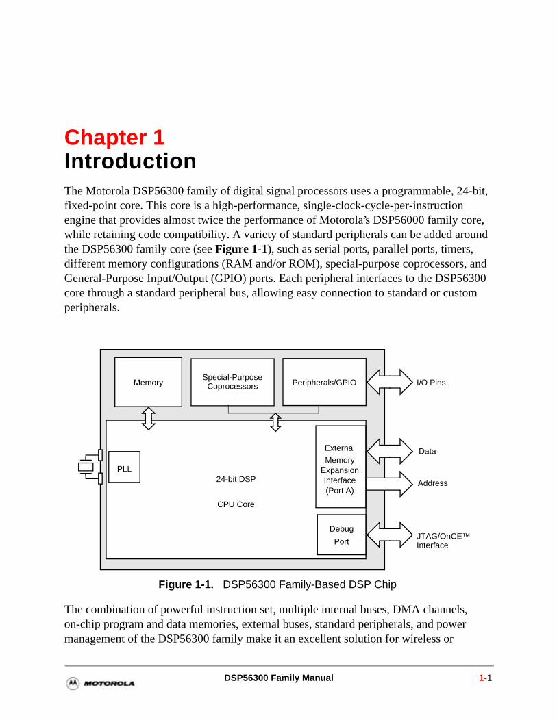
Chapter 1IntroductionThe Motorola DSP56300 family of digital signal processors uses a programmable, 24-bit, fixed-point core. This core is a high-performance, single-clock-cycle-per-instruction engine that provides almost twice the performance of Motorola’s DSP56000 family core, while retaining code compatibility. A variety of standard peripherals can be added around the DSP56300 family core (see Figure 1-1), such as serial ports, parallel ports, timers, different memory configurations (RAM and/or ROM), special-purpose coprocessors, and General-Purpose Input/Output (GPIO) ports. Each peripheral interfaces to the DSP56300 core through a standard peripheral bus, allowing easy connection to standard or custom peripherals.
The combination of powerful instruction set, multiple internal buses, DMA channels, on-chip program and data memories, external buses, standard peripherals, and power management of the DSP56300 family make it an excellent solution for wireless or
Figure 1-1. DSP56300 Family-Based DSP Chip
Address
Data
JTAG/OnCE™
Peripherals/GPIOMemory
24-bit DSP
CPU Core
Debug
Port
PLL
I/O Pins
External
Memory
Interface
Special-PurposeCoprocessors
ExpansionInterface(Port A)
DSP56300 Family Manual 1-1
Introduction
the
to
wireline DSP applications from individual subscriber to infrastructure, as well as multimedia and high-end audio applications, including videoconferencing.
1.1 Core Overview One Million Instructions Per Second (MIPS) per MHz of operating speed
Object code compatible with the DSP56000 core
Highly parallel instruction set
Data Arithmetic Logic Unit (Data ALU)
Address Generation Unit (AGU)
Program Control Unit (PCU)
On-chip instruction cache controller
External memory interface (Port A)
Phase Locked Loop (PLL)
Hardware debugging support (JTAG TAP, OnCETM module, and Address Trace Mode)
Six-channel Direct Memory Access (DMA) controller
Reduced power dissipation
— Very low power CMOS design
— Wait and Stop low-power standby modes
— Fully-static logic
1.1.1 Data Arithmetic Logic Unit (Data ALU)
The Data ALU performs all the arithmetic and logical operations on data operands inDSP56300 core. The components of the Data ALU are as follows:
Fully pipelined 24 × 24-bit parallel Multiplier-Accumulator (MAC) unit
Bit Field Unit, comprising a 56-bit parallel barrel shifter (fast shift and normalization; bit stream generation and parsing)
Conditional ALU instructions
24-bit or 16-bit arithmetic support under software control
Four 24-bit input general purpose registers: X1, X0, Y1, and Y0
Six Data ALU registers (A2, A1, A0, B2, B1, and B0) that are concatenated intwo general purpose 56-bit accumulators and accumulator shifters (A and B)
Two data bus shifter/limiter circuits
1-2 DSP56300 Family Manual
Core Overview
d and tored
rs used e, and four
s of to be Mn ddress
The Data ALU registers can be read or written over the X Data Bus (XDB) and the Y Data Bus (YDB) as 24- or 48-bit operands. The source operands for the Data ALU, which can be 24, 48, or 56 bits, always originate from the Data ALU registers. The results of all Data ALU operations are stored in an accumulator. All Data ALU operations are performed in two clock cycles in pipeline fashion so that a new instruction can be initiated in every clock, yielding an effective execution rate of one instruction per clock cycle.
The MAC unit comprises the main arithmetic processing unit of the DSP56300 core and performs all of the calculations on data operands. For arithmetic instructions, the unit accepts as many as three input operands and outputs one 56-bit result of the following form:
Extension:Most Significant Product:Least Significant Product (EXT:MSP:LSP)
The multiplier executes 24-bit × 24-bit, parallel fractional multiplies between two’s complement signed, unsigned, or mixed operands. The 48-bit product is right-justifieadded to the 56-bit contents of either the A or B accumulator. A 56-bit result can be sas a 24-bit operand by truncating or rounding the LSP into the MSP.
1.1.2 Address Generation Unit (AGU)
The Address Generation Unit (AGU) performs the effective address calculations for addressing data operands in memory and contains the integer arithmetic and registeto generate the addresses. The AGU operates in parallel with the other core resourcso minimizes address-generation overhead of instruction sequences. It implements types of address arithmetic:
Linear
Modulo
Multiple wrap-around modulo
Reverse-carry
These arithmetic types easily allow creation of data structures in memory for FIFOs (queues), delay lines, circular buffers, stacks, and bit-reversed FFT buffers. Data is manipulated by updating address registers (pointers) rather than moving large blockdata. The contents of the address modifier register, Mn, define the type of arithmeticperformed for addressing mode calculations. For modulo arithmetic, the contents ofalso specify the modulus. All address register indirect modes can be used with any amodifier. Each address register, Rn, has an associated modifier register, Mn. The following address modifier types are available.
Introduction 1-3
Introduction
d for
ne for
f nd a f coded
ull is a
operate arry
Linear addressing—Useful for general-purpose addressing
Modulo addressing—Useful for creating circular buffers for FIFOs
Multiple wrap-around modulo addressing—Useful for decimation, interpolationand waveform generation since the multiple wrap-around capability can be useargument reduction
Reverse-carry (bit-reverse) addressing—Useful for 2k-point FFT addressing
The AGU is divided into halves, each with its own Address Arithmetic Logic Unit (Address ALU), one to generate 24-bit addresses every cycle for the X space and othe Y space. Each Address ALU can update one address register from its respectiveaddress register file during one instruction cycle. Each Address ALU has four sets oregister triplets; each triplet is composed of an address register, an offset register, amodifier register. The contents of the associated modifier register specify the type oarithmetic to use in the address register update calculation. The modifier value is dein the Address ALU.
Each Address ALU contains a 24-bit full adder, which is an offset adder. A second fadder—which is a modulo adder—adds the summed result of the first full adder to amodulo value that is stored in its respective modifier register. A third full adder, whichreverse-carry adder, is also provided. The offset adder and the reverse-carry adder in parallel and share common inputs. The only difference between them is that the cpropagates in opposite directions. The modifier value determines which of the threesummed results of the full adders is output. For details on the AGU, see Chapter 4‚ Address
Generation Unit.
1.2 Program Control Unit (PCU)
The Program Control Unit (PCU) performs instruction fetch, instruction decoding, hardware DO loop control, and exception processing. The PCU implements a seven-stage pipeline and controls the different processing states of the DSP56300 core. The PCU consists of three hardware blocks:
Program Decode Controller (PDC): Decodes the 24-bit instruction loaded into the instruction latch and generates all necessary pipeline control signals
Program Address Generator (PAG): Contains the hardware for program address generation, system stack, and loop control
Program Interrupt Controller (PIC): Arbitrates among all interrupt requests (internal interrupts and the five external requests IRQA, IRQB, IRQC, IRQD, and NMI), and generates the appropriate interrupt vector address
1-4 DSP56300 Family Manual
On-chip Instruction Cache
PCU features include:
Position independent code (PIC) support
Addressing modes optimized for DSP applications (including immediate offsets)
On-chip instruction cache controller
On-chip memory-expandable hardware stack
Nested hardware DO loops
Fast auto-return interrupts
Program Address Trace mode support
1.3 On-chip Instruction Cache
The instruction cache functions as a buffer memory between external memory and the DSP core processor. When code executes, the code words at the locations requested by the instruction set are copied into the instruction cache for direct access by the core processor. If the same code is used frequently in a set of program instructions, storage of these instructions in the cache yields an increase in throughput, because external bus accesses are eliminated. In the DSP56300 instruction set are specific cache instructions that permit you to lock sectors of the cache and to flush the cache contents under software control. When enabled, the instruction cache has 1024 24-bit words (1 K words) of instruction cache memory, with the following features:
Software controlled Cache Enable (CE) bit in the Extended Mode Register (EMR) in the Status Register (SR)
Instruction cache size of 1024 24-bit words
Eight-way, fully associative instruction cache with sectored placement policy
1- to 4-word transfer granularity
Least recently used (LRU) sector replacement algorithm
Transparent operation (that is, no user management is required)
Individual sector locking/unlocking
Global cache flush controlled by software
Cache controller status observable via the JTAG/OnCE port
For more information, refer to Chapter 8‚ Instruction Cache.
Introduction 1-5
Introduction
ress s have s, the
o AA M
d
ow
e
1.4 Port A External Memory Interface
Port A is an external memory interface for memory expansion or memory-mapped I/O. Its programmable nature supports a low part-count connection to fast or slow SRAMs, DRAMs, I/O devices, and multiple bus master systems. The Port A data bus is 24 bits wide with a separate address bus that is 24 bits wide in some DSP56300 processors and less than 24 bits in others. External memory is divided into three possible 16 M × 24-bit spaces: X data, Y data, and program memory. Each or all spaces can be accessed to a given external memory under software control. See the memory map in Chapter 11‚
Operating Modes and Memory Spaces for memory space that is not accessible over Port A. An internal wait state generator can be programmed to statically insert up to 31 wait states for access to slower memory or I/O devices. A Transfer Acknowledge (TA) signal allows an external device to dynamically control the number of wait states inserted in a bus access operation. Bus arbitration signals allow an external device to use the bus while internal operations continue using internal memory. See the memory map in the device-specific user’s manual for memory space that is not accessible.
The Address Attribute (AA) lines operate as memory-mapped chip selects or as addlines to external devices, depending upon the mode selected. Some DSP56300 chipeighteen address lines. For these DSPs, if all four AA lines are used as address linetotal addressable external memory per space (X data, Y data, and program) is 4 M × 24-bit. If all four AA lines are used, the memory must always be selected because nlines are available for chip select. As a result, an external read or write outside the 4range could still go to the external memory (depending on the settings of the AA registers).
1.5 Phase Locked Loop (PLL) and Clock Generator
The clock generator in the DSP56300 core is composed of two main blocks:
Phase Locked Loop (PLL): Clock-input division, frequency multiplication, and skew elimination
Clock Generator (CLKGEN): Low-power division and clock pulse generation anchange of low-power Divide Factor (DF) without loss of lock
The PLL allows the processor to operate at a high internal clock frequency using a lfrequency clock input, a feature that offers two immediate benefits:
A lower frequency clock input reduces the overall electromagnetic interferencgenerated by a system.
The ability to oscillate at different frequencies reduces costs by eliminating theneed to add additional oscillators to a system.
1-6 DSP56300 Family Manual
Hardware Debugging Support
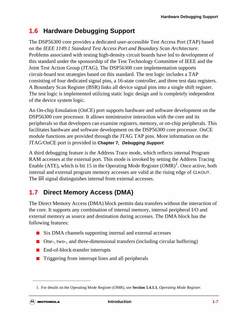
1.6 Hardware Debugging Support
The DSP56300 core provides a dedicated user-accessible Test Access Port (TAP) based on the IEEE 1149.1 Standard Test Access Port and Boundary Scan Architecture. Problems associated with testing high-density circuit boards have led to development of this standard under the sponsorship of the Test Technology Committee of IEEE and the Joint Test Action Group (JTAG). The DSP56300 core implementation supports circuit-board test strategies based on this standard. The test logic includes a TAP consisting of four dedicated signal pins, a 16-state controller, and three test data registers. A Boundary Scan Register (BSR) links all device signal pins into a single shift register. The test logic is implemented utilizing static logic design and is completely independent of the device system logic.
An On-chip Emulation (OnCE) port supports hardware and software development on the DSP56300 core processor. It allows nonintrusive interaction with the core and its peripherals so that developers can examine registers, memory, or on-chip peripherals. This facilitates hardware and software development on the DSP56300 core processor. OnCE module functions are provided through the JTAG TAP pins. More information on the JTAG/OnCE port is provided in Chapter 7‚ Debugging Support.
A third debugging feature is the Address Trace mode, which reflects internal Program RAM accesses at the external port. This mode is invoked by setting the Address Tracing Enable (ATE), which is bit 15 in the Operating Mode Register (OMR)1. Once active, both internal and external program memory accesses are valid at the rising edge of CLKOUT. The BR signal distinguishes internal from external accesses.
1.7 Direct Memory Access (DMA)
The Direct Memory Access (DMA) block permits data transfers without the interaction of the core. It supports any combination of internal memory, internal peripheral I/O and external memory as source and destination during accesses. The DMA block has the following features:
Six DMA channels supporting internal and external accesses
One-, two-, and three-dimensional transfers (including circular buffering)
End-of-block-transfer interrupts
Triggering from interrupt lines and all peripherals
1. For details on the Operating Mode Register (OMR), see Section 5.4.1.1, Operating Mode Register.
Introduction 1-7
Introduction
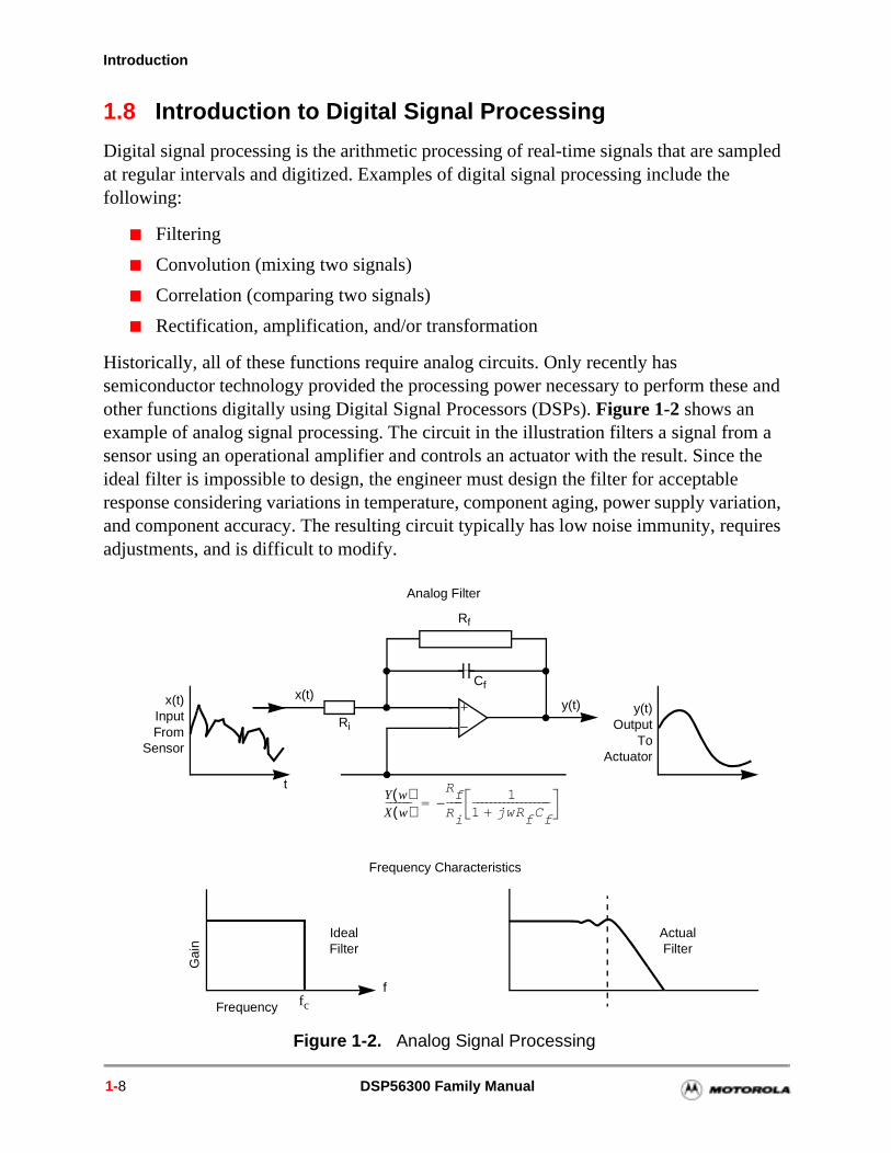
1.8 Introduction to Digital Signal Processing
Digital signal processing is the arithmetic processing of real-time signals that are sampled at regular intervals and digitized. Examples of digital signal processing include the following:
Filtering
Convolution (mixing two signals)
Correlation (comparing two signals)
Rectification, amplification, and/or transformation
Historically, all of these functions require analog circuits. Only recently has semiconductor technology provided the processing power necessary to perform these and other functions digitally using Digital Signal Processors (DSPs). Figure 1-2 shows an example of analog signal processing. The circuit in the illustration filters a signal from a sensor using an operational amplifier and controls an actuator with the result. Since the ideal filter is impossible to design, the engineer must design the filter for acceptable response considering variations in temperature, component aging, power supply variation, and component accuracy. The resulting circuit typically has low noise immunity, requires adjustments, and is difficult to modify.
Figure 1-2. Analog Signal Processing
x(t)InputFrom
Sensor
y(t)Output
ToActuator
t
x(t)
Ri
Rf
Cf
Analog Filter
Frequency Characteristics
IdealFilter
ffcFrequency
Gai
n
y(t)+–
ActualFilter
Y w( )X w( )------
RfRi----
11 jwRfCf+------------------–=
1-8 DSP56300 Family Manual
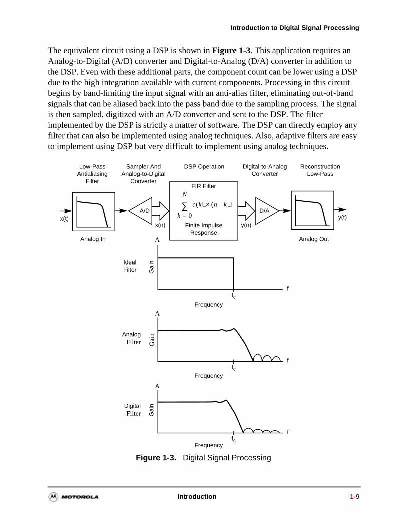
Introduction to Digital Signal Processing
The equivalent circuit using a DSP is shown in Figure 1-3. This application requires an Analog-to-Digital (A/D) converter and Digital-to-Analog (D/A) converter in addition to the DSP. Even with these additional parts, the component count can be lower using a DSP due to the high integration available with current components. Processing in this circuit begins by band-limiting the input signal with an anti-alias filter, eliminating out-of-band signals that can be aliased back into the pass band due to the sampling process. The signal is then sampled, digitized with an A/D converter and sent to the DSP. The filter implemented by the DSP is strictly a matter of software. The DSP can directly employ any filter that can also be implemented using analog techniques. Also, adaptive filters are easy to implement using DSP but very difficult to implement using analog techniques.
Figure 1-3. Digital Signal Processing
DSP Operation
FIR Filter
Finite ImpulseResponse
c k( ) n k–( )×
k 0=
N
∑A/D D/A
x(n) y(n)y(t)x(t)
Low-PassAntialiasing
Filter
Digital-to-AnalogConverter
ReconstructionLow-Pass
Analog Out
Sampler AndAnalog-to-Digital
Converter
Analog In A
IdealFilter
ffc
Frequency
Gai
n
AnalogFilter
ffc
Frequency
Gai
n
DigitalFilter
ffc
Frequency
Gai
n
A
A
Introduction 1-9
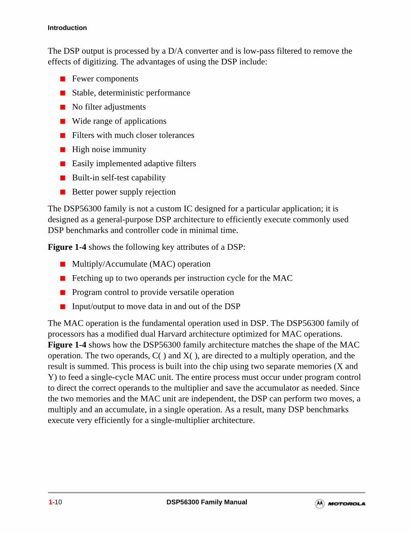
Introduction
The DSP output is processed by a D/A converter and is low-pass filtered to remove the effects of digitizing. The advantages of using the DSP include:
Fewer components
Stable, deterministic performance
No filter adjustments
Wide range of applications
Filters with much closer tolerances
High noise immunity
Easily implemented adaptive filters
Built-in self-test capability
Better power supply rejection
The DSP56300 family is not a custom IC designed for a particular application; it is designed as a general-purpose DSP architecture to efficiently execute commonly used DSP benchmarks and controller code in minimal time.
Figure 1-4 shows the following key attributes of a DSP:
Multiply/Accumulate (MAC) operation
Fetching up to two operands per instruction cycle for the MAC
Program control to provide versatile operation
Input/output to move data in and out of the DSP
The MAC operation is the fundamental operation used in DSP. The DSP56300 family of processors has a modified dual Harvard architecture optimized for MAC operations. Figure 1-4 shows how the DSP56300 family architecture matches the shape of the MAC operation. The two operands, C( ) and X( ), are directed to a multiply operation, and the result is summed. This process is built into the chip using two separate memories (X and Y) to feed a single-cycle MAC unit. The entire process must occur under program control to direct the correct operands to the multiplier and save the accumulator as needed. Since the two memories and the MAC unit are independent, the DSP can perform two moves, a multiply and an accumulate, in a single operation. As a result, many DSP benchmarks execute very efficiently for a single-multiplier architecture.
1-10 DSP56300 Family Manual
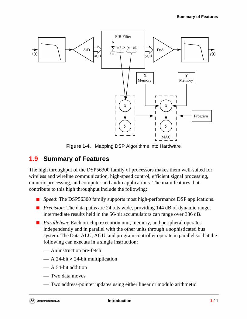
Summary of Features
1.9 Summary of Features
The high throughput of the DSP56300 family of processors makes them well-suited for wireless and wireline communication, high-speed control, efficient signal processing, numeric processing, and computer and audio applications. The main features that contribute to this high throughput include the following:
Speed: The DSP56300 family supports most high-performance DSP applications.
Precision: The data paths are 24 bits wide, providing 144 dB of dynamic range; intermediate results held in the 56-bit accumulators can range over 336 dB.
Parallelism: Each on-chip execution unit, memory, and peripheral operates independently and in parallel with the other units through a sophisticated bus system. The Data ALU, AGU, and program controller operate in parallel so that the following can execute in a single instruction:
— An instruction pre-fetch
— A 24-bit × 24-bit multiplication
— A 54-bit addition
— Two data moves
— Two address-pointer updates using either linear or modulo arithmetic
Figure 1-4. Mapping DSP Algorithms Into Hardware
FIR Filter
c k( ) n k–( )×
k 0=
N
∑A/Dx(t) x(n) y(n)
D/Ay(t)
Program
MAC
MemoryX
MemoryY
X X
∑ ∑
Introduction 1-11
Introduction
isters tus of
t ing the
mbly
s to
. The
er.
s that the s
this l, priate
Flexibility: While many other DSPs need external communications circuitry to interface with peripheral circuits (such as A/D converters, D/A converters, or host processors), the DSP56300 family provides on-chip serial and parallel interfaces that can support various configurations of memory and peripheral modules. The peripherals are interfaced to the DSP56300 family core through a peripheral interface bus that provides a common interface to many different peripherals.
Sophisticated Debugging: Motorola’s On-Chip Emulation (OnCE) technology allows simple, inexpensive, and speed independent access to the internal regfor debugging. With the OnCE module, you can determine easily the exact stathe registers and memory locations and what instructions were last executed.
Phase Locked Loop (PLL)-Based Clocking: The PLL allows the chip to use almosany available external system clock for full-speed operation, while also supplyan output clock synchronized to a synthesized internal core clock. It improvessynchronous timing of the external memory port, eliminating the timing skew common on other processors.
Invisible Pipeline: The seven-stage instruction pipeline is essentially invisible tothe programmer, allowing straightforward program development in either asselanguage or high-level languages such as C or C++.
Instruction Set: The instruction mnemonics are similar to those used for microcontroller units, making the transition from programming microprocessorprogramming the chip as easy as possible. New microcontroller instructions, addressing modes, and bit field instructions allow for significant decreases in program code size. The orthogonal syntax controls the parallel execution unitshardware DO loop instruction and the repeat (REP) instruction make writing straight-line code obsolete.
Low Power: Designed in CMOS, the DSP56300 family consumes very little powTwo additional low-power modes, Stop and Wait, further reduce power requirements. Wait is a low-power mode in which the DSP56300 family core ishut down, but the peripherals and interrupt controller continue to operate so an interrupt can bring the chip out of Wait mode. In Stop mode, even more of circuitry is shut down for the lowest power consumption. Several different wayexist to bring the chip out of Stop mode: hardware RESET, IRQA, and DE.
1.10 Manual Organization
This manual describes the DSP56300 family Central Processing Unit in detail. Use manual in conjunction with the appropriate DSP56300 family member user’s manuawhich describes the memory, operating modes, and peripheral modules. The approDSP56300 family technical data sheet describes timing, pinout, and packaging.
1-12 DSP56300 Family Manual
Manual Organization
This manual presents practical information to help the user accomplish the following:
Understand the operation and instruction set of the DSP56300 family
Write code for DSP algorithms
Write code for general control tasks
Write code for communication routines
Write code for data manipulation algorithms
Table 1-1 describes the contents of each chapter and each appendix.
Table 1-1. DSP Family Manual Chapters
Chapter/ Appendix
Title and Description
2 Core Architecture Overview—The DSP56300 family core architecture consists of an External Memory Interface (Port A), Data Arithmetic Logic Unit (Data ALU), Address Generation Unit (AGU), Program Control Unit (PCU), Direct Memory Access (DMA) controller, Phase Locked Loop (PLL) circuit, and a JTAG/On-Chip Emulation (OnCE) port. Chapter 2 describes each subsystem and the buses interconnecting the major components in the DSP56300 family central processing module. Chapter 2 also describes five of the six processing states (Normal, Exception, Reset, Wait, and Stop). The sixth processing state (Debug) is covered more completely in Chapter 7‚ Debugging Support.
3 Data Arithmetic Logic Unit —Data ALU architecture, its programming model, an introduction to fractional and integer arithmetic, and a discussion of other topics such as unsigned and multi-precision arithmetic on the DSP56300 family.
4 Address Generation Unit—AGU architecture, its programming model, addressing modes, and address modifiers.
5 Program Control Unit—Program controller architecture, its programming model, and hardware looping. Note, however, that the different processing states of the DSP56300 family core, including interrupt processing, are described in Chapter 2‚ Core Architecture Overview.
6 PLL and Clock Generator —Details the PLL, its programming model, and its general operation.
7 Debugging Support—Combined JTAG/OnCE port and its functions. These two are integrally related, sharing the same pins for I/O.
8 Instruction Cache—Operation of the instruction cache and memory space.
9 External Memory Interface (Port A)—The External Memory Interface, its programming model, and guidelines for interfacing SRAM and DRAM.
10 DMA Controller—The six-channel Direct Memory Access (DMA) controller, its programming model, and interactions with the core and peripherals.
11 Operating Modes and Memory Spaces—Operating modes and memory spaces in the DSP56300 family.
12 Guide to the Instruction Set — The DSP56300 family instruction format as well as partial encodings for use in instruction encoding
Introduction 1-13
Introduction
found
s if fer to the
red,”
Vrt” s
sed in
The latest electronic version of this document as well as other DSP documentation (including user’s manuals, product briefs, technical data sheets, and errata) can be on the Motorola DSP World Wide Web site: http://www.motorola.com/SPS/DSP
1.11 Manual Conventions
This manual uses the following conventions:
Bits within registers are always listed from most significant bit (MSB) to least significant bit (LSB).
Bits within a register are indicated by AA[n – m], when more than one bit is involved in a description. For purposes of description, the bits are presented athey are contiguous within a register. However, this is not always the case. Rethe programming model diagrams in the device-specific user’s manual to seeexact location of bits within a register.
When a bit is described as “set,” its value is 1. When a bit is described as “cleaits value is 0.
The word “assert” means that a high true (active high) signal is pulled high to CC or that a low true (active low) signal is pulled low to ground. The word “deassemeans that a high true signal is pulled low to ground or that a low true signal ipulled high to VCC. See Table 1-2.
Signals in a range are indicated by the first and last signals in the range enclosquare brackets, for example A[0 – 23].
13 Instruction Set — Each DSP56300 family instruction, its use, and its effect on the processor.
A Instruction Timing and Restrictions— Various aspects of execution timing analysis for each instruction, sequences that may cause timing delays or stalls, and programming restrictions.
B Benchmark Programs—DSP56300 family benchmark example programs and results.
C From CDR Process to HiP Process — General differences between DSP56300 family derivatives that use Motorola’s Communication Design Rules (CDR) process technology and derivatives that use Motorola’s High-Performance (HiP) process technology; software and hardware design implications.
Table 1-1. DSP Family Manual Chapters (Continued)
Chapter/ Appendix
Title and Description
1-14 DSP56300 Family Manual
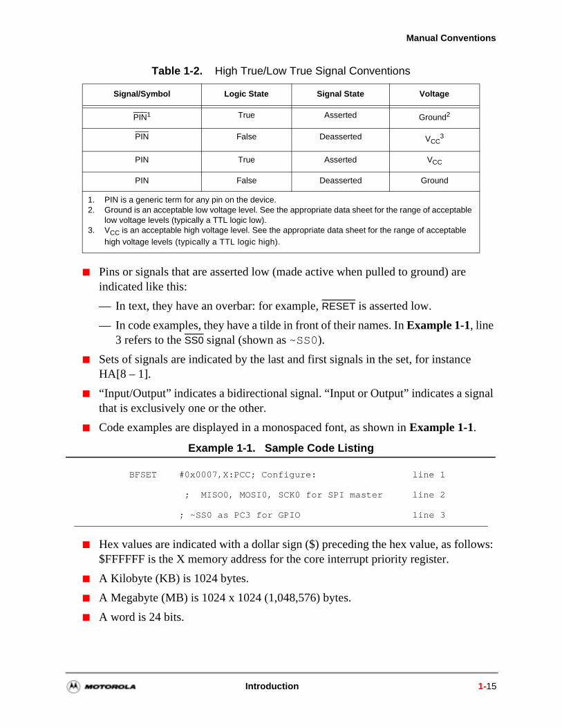
Manual Conventions
e
nal
ows:
Pins or signals that are asserted low (made active when pulled to ground) are indicated like this:
— In text, they have an overbar: for example, RESET is asserted low.
— In code examples, they have a tilde in front of their names. In Example 1-1, line 3 refers to the SS0 signal (shown as ~SS0).
Sets of signals are indicated by the last and first signals in the set, for instancHA[8 – 1].
“Input/Output” indicates a bidirectional signal. “Input or Output” indicates a sigthat is exclusively one or the other.
Code examples are displayed in a monospaced font, as shown in Example 1-1.
Hex values are indicated with a dollar sign ($) preceding the hex value, as foll$FFFFFF is the X memory address for the core interrupt priority register.
A Kilobyte (KB) is 1024 bytes.
A Megabyte (MB) is 1024 x 1024 (1,048,576) bytes.
A word is 24 bits.
Table 1-2. High True/Low True Signal Conventions
Signal/Symbol Logic State Signal State Voltage
PIN1 True Asserted Ground2
PIN False Deasserted VCC3
PIN True Asserted VCC
PIN False Deasserted Ground
1. PIN is a generic term for any pin on the device.2. Ground is an acceptable low voltage level. See the appropriate data sheet for the range of acceptable
low voltage levels (typically a TTL logic low).3. VCC is an acceptable high voltage level. See the appropriate data sheet for the range of acceptable
high voltage levels (typically a TTL logic high).
Example 1-1. Sample Code Listing
BFSET #0x0007,X:PCC; Configure: line 1
; MISO0, MOSI0, SCK0 for SPI master line 2
; ~SS0 as PC3 for GPIO line 3
Introduction 1-15

Introduction
The word “reset” appears in four different contexts in this manual:
— the reset signal, written as RESET
— the reset instruction, written as RESET
— the reset operating state, written as Reset
— the reset function, written as reset
1-16 DSP56300 Family Manual
Chapter 2Core Architecture OverviewThis chapter describes the DSP56300 family core, a powerful DSP engine that can execute an instruction on every clock cycle, yielding almost twice the performance of the Motorola DSP56000 core while retaining object code compatibility.
The parts of the DSP56300 core are described in the following chapters:
Chapter 3, Data Arithmetic Logic Unit (Data ALU)
Chapter 4, Address Generation Unit (AGU)
Chapter 5, Program Control Unit (PCU)
Chapter 6, PLL and Clock Generator
Chapter 7, Debugging Support (JTAG TAP and OnCE Module)
Chapter 8, Instruction Cache
Chapter 9, External Memory Interface (Port A)
Chapter 10, DMA Controller
To minimize the total system cost for customer applications, the DSP56300 core external memory interface, Port A, is powerful and versatile, providing a glueless interface to DRAMs (in some DSPs), SRAMs, and other memories via an on-chip DRAM controller (in some DSPs) as well as chip select logic. To assist with data movement over Port A and internally, the concurrent six-channel DMA augments the data throughput that characterizes DSP applications.
The core is designed for low power consumption in Normal and Wait and Stop modes. In Normal mode, only the blocks demanded for processing are active. Wait and Stop modes take the power savings a step further by closing down large portions of the core during periods of system inactivity. The integrated on-chip peripherals and memory (including instruction cache) also reduce power consumption by reducing the external bus accesses. As for the core execution units, only the memory modules being accessed consume power, so on-chip memory expansion does not increase power significantly. Limiting the external bus accesses saves on system power. Finally, the Phase Locked Loop (PLL) can scale power consumption down with lower clock frequencies under user software control.
DSP56300 Family Manual 2-1
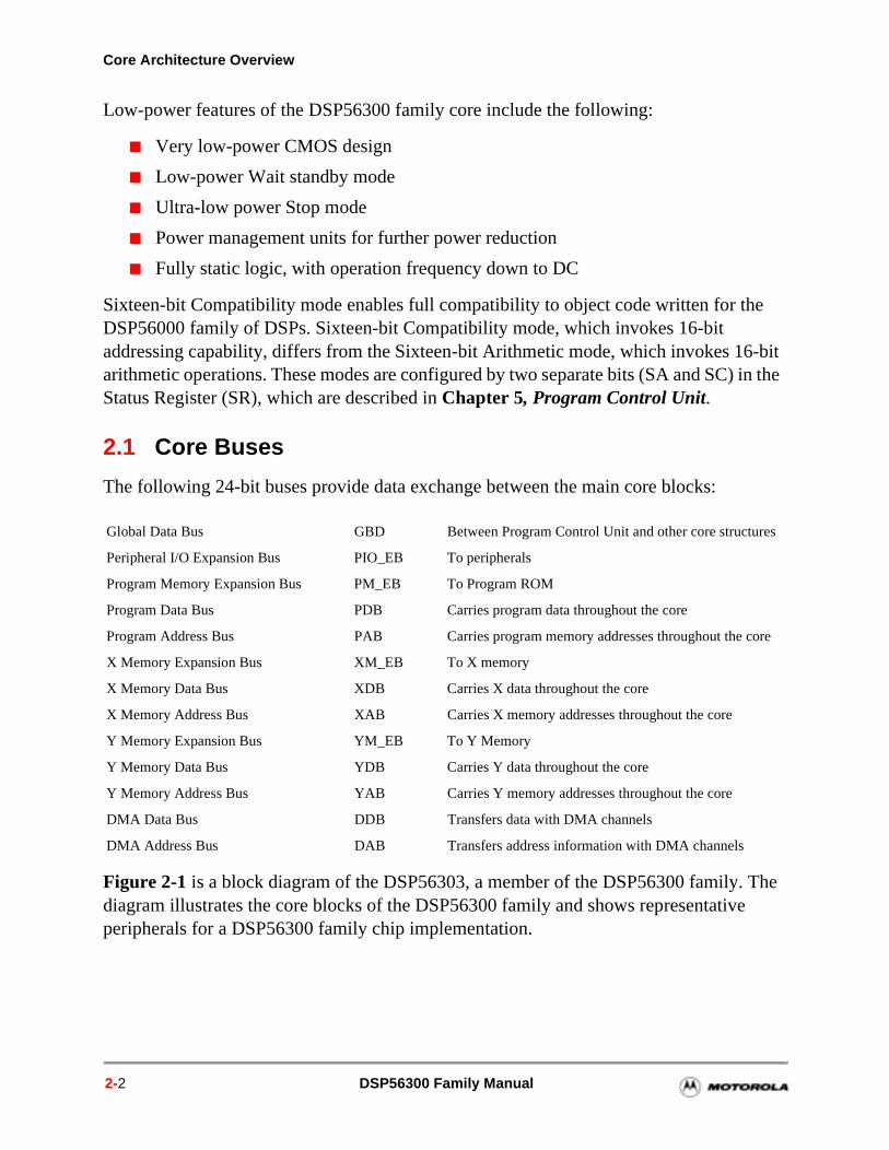
Core Architecture Overview
Low-power features of the DSP56300 family core include the following:
Very low-power CMOS design
Low-power Wait standby mode
Ultra-low power Stop mode
Power management units for further power reduction
Fully static logic, with operation frequency down to DC
Sixteen-bit Compatibility mode enables full compatibility to object code written for the DSP56000 family of DSPs. Sixteen-bit Compatibility mode, which invokes 16-bit addressing capability, differs from the Sixteen-bit Arithmetic mode, which invokes 16-bit arithmetic operations. These modes are configured by two separate bits (SA and SC) in the Status Register (SR), which are described in Chapter 5, Program Control Unit.
2.1 Core Buses
The following 24-bit buses provide data exchange between the main core blocks:
Figure 2-1 is a block diagram of the DSP56303, a member of the DSP56300 family. The diagram illustrates the core blocks of the DSP56300 family and shows representative peripherals for a DSP56300 family chip implementation.
Global Data Bus GBD Between Program Control Unit and other core structures
Peripheral I/O Expansion Bus PIO_EB To peripherals
Program Memory Expansion Bus PM_EB To Program ROM
Program Data Bus PDB Carries program data throughout the core
Program Address Bus PAB Carries program memory addresses throughout the core
X Memory Expansion Bus XM_EB To X memory
X Memory Data Bus XDB Carries X data throughout the core
X Memory Address Bus XAB Carries X memory addresses throughout the core
Y Memory Expansion Bus YM_EB To Y Memory
Y Memory Data Bus YDB Carries Y data throughout the core
Y Memory Address Bus YAB Carries Y memory addresses throughout the core
DMA Data Bus DDB Transfers data with DMA channels
DMA Address Bus DAB Transfers address information with DMA channels
2-2 DSP56300 Family Manual
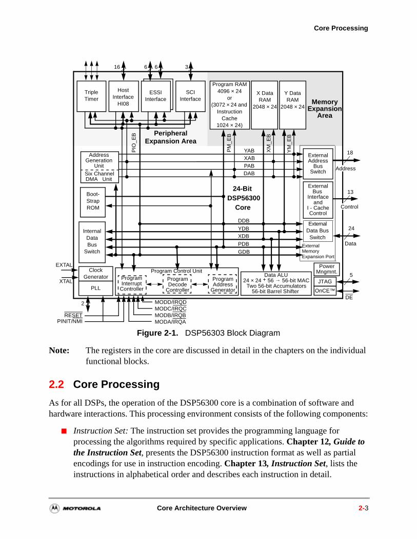
Core Processing
Note: The registers in the core are discussed in detail in the chapters on the individual functional blocks.
2.2 Core Processing
As for all DSPs, the operation of the DSP56300 core is a combination of software and hardware interactions. This processing environment consists of the following components:
Instruction Set: The instruction set provides the programming language for processing the algorithms required by specific applications. Chapter 12, Guide to the Instruction Set, presents the DSP56300 instruction format as well as partial encodings for use in instruction encoding. Chapter 13, Instruction Set, lists the instructions in alphabetical order and describes each instruction in detail.
Figure 2-1. DSP56303 Block Diagram
PLL OnCE™
ClockGenerator
Internal DataBus
Switch
YABXABPAB
YDBXDB
PDB
GDB
MODC/IRQCMODB/IRQB
ExternalData Bus
Switch
13
MODA/IRQA
DSP56300
616
24-Bit
24
18
DDB
DAB
Peripheral
Core
YM
_EB
XM
_EB
PM
_EB
PIO
_EB
Expansion Area
6
SCIInterface
JTAG5
3
RESET
MODD/IRQD
PINIT/NMI
2
Boot-StrapROM
EXTAL
XTAL
Address
Control
Data
TripleTimer
HostInterface
HI08
ESSIInterface
AddressGeneration
Unit
Six ChannelDMA Unit
ProgramInterrupt
Controller
ProgramDecode
Controller
ProgramAddress
Generator
Data ALU24 × 24 + 56 → 56-bit MAC
Two 56-bit Accumulators56-bit Barrel Shifter
PowerMngmnt.
ExternalBus
Interface and
I - CacheControl
ExternalAddress
BusSwitch
MemoryExpansion
Area
DE
Program RAM4096 × 24
or(3072 × 24 and
Instruction Cache
1024 × 24)
X DataRAM
2048 × 24
Y DataRAM
2048 × 24
Program Control Unit
External Memory Expansion Port
Core Architecture Overview 2-3
Core Architecture Overview
ssor
lts rating
pical
als g
the ither
ly curs
a
not LL is
the . In
Core Modules: These circuits transfer and modify data. They are generally configured through internal registers and activated or disabled by a combination of hardware signals (interrupts, request signals, and so on) and software. Chapters 3-10 of this document describe the structure and function of the various core modules.
Processing States: Core processing states modify the operation of the core processor and the core modules that operate independently and in parallel to the core. These states include:
— Normal: The typical operating mode in which code loads into the core proceand executes.
— Exception: An event interrupts the normal execution flow. The processor hanormal processing and, depending on the event, may store the current opeenvironment, load a special handler program to respond to the exception, execute the handler program, and then return to normal execution flow. Tyexception causes can be software processing events or hardware service requests, such as peripheral or external device interrupts.
— Reset: All execution halts and the processor and its registers in all peripherare restored to a predetermined value that allows reloading of the executincode and reinitiation of the execution flow. Typically, if an operation has caused an unrecoverable error (that is, the handler cannot compensate forexception event that halted normal processing), invoking the Reset mode, eby software or by asserting the physical RESET signal, restores operational functioning.
— Wait: Typically invoked by the WAIT instruction; the application requires onminimal processing. To save power, most operations stop until an event octhat requires the processing to restart. Clock signals remain functional, so quick restart is possible.
— Stop: Typically invoked by using the STOP instruction; the application does require immediate processing and a slow restart is acceptable (only if the Pdisabled). All clock functions and operations halt, except for the ability to respond to an initiating event (that is, RESET, DE, or IRQA).
— Debug: Application developers can operate the system under the control ofJTAG Test Access Port and Boundary Scan function or the OnCE modulethis mode, an application can run a single instruction at a time, or sets of instructions at a time, until some defined event occurs, typically called a breakpoint.
2-4 DSP56300 Family Manual
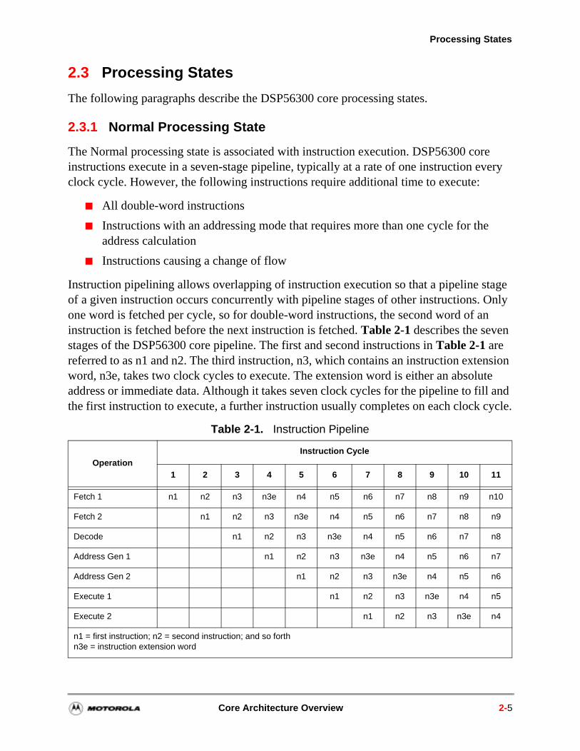
Processing States
2.3 Processing States
The following paragraphs describe the DSP56300 core processing states.
2.3.1 Normal Processing State
The Normal processing state is associated with instruction execution. DSP56300 core instructions execute in a seven-stage pipeline, typically at a rate of one instruction every clock cycle. However, the following instructions require additional time to execute:
All double-word instructions
Instructions with an addressing mode that requires more than one cycle for the address calculation
Instructions causing a change of flow
Instruction pipelining allows overlapping of instruction execution so that a pipeline stage of a given instruction occurs concurrently with pipeline stages of other instructions. Only one word is fetched per cycle, so for double-word instructions, the second word of an instruction is fetched before the next instruction is fetched. Table 2-1 describes the seven stages of the DSP56300 core pipeline. The first and second instructions in Table 2-1 are referred to as n1 and n2. The third instruction, n3, which contains an instruction extension word, n3e, takes two clock cycles to execute. The extension word is either an absolute address or immediate data. Although it takes seven clock cycles for the pipeline to fill and the first instruction to execute, a further instruction usually completes on each clock cycle.
Table 2-1. Instruction Pipeline
OperationInstruction Cycle
1 2 3 4 5 6 7 8 9 10 11
Fetch 1 n1 n2 n3 n3e n4 n5 n6 n7 n8 n9 n10
Fetch 2 n1 n2 n3 n3e n4 n5 n6 n7 n8 n9
Decode n1 n2 n3 n3e n4 n5 n6 n7 n8
Address Gen 1 n1 n2 n3 n3e n4 n5 n6 n7
Address Gen 2 n1 n2 n3 n3e n4 n5 n6
Execute 1 n1 n2 n3 n3e n4 n5
Execute 2 n1 n2 n3 n3e n4
n1 = first instruction; n2 = second instruction; and so forthn3e = instruction extension word
Core Architecture Overview 2-5
Core Architecture Overview
Each instruction requires a minimum of seven clock cycles to fetch, decode, and execute. This results in a delay of seven clock cycles from power-up to fill the pipeline. A new instruction may begin immediately following the previous instruction. Two-word instructions require a minimum of eight clock cycles to execute (seven cycles for the first instruction word to move through the pipe and execute and one more cycle for the second word to execute). For a complete description of the execution timing of the various instructions, see Appendix A, Instruction Timing and Restrictions.
2.3.2 Exception Processing State (Interrupt Processing)
The Exception Processing state is associated with interrupts that are generated by conditions inside the DSP or by external sources. There are many sources for interrupts to the DSP56300 core, some generating more than one interrupt. An interrupt vector scheme with 128 vectors of defined priority provides fast interrupt service. Interrupt processing in the DSP56300 core proceeds as follows:
1. A hardware interrupt is synchronized with the DSP56300 core clock, and the interrupt pending flag for that particular hardware interrupt is set. An interrupt source can have only one interrupt pending at any given time.
2. All pending interrupts (external and internal) are arbitrated to select the interrupt to be processed. The arbiter automatically ignores any interrupts with an Interrupt Priority Level (IPL) lower than the interrupt mask level in the SR and selects the remaining interrupt with the highest IPL.
3. The interrupt controller freezes the Program Counter (PC) and fetches two instructions at the two interrupt vector addresses associated with the selected interrupt.
4. The interrupt controller inserts the two instructions into the instruction stream and releases the PC, which is used for the next instruction fetch. The next interrupt arbitration then begins.
When a fast interrupt executes, the state of the machine is not saved on the stack if neither of the two instructions is a Jump To Subroutine (JSR) instruction (for example, a JSCLR). A long interrupt executes if one of the interrupt instructions fetched is a JSR instruction. The PC is immediately released, the SR and the PC are saved in the stack, and the jump instruction controls from where the next instruction is fetched.
Note: Any Jump to Subroutine (JSR) instruction makes the interrupt long (for example, JScc, BSSET, and so on.).
One of the main uses of interrupts is to transfer data between DSP memory or registers and a peripheral device. When such an interrupt occurs, a limited context switch with
2-6 DSP56300 Family Manual
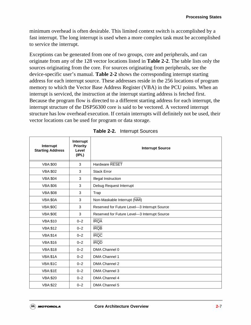
Processing States
ogram an
t, the their
minimum overhead is often desirable. This limited context switch is accomplished by a fast interrupt. The long interrupt is used when a more complex task must be accomplished to service the interrupt.
Exceptions can be generated from one of two groups, core and peripherals, and can originate from any of the 128 vector locations listed in Table 2-2. The table lists only the sources originating from the core. For sources originating from peripherals, see the device-specific user’s manual. Table 2-2 shows the corresponding interrupt starting address for each interrupt source. These addresses reside in the 256 locations of prmemory to which the Vector Base Address Register (VBA) in the PCU points. Wheninterrupt is serviced, the instruction at the interrupt starting address is fetched first. Because the program flow is directed to a different starting address for each interrupinterrupt structure of the DSP56300 core is said to be vectored. A vectored interruptstructure has low overhead execution. If certain interrupts will definitely not be used,vector locations can be used for program or data storage.
Table 2-2. Interrupt Sources
InterruptStarting Address
Interrupt Priority Level (IPL)
Interrupt Source
VBA:$00 3 Hardware RESET
VBA:$02 3 Stack Error
VBA:$04 3 Illegal Instruction
VBA:$06 3 Debug Request Interrupt
VBA:$08 3 Trap
VBA:$0A 3 Non-Maskable Interrupt (NMI)
VBA:$0C 3 Reserved for Future Level—3 Interrupt Source
VBA:$0E 3 Reserved for Future Level—3 Interrupt Source
VBA:$10 0–2 IRQA
VBA:$12 0–2 IRQB
VBA:$14 0–2 IRQC
VBA:$16 0–2 IRQD
VBA:$18 0–2 DMA Channel 0
VBA:$1A 0–2 DMA Channel 1
VBA:$1C 0–2 DMA Channel 2
VBA:$1E 0–2 DMA Channel 3
VBA:$20 0–2 DMA Channel 4
VBA:$22 0–2 DMA Channel 5
Core Architecture Overview 2-7
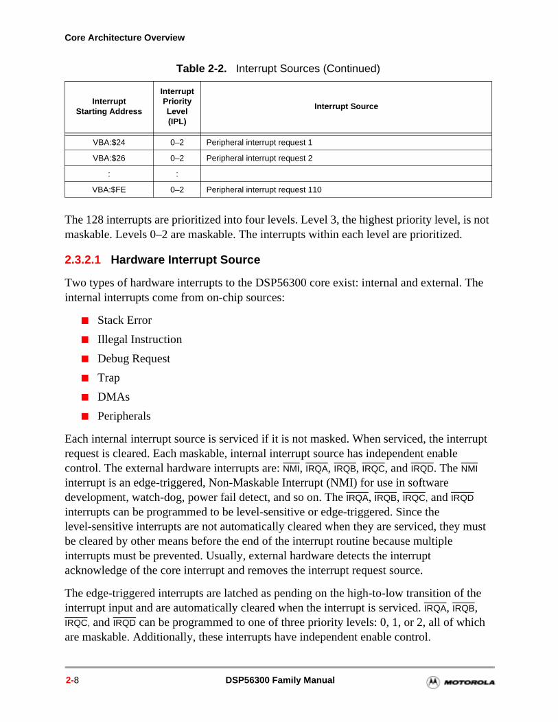
Core Architecture Overview
The
rrupt
must
the
ich
The 128 interrupts are prioritized into four levels. Level 3, the highest priority level, is not maskable. Levels 0–2 are maskable. The interrupts within each level are prioritized.
2.3.2.1 Hardware Interrupt Source
Two types of hardware interrupts to the DSP56300 core exist: internal and external.internal interrupts come from on-chip sources:
Stack Error
Illegal Instruction
Debug Request
Trap
DMAs
Peripherals
Each internal interrupt source is serviced if it is not masked. When serviced, the interequest is cleared. Each maskable, internal interrupt source has independent enablecontrol. The external hardware interrupts are: NMI, IRQA, IRQB, IRQC, and IRQD. The NMI interrupt is an edge-triggered, Non-Maskable Interrupt (NMI) for use in software development, watch-dog, power fail detect, and so on. The IRQA, IRQB, IRQC, and IRQD interrupts can be programmed to be level-sensitive or edge-triggered. Since the level-sensitive interrupts are not automatically cleared when they are serviced, theybe cleared by other means before the end of the interrupt routine because multiple interrupts must be prevented. Usually, external hardware detects the interrupt acknowledge of the core interrupt and removes the interrupt request source.
The edge-triggered interrupts are latched as pending on the high-to-low transition ofinterrupt input and are automatically cleared when the interrupt is serviced. IRQA, IRQB, IRQC, and IRQD can be programmed to one of three priority levels: 0, 1, or 2, all of whare maskable. Additionally, these interrupts have independent enable control.
VBA:$24 0–2 Peripheral interrupt request 1
VBA:$26 0–2 Peripheral interrupt request 2
: :
VBA:$FE 0–2 Peripheral interrupt request 110
Table 2-2. Interrupt Sources (Continued)
InterruptStarting Address
Interrupt Priority Level (IPL)
Interrupt Source
2-8 DSP56300 Family Manual
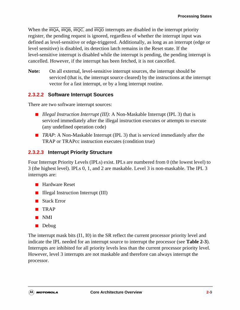
Processing States
When the IRQA, IRQB, IRQC, and IRQD interrupts are disabled in the interrupt priority register, the pending request is ignored, regardless of whether the interrupt input was defined as level-sensitive or edge-triggered. Additionally, as long as an interrupt (edge or level sensitive) is disabled, its detection latch remains in the Reset state. If the level-sensitive interrupt is disabled while the interrupt is pending, the pending interrupt is cancelled. However, if the interrupt has been fetched, it is not cancelled.
Note: On all external, level-sensitive interrupt sources, the interrupt should be serviced (that is, the interrupt source cleared) by the instructions at the interrupt vector for a fast interrupt, or by a long interrupt routine.
2.3.2.2 Software Interrupt Sources
There are two software interrupt sources:
Illegal Instruction Interrupt (III): A Non-Maskable Interrupt (IPL 3) that is serviced immediately after the illegal instruction executes or attempts to execute (any undefined operation code)
TRAP: A Non-Maskable Interrupt (IPL 3) that is serviced immediately after the TRAP or TRAPcc instruction executes (condition true)
2.3.2.3 Interrupt Priority Structure
Four Interrupt Priority Levels (IPLs) exist. IPLs are numbered from 0 (the lowest level) to 3 (the highest level). IPLs 0, 1, and 2 are maskable. Level 3 is non-maskable. The IPL 3 interrupts are:
Hardware Reset
Illegal Instruction Interrupt (III)
Stack Error
TRAP
NMI
Debug
The interrupt mask bits (I1, I0) in the SR reflect the current processor priority level and indicate the IPL needed for an interrupt source to interrupt the processor (see Table 2-3). Interrupts are inhibited for all priority levels less than the current processor priority level. However, level 3 interrupts are not maskable and therefore can always interrupt the processor.
Core Architecture Overview 2-9
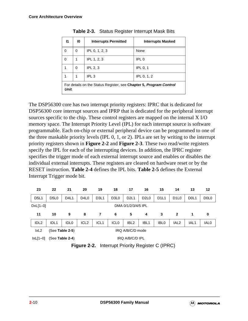
Core Architecture Overview
The DSP56300 core has two interrupt priority registers: IPRC that is dedicated for DSP56300 core interrupt sources and IPRP that is dedicated for the peripheral interrupt sources specific to the chip. These control registers are mapped on the internal X I/O memory space. The Interrupt Priority Level (IPL) for each interrupt source is software programmable. Each on-chip or external peripheral device can be programmed to one of the three maskable priority levels (IPL 0, 1, or 2). IPLs are set by writing to the interrupt priority registers shown in Figure 2-2 and Figure 2-3. These two read/write registers specify the IPL for each of the interrupting devices. In addition, the IPRC register specifies the trigger mode of each external interrupt source and enables or disables the individual external interrupts. These registers are cleared on hardware reset or by the RESET instruction. Table 2-4 defines the IPL bits. Table 2-5 defines the External Interrupt Trigger mode bit.
Table 2-3. Status Register Interrupt Mask Bits
I1 I0 Interrupts Permitted Interrupts Masked
0 0 IPL 0, 1, 2, 3 None
0 1 IPL 1, 2, 3 IPL 0
1 0 IPL 2, 3 IPL 0, 1
1 1 IPL 3 IPL 0, 1, 2
For details on the Status Register, see Chapter 5, Program Control Unit.
23 22 21 20 19 18 17 16 15 14 13 12
D5L1 D5L0 D4L1 D4L0 D3L1 D3L0 D2L1 D2L0 D1L1 D1L0 D0L1 D0L0
DxL[1–0] DMA 0/1/2/3/4/5 IPL
11 10 9 8 7 6 5 4 3 2 1 0
IDL2 IDL1 IDL0 ICL2 ICL1 ICL0 IBL2 IBL1 IBL0 IAL2 IAL1 IAL0
IxL2 (See Table 2-5) IRQ A/B/C/D mode
IxL[1–0] (See Table 2-4) IRQ A/B/C/D IPL
Figure 2-2. Interrupt Priority Register C (IPRC)
2-10 DSP56300 Family Manual
Processing States
If more than one exception is pending when an instruction executes, the interrupt with the highest priority level is serviced first. When multiple interrupt requests with the same IPL are pending, a second fixed-priority structure within that IPL determines which interrupt is serviced. Table 2-6 shows the interrupt priority for all interrupts.
Table 2-4. Interrupt Priority Level Bits
IxL1 IxL0 Enabled IPL
0 0 No —
0 1 Yes 0
1 0 Yes 1
1 1 Yes 2
Table 2-5. External Interrupt Trigger Mode Bit
IxL2 Trigger Mode
0 Level
1 Negative Edge
23 22 21 20 19 18 17 16 15 14 13 12
PerCL1 PerCL0 PerBL1 PerBL0 PerAL1 PerAL0 Per9L1 Per9L0 Per8L1 Per8L0 Per7L1 Per7L0
11 10 9 8 7 6 5 4 3 2 1 0
Per6L1 Per6L0 Per5L1 Per5L0 Per4L1 Per4L0 Per3L1 Per3L0 Per2L1 Per2L0 Per1L1 Per1L0
Figure 2-3. Interrupt Priority Register P (IPRP)
Core Architecture Overview 2-11
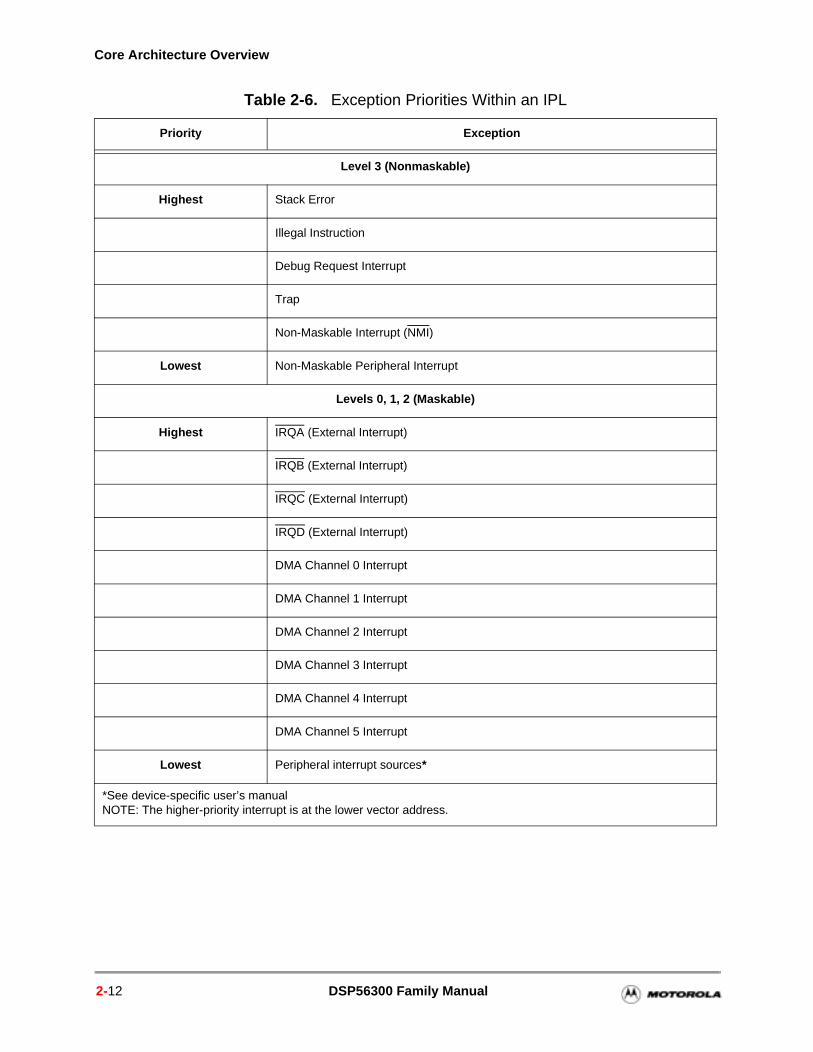
Core Architecture Overview
Table 2-6. Exception Priorities Within an IPL
Priority Exception
Level 3 (Nonmaskable)
Highest Stack Error
Illegal Instruction
Debug Request Interrupt
Trap
Non-Maskable Interrupt (NMI)
Lowest Non-Maskable Peripheral Interrupt
Levels 0, 1, 2 (Maskable)
Highest IRQA (External Interrupt)
IRQB (External Interrupt)
IRQC (External Interrupt)
IRQD (External Interrupt)
DMA Channel 0 Interrupt
DMA Channel 1 Interrupt
DMA Channel 2 Interrupt
DMA Channel 3 Interrupt
DMA Channel 4 Interrupt
DMA Channel 5 Interrupt
Lowest Peripheral interrupt sources*
*See device-specific user’s manualNOTE: The higher-priority interrupt is at the lower vector address.
2-12 DSP56300 Family Manual
Processing States
irst
of the
s,
that
e
es
2.3.2.4 Instructions Preceding the Interrupt Instruction Fetch
The following conditions apply to instructions preceding an interrupt instruction fetch:
Every instruction requiring more than one cycle to execute is aborted when it is fetched in the cycle preceding the fetch of the first interrupt instruction word.
Aborted instructions are fetched again when program control returns from the interrupt routine. The PC is adjusted appropriately before the end of the decode cycle of the aborted instruction.
If the first interrupt word fetch occurs in the cycle following the fetch of a one-word-one-cycle instruction, that instruction completes normally before the start of the interrupt routine.
During an interrupt instruction fetch, two instruction words are fetched — the ffrom the interrupt starting address and the second from the next address.
2.3.2.5 Interrupt Types
Two types of interrupt routines can be used: fast and long. The fast routine consiststwo automatically inserted interrupt instruction words. These words can be any unrestricted, single two-word instruction or any two unrestricted one-word instructionexcept RTI or RTS. Fast interrupt routines are not interruptible.
Note: Status is not preserved during a fast interrupt routine; therefore, instructionsmodify status should not be used at the interrupt starting address or next address.
If one of the instructions in the fast routine is a JSR, then a long interrupt routine is formed. The following actions occur during execution of the JSR instruction when it occurs in the interrupt starting address or in the next address:
1. The PC (containing the return address) and the SR are stacked.
2. The Loop Flag is cleared.
3. The Scaling mode bits (S[1–0]) in the Status Register (SR) are cleared.
4. The Sixteen-bit Arithmetic (SA) mode bit is cleared.
5. The IPL is raised to disallow further interrupts of the same or lower levels. SeTable 2-6.
Only the long interrupt routine should be terminated by an RTI. Long interrupt routinare interruptible by higher-priority interrupts.
Note: Do not use RTI for fast interrupts.
Core Architecture Overview 2-13
Core Architecture Overview
rupt rupts
upt
pt is
s to next dress fter ction
and tion
any n
s ain ne.
ded
2.3.2.6 Interrupt Arbitration
External interrupts are internally synchronized with the processor clock before their interrupt-pending flags are set. Each external interrupt and internal interrupt has its own flag. After each instruction executes, all interrupts are arbitrated (that is, all hardware interrupts that have been latched into their respective interrupt-pending flags and all internal interrupts). During arbitration, each interrupt’s IPL is compared with the intermask in the SR, and the interrupt is either allowed or disallowed. The remaining interare prioritized according to the priority shown in Table 2-6, and the highest priority interrupt is chosen. The interrupt vector is then calculated so that the program interrcontroller can fetch the first interrupt instruction. The interrupt-pending flag for the chosen interrupt is not cleared until the second interrupt vector of the chosen interrufetched. A new interrupt from the same source is not accepted for the next interrupt arbitration until the interrupt-pending flag is cleared.
2.3.2.7 Interrupt Instruction Fetch
The interrupt controller generates an interrupt instruction fetch address, which pointthe first instruction word of a two-word interrupt routine. This address is used for theinstruction fetch, instead of the contents of the PC, and again for the subsequent adafter that. While the interrupt instructions are being fetched, the PC is not updated. Athe two interrupt words have been fetched, the PC is used for any subsequent instrufetches.
2.3.2.8 Interrupt Instruction Execution
Interrupt instruction execution is considered “fast” if neither of the instructions of theinterrupt service routine cause a change of flow. A JSR within a fast interrupt routineforms a long interrupt, which is terminated with an RTI instruction to restore the PC SR from the stack and return to normal program execution. Reset is a special excepthat normally contains only a JMP instruction at the exception start address. Almostinstruction can be used in a fast interrupt routine. A fast interrupt routine may contaieither two single-word instructions or one double-word instruction. Table 2-7 shows the effect of a fast interrupt routine on the instruction pipeline. The fast interrupt executeonly two instructions (ii1 and ii2) and then automatically resumes execution of the mprogram. Table 2-8 shows the effect of a long interrupt routine on the instruction pipeliA short JSR (ii1) is used to call the long interrupt routine which includes the four instructions sr1, sr2, sr3, and an rti. Instructions ii2, n3, sr5, and sr6 are neither deconor executed.
2-14 DSP56300 Family Manual
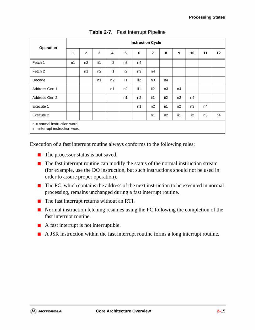
Processing States
Execution of a fast interrupt routine always conforms to the following rules:
The processor status is not saved.
The fast interrupt routine can modify the status of the normal instruction stream (for example, use the DO instruction, but such instructions should not be used in order to assure proper operation).
The PC, which contains the address of the next instruction to be executed in normal processing, remains unchanged during a fast interrupt routine.
The fast interrupt returns without an RTI.
Normal instruction fetching resumes using the PC following the completion of the fast interrupt routine.
A fast interrupt is not interruptible.
A JSR instruction within the fast interrupt routine forms a long interrupt routine.
Table 2-7. Fast Interrupt Pipeline
OperationInstruction Cycle
1 2 3 4 5 6 7 8 9 10 11 12
Fetch 1 n1 n2 ii1 ii2 n3 n4
Fetch 2 n1 n2 ii1 ii2 n3 n4
Decode n1 n2 ii1 ii2 n3 n4
Address Gen 1 n1 n2 ii1 ii2 n3 n4
Address Gen 2 n1 n2 ii1 ii2 n3 n4
Execute 1 n1 n2 ii1 ii2 n3 n4
Execute 2 n1 n2 ii1 ii2 n3 n4
n = normal instruction wordii = interrupt instruction word
Core Architecture Overview 2-15
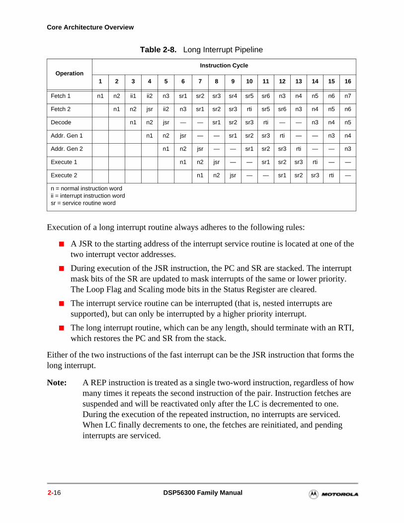
Core Architecture Overview
Execution of a long interrupt routine always adheres to the following rules:
A JSR to the starting address of the interrupt service routine is located at one of the two interrupt vector addresses.
During execution of the JSR instruction, the PC and SR are stacked. The interrupt mask bits of the SR are updated to mask interrupts of the same or lower priority. The Loop Flag and Scaling mode bits in the Status Register are cleared.
The interrupt service routine can be interrupted (that is, nested interrupts are supported), but can only be interrupted by a higher priority interrupt.
The long interrupt routine, which can be any length, should terminate with an RTI, which restores the PC and SR from the stack.
Either of the two instructions of the fast interrupt can be the JSR instruction that forms the long interrupt.
Note: A REP instruction is treated as a single two-word instruction, regardless of how many times it repeats the second instruction of the pair. Instruction fetches are suspended and will be reactivated only after the LC is decremented to one. During the execution of the repeated instruction, no interrupts are serviced. When LC finally decrements to one, the fetches are reinitiated, and pending interrupts are serviced.
Table 2-8. Long Interrupt Pipeline
OperationInstruction Cycle
1 2 3 4 5 6 7 8 9 10 11 12 13 14 15 16
Fetch 1 n1 n2 ii1 ii2 n3 sr1 sr2 sr3 sr4 sr5 sr6 n3 n4 n5 n6 n7
Fetch 2 n1 n2 jsr ii2 n3 sr1 sr2 sr3 rti sr5 sr6 n3 n4 n5 n6
Decode n1 n2 jsr — — sr1 sr2 sr3 rti — — n3 n4 n5
Addr. Gen 1 n1 n2 jsr — — sr1 sr2 sr3 rti — — n3 n4
Addr. Gen 2 n1 n2 jsr — — sr1 sr2 sr3 rti — — n3
Execute 1 n1 n2 jsr — — sr1 sr2 sr3 rti — —
Execute 2 n1 n2 jsr — — sr1 sr2 sr3 rti —
n = normal instruction wordii = interrupt instruction wordsr = service routine word
2-16 DSP56300 Family Manual
Processing States
and n
s.
If a non-interruptible code sequence is desired, change the IPL bits to the desired mask level. Due to pipelining, you will need four instructions before you can guarantee that the code is not interrupted by a maskable interrupt.
2.3.3 Reset Processing State
The DSP device enters reset processing state when the external RESET pin is asserted (a hardware reset). In the Reset state:
Internal peripheral devices are reset.
The modifier registers (M[0–7]) are set to $FFFFFF.
The interrupt priority registers are cleared.
The Bus Control Register (BCR), the Address Attribute Registers (AAR[3–0]) the DRAM Control Register (DCR) are set to their initial values as described iChapter 9, External Memory Interface (Port A). The initial value causes a maximum number of wait states to be added to every external memory acces
The Stack Pointer (SP) and the Stack Counter (SC) are cleared.
The following bits of the SR are cleared:
— Rounding mode (RM) bit (bit 21)
— Arithmetic Saturation mode (SM) bit (bit 20)
— Cache Enable (CE) bit (bit 19)
— Sixteen-bit Arithmetic (SA) mode bit (bit 17)
— DO Forever (FV) flag bit (bit 16)
— DO Loop Flag (LF) bit (bit 15)
— Double Precision Multiply (DM) mode bit (bit 14)
— Sixteen-bit Compatibility (SC) mode bit (bit 13)
— Scaling (S[1–0]) bits (bit 11 and bit 10)
— Condition Code bits (SR[7–0])
The following bits of the SR are set:
— Core Priority (CP[1–0]) bits (bit 23 and bit 22)
— Interrupt (I[1–0]) mask bits (bit 9 and bit 8)
The Instruction Cache Controller is initialized as described in Chapter 8, Instruction Cache.
The Cache Enable (CE) bit in SR and the Burst mode bit in OMR are cleared.
Core Architecture Overview 2-17
Core Architecture Overview
ress
AIT ed by
the e off. bled.
o the :
ding P
The PLL Control register is initialized as described in Chapter 6, PLL and Clock Generator.
The Vector Base Address Register (VBA) is cleared.
The DSP56300 core remains in the Reset state until RESET is deasserted. Upon leaving the Reset state, the Chip Operating mode bits of the OMR are loaded from the external mode select pins (MOD[A–D]), and program execution begins at the program memory addas described in Chapter 11, Operating Modes and Memory Spaces.
2.3.4 Wait Processing State
The Wait processing state is a low-power consumption state that occurs when the Winstruction executes. In the Wait state, the internal clock is disabled from all internalcircuitry except the internal peripherals. All internal processing halts until an unmaskinterrupt occurs, the DSP is reset, or DE is asserted. If the exit from Wait state is caused asserting DE, the processor enters the Debug mode.
2.3.5 Stop Processing State
The Stop processing state is the lowest power consumption mode that occurs whenSTOP instruction executes. In Stop mode, the clock oscillator activity depends on thPSTP bit in the PLL control register. If this bit is cleared, the clock oscillator is turnedIf the bit is set, the VCO remains active and the global clock to the entire chip is disaAll activity in the processor halts until one of the following actions occurs:
A low level is applied to the IRQA pin (IRQA asserted).
A low level is applied to the RESET pin (RESET asserted).
A low level is applied to the DE pin.
Any of these actions enables the oscillator. After a clock stabilization delay, clocks tprocessor and peripherals are re-enabled. If re-enabled, one of the following occurs
If the exit from Stop state was caused by a low level on the RESET pin, then the processor enters the Reset processing state.
If the exit from Stop state was caused by a low level on the IRQA pin, then the processor services the highest-priority pending interrupt. If no interrupt is pen(that is, IRQA was negated before interrupts were arbitrated), or if no interrupt isenabled, the processor resumes execution at the instruction following the STOinstruction that caused the entry into the Stop state.
If the exit from Stop state was caused by a low level on the DE pin, then the processor enters the Debug mode.
2-18 DSP56300 Family Manual
Processing States
For minimum power consumption during the Stop state at the cost of longer recovery time, clear the PSTP bit of the PLL Control Register. To enable rapid recovery when exiting the Stop state, at the cost of higher power consumption, set PSTP. PSTP is cleared by hardware reset.
2.3.6 Debug State
Debug state is invoked and used with the JTAG/OnCE port. See Chapter 7, Debugging Support for a description of the Debug state.
Core Architecture Overview 2-19

Core Architecture Overview
2-20 DSP56300 Family Manual
Chapter 3Data Arithmetic Logic Unit
3.1 Introduction
This section describes the architecture and the operation of the Data Arithmetic Logic Unit (Data ALU), the block where all the arithmetic and logical operations on data operands are performed.
3.2 Data ALU Architecture
The Data ALU contains the following components:
Four 24-bit input registers
A fully pipelined Multiplier-Accumulator (MAC)
Two 48-bit accumulator registers
Two 8-bit accumulator extension registers
A Bit Field Unit (BFU) with a 56-bit barrel shifter
An accumulator shifter
Two data bus shifter/limiter circuits
Figure 3-1 is a block diagram of the Data ALU.
DSP56300 Family Manual 3-1
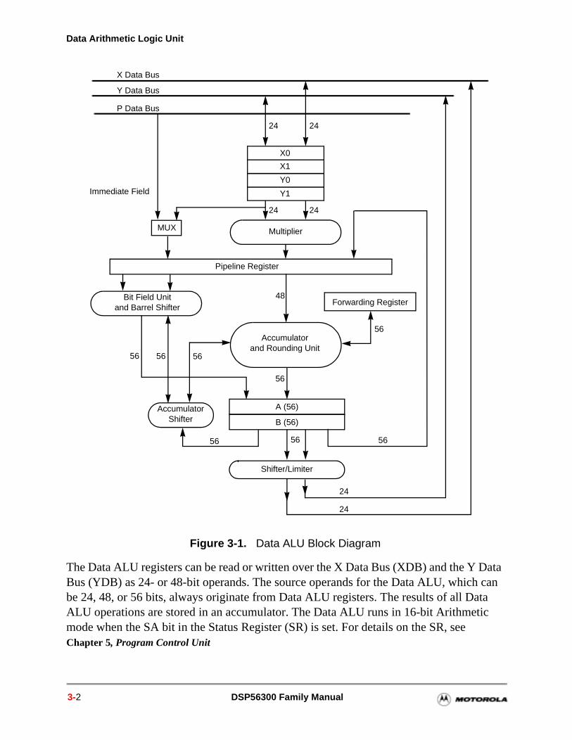
Data Arithmetic Logic Unit
The Data ALU registers can be read or written over the X Data Bus (XDB) and the Y Data Bus (YDB) as 24- or 48-bit operands. The source operands for the Data ALU, which can be 24, 48, or 56 bits, always originate from Data ALU registers. The results of all Data ALU operations are stored in an accumulator. The Data ALU runs in 16-bit Arithmetic mode when the SA bit in the Status Register (SR) is set. For details on the SR, see Chapter 5, Program Control Unit
Figure 3-1. Data ALU Block Diagram
Bit Field Unit and Barrel Shifter
AccumulatorShifter
Immediate Field
48
56
24
24
56
56
56
56
X Data Bus
Y Data Bus
2424
X0
X1
Y0
Y1
24 24
Multiplier
Accumulatorand Rounding Unit
A (56)
B (56)
Shifter/Limiter
Pipeline Register
P Data Bus
MUX
56
56
Forwarding Register
56
3-2 DSP56300 Family Manual
Data ALU Architecture
the clock
nts to ply be
he
the
All the Data ALU operations are performed in two clock cycles in pipeline fashion so that a new instruction can be initiated in every clock, yielding an effective execution rate of one instruction per clock cycle.
3.2.1 Data ALU Input Registers (X1, X0, Y1, Y0)
X1, X0, Y1, and Y0 are four 24-bit, general-purpose data registers. They can be treated as four independent 24-bit registers or as two 48-bit registers called X and Y, formed by concatenation of X1:X0 and Y1:Y0, respectively. X1 is the most significant word in X, and Y1 is the most significant word in Y. The registers serve as input buffers between the X Data Bus (XDB) or Y Data Bus (YDB) and the MAC unit or barrel shifter. They are used as Data ALU source operands, allowing new operands to be loaded for the next instruction while the current contents are used by the current instruction. The registers can also be read back out to the appropriate data bus.
3.2.2 Multiplier-Accumulator (MAC) Unit
The Multiplier-Accumulator (MAC) unit is the main arithmetic processing unit of the DSP56300 core. It accepts up to three input operands and outputs one 56-bit result of the following form:
Extension:Most Significant Product:Least Significant Product (EXT:MSP:LSP)
The operation of the MAC unit occurs independently and in parallel with XDB and YDB activity, and its registers facilitate buffering for both Data ALU inputs and outputs. Latches on the MAC unit input permit writing new data to an input register while the Data ALU processes the current data. The input to the multiplier can come only from the X or Y registers. The multiplier executes 24-bit x 24-bit, parallel fractional multiplies, between two’s-complement signed, unsigned, or mixed operands. The 48-bit product is right-justified into 56 bits and added to the 56-bit contents of either the A or B accumulator.
The 56-bit sum is stored back in the same accumulator. The multiply/accumulate operation is fully pipelined and takes two clock cycles to complete. In the first clock multiply is performed and the product is stored in the pipeline register. In the second the accumulator is added or subtracted. If a multiply without accumulation (MPY) is specified in the instruction, the MAC clears the accumulator and then adds the contethe product. When a 56-bit result is to be stored as a 24-bit operand, the LSP can simtruncated, or it can be rounded into the MSP. Rounding is performed if specified in tDSP instruction, for example, in the signed multiply-accumulate and round (MACR) instruction; the rounding is either convergent rounding (round-to-nearest-even) or two’s-complement rounding. The type of rounding is specified by the rounding bit in
Data Arithmetic Logic Unit 3-3
Data Arithmetic Logic Unit
into n. It is
ode
tored . If or
d re B or and r
bit
ister the sfer
and
ter is
Status Register (SR). The bit in the accumulator that is rounded is specified by the scaling mode bits in the SR.
The arithmetic unit’s result going into the accumulator can be saturated so that it fits48 bits (MSP and LSP). This process is commonly referred to as arithmetic saturatioactivated by the Arithmetic Saturation Mode (SM) bit in the SR. The purpose of this mis to provide for algorithms that do not recognize or cannot take advantage of the extension accumulator (EXT). For details, refer to Section 3.3.3, Arithmetic Saturation Mode, on page 3-11.
3.2.3 Data ALU Accumulator Registers (A2, A1, A0, B2, B1, B0)
The six Data ALU registers (A2, A1, A0, B2, B1, and B0) form two general-purpose,56-bit accumulators, A and B. Each of these two accumulators consists of three concatenated registers (A2:A1:A0 and B2:B1:B0, respectively). The 24-bit MSP is sin A1 or B1; the 24-bit LSP is stored in A0 or B0. The 8-bit EXT is stored in A2 or B2an ALU operation results in overflow into A2 (or B2), reading the A (or B) accumulatover the XDB or YDB substitutes a limiting constant in place of the value in the accumulator. The content of A or B is not affected if limiting occurs; only the value transferred over the XDB or YDB is limited. This process is commonly referred to astransfer saturation and should not be confused with the Arithmetic Saturation mode.
The overflow protection is performed after the contents of the accumulator are shifteaccording to the Scaling mode. Shifting and limiting is performed only when the enti56-bit A or B register is specified as the source for a parallel data move over the XDYDB. When A2, A1, A0, B2, B1, or B0 is the source for a parallel data move, shiftinglimiting are not performed. When the 8-bit wide accumulator extension register (A2 oB2) is the source for a parallel data move, it is sign-extended to produce the full 24-wide word. The accumulator registers (A or B) serve as buffer registers between thearithmetic unit and the XDB and/or YDB. These registers are used as both Data ALUsource and destination operands.
Automatic sign extension of the 56-bit accumulators is provided when the A or B regis written with a smaller operand. Sign extension can occur when writing A or B fromXDB and/or YDB or with the results of certain Data ALU operations such as the TranConditionally (Tcc) or Transfer Data ALU Register (TFR) instructions. If a word operis to be written to an accumulator register (A or B), the Most Significant Product (MSP)—A1 or B1—of the accumulator is written with the word operand, the Least Significant Product (LSP)—A0 or B0—is zero-filled, and the Extended (EXT) portion—A2 or B2—is sign-extended from MSP. Long-word operands are written into the low-order portion, MSP:LSP, of the Accumulator Register, and the EXT portion is sign-extended from MSP. No sign extension is performed if an individual 24-bit regis
3-4 DSP56300 Family Manual
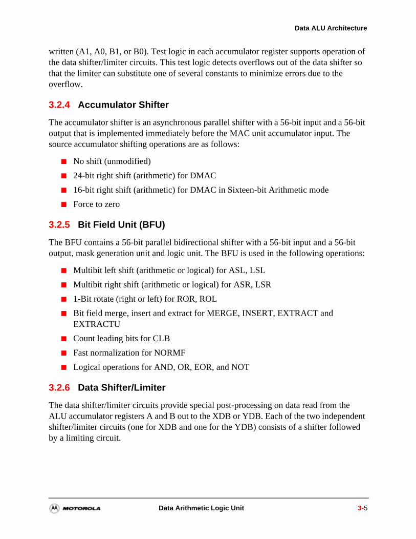
Data ALU Architecture
written (A1, A0, B1, or B0). Test logic in each accumulator register supports operation of the data shifter/limiter circuits. This test logic detects overflows out of the data shifter so that the limiter can substitute one of several constants to minimize errors due to the overflow.
3.2.4 Accumulator Shifter
The accumulator shifter is an asynchronous parallel shifter with a 56-bit input and a 56-bit output that is implemented immediately before the MAC unit accumulator input. The source accumulator shifting operations are as follows:
No shift (unmodified)
24-bit right shift (arithmetic) for DMAC
16-bit right shift (arithmetic) for DMAC in Sixteen-bit Arithmetic mode
Force to zero
3.2.5 Bit Field Unit (BFU)
The BFU contains a 56-bit parallel bidirectional shifter with a 56-bit input and a 56-bit output, mask generation unit and logic unit. The BFU is used in the following operations:
Multibit left shift (arithmetic or logical) for ASL, LSL
Multibit right shift (arithmetic or logical) for ASR, LSR
1-Bit rotate (right or left) for ROR, ROL
Bit field merge, insert and extract for MERGE, INSERT, EXTRACT and EXTRACTU
Count leading bits for CLB
Fast normalization for NORMF
Logical operations for AND, OR, EOR, and NOT
3.2.6 Data Shifter/Limiter
The data shifter/limiter circuits provide special post-processing on data read from the ALU accumulator registers A and B out to the XDB or YDB. Each of the two independent shifter/limiter circuits (one for XDB and one for the YDB) consists of a shifter followed by a limiting circuit.
Data Arithmetic Logic Unit 3-5
Data Arithmetic Logic Unit
le, to be de
ts. ing d two n
in the use), lected size, ed)
t a
3.2.6.1 Scaling
The data shifters in the shifters/limiters unit can perform the following data shift operations:
Scale up—shift data one bit to the left
Scale down—shift data one bit to the right
No scaling—pass the data unshifted
Each data shifter has a 24-bit output with overflow indication. These shifters permit dynamic scaling of fixed-point data without modifying the program code. For exampthis permits block floating-point algorithms such as Fast Fourier Transforms (FFTs) implemented in a regular fashion. The data shifters are controlled by the Scaling Mobits (S0 and S1, bits 11 and 10) in the SR.
3.2.6.2 Limiting
In the DSP56300 core, the Data ALU accumulators A and B have eight extension biLimiting occurs when the extension bits are in use and either A or B is the source beread over XDB or YDB. The limiters in the DSP56300 core place a shifted and limitevalue on XDB or YDB without changing the contents of the A or B registers. Having limiters allows two-word operands to be limited independently in the same instructiocycle. The two data limiters can also be combined to form one 48-bit data limiter forlong-word operands.
If the contents of the selected source accumulator are represented without overflowdestination operand size (that is, signed integer portion of the accumulator is not in the data limiter is disabled, and the operand is not modified. If the contents of the sesource accumulator are not represented without overflow in the destination operandthe data limiter substitutes a limited data value having maximum magnitude (saturatand having the same sign as the source accumulator contents:
$7FFFFF for 24-bit positive numbers
$7FFFFF FFFFFF for 48-bit positive numbers
$800000 for 24-bit negative numbers
$800000 000000 for 48-bit negative numbers
This process is called transfer saturation. The value in the accumulator register is noshifted or limited and can be reused within the Data ALU. When limiting does occur,flag is set and latched in the SR.
3-6 DSP56300 Family Manual
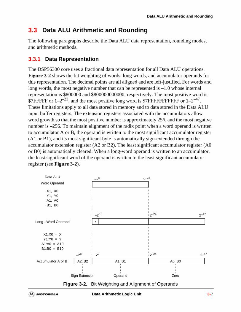
Data ALU Arithmetic and Rounding
al rd is
ritten ister
r (A0 tor, r
3.3 Data ALU Arithmetic and Rounding
The following paragraphs describe the Data ALU data representation, rounding modes, and arithmetic methods.
3.3.1 Data Representation
The DSP56300 core uses a fractional data representation for all Data ALU operations. Figure 3-2 shows the bit weighting of words, long words, and accumulator operands for this representation. The decimal points are all aligned and are left-justified. For words and long words, the most negative number that can be represented is –1.0 whose internrepresentation is $800000 and $800000000000, respectively. The most positive wo$7FFFFF or 1–2–23, and the most positive long word is $7FFFFFFFFFFF or 1–2–47. These limitations apply to all data stored in memory and to data stored in the Data ALU input buffer registers. The extension registers associated with the accumulators allow word growth so that the most positive number is approximately 256, and the most negative number is –256. To maintain alignment of the radix point when a word operand is wto accumulator A or B, the operand is written to the most significant accumulator reg(A1 or B1), and its most significant byte is automatically sign-extended through the accumulator extension register (A2 or B2). The least significant accumulator registeor B0) is automatically cleared. When a long-word operand is written to an accumulathe least significant word of the operand is written to the least significant accumulatoregister (see Figure 3-2).
Figure 3-2. Bit Weighting and Alignment of Operands
2–472–2420–28
2–472–24
–20 2–23
–20
Sign Extension Operand Zero
Data ALU
Word Operand
X1, X0Y1, Y0A1, A0B1, B0
Long - Word Operand
X1:X0 = XY1:Y0 = Y
A1:A0 = A10B1:B0 = B10
Accumulator A or B
*
A2, B2 A1, B1 A0, B0
Data Arithmetic Logic Unit 3-7
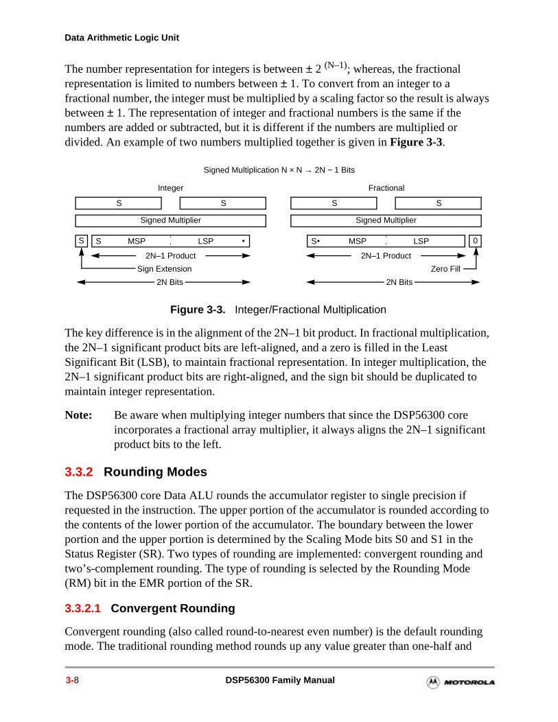
Data Arithmetic Logic Unit
he to
nt
f ing to er he and
ding nd
The number representation for integers is between ± 2 (N–1); whereas, the fractional representation is limited to numbers between ± 1. To convert from an integer to a fractional number, the integer must be multiplied by a scaling factor so the result is always between ± 1. The representation of integer and fractional numbers is the same if the numbers are added or subtracted, but it is different if the numbers are multiplied or divided. An example of two numbers multiplied together is given in Figure 3-3.
The key difference is in the alignment of the 2N–1 bit product. In fractional multiplication,the 2N–1 significant product bits are left-aligned, and a zero is filled in the Least Significant Bit (LSB), to maintain fractional representation. In integer multiplication, t2N–1 significant product bits are right-aligned, and the sign bit should be duplicatedmaintain integer representation.
Note: Be aware when multiplying integer numbers that since the DSP56300 coreincorporates a fractional array multiplier, it always aligns the 2N–1 significaproduct bits to the left.
3.3.2 Rounding Modes
The DSP56300 core Data ALU rounds the accumulator register to single precision irequested in the instruction. The upper portion of the accumulator is rounded accordthe contents of the lower portion of the accumulator. The boundary between the lowportion and the upper portion is determined by the Scaling Mode bits S0 and S1 in tStatus Register (SR). Two types of rounding are implemented: convergent roundingtwo’s-complement rounding. The type of rounding is selected by the Rounding Mode(RM) bit in the EMR portion of the SR.
3.3.2.1 Convergent Rounding
Convergent rounding (also called round-to-nearest even number) is the default rounmode. The traditional rounding method rounds up any value greater than one-half a
Figure 3-3. Integer/Fractional Multiplication
S S
Signed Multiplier
S
2N–1 Product
Sign Extension
2N Bits
S S
Signed Multiplier
0
2N–1 Product
Zero Fill
2N Bits
Integer Fractional
Signed Multiplication N × N → 2N − 1 Bits
S MSP LSP • S• MSP LSP
3-8 DSP56300 Family Manual
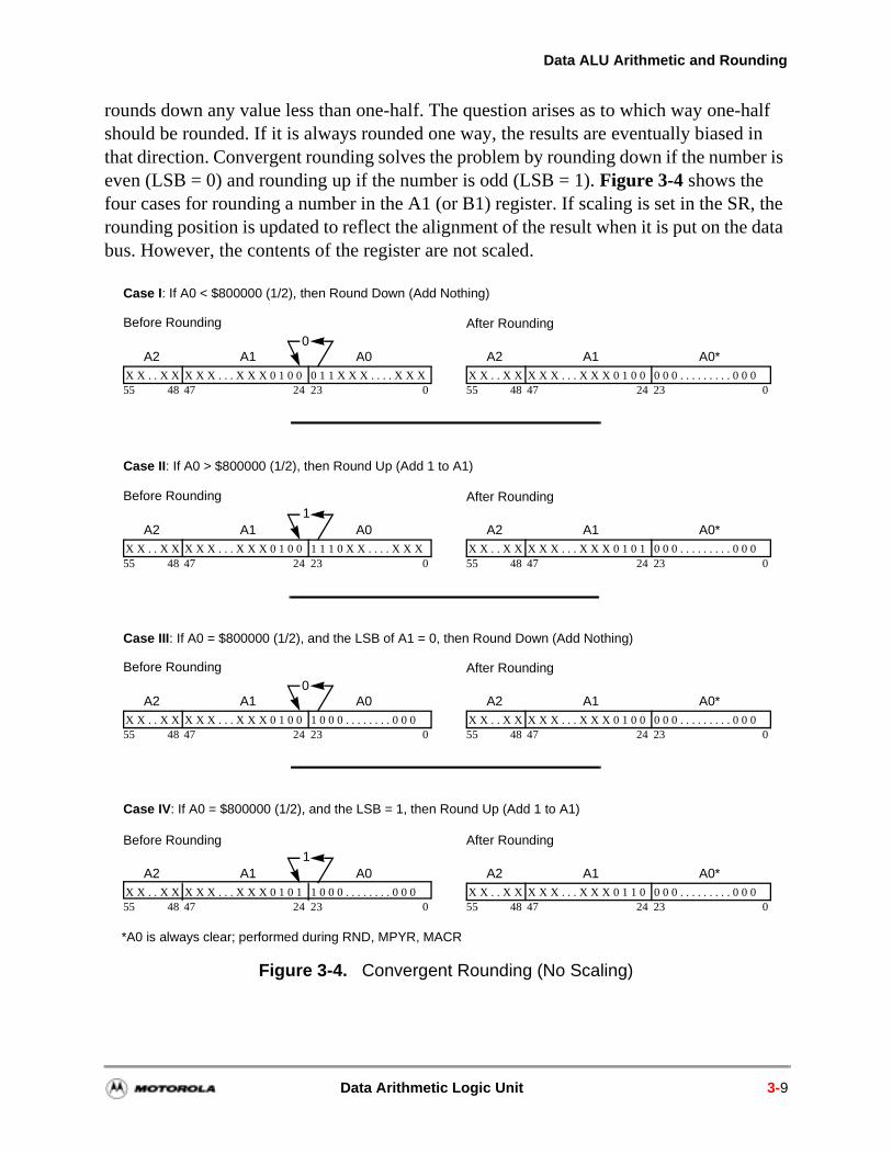
Data ALU Arithmetic and Rounding
rounds down any value less than one-half. The question arises as to which way one-half should be rounded. If it is always rounded one way, the results are eventually biased in that direction. Convergent rounding solves the problem by rounding down if the number is even (LSB = 0) and rounding up if the number is odd (LSB = 1). Figure 3-4 shows the four cases for rounding a number in the A1 (or B1) register. If scaling is set in the SR, the rounding position is updated to reflect the alignment of the result when it is put on the data bus. However, the contents of the register are not scaled.
Figure 3-4. Convergent Rounding (No Scaling)
Case I: If A0 < $800000 (1/2), then Round Down (Add Nothing)
Before Rounding After Rounding
Case II: If A0 > $800000 (1/2), then Round Up (Add 1 to A1)
Case III: If A0 = $800000 (1/2), and the LSB of A1 = 0, then Round Down (Add Nothing)
Case IV: If A0 = $800000 (1/2), and the LSB = 1, then Round Up (Add 1 to A1)
*A0 is always clear; performed during RND, MPYR, MACR
X X . . X X X X X . . . X X X 0 1 0 0 0 1 1 X X X . . . . X X X55 48 47 24 23 0
A2 A1 A00
X X . . X X X X X . . . X X X 0 1 0 0 0 0 0 . . . . . . . . . 0 0 055 48 47 24 23 0
A2 A1 A0*
Before Rounding After Rounding
X X . . X X X X X . . . X X X 0 1 0 0 1 1 1 0 X X . . . . X X X55 48 47 24 23 0
A2 A1 A01
X X . . X X X X X . . . X X X 0 1 0 1 0 0 0 . . . . . . . . . 0 0 055 48 47 24 23 0
A2 A1 A0*
Before Rounding After Rounding
X X . . X X X X X . . . X X X 0 1 0 0 1 0 0 0 . . . . . . . . 0 0 055 48 47 24 23 0
A2 A1 A00
X X . . X X X X X . . . X X X 0 1 0 0 0 0 0 . . . . . . . . . 0 0 055 48 47 24 23 0
A2 A1 A0*
Before Rounding After Rounding
X X . . X X X X X . . . X X X 0 1 0 1 1 0 0 0 . . . . . . . . 0 0 055 48 47 24 23 0
A2 A1 A01
X X . . X X X X X . . . X X X 0 1 1 0 0 0 0 . . . . . . . . . 0 0 055 48 47 24 23 0
A2 A1 A0*
Data Arithmetic Logic Unit 3-9
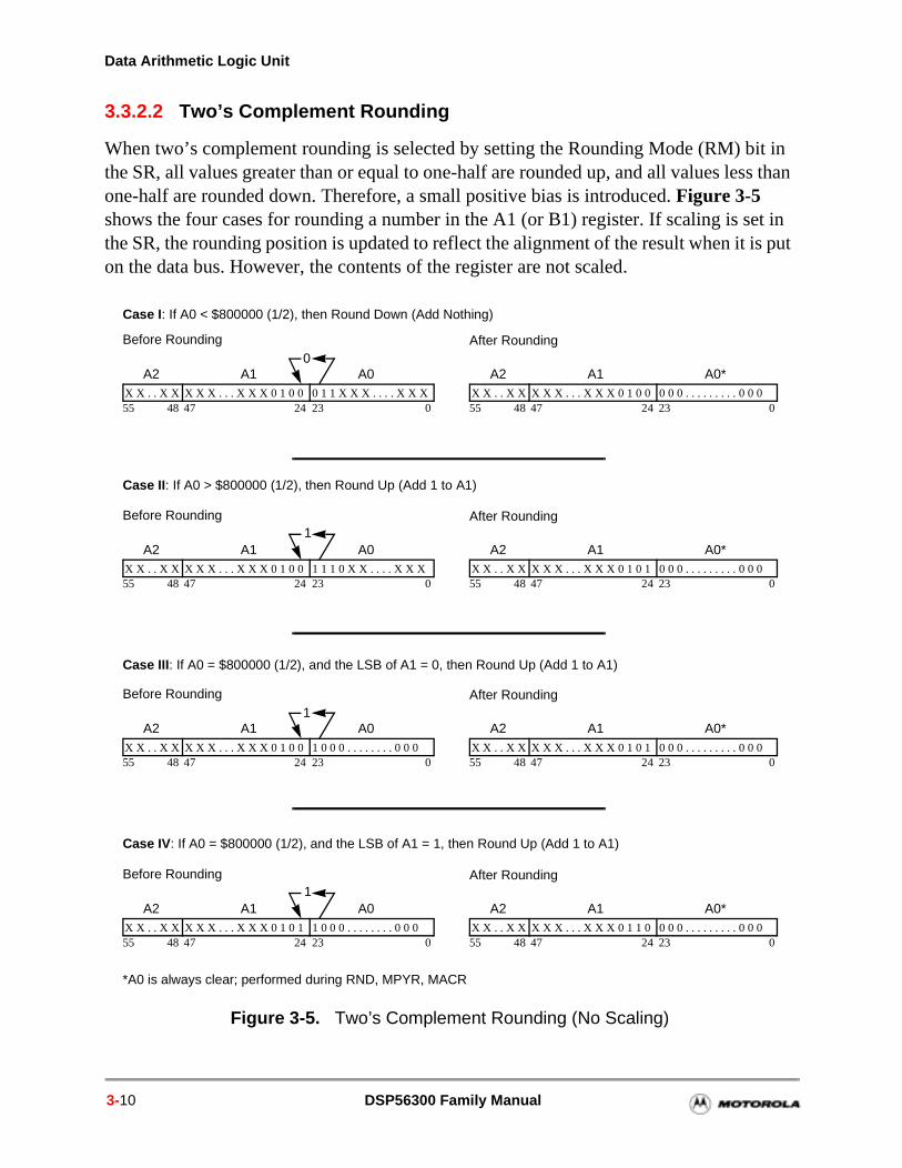
Data Arithmetic Logic Unit
it in ss than
et in is put
3.3.2.2 Two’s Complement Rounding
When two’s complement rounding is selected by setting the Rounding Mode (RM) bthe SR, all values greater than or equal to one-half are rounded up, and all values leone-half are rounded down. Therefore, a small positive bias is introduced. Figure 3-5 shows the four cases for rounding a number in the A1 (or B1) register. If scaling is sthe SR, the rounding position is updated to reflect the alignment of the result when it on the data bus. However, the contents of the register are not scaled.
Figure 3-5. Two’s Complement Rounding (No Scaling)
Case I: If A0 < $800000 (1/2), then Round Down (Add Nothing)
Before Rounding After Rounding
Case II: If A0 > $800000 (1/2), then Round Up (Add 1 to A1)
Case III: If A0 = $800000 (1/2), and the LSB of A1 = 0, then Round Up (Add 1 to A1)
Case IV: If A0 = $800000 (1/2), and the LSB of A1 = 1, then Round Up (Add 1 to A1)
*A0 is always clear; performed during RND, MPYR, MACR
X X . . X X X X X . . . X X X 0 1 0 0 0 1 1 X X X . . . . X X X55 48 47 24 23 0
A2 A1 A00
X X . . X X X X X . . . X X X 0 1 0 0 0 0 0 . . . . . . . . . 0 0 055 48 47 24 23 0
A2 A1 A0*
Before Rounding After Rounding
X X . . X X X X X . . . X X X 0 1 0 0 1 1 1 0 X X . . . . X X X55 48 47 24 23 0
A2 A1 A01
X X . . X X X X X . . . X X X 0 1 0 1 0 0 0 . . . . . . . . . 0 0 055 48 47 24 23 0
A2 A1 A0*
Before Rounding After Rounding
X X . . X X X X X . . . X X X 0 1 0 0 1 0 0 0 . . . . . . . . 0 0 055 48 47 24 23 0
A2 A1 A01
X X . . X X X X X . . . X X X 0 1 0 1 0 0 0 . . . . . . . . . 0 0 055 48 47 24 23 0
A2 A1 A0*
Before Rounding After Rounding
X X . . X X X X X . . . X X X 0 1 0 1 1 0 0 0 . . . . . . . . 0 0 055 48 47 24 23 0
A2 A1 A01
X X . . X X X X X . . . X X X 0 1 1 0 0 0 0 . . . . . . . . . 0 0 055 48 47 24 23 0
A2 A1 A0*
3-10 DSP56300 Family Manual
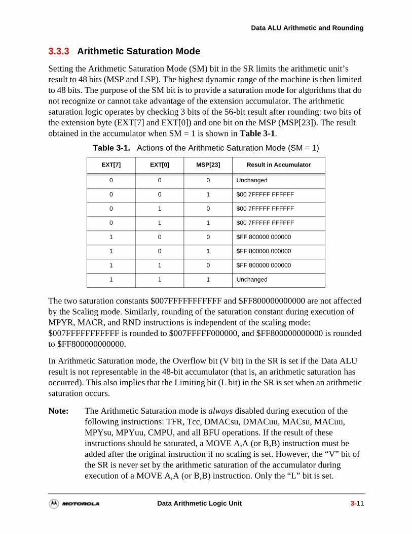
Data ALU Arithmetic and Rounding
mited at do ic its of ult
ffected of
unded
U has etic
of
3.3.3 Arithmetic Saturation Mode
Setting the Arithmetic Saturation Mode (SM) bit in the SR limits the arithmetic unit’s result to 48 bits (MSP and LSP). The highest dynamic range of the machine is then lito 48 bits. The purpose of the SM bit is to provide a saturation mode for algorithms thnot recognize or cannot take advantage of the extension accumulator. The arithmetsaturation logic operates by checking 3 bits of the 56-bit result after rounding: two bthe extension byte (EXT[7] and EXT[0]) and one bit on the MSP (MSP[23]). The resobtained in the accumulator when SM = 1 is shown in Table 3-1.
The two saturation constants $007FFFFFFFFFFF and $FF800000000000 are not aby the Scaling mode. Similarly, rounding of the saturation constant during executionMPYR, MACR, and RND instructions is independent of the scaling mode: $007FFFFFFFFFFF is rounded to $007FFFFF000000, and $FF800000000000 is roto $FF800000000000.
In Arithmetic Saturation mode, the Overflow bit (V bit) in the SR is set if the Data ALresult is not representable in the 48-bit accumulator (that is, an arithmetic saturationoccurred). This also implies that the Limiting bit (L bit) in the SR is set when an arithmsaturation occurs.
Note: The Arithmetic Saturation mode is always disabled during execution of the following instructions: TFR, Tcc, DMACsu, DMACuu, MACsu, MACuu, MPYsu, MPYuu, CMPU, and all BFU operations. If the result of these instructions should be saturated, a MOVE A,A (or B,B) instruction must beadded after the original instruction if no scaling is set. However, the “V” bitthe SR is never set by the arithmetic saturation of the accumulator during execution of a MOVE A,A (or B,B) instruction. Only the “L” bit is set.
Table 3-1. Actions of the Arithmetic Saturation Mode (SM = 1)
EXT[7] EXT[0] MSP[23] Result in Accumulator
0 0 0 Unchanged
0 0 1 $00 7FFFFF FFFFFF
0 1 0 $00 7FFFFF FFFFFF
0 1 1 $00 7FFFFF FFFFFF
1 0 0 $FF 800000 000000
1 0 1 $FF 800000 000000
1 1 0 $FF 800000 000000
1 1 1 Unchanged
Data Arithmetic Logic Unit 3-11
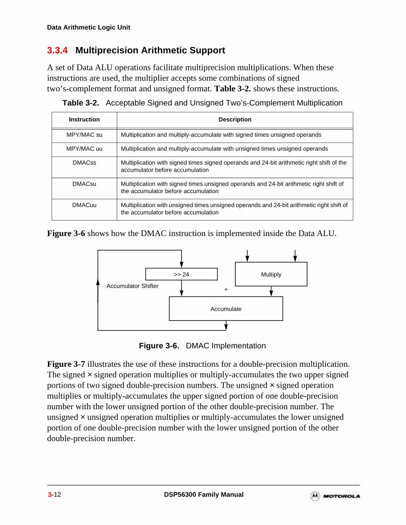
Data Arithmetic Logic Unit
n. d
3.3.4 Multiprecision Arithmetic Support
A set of Data ALU operations facilitate multiprecision multiplications. When these instructions are used, the multiplier accepts some combinations of signed two’s-complement format and unsigned format. Table 3-2. shows these instructions.
Figure 3-6 shows how the DMAC instruction is implemented inside the Data ALU.
Figure 3-7 illustrates the use of these instructions for a double-precision multiplicatioThe signed × signed operation multiplies or multiply-accumulates the two upper signeportions of two signed double-precision numbers. The unsigned × signed operation multiplies or multiply-accumulates the upper signed portion of one double-precision number with the lower unsigned portion of the other double-precision number. The unsigned × unsigned operation multiplies or multiply-accumulates the lower unsignedportion of one double-precision number with the lower unsigned portion of the otherdouble-precision number.
Table 3-2. Acceptable Signed and Unsigned Two’s-Complement Multiplication
Instruction Description
MPY/MAC su Multiplication and multiply-accumulate with signed times unsigned operands
MPY/MAC uu Multiplication and multiply-accumulate with unsigned times unsigned operands
DMACss Multiplication with signed times signed operands and 24-bit arithmetic right shift of the accumulator before accumulation
DMACsu Multiplication with signed times unsigned operands and 24-bit arithmetic right shift of the accumulator before accumulation
DMACuu Multiplication with unsigned times unsigned operands and 24-bit arithmetic right shift of the accumulator before accumulation
Figure 3-6. DMAC Implementation
Multiply
+
Accumulate
Accumulator Shifter
>> 24
3-12 DSP56300 Family Manual
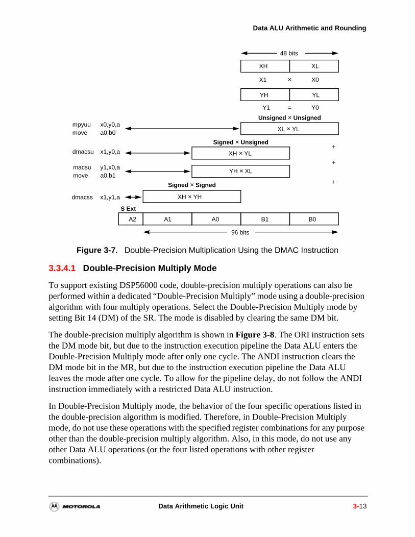
Data ALU Arithmetic and Rounding
ion y
he e
DI
in
urpose y
Figure 3-7. Double-Precision Multiplication Using the DMAC Instruction
3.3.4.1 Double-Precision Multiply Mode
To support existing DSP56000 code, double-precision multiply operations can also be performed within a dedicated “Double-Precision Multiply” mode using a double-precisalgorithm with four multiply operations. Select the Double-Precision Multiply mode bsetting Bit 14 (DM) of the SR. The mode is disabled by clearing the same DM bit.
The double-precision multiply algorithm is shown in Figure 3-8. The ORI instruction setsthe DM mode bit, but due to the instruction execution pipeline the Data ALU enters tDouble-Precision Multiply mode after only one cycle. The ANDI instruction clears thDM mode bit in the MR, but due to the instruction execution pipeline the Data ALU leaves the mode after one cycle. To allow for the pipeline delay, do not follow the ANinstruction immediately with a restricted Data ALU instruction.
In Double-Precision Multiply mode, the behavior of the four specific operations listedthe double-precision algorithm is modified. Therefore, in Double-Precision Multiply mode, do not use these operations with the specified register combinations for any pother than the double-precision multiply algorithm. Also, in this mode, do not use another Data ALU operations (or the four listed operations with other register combinations).
48 bits
96 bits
B0B1A0A1A2
X0X1
Y1 Y0
XLXH
YH YL
×
=
S Ext
+
+
+
XL × YL
XH × YL
YH × XL
XH × YH
Signed × Unsigned
Signed × Signed
Unsigned × Unsignedx0,y0,aa0,b0
x1,y0,a
y1,x0,aa0,b1
x1,y1,a
mpyuumove
dmacsu
macsumove
dmacss
Data Arithmetic Logic Unit 3-13
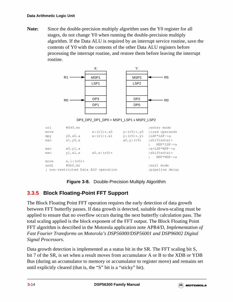
Data Arithmetic Logic Unit
l
Note: Since the double-precision multiply algorithm uses the Y0 register for all stages, do not change Y0 when running the double-precision multiply algorithm. If the Data ALU is required by an interrupt service routine, save the contents of Y0 with the contents of the other Data ALU registers before processing the interrupt routine, and restore them before leaving the interrupt routine.
3.3.5 Block Floating-Point FFT Support
The Block Floating Point FFT operation requires the early detection of data growth between FFT butterfly passes. If data growth is detected, suitable down-scaling must be applied to ensure that no overflow occurs during the next butterfly calculation pass. The total scaling applied is the block exponent of the FFT output. The Block Floating Point FFT algorithm is described in the Motorola application note APR4/D, Implementation of Fast Fourier Transforms on Motorola’s DSP56000/DSP56001 and DSP96002 DigitaSignal Processors.
Data growth detection is implemented as a status bit in the SR. The FFT scaling bit S, bit 7 of the SR, is set when a result moves from accumulator A or B to the XDB or YDB Bus (during an accumulator to memory or accumulator to register move) and remains set until explicitly cleared (that is, the “S” bit is a “sticky” bit).
Figure 3-8. Double-Precision Multiply Algorithm
Y:X:
R5MSP2
LSP2
MSP1
LSP1
R1
DP2
DP0
DP3
DP1R0R0
DP3_DP2_DP1_DP0 = MSP1_LSP1 x MSP2_LSP2
ori #$40,mr ;enter modemove x:(r1)+,x0 y:(r5)+,y0 ;load operandsmpy y0,x0,a x:(r1)+,x1 y:(r5)+,y1 ;LSP*LSP->amac x1,y0,a a0,y:(r0) ;shifted(a)+
; MSP*LSP->amac x0,y1,a ;a+LSP*MSP->amac y1,x1,a a0,x:(r0)+ ;shifted(a)+
; MSP*MSP->amove a,l:(r0)+andi #$bf,mr ;exit mode; non-restricted Data ALU operation ;pipeline delay
3-14 DSP56300 Family Manual
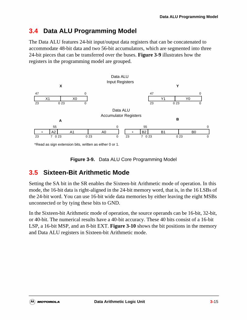
Data ALU Programming Model
3.4 Data ALU Programming Model
The Data ALU features 24-bit input/output data registers that can be concatenated to accommodate 48-bit data and two 56-bit accumulators, which are segmented into three 24-bit pieces that can be transferred over the buses. Figure 3-9 illustrates how the registers in the programming model are grouped.
Figure 3-9. Data ALU Core Programming Model
3.5 Sixteen-Bit Arithmetic Mode
Setting the SA bit in the SR enables the Sixteen-bit Arithmetic mode of operation. In this mode, the 16-bit data is right-aligned in the 24-bit memory word, that is, in the 16 LSBs of the 24-bit word. You can use 16-bit wide data memories by either leaving the eight MSBs unconnected or by tying these bits to GND.
In the Sixteen-bit Arithmetic mode of operation, the source operands can be 16-bit, 32-bit, or 40-bit. The numerical results have a 40-bit accuracy. These 40 bits consist of a 16-bit LSP, a 16-bit MSP, and an 8-bit EXT. Figure 3-10 shows the bit positions in the memory and Data ALU registers in Sixteen-bit Arithmetic mode.
Data ALU
Data ALU
* A2 A1 A0
Input Registers
Accumulator Registers
*Read as sign extension bits, written as either 0 or 1.
X Y
A B
X1 X0
* B2 B1 B0
Y1 Y0
47
23
0
00 23
47
23
0
00 23
55
23
0
00 230723
55
23
0
00 230723
Data Arithmetic Logic Unit 3-15
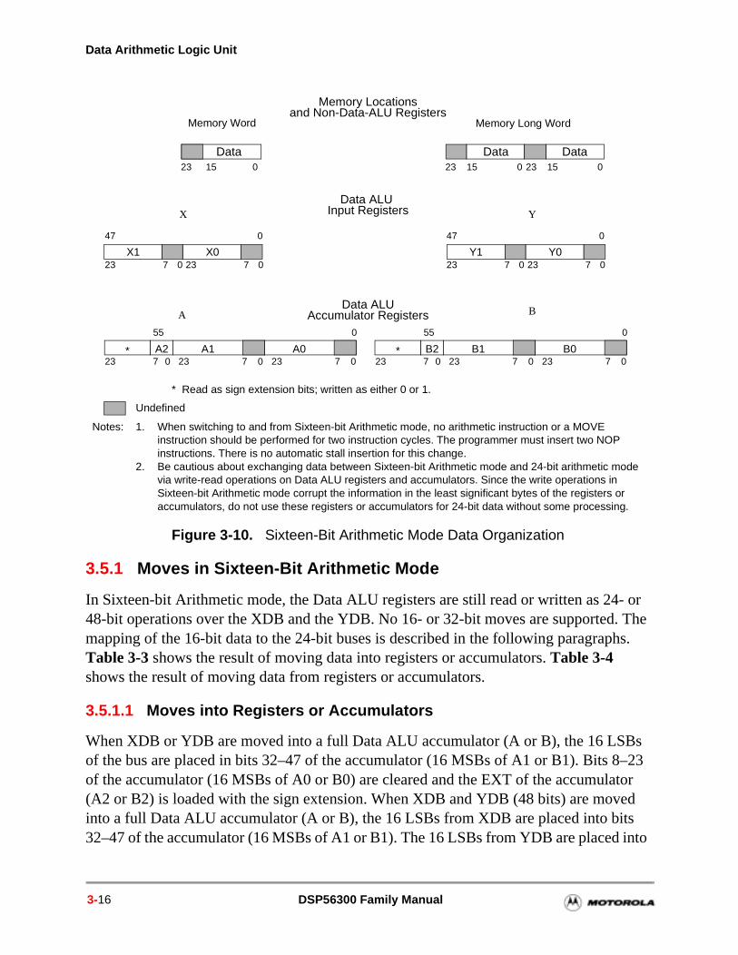
Data Arithmetic Logic Unit
–23 tor ed s into
3.5.1 Moves in Sixteen-Bit Arithmetic Mode
In Sixteen-bit Arithmetic mode, the Data ALU registers are still read or written as 24- or 48-bit operations over the XDB and the YDB. No 16- or 32-bit moves are supported. The mapping of the 16-bit data to the 24-bit buses is described in the following paragraphs. Table 3-3 shows the result of moving data into registers or accumulators. Table 3-4 shows the result of moving data from registers or accumulators.
3.5.1.1 Moves into Registers or Accumulators
When XDB or YDB are moved into a full Data ALU accumulator (A or B), the 16 LSBs of the bus are placed in bits 32–47 of the accumulator (16 MSBs of A1 or B1). Bits 8of the accumulator (16 MSBs of A0 or B0) are cleared and the EXT of the accumula(A2 or B2) is loaded with the sign extension. When XDB and YDB (48 bits) are movinto a full Data ALU accumulator (A or B), the 16 LSBs from XDB are placed into bit32–47 of the accumulator (16 MSBs of A1 or B1). The 16 LSBs from YDB are placed
Figure 3-10. Sixteen-Bit Arithmetic Mode Data Organization
Data ALU
Data ALU
* A2 A1 A0
Input Registers
Accumulator Registers
* Read as sign extension bits; written as either 0 or 1.
X Y
A B
X1 X0
Undefined
* B2 B1 B0
Y1 Y0
Memory Locations
Memory Word Memory Long Wordand Non-Data-ALU Registers
Notes: 1. When switching to and from Sixteen-bit Arithmetic mode, no arithmetic instruction or a MOVE instruction should be performed for two instruction cycles. The programmer must insert two NOP instructions. There is no automatic stall insertion for this change.
2. Be cautious about exchanging data between Sixteen-bit Arithmetic mode and 24-bit arithmetic mode via write-read operations on Data ALU registers and accumulators. Since the write operations in Sixteen-bit Arithmetic mode corrupt the information in the least significant bytes of the registers or accumulators, do not use these registers or accumulators for 24-bit data without some processing.
Data Data Data23 15 0 23 15 0 23 15 0
47 0
23 7 0 23 7 0
47 0
23 7 0 23 7 0
55 0
23 7 0 23 7 0 23 7 0
55 0
23 7 0 23 7 0 23 7 0
3-16 DSP56300 Family Manual
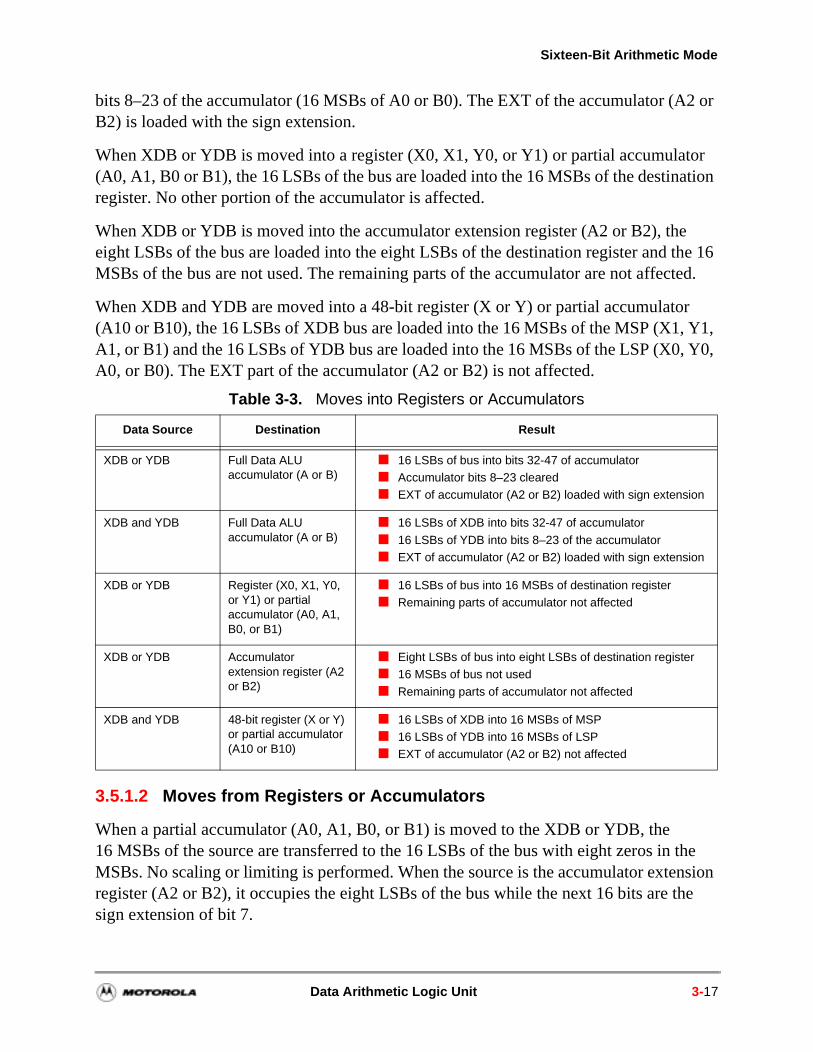
Sixteen-Bit Arithmetic Mode
2 or
r ation
the 16 ted.
Y1, , Y0,
the sion
he
bits 8–23 of the accumulator (16 MSBs of A0 or B0). The EXT of the accumulator (AB2) is loaded with the sign extension.
When XDB or YDB is moved into a register (X0, X1, Y0, or Y1) or partial accumulato(A0, A1, B0 or B1), the 16 LSBs of the bus are loaded into the 16 MSBs of the destinregister. No other portion of the accumulator is affected.
When XDB or YDB is moved into the accumulator extension register (A2 or B2), theeight LSBs of the bus are loaded into the eight LSBs of the destination register and MSBs of the bus are not used. The remaining parts of the accumulator are not affec
When XDB and YDB are moved into a 48-bit register (X or Y) or partial accumulator(A10 or B10), the 16 LSBs of XDB bus are loaded into the 16 MSBs of the MSP (X1,A1, or B1) and the 16 LSBs of YDB bus are loaded into the 16 MSBs of the LSP (X0A0, or B0). The EXT part of the accumulator (A2 or B2) is not affected.
3.5.1.2 Moves from Registers or Accumulators
When a partial accumulator (A0, A1, B0, or B1) is moved to the XDB or YDB, the 16 MSBs of the source are transferred to the 16 LSBs of the bus with eight zeros in MSBs. No scaling or limiting is performed. When the source is the accumulator extenregister (A2 or B2), it occupies the eight LSBs of the bus while the next 16 bits are tsign extension of bit 7.
Table 3-3. Moves into Registers or Accumulators
Data Source Destination Result
XDB or YDB Full Data ALU accumulator (A or B)
16 LSBs of bus into bits 32-47 of accumulator Accumulator bits 8–23 cleared EXT of accumulator (A2 or B2) loaded with sign extension
XDB and YDB Full Data ALU accumulator (A or B)
16 LSBs of XDB into bits 32-47 of accumulator
16 LSBs of YDB into bits 8–23 of the accumulator EXT of accumulator (A2 or B2) loaded with sign extension
XDB or YDB Register (X0, X1, Y0, or Y1) or partial accumulator (A0, A1, B0, or B1)
16 LSBs of bus into 16 MSBs of destination register Remaining parts of accumulator not affected
XDB or YDB Accumulator extension register (A2 or B2)
Eight LSBs of bus into eight LSBs of destination register 16 MSBs of bus not used
Remaining parts of accumulator not affected
XDB and YDB 48-bit register (X or Y) or partial accumulator (A10 or B10)
16 LSBs of XDB into 16 MSBs of MSP 16 LSBs of YDB into 16 MSBs of LSP EXT of accumulator (A2 or B2) not affected
Data Arithmetic Logic Unit 3-17
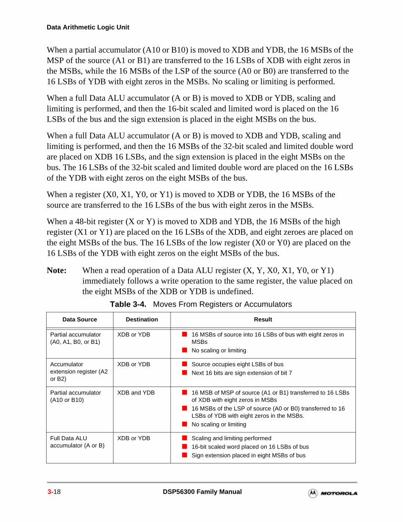
Data Arithmetic Logic Unit
When a partial accumulator (A10 or B10) is moved to XDB and YDB, the 16 MSBs of the MSP of the source (A1 or B1) are transferred to the 16 LSBs of XDB with eight zeros in the MSBs, while the 16 MSBs of the LSP of the source (A0 or B0) are transferred to the 16 LSBs of YDB with eight zeros in the MSBs. No scaling or limiting is performed.
When a full Data ALU accumulator (A or B) is moved to XDB or YDB, scaling and limiting is performed, and then the 16-bit scaled and limited word is placed on the 16 LSBs of the bus and the sign extension is placed in the eight MSBs on the bus.
When a full Data ALU accumulator (A or B) is moved to XDB and YDB, scaling and limiting is performed, and then the 16 MSBs of the 32-bit scaled and limited double word are placed on XDB 16 LSBs, and the sign extension is placed in the eight MSBs on the bus. The 16 LSBs of the 32-bit scaled and limited double word are placed on the 16 LSBs of the YDB with eight zeros on the eight MSBs of the bus.
When a register (X0, X1, Y0, or Y1) is moved to XDB or YDB, the 16 MSBs of the source are transferred to the 16 LSBs of the bus with eight zeros in the MSBs.
When a 48-bit register (X or Y) is moved to XDB and YDB, the 16 MSBs of the high register (X1 or Y1) are placed on the 16 LSBs of the XDB, and eight zeroes are placed on the eight MSBs of the bus. The 16 LSBs of the low register (X0 or Y0) are placed on the 16 LSBs of the YDB with eight zeros on the eight MSBs of the bus.
Note: When a read operation of a Data ALU register (X, Y, X0, X1, Y0, or Y1) immediately follows a write operation to the same register, the value placed on the eight MSBs of the XDB or YDB is undefined.
Table 3-4. Moves From Registers or Accumulators
Data Source Destination Result
Partial accumulator (A0, A1, B0, or B1)
XDB or YDB 16 MSBs of source into 16 LSBs of bus with eight zeros in MSBs
No scaling or limiting
Accumulator extension register (A2 or B2)
XDB or YDB Source occupies eight LSBs of bus
Next 16 bits are sign extension of bit 7
Partial accumulator (A10 or B10)
XDB and YDB 16 MSB of MSP of source (A1 or B1) transferred to 16 LSBs of XDB with eight zeros in MSBs
16 MSBs of the LSP of source (A0 or B0) transferred to 16 LSBs of YDB with eight zeros in the MSBs.
No scaling or limiting
Full Data ALU accumulator (A or B)
XDB or YDB Scaling and limiting performed 16-bit scaled word placed on 16 LSBs of bus Sign extension placed in eight MSBs of bus
3-18 DSP56300 Family Manual
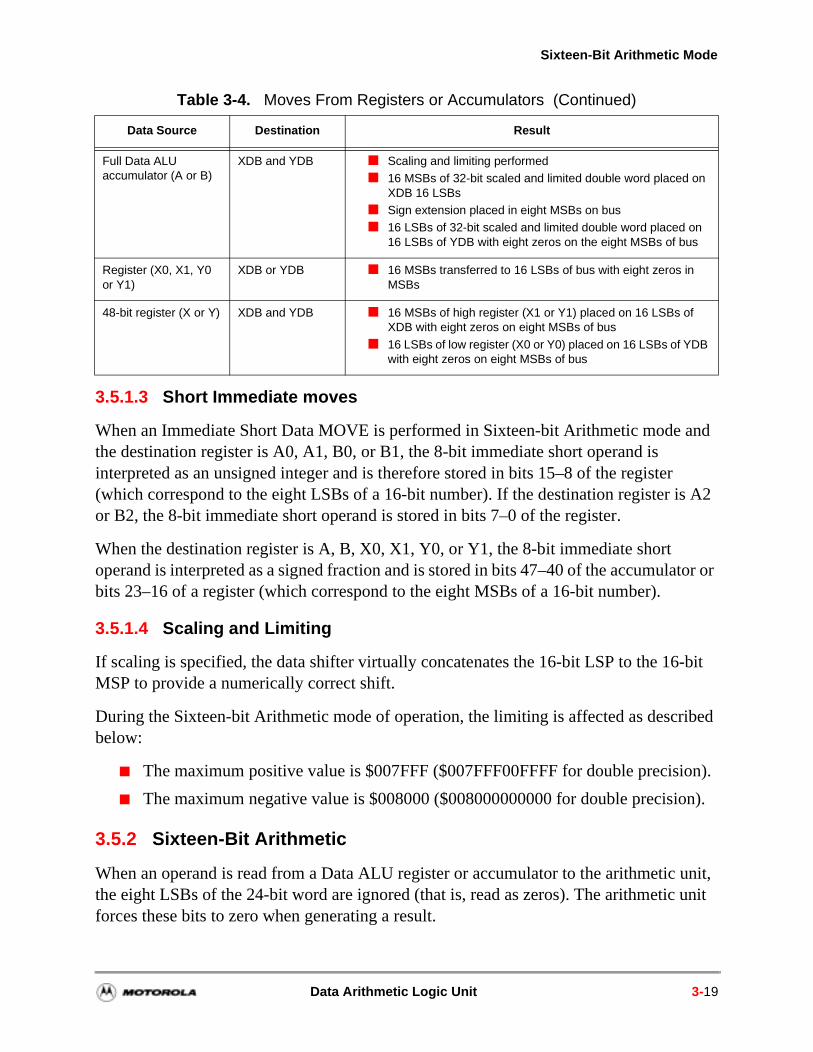
Sixteen-Bit Arithmetic Mode
r s A2
ator or
-bit
ibed
on).
n).
unit, unit
3.5.1.3 Short Immediate moves
When an Immediate Short Data MOVE is performed in Sixteen-bit Arithmetic mode and the destination register is A0, A1, B0, or B1, the 8-bit immediate short operand is interpreted as an unsigned integer and is therefore stored in bits 15–8 of the registe(which correspond to the eight LSBs of a 16-bit number). If the destination register ior B2, the 8-bit immediate short operand is stored in bits 7–0 of the register.
When the destination register is A, B, X0, X1, Y0, or Y1, the 8-bit immediate short operand is interpreted as a signed fraction and is stored in bits 47–40 of the accumulbits 23–16 of a register (which correspond to the eight MSBs of a 16-bit number).
3.5.1.4 Scaling and Limiting
If scaling is specified, the data shifter virtually concatenates the 16-bit LSP to the 16MSP to provide a numerically correct shift.
During the Sixteen-bit Arithmetic mode of operation, the limiting is affected as descrbelow:
The maximum positive value is $007FFF ($007FFF00FFFF for double precisi
The maximum negative value is $008000 ($008000000000 for double precisio
3.5.2 Sixteen-Bit Arithmetic
When an operand is read from a Data ALU register or accumulator to the arithmeticthe eight LSBs of the 24-bit word are ignored (that is, read as zeros). The arithmeticforces these bits to zero when generating a result.
Full Data ALU accumulator (A or B)
XDB and YDB Scaling and limiting performed 16 MSBs of 32-bit scaled and limited double word placed on
XDB 16 LSBs Sign extension placed in eight MSBs on bus 16 LSBs of 32-bit scaled and limited double word placed on
16 LSBs of YDB with eight zeros on the eight MSBs of bus
Register (X0, X1, Y0 or Y1)
XDB or YDB 16 MSBs transferred to 16 LSBs of bus with eight zeros in MSBs
48-bit register (X or Y) XDB and YDB 16 MSBs of high register (X1 or Y1) placed on 16 LSBs of XDB with eight zeros on eight MSBs of bus
16 LSBs of low register (X0 or Y0) placed on 16 LSBs of YDB with eight zeros on eight MSBs of bus
Table 3-4. Moves From Registers or Accumulators (Continued)
Data Source Destination Result
Data Arithmetic Logic Unit 3-19

Data Arithmetic Logic Unit
The arithmetic unit virtually concatenates the 16-bit LSP with the 16-bit MSP to form a continuous number. Therefore, all arithmetic operations, including shifts, are numerically correct. The execution of Data ALU instructions in Sixteen-bit Arithmetic mode is not affected, except for the following:
The operand and result widths are 16/32/40 instead of 24/48/56.
The rounding, if specified by the operation, is performed on the Most Significant Bit of the 16-bit Least Significant Portion (LSP) of the result, that is on the bit corresponding to bit 23 of A0/B0 (the Scaling mode affects this position accordingly). See the RND instruction in Chapter 13, Instruction Set for details.
The arithmetic saturation detection is unchanged, but the saturated values change to $007FFF00FFFF00 and $FF800000000000.
In ADC/SBC instructions, the Carry bit C is added/subtracted to the LSB of the 16-bit LSP.
Logic operations affect only the 16-bit wide word.
Rotation in rotate instructions is performed on a 16-bit wide word.
The possible normalization range changes, thus affecting the CLB instruction.
The DMAC instruction performs a 16-bit arithmetic right shift of the accumulator before accumulation.
The double-precision multiplication algorithm is not supported, even if the Double-Precision Multiply mode bit is set.
The bit parsing instructions (MERGE, EXTRACT, EXTRACTU, and INSERT) are modified by the Sixteen-bit Arithmetic mode to perform on the appropriate bit positions of the 16-bit data. For the INSERT instruction, you must update the offset by adding a bias value of 16. Refer to Chapter 13, Instruction Set for details on specific instructions.
In the read-modify-write instructions (BCHG, BCLR, BSET and BTST) and in the Jump/Branch on bit instructions (BRCLR, BRSET, BSCLR, BSSET, JCLR, JSET, JSCLR, and JSSET), the bit numbering in Sixteen-bit Arithmetic mode is relative to 16-bit wide words (that is, Bit 0 is the LSB and Bit 15 is the MSB). Do not use bit numbers greater than 15.
3-20 DSP56300 Family Manual
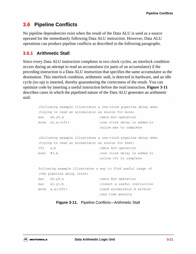
Pipeline Conflicts
3.6 Pipeline Conflicts
No pipeline dependencies exist when the result of the Data ALU is used as a source operand for the immediately following Data ALU instruction. However, Data ALU operations can produce pipeline conflicts as described in the following paragraphs.
3.6.1 Arithmetic Stall
Since every Data ALU instruction completes in two clock cycles, an interlock condition occurs during an attempt to read an accumulator (or parts of an accumulator) if the preceding instruction is a Data ALU instruction that specifies the same accumulator as the destination. This interlock condition, arithmetic stall, is detected in hardware, and an idle cycle (no op) is inserted, thereby guaranteeing the correctness of the result. You can optimize code by inserting a useful instruction before the read instruction. Figure 3-11 describes cases in which the pipelined nature of the Data ALU generates an arithmetic stall.
Figure 3-11. Pipeline Conflicts—Arithmetic Stall
;following example illustrates a one-clock pipeline delay when
;trying to read an accumulator as source for move:
mac x0,y0,a ;data ALU operation
move a1,x:(r0)+ ;one clock delay is added to
;allow mac to complete
;following example illustrates a one-clock pipeline delay when
;trying to read an accumulator as source for bset:
tfr a,b ;data ALU operation
bset #3,b ;one clock delay is added to
;allow tfr to complete
following example illustrates a way to find useful usage of
;the pipeline delay clock:
mac x0,y0,a ;data ALU operation
mac x1,y1,b ;insert a useful instruction
move a,x:(r0)+ ;read accumulator A without
;any time penalty
Data Arithmetic Logic Unit 3-21
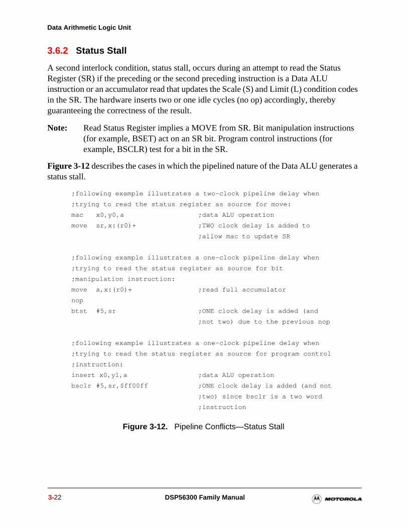
Data Arithmetic Logic Unit
3.6.2 Status Stall
A second interlock condition, status stall, occurs during an attempt to read the Status Register (SR) if the preceding or the second preceding instruction is a Data ALU instruction or an accumulator read that updates the Scale (S) and Limit (L) condition codes in the SR. The hardware inserts two or one idle cycles (no op) accordingly, thereby guaranteeing the correctness of the result.
Note: Read Status Register implies a MOVE from SR. Bit manipulation instructions (for example, BSET) act on an SR bit. Program control instructions (for example, BSCLR) test for a bit in the SR.
Figure 3-12 describes the cases in which the pipelined nature of the Data ALU generates a status stall.
Figure 3-12. Pipeline Conflicts—Status Stall
;following example illustrates a two-clock pipeline delay when
;trying to read the status register as source for move:
mac x0,y0,a ;data ALU operation
move sr,x:(r0)+ ;TWO clock delay is added to
;allow mac to update SR
;following example illustrates a one-clock pipeline delay when
;trying to read the status register as source for bit
;manipulation instruction:
move a,x:(r0)+ ;read full accumulator
nop
btst #5,sr ;ONE clock delay is added (and
;not two) due to the previous nop
;following example illustrates a one-clock pipeline delay when
;trying to read the status register as source for program control
;instruction:
insert x0,y1,a ;data ALU operation
bsclr #5,sr,$ff00ff ;ONE clock delay is added (and not
;two) since bsclr is a two word
;instruction
3-22 DSP56300 Family Manual
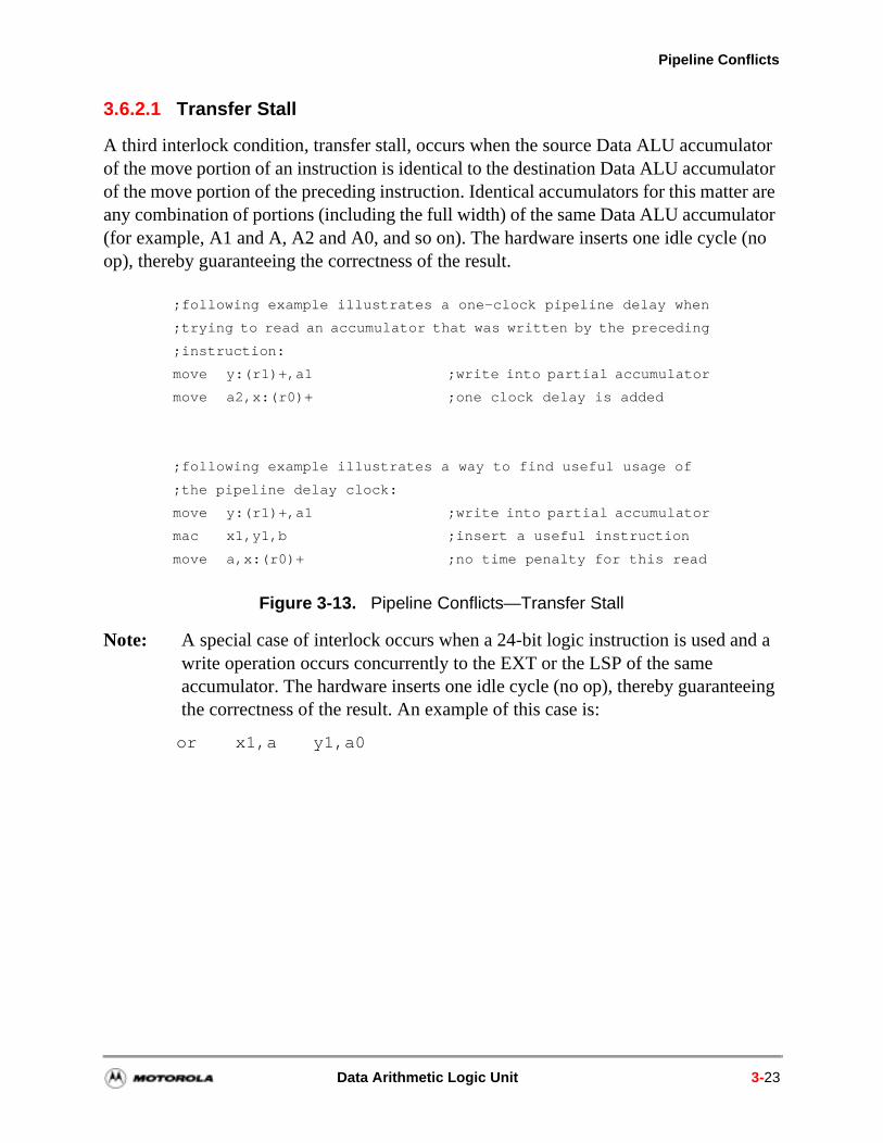
Pipeline Conflicts
3.6.2.1 Transfer Stall
A third interlock condition, transfer stall, occurs when the source Data ALU accumulator of the move portion of an instruction is identical to the destination Data ALU accumulator of the move portion of the preceding instruction. Identical accumulators for this matter are any combination of portions (including the full width) of the same Data ALU accumulator (for example, A1 and A, A2 and A0, and so on). The hardware inserts one idle cycle (no op), thereby guaranteeing the correctness of the result.
Note: A special case of interlock occurs when a 24-bit logic instruction is used and a write operation occurs concurrently to the EXT or the LSP of the same accumulator. The hardware inserts one idle cycle (no op), thereby guaranteeing the correctness of the result. An example of this case is:
or x1,a y1,a0
Figure 3-13. Pipeline Conflicts—Transfer Stall
;following example illustrates a one-clock pipeline delay when
;trying to read an accumulator that was written by the preceding
;instruction:
move y:(r1)+,a1 ;write into partial accumulator
move a2,x:(r0)+ ;one clock delay is added
;following example illustrates a way to find useful usage of
;the pipeline delay clock:
move y:(r1)+,a1 ;write into partial accumulator
mac x1,y1,b ;insert a useful instruction
move a,x:(r0)+ ;no time penalty for this read
Data Arithmetic Logic Unit 3-23

Data Arithmetic Logic Unit
3-24 DSP56300 Family Manual
er:
r to a
e ) to
Chapter 4Address Generation UnitThe Address Generation Unit (AGU) is one of three execution units on the DSP56300 core. The AGU performs the effective address calculations (using integer arithmetic) necessary to address data operands in memory and contains the registers used to generate the addresses. To minimize address-generation overhead, the AGU operates in parallel with other chip resources. It implements four types of arithmetic:
Linear
Modulo
Multiple wrap-around modulo
Reverse-carry
4.1 AGU Architecture
The AGU is divided into halves, each with its own Address Arithmetic Logic Unit (Address ALU). Each Address ALU has four sets of register triplets, and each register triplet is composed of an address register, an offset register, and a modifier register. The two Address ALUs are identical. Each contains a 24-bit full adder—an offset adder—which can perform the following additions/subtractions on an address regist
Plus one
Minus one
Plus the contents of the respective offset register N
Minus the contents of the respective offset register N
A second full adder—a modulo adder—adds the summed result of the first full addemodulo value, M or minus M, where M is stored in the respective modifier register. Athird full adder—a reverse-carry adder—can perform the following additions, with thcarry propagating in the reverse direction (that is, from the Most Significant Bit (MSBthe Least Significant Bit (LSB):
Plus one
Minus one
DSP56300 Family Manual 4-1
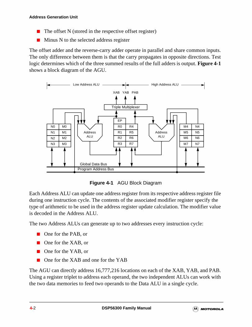
Address Generation Unit
The offset N (stored in the respective offset register)
Minus N to the selected address register
The offset adder and the reverse-carry adder operate in parallel and share common inputs. The only difference between them is that the carry propagates in opposite directions. Test logic determines which of the three summed results of the full adders is output. Figure 4-1 shows a block diagram of the AGU.
Each Address ALU can update one address register from its respective address register file during one instruction cycle. The contents of the associated modifier register specify the type of arithmetic to be used in the address register update calculation. The modifier value is decoded in the Address ALU.
The two Address ALUs can generate up to two addresses every instruction cycle:
One for the PAB, or
One for the XAB, or
One for the YAB, or
One for the XAB and one for the YAB
The AGU can directly address 16,777,216 locations on each of the XAB, YAB, and PAB. Using a register triplet to address each operand, the two independent ALUs can work with the two data memories to feed two operands to the Data ALU in a single cycle.
Figure 4-1 AGU Block Diagram
N0
N1
N2
N3 M3
M2
M1
M0
AddressALU
AddressALU
R0
R1
R2
R3 R7
R6
R5
R4 M4
M5
M6
M7 N7
N6
N5
N4
Triple Multiplexer
Low Address ALU High Address ALU
XAB YAB PAB
Program Address Bus
EP
Global Data Bus
4-2 DSP56300 Family Manual
AGU Architecture
ess
ister, that gister The
tput nates
The registers are:
Address Registers R[0–3] on the Low Address ALU and R[4–7] on the High Address ALU
Offset Registers N[0–3] on the Low Address ALU and N[4–7] on the High AddrALU
Modifier Registers M[0–3] on the Low Address ALU and M[4–7] on the High Address ALU
These registers are referred to as Rn for any address register, Nn for any offset regand Mn for any modifier register. The Rn, Nn, and Mn registers are register triplets—is, the offset and modulo registers of one triplet can be used only with an address rethat belongs to the same triplet. For example, only N2 and M2 can be used with R2.eight triplets are as follows:
Low Address ALU register triplets
— R0:N0:M0
— R1:N1:M1
— R2:N2:M2
— R3:N3:M3
High Address ALU register triplets
— R4:N4:M4
— R5:N5:M5
— R6:N6:M6
— R7:N7:M7
The Global Data Bus (GDB) can read from or write to each register. The address oumultiplexers select the address for the XAB, YAB, and PAB, where the address origifrom the R[0–3] or R[4–7] registers.
Address Generation Unit 4-3
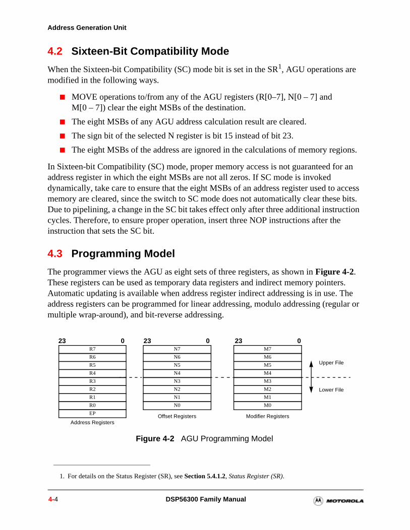
Address Generation Unit
ions.
r an
access e bits. ction
ers. The ular or
4.2 Sixteen-Bit Compatibility Mode
When the Sixteen-bit Compatibility (SC) mode bit is set in the SR1, AGU operations are modified in the following ways.
MOVE operations to/from any of the AGU registers (R[0–7], N[0 – 7] and M[0 – 7]) clear the eight MSBs of the destination.
The eight MSBs of any AGU address calculation result are cleared.
The sign bit of the selected N register is bit 15 instead of bit 23.
The eight MSBs of the address are ignored in the calculations of memory reg
In Sixteen-bit Compatibility (SC) mode, proper memory access is not guaranteed foaddress register in which the eight MSBs are not all zeros. If SC mode is invoked dynamically, take care to ensure that the eight MSBs of an address register used tomemory are cleared, since the switch to SC mode does not automatically clear thesDue to pipelining, a change in the SC bit takes effect only after three additional instrucycles. Therefore, to ensure proper operation, insert three NOP instructions after theinstruction that sets the SC bit.
4.3 Programming Model
The programmer views the AGU as eight sets of three registers, as shown in Figure 4-2. These registers can be used as temporary data registers and indirect memory pointAutomatic updating is available when address register indirect addressing is in use.address registers can be programmed for linear addressing, modulo addressing (regmultiple wrap-around), and bit-reverse addressing.
1. For details on the Status Register (SR), see Section 5.4.1.2, Status Register (SR).
Figure 4-2 AGU Programming Model
R7
R6
R5
R4
R3
R2
R1
R0
N7
N6
N5
N4
N3
N2
N1
N0
Offset Registers Modifier Registers
Upper File
Lower File
Address Registers
M7
M6
M5
M4
M3
M2
M1
M0
EP
23 0 23 0 23 0
4-4 DSP56300 Family Manual
Programming Model
e data. ddress ust be egister
to the (Mn)
nits. s its etic ister in
uring ry, as
k.
the tion to EP JSR, ster ) tack
ent of an
4.3.1 Address Register Files
The eight 24-bit address registers R[0 – 7] can contain addresses or general-purposThe 24-bit address in a selected address register is used in calculating the effective aof an operand. During parallel X and Y data memory moves, the address registers mprogrammed as two separate files, R[0–3] and R[4–7]. The contents of an address rcan point directly to data, or they can be offset.
In addition, an address register (Rn) can be pre-updated or post-updated accordingaddressing mode selected. If an Rn is updated, the corresponding modifier register specifies the type of update arithmetic. Offset registers (Nn) are used for the update-by-offset addressing modes.
The address register modification is performed by one of the two modulo arithmetic uMost addressing modes modify the selected address register in a read-modify-writefashion. The address register is read, the associated modulo arithmetic unit modifiecontents, and the register is written with the appropriate output of the modulo arithmunit. The contents of the offset and modifier registers control the form of address regmodification performed by the modulo arithmetic unit. These registers are discussedSection 4.3.3 and Section 4.3.4.
4.3.2 Stack Extension Pointer
The hardware stack is an area in internal memory that provides temporary storage dprogram execution. The stack exists in either the X data memory or the Y data memoselected by the XYS bit in the Operating Mode Register (OMR) (refer to Chapter 5, Program Control Unit for a detailed description of the OMR). The stack uses push operations to add data to the stack and pull operations to retrieve data from the stac
The contents of the 24-bit stack Extension Pointer (EP) register point to the stack extension whenever the stack extension is enabled and move operations to or from on-chip hardware stack are needed. The EP register points to the next available locawhich a push can be made (that is, it points just past the last item on the stack). Theregister is a read/write register and is referenced implicitly (for example, by the DO, or RTI instructions) or directly (for example, by the MOVEC instruction). The EP regiis not initialized during hardware reset, and must be set (using a MOVEC instructionprior to enabling the stack extension. For more information on the operation of the sextension, see Chapter 5, Program Control Unit.
4.3.3 Offset Register Files
The eight 24-bit offset registers, N[0–7], contain offset values to increment or decremaddress registers in address register update calculations. For example, the contents
Address Generation Unit 4-5
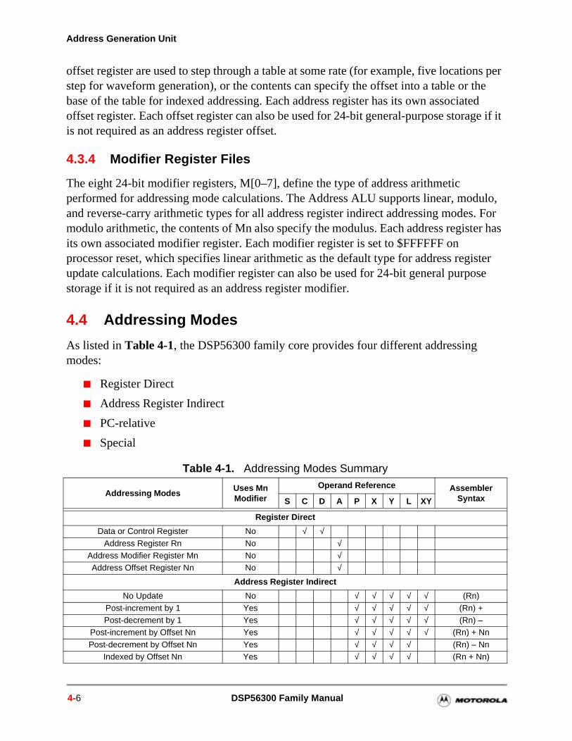
Address Generation Unit
ulo, . For er has
ister ose
offset register are used to step through a table at some rate (for example, five locations per step for waveform generation), or the contents can specify the offset into a table or the base of the table for indexed addressing. Each address register has its own associated offset register. Each offset register can also be used for 24-bit general-purpose storage if it is not required as an address register offset.
4.3.4 Modifier Register Files
The eight 24-bit modifier registers, M[0–7], define the type of address arithmetic performed for addressing mode calculations. The Address ALU supports linear, modand reverse-carry arithmetic types for all address register indirect addressing modesmodulo arithmetic, the contents of Mn also specify the modulus. Each address registits own associated modifier register. Each modifier register is set to $FFFFFF on processor reset, which specifies linear arithmetic as the default type for address regupdate calculations. Each modifier register can also be used for 24-bit general purpstorage if it is not required as an address register modifier.
4.4 Addressing Modes
As listed in Table 4-1, the DSP56300 family core provides four different addressing modes:
Register Direct
Address Register Indirect
PC-relative
Special
Table 4-1. Addressing Modes Summary
Addressing ModesUses Mn Modifier
Operand Reference Assembler SyntaxS C D A P X Y L XY
Register Direct
Data or Control Register No √ √Address Register Rn No √
Address Modifier Register Mn No √Address Offset Register Nn No √
Address Register Indirect
No Update No √ √ √ √ √ (Rn)
Post-increment by 1 Yes √ √ √ √ √ (Rn) +Post-decrement by 1 Yes √ √ √ √ √ (Rn) –
Post-increment by Offset Nn Yes √ √ √ √ √ (Rn) + Nn
Post-decrement by Offset Nn Yes √ √ √ √ (Rn) – NnIndexed by Offset Nn Yes √ √ √ √ (Rn + Nn)
4-6 DSP56300 Family Manual
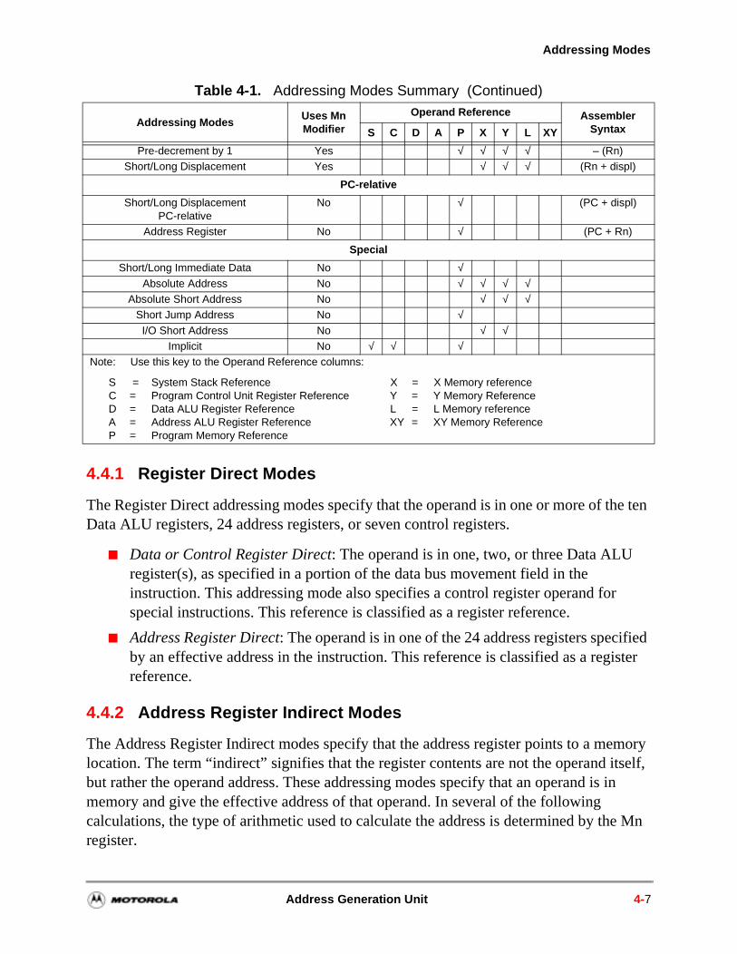
Addressing Modes
tself, in
e Mn
4.4.1 Register Direct Modes
The Register Direct addressing modes specify that the operand is in one or more of the ten Data ALU registers, 24 address registers, or seven control registers.
Data or Control Register Direct: The operand is in one, two, or three Data ALU register(s), as specified in a portion of the data bus movement field in the instruction. This addressing mode also specifies a control register operand for special instructions. This reference is classified as a register reference.
Address Register Direct: The operand is in one of the 24 address registers specified by an effective address in the instruction. This reference is classified as a register reference.
4.4.2 Address Register Indirect Modes
The Address Register Indirect modes specify that the address register points to a memory location. The term “indirect” signifies that the register contents are not the operand ibut rather the operand address. These addressing modes specify that an operand ismemory and give the effective address of that operand. In several of the following calculations, the type of arithmetic used to calculate the address is determined by thregister.
Pre-decrement by 1 Yes √ √ √ √ – (Rn)Short/Long Displacement Yes √ √ √ (Rn + displ)
PC-relative
Short/Long DisplacementPC-relative
No √ (PC + displ)
Address Register No √ (PC + Rn)
Special
Short/Long Immediate Data No √Absolute Address No √ √ √ √
Absolute Short Address No √ √ √Short Jump Address No √
I/O Short Address No √ √Implicit No √ √ √
Note: Use this key to the Operand Reference columns:
S = System Stack Reference X = X Memory referenceC = Program Control Unit Register Reference Y = Y Memory ReferenceD = Data ALU Register Reference L = L Memory referenceA = Address ALU Register Reference XY = XY Memory ReferenceP = Program Memory Reference
Table 4-1. Addressing Modes Summary (Continued)
Addressing ModesUses Mn Modifier
Operand Reference Assembler SyntaxS C D A P X Y L XY
Address Generation Unit 4-7
Address Generation Unit
of
. same
r. same
of the egister
of the egister
ts e
ess d ter is
the
No Update (Rn)—The operand address is in the address register. The contentsthe address register are unchanged by executing the instruction.
Example: MOVE x:(Rn),x0
Post-Increment By One (Rn) + —The operand address is in the address registerAfter the operand address is used, it is incremented by one and stored in the address register. The Nn register is ignored.
Example: MOVE x:(Rn)+,x0
Post-Decrement By One (Rn) – —The operand address is in the address registeAfter the operand address is used, it is decremented by one and stored in theaddress register. The Nn register is ignored.
Example: MOVE x:(Rn)-,x0
Post-Increment By Offset Nn (Rn) + Nn—The operand address is in the address register. After the operand address is used, it is incremented by the contents Nn register and stored in the same address register. The contents of the Nn rare unchanged.
Example: MOVE x:(Rn)+Nn,x0
Post-Decrement By Offset Nn (Rn) – Nn—The operand address is in the addressregister. After the operand address is used, it is decremented by the contentsNn register and stored in the same address register. The contents of the Nn rare unchanged.
Example: MOVE x:(Rn)-Nn,x0
Indexed By Offset Nn (Rn + Nn)—The operand address is the sum of the contenof the address register and the contents of the address offset register, Nn. Thcontents of the Rn and Nn registers are unchanged.
Example: MOVE x:(Rn+Nn),x0
Pre-Decrement By One -(Rn)—The operand address is the contents of the addrregister decremented by one. The contents of Rn are decremented by one anstored in the same address register before the memory access. The Nn regisignored.
Example: MOVE x:-(Rn),x0
Short Displacement (Rn + Short Displacement)—The operand address is the sumof the contents of the address register Rn and a short signed displacement occupying seven bits in the instruction word. The displacement is first sign-extended to 24 bits (16 bits in SC mode) and then added to Rn to obtain
4-8 DSP56300 Family Manual
Addressing Modes
he ddress d as a
and
he nd
C and
of ntents
of the
DI, REP
operand address. The contents of the Rn register are unchanged. The Nn register is ignored. This reference is classified as a memory reference.
Example: MOVE x:(Rn+63),x0
Long Displacement (Rn + Long Displacement)—This addressing mode requires one word (label) of instruction extension. The operand address is the sum of tcontents of the address register and the extension word. The contents of the aregister are unchanged. The Nn register is ignored. This reference is classifiememory reference.
Example: MOVE x:(Rn+64),x0
4.4.3 PC-Relative Modes
In the PC-relative addressing modes, the operand address is obtained by adding a displacement, represented in two’s-complement format, to the value of the ProgramCounter (PC). The PC points to the address of the instruction opcode word. The NnMn registers are ignored, and the arithmetic used is always linear.
Short Displacement PC-Relative—The short displacement occupies nine bits in tinstruction operation word. The displacement is first sign-extended to 24 bits athen added to the PC to obtain the operand address.
Long Displacement PC-Relative—This addressing mode requires one word of instruction extension. The operand address is the sum of the contents of the Pthe extension word.
Address Register PC-Relative—The operand address is the sum of the contentsthe PC and the address register. The Mn and Nn registers are ignored. The coof the address register are unchanged.
4.4.4 Special Address Modes
The special address modes do not use an address register in specifying an effectiveaddress. These modes either specify the operand or the operand address in a field instruction, or they implicitly reference an operand.
Immediate Data—This addressing mode requires one word of instruction extension. The immediate data is a word operand in the extension word of theinstruction. This reference is classified as a program reference.
Immediate Short Data—The 8-bit or 12-bit operand is part of the instruction operation word. An 8-bit operand is used for an immediate move to register, ANand ORI instructions. It is zero-extended. A 12-bit operand is used for DO and
Address Generation Unit 4-9
Address Generation Unit
n ory
a
d with
ee
d .
st-In, ourier rs) er
ddress can be able:
instructions. It is also zero-extended. This reference is classified as a program reference.
Absolute Address—This addressing mode requires one word of instruction extension. The operand address is in the extension word. This reference is classified as a memory reference and a program reference.
Absolute Short Address—The operand address occupies six bits in the instructiooperation word, and it is zero-extended. This reference is classified as a memreference.
Short Jump Address—The operand occupies 12 bits in the instruction operationword. The address is zero-extended to 24 bits. This reference is classified as program reference.
I/O Short Address—The operand address occupies 6 bits in the instruction operation word, and it is one-extended. The I/O short addressing mode is usethe bit manipulation and move peripheral data instructions.
Implicit Reference—Some instructions make implicit reference to the Program Counter (PC), System Stack (SSH, SSL), Loop Address (LA) register, Loop Counter (LC), or Status Register (SR). These registers are implied by the instruction, and their use is defined by the individual instruction descriptions. SChapter 12, Guide to the Instruction Set, for more information.
4.5 Address Modifier Types
The DSP56300 family core Address ALU supports linear, reverse-carry, modulo, anmultiple wrap-around modulo arithmetic types for all address register indirect modesThese arithmetic types easily allow the creation of data structures in memory for FirFirst-Out (FIFO) queues, delay lines, circular buffers, stacks, and bit-reversed Fast FTransform (FFT) buffers. Data is manipulated by updating address registers (pointerather than moving large blocks of data. The contents of the address modifier registdefine the type of arithmetic to be performed for addressing mode calculations. For modulo arithmetic, the address modifier register also specifies the modulus. Each aregister has its own associated modifier register. All address register indirect modes used with any address modifier type. The following address modifier types are avail
Linear addressing—Useful for general-purpose addressing
Reverse-carry addressing—Useful for 2k-point FFT addressing
4-10 DSP56300 Family Manual
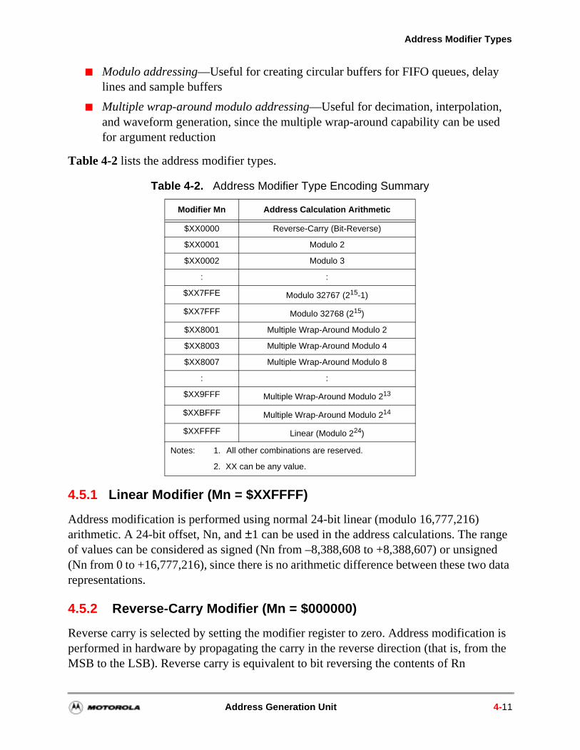
Address Modifier Types
sed
ge ned data
on is the
Modulo addressing—Useful for creating circular buffers for FIFO queues, delaylines and sample buffers
Multiple wrap-around modulo addressing—Useful for decimation, interpolation, and waveform generation, since the multiple wrap-around capability can be ufor argument reduction
Table 4-2 lists the address modifier types. .
4.5.1 Linear Modifier (Mn = $XXFFFF)
Address modification is performed using normal 24-bit linear (modulo 16,777,216) arithmetic. A 24-bit offset, Nn, and ±1 can be used in the address calculations. The ranof values can be considered as signed (Nn from –8,388,608 to +8,388,607) or unsig(Nn from 0 to +16,777,216), since there is no arithmetic difference between these tworepresentations.
4.5.2 Reverse-Carry Modifier (Mn = $000000)
Reverse carry is selected by setting the modifier register to zero. Address modificatiperformed in hardware by propagating the carry in the reverse direction (that is, fromMSB to the LSB). Reverse carry is equivalent to bit reversing the contents of Rn
Table 4-2. Address Modifier Type Encoding Summary
Modifier Mn Address Calculation Arithmetic
$XX0000 Reverse-Carry (Bit-Reverse)
$XX0001 Modulo 2
$XX0002 Modulo 3
: :
$XX7FFE Modulo 32767 (215-1)
$XX7FFF Modulo 32768 (215)
$XX8001 Multiple Wrap-Around Modulo 2
$XX8003 Multiple Wrap-Around Modulo 4
$XX8007 Multiple Wrap-Around Modulo 8
: :
$XX9FFF Multiple Wrap-Around Modulo 213
$XXBFFF Multiple Wrap-Around Modulo 214
$XXFFFF Linear (Modulo 224)
Notes: 1. All other combinations are reserved.
2. XX can be any value.
Address Generation Unit 4-11
Address Generation Unit
ress)
ks,
on the dress the
ntents e, fer ). ng
raps
ust be
n) + a new ps
(redefining the MSB as the LSB, the next MSB as bit 1, and so on) and the offset value, Nn, adding normally, and then bit reversing the result. If the +Nn addressing mode is used with this address modifier and Nn contains a value 2(k – 1) (a power of two), this addressing modifier is equivalent to bit reversing the k LSBs of Rn, incrementing Rn by one, and bit reversing the k LSBs of Rn again. This address modification is useful for addressing the two middle factors in 2k-point FFT addressing and unscrambling 2k-point FFT data. The range of values for Nn is 0 to + 8 M (that is, Nn = 223), which allows bit-reverse addressing for FFTs up to 16,777,216 points.
4.5.3 Modulo Modifier (Mn = Modulus – 1)
Address modification is performed using modulo M, where M ranges from 2 to +32,768. Modulo M arithmetic causes the address register value to remain within an address range of size M, defined by a lower and upper address boundary.
The value m = M – 1 is stored in the modifier register. The lower boundary (base addvalue must have zeros in the k LSBs, where 2k ≥ M, and therefore must be a multiple of 2k. The upper boundary is the lower boundary plus the modulo size minus one (baseaddress + M – 1). Since M ≤ 2k, once M is chosen, a sequential series of memory bloceach of length 2k, is created where these circular buffers can be located. If M < 2k, there is a space between sequential circular buffers of (2k) – M.
The address pointer is not required to start at the lower address boundary or to endupper address boundary; it can initially point anywhere within the defined modulo adrange. Neither the lower nor the upper boundary of the modulo region is stored; onlysize of the modulo region is stored in Mn. The boundaries are determined by the coof Rn. Assuming the Address Register Indirect with post-increment addressing mod(Rn)+, if the address register pointer increments past the upper boundary of the buf(base address + M – 1), it wraps around through the base address (lower boundaryAlternatively, assuming the Address Register Indirect with post-decrement addressimode, (Rn)-, if the address decrements past the lower boundary (base address), it waround through the base address + M – 1 (upper boundary).
If an offset, Nn, is used in the address calculations, the 24-bit absolute value, |Nn|, mless than or equal to M for proper modulo addressing. If Nn > M, the result is data dependent and unpredictable, except for the special case where Nn = P × 2k, a multiple of the block size where P is a positive integer. For this special case, when using the (RNn addressing mode, the pointer, Rn, jumps linearly to the same relative address inbuffer, which is P blocks forward in memory. Similarly, for (Rn) – Nn, the pointer jumP blocks backward in memory.
4-12 DSP56300 Family Manual
Address Modifier Types
tic pe of es, d
,
n an M – 1 to e zeros
begin
he
dress + than d for occur
This technique is useful in sequentially processing multiple tables or N-dimensional arrays. The range of values for Nn is –8,388,608 to +8,388,607. The modulo arithmeunit automatically wraps around the address pointer by the required amount. This tyaddress modification is useful for creating circular buffers for FIFO queues, delay linand sample buffers up to 8,388,607 words long, and for decimation, interpolation, anwaveform generation. The special case of (Rn) ± Nn modulo M with Nn = P × 2k is useful for performing the same algorithm on multiple blocks of data in memory, for examplewhen performing parallel Infinite Impulse Response (IIR) filtering.
4.5.4 Multiple Wrap-Around Modulo Modifier
The Multiple Wrap-Around Addressing mode is selected by setting bit 15 of the Mn register to one and clearing bit 14 to zero, as shown in Table 4-2 on page 4-11. The address modification is performed using modulo M, where M is a power of 2 in the rangefrom 21 to 214. Modulo M arithmetic causes the address register value to remain withiaddress range of size M defined by a lower and upper address boundary. The valueis stored in the Mn register’s 14 Least Significant Bits (bits 13–0), while bit 15 is set one and bit 14 is cleared to zero. The lower boundary (base address) value must havin the k LSBs, where 2k = M, and therefore must be a multiple of 2k. The upper boundary is the lower boundary plus the modulo size minus one (base address + M – 1).
The address pointer is not required to start at the lower address boundary and may anywhere within the defined modulo address range (between the lower and upper boundaries). If the address register pointer increments past the upper boundary of tbuffer (base address + M – 1), it wraps around to the base address. If the address decrements past the lower boundary (base address), it wraps around to the base adM – 1. If an offset Nn is used in the address calculations, it is not required to be lessor equal to M for proper modulo addressing, since multiple wrap around is supporte(Rn) + Nn, (Rn) – Nn, and (Rn + Nn) address updates. Multiple wrap around cannot with (Rn)+, (Rn)–, and –(Rn) addressing modes.
Address Generation Unit 4-13

Address Generation Unit
4-14 DSP56300 Family Manual
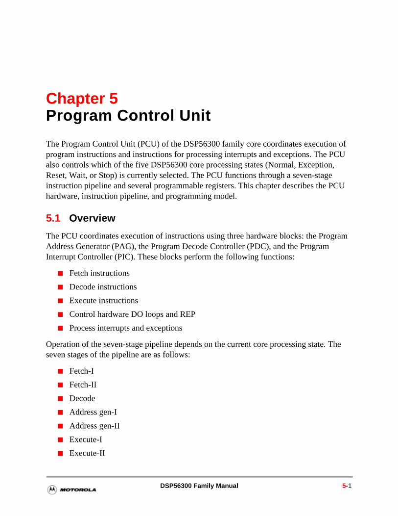
Chapter 5Program Control Unit
The Program Control Unit (PCU) of the DSP56300 family core coordinates execution of program instructions and instructions for processing interrupts and exceptions. The PCU also controls which of the five DSP56300 core processing states (Normal, Exception, Reset, Wait, or Stop) is currently selected. The PCU functions through a seven-stage instruction pipeline and several programmable registers. This chapter describes the PCU hardware, instruction pipeline, and programming model.
5.1 Overview
The PCU coordinates execution of instructions using three hardware blocks: the Program Address Generator (PAG), the Program Decode Controller (PDC), and the Program Interrupt Controller (PIC). These blocks perform the following functions:
Fetch instructions
Decode instructions
Execute instructions
Control hardware DO loops and REP
Process interrupts and exceptions
Operation of the seven-stage pipeline depends on the current core processing state. The seven stages of the pipeline are as follows:
Fetch-I
Fetch-II
Decode
Address gen-I
Address gen-II
Execute-I
Execute-II
DSP56300 Family Manual 5-1
Program Control Unit
ack, his
To preserve current operation and status values while processing exceptions and interrupts, the PCU provides a System Stack to store current register contents before executing the exception/interrupt handler program. These contents are restored when control returns to the current program. In addition to these standard program flow-control resources, the PCU provides special support for hardware DO loops and an instruction REPEAT mechanism.
To perform its functions, the PCU uses a number of programmable registers. The organization of these registers forms the programming model for the PCU:
General configuration and status:
— Operating Mode Register (OMR)—24-bit, read/write
— Status Register (SR)—24-bit, read/write
System Stack configuration and operation:
— System Stack (SS) register file—hardware stack, 48-bit × 16 locations, read/write
— System Stack High (SSH) Register—24-bit, read/write
— System Stack Low (SSL) Register—24-bit, read/write
— Stack Pointer (SP) Register—24-bit, read/write
— Stack Counter (SC) Register—5-bit, read/write
— Stack Size (SZ) Register—24-bit, read/write
Note: The stack Extension Pointer (EP) Register is also used with the System Stbut is physically part of the Address Generation Unit. For a description of tregister, refer to Chapter 4, Address Generation Unit.
Program/Loop/Exception processing control:
— Program Counter (PC) Register—24-bit, read/write
— Loop Address (LA) Register—24-bit, read/write
— Loop Counter (LC) Register—24-bit, read/write
— Vector Base Address (VBA) Register—24-bit, read/write
5-2 DSP56300 Family Manual
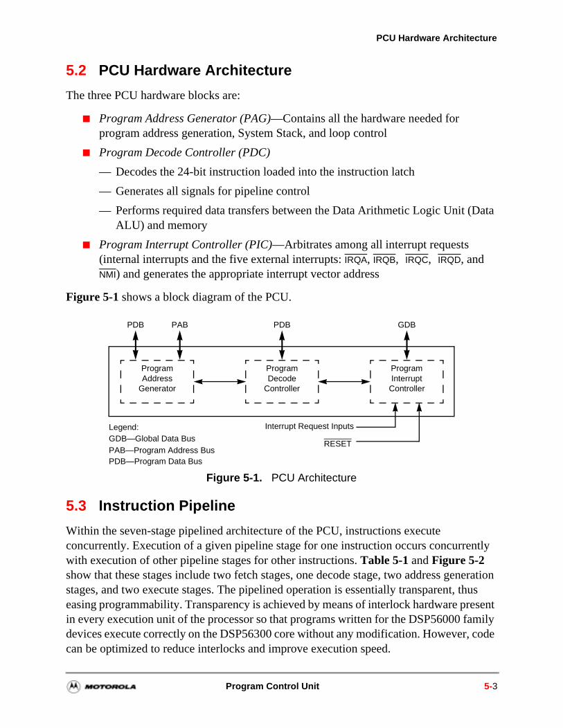
PCU Hardware Architecture
ata
ntly
neration thus resent amily code
5.2 PCU Hardware Architecture
The three PCU hardware blocks are:
Program Address Generator (PAG)—Contains all the hardware needed for program address generation, System Stack, and loop control
Program Decode Controller (PDC)
— Decodes the 24-bit instruction loaded into the instruction latch
— Generates all signals for pipeline control
— Performs required data transfers between the Data Arithmetic Logic Unit (DALU) and memory
Program Interrupt Controller (PIC)—Arbitrates among all interrupt requests (internal interrupts and the five external interrupts: IRQA, IRQB, IRQC, IRQD, and NMI) and generates the appropriate interrupt vector address
Figure 5-1 shows a block diagram of the PCU.
5.3 Instruction Pipeline
Within the seven-stage pipelined architecture of the PCU, instructions execute concurrently. Execution of a given pipeline stage for one instruction occurs concurrewith execution of other pipeline stages for other instructions. Table 5-1 and Figure 5-2 show that these stages include two fetch stages, one decode stage, two address gestages, and two execute stages. The pipelined operation is essentially transparent, easing programmability. Transparency is achieved by means of interlock hardware pin every execution unit of the processor so that programs written for the DSP56000 fdevices execute correctly on the DSP56300 core without any modification. However,can be optimized to reduce interlocks and improve execution speed.
Figure 5-1. PCU Architecture
ProgramInterrupt
Controller
ProgramDecode
Controller
ProgramAddress
Generator
PDB PAB PDB GDB
Interrupt Request InputsLegend:GDB—Global Data Bus
PDB—Program Data BusPAB—Program Address Bus
RESET
Program Control Unit 5-3
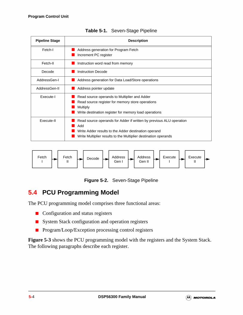
Program Control Unit
5.4 PCU Programming Model
The PCU programming model comprises three functional areas:
Configuration and status registers
System Stack configuration and operation registers
Program/Loop/Exception processing control registers
Figure 5-3 shows the PCU programming model with the registers and the System Stack. The following paragraphs describe each register.
Table 5-1. Seven-Stage Pipeline
Pipeline Stage Description
Fetch-I Address generation for Program Fetch Increment PC register
Fetch-II Instruction word read from memory
Decode Instruction Decode
AddressGen-I Address generation for Data Load/Store operations
AddressGen-II Address pointer update
Execute-I Read source operands to Multiplier and Adder
Read source register for memory store operations Multiply Write destination register for memory load operations
Execute-II Read source operands for Adder if written by previous ALU operation
Add Write Adder results to the Adder destination operand Write Multiplier results to the Multiplier destination operands
Figure 5-2. Seven-Stage Pipeline
FetchI
FetchII
Decode Address Gen I
AddressGen II
ExecuteI
ExecuteII
5-4 DSP56300 Family Manual
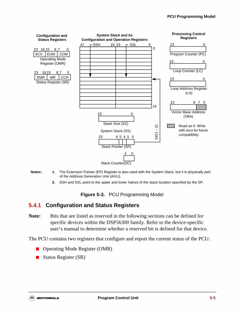
PCU Programming Model
e.
CU:
5.4.1 Configuration and Status Registers
Note: Bits that are listed as reserved in the following sections can be defined for specific devices within the DSP56300 family. Refer to the device-specific user’s manual to determine whether a reserved bit is defined for that devic
The PCU contains two registers that configure and report the current status of the P
Operating Mode Register (OMR)
Status Register (SR)
Figure 5-3. PCU Programming Model
SP[3
– 0
]
0
Status Register (SR)
Loop Address Register (LA)
Loop Counter (LC)
Stack Pointer (SP)
Read as 0. Write with zero for future compatibility.
15
System Stack (SS)
Operating Mode Register (OMR)
Vector Base Address (VBA)
Stack Size (SZ)
Stack Counter(SC)
04
23 0
23 0
23 0
47 24 23 0SSH SSL
23 6 5 4 3 0
23 0
8 7
EMR CCR
23 0
23 08 7
16 15 78
1615MR
SCS EOM COM Program Counter (PC)
23 0
Configuration and Status Registers
System Stack and its Processing ControlRegisters
Notes: 1. The Extension Pointer (EP) Register is also used with the System Stack, but it is physically part of the Address Generation Unit (AGU).
2. SSH and SSL point to the upper and lower halves of the stack location specified by the SP.
Configuration and Operation Registers
Program Control Unit 5-5
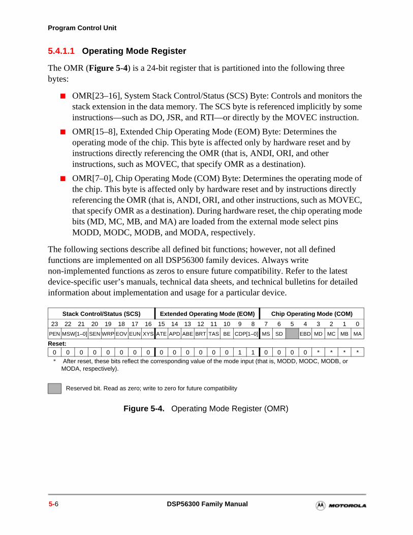
Program Control Unit
the ome n.
y
e of tly
EC, mode
st ailed
5.4.1.1 Operating Mode Register
The OMR (Figure 5-4) is a 24-bit register that is partitioned into the following three bytes:
OMR[23–16], System Stack Control/Status (SCS) Byte: Controls and monitorsstack extension in the data memory. The SCS byte is referenced implicitly by sinstructions—such as DO, JSR, and RTI—or directly by the MOVEC instructio
OMR[15–8], Extended Chip Operating Mode (EOM) Byte: Determines the operating mode of the chip. This byte is affected only by hardware reset and binstructions directly referencing the OMR (that is, ANDI, ORI, and other instructions, such as MOVEC, that specify OMR as a destination).
OMR[7–0], Chip Operating Mode (COM) Byte: Determines the operating modthe chip. This byte is affected only by hardware reset and by instructions direcreferencing the OMR (that is, ANDI, ORI, and other instructions, such as MOVthat specify OMR as a destination). During hardware reset, the chip operating bits (MD, MC, MB, and MA) are loaded from the external mode select pins MODD, MODC, MODB, and MODA, respectively.
The following sections describe all defined bit functions; however, not all defined functions are implemented on all DSP56300 family devices. Always write non-implemented functions as zeros to ensure future compatibility. Refer to the latedevice-specific user’s manuals, technical data sheets, and technical bulletins for detinformation about implementation and usage for a particular device.
Figure 5-4. Operating Mode Register (OMR)
Stack Control/Status (SCS) Extended Operating Mode (EOM) Chip Operating Mode (COM)
23 22 21 20 19 18 17 16 15 14 13 12 11 10 9 8 7 6 5 4 3 2 1 0
PEN MSW[1–0] SEN WRP EOV EUN XYS ATE APD ABE BRT TAS BE CDP[1–0] MS SD EBD MD MC MB MA
Reset:0 0 0 0 0 0 0 0 0 0 0 0 0 0 1 1 0 0 0 0 * * * ** After reset, these bits reflect the corresponding value of the mode input (that is, MODD, MODC, MODB, or
MODA, respectively).
Reserved bit. Read as zero; write to zero for future compatibility
5-6 DSP56300 Family Manual
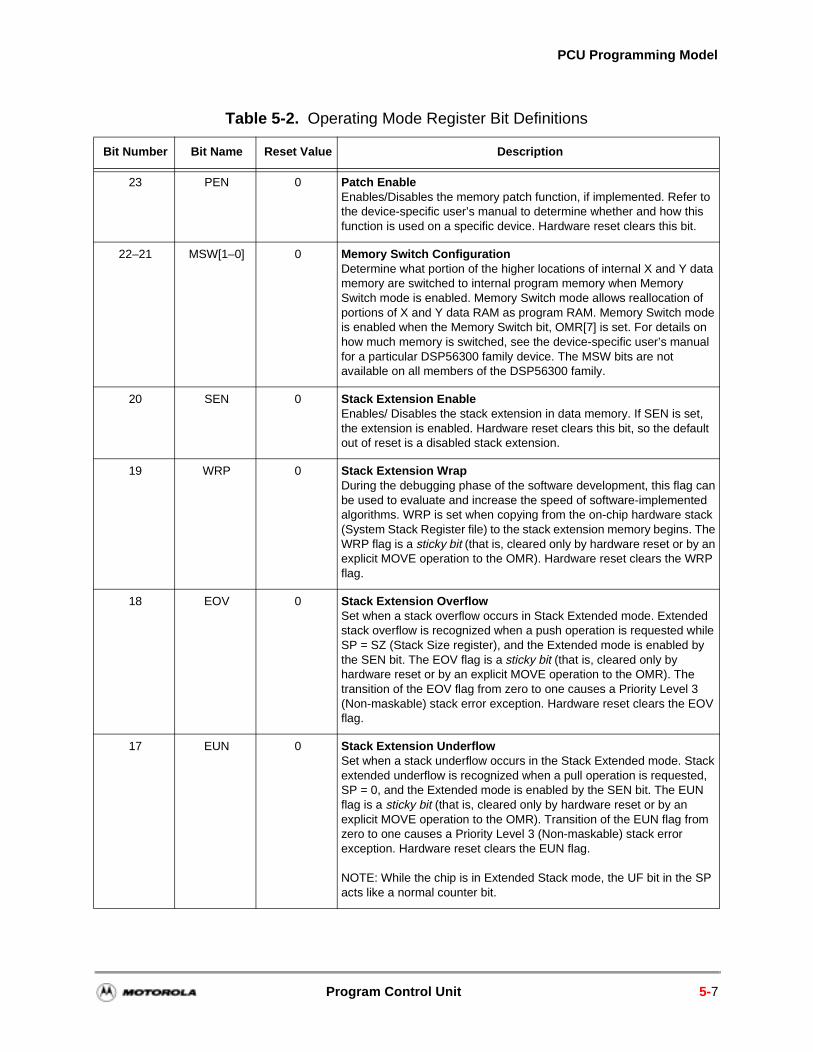
PCU Programming Model
Table 5-2. Operating Mode Register Bit Definitions
Bit Number Bit Name Reset Value Description
23 PEN 0 Patch EnableEnables/Disables the memory patch function, if implemented. Refer to the device-specific user’s manual to determine whether and how this function is used on a specific device. Hardware reset clears this bit.
22–21 MSW[1–0] 0 Memory Switch ConfigurationDetermine what portion of the higher locations of internal X and Y data memory are switched to internal program memory when Memory Switch mode is enabled. Memory Switch mode allows reallocation of portions of X and Y data RAM as program RAM. Memory Switch mode is enabled when the Memory Switch bit, OMR[7] is set. For details on how much memory is switched, see the device-specific user’s manual for a particular DSP56300 family device. The MSW bits are not available on all members of the DSP56300 family.
20 SEN 0 Stack Extension EnableEnables/ Disables the stack extension in data memory. If SEN is set, the extension is enabled. Hardware reset clears this bit, so the default out of reset is a disabled stack extension.
19 WRP 0 Stack Extension WrapDuring the debugging phase of the software development, this flag can be used to evaluate and increase the speed of software-implemented algorithms. WRP is set when copying from the on-chip hardware stack (System Stack Register file) to the stack extension memory begins. The WRP flag is a sticky bit (that is, cleared only by hardware reset or by an explicit MOVE operation to the OMR). Hardware reset clears the WRP flag.
18 EOV 0 Stack Extension OverflowSet when a stack overflow occurs in Stack Extended mode. Extended stack overflow is recognized when a push operation is requested while SP = SZ (Stack Size register), and the Extended mode is enabled by the SEN bit. The EOV flag is a sticky bit (that is, cleared only by hardware reset or by an explicit MOVE operation to the OMR). The transition of the EOV flag from zero to one causes a Priority Level 3 (Non-maskable) stack error exception. Hardware reset clears the EOV flag.
17 EUN 0 Stack Extension UnderflowSet when a stack underflow occurs in the Stack Extended mode. Stack extended underflow is recognized when a pull operation is requested, SP = 0, and the Extended mode is enabled by the SEN bit. The EUN flag is a sticky bit (that is, cleared only by hardware reset or by an explicit MOVE operation to the OMR). Transition of the EUN flag from zero to one causes a Priority Level 3 (Non-maskable) stack error exception. Hardware reset clears the EUN flag.
NOTE: While the chip is in Extended Stack mode, the UF bit in the SP acts like a normal counter bit.
Program Control Unit 5-7
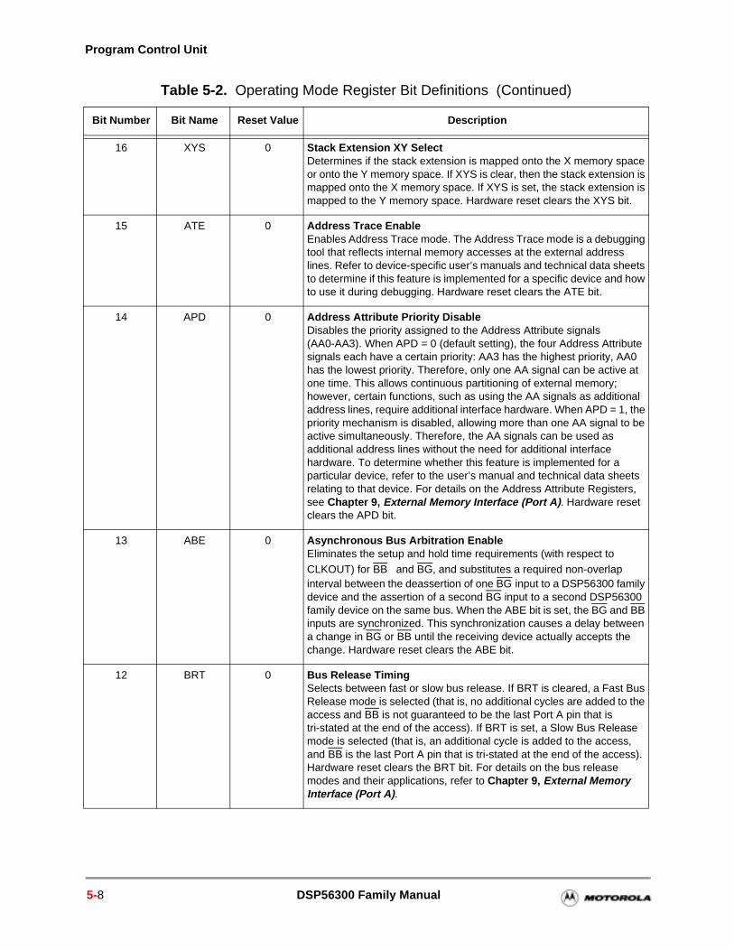
Program Control Unit
16 XYS 0 Stack Extension XY SelectDetermines if the stack extension is mapped onto the X memory space or onto the Y memory space. If XYS is clear, then the stack extension is mapped onto the X memory space. If XYS is set, the stack extension is mapped to the Y memory space. Hardware reset clears the XYS bit.
15 ATE 0 Address Trace EnableEnables Address Trace mode. The Address Trace mode is a debugging tool that reflects internal memory accesses at the external address lines. Refer to device-specific user’s manuals and technical data sheets to determine if this feature is implemented for a specific device and how to use it during debugging. Hardware reset clears the ATE bit.
14 APD 0 Address Attribute Priority DisableDisables the priority assigned to the Address Attribute signals (AA0-AA3). When APD = 0 (default setting), the four Address Attribute signals each have a certain priority: AA3 has the highest priority, AA0 has the lowest priority. Therefore, only one AA signal can be active at one time. This allows continuous partitioning of external memory; however, certain functions, such as using the AA signals as additional address lines, require additional interface hardware. When APD = 1, the priority mechanism is disabled, allowing more than one AA signal to be active simultaneously. Therefore, the AA signals can be used as additional address lines without the need for additional interface hardware. To determine whether this feature is implemented for a particular device, refer to the user’s manual and technical data sheets relating to that device. For details on the Address Attribute Registers, see Chapter 9, External Memory Interface (Port A). Hardware reset clears the APD bit.
13 ABE 0 Asynchronous Bus Arbitration EnableEliminates the setup and hold time requirements (with respect to CLKOUT) for BB and BG, and substitutes a required non-overlap interval between the deassertion of one BG input to a DSP56300 family device and the assertion of a second BG input to a second DSP56300 family device on the same bus. When the ABE bit is set, the BG and BB inputs are synchronized. This synchronization causes a delay between a change in BG or BB until the receiving device actually accepts the change. Hardware reset clears the ABE bit.
12 BRT 0 Bus Release TimingSelects between fast or slow bus release. If BRT is cleared, a Fast Bus Release mode is selected (that is, no additional cycles are added to the access and BB is not guaranteed to be the last Port A pin that is tri-stated at the end of the access). If BRT is set, a Slow Bus Release mode is selected (that is, an additional cycle is added to the access, and BB is the last Port A pin that is tri-stated at the end of the access). Hardware reset clears the BRT bit. For details on the bus release modes and their applications, refer to Chapter 9, External Memory Interface (Port A).
Table 5-2. Operating Mode Register Bit Definitions (Continued)
Bit Number Bit Name Reset Value Description
5-8 DSP56300 Family Manual
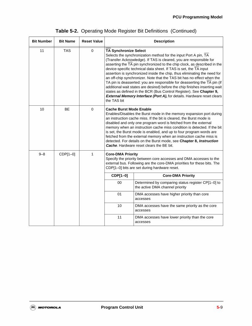
PCU Programming Model
11 TAS 0 TA Synchronize SelectSelects the synchronization method for the input Port A pin, TA (Transfer Acknowledge). If TAS is cleared, you are responsible for asserting the TA pin synchronized to the chip clock, as described in the device-specific technical data sheet. If TAS is set, the TA input assertion is synchronized inside the chip, thus eliminating the need for an off-chip synchronizer. Note that the TAS bit has no effect when the TA pin is deasserted: you are responsible for deasserting the TA pin (if additional wait states are desired) before the chip finishes inserting wait states as defined in the BCR (Bus Control Register). See Chapter 9, External Memory Interface (Port A), for details. Hardware reset clears the TAS bit
10 BE 0 Cache Burst Mode EnableEnables/Disables the Burst mode in the memory expansion port during an instruction cache miss. If the bit is cleared, the Burst mode is disabled and only one program word is fetched from the external memory when an instruction cache miss condition is detected. If the bit is set, the Burst mode is enabled, and up to four program words are fetched from the external memory when an instruction cache miss is detected. For details on the Burst mode, see Chapter 8, Instruction Cache. Hardware reset clears the BE bit.
9–8 CDP[1–0] 1 Core-DMA PrioritySpecify the priority between core accesses and DMA accesses to the external bus. Following are the core-DMA priorities for these bits. The CDP[1–0] bits are set during hardware reset.
CDP[1–0] Core-DMA Priority
00 Determined by comparing status register CP[1–0] to the active DMA channel priority
01 DMA accesses have higher priority than core accesses
10 DMA accesses have the same priority as the core accesses
11 DMA accesses have lower priority than the core accesses
Table 5-2. Operating Mode Register Bit Definitions (Continued)
Bit Number Bit Name Reset Value Description
Program Control Unit 5-9
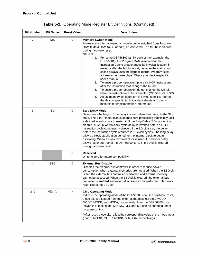
Program Control Unit
7 MS 0 Memory Switch ModeAllows some internal memory modules to be switched from Program RAM to data RAM (X, Y, or both) or vice versa. The MS bit is cleared during hardware reset.NOTES:
1. For some DSP56300 family devices (for example, the DSP56301), the Program RAM reserved for the Instruction Cache area changes its physical location in memory after the MS bit is set, because the instruction cache always uses the highest internal Program RAM addresses in those chips. Check your device-specific user’s manual.
2. To ensure proper operation, place six NOP instructions after the instruction that changes the MS bit.
3. To ensure proper operation, do not change the MS bit while the instruction cache is enabled (CE bit is set in SR).
4. Actual memory configuration is device-specific; refer to the device-specific technical data sheets and user’s manuals for implementation information.
6 SD 0 Stop Delay ModeDetermines the length of the delay invoked when the core exits the Stop state. The STOP instruction suspends core processing indefinitely until a defined event occurs to restart it. If the Stop Delay (SD) mode bit is cleared, a 128 K words clock cycle delay is invoked before a STOP instruction cycle continues. However, if the SD bit is set, the delay before the instruction cycle resumes is 16 clock cycles. The long delay allows a clock stabilization period for the internal clock to begin oscillating. When a stable external clock is used, the shorter delay allows faster start-up of the DSP56300 core. The SD bit is cleared during hardware reset.
5 0 ReservedWrite to zero for future compatibility.
4 EBD 0 External Bus DisableDisables the external bus controller in order to reduce power consumption when external memories are not used. When the EBD bit is set, the external bus controller is disabled and external memory cannot be accessed. When the EBD bit is cleared, the external bus controller is enabled and external access can be performed. Hardware reset clears the EBD bit.
3–0 M[D–A] * Chip Operating ModeIndicate the operating mode of the DSP56300 core. On hardware reset, these bits are loaded from the external mode select pins, MODD, MODC, MODB, and MODA, respectively. After the DSP56300 core leaves the Reset state, MD, MC, MB, and MA can be changed under program control.
*After reset, these bits reflect the corresponding value of the mode input (that is, MODD, MODC, MODB, or MODA, respectively).
Table 5-2. Operating Mode Register Bit Definitions (Continued)
Bit Number Bit Name Reset Value Description
5-10 DSP56300 Family Manual
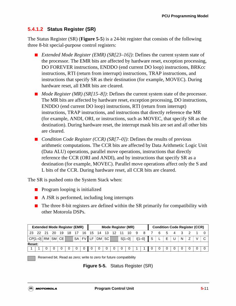
PCU Programming Model
5.4.1.2 Status Register (SR)
The Status Register (SR) (Figure 5-5) is a 24-bit register that consists of the following three 8-bit special-purpose control registers:
Extended Mode Register (EMR) (SR[23–16]): Defines the current system state of the processor. The EMR bits are affected by hardware reset, exception processing, DO FOREVER instructions, ENDDO (end current DO loop) instructions, BRKcc instructions, RTI (return from interrupt) instructions, TRAP instructions, and instructions that specify SR as their destination (for example, MOVEC). During hardware reset, all EMR bits are cleared.
Mode Register (MR) (SR[15–8]): Defines the current system state of the processor. The MR bits are affected by hardware reset, exception processing, DO instructions, ENDDO (end current DO loop) instructions, RTI (return from interrupt) instructions, TRAP instructions, and instructions that directly reference the MR (for example, ANDI, ORI, or instructions, such as MOVEC, that specify SR as the destination). During hardware reset, the interrupt mask bits are set and all other bits are cleared.
Condition Code Register (CCR) (SR[7–0]): Defines the results of previous arithmetic computations. The CCR bits are affected by Data Arithmetic Logic Unit (Data ALU) operations, parallel move operations, instructions that directly reference the CCR (ORI and ANDI), and by instructions that specify SR as a destination (for example, MOVEC). Parallel move operations affect only the S and L bits of the CCR. During hardware reset, all CCR bits are cleared.
The SR is pushed onto the System Stack when:
Program looping is initialized
A JSR is performed, including long interrupts
The three 8-bit registers are defined within the SR primarily for compatibility with other Motorola DSPs.
Figure 5-5. Status Register (SR)
Extended Mode Register (EMR) Mode Register (MR) Condition Code Register (CCR)
23 22 21 20 19 18 17 16 15 14 13 12 11 10 9 8 7 6 5 4 3 2 1 0
CP[1–0] RM SM CE SA FV LF DM SC S[1–0] I[1–0] S L E U N Z V C
Reset:1 1 0 0 0 0 0 0 0 0 0 0 0 0 1 1 0 0 0 0 0 0 0 0
Reserved bit. Read as zero; write to zero for future compatibility
Program Control Unit 5-11
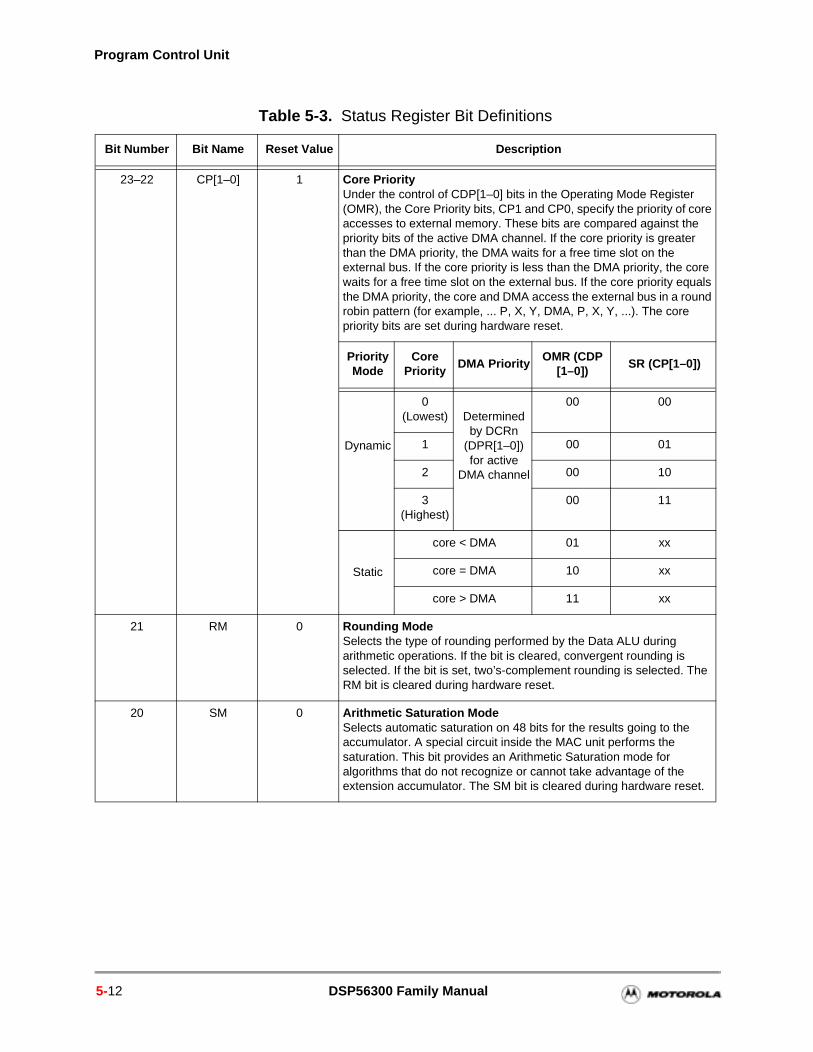
Program Control Unit
Table 5-3. Status Register Bit Definitions
Bit Number Bit Name Reset Value Description
23–22 CP[1–0] 1 Core PriorityUnder the control of CDP[1–0] bits in the Operating Mode Register (OMR), the Core Priority bits, CP1 and CP0, specify the priority of core accesses to external memory. These bits are compared against the priority bits of the active DMA channel. If the core priority is greater than the DMA priority, the DMA waits for a free time slot on the external bus. If the core priority is less than the DMA priority, the core waits for a free time slot on the external bus. If the core priority equals the DMA priority, the core and DMA access the external bus in a round robin pattern (for example, ... P, X, Y, DMA, P, X, Y, ...). The core priority bits are set during hardware reset.
Priority Mode
Core Priority
DMA PriorityOMR (CDP
[1–0])SR (CP[1–0])
Dynamic
0 (Lowest) Determined
by DCRn (DPR[1–0]) for active
DMA channel
00 00
1 00 01
2 00 10
3 (Highest)
00 11
Static
core < DMA 01 xx
core = DMA 10 xx
core > DMA 11 xx
21 RM 0 Rounding ModeSelects the type of rounding performed by the Data ALU during arithmetic operations. If the bit is cleared, convergent rounding is selected. If the bit is set, two’s-complement rounding is selected. The RM bit is cleared during hardware reset.
20 SM 0 Arithmetic Saturation ModeSelects automatic saturation on 48 bits for the results going to the accumulator. A special circuit inside the MAC unit performs the saturation. This bit provides an Arithmetic Saturation mode for algorithms that do not recognize or cannot take advantage of the extension accumulator. The SM bit is cleared during hardware reset.
5-12 DSP56300 Family Manual
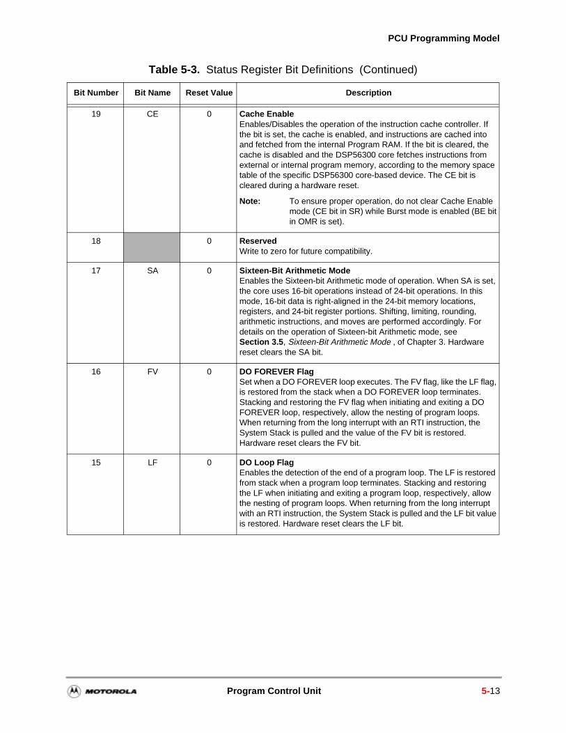
PCU Programming Model
19 CE 0 Cache EnableEnables/Disables the operation of the instruction cache controller. If the bit is set, the cache is enabled, and instructions are cached into and fetched from the internal Program RAM. If the bit is cleared, the cache is disabled and the DSP56300 core fetches instructions from external or internal program memory, according to the memory space table of the specific DSP56300 core-based device. The CE bit is cleared during a hardware reset.
Note: To ensure proper operation, do not clear Cache Enable mode (CE bit in SR) while Burst mode is enabled (BE bit in OMR is set).
18 0 ReservedWrite to zero for future compatibility.
17 SA 0 Sixteen-Bit Arithmetic ModeEnables the Sixteen-bit Arithmetic mode of operation. When SA is set, the core uses 16-bit operations instead of 24-bit operations. In this mode, 16-bit data is right-aligned in the 24-bit memory locations, registers, and 24-bit register portions. Shifting, limiting, rounding, arithmetic instructions, and moves are performed accordingly. For details on the operation of Sixteen-bit Arithmetic mode, see Section 3.5, Sixteen-Bit Arithmetic Mode , of Chapter 3. Hardware reset clears the SA bit.
16 FV 0 DO FOREVER FlagSet when a DO FOREVER loop executes. The FV flag, like the LF flag, is restored from the stack when a DO FOREVER loop terminates. Stacking and restoring the FV flag when initiating and exiting a DO FOREVER loop, respectively, allow the nesting of program loops. When returning from the long interrupt with an RTI instruction, the System Stack is pulled and the value of the FV bit is restored. Hardware reset clears the FV bit.
15 LF 0 DO Loop FlagEnables the detection of the end of a program loop. The LF is restored from stack when a program loop terminates. Stacking and restoring the LF when initiating and exiting a program loop, respectively, allow the nesting of program loops. When returning from the long interrupt with an RTI instruction, the System Stack is pulled and the LF bit value is restored. Hardware reset clears the LF bit.
Table 5-3. Status Register Bit Definitions (Continued)
Bit Number Bit Name Reset Value Description
Program Control Unit 5-13
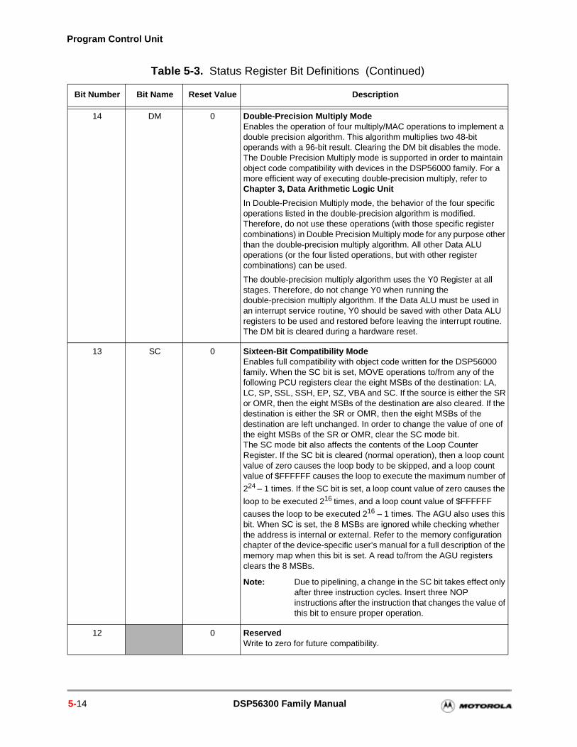
Program Control Unit
14 DM 0 Double-Precision Multiply ModeEnables the operation of four multiply/MAC operations to implement a double precision algorithm. This algorithm multiplies two 48-bit operands with a 96-bit result. Clearing the DM bit disables the mode. The Double Precision Multiply mode is supported in order to maintain object code compatibility with devices in the DSP56000 family. For a more efficient way of executing double-precision multiply, refer to Chapter 3, Data Arithmetic Logic Unit
In Double-Precision Multiply mode, the behavior of the four specific operations listed in the double-precision algorithm is modified. Therefore, do not use these operations (with those specific register combinations) in Double Precision Multiply mode for any purpose other than the double-precision multiply algorithm. All other Data ALU operations (or the four listed operations, but with other register combinations) can be used.
The double-precision multiply algorithm uses the Y0 Register at all stages. Therefore, do not change Y0 when running the double-precision multiply algorithm. If the Data ALU must be used in an interrupt service routine, Y0 should be saved with other Data ALU registers to be used and restored before leaving the interrupt routine. The DM bit is cleared during a hardware reset.
13 SC 0 Sixteen-Bit Compatibility ModeEnables full compatibility with object code written for the DSP56000 family. When the SC bit is set, MOVE operations to/from any of the following PCU registers clear the eight MSBs of the destination: LA, LC, SP, SSL, SSH, EP, SZ, VBA and SC. If the source is either the SR or OMR, then the eight MSBs of the destination are also cleared. If the destination is either the SR or OMR, then the eight MSBs of the destination are left unchanged. In order to change the value of one of the eight MSBs of the SR or OMR, clear the SC mode bit.The SC mode bit also affects the contents of the Loop Counter Register. If the SC bit is cleared (normal operation), then a loop count value of zero causes the loop body to be skipped, and a loop count value of $FFFFFF causes the loop to execute the maximum number of
224 – 1 times. If the SC bit is set, a loop count value of zero causes the
loop to be executed 216 times, and a loop count value of $FFFFFF
causes the loop to be executed 216 – 1 times. The AGU also uses this bit. When SC is set, the 8 MSBs are ignored while checking whether the address is internal or external. Refer to the memory configuration chapter of the device-specific user’s manual for a full description of the memory map when this bit is set. A read to/from the AGU registers clears the 8 MSBs.
Note: Due to pipelining, a change in the SC bit takes effect only after three instruction cycles. Insert three NOP instructions after the instruction that changes the value of this bit to ensure proper operation.
12 0 ReservedWrite to zero for future compatibility.
Table 5-3. Status Register Bit Definitions (Continued)
Bit Number Bit Name Reset Value Description
5-14 DSP56300 Family Manual
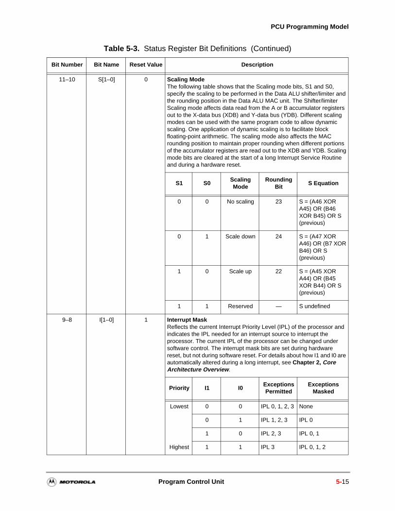
PCU Programming Model
11–10 S[1–0] 0 Scaling ModeThe following table shows that the Scaling mode bits, S1 and S0, specify the scaling to be performed in the Data ALU shifter/limiter and the rounding position in the Data ALU MAC unit. The Shifter/limiter Scaling mode affects data read from the A or B accumulator registers out to the X-data bus (XDB) and Y-data bus (YDB). Different scaling modes can be used with the same program code to allow dynamic scaling. One application of dynamic scaling is to facilitate block floating-point arithmetic. The scaling mode also affects the MAC rounding position to maintain proper rounding when different portions of the accumulator registers are read out to the XDB and YDB. Scaling mode bits are cleared at the start of a long Interrupt Service Routine and during a hardware reset.
S1 S0Scaling Mode
Rounding Bit
S Equation
0 0 No scaling 23 S = (A46 XOR A45) OR (B46 XOR B45) OR S (previous)
0 1 Scale down 24 S = (A47 XOR A46) OR (B7 XOR B46) OR S (previous)
1 0 Scale up 22 S = (A45 XOR A44) OR (B45 XOR B44) OR S (previous)
1 1 Reserved — S undefined
9–8 I[1–0] 1 Interrupt MaskReflects the current Interrupt Priority Level (IPL) of the processor and indicates the IPL needed for an interrupt source to interrupt the processor. The current IPL of the processor can be changed under software control. The interrupt mask bits are set during hardware reset, but not during software reset. For details about how I1 and I0 are automatically altered during a long interrupt, see Chapter 2, Core Architecture Overview.
Priority I1 I0Exceptions Permitted
Exceptions Masked
Lowest 0 0 IPL 0, 1, 2, 3 None
0 1 IPL 1, 2, 3 IPL 0
1 0 IPL 2, 3 IPL 0, 1
Highest 1 1 IPL 3 IPL 0, 1, 2
Table 5-3. Status Register Bit Definitions (Continued)
Bit Number Bit Name Reset Value Description
Program Control Unit 5-15
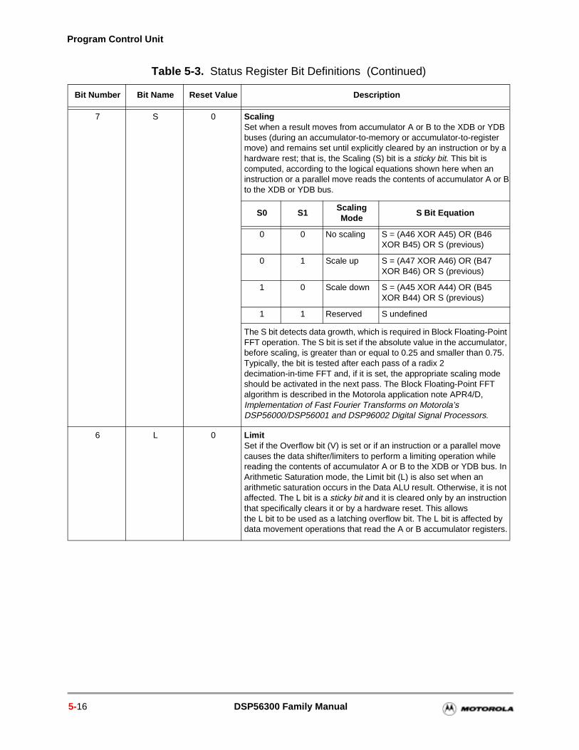
Program Control Unit
7 S 0 ScalingSet when a result moves from accumulator A or B to the XDB or YDB buses (during an accumulator-to-memory or accumulator-to-register move) and remains set until explicitly cleared by an instruction or by a hardware rest; that is, the Scaling (S) bit is a sticky bit. This bit is computed, according to the logical equations shown here when an instruction or a parallel move reads the contents of accumulator A or Bto the XDB or YDB bus.
S0 S1Scaling Mode
S Bit Equation
0 0 No scaling S = (A46 XOR A45) OR (B46 XOR B45) OR S (previous)
0 1 Scale up S = (A47 XOR A46) OR (B47 XOR B46) OR S (previous)
1 0 Scale down S = (A45 XOR A44) OR (B45 XOR B44) OR S (previous)
1 1 Reserved S undefined
The S bit detects data growth, which is required in Block Floating-Point FFT operation. The S bit is set if the absolute value in the accumulator, before scaling, is greater than or equal to 0.25 and smaller than 0.75. Typically, the bit is tested after each pass of a radix 2 decimation-in-time FFT and, if it is set, the appropriate scaling mode should be activated in the next pass. The Block Floating-Point FFT algorithm is described in the Motorola application note APR4/D, Implementation of Fast Fourier Transforms on Motorola’s DSP56000/DSP56001 and DSP96002 Digital Signal Processors.
6 L 0 LimitSet if the Overflow bit (V) is set or if an instruction or a parallel move causes the data shifter/limiters to perform a limiting operation while reading the contents of accumulator A or B to the XDB or YDB bus. In Arithmetic Saturation mode, the Limit bit (L) is also set when an arithmetic saturation occurs in the Data ALU result. Otherwise, it is not affected. The L bit is a sticky bit and it is cleared only by an instruction that specifically clears it or by a hardware reset. This allowsthe L bit to be used as a latching overflow bit. The L bit is affected by data movement operations that read the A or B accumulator registers.
Table 5-3. Status Register Bit Definitions (Continued)
Bit Number Bit Name Reset Value Description
5-16 DSP56300 Family Manual
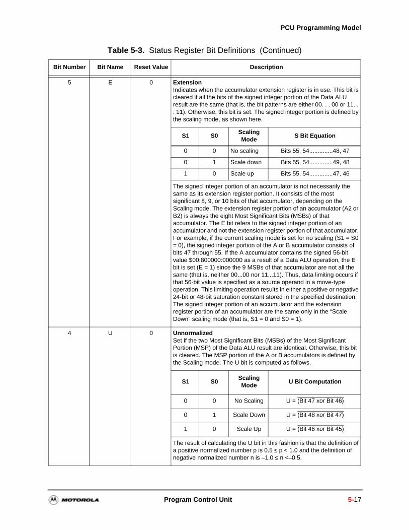
PCU Programming Model
5 E 0 ExtensionIndicates when the accumulator extension register is in use. This bit is cleared if all the bits of the signed integer portion of the Data ALU result are the same (that is, the bit patterns are either 00. . . 00 or 11. . . 11). Otherwise, this bit is set. The signed integer portion is defined by the scaling mode, as shown here.
S1 S0Scaling Mode
S Bit Equation
0 0 No scaling Bits 55, 54..............48, 47
0 1 Scale down Bits 55, 54..............49, 48
1 0 Scale up Bits 55, 54..............47, 46
The signed integer portion of an accumulator is not necessarily the same as its extension register portion. It consists of the most significant 8, 9, or 10 bits of that accumulator, depending on the Scaling mode. The extension register portion of an accumulator (A2 or B2) is always the eight Most Significant Bits (MSBs) of that accumulator. The E bit refers to the signed integer portion of an accumulator and not the extension register portion of that accumulator. For example, if the current scaling mode is set for no scaling (S1 = S0 = 0), the signed integer portion of the A or B accumulator consists of bits 47 through 55. If the A accumulator contains the signed 56-bit value $00:800000:000000 as a result of a Data ALU operation, the E bit is set (E = 1) since the 9 MSBs of that accumulator are not all the same (that is, neither 00...00 nor 11...11). Thus, data limiting occurs if that 56-bit value is specified as a source operand in a move-type operation. This limiting operation results in either a positive or negative 24-bit or 48-bit saturation constant stored in the specified destination. The signed integer portion of an accumulator and the extension register portion of an accumulator are the same only in the “Scale Down” scaling mode (that is, S1 = 0 and S0 = 1).
4 U 0 UnnormalizedSet if the two Most Significant Bits (MSBs) of the Most Significant Portion (MSP) of the Data ALU result are identical. Otherwise, this bit is cleared. The MSP portion of the A or B accumulators is defined by the Scaling mode. The U bit is computed as follows.
S1 S0Scaling Mode
U Bit Computation
0 0 No Scaling U = (Bit 47 xor Bit 46)
0 1 Scale Down U = (Bit 48 xor Bit 47)
1 0 Scale Up U = (Bit 46 xor Bit 45)
The result of calculating the U bit in this fashion is that the definition of a positive normalized number p is 0.5 ≤ p < 1.0 and the definition of negative normalized number n is –1.0 ≤ n <–0.5.
Table 5-3. Status Register Bit Definitions (Continued)
Bit Number Bit Name Reset Value Description
Program Control Unit 5-17
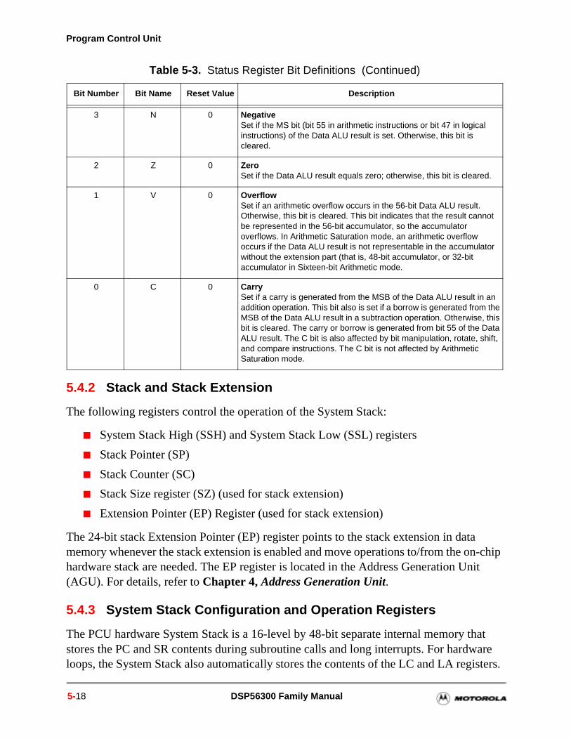
Program Control Unit
5.4.2 Stack and Stack Extension
The following registers control the operation of the System Stack:
System Stack High (SSH) and System Stack Low (SSL) registers
Stack Pointer (SP)
Stack Counter (SC)
Stack Size register (SZ) (used for stack extension)
Extension Pointer (EP) Register (used for stack extension)
The 24-bit stack Extension Pointer (EP) register points to the stack extension in data memory whenever the stack extension is enabled and move operations to/from the on-chip hardware stack are needed. The EP register is located in the Address Generation Unit (AGU). For details, refer to Chapter 4, Address Generation Unit.
5.4.3 System Stack Configuration and Operation Registers
The PCU hardware System Stack is a 16-level by 48-bit separate internal memory that stores the PC and SR contents during subroutine calls and long interrupts. For hardware loops, the System Stack also automatically stores the contents of the LC and LA registers.
3 N 0 NegativeSet if the MS bit (bit 55 in arithmetic instructions or bit 47 in logical instructions) of the Data ALU result is set. Otherwise, this bit is cleared.
2 Z 0 ZeroSet if the Data ALU result equals zero; otherwise, this bit is cleared.
1 V 0 OverflowSet if an arithmetic overflow occurs in the 56-bit Data ALU result. Otherwise, this bit is cleared. This bit indicates that the result cannot be represented in the 56-bit accumulator, so the accumulator overflows. In Arithmetic Saturation mode, an arithmetic overflow occurs if the Data ALU result is not representable in the accumulator without the extension part (that is, 48-bit accumulator, or 32-bit accumulator in Sixteen-bit Arithmetic mode.
0 C 0 CarrySet if a carry is generated from the MSB of the Data ALU result in an addition operation. This bit also is set if a borrow is generated from the MSB of the Data ALU result in a subtraction operation. Otherwise, this bit is cleared. The carry or borrow is generated from bit 55 of the Data ALU result. The C bit is also affected by bit manipulation, rotate, shift, and compare instructions. The C bit is not affected by Arithmetic Saturation mode.
Table 5-3. Status Register Bit Definitions (Continued)
Bit Number Bit Name Reset Value Description
5-18 DSP56300 Family Manual
PCU Programming Model
ction
oes
by the
s bit is one
ystem kable
of ble r Y
All other data and control register contents can be stored in the System Stack via software control. Each location in the System Stack is addressable as two 24-bit registers, System Stack High (SSH) and System Stack Low (SSL), to which the four LSBs of the SP register collectively point. The System Stack is extended in the data memory in a space specified by the stack control registers that monitor System Stack accesses. This hardware copies the Least Recently Used (LRU) location of the System Stack to data memory if the on-chip hardware stack is full and brings data from data memory when the on-chip hardware stack is empty. The main tasks performed by the System Stack include:
Storing return address and status for subroutine calls (including long interrupts)
Storing LA, LC, PC, and SR for the hardware DO loops
When a subroutine is called (for example, using the JSR instruction), the return address (PC) is automatically stored in the SSH, and the status register (SR) is automatically stored in the SSL. When the RTS instruction initiates a return from the subroutine, the contents of the top location in the SSH are pulled and loaded into the PC, and the SR is not affected. When the RTI instruction initiates a return, the contents of the top location in the System Stack are pulled and loaded into the PC and SR (from SSH and SSL, respectively).
The System Stack is also used to implement no-overhead nested hardware DO loops. When a hardware DO loop is initiated (for example, by using the DO instruction), the previous contents of the LC Register are automatically stored in the SSL, the previous contents of the LA Register are automatically stored in the SSH, and the Stack Pointer (SP) is incremented. After the SP is incremented, the address of the loop’s first instru(PC) is also stored in the SSH, and the SR is stored in the SSL.
Note: Moving data to or from SSH increments or decrements the SP. The SSL dnot affect the SP.
The System Stack can be extended into 24-bit wide X or Y data memory via controlhardware that monitors the accesses to the System Stack. This extension is enabledStack Extension Enable (SEN) bit in the chip Operating Mode Register (OMR). If thiis cleared, the extension of the system stack is disabled, and the amount of nesting determined by the limited size of the hardware stack (that is, 15 available locations; location is unusable when the stack extension is disabled). The System Stack can accommodate up to 15 long interrupts, seven DO loops, or 15 JSRs, (or equivalent combinations of these) when its extension into data memory is disabled. When the SStack limit is exceeded (either in Extended or in the Non-extended mode), a nonmasstack error interrupt occurs. By enabling the Stack extension, the limits on the level nesting of subroutines or DO loops can be set to any desired value, subject to availainternal/external memory. The XYS bit in the OMR Register determines whether X odata memory is used.
Program Control Unit 5-19
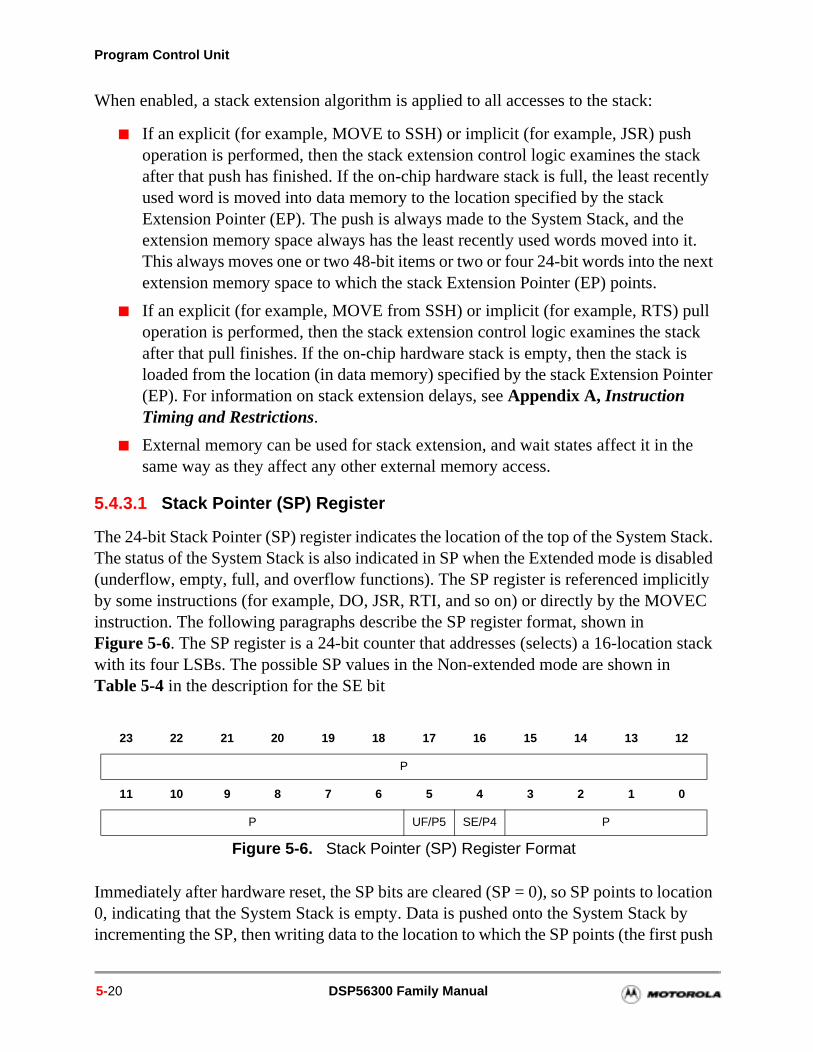
Program Control Unit
When enabled, a stack extension algorithm is applied to all accesses to the stack:
If an explicit (for example, MOVE to SSH) or implicit (for example, JSR) push operation is performed, then the stack extension control logic examines the stack after that push has finished. If the on-chip hardware stack is full, the least recently used word is moved into data memory to the location specified by the stack Extension Pointer (EP). The push is always made to the System Stack, and the extension memory space always has the least recently used words moved into it. This always moves one or two 48-bit items or two or four 24-bit words into the next extension memory space to which the stack Extension Pointer (EP) points.
If an explicit (for example, MOVE from SSH) or implicit (for example, RTS) pull operation is performed, then the stack extension control logic examines the stack after that pull finishes. If the on-chip hardware stack is empty, then the stack is loaded from the location (in data memory) specified by the stack Extension Pointer (EP). For information on stack extension delays, see Appendix A, Instruction Timing and Restrictions.
External memory can be used for stack extension, and wait states affect it in the same way as they affect any other external memory access.
5.4.3.1 Stack Pointer (SP) Register
The 24-bit Stack Pointer (SP) register indicates the location of the top of the System Stack. The status of the System Stack is also indicated in SP when the Extended mode is disabled (underflow, empty, full, and overflow functions). The SP register is referenced implicitly by some instructions (for example, DO, JSR, RTI, and so on) or directly by the MOVEC instruction. The following paragraphs describe the SP register format, shown in Figure 5-6. The SP register is a 24-bit counter that addresses (selects) a 16-location stack with its four LSBs. The possible SP values in the Non-extended mode are shown in Table 5-4 in the description for the SE bit
Immediately after hardware reset, the SP bits are cleared (SP = 0), so SP points to location 0, indicating that the System Stack is empty. Data is pushed onto the System Stack by incrementing the SP, then writing data to the location to which the SP points (the first push
23 22 21 20 19 18 17 16 15 14 13 12
P
11 10 9 8 7 6 5 4 3 2 1 0
P UF/P5 SE/P4 P
Figure 5-6. Stack Pointer (SP) Register Format
5-20 DSP56300 Family Manual
PCU Programming Model
after reset is to location 1). An item is pulled off the stack by copying it from the location to which the SP points and then decrementing SP.
Table 5-4. Stack Pointer (SP) Register Bit Definitions
Bit Number Bit Name Reset Value Description
23–6 P[23–6] 0 P[23–6]In extended mode, these bits act as bits 6 through 23 of the Stack Pointer as part of a 24-bit up/down counter.
5 UF/PF 0 Underflow Flag / P5In the Extended mode, UF acts as bit 5 of the Stack Pointer as part of a 24-bit up/down counter. In the Non-extended mode, UF is set when a stack underflow occurs. The stack UF is a sticky bit (that is, once the Stack Error flag is set, the UF does not change state until explicitly written by a MOVE instruction). The combination of “underflow = 1” and “stack error = 0” is an illegal combination and does not occur unless you force it. Also see the description for the Stack Error flag.
Program Control Unit 5-21
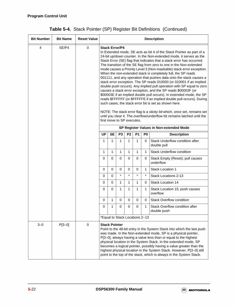
Program Control Unit
4 SE/P4 0 Stack Error/P4In Extended mode, SE acts as bit 4 of the Stack Pointer as part of a 24-bit up/down counter. In the Non-extended mode, it serves as the Stack Error (SE) flag that indicates that a stack error has occurred. The transition of the SE flag from zero to one in the Non-extended mode causes a Priority Level 3 (Non-maskable) stack error exception. When the non-extended stack is completely full, the SP reads 001111, and any operation that pushes data onto the stack causes a stack error exception. The SP reads 010000 (or 010001 if an implied double push occurs). Any implied pull operation with SP equal to zero causes a stack error exception, and the SP reads $00003F (or $00003E if an implied double pull occurs). In extended mode, the SP reads $FFFFFF (or $FFFFFE if an implied double pull occurs). During such cases, the stack error bit is set as shown here.
NOTE: The stack error flag is a sticky bit which, once set, remains set until you clear it. The overflow/underflow bit remains latched until the first move to SP executes.
SP Register Values in Non-extended Mode
UF SE P3 P2 P1 P0 Description
1 1 1 1 1 0 Stack Underflow condition after double pull
1 1 1 1 1 1 Stack Underflow condition
0 0 0 0 0 0 Stack Empty (Reset); pull causes underflow
0 0 0 0 0 1 Stack Location 1
0 0 * * * * Stack Locations 2-13
0 0 1 1 1 0 Stack Location 14
0 0 1 1 1 1 Stack Location 15; push causes overflow
0 1 0 0 0 0 Stack Overflow condition
0 1 0 0 0 1 Stack Overflow condition after double push
*Equal to Stack Locations 2–13
3–0 P[3–0] 0 Stack PointerPoint to the 48-bit entry in the System Stack into which the last push was made. In the Non-extended mode, SP is a physical pointer, P[3–0], always having a value less than or equal to the highest physical location in the System Stack. In the extended mode, SP becomes a logical pointer, possibly having a value greater than the highest physical location in the System Stack. However, P[3–0] still point to the top of the stack, which is always in the System Stack.
Table 5-4. Stack Pointer (SP) Register Bit Definitions (Continued)
Bit Number Bit Name Reset Value Description
5-22 DSP56300 Family Manual
PCU Programming Model
5.4.3.2 Stack Counter (SC) Register
The 5-bit Stack Counter (SC) register monitors how many entries of the hardware stack are in use. The SC is a read/write register and is referenced implicitly by some instructions (for example, DO, JSR, and RTI) or directly by the MOVEC instruction. The stack counter register is cleared during hardware reset. During normal operation, do not write to the SC register. If a task switch is needed, writing a value greater than 14 or smaller than 2 automatically activates the stack extension control hardware. For proper operation, the SC should not be written with values greater than 16.
5.4.3.3 Stack Size (SZ) Register
The 24-bit Stack Size (SZ) register determines the number of data words allocated in memory for the stack in the Extended mode. The necessary value of the SZ register can be determined by SZ = 15 + software_buffer_size / 2, where the buffer size is the number of 24-bit words allocated for the stack extension in data memory. (Fifteen is the maximum number of 48-bit entries that can be occupied in the 16-entry hardware stack at any given time.) The extended stack overflow flag is generated when the value in SP equals the value in SZ and then a push is done.
Note: A stack exception can occur only when the stack is used in Non-extended mode.
The SZ register is not initialized during hardware reset, and must be set, using a MOVEC instruction, prior to enabling the stack extension.
5.4.4 Program, Loop, and Exception Processing Control
The code execution flow control is performed using four registers in the PCU:
Program Counter (PC) Register
Loop Address (LA) Register
Loop Counter (LC) Register
Vector Base Address (VBA) Register
5.4.4.1 Program Counter (PC) Register
The Program Counter (PC) Register is a special-purpose 24-bit address register that contains the address of instruction words in the program memory space. The PC can point to instructions, data operands, or addresses of operands. References to this register are always inherent and are implied by most instructions. The PC is stacked when hardware loops are initialized, when a JSR is performed, or when a long interrupt occurs. The PC is the source for the calculation of the real address in all position-independent instructions (such as the instruction BRA).
Program Control Unit 5-23
Program Control Unit
n the
–0] pt
bits
he
5.4.4.2 Loop Address (LA) Register
The contents of the 24-bit Loop Address (LA) register indicate the location of the last instruction word in a hardware loop. This register is stacked into the SSH by a DO instruction and is unstacked either by end-of-loop processing or by execution of ENDDO and BRKcc instructions. The LA register, a read/write register, is written by a DO instruction and read by the System Stack when the register is stacked.
5.4.4.3 Loop Counter (LC) Register
The Loop Counter (LC) register is a special read/write 24-bit counter that specifies the number of times a hardware program loop repeats, in the range of 0 to (224 – 1). This register is stacked into the SSL by a DO instruction and unstacked by end-of-loop processing or by execution of ENDDO and BRKcc instructions. The LC is also used iREP instruction to specify how many times to repeat the repeated instruction.
5.4.4.4 Vector Base Address (VBA) Register
The Vector Base Address Register (VBA) is a 24-bit register. Eight of the bits VBA[7are read-only and always cleared. The VBA is used as a base address of the interruvector table (discussed in Chapter 2, Core Architecture Overview). When a fast or long interrupt executes, VBA[7– 0] are driven from the program interrupt control unit, and23–8 are driven from the VBA. The VBA Register is a read/write register that is referenced implicitly by interrupt processing or directly by the MOVEC instruction. TVBA is cleared during hardware reset.
5-24 DSP56300 Family Manual
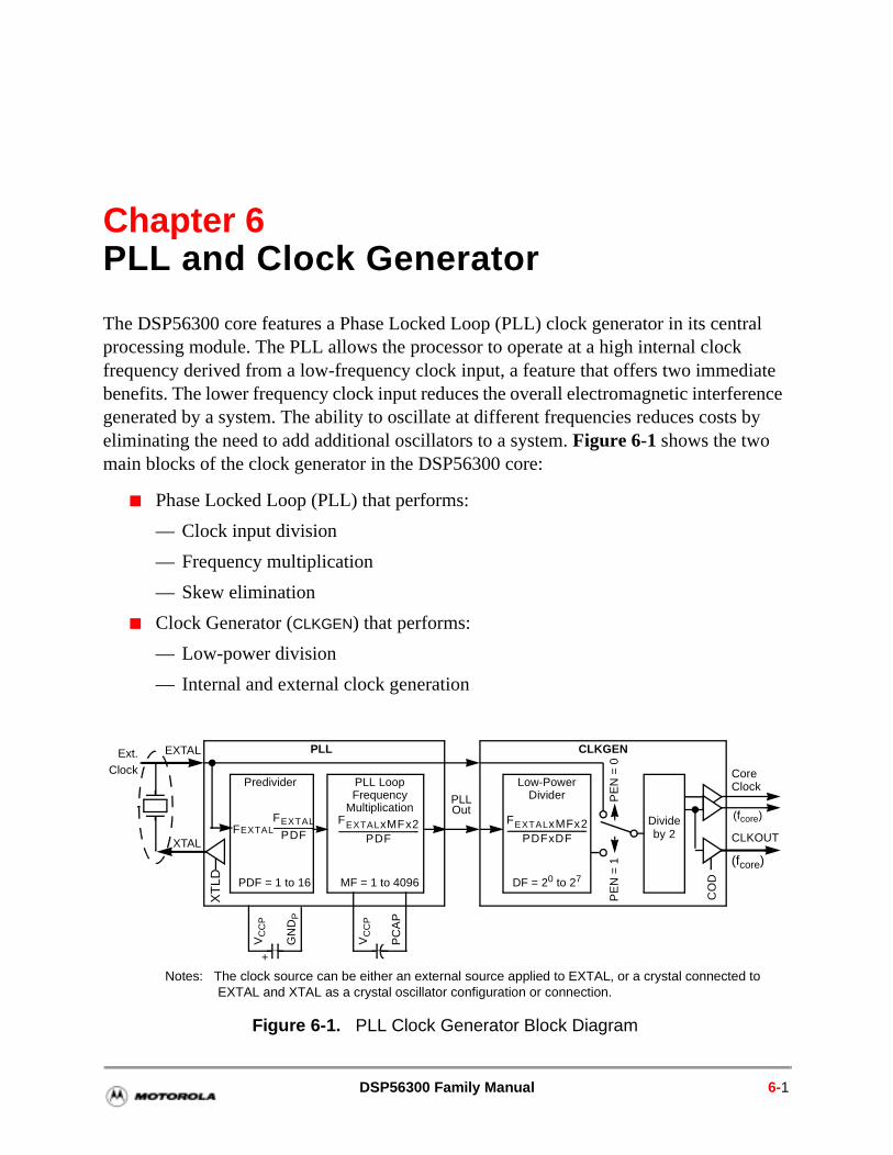
Chapter 6PLL and Clock Generator
The DSP56300 core features a Phase Locked Loop (PLL) clock generator in its central processing module. The PLL allows the processor to operate at a high internal clock frequency derived from a low-frequency clock input, a feature that offers two immediate benefits. The lower frequency clock input reduces the overall electromagnetic interference generated by a system. The ability to oscillate at different frequencies reduces costs by eliminating the need to add additional oscillators to a system. Figure 6-1 shows the two main blocks of the clock generator in the DSP56300 core:
Phase Locked Loop (PLL) that performs:
— Clock input division
— Frequency multiplication
— Skew elimination
Clock Generator (CLKGEN) that performs:
— Low-power division
— Internal and external clock generation
Figure 6-1. PLL Clock Generator Block Diagram
EXTAL
XTAL
Ext.
Notes: The clock source can be either an external source applied to EXTAL, or a crystal connected to EXTAL and XTAL as a crystal oscillator configuration or connection.
PLL CLKGEN
PLL
Core
CLKOUT
Predivider
PDF = 1 to 16
PLL LoopFrequency
Multiplication
MF = 1 to 4096
Low-PowerDivider
Divideby 2
PE
N =
1
DF = 20 to 27
FEXTAL
PDF---------------------
FEXTALxMFx2PDF
-----------------------------------------FEXTALxMFx2
PDFxDF------------------------------------FEXTAL
Clock
Out
Clock
PE
N =
0
CO
D
XT
LD
GN
DP
VC
CP
+
PC
AP
VC
CP
(fcore)
(fcore)
DSP56300 Family Manual 6-1
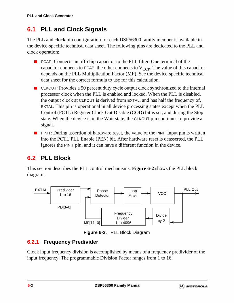
PLL and Clock Generator
6.1 PLL and Clock Signals
The PLL and clock pin configuration for each DSP56300 family member is available in the device-specific technical data sheet. The following pins are dedicated to the PLL and clock operation:
PCAP: Connects an off-chip capacitor to the PLL filter. One terminal of the capacitor connects to PCAP, the other connects to VCCP. The value of this capacitor depends on the PLL Multiplication Factor (MF). See the device-specific technical data sheet for the correct formula to use for this calculation.
CLKOUT: Provides a 50 percent duty cycle output clock synchronized to the internal processor clock when the PLL is enabled and locked. When the PLL is disabled, the output clock at CLKOUT is derived from EXTAL, and has half the frequency of, EXTAL. This pin is operational in all device processing states except when the PLL Control (PCTL) Register Clock Out Disable (COD) bit is set, and during the Stop state. When the device is in the Wait state, the CLKOUT pin continues to provide a signal.
PINIT: During assertion of hardware reset, the value of the PINIT input pin is written into the PCTL PLL Enable (PEN) bit. After hardware reset is deasserted, the PLL ignores the PINIT pin, and it can have a different function in the device.
6.2 PLL Block
This section describes the PLL control mechanisms. Figure 6-2 shows the PLL block diagram.
6.2.1 Frequency Predivider
Clock input frequency division is accomplished by means of a frequency predivider of the input frequency. The programmable Division Factor ranges from 1 to 16.
Figure 6-2. PLL Block Diagram
PhaseDetector
LoopFilter VCO
FrequencyDivider
1 to 4096
PLL OutEXTAL
MF[11–0]
Predivider
PD[3–0]
1 to 16
Divideby 2
6-2 DSP56300 Family Manual
PLL Block
6.2.2 Phase Detector and Charge Pump Loop Filter
The Phase Detector (PD) detects any phase difference between the external clock (EXTAL) and the phase of the clock generated by the frequency divider. At the point where there is negligible phase difference and the frequency of the two inputs is identical, the PLL is in the Locked state. The charge pump loop filter receives signals from the PD and either increases or decreases the phase based on the PD signals. An external capacitor is connected to the PCAP input to determine low pass filter corner frequencies. The value of this capacitor depends on the Multiplication Factor (MF) of the PLL. See the Specifications section in the device-specific technical data sheet for the formula to determine the proper value for the PLL capacitor. After the PLL locks onto the proper phase and frequency, it reverts to the Narrow Bandwidth mode, which is useful for tracking small changes due to frequency drift of the EXTAL clock.
6.2.3 Voltage Controlled Oscillator (VCO)
The Voltage Controlled Oscillator (VCO) can oscillate at frequencies from the minimum speed up to the maximum allowed clock input frequency. See the device-specific technical data sheet for these speeds.
Note: When the PLL is enabled, the device operating frequency is half of the VCO oscillating frequency.
If EXTAL is less than the VCO minimum working frequency, the hardware design should hold the PINIT input low during hardware reset. Following reset, the software can change MF to the desired value, and set the PCTL[PEN] bit.
6.2.3.1 Divide by 2
As part of the PLL feedback loop, the output of the VCO is divided by 2. The resulting constant multiplication by 2 of the VCO/PLL output allows for the generation of the special internal clock phases required by the device.
6.2.3.2 Frequency Divider
The Frequency Divider portion of the PLL feedback loop divides the VCO output by a programmable 12-bit value before entering the Phase Detector. The net result is a multiplication of the incoming external clock by the programmed value. This is called the Multiplication Factor and is programmed using the PCTL[MF] bits. The Multiplication Factor can range from 1 to 4096.
PLL and Clock Generator 6-3
PLL and Clock Generator
on in
es of
rnal
6.2.3.3 PLL Control Elements
The PLL uses three major control elements in its circuitry:
Clock input division
Frequency multiplication
Skew elimination
6.2.3.3.1 Clock Input Division
The PLL can divide the input frequency by any integer between 1 and 16. The combination of input division and output low-power division enables you to generate almost every frequency value out of the PLL (see Section 6.2.3.4.3, Operating Frequency, on page 6-6). The Division Factor can be modified by changing the value of the PCTL Predivider Factor (PDF) bits (PD[3–0]). The output frequency of the predivider is determined using the following formula:
6.2.3.3.2 Frequency Multiplication
The PLL can multiply the input frequency by any integer between 1 and 4096. The Multiplication Factor can be modified by changing the value of the PCTL MultiplicatiFactor (MF[11–0]) bits. The output frequency of the PLL (that is, PLL Out as shown Figure 6-1 on page 6-1) is computed using the following formula:
6.2.3.3.3 Skew Elimination
The phase skew of the PLL is defined as the time difference between the falling edgEXTAL and CLKOUT for a given capacitive load on CLKOUT, over the entire process, temperature, and voltage ranges. The PLL can eliminate the skew between the exteclock (EXTAL), the internal clock phases, and the CLKOUT signal, allowing tighter synchronous timings. Skew elimination is active only when the PLL is enabled and programmed with a Multiplication Factor less than or equal to 4. When the PLL is disabled, or when the Multiplication Factor is greater than 4, clock skew can exist.
Note: Skew elimination is assured only if EXTAL is greater than the minimum frequency specified in the device-specific technical data sheet (typically 15MHz).
FextalPDF
---------------FEXTAL
Fextal MF × 2×PDF
------------------------------------------FEXTAL
6-4 DSP56300 Family Manual

PLL Block
is a as the PLL
the y
y the
6.2.3.4 Clock Generator
Figure 6-3 shows the Clock Generator block diagram. The components of the Clock Generator are described in the following sections.
6.2.3.4.1 Low-Power Divider (LPD)
The Clock Generator has a divider connected to the output of the PLL. The Low-Power Divider (LPD) divides the output frequency of the VCO by any power of 2 from 20 to 27. The Division Factor (DF) of the LPD can be modified by changing the value of the PLL Control Register (PCTL) Division Factor bits DF[2–0]. Since the LPD is not in the closedloop of the PLL, changes in the DF do not cause a loss of lock condition. The result significant power savings when the LPD operates in low-power consumption modes device is not involved in intensive calculations. When the device is required to exit alow-power mode, it can immediately do so with no time needed for clock recovery or lock.
6.2.3.4.2 Internal and External Clock Pulse Generator
The output stage of the Clock Generator generates the clock signals to the core anddevice peripherals, and drives the CLKOUT pin. The output stage divides the frequency btwo. The input source to the output stage is selected between:
EXTAL (PEN = 0, PLL disabled), which generates a device frequency defined bfollowing formula:
Low-Power Divider output (PEN = 1, PLL enabled), which generates a devicefrequency defined by the following formula:
Figure 6-3. CLKGEN Block Diagram
EXTAL
Low-PowerDivider
DF[2–0]
20 to 27
PLL OUT
Divide by 2
Core Clock
CLKOUT
2-Phase
(FCORE)
(FCORE)
Fextal2
---------------FEXTAL
FEXTAL MF×PDF DF×
---------------------------------------FEXTAL
PLL and Clock Generator 6-5

PLL and Clock Generator
X I/O
6.2.3.4.3 Operating Frequency
When PEN = 1, the operating frequency of the core is governed by the frequency control bits in the PCTL Register according to the following formula:
where:
MF is the Multiplication Factor defined by MF[11–0]
PDF is the Predivider Factor defined by PD[3–0]
DF is the Division Factor defined by DF[2–0]
FCORE is the device operating frequency
FEXTAL is the external EXTAL input
6.3 PLL Programming Model
The PLL clock generator uses a single register, the PCTL Register. The PCTL is an mapped 24-bit read/write register used to direct the operation of the on-chip PLL. Figure 6-4 shows the PCTL control bits.
Figure 6-4. PLL Control (PCTL) Register
FCORE
FEXTAL MF×
PDF DF ×--------------------------------------=FEXTAL
23 22 21 20 19 18 17 16 15 14 13 12
PD3 PD2 PD1 PD0 COD PEN PSTP XTLD XTLR DF2 DF1 DF0
Reset:
a a a a 0 b 0 a a 0 0 0
11 10 9 8 7 6 5 4 3 2 1 0
MF11 MF10 MF9 MF8 MF7 MF6 MF5 MF4 MF3 MF2 MF1 MF0
Reset:
a a a a a a a a a a a a
ab
The reset value is implementation dependent and is listed in the device-specific user’s manual.The reset value of the PEN bit is based on the value of the PLL PINIT input.
6-6 DSP56300 Family Manual
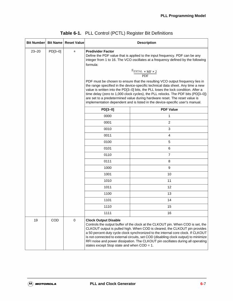
PLL Programming Model
Table 6-1. PLL Control (PCTL) Register Bit Definitions
Bit Number Bit Name Reset Value Description
23–20 PD[3–0] a Predivider FactorDefine the PDF value that is applied to the input frequency. PDF can be any integer from 1 to 16. The VCO oscillates at a frequency defined by the following formula:
PDF must be chosen to ensure that the resulting VCO output frequency lies in the range specified in the device-specific technical data sheet. Any time a new value is written into the PD[3–0] bits, the PLL loses the lock condition. After a time delay (zero to 1,000 clock cycles), the PLL relocks. The PDF bits (PD[3–0]) are set to a predetermined value during hardware reset. The reset value is implementation dependent and is listed in the device-specific user’s manual.
PD[3–0] PDF Value
0000 1
0001 2
0010 3
0011 4
0100 5
0101 6
0110 7
0111 8
1000 9
1001 10
1010 11
1011 12
1100 13
1101 14
1110 15
1111 16
19 COD 0 Clock Output DisableControls the output buffer of the clock at the CLKOUT pin. When COD is set, the CLKOUT output is pulled high. When COD is cleared, the CLKOUT pin provides a 50 percent duty cycle clock synchronized to the internal core clock. If CLKOUT is not connected to external circuits, set COD (disabling clock output) to minimize RFI noise and power dissipation. The CLKOUT pin oscillates during all operating states except Stop state and when COD = 1.
Fextal MF× 2×PDF
----------------------------------------FEXTAL
PLL and Clock Generator 6-7
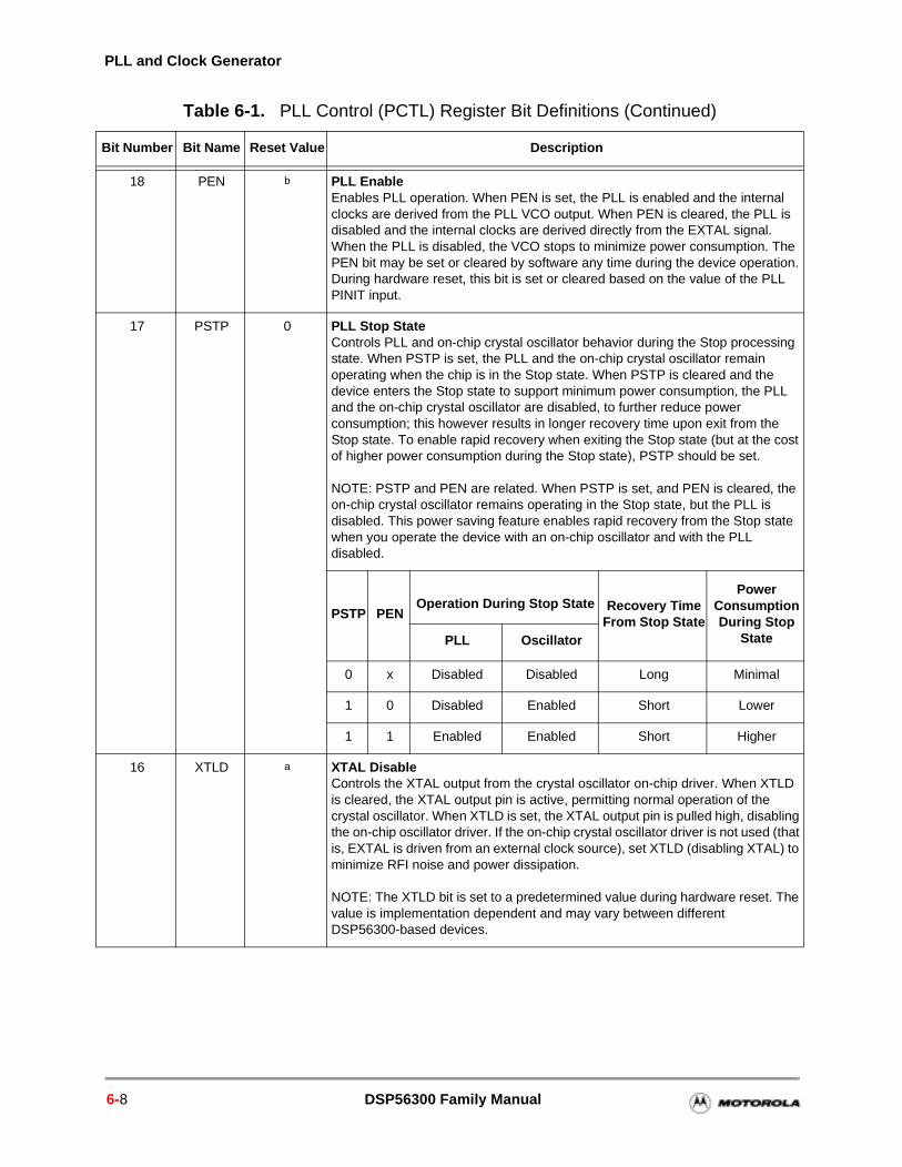
PLL and Clock Generator
18 PEN b PLL EnableEnables PLL operation. When PEN is set, the PLL is enabled and the internal clocks are derived from the PLL VCO output. When PEN is cleared, the PLL is disabled and the internal clocks are derived directly from the EXTAL signal. When the PLL is disabled, the VCO stops to minimize power consumption. The PEN bit may be set or cleared by software any time during the device operation. During hardware reset, this bit is set or cleared based on the value of the PLL PINIT input.
17 PSTP 0 PLL Stop State Controls PLL and on-chip crystal oscillator behavior during the Stop processing state. When PSTP is set, the PLL and the on-chip crystal oscillator remain operating when the chip is in the Stop state. When PSTP is cleared and the device enters the Stop state to support minimum power consumption, the PLL and the on-chip crystal oscillator are disabled, to further reduce power consumption; this however results in longer recovery time upon exit from the Stop state. To enable rapid recovery when exiting the Stop state (but at the cost of higher power consumption during the Stop state), PSTP should be set.
NOTE: PSTP and PEN are related. When PSTP is set, and PEN is cleared, the on-chip crystal oscillator remains operating in the Stop state, but the PLL is disabled. This power saving feature enables rapid recovery from the Stop state when you operate the device with an on-chip oscillator and with the PLL disabled.
PSTP PENOperation During Stop State Recovery Time
From Stop State
Power ConsumptionDuring Stop
StatePLL Oscillator
0 x Disabled Disabled Long Minimal
1 0 Disabled Enabled Short Lower
1 1 Enabled Enabled Short Higher
16 XTLD a XTAL DisableControls the XTAL output from the crystal oscillator on-chip driver. When XTLD is cleared, the XTAL output pin is active, permitting normal operation of the crystal oscillator. When XTLD is set, the XTAL output pin is pulled high, disabling the on-chip oscillator driver. If the on-chip crystal oscillator driver is not used (that is, EXTAL is driven from an external clock source), set XTLD (disabling XTAL) to minimize RFI noise and power dissipation.
NOTE: The XTLD bit is set to a predetermined value during hardware reset. The value is implementation dependent and may vary between different DSP56300-based devices.
Table 6-1. PLL Control (PCTL) Register Bit Definitions (Continued)
Bit Number Bit Name Reset Value Description
6-8 DSP56300 Family Manual
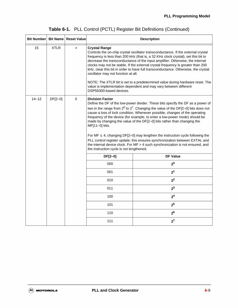
PLL Programming Model
15 XTLR a Crystal RangeControls the on-chip crystal oscillator transconductance. If the external crystalfrequency is less than 200 kHz (that is, a 32 KHz clock crystal), set this bit to decrease the transconductance of the input amplifier. Otherwise, the internal clocks may not be stable. If the external crystal frequency is greater than 200 kHz, clear this bit in order to have full transconductance. Otherwise, the crystal oscillator may not function at all.
NOTE: The XTLR bit is set to a predetermined value during hardware reset. The value is implementation dependent and may vary between different DSP56300-based devices.
14–12 DF[2–0] 0 Division FactorDefine the DF of the low-power divider. These bits specify the DF as a power of
two in the range from 20 to 27. Changing the value of the DF[2–0] bits does not cause a loss of lock condition. Whenever possible, changes of the operating frequency of the device (for example, to enter a low-power mode) should be made by changing the value of the DF[2–0] bits rather than changing the MF[11–0] bits.
For MF ≤ 4, changing DF[2–0] may lengthen the instruction cycle following the PLL control register update; this ensures synchronization between EXTAL and the internal device clock. For MF > 4 such synchronization is not ensured, and the instruction cycle is not lengthened.
DF[2–0] DF Value
000 20
001 21
010 22
011 23
100 24
101 25
110 26
111 27
Table 6-1. PLL Control (PCTL) Register Bit Definitions (Continued)
Bit Number Bit Name Reset Value Description
PLL and Clock Generator 6-9
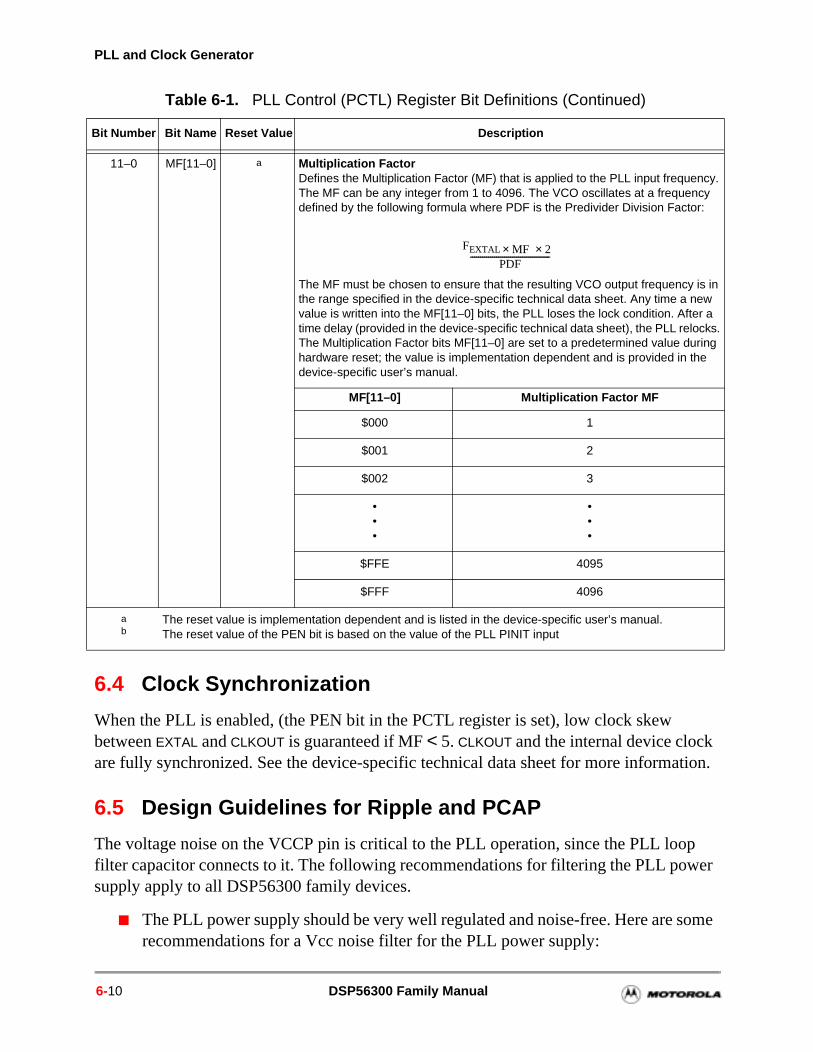
PLL and Clock Generator
6.4 Clock Synchronization
When the PLL is enabled, (the PEN bit in the PCTL register is set), low clock skew between EXTAL and CLKOUT is guaranteed if MF < 5. CLKOUT and the internal device clock are fully synchronized. See the device-specific technical data sheet for more information.
6.5 Design Guidelines for Ripple and PCAP
The voltage noise on the VCCP pin is critical to the PLL operation, since the PLL loop filter capacitor connects to it. The following recommendations for filtering the PLL power supply apply to all DSP56300 family devices.
The PLL power supply should be very well regulated and noise-free. Here are some recommendations for a Vcc noise filter for the PLL power supply:
11–0 MF[11–0] a Multiplication FactorDefines the Multiplication Factor (MF) that is applied to the PLL input frequency. The MF can be any integer from 1 to 4096. The VCO oscillates at a frequency defined by the following formula where PDF is the Predivider Division Factor:
The MF must be chosen to ensure that the resulting VCO output frequency is in the range specified in the device-specific technical data sheet. Any time a new value is written into the MF[11–0] bits, the PLL loses the lock condition. After a time delay (provided in the device-specific technical data sheet), the PLL relocks. The Multiplication Factor bits MF[11–0] are set to a predetermined value during hardware reset; the value is implementation dependent and is provided in the device-specific user’s manual.
MF[11–0] Multiplication Factor MF
$000 1
$001 2
$002 3
•••
•••
$FFE 4095
$FFF 4096
ab
The reset value is implementation dependent and is listed in the device-specific user’s manual.The reset value of the PEN bit is based on the value of the PLL PINIT input
Table 6-1. PLL Control (PCTL) Register Bit Definitions (Continued)
Bit Number Bit Name Reset Value Description
Fextal MF × 2×PDF
----------------------------------------FEXTAL
6-10 DSP56300 Family Manual
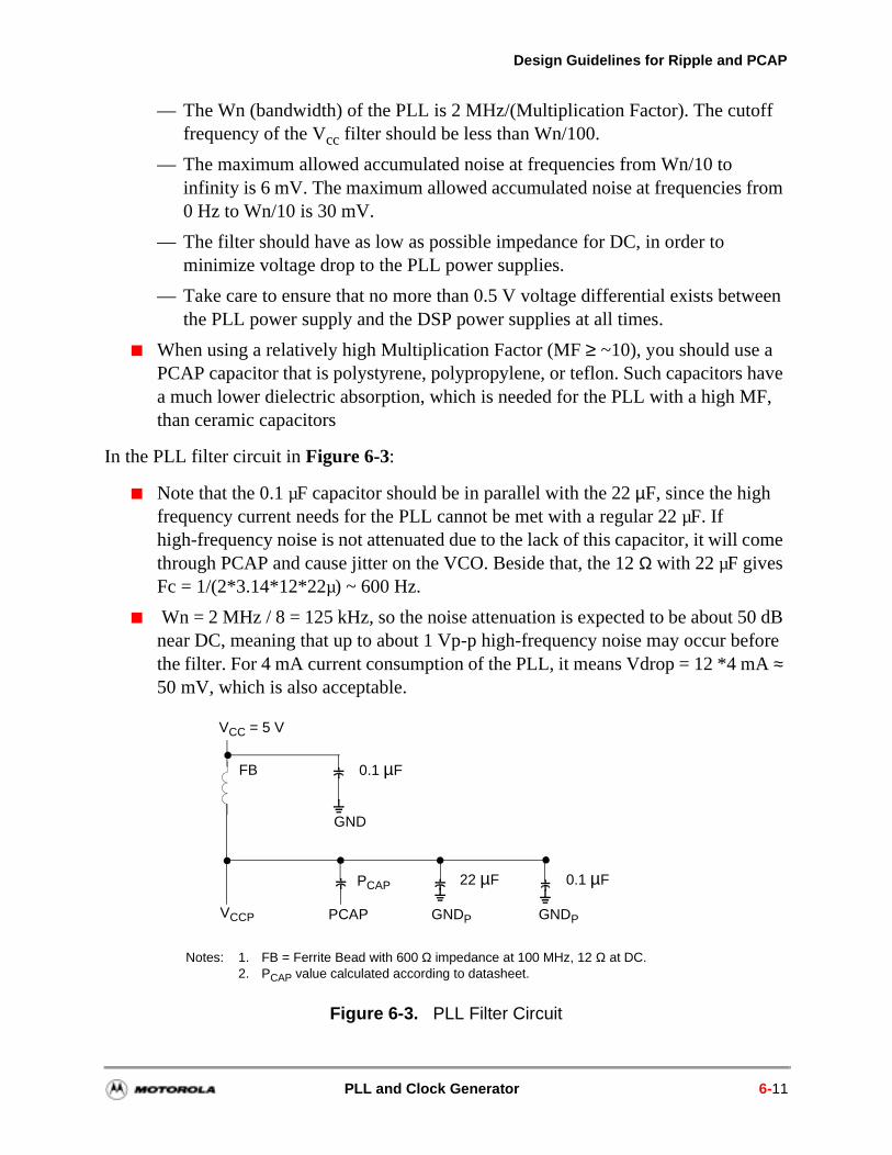
Design Guidelines for Ripple and PCAP
om
een
have F,
— The Wn (bandwidth) of the PLL is 2 MHz/(Multiplication Factor). The cutofffrequency of the Vcc filter should be less than Wn/100.
— The maximum allowed accumulated noise at frequencies from Wn/10 to infinity is 6 mV. The maximum allowed accumulated noise at frequencies fr0 Hz to Wn/10 is 30 mV.
— The filter should have as low as possible impedance for DC, in order to minimize voltage drop to the PLL power supplies.
— Take care to ensure that no more than 0.5 V voltage differential exists betwthe PLL power supply and the DSP power supplies at all times.
When using a relatively high Multiplication Factor (MF ≥ ~10), you should use a PCAP capacitor that is polystyrene, polypropylene, or teflon. Such capacitors a much lower dielectric absorption, which is needed for the PLL with a high Mthan ceramic capacitors
In the PLL filter circuit in Figure 6-3:
Note that the 0.1 µF capacitor should be in parallel with the 22 µF, since the high frequency current needs for the PLL cannot be met with a regular 22 µF. If high-frequency noise is not attenuated due to the lack of this capacitor, it will come through PCAP and cause jitter on the VCO. Beside that, the 12 Ω with 22 µF gives Fc = 1/(2*3.14*12*22µ) ~ 600 Hz.
Wn = 2 MHz / 8 = 125 kHz, so the noise attenuation is expected to be about 50 dB near DC, meaning that up to about 1 Vp-p high-frequency noise may occur before the filter. For 4 mA current consumption of the PLL, it means Vdrop = 12 *4 mA ≈ 50 mV, which is also acceptable.
Figure 6-3. PLL Filter Circuit
VCC = 5 V
GND
0.1 µF
PCAP 22 µF 0.1 µF
VCCP PCAP GNDPGNDP
FB
Notes: 1. FB = Ferrite Bead with 600 Ω impedance at 100 MHz, 12 Ω at DC.2. PCAP value calculated according to datasheet.
PLL and Clock Generator 6-11

PLL and Clock Generator
6-12 DSP56300 Family Manual
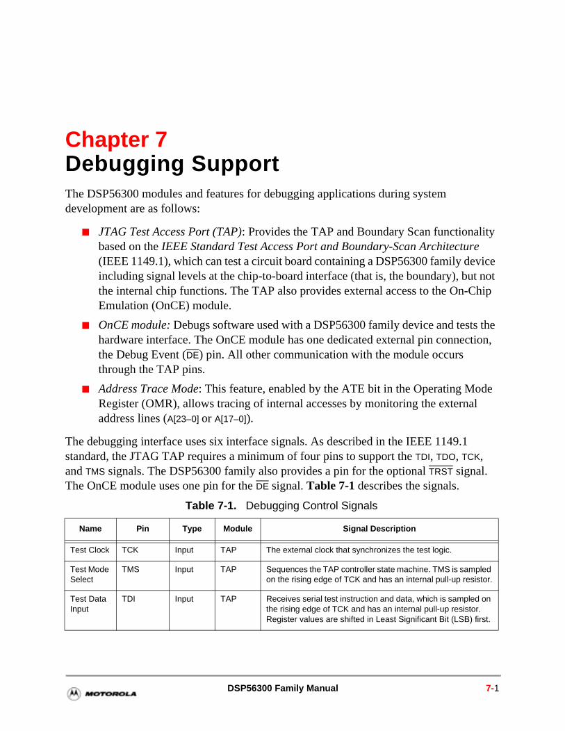
Chapter 7Debugging SupportThe DSP56300 modules and features for debugging applications during system development are as follows:
JTAG Test Access Port (TAP): Provides the TAP and Boundary Scan functionality based on the IEEE Standard Test Access Port and Boundary-Scan Architecture (IEEE 1149.1), which can test a circuit board containing a DSP56300 family device including signal levels at the chip-to-board interface (that is, the boundary), but not the internal chip functions. The TAP also provides external access to the On-Chip Emulation (OnCE) module.
OnCE module: Debugs software used with a DSP56300 family device and tests the hardware interface. The OnCE module has one dedicated external pin connection, the Debug Event (DE) pin. All other communication with the module occurs through the TAP pins.
Address Trace Mode: This feature, enabled by the ATE bit in the Operating Mode Register (OMR), allows tracing of internal accesses by monitoring the external address lines (A[23–0] or A[17–0]).
The debugging interface uses six interface signals. As described in the IEEE 1149.1 standard, the JTAG TAP requires a minimum of four pins to support the TDI, TDO, TCK, and TMS signals. The DSP56300 family also provides a pin for the optional TRST signal. The OnCE module uses one pin for the DE signal. Table 7-1 describes the signals.
Table 7-1. Debugging Control Signals
Name Pin Type Module Signal Description
Test Clock TCK Input TAP The external clock that synchronizes the test logic.
Test Mode Select
TMS Input TAP Sequences the TAP controller state machine. TMS is sampled on the rising edge of TCK and has an internal pull-up resistor.
Test Data Input
TDI Input TAP Receives serial test instruction and data, which is sampled on the rising edge of TCK and has an internal pull-up resistor. Register values are shifted in Least Significant Bit (LSB) first.
DSP56300 Family Manual 7-1
Debugging Support
7.1 JTAG Test Access Port
The DSP56300 core provides a dedicated user-accessible Test Access Port (TAP) based on the IEEE Standard Test Access Port and Boundary-Scan Architecture (IEEE 1149.1). Problems of testing high density circuit boards led to development of this standard under the sponsorship of the Test Technology Committee of IEEE and the Joint Test Action Group (JTAG). The DSP56300 core implementation supports circuit-board test strategies based on this standard.
7.1.1 Boundary Scan Architecture Overview
The test logic includes a TAP consisting of four dedicated signal pins, a 16-state controller, and three test data registers. A Boundary Scan Register (BSR) links all device signal pins into a single shift register. The test logic, implemented with static logic design,
Test Data Output
TDO Output TAP The serial output for test instructions and data. TDO is tri-stateable and is actively driven in the shift-IR and shift-DR controller states. TDO changes on the falling edge of TCK. Register values are shifted out LSB first.
Test Reset TRST Input TAP Initializes the test controller asynchronously. TRST has an internal pull-up resistor. To reset the TAP controller synchronously, use TCK to clock five consecutive 1s into TMS. To reset the remaining parts of the DSP core and the peripherals (or in some cases, such as the HI32, only the internal portion of a peripheral), use the RESET input signal.
Debug Event
DE Input or Output
OnCE An open-drain signal providing, as an input, a means of entering the Debug mode of operation from an external command controller, and, as an output, a means of acknowledging that the chip has entered the Debug mode. This signal, when asserted as an input, causes the DSP56300 core to finish executing the current instruction, save the instruction pipeline information, enter Debug mode, and wait for commands to be entered from the debug serial input line. This signal is asserted as an output for three clock cycles when the chip enters Debug mode as a result of a debug request or as a result of meeting a breakpoint condition. The DE has an internal pull-up resistor.
This is not a standard part of the JTAG Test Access Port (TAP) Controller. The signal connects directly to the OnCE module to initiate Debug mode directly or to provide a direct external indication that the chip has entered Debug mode. All other interaction with the OnCE module must occur through the JTAG port.
Table 7-1. Debugging Control Signals (Continued)
Name Pin Type Module Signal Description
7-2 DSP56300 Family Manual
JTAG Test Access Port
is independent of the device system logic. The DSP56300 core has the following capabilities initiated by the associated JTAG commands (listed in parentheses):
Perform boundary scan operations to test circuit-board electrical continuity (EXTEST)
Bypass the DSP56300 core for a given circuit board test by effectively reducing the BSR to a single cell (BYPASS)
Sample the DSP56300 core-based device system pins during operation and transparently shift out the result in the BSR; preload values to output pins prior to invoking the EXTEST instruction (SAMPLE/PRELOAD)
Disable the output drive to pins during circuit-board testing (HI-Z)
Access the OnCE controller and circuits to control a target system (ENABLE_ONCE)
Enter the Debug mode of operation (DEBUG_REQUEST)
Query identification information on manufacturer, part number, and version from a DSP56300 core-based device (IDCODE)
Force test data onto the outputs of a DSP56300 core-based device while replacing its BSR in the serial data path with a single-bit register (CLAMP)
This section discusses aspects of the JTAG implementation that are specific to the DSP56300 core and is to be used with the supporting IEEE 1149.1 standards document. The discussion covers items the standard requires to be defined and includes additional information specific to the DSP56300 core implementation. Figure 7-1 shows the block diagram of the DSP56300 core implementation of JTAG, which includes a 4-bit Instruction Register and three test registers: a 1-bit Bypass Register, a 32-bit Identification Register, and a Boundary Scan Register (BSR) whose size is chip-specific. This implementation includes a dedicated TAP and five pins.
7.1.2 TAP Controller
The TAP controller interprets the sequence of logical values on the TMS signal. It is a synchronous state machine that controls the operation of the JTAG logic. Figure 7-2 shows the state machine. The value shown adjacent to each change-of-state arrow represents the value of the TMS signal sampled on the rising edge of the TCK signal. For a description of the TAP controller states, see the IEEE 1149.1 specification.
Debugging Support 7-3
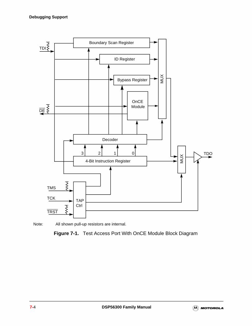
Debugging Support
Figure 7-1. Test Access Port With OnCE Module Block Diagram
Boundary Scan Register
MU
X4-Bit Instruction Register
TDO
TAPCtrl
TDI
TMS
TCK
023 1
OnCE
ID Register
TRST
Decoder
MU
X
Bypass Register
ModuleDE
Note: All shown pull-up resistors are internal.
7-4 DSP56300 Family Manual
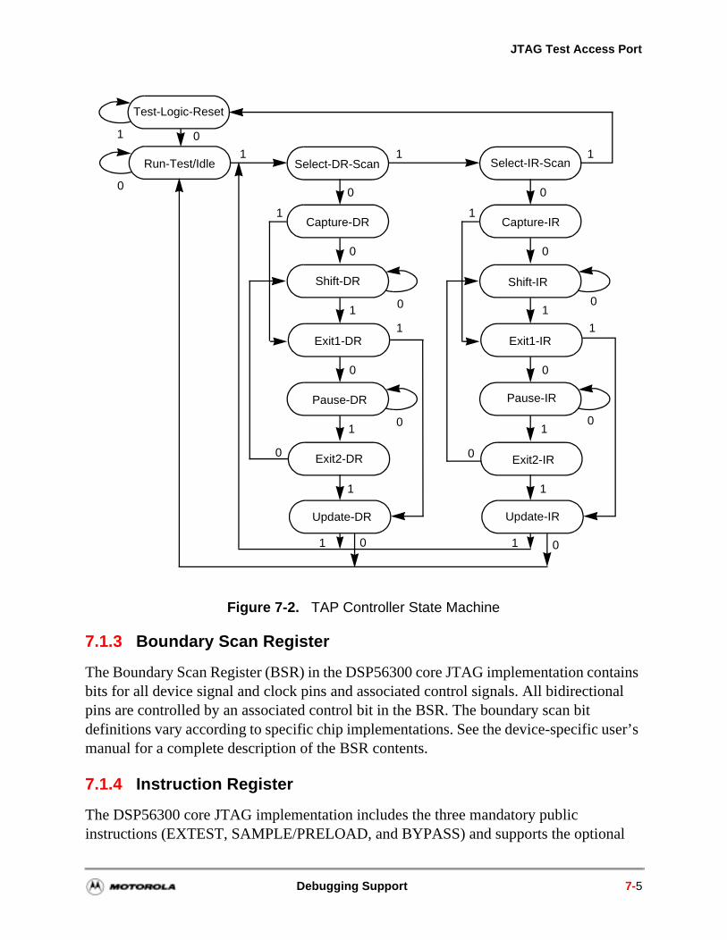
JTAG Test Access Port
ser’s
al
Figure 7-2. TAP Controller State Machine
7.1.3 Boundary Scan Register
The Boundary Scan Register (BSR) in the DSP56300 core JTAG implementation contains bits for all device signal and clock pins and associated control signals. All bidirectional pins are controlled by an associated control bit in the BSR. The boundary scan bit definitions vary according to specific chip implementations. See the device-specific umanual for a complete description of the BSR contents.
7.1.4 Instruction Register
The DSP56300 core JTAG implementation includes the three mandatory public instructions (EXTEST, SAMPLE/PRELOAD, and BYPASS) and supports the option
Select-DR-Scan
Capture-DR
Shift-DR
Exit1-DR
Pause-DR
Exit2-DR
Test-Logic-Reset
Run-Test/Idle
Update-DR
1
0
0
1
0
1
1
0
1
1
0
0
1 0
Select-IR-Scan
Capture-IR
Shift-IR
Exit1-IR
Pause-IR
Exit2-IR
Update-IR
0
0
1
0
1
1
0
1
1
0
0
1 0
01
0
1 1
Debugging Support 7-5
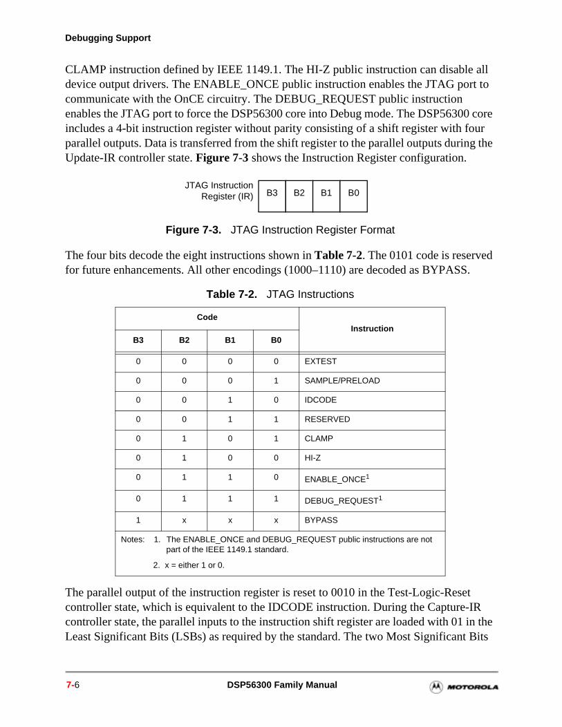
Debugging Support
.
t R n the Bits
CLAMP instruction defined by IEEE 1149.1. The HI-Z public instruction can disable all device output drivers. The ENABLE_ONCE public instruction enables the JTAG port to communicate with the OnCE circuitry. The DEBUG_REQUEST public instruction enables the JTAG port to force the DSP56300 core into Debug mode. The DSP56300 core includes a 4-bit instruction register without parity consisting of a shift register with four parallel outputs. Data is transferred from the shift register to the parallel outputs during the Update-IR controller state. Figure 7-3 shows the Instruction Register configuration.
The four bits decode the eight instructions shown in Table 7-2. The 0101 code is reserved for future enhancements. All other encodings (1000–1110) are decoded as BYPASS
The parallel output of the instruction register is reset to 0010 in the Test-Logic-Resecontroller state, which is equivalent to the IDCODE instruction. During the Capture-Icontroller state, the parallel inputs to the instruction shift register are loaded with 01 iLeast Significant Bits (LSBs) as required by the standard. The two Most Significant
Figure 7-3. JTAG Instruction Register Format
Table 7-2. JTAG Instructions
CodeInstruction
B3 B2 B1 B0
0 0 0 0 EXTEST
0 0 0 1 SAMPLE/PRELOAD
0 0 1 0 IDCODE
0 0 1 1 RESERVED
0 1 0 1 CLAMP
0 1 0 0 HI-Z
0 1 1 0 ENABLE_ONCE1
0 1 1 1 DEBUG_REQUEST1
1 x x x BYPASS
Notes: 1. The ENABLE_ONCE and DEBUG_REQUEST public instructions are not part of the IEEE 1149.1 standard.
2. x = either 1 or 0.
JTAG InstructionRegister (IR) B3 B2 B1 B0
7-6 DSP56300 Family Manual
JTAG Test Access Port
(MSBs) are loaded with the values of the core status bits OS1 and OS0 from the OnCE controller.
7.1.4.1 EXTEST (B[3–0] = 0000)
The external test (EXTEST) instruction selects the BSR. The EXTEST instruction also asserts internal reset for the DSP56300 core system logic to force a predictable internal state while performing external boundary scan operations. Using the TAP, the BSR can:
Scan user-defined values into the output buffers
Capture values presented to input pins
Control the direction of bidirectional pins
Control the output drive of tri-stateable output pins
For details on the function and use of EXTEST, refer to the IEEE 1149.1 standards document.
7.1.4.2 SAMPLE/PRELOAD (B[3–0] = 0001)
The SAMPLE/PRELOAD instruction performs two separate functions. First, it obtains a snapshot of system data and control signals that occurs on the rising edge of TCK in the Capture-DR controller state. The data is observed by shifting it transparently through the BSR.
Note: Since no internal synchronization exists between the JTAG clock (TCK) and the system clock (CLK), you must provide some form of external synchronization to achieve meaningful results.
Secondly, SAMPLE/PRELOAD can initialize the BSR output cells prior to selection of EXTEST. This initialization ensures that known data appears on the outputs when the EXTEST instruction starts executing.
7.1.4.3 IDCODE (B[3–0] = 0010)
The IDCODE instruction selects the ID register. This public instruction allows identification of the manufacturer, part number, and version of a component through the TAP. Figure 7-4 shows the ID register configuration.
Debugging Support 7-7
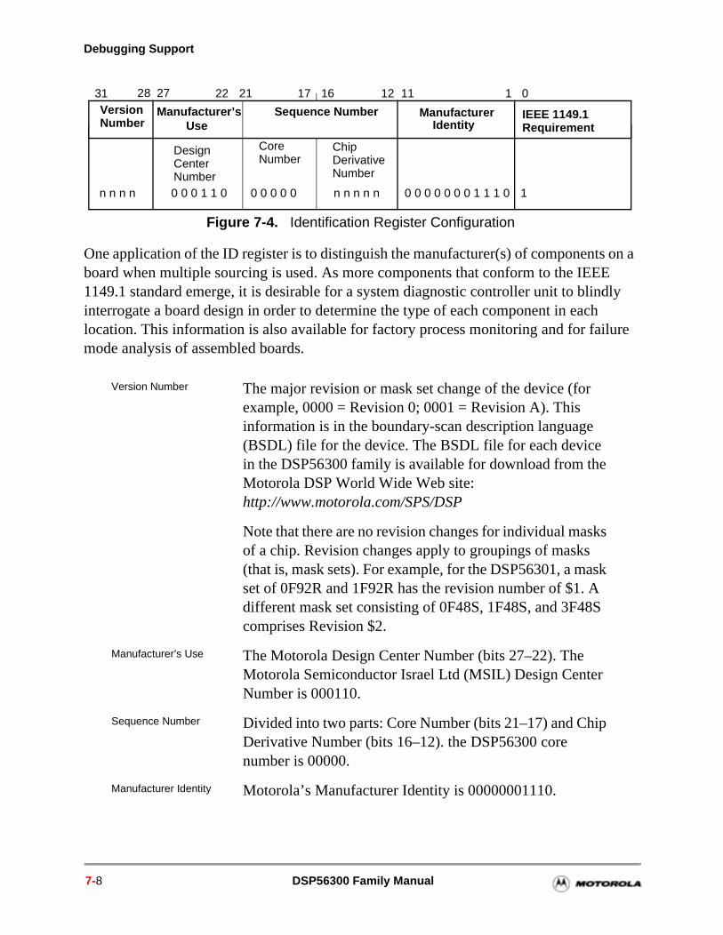
Debugging Support
Figure 7-4. Identification Register Configuration
One application of the ID register is to distinguish the manufacturer(s) of components on a board when multiple sourcing is used. As more components that conform to the IEEE 1149.1 standard emerge, it is desirable for a system diagnostic controller unit to blindly interrogate a board design in order to determine the type of each component in each location. This information is also available for factory process monitoring and for failure mode analysis of assembled boards.
Version Number The major revision or mask set change of the device (for example, 0000 = Revision 0; 0001 = Revision A). This information is in the boundary-scan description language (BSDL) file for the device. The BSDL file for each device in the DSP56300 family is available for download from the Motorola DSP World Wide Web site: http://www.motorola.com/SPS/DSP
Note that there are no revision changes for individual masks of a chip. Revision changes apply to groupings of masks (that is, mask sets). For example, for the DSP56301, a mask set of 0F92R and 1F92R has the revision number of $1. A different mask set consisting of 0F48S, 1F48S, and 3F48S comprises Revision $2.
Manufacturer’s Use The Motorola Design Center Number (bits 27–22). The Motorola Semiconductor Israel Ltd (MSIL) Design Center Number is 000110.
Sequence Number Divided into two parts: Core Number (bits 21–17) and Chip Derivative Number (bits 16–12). the DSP56300 core number is 00000.
Manufacturer Identity Motorola’s Manufacturer Identity is 00000001110.
01111231
n n n n 10 0 0 0 0 0 0 1 1 1 0
2122 1617
0 0 0 0 0 0 0 0 1 1 0 n n n n n
IEEE 1149.1Requirement
ManufacturerIdentity
DesignCenterNumber
2728
Manufacturer’sUse
CoreNumber
ChipDerivativeNumber
VersionNumber
Sequence Number
7-8 DSP56300 Family Manual
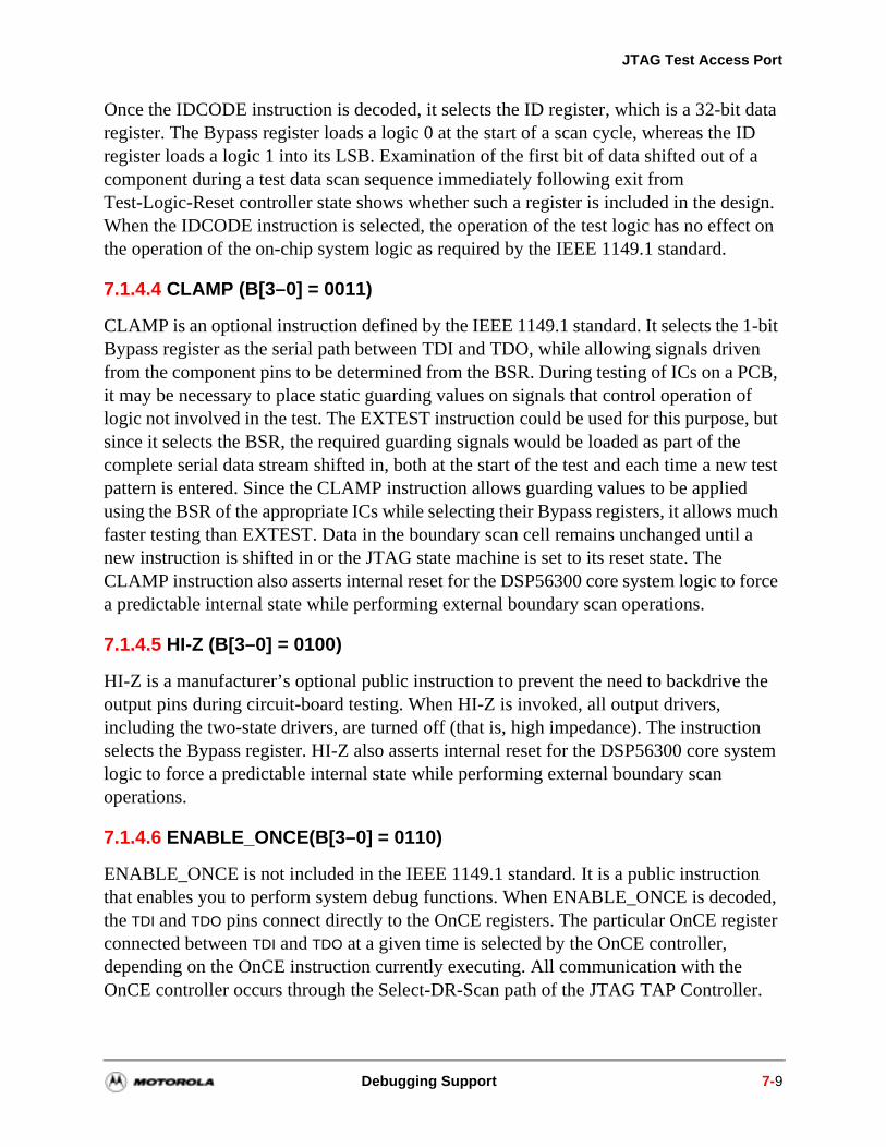
JTAG Test Access Port
the
on system
Once the IDCODE instruction is decoded, it selects the ID register, which is a 32-bit data register. The Bypass register loads a logic 0 at the start of a scan cycle, whereas the ID register loads a logic 1 into its LSB. Examination of the first bit of data shifted out of a component during a test data scan sequence immediately following exit from Test-Logic-Reset controller state shows whether such a register is included in the design. When the IDCODE instruction is selected, the operation of the test logic has no effect on the operation of the on-chip system logic as required by the IEEE 1149.1 standard.
7.1.4.4 CLAMP (B[3–0] = 0011)
CLAMP is an optional instruction defined by the IEEE 1149.1 standard. It selects the 1-bit Bypass register as the serial path between TDI and TDO, while allowing signals driven from the component pins to be determined from the BSR. During testing of ICs on a PCB, it may be necessary to place static guarding values on signals that control operation of logic not involved in the test. The EXTEST instruction could be used for this purpose, but since it selects the BSR, the required guarding signals would be loaded as part of the complete serial data stream shifted in, both at the start of the test and each time a new test pattern is entered. Since the CLAMP instruction allows guarding values to be applied using the BSR of the appropriate ICs while selecting their Bypass registers, it allows much faster testing than EXTEST. Data in the boundary scan cell remains unchanged until a new instruction is shifted in or the JTAG state machine is set to its reset state. The CLAMP instruction also asserts internal reset for the DSP56300 core system logic to force a predictable internal state while performing external boundary scan operations.
7.1.4.5 HI-Z (B[3–0] = 0100)
HI-Z is a manufacturer’s optional public instruction to prevent the need to backdrive output pins during circuit-board testing. When HI-Z is invoked, all output drivers, including the two-state drivers, are turned off (that is, high impedance). The instructiselects the Bypass register. HI-Z also asserts internal reset for the DSP56300 core logic to force a predictable internal state while performing external boundary scan operations.
7.1.4.6 ENABLE_ONCE(B[3–0] = 0110)
ENABLE_ONCE is not included in the IEEE 1149.1 standard. It is a public instruction that enables you to perform system debug functions. When ENABLE_ONCE is decoded, the TDI and TDO pins connect directly to the OnCE registers. The particular OnCE register connected between TDI and TDO at a given time is selected by the OnCE controller, depending on the OnCE instruction currently executing. All communication with the OnCE controller occurs through the Select-DR-Scan path of the JTAG TAP Controller.
Debugging Support 7-9
Debugging Support
e the
7.1.4.7 DEBUG_REQUEST(B[3–0] = 0111)
DEBUG_REQUEST is not included in the IEEE 1149.1 standard. It is a public instruction that enables you to generate a debug request signal to the DSP56300 core. When DEBUG_REQUEST is decoded, the TDI and TDO pins connect to the instruction registers. In the Capture-IR state of the TAP, the OnCE status bits are captured in the Instruction shift register, so the external JTAG controller must continue to shift in the DEBUG_REQUEST while polling the status bits that are shifted out until the Debug mode of operation is entered (acknowledged by the combination 11 on OS[1–0]). After acknowledgment of Debug mode is received, the external JTAG controller must issuENABLE_ONCE instruction so you can perform system debug functions.
7.1.4.8 BYPASS (B[3–0] = 1111)
BYPASS selects the single-bit Bypass register, as shown in Figure 7-5. This creates a shift-register path from TDI to the Bypass register, and finally to TDO, circumventing the BSR. This instruction enhances test efficiency when a component other than the DSP56300 core-based device becomes the device under test. When the current instruction selects the Bypass register, the shift-register stage is set to a logic 0 on the rising edge of TCK in the Capture-DR controller state. Therefore, the first bit shifted out after selection of the Bypass register is always a logic 0.
7.1.5 DSP56300 JTAG Restrictions
The control afforded by the output enable signals using the BSR and the EXTEST instruction requires a compatible circuit-board test environment to avoid device-destructive configurations. You must avoid situations in which the DSP56300 core output drivers are enabled into actively driven networks. In addition, EXTEST can execute only after power-up or regular hardware reset while EXTAL is provided. While EXTEST executes, EXTAL can remain inactive.
Two constraints relate to the JTAG interface. First, the TCK input does not include an internal pull-up resistor and should not be left unconnected. The second constraint is to ensure that the JTAG test logic is kept transparent to the system logic by forcing the TAP
Figure 7-5. Bypass Register
1
1Mux
G1
CD
To TDOFrom TDI
0
Shift DR
CLOCKDR
7-10 DSP56300 Family Manual
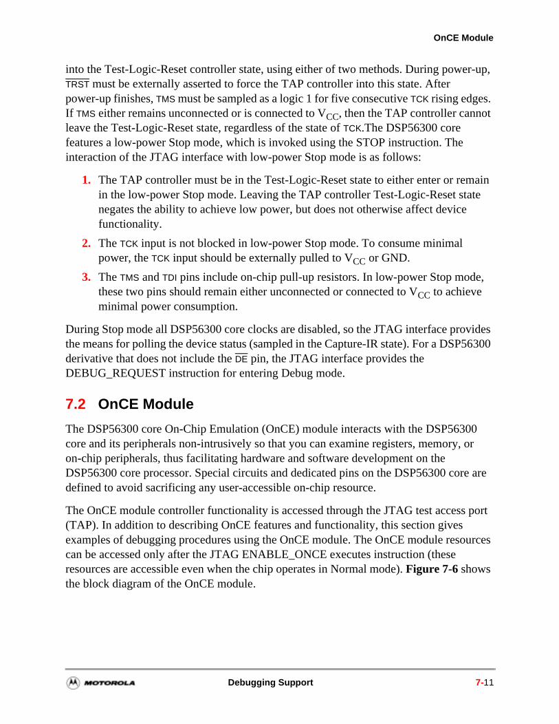
OnCE Module
into the Test-Logic-Reset controller state, using either of two methods. During power-up, TRST must be externally asserted to force the TAP controller into this state. After power-up finishes, TMS must be sampled as a logic 1 for five consecutive TCK rising edges. If TMS either remains unconnected or is connected to VCC, then the TAP controller cannot leave the Test-Logic-Reset state, regardless of the state of TCK.The DSP56300 core features a low-power Stop mode, which is invoked using the STOP instruction. The interaction of the JTAG interface with low-power Stop mode is as follows:
1. The TAP controller must be in the Test-Logic-Reset state to either enter or remain in the low-power Stop mode. Leaving the TAP controller Test-Logic-Reset state negates the ability to achieve low power, but does not otherwise affect device functionality.
2. The TCK input is not blocked in low-power Stop mode. To consume minimal power, the TCK input should be externally pulled to VCC or GND.
3. The TMS and TDI pins include on-chip pull-up resistors. In low-power Stop mode, these two pins should remain either unconnected or connected to VCC to achieve minimal power consumption.
During Stop mode all DSP56300 core clocks are disabled, so the JTAG interface provides the means for polling the device status (sampled in the Capture-IR state). For a DSP56300 derivative that does not include the DE pin, the JTAG interface provides the DEBUG_REQUEST instruction for entering Debug mode.
7.2 OnCE Module
The DSP56300 core On-Chip Emulation (OnCE) module interacts with the DSP56300 core and its peripherals non-intrusively so that you can examine registers, memory, or on-chip peripherals, thus facilitating hardware and software development on the DSP56300 core processor. Special circuits and dedicated pins on the DSP56300 core are defined to avoid sacrificing any user-accessible on-chip resource.
The OnCE module controller functionality is accessed through the JTAG test access port (TAP). In addition to describing OnCE features and functionality, this section gives examples of debugging procedures using the OnCE module. The OnCE module resources can be accessed only after the JTAG ENABLE_ONCE executes instruction (these resources are accessible even when the chip operates in Normal mode). Figure 7-6 shows the block diagram of the OnCE module.
Debugging Support 7-11
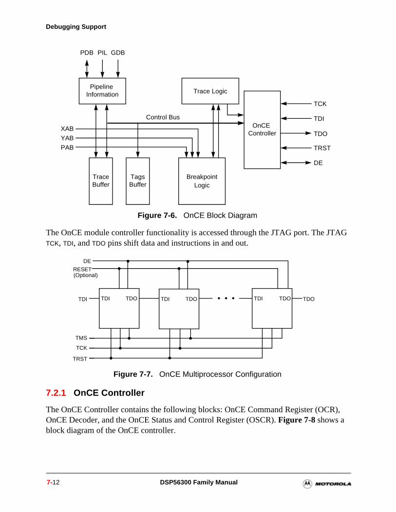
Debugging Support
Figure 7-6. OnCE Block Diagram
The OnCE module controller functionality is accessed through the JTAG port. The JTAG TCK, TDI, and TDO pins shift data and instructions in and out.
Figure 7-7. OnCE Multiprocessor Configuration
7.2.1 OnCE Controller
The OnCE Controller contains the following blocks: OnCE Command Register (OCR), OnCE Decoder, and the OnCE Status and Control Register (OSCR). Figure 7-8 shows a block diagram of the OnCE controller.
TraceBuffer
BreakpointLogic
Pipeline Information Trace Logic
OnCE Controller
PAB
YAB
XAB
PDB PIL GDB
TDO
TRST
TDI
TCK
TagsBuffer
Control Bus
DE
TDI TDO TDI TDOTDI TDOTDI
TMS
TCK
DE
TDO
TRST
RESET(Optional)
7-12 DSP56300 Family Manual
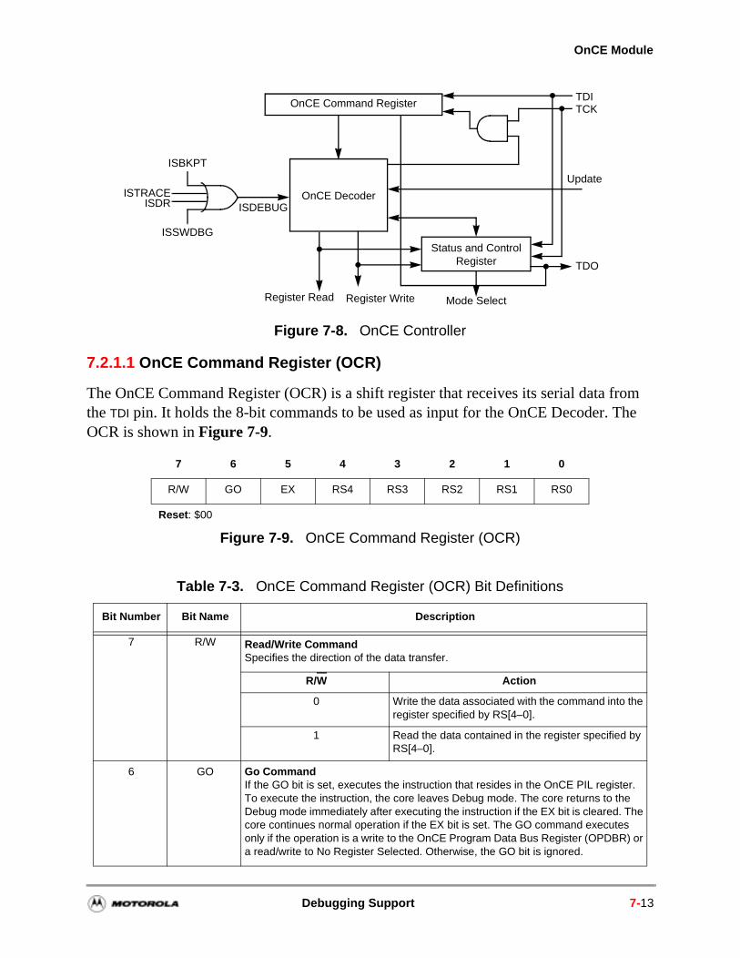
OnCE Module
Figure 7-8. OnCE Controller
7.2.1.1 OnCE Command Register (OCR)
The OnCE Command Register (OCR) is a shift register that receives its serial data from the TDI pin. It holds the 8-bit commands to be used as input for the OnCE Decoder. The OCR is shown in Figure 7-9.
7 6 5 4 3 2 1 0
R/W GO EX RS4 RS3 RS2 RS1 RS0
Reset: $00
Figure 7-9. OnCE Command Register (OCR)
Table 7-3. OnCE Command Register (OCR) Bit Definitions
Bit Number Bit Name Description
7 R/W Read/Write CommandSpecifies the direction of the data transfer.
R/W Action
0 Write the data associated with the command into the register specified by RS[4–0].
1 Read the data contained in the register specified by RS[4–0].
6 GO Go CommandIf the GO bit is set, executes the instruction that resides in the OnCE PIL register. To execute the instruction, the core leaves Debug mode. The core returns to the Debug mode immediately after executing the instruction if the EX bit is cleared. The core continues normal operation if the EX bit is set. The GO command executes only if the operation is a write to the OnCE Program Data Bus Register (OPDBR) or a read/write to No Register Selected. Otherwise, the GO bit is ignored.
OnCE Command RegisterTDITCK
Status and ControlRegister TDO
Mode Select
OnCE DecoderISDEBUG
ISBKPT
ISSWDBG
ISDRISTRACE
Register WriteRegister Read
Update
Debugging Support 7-13
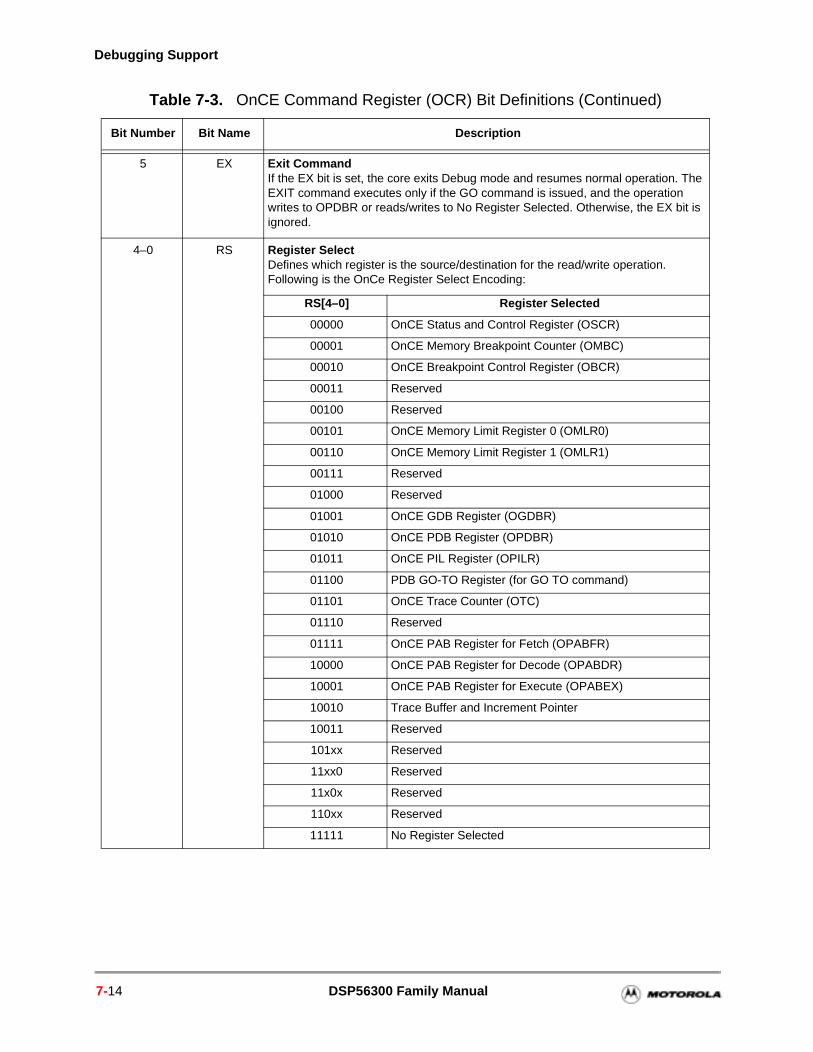
Debugging Support
5 EX Exit CommandIf the EX bit is set, the core exits Debug mode and resumes normal operation. The EXIT command executes only if the GO command is issued, and the operation writes to OPDBR or reads/writes to No Register Selected. Otherwise, the EX bit is ignored.
4–0 RS Register SelectDefines which register is the source/destination for the read/write operation. Following is the OnCe Register Select Encoding:
RS[4–0] Register Selected
00000 OnCE Status and Control Register (OSCR)
00001 OnCE Memory Breakpoint Counter (OMBC)
00010 OnCE Breakpoint Control Register (OBCR)
00011 Reserved
00100 Reserved
00101 OnCE Memory Limit Register 0 (OMLR0)
00110 OnCE Memory Limit Register 1 (OMLR1)
00111 Reserved
01000 Reserved
01001 OnCE GDB Register (OGDBR)
01010 OnCE PDB Register (OPDBR)
01011 OnCE PIL Register (OPILR)
01100 PDB GO-TO Register (for GO TO command)
01101 OnCE Trace Counter (OTC)
01110 Reserved
01111 OnCE PAB Register for Fetch (OPABFR)
10000 OnCE PAB Register for Decode (OPABDR)
10001 OnCE PAB Register for Execute (OPABEX)
10010 Trace Buffer and Increment Pointer
10011 Reserved
101xx Reserved
11xx0 Reserved
11x0x Reserved
110xx Reserved
11111 No Register Selected
Table 7-3. OnCE Command Register (OCR) Bit Definitions (Continued)
Bit Number Bit Name Description
7-14 DSP56300 Family Manual
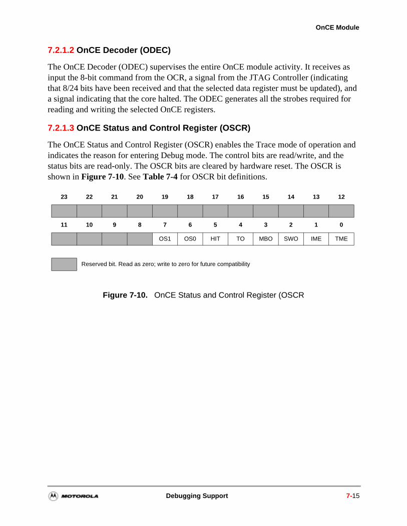
OnCE Module
7.2.1.2 OnCE Decoder (ODEC)
The OnCE Decoder (ODEC) supervises the entire OnCE module activity. It receives as input the 8-bit command from the OCR, a signal from the JTAG Controller (indicating that 8/24 bits have been received and that the selected data register must be updated), and a signal indicating that the core halted. The ODEC generates all the strobes required for reading and writing the selected OnCE registers.
7.2.1.3 OnCE Status and Control Register (OSCR)
The OnCE Status and Control Register (OSCR) enables the Trace mode of operation and indicates the reason for entering Debug mode. The control bits are read/write, and the status bits are read-only. The OSCR bits are cleared by hardware reset. The OSCR is shown in Figure 7-10. See Table 7-4 for OSCR bit definitions.
Figure 7-10. OnCE Status and Control Register (OSCR
23 22 21 20 19 18 17 16 15 14 13 12
11 10 9 8 7 6 5 4 3 2 1 0
OS1 OS0 HIT TO MBO SWO IME TME
Reserved bit. Read as zero; write to zero for future compatibility
Debugging Support 7-15
Debugging Support
Table 7-4. OnCE Status and Control Register (OSCR) Bit Definitions
Bit Number Bit Name Reset Value Description
23–8 0 Reserved. Write to zero for future compatibility.
7–6 OS 0 Core StatusRead-only status bits that provide core status information. Examining the status bits, you can determine whether the chip has entered Debug mode. To find the reason for entering Debug mode, consult the OSCR SWO, MBO, and TO bits. You can also examine these bits to determine why the chip has not entered the Debug mode after debug event assertion (DE) or execution of the JTAG Debug Request instruction (core waiting for the bus, STOP or WAIT instruction, and so on). The OS bits are also reflected in the JTAG instruction shift register, which allows the polling of the core status information at the JTAG level so that you can read the OSCR after the DSP56300 core executes the STOP instruction (and therefore there are no clocks).
OS1 OS0 Description
0 0 DSP56300 core is executing instructions
0 1 DSP56300 core is in Wait or Stop mode
1 0 DSP56300 core is waiting for bus
1 1 DSP56300 core is in Debug mode
5 HIT 0 Cache HitA read-only status bit that is set when a cache hit occurs in Cache mode in the Debug mode of operation. In PRAM mode, this bit reads as one.
4 TO 0 Trace OccurrenceA read-only status bit that is set when all the following occur:
Trace Counter = 0
Trace mode is enabled Debug mode of operation is entered
This bit is cleared when the DSP leaves Debug mode.
3 MBO 0 Memory Breakpoint OccurrenceA read-only status bit that is set when the DSP enters Debug mode because a memory breakpoint has been encountered. This bit is cleared when the DSP leaves Debug mode.
2 SWO 0 Software Debug OccurrenceA read-only status bit that is set when the DSP enters Debug mode because of the execution of the DEBUG or DEBUGcc instruction with condition true. This bit is cleared when the DSP leaves Debug mode.
1 IME 0 Interrupt Mode EnableWhen this control bit is set, the chip executes a vectored interrupt to the address VBA:$06 instead of entering Debug mode.
0 TME 0 Trace Mode EnableWhen set, this control bit enables Trace mode.
7-16 DSP56300 Family Manual
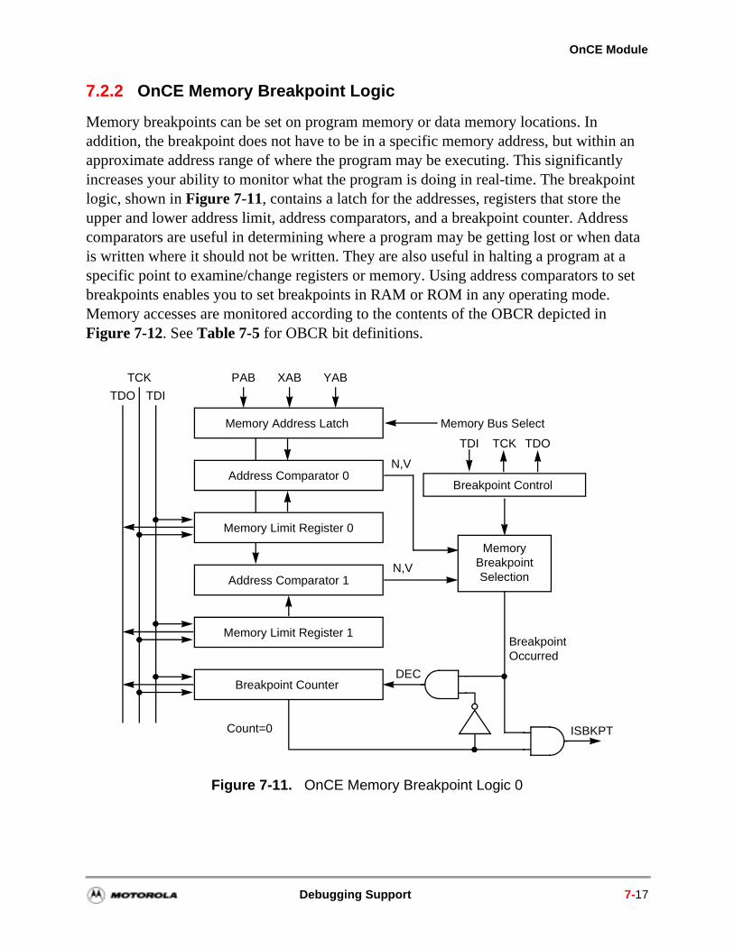
OnCE Module
7.2.2 OnCE Memory Breakpoint Logic
Memory breakpoints can be set on program memory or data memory locations. In addition, the breakpoint does not have to be in a specific memory address, but within an approximate address range of where the program may be executing. This significantly increases your ability to monitor what the program is doing in real-time. The breakpoint logic, shown in Figure 7-11, contains a latch for the addresses, registers that store the upper and lower address limit, address comparators, and a breakpoint counter. Address comparators are useful in determining where a program may be getting lost or when data is written where it should not be written. They are also useful in halting a program at a specific point to examine/change registers or memory. Using address comparators to set breakpoints enables you to set breakpoints in RAM or ROM in any operating mode. Memory accesses are monitored according to the contents of the OBCR depicted in Figure 7-12. See Table 7-5 for OBCR bit definitions.
Figure 7-11. OnCE Memory Breakpoint Logic 0
Memory Address Latch
PAB XAB YAB
Memory Bus Select
Memory Limit Register 1
Address Comparator 1
Memory Limit Register 0
Address Comparator 0
TDITDO
TCK
Breakpoint Counter
MemoryBreakpointSelection
DEC
Breakpoint
Count=0 ISBKPT
Occurred
N,V
N,V
Breakpoint Control
TDI TDOTCK
Debugging Support 7-17
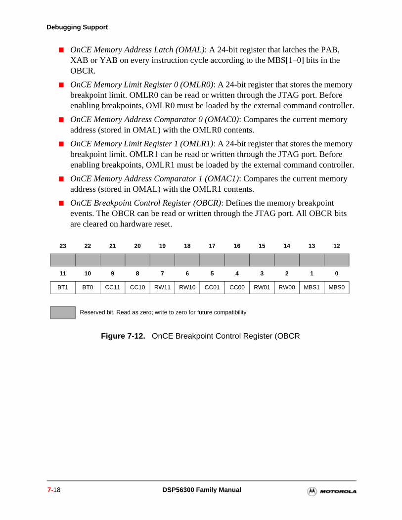
Debugging Support
y oller.
y oller.
its
OnCE Memory Address Latch (OMAL): A 24-bit register that latches the PAB, XAB or YAB on every instruction cycle according to the MBS[1–0] bits in the OBCR.
OnCE Memory Limit Register 0 (OMLR0): A 24-bit register that stores the memorbreakpoint limit. OMLR0 can be read or written through the JTAG port. Beforeenabling breakpoints, OMLR0 must be loaded by the external command contr
OnCE Memory Address Comparator 0 (OMAC0): Compares the current memory address (stored in OMAL) with the OMLR0 contents.
OnCE Memory Limit Register 1 (OMLR1): A 24-bit register that stores the memorbreakpoint limit. OMLR1 can be read or written through the JTAG port. Beforeenabling breakpoints, OMLR1 must be loaded by the external command contr
OnCE Memory Address Comparator 1 (OMAC1): Compares the current memory address (stored in OMAL) with the OMLR1 contents.
OnCE Breakpoint Control Register (OBCR): Defines the memory breakpoint events. The OBCR can be read or written through the JTAG port. All OBCR bare cleared on hardware reset.
Figure 7-12. OnCE Breakpoint Control Register (OBCR
23 22 21 20 19 18 17 16 15 14 13 12
11 10 9 8 7 6 5 4 3 2 1 0
BT1 BT0 CC11 CC10 RW11 RW10 CC01 CC00 RW01 RW00 MBS1 MBS0
Reserved bit. Read as zero; write to zero for future compatibility
7-18 DSP56300 Family Manual
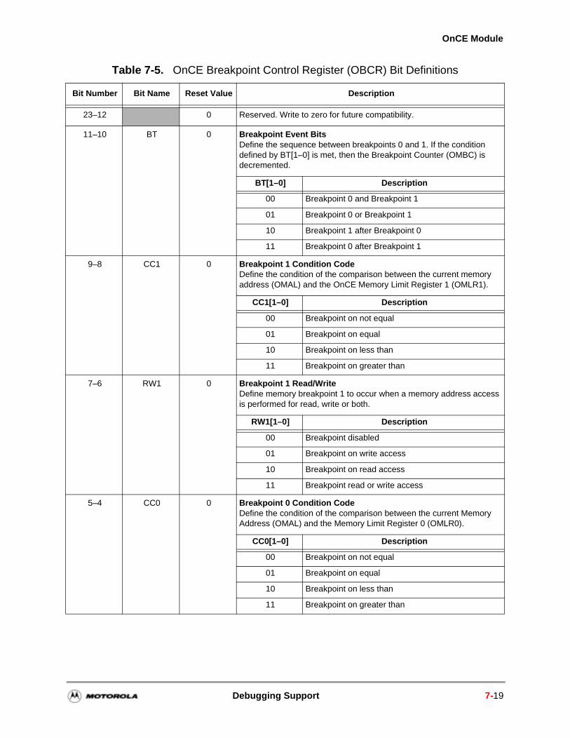
OnCE Module
Table 7-5. OnCE Breakpoint Control Register (OBCR) Bit Definitions
Bit Number Bit Name Reset Value Description
23–12 0 Reserved. Write to zero for future compatibility.
11–10 BT 0 Breakpoint Event Bits Define the sequence between breakpoints 0 and 1. If the condition defined by BT[1–0] is met, then the Breakpoint Counter (OMBC) is decremented.
BT[1–0] Description
00 Breakpoint 0 and Breakpoint 1
01 Breakpoint 0 or Breakpoint 1
10 Breakpoint 1 after Breakpoint 0
11 Breakpoint 0 after Breakpoint 1
9–8 CC1 0 Breakpoint 1 Condition CodeDefine the condition of the comparison between the current memory address (OMAL) and the OnCE Memory Limit Register 1 (OMLR1).
CC1[1–0] Description
00 Breakpoint on not equal
01 Breakpoint on equal
10 Breakpoint on less than
11 Breakpoint on greater than
7–6 RW1 0 Breakpoint 1 Read/WriteDefine memory breakpoint 1 to occur when a memory address access is performed for read, write or both.
RW1[1–0] Description
00 Breakpoint disabled
01 Breakpoint on write access
10 Breakpoint on read access
11 Breakpoint read or write access
5–4 CC0 0 Breakpoint 0 Condition CodeDefine the condition of the comparison between the current Memory Address (OMAL) and the Memory Limit Register 0 (OMLR0).
CC0[1–0] Description
00 Breakpoint on not equal
01 Breakpoint on equal
10 Breakpoint on less than
11 Breakpoint on greater than
Debugging Support 7-19
Debugging Support
7.2.2.1 OnCE Memory Breakpoint Counter (OMBC)
The OnCE Memory Breakpoint Counter is a 24-bit counter that is loaded with a value equal to the number of times minus one that a memory access event should occur before a memory breakpoint is declared. The memory access event is specified by the OBCR and by the memory limit registers. On each occurrence of the memory access event, the breakpoint counter decrements. When the counter reaches 0 and a new event occurs, the chip enters Debug mode. The OMBC can be read or written through the JTAG port. Each time the limit register changes or a different breakpoint event is selected in the OBCR, the breakpoint counter must be written afterwards. This ensures that the OnCE breakpoint logic is reset and that no previous events can affect the new breakpoint event selected. The breakpoint counter is cleared by hardware reset.
7.2.3 Cache Support
To keep track of the cache contents and status, the eight Tag values, Tag lock/unlock status, and LRU status can be read via the OnCE module. Nine 24-bit registers are implemented as a circular buffer with a 4-bit counter. All registers have the same address, but any access to the Tag buffer increments the counter, thus pointing to the next register in the circular buffer. When Debug mode is exited, the counter is cleared, so when Debug mode is re-entered, the first read from the Tag buffer address always starts from the first
3–2 RW0 0 Breakpoint 0 Read/WriteDefine the memory breakpoint 0 to occur when a memory address access is performed for read, write, or both.
RW0[1–0] Description
00 Breakpoint disabled
01 Breakpoint on write access
10 Breakpoint on read access
11 Breakpoint on read or write access
1–0 MBS 0 Memory BreakpointEnable memory breakpoints 0 and 1, allowing them to occur when a memory access is performed on P, X, or Y memory.
MBS[1–0] Description
00 Reserved
01 Breakpoint on P access
10 Breakpoint on X access
11 Breakpoint on Y access
Table 7-5. OnCE Breakpoint Control Register (OBCR) Bit Definitions (Continued)
Bit Number Bit Name Reset Value Description
7-20 DSP56300 Family Manual
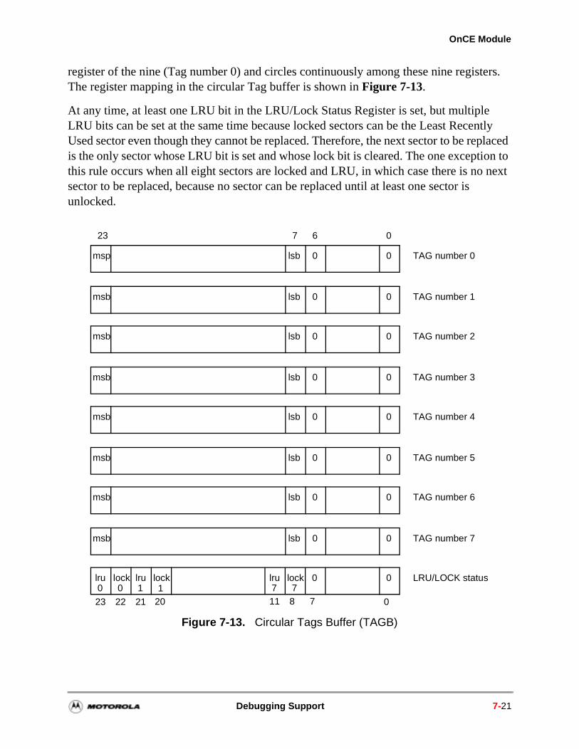
OnCE Module
register of the nine (Tag number 0) and circles continuously among these nine registers. The register mapping in the circular Tag buffer is shown in Figure 7-13.
At any time, at least one LRU bit in the LRU/Lock Status Register is set, but multiple LRU bits can be set at the same time because locked sectors can be the Least Recently Used sector even though they cannot be replaced. Therefore, the next sector to be replaced is the only sector whose LRU bit is set and whose lock bit is cleared. The one exception to this rule occurs when all eight sectors are locked and LRU, in which case there is no next sector to be replaced, because no sector can be replaced until at least one sector is unlocked.
Figure 7-13. Circular Tags Buffer (TAGB)
TAG number 0
023
msp lsb 0 0
7 6
TAG number 1msb lsb 0 0
TAG number 2msb lsb 0 0
TAG number 3msb lsb 0 0
TAG number 4msb lsb 0 0
TAG number 5msb lsb 0 0
TAG number 6msb lsb 0 0
TAG number 7msb lsb 0 0
lock lock 0 00 0 1 7 7lru lru lru LRU/LOCK status
23 22 21 811 7 0
lock1
20
Debugging Support 7-21
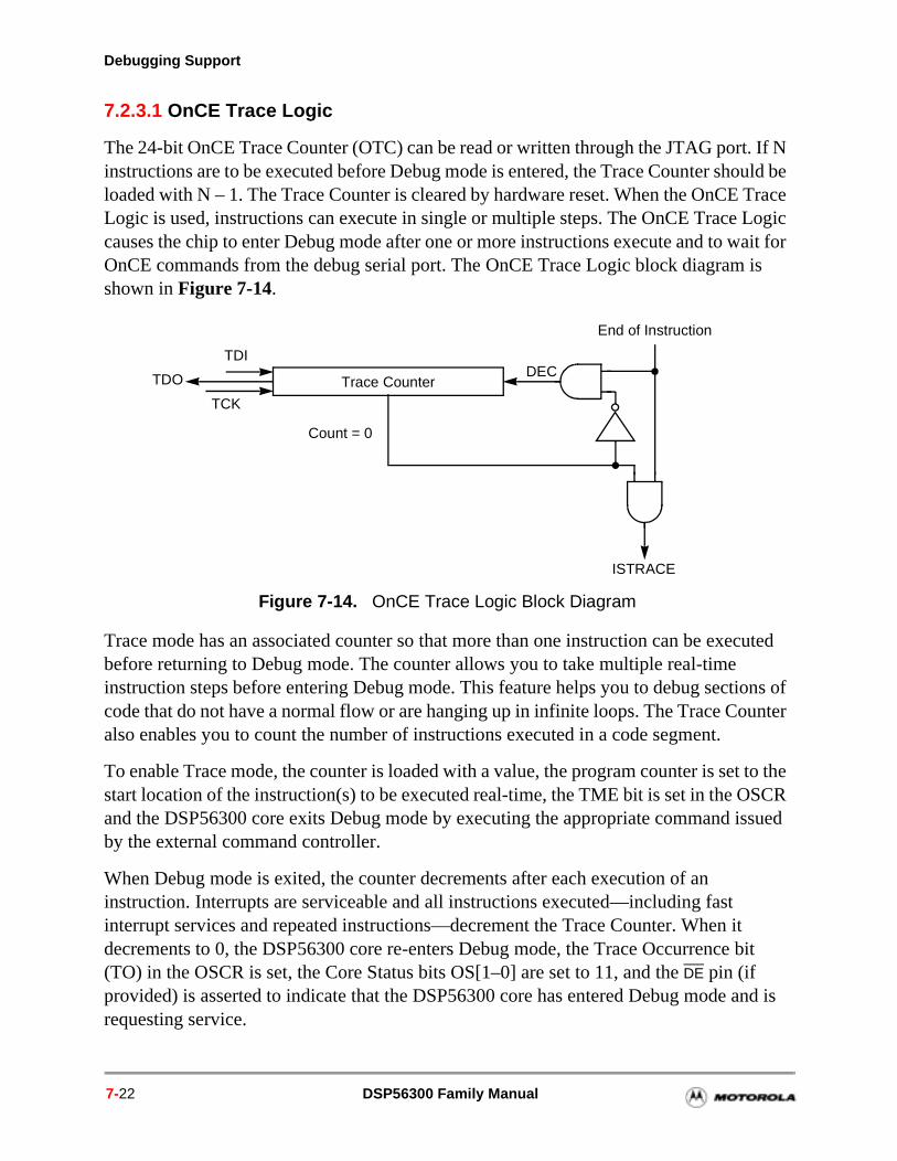
Debugging Support
Trace Logic ait for
is
cuted
ions of unter
t to the SCR issued
t bit
and is
7.2.3.1 OnCE Trace Logic
The 24-bit OnCE Trace Counter (OTC) can be read or written through the JTAG port. If N instructions are to be executed before Debug mode is entered, the Trace Counter should be loaded with N – 1. The Trace Counter is cleared by hardware reset. When the OnCELogic is used, instructions can execute in single or multiple steps. The OnCE Trace causes the chip to enter Debug mode after one or more instructions execute and to wOnCE commands from the debug serial port. The OnCE Trace Logic block diagramshown in Figure 7-14.
Figure 7-14. OnCE Trace Logic Block Diagram
Trace mode has an associated counter so that more than one instruction can be exebefore returning to Debug mode. The counter allows you to take multiple real-time instruction steps before entering Debug mode. This feature helps you to debug sectcode that do not have a normal flow or are hanging up in infinite loops. The Trace Coalso enables you to count the number of instructions executed in a code segment.
To enable Trace mode, the counter is loaded with a value, the program counter is sestart location of the instruction(s) to be executed real-time, the TME bit is set in the Oand the DSP56300 core exits Debug mode by executing the appropriate command by the external command controller.
When Debug mode is exited, the counter decrements after each execution of an instruction. Interrupts are serviceable and all instructions executed—including fast interrupt services and repeated instructions—decrement the Trace Counter. When idecrements to 0, the DSP56300 core re-enters Debug mode, the Trace Occurrence(TO) in the OSCR is set, the Core Status bits OS[1–0] are set to 11, and the DE pin (if provided) is asserted to indicate that the DSP56300 core has entered Debug mode requesting service.
TDI
TDO
TCK
Trace CounterDEC
End of Instruction
Count = 0
ISTRACE
7-22 DSP56300 Family Manual
OnCE Module
7.2.4 Methods of Entering Debug Mode
The chip acknowledges entering Debug mode by setting the Core Status bits OS1 and OS0 and asserting the DE line. This informs the external command controller that the chip is in Debug mode and awaiting commands. The DSP56300 core can disable the OnCE module if the ROM Security option is implemented. If the ROM Security is implemented, the OnCE module remains inactive until the DSP56300 core executes a write operation to the OGDBR. Following is a list of ways to enter Debug mode:
External Debug Request During RESET Assertion: Holding the DE line asserted during the assertion of RESET causes the chip to enter the Debug mode. After receiving the acknowledge, the external command controller must negate the DE line before sending the first command. In this case, the chip does not execute any instruction before entering the Debug mode.
External Debug Request During Normal Activity: Holding the DE line asserted during normal chip activity causes the chip to finish executing the current instruction and then enter Debug mode. After receiving the acknowledge, the external command controller must negate the DE line before sending the first command. This process is the same for any newly fetched instruction, including instructions fetched by the interrupt processing or instructions that are aborted by the interrupt processing. In this case the chip finishes executing the current instruction and stops after the newly fetched instruction enters the instruction latch.
Executing the JTAG DEBUG_REQUEST Instruction: Executing the JTAG instruction DEBUG_REQUEST asserts an internal debug request signal. The chip finishes executing the current instruction and stops after the newly fetched instruction enters the instruction latch. After entering the Debug mode, the Core Status bits OS1 and OS0 are set and the DE line is asserted, thus acknowledging the external command controller that the Debug mode of operation has been entered.
External Debug Request During Stop: Executing the JTAG instruction DEBUG_REQUEST (or asserting DE) while the chip is in Stop state (that is, has executed a STOP instruction) causes the chip to exit the Stop state and enter Debug mode. After receiving the acknowledge, the external command controller must negate DE before sending the first command. In this case, the chip finishes executing the STOP instruction and halts after the next instruction enters the instruction latch.
External Debug Request During Wait: Executing the JTAG instruction DEBUG_REQUEST (or asserting DE) while the chip is in the Wait state (that is, has executed a WAIT instruction) causes the chip to exit the Wait state and enter Debug mode. After receiving the acknowledge, the external command controller must negate DE before sending the first command. In this case, the chip completes
Debugging Support 7-23
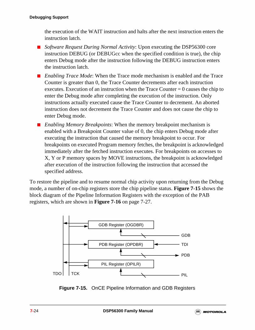
Debugging Support
the execution of the WAIT instruction and halts after the next instruction enters the instruction latch.
Software Request During Normal Activity: Upon executing the DSP56300 core instruction DEBUG (or DEBUGcc when the specified condition is true), the chip enters Debug mode after the instruction following the DEBUG instruction enters the instruction latch.
Enabling Trace Mode: When the Trace mode mechanism is enabled and the Trace Counter is greater than 0, the Trace Counter decrements after each instruction executes. Execution of an instruction when the Trace Counter = 0 causes the chip to enter the Debug mode after completing the execution of the instruction. Only instructions actually executed cause the Trace Counter to decrement. An aborted instruction does not decrement the Trace Counter and does not cause the chip to enter Debug mode.
Enabling Memory Breakpoints: When the memory breakpoint mechanism is enabled with a Breakpoint Counter value of 0, the chip enters Debug mode after executing the instruction that caused the memory breakpoint to occur. For breakpoints on executed Program memory fetches, the breakpoint is acknowledged immediately after the fetched instruction executes. For breakpoints on accesses to X, Y or P memory spaces by MOVE instructions, the breakpoint is acknowledged after execution of the instruction following the instruction that accessed the specified address.
To restore the pipeline and to resume normal chip activity upon returning from the Debug mode, a number of on-chip registers store the chip pipeline status. Figure 7-15 shows the block diagram of the Pipeline Information Registers with the exception of the PAB registers, which are shown in Figure 7-16 on page 7-27.
Figure 7-15. OnCE Pipeline Information and GDB Registers
PDB Register (OPDBR)
GDB Register (OGDBR)
TDI
TDO TCK
PIL Register (OPILR)
PIL
PDB
GDB
7-24 DSP56300 Family Manual
OnCE Module
OnCE PDB Register (OPDBR): A 24-bit latch that stores the value of the Program Data Bus generated by the last program memory access of the core before Debug mode is entered. The OPDBR is read or written through the JTAG port. This register is affected by the operations performed during the Debug mode and must be restored by the external command controller when returning to Normal mode.
OnCE PIL Register (OPILR): A 24-bit latch that stores the value of the Instruction Latch before Debug mode is entered. OPILR can only be read through the JTAG port. Since the Instruction Latch is affected by the operations performed during Debug mode, it must be restored by the external command controller when returning to Normal mode. Since there is no direct write access to the Instruction Latch, restoration is accomplished by writing to the OPDBR with no-GO and no-EX. The data written on PDB is transferred into the Instruction Latch.
OnCE GDB Register (OGDBR): A 24-bit latch that can only be read through the JTAG port. The OGDBR is not actually required for a pipeline status restore, but is required for passing information between the chip and the external command controller. The OGDBR is mapped on the X internal I/O space at address $FFFFFC. When the external command controller needs the contents of a register or memory location, it forces the chip to execute an instruction that brings this information to the OGDBR. Then the contents of the OGDBR are delivered serially to the external command controller by the command READ GDB REGISTER.
7.2.5 Trace Buffer
To ease debugging activity and keep track of program flow, the DSP56300 core provides a number of on-chip dedicated resources. Three read-only PAB registers give pipeline information when Debug mode is entered, and a Trace Buffer stores the address of the last instruction executed, as well as the addresses of the last eight change of flow instructions.
OnCE PAB Register for Fetch (OPABFR): A 24-bit register that stores the address of the last instruction whose fetch started before Debug mode was entered. The OPABFR can only be read through the JTAG port. This register is not affected by the operations performed during Debug mode.
PAB Register for Decode (OPABDR): A 24-bit register that stores the address of the instruction currently on the PDB. This is the instruction whose fetch completed before the chip entered Debug mode. The OPABDR can only be read through the JTAG port. This register is not affected by the operations performed during Debug mode.
PAB Register for Execute (OPABEX): A 24-bit register that stores the address of the instruction currently in the Instruction Latch. This is the instruction that would have decoded and executed if the chip had not entered Debug mode. The OPABEX
Debugging Support 7-25
Debugging Support
register can only be read through the JTAG port. This register is not affected by the operations performed during Debug mode.
The Trace Buffer stores the addresses of the last twelve change of flow instructions that executed, as well as the address of the last executed instruction. It is implemented as a circular buffer containing twelve 25-bit registers and one 4-bit counter. All the registers have the same address, but any read access to the Trace Buffer address causes the counter to increment, thus pointing to the next Trace Buffer register. The registers are serially available to the external command controller through their common Trace Buffer address. Figure 7-16 shows the block diagram of the Trace Buffer. The Trace Buffer is not affected by the operations performed during Debug mode except for the Trace Buffer pointer increment when reading the Trace Buffer. When Debug mode is entered, the Trace Buffer counter points to the Trace Buffer register containing the address of the last executed instructions. The first Trace Buffer read obtains the oldest address and the following Trace Buffer reads get the other addresses from the oldest to the newest, in order of execution.
Note: To ensure Trace Buffer coherence, a complete set of twelve reads of the Trace Buffer must be performed because each read increments the Trace Buffer pointer, thus pointing to the next location. After twelve reads, the pointer indicates the same location as before starting the read procedure.
Note: On any change of flow instruction, the Trace Buffer stores both the address of the change of flow instruction, as well as the address of the target of the change of flow instruction. In the case of conditional change of flows, the address of the change of flow instruction is always stored (regardless of the fact that the change of flow is true or false), but if the conditional change of flow is false (that is, not taken) the address of the target is not stored. In order to facilitate the program trace reconstruction, every Trace Buffer location has an additional invalid bit (the 25th bit). If a conditional change of flow instruction has a condition false, the invalid bit is set, thus marking this instruction as not taken. Therefore, it is imperative to read twenty-five bits of data when reading the twelve Trace Buffer registers. Since data is read LSB first, the invalid bit is the first bit to be read.
7.2.6 OnCE Commands and Serial Protocol
To permit an efficient means of communication between the external command controller and the DSP56300 core chip, the following protocol is adopted. Before starting any debugging activity, the external command controller must wait for an acknowledge on the DE line indicating that the chip has entered Debug mode (optionally the external command controller can poll the OS1 and OS0 bits in the JTAG instruction shift register). The
7-26 DSP56300 Family Manual
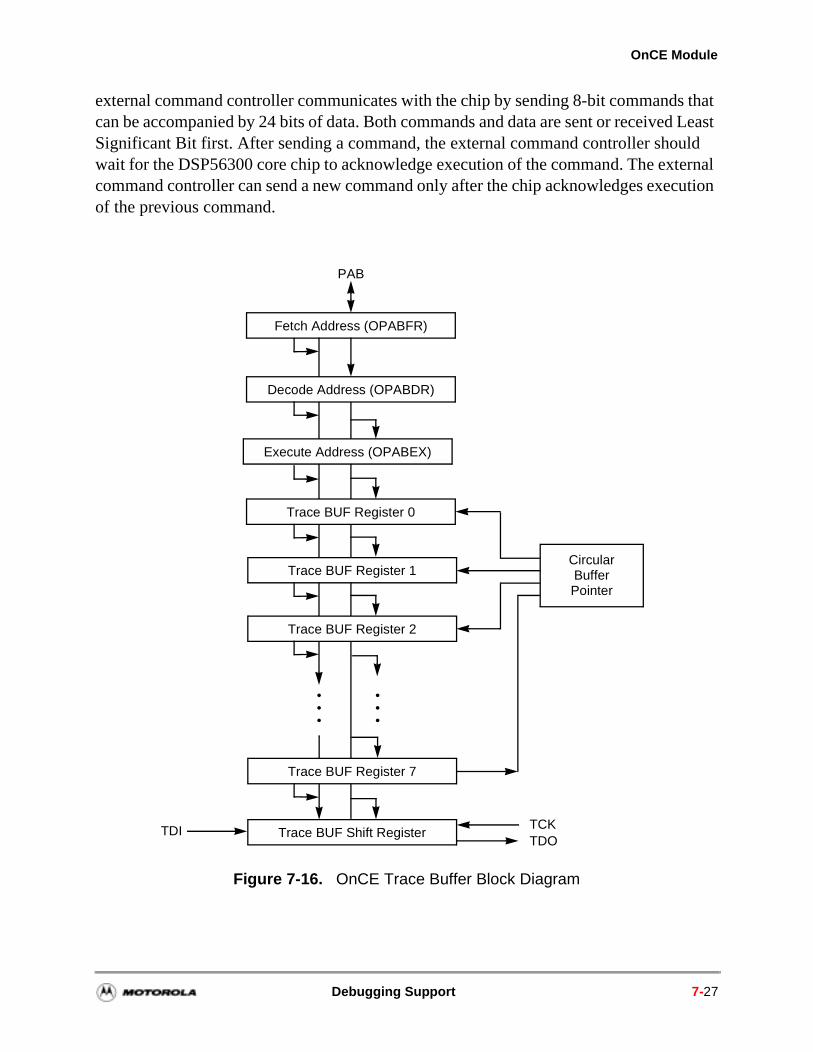
OnCE Module
external command controller communicates with the chip by sending 8-bit commands that can be accompanied by 24 bits of data. Both commands and data are sent or received Least Significant Bit first. After sending a command, the external command controller should wait for the DSP56300 core chip to acknowledge execution of the command. The external command controller can send a new command only after the chip acknowledges execution of the previous command.
Figure 7-16. OnCE Trace Buffer Block Diagram
Fetch Address (OPABFR)
PAB
Decode Address (OPABDR)
CircularBufferPointer
Trace BUF Shift RegisterTDOTCK
Trace BUF Register 0
Trace BUF Register 1
Trace BUF Register 2
Trace BUF Register 7
Execute Address (OPABEX)
TDI
Debugging Support 7-27
Debugging Support
value
he ensing
The OnCE commands are classified as follows:
Read commands (when the chip delivers the required data)
Write commands (when the chip receives data and writes the data in one of the OnCE registers)
Commands that do not have data transfers associated with them
The commands are 8 bits long and have the format shown in Figure 7-9, OnCE Command Register (OCR), on page 7-13.
7.2.7 OnCE Module Examples
The following examples of debugging procedures using the OnCE module assume that the DSP is the only device in the JTAG chain. If more than one device in the chain exists (other DSPs or even other devices), the other devices can be forced to execute the JTAG BYPASS instruction so that their effect in the serial stream is one bit per additional device. The events select-DR, select-IR, update-DR, shift-DR, and so on refer to bringing the JTAG TAP in the corresponding state.
7.2.7.1 Checking Whether the Chip Has Entered Debug Mode
There are two methods of verifying that the chip has entered Debug mode:
Every time the chip enters Debug mode, a pulse is generated on the DE line. A pulse is also generated every time the chip acknowledges the execution of an instruction in Debug mode. An external command controller can connect the DE line to an interrupt pin to sense the acknowledge.
An external command controller can poll the JTAG instruction shift register for the status bits OS[1–0]. When the chip is in Debug mode these bits are set to the11.
In the following paragraphs, the ACK notation denotes the operation performed by tcommand controller to check whether the chip has entered Debug mode (either by sDE or by polling JTAG instruction shift register).
7-28 DSP56300 Family Manual
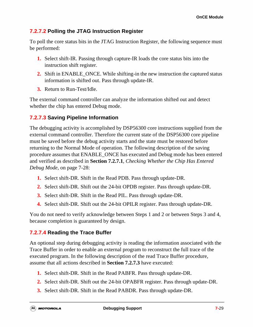
OnCE Module
7.2.7.2 Polling the JTAG Instruction Register
To poll the core status bits in the JTAG Instruction Register, the following sequence must be performed:
1. Select shift-IR. Passing through capture-IR loads the core status bits into the instruction shift register.
2. Shift in ENABLE_ONCE. While shifting-in the new instruction the captured status information is shifted out. Pass through update-IR.
3. Return to Run-Test/Idle.
The external command controller can analyze the information shifted out and detect whether the chip has entered Debug mode.
7.2.7.3 Saving Pipeline Information
The debugging activity is accomplished by DSP56300 core instructions supplied from the external command controller. Therefore the current state of the DSP56300 core pipeline must be saved before the debug activity starts and the state must be restored before returning to the Normal Mode of operation. The following description of the saving procedure assumes that ENABLE_ONCE has executed and Debug mode has been entered and verified as described in Section 7.2.7.1, Checking Whether the Chip Has Entered Debug Mode, on page 7-28:
1. Select shift-DR. Shift in the Read PDB. Pass through update-DR.
2. Select shift-DR. Shift out the 24-bit OPDB register. Pass through update-DR.
3. Select shift-DR. Shift in the Read PIL. Pass through update-DR.
4. Select shift-DR. Shift out the 24-bit OPILR register. Pass through update-DR.
You do not need to verify acknowledge between Steps 1 and 2 or between Steps 3 and 4, because completion is guaranteed by design.
7.2.7.4 Reading the Trace Buffer
An optional step during debugging activity is reading the information associated with the Trace Buffer in order to enable an external program to reconstruct the full trace of the executed program. In the following description of the read Trace Buffer procedure, assume that all actions described in Section 7.2.7.3 have executed:
1. Select shift-DR. Shift in the Read PABFR. Pass through update-DR.
2. Select shift-DR. Shift out the 24-bit OPABFR register. Pass through update-DR.
3. Select shift-DR. Shift in the Read PABDR. Pass through update-DR.
Debugging Support 7-29
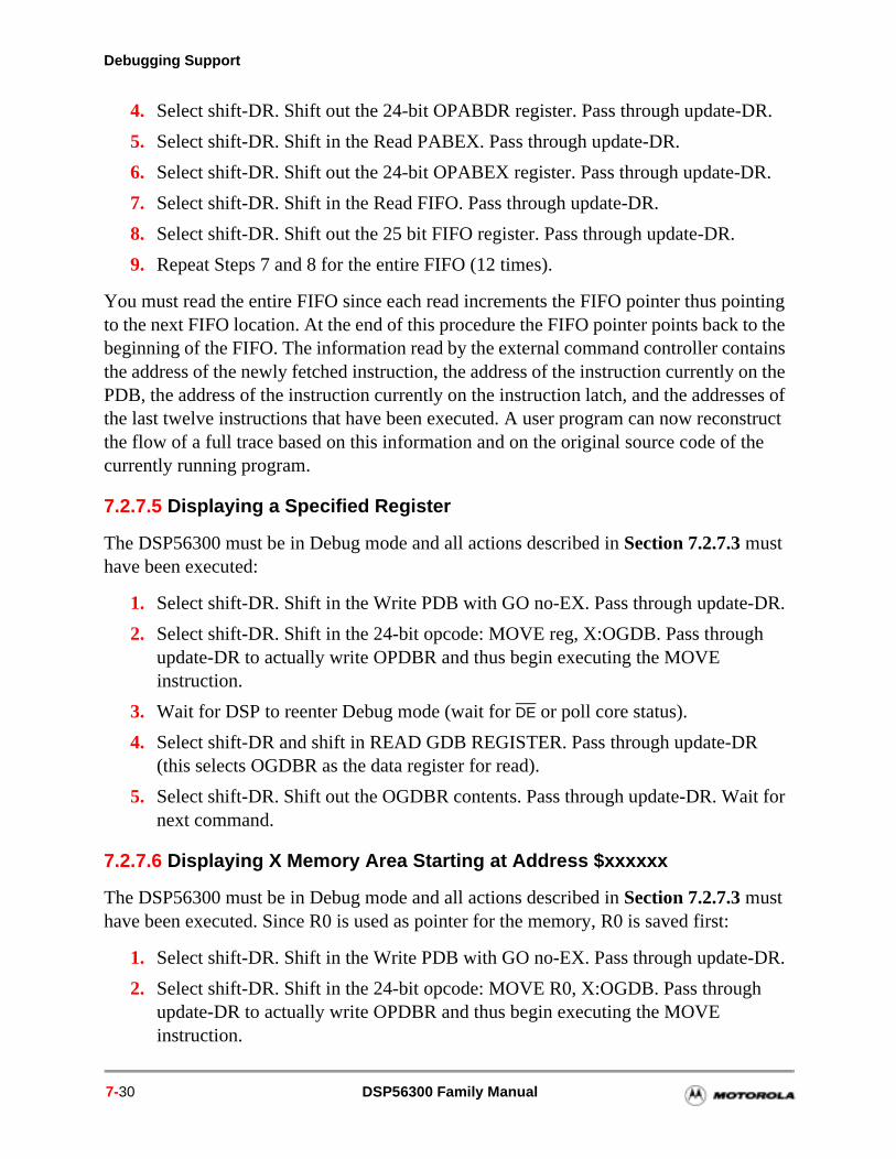
Debugging Support
4. Select shift-DR. Shift out the 24-bit OPABDR register. Pass through update-DR.
5. Select shift-DR. Shift in the Read PABEX. Pass through update-DR.
6. Select shift-DR. Shift out the 24-bit OPABEX register. Pass through update-DR.
7. Select shift-DR. Shift in the Read FIFO. Pass through update-DR.
8. Select shift-DR. Shift out the 25 bit FIFO register. Pass through update-DR.
9. Repeat Steps 7 and 8 for the entire FIFO (12 times).
You must read the entire FIFO since each read increments the FIFO pointer thus pointing to the next FIFO location. At the end of this procedure the FIFO pointer points back to the beginning of the FIFO. The information read by the external command controller contains the address of the newly fetched instruction, the address of the instruction currently on the PDB, the address of the instruction currently on the instruction latch, and the addresses of the last twelve instructions that have been executed. A user program can now reconstruct the flow of a full trace based on this information and on the original source code of the currently running program.
7.2.7.5 Displaying a Specified Register
The DSP56300 must be in Debug mode and all actions described in Section 7.2.7.3 must have been executed:
1. Select shift-DR. Shift in the Write PDB with GO no-EX. Pass through update-DR.
2. Select shift-DR. Shift in the 24-bit opcode: MOVE reg, X:OGDB. Pass through update-DR to actually write OPDBR and thus begin executing the MOVE instruction.
3. Wait for DSP to reenter Debug mode (wait for DE or poll core status).
4. Select shift-DR and shift in READ GDB REGISTER. Pass through update-DR (this selects OGDBR as the data register for read).
5. Select shift-DR. Shift out the OGDBR contents. Pass through update-DR. Wait for next command.
7.2.7.6 Displaying X Memory Area Starting at Address $xxxxxx
The DSP56300 must be in Debug mode and all actions described in Section 7.2.7.3 must have been executed. Since R0 is used as pointer for the memory, R0 is saved first:
1. Select shift-DR. Shift in the Write PDB with GO no-EX. Pass through update-DR.
2. Select shift-DR. Shift in the 24-bit opcode: MOVE R0, X:OGDB. Pass through update-DR to actually write OPDBR and thus begin executing the MOVE instruction.
7-30 DSP56300 Family Manual
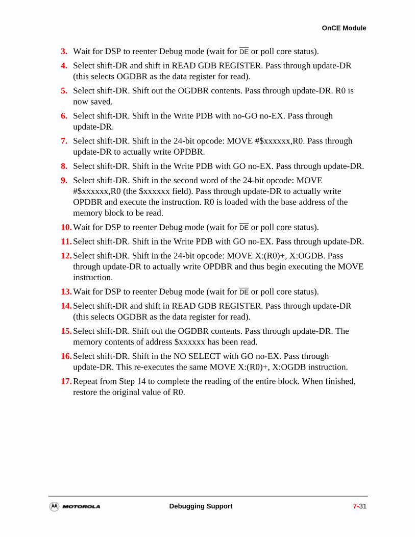
OnCE Module
3. Wait for DSP to reenter Debug mode (wait for DE or poll core status).
4. Select shift-DR and shift in READ GDB REGISTER. Pass through update-DR (this selects OGDBR as the data register for read).
5. Select shift-DR. Shift out the OGDBR contents. Pass through update-DR. R0 is now saved.
6. Select shift-DR. Shift in the Write PDB with no-GO no-EX. Pass through update-DR.
7. Select shift-DR. Shift in the 24-bit opcode: MOVE #$xxxxxx,R0. Pass through update-DR to actually write OPDBR.
8. Select shift-DR. Shift in the Write PDB with GO no-EX. Pass through update-DR.
9. Select shift-DR. Shift in the second word of the 24-bit opcode: MOVE #$xxxxxx,R0 (the $xxxxxx field). Pass through update-DR to actually write OPDBR and execute the instruction. R0 is loaded with the base address of the memory block to be read.
10. Wait for DSP to reenter Debug mode (wait for DE or poll core status).
11. Select shift-DR. Shift in the Write PDB with GO no-EX. Pass through update-DR.
12. Select shift-DR. Shift in the 24-bit opcode: MOVE X:(R0)+, X:OGDB. Pass through update-DR to actually write OPDBR and thus begin executing the MOVE instruction.
13. Wait for DSP to reenter Debug mode (wait for DE or poll core status).
14. Select shift-DR and shift in READ GDB REGISTER. Pass through update-DR (this selects OGDBR as the data register for read).
15. Select shift-DR. Shift out the OGDBR contents. Pass through update-DR. The memory contents of address $xxxxxx has been read.
16. Select shift-DR. Shift in the NO SELECT with GO no-EX. Pass through update-DR. This re-executes the same MOVE X:(R0)+, X:OGDB instruction.
17. Repeat from Step 14 to complete the reading of the entire block. When finished, restore the original value of R0.
Debugging Support 7-31
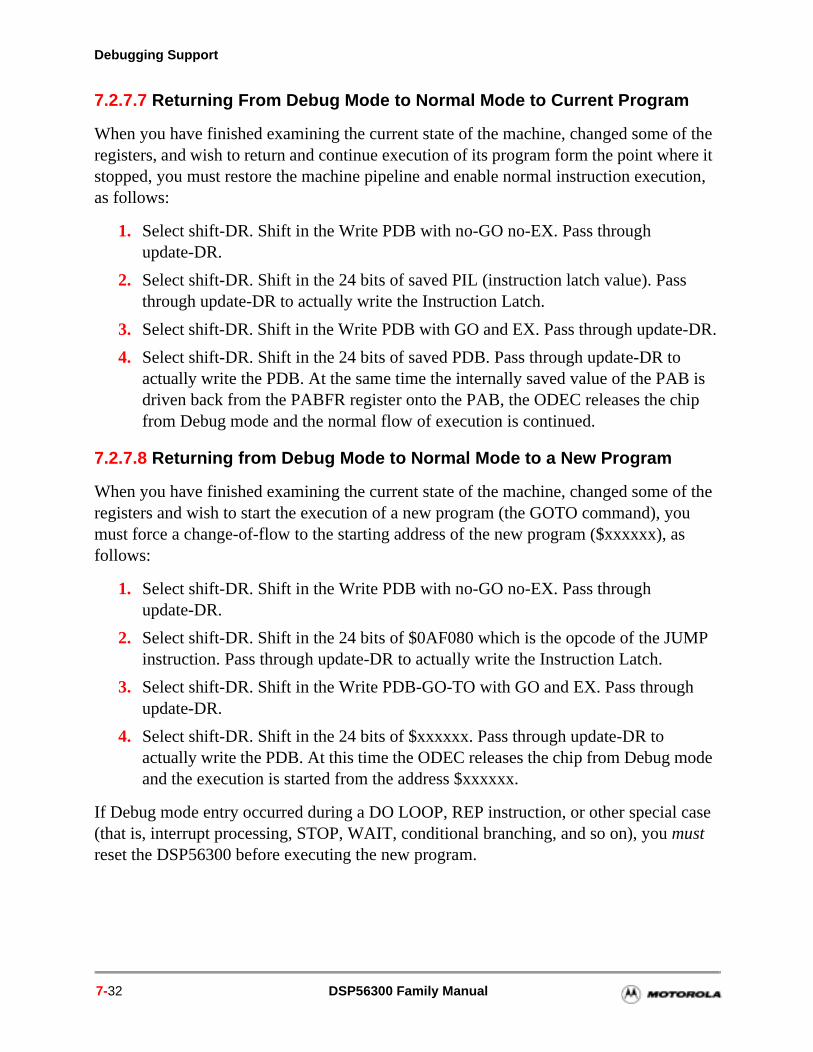
Debugging Support
7.2.7.7 Returning From Debug Mode to Normal Mode to Current Program
When you have finished examining the current state of the machine, changed some of the registers, and wish to return and continue execution of its program form the point where it stopped, you must restore the machine pipeline and enable normal instruction execution, as follows:
1. Select shift-DR. Shift in the Write PDB with no-GO no-EX. Pass through update-DR.
2. Select shift-DR. Shift in the 24 bits of saved PIL (instruction latch value). Pass through update-DR to actually write the Instruction Latch.
3. Select shift-DR. Shift in the Write PDB with GO and EX. Pass through update-DR.
4. Select shift-DR. Shift in the 24 bits of saved PDB. Pass through update-DR to actually write the PDB. At the same time the internally saved value of the PAB is driven back from the PABFR register onto the PAB, the ODEC releases the chip from Debug mode and the normal flow of execution is continued.
7.2.7.8 Returning from Debug Mode to Normal Mode to a New Program
When you have finished examining the current state of the machine, changed some of the registers and wish to start the execution of a new program (the GOTO command), you must force a change-of-flow to the starting address of the new program ($xxxxxx), as follows:
1. Select shift-DR. Shift in the Write PDB with no-GO no-EX. Pass through update-DR.
2. Select shift-DR. Shift in the 24 bits of $0AF080 which is the opcode of the JUMP instruction. Pass through update-DR to actually write the Instruction Latch.
3. Select shift-DR. Shift in the Write PDB-GO-TO with GO and EX. Pass through update-DR.
4. Select shift-DR. Shift in the 24 bits of $xxxxxx. Pass through update-DR to actually write the PDB. At this time the ODEC releases the chip from Debug mode and the execution is started from the address $xxxxxx.
If Debug mode entry occurred during a DO LOOP, REP instruction, or other special case (that is, interrupt processing, STOP, WAIT, conditional branching, and so on), you must reset the DSP56300 before executing the new program.
7-32 DSP56300 Family Manual
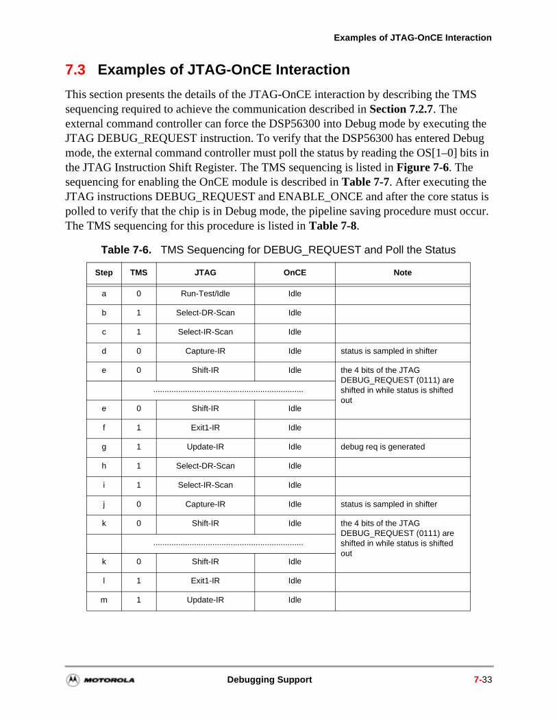
Examples of JTAG-OnCE Interaction
bits in
s is ccur.
7.3 Examples of JTAG-OnCE Interaction
This section presents the details of the JTAG-OnCE interaction by describing the TMS sequencing required to achieve the communication described in Section 7.2.7. The external command controller can force the DSP56300 into Debug mode by executing the JTAG DEBUG_REQUEST instruction. To verify that the DSP56300 has entered Debug mode, the external command controller must poll the status by reading the OS[1–0] the JTAG Instruction Shift Register. The TMS sequencing is listed in Figure 7-6. The sequencing for enabling the OnCE module is described in Table 7-7. After executing the JTAG instructions DEBUG_REQUEST and ENABLE_ONCE and after the core statupolled to verify that the chip is in Debug mode, the pipeline saving procedure must oThe TMS sequencing for this procedure is listed in Table 7-8.
Table 7-6. TMS Sequencing for DEBUG_REQUEST and Poll the Status
Step TMS JTAG OnCE Note
a 0 Run-Test/Idle Idle
b 1 Select-DR-Scan Idle
c 1 Select-IR-Scan Idle
d 0 Capture-IR Idle status is sampled in shifter
e 0 Shift-IR Idle the 4 bits of the JTAG DEBUG_REQUEST (0111) are shifted in while status is shifted out
..................................................................
e 0 Shift-IR Idle
f 1 Exit1-IR Idle
g 1 Update-IR Idle debug req is generated
h 1 Select-DR-Scan Idle
i 1 Select-IR-Scan Idle
j 0 Capture-IR Idle status is sampled in shifter
k 0 Shift-IR Idle the 4 bits of the JTAG DEBUG_REQUEST (0111) are shifted in while status is shifted out
..................................................................
k 0 Shift-IR Idle
l 1 Exit1-IR Idle
m 1 Update-IR Idle
Debugging Support 7-33
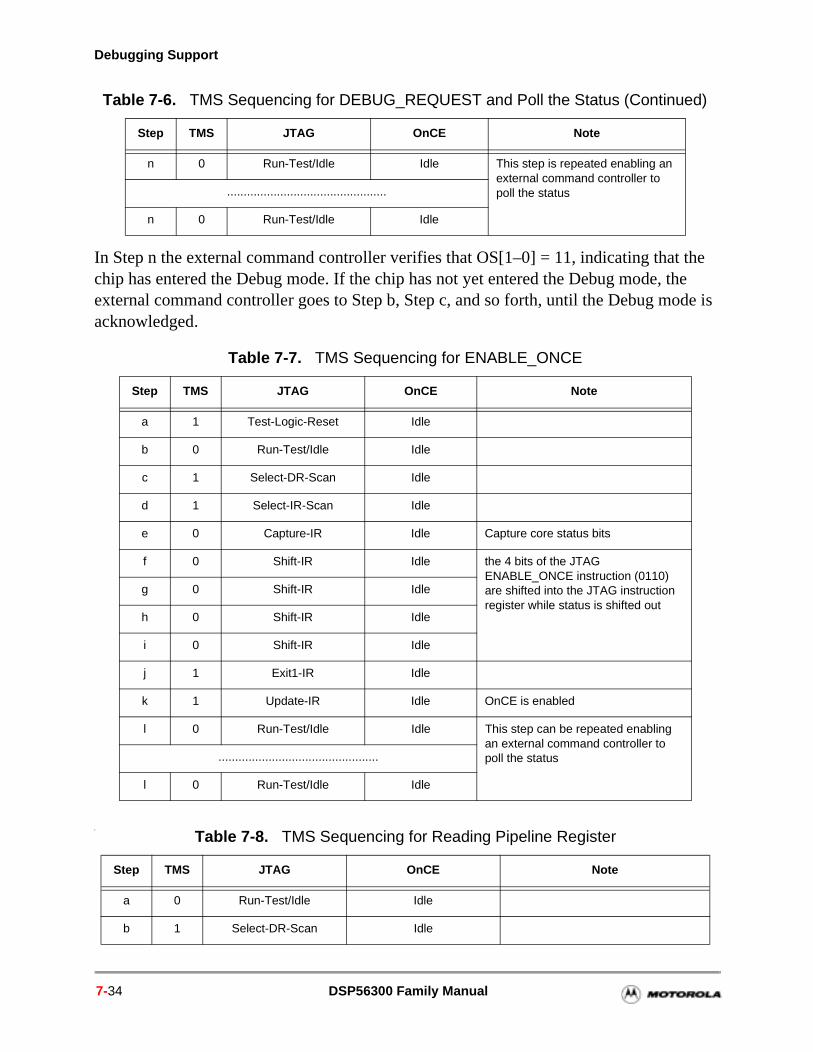
Debugging Support
the the ode is
In Step n the external command controller verifies that OS[1–0] = 11, indicating thatchip has entered the Debug mode. If the chip has not yet entered the Debug mode, external command controller goes to Step b, Step c, and so forth, until the Debug macknowledged.
s
n 0 Run-Test/Idle Idle This step is repeated enabling an external command controller to poll the status................................................
n 0 Run-Test/Idle Idle
Table 7-7. TMS Sequencing for ENABLE_ONCE
Step TMS JTAG OnCE Note
a 1 Test-Logic-Reset Idle
b 0 Run-Test/Idle Idle
c 1 Select-DR-Scan Idle
d 1 Select-IR-Scan Idle
e 0 Capture-IR Idle Capture core status bits
f 0 Shift-IR Idle the 4 bits of the JTAG ENABLE_ONCE instruction (0110) are shifted into the JTAG instruction register while status is shifted out
g 0 Shift-IR Idle
h 0 Shift-IR Idle
i 0 Shift-IR Idle
j 1 Exit1-IR Idle
k 1 Update-IR Idle OnCE is enabled
l 0 Run-Test/Idle Idle This step can be repeated enabling an external command controller to poll the status................................................
l 0 Run-Test/Idle Idle
Table 7-8. TMS Sequencing for Reading Pipeline Register
Step TMS JTAG OnCE Note
a 0 Run-Test/Idle Idle
b 1 Select-DR-Scan Idle
Table 7-6. TMS Sequencing for DEBUG_REQUEST and Poll the Status (Continued)
Step TMS JTAG OnCE Note
7-34 DSP56300 Family Manual

Examples of JTAG-OnCE Interaction
c 0 Capture-DR Idle
d 0 Shift-DR Idle the 8 bits of the OnCE “Read PIL” (10001011) are shifted in
..................................................................
d 0 Shift-DR Idle
e 1 Exit1-DR Idle
f 1 Update-DR Execute “Read PIL” PIL value is loaded in shifter
g 1 Select-DR-Scan Idle
h 0 Capture-DR Idle
i 0 Shift-DR Idle the 24 bits of the PIL are shifted out (24 steps)
..................................................................
i 0 Shift-DR Idle
j 1 Exit1-DR Idle
k 1 Update-DR Idle
l 1 Select-DR-Scan Idle
m 0 Capture-DR Idle
n 0 Shift-DR Idle the 8 bits of the OnCE “Read PDB” (10001010) are shifted in
..................................................................
n 0 Shift-DR Idle
o 1 Exit1-DR Idle
p 1 Update-DR Execute “Read PDB” PDB value is loaded in shifter
q 1 Select-DR-Scan Idle
r 0 Capture-DR Idle
s 0 Shift-DR Idle The 24 bits of the PDB are shifted out (24 steps)
..................................................................
s 0 Shift-DR Idle
t 1 Exit1-DR Idle
u 1 Update-DR Idle
Table 7-8. TMS Sequencing for Reading Pipeline Register (Continued)
Step TMS JTAG OnCE Note
Debugging Support 7-35
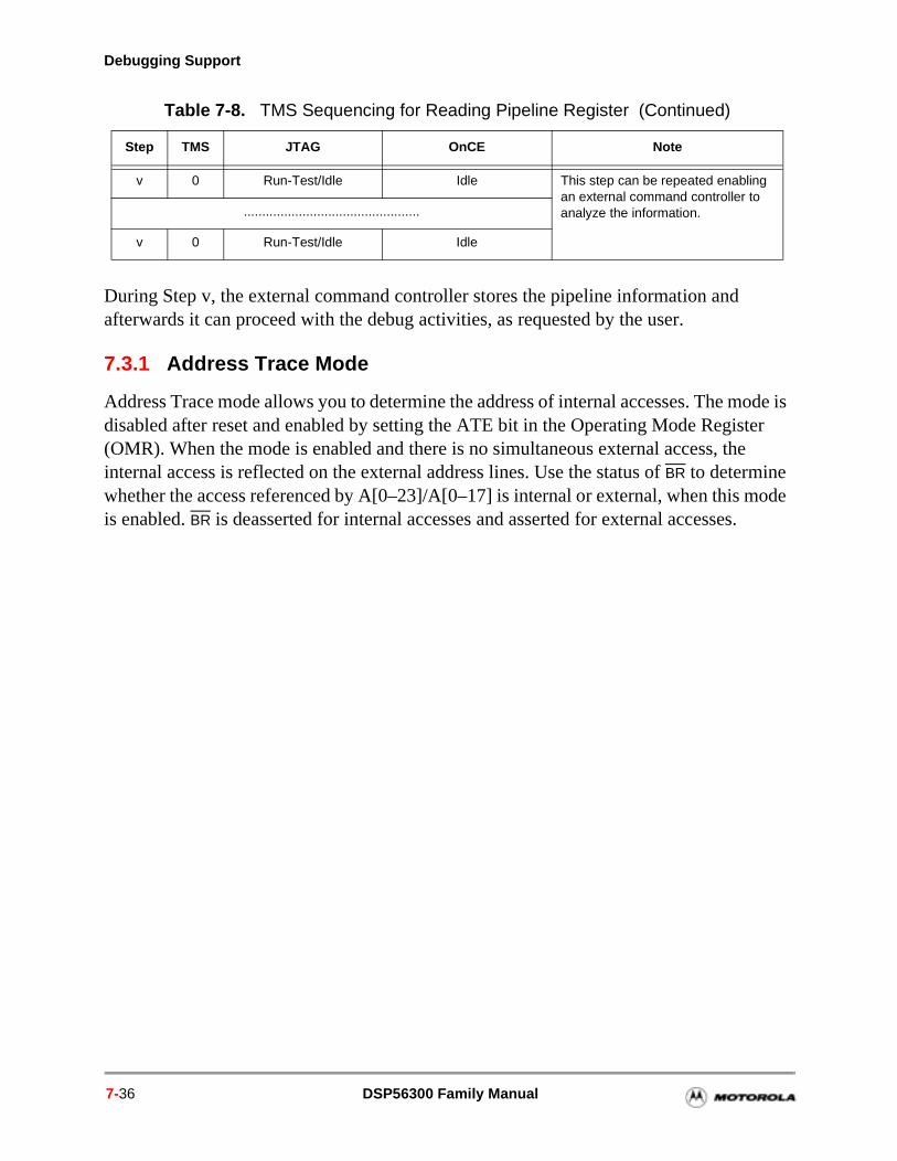
Debugging Support
mode .
During Step v, the external command controller stores the pipeline information and afterwards it can proceed with the debug activities, as requested by the user.
7.3.1 Address Trace Mode
Address Trace mode allows you to determine the address of internal accesses. The mode is disabled after reset and enabled by setting the ATE bit in the Operating Mode Register (OMR). When the mode is enabled and there is no simultaneous external access, the internal access is reflected on the external address lines. Use the status of BR to determine whether the access referenced by A[0–23]/A[0–17] is internal or external, when this is enabled. BR is deasserted for internal accesses and asserted for external accesses
v 0 Run-Test/Idle Idle This step can be repeated enabling an external command controller to analyze the information.................................................
v 0 Run-Test/Idle Idle
Table 7-8. TMS Sequencing for Reading Pipeline Register (Continued)
Step TMS JTAG OnCE Note
7-36 DSP56300 Family Manual
Chapter 8Instruction Cache
The instruction cache acts as a buffer memory between external memory and the DSP core processor. When code executes, the code words at the locations requested by the instruction set are copied into the instruction cache for direct access by the core processor. If the same code is used frequently in a set of program instructions, storage of these instructions in the cache yields an increase in throughput because external bus accesses are eliminated. In the DSP56300 instruction set are specific cache instructions that permit you to lock sectors of the cache and to flush the cache contents under software control. When enabled, the instruction cache comprises 1024 24-bit words (1 K words) of program memory that is not accessible to the user. The address space used by the instruction cache in internal program memory is reallocated to external program memory when the instruction cache is enabled. The enabled instruction cache has the following features:
Software-controlled Cache Enable (CE) bit in the Extended Mode Register (EMR) in the Status Register (SR)1
Eight-way, fully associative instruction cache with sectored placement policy
1- to 4-word transfer granularity
Least Recently Used (LRU) sector replacement algorithm
Transparent operation (that is, no user management is required)
Individual sector locking/unlocking
Global cache flush controlled by software
Cache controller status observable via the JTAG/OnCE port
Note: Supported instruction cache size is device-dependent. Refer to the device-specific technical data sheet to determine the instruction cache size for a device.
1. For details on the Status Register (SR), see Section 5.4.1.2, Status Register (SR).
DSP56300 Family Manual 8-1
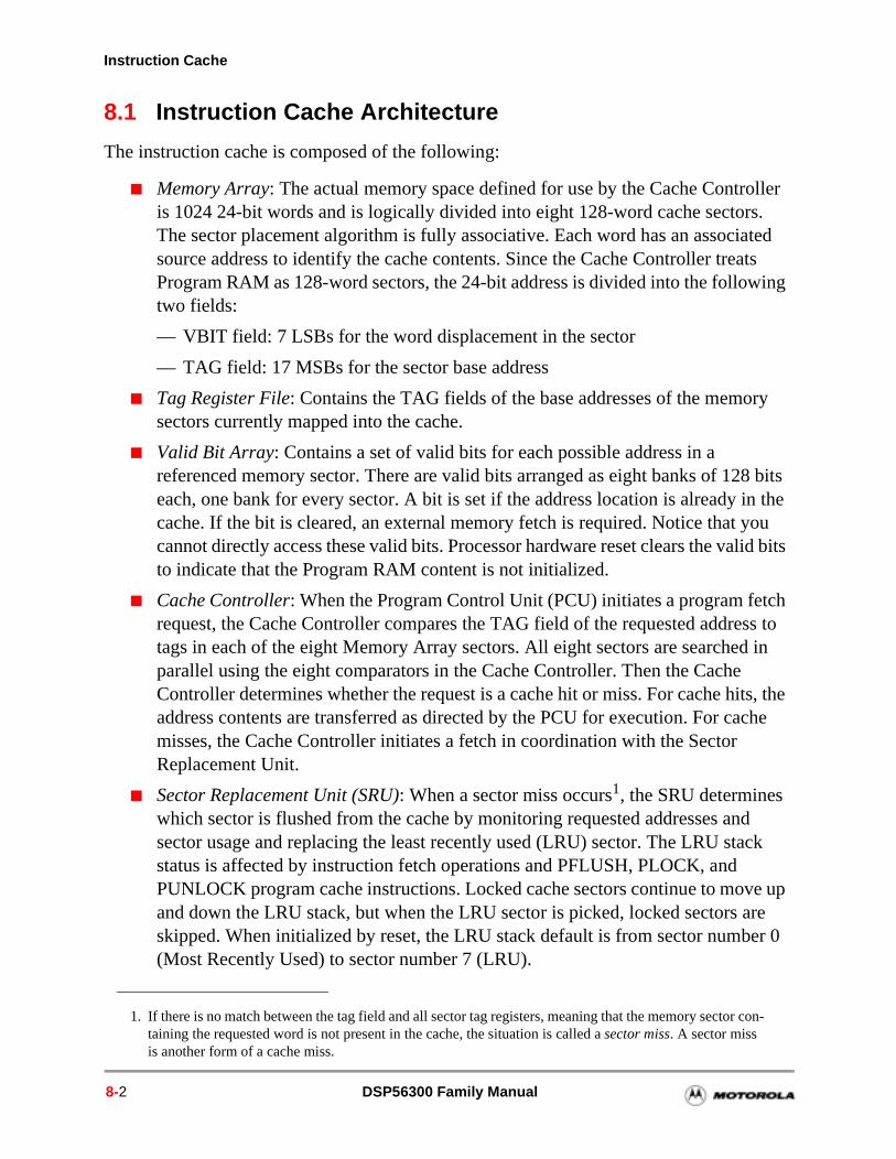
Instruction Cache
ry
8 bits in the ou lid bits
ch ss to in
ts, the che
d ck
e up re
er 0
8.1 Instruction Cache Architecture
The instruction cache is composed of the following:
Memory Array: The actual memory space defined for use by the Cache Controller is 1024 24-bit words and is logically divided into eight 128-word cache sectors. The sector placement algorithm is fully associative. Each word has an associated source address to identify the cache contents. Since the Cache Controller treats Program RAM as 128-word sectors, the 24-bit address is divided into the following two fields:
— VBIT field: 7 LSBs for the word displacement in the sector
— TAG field: 17 MSBs for the sector base address
Tag Register File: Contains the TAG fields of the base addresses of the memosectors currently mapped into the cache.
Valid Bit Array: Contains a set of valid bits for each possible address in a referenced memory sector. There are valid bits arranged as eight banks of 12each, one bank for every sector. A bit is set if the address location is already cache. If the bit is cleared, an external memory fetch is required. Notice that ycannot directly access these valid bits. Processor hardware reset clears the vato indicate that the Program RAM content is not initialized.
Cache Controller: When the Program Control Unit (PCU) initiates a program fetrequest, the Cache Controller compares the TAG field of the requested addretags in each of the eight Memory Array sectors. All eight sectors are searchedparallel using the eight comparators in the Cache Controller. Then the CacheController determines whether the request is a cache hit or miss. For cache hiaddress contents are transferred as directed by the PCU for execution. For camisses, the Cache Controller initiates a fetch in coordination with the Sector Replacement Unit.
Sector Replacement Unit (SRU): When a sector miss occurs1, the SRU determines which sector is flushed from the cache by monitoring requested addresses ansector usage and replacing the least recently used (LRU) sector. The LRU stastatus is affected by instruction fetch operations and PFLUSH, PLOCK, and PUNLOCK program cache instructions. Locked cache sectors continue to movand down the LRU stack, but when the LRU sector is picked, locked sectors askipped. When initialized by reset, the LRU stack default is from sector numb(Most Recently Used) to sector number 7 (LRU).
1. If there is no match between the tag field and all sector tag registers, meaning that the memory sector con-taining the requested word is not present in the cache, the situation is called a sector miss. A sector miss is another form of a cache miss.
8-2 DSP56300 Family Manual
Cache Programming Model
Figure 8-1 shows a block diagram of the instruction cache.
8.2 Cache Programming Model
The instruction cache is controlled by two control bits:
Cache Enable (CE) bit in the Extended Mode Register (EMR) part of the Status Register (SR Bit 19)
When CE is cleared, the instruction cache is disabled. When CE is set, the instruction cache is enabled.
Burst Enable (BE) bit in the Extended Operating Mode (EOM) part of the Operating Mode Register (OMR Bit 10)
When BE is cleared, the instruction cache transfer on a miss is one word. When BE is set, the instruction cache transfer on a miss increases to a burst block of one to four words.
Note: To ensure proper operation, do not clear the Cache Enable mode (CE bit in SR) while Burst mode is enabled (BE bit in OMR is set). Refer to Chapter 5, Program Control Unit, for details on the SR and OMR.
Figure 8-1. Instruction Cache Block Diagram
24-bit Program Address
Tag Register/Comparator 0
Hit/Miss
Instruction Word 0v0Instruction Word 1v1
Instruction Word 127/255v127/255
TAG Field 17 MSBs (for 1 K words cache)
VBIT Field7 LSBs (for 1 K words cache)
Instruction Cache 8-3
Instruction Cache
n che
rates.
mpares
that the the hit,
sent tor as
word read e
ent ction
t word
The instruction set supports the instruction cache via the following instructions:
— PLOCK
— PLOCKR
— PUNLOCK
— PUNLOCKR
— PFREE
— PFLUSH
— PFLUSHUN
8.2.1 Cache Operation
When enabled, the cache is involved in every instruction fetch. Its actions depend oseveral conditions, including whether the program address is (cache hit) or is not (camiss) in the instruction cache and whether Burst mode is enabled or disabled. The following paragraphs describe the conditions under which the instruction cache ope
8.2.1.1 Program Fetch
When the core generates an address for an instruction fetch, the cache controller coits TAG field to the tag values currently stored in the Tag Register File.
8.2.1.2 Cache Hit
If a tag match (that is, sector hit) exists, then the valid bit of the corresponding word incache sector is checked using the VBIT field as an address to the Valid Bit Array. If valid bit is set, meaning the word in the cache is valid, then that word is fetched fromcache location corresponding to the desired address. This situation is called a cachemeaning that both corresponding sector and corresponding instruction word are preand valid in the instruction cache. The Sector Replacement Unit (SRU) flags the secthe Most Recently Used (MRU).
8.2.1.3 Cache Word Miss When Burst Mode Is Disabled
If a tag match (that is, sector hit) exists, and Burst Mode is disabled, but the desiredis not flagged as valid (corresponding valid bit is cleared), then the cache initiates a access to the external program memory, introducing wait states into the pipeline. Thnumber of wait states is the number of wait states programmed into the Bus Controlregisters (BCRs) plus one, reflecting the type of memory used. The Sector ReplacemUnit (SRU) flags the sector as the Most Recently Used (MRU), and the fetched instruis sent to the core and copied to the relevant sector location. Then the valid bit of thais set.
8-4 DSP56300 Family Manual
Cache Programming Model
8.2.1.4 Cache Word Miss When Burst Mode Is Enabled
If a tag match (that is, sector hit) exists, and Burst Mode is enabled, but the desired word is not flagged as valid (that is, the corresponding valid bit is cleared), then the cache initiates a burst of up to four read accesses to the external program memory. The exact number of fetch requests depends on the value of the two LSBs of the address of the initiating fetch that was detected as a miss, as indicated in Table 8-1.
These external read accesses introduce wait states into the pipeline. The number of wait states for each fetch is the number of wait states that are programmed into the bus control registers (BCRs) plus one, reflecting the type of memory used. The Sector Replacement Unit (SRU) flags the sector as the Most Recently Used (MRU), and each of the fetched instructions is copied to the relevant sector location. Then the valid bit of that word is set.
8.2.1.5 Sector Miss
If there is no match between the TAG field and all sector Tag registers, meaning that the memory sector containing the requested word is not in the cache, the situation is called a sector miss, which is another form of a cache miss. If a sector miss occurs, the SRU selects the sector to be replaced. The cache controller then flushes the selected cache sector by clearing all corresponding valid bits, loads the corresponding Tag register with the new TAG field, and simultaneously initiates an access to the external Program RAM, as described in Section 8.2.1.3 and Section 8.2.1.4. The sector is flagged as MRU, the fetched instruction is sent to the core and copied to the relevant sector location, and the valid bit of that word is set.
Table 8-1. Determining the Number of Required Fetches in Burst Mode
Value of the 2 LSBs of the Requested
Address
Number of Fetch Requests Initiated
00 Four requests are initiated
01 Three requests are initiated
10 Two requests are initiated
11 Only one request is initiated (that is, same as if the Burst mode is disabled)
Instruction Cache 8-5
Instruction Cache
che
ro).
ry. this k). A
The
ctor sector. is
d. The es not ents.
d
f the
.
ory y in a
lready
8.2.2 Default Mode After Hardware Reset
After hardware reset, the instruction cache is disabled. The cache is initialized as follows:
All valid bits are cleared.
All Tag Registers are initialized to ‘all ones,’ that is, $1FFFF for a 1 K words ca(17-bit Tag Register).
The LRU stack holds a default descending order of sectors (from seven to ze
All cache sectors are in the unlocked state.
8.3 Cache Locking
Cache locking is useful for locking some time-critical code parts in the cache memoWhen a cache sector is locked, the Sector Replacement Unit (SRU) cannot replacesector, even if it becomes the Least Recently Used (LRU) sector (bottom of LRU stacsector can be locked by the instructions PLOCK or PLOCKR. The operand for theseinstructions is an effective memory address (absolute or program counter-relative). cache sector to which this address belongs, if one exists, is locked. If the specified effective address does not belong to one of the current cache sectors, a memory secontaining this address is allocated into the cache, thereby replacing the LRU cache This cache sector is locked, but empty. If all the cache sectors are already locked, thmemory sector is not allocated into the cache, and the lock operation is not executelocked cache sector becomes MRU. Locking a cache sector already in the cache doaffect its contents, the value of its valid bits, or the corresponding Tag Register cont
Note: PLOCK and PLOCKR are detected as illegal opcodes when the instructioncache is not enabled. Issuing these instructions when the cache is disableinitiates the Illegal Interrupt. A distance of at least 3 instruction cycles (equivalent to three NOP instructions) should be maintained between an instruction that changes the value of the Cache Enable bit (CE) and one oinstructions PLOCK and PLOCKR.
8.4 Cache Unlocking
A locked sector can be unlocked to allow sector replacement from that cache sectorUnlocking can be performed in three different ways.
A locked sector is unlocked by the PFREE, PUNLOCK, or PUNLOCKR instructions. The operands of the PUNLOCK and PUNLOCKR instructions areeffective memory addresses (absolute or program counter-relative). The memsector containing this address is allocated into a cache sector, if it is not alreadcache sector, and this cache sector is unlocked. If all the cache sectors are a
8-6 DSP56300 Family Manual
Flushing the Cache
the is
n n an
f the
reset
che
e
locked, this memory sector is not allocated into the cache, and the unlock operation is not executed. The unlocked cache sector becomes MRU and is enabled for replacement by the LRU algorithm. Unlocking a locked cache sector using these instructions does not affect its contents, its tag, or its valid bits.
All locked sectors are unlocked simultaneously using the instruction PFREE, which allows you to reset the locking mechanism. Unlocking the sectors using PFREE neither affects the sector contents (instructions already fetched into the sector storage area), valid bits, tags, nor the LRU stack status.
The locked sectors are unlocked by the PFLUSH instruction. Unlocking the sectors via PFLUSH clears all the sectors’ valid bits and sets the LRU stack and Tag registers to their default values.
Note: PFREE, PUNLOCK and PUNLOCKR are detected as illegal opcodes wheninstruction cache is not enabled. Issuing these instructions when the cachedisabled initiates the Illegal Interrupt. A distance of at least three instructiocycles (equivalent to three NOP instructions) should be maintained betweeinstruction that changes the value of the Cache Enable bit (CE) and one oinstructions PFREE, PUNLOCK and PUNLOCKR.
8.5 Flushing the Cache
Executing the PFLUSH or PFLUSHUN instructions flushes the cache. Executing PFLUSH causes a global cache flush that brings the cache to the following hardwareinitial condition:
All valid bits are cleared.
All Tag Registers are initialized to ‘all ones,’ that is, $1FFFF for a 1 K words ca(17-bit Tag Register).
The LRU stack holds a default descending order of sectors (from 7 to 0).
All cache sectors are in the unlocked state.
Executing PFLUSHUN causes a flush only to the unlocked sectors and initializes thcache as follows:
All valid bits of the unlocked sectors are cleared.
All Tag Registers of the unlocked sectors are initialized to ‘all ones,’ that is, $1FFFF for a 1 K words cache (17-bit Tag Register).
The LRU stack holds a default descending order of sectors (from 7 to 0).
Instruction Cache 8-7
Instruction Cache
e not
ory
of the ce
Note: Coherency between Program RAM mode and Cache mode is not supported by the instruction cache Controller. It is not possible to fill the cache while in Program RAM mode and use the contents after switching to Cache mode. The cache is automatically flushed when switching from Cache to Program RAM mode.
Note: PFLUSH and PFLUSHUN are detected as illegal opcodes when the instruction cache is not enabled. Issuing these instructions when the cache is disabled initiates the Illegal Interrupt. At least three instruction cycles (equivalent to three NOP instructions) should be maintained between an instruction that changes the value of the Cache Enable bit (CE) and one of the instructions PFLUSH and PFLUSHUN.
8.6 Data Transfers to/from Instruction Cache
Data transfers to/from the program memory can be accomplished by the DMA or by software, using MOVE instructions. Only PMOVE instructions can transfer data to/from the instruction cache.
8.6.1 DMA Transfers
DMA transfers have no effect on the Tag Register File, Valid Bit Array and LRU Stack, even when the cache is enabled. When the cache is disabled, the instruction cache memory space is considered part of the internal program memory space. DMA transfers to/from this space execute without any limitation. When the cache is enabled, the instruction cache memory space is considered part of the external program memory space. DMA transfers to/from this space execute through the external memory expansion port. Coherency between the external program memory and the contents of the instruction cache is not maintained.
8.6.2 Software-Controlled Transfers
The term “PMOVE” indicates use of a MOVE instruction to transfer data between thprogram memory space and any other source/destination. PMOVE data transfers doaffect the Tag Register File and LRU Stack, even if the cache is enabled. The term “PMOVEW” indicates a PMOVE transfer with the program memory space as the destination. The term “PMOVER” indicates a PMOVE transfer with the program memspace as the source.
When the cache is disabled, the instruction cache memory space is considered partinternal program memory space. PMOVER from this space or PMOVEW to this spa
8-8 DSP56300 Family Manual
Using the Instruction Cache in Real-Time Applications
execute without any limitation. When the cache is enabled, the cache controller checks the PMOVER transfers for a hit or miss:
If the cache controller generates a hit on the program memory space address, the data is read from the cache memory array. Since PMOVE is not considered an instruction fetch operation, the LRU state is not changed by this transfer.
If the cache controller generates a miss on the program memory space address, the data is read from the external program memory. The Cache state is not changed by this transfer. In Burst mode, no burst is initiated. Be aware that the core is delayed by the number of wait states specified in the BCR.
When the cache is enabled, the cache controller checks the PMOVEW transfers for a hit or miss:
If the cache controller generates a sector hit on the program memory space address, the data is written both to the cache memory array and to the external program memory. The valid bit of the word is set. The LRU stack is not changed by this transfer. Be aware that the core is delayed by the number of wait states specified in the BCR.
If the cache controller generates a sector miss on the program memory space address, the data is written only to the external program memory. The Cache state is not changed by this transfer. In Burst mode, no burst is initiated. Be aware that the core is delayed by the number of wait states specified in the BCR.
Note: For proper operation, none of the three instructions before a PMOVE transfer should clear or set the Status Register CE bit.
8.7 Using the Instruction Cache in Real-Time Applications
The following tips help you to use the instruction cache in real-time applications:
Each sector (out of the 8, 128 words) can be individually locked.
Locking a sector prevents its replacement in case of a miss even if it would have been its turn to be replaced.
It is typical to lock the interrupt vector tables and routines to ensure the fastest response. Furthermore, these routines can be loaded beforehand using PMOVEs to ensure a hit on the first access.
The cache can be globally flushed (for example, for task switching) with one instruction.
The cache can be globally unlocked (that is any sector can be replaced in case of a miss) or any individual sector can be unlocked allowing its replacement.
Instruction Cache 8-9
Instruction Cache
The penalty incurred for a cache miss is identical with the one for a regular instruction fetch from external memory (1 wait state with 15 ns SRAM at 66 MHz).
The software simulator permits application tailoring since it provides clock exact behavior.
In general, an algorithm that requires N clocks to execute and is repeated M times, requires (WS is a number of wait states):
(N + N x WS)M = N x M(WS + 1) clocks.
In a cache environment, the same algorithm requires:
N(WS + 1) + N(M - 1) = N(M + WS) clocks.
8.8 Debugging Instruction Cache Operation
While the cache is enabled, full non-intrusive system debug capability in Debug mode includes being able to observe:
What memory sectors are currently mapped into cache
Which cache sectors are locked
Which cache sector is the LRU
When cache hits occur
Debug mode allows you to read the Tag register contents, lock bits, LRU bits, and hit-status serially from the OnCE module via the JTAG port. You can also read the valid bits of specific cache locations. To check whether an address with MSBs in a Tag register is in the cache, send the opcode of a MOVEM from this address. Bit 5 of the OnCE Status and Control register (OSCR) indicates the value of the valid bit. See Chapter 7, Debugging Support, for more information.
Note: Each read of the cache status via the OnCE module should occur only when the device is in the Debug mode and should access all nine registers, so that reads start with tag #0 every time.
8-10 DSP56300 Family Manual
ssible.
for
Chapter 9External Memory Interface (Port A)
The external memory expansion port, Port A, can be used either for memory expansion or for memory-mapped I/O. External memory is easily and quickly retrieved through the use of DMA or simple MOVE commands. For more information on Port A programming see application note AN1751D, DSP563xx Port A Programming. Several features make Port A versatile and easy to use, resulting in a low part-count connection with fast or slow static memories, dynamic memories, I/O devices and multiple bus master system. The Port A data bus is 24 bits wide with a separate 18-bit or 24-bit address bus.
External memory is divided into three possible 16 M × 24-bit spaces: X data, Y data, and program memory. Each space or all spaces can access a given external memory. Access type and attributes are under software control. See the memory map in Chapter 11,
Operating Modes and Memory Spaces, for memory space that is not accessible through Port A. An internal wait state generator can be programmed to statically insert up to 31 wait states for access to slower memory or I/O devices. A Transfer Acknowledge (TA) signal allows an external device to dynamically control the number of wait states inserted into a bus access operation. The bus arbitration allows multiple potential masters of the Port A bus. One DSP56300 processor can use the Port A bus to access external devices while other potential masters perform internal operations that do not require the Port A bus. See the memory map in the device-specific user’s manual for memory space that is not acce
9.1 Signal Description
Table 9-1 through Table 9-3 show the signals that the external memory interface usescontrolling and transferring data.
DSP56300 Family Manual 9-1
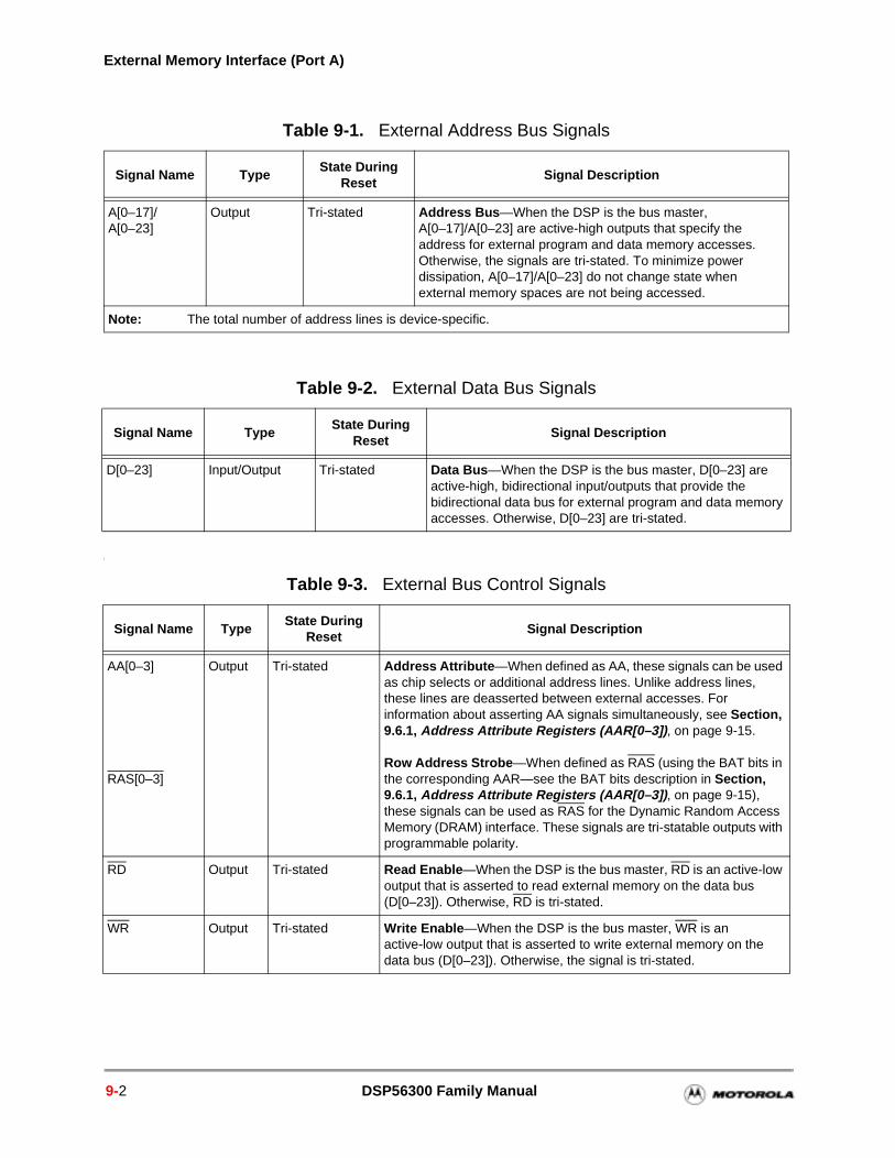
External Memory Interface (Port A)
l
Table 9-1. External Address Bus Signals
Signal Name TypeState During
ResetSignal Description
A[0–17]/A[0–23]
Output Tri-stated Address Bus—When the DSP is the bus master, A[0–17]/A[0–23] are active-high outputs that specify the address for external program and data memory accesses. Otherwise, the signals are tri-stated. To minimize power dissipation, A[0–17]/A[0–23] do not change state when external memory spaces are not being accessed.
Note: The total number of address lines is device-specific.
Table 9-2. External Data Bus Signals
Signal Name TypeState During
ResetSignal Description
D[0–23] Input/Output Tri-stated Data Bus—When the DSP is the bus master, D[0–23] are active-high, bidirectional input/outputs that provide the bidirectional data bus for external program and data memory accesses. Otherwise, D[0–23] are tri-stated.
Table 9-3. External Bus Control Signals
Signal Name TypeState During
ResetSignal Description
AA[0–3]
RAS[0–3]
Output Tri-stated Address Attribute—When defined as AA, these signals can be used as chip selects or additional address lines. Unlike address lines, these lines are deasserted between external accesses. For information about asserting AA signals simultaneously, see Section, 9.6.1, Address Attribute Registers (AAR[0–3]) , on page 9-15.
Row Address Strobe—When defined as RAS (using the BAT bits in the corresponding AAR—see the BAT bits description in Section, 9.6.1, Address Attribute Registers (AAR[0–3]) , on page 9-15), these signals can be used as RAS for the Dynamic Random Access Memory (DRAM) interface. These signals are tri-statable outputs with programmable polarity.
RD Output Tri-stated Read Enable—When the DSP is the bus master, RD is an active-low output that is asserted to read external memory on the data bus (D[0–23]). Otherwise, RD is tri-stated.
WR Output Tri-stated Write Enable—When the DSP is the bus master, WR is an active-low output that is asserted to write external memory on the data bus (D[0–23]). Otherwise, the signal is tri-stated.
9-2 DSP56300 Family Manual
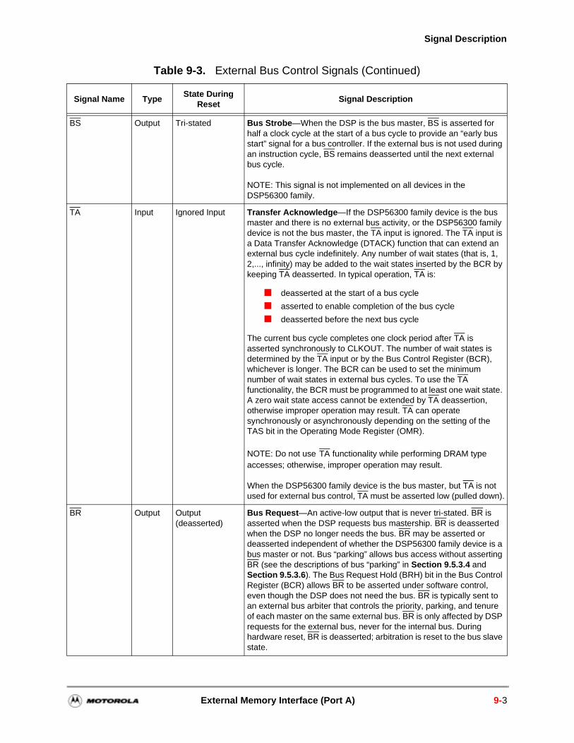
Signal Description
BS Output Tri-stated Bus Strobe—When the DSP is the bus master, BS is asserted for half a clock cycle at the start of a bus cycle to provide an “early bus start” signal for a bus controller. If the external bus is not used during an instruction cycle, BS remains deasserted until the next external bus cycle.
NOTE: This signal is not implemented on all devices in the DSP56300 family.
TA Input Ignored Input Transfer Acknowledge—If the DSP56300 family device is the bus master and there is no external bus activity, or the DSP56300 family device is not the bus master, the TA input is ignored. The TA input is a Data Transfer Acknowledge (DTACK) function that can extend an external bus cycle indefinitely. Any number of wait states (that is, 1, 2,..., infinity) may be added to the wait states inserted by the BCR by keeping TA deasserted. In typical operation, TA is:
deasserted at the start of a bus cycle
asserted to enable completion of the bus cycle
deasserted before the next bus cycle
The current bus cycle completes one clock period after TA is asserted synchronously to CLKOUT. The number of wait states is determined by the TA input or by the Bus Control Register (BCR), whichever is longer. The BCR can be used to set the minimum number of wait states in external bus cycles. To use the TA functionality, the BCR must be programmed to at least one wait state. A zero wait state access cannot be extended by TA deassertion, otherwise improper operation may result. TA can operate synchronously or asynchronously depending on the setting of the TAS bit in the Operating Mode Register (OMR).
NOTE: Do not use TA functionality while performing DRAM type accesses; otherwise, improper operation may result.
When the DSP56300 family device is the bus master, but TA is not used for external bus control, TA must be asserted low (pulled down).
BR Output Output(deasserted)
Bus Request—An active-low output that is never tri-stated. BR is asserted when the DSP requests bus mastership. BR is deasserted when the DSP no longer needs the bus. BR may be asserted or deasserted independent of whether the DSP56300 family device is a bus master or not. Bus “parking” allows bus access without asserting BR (see the descriptions of bus “parking” in Section 9.5.3.4 and Section 9.5.3.6). The Bus Request Hold (BRH) bit in the Bus Control Register (BCR) allows BR to be asserted under software control, even though the DSP does not need the bus. BR is typically sent to an external bus arbiter that controls the priority, parking, and tenure of each master on the same external bus. BR is only affected by DSP requests for the external bus, never for the internal bus. During hardware reset, BR is deasserted; arbitration is reset to the bus slave state.
Table 9-3. External Bus Control Signals (Continued)
Signal Name TypeState During
ResetSignal Description
External Memory Interface (Port A) 9-3
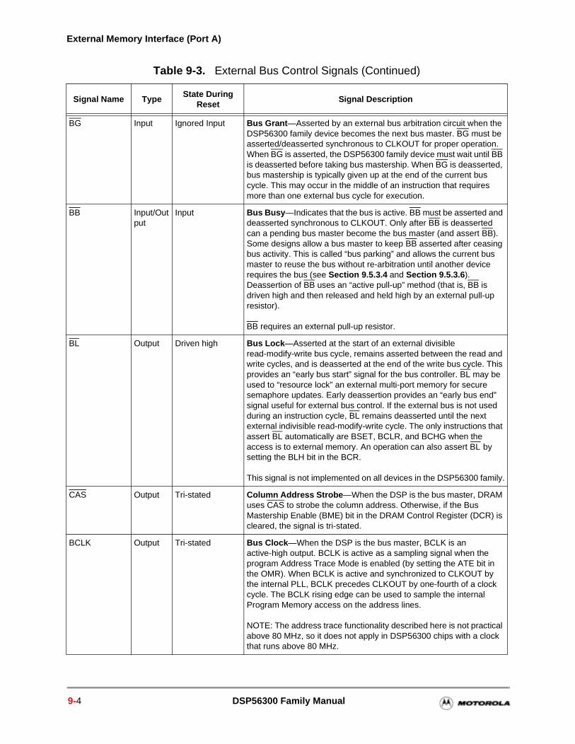
External Memory Interface (Port A)
BG Input Ignored Input Bus Grant—Asserted by an external bus arbitration circuit when the DSP56300 family device becomes the next bus master. BG must be asserted/deasserted synchronous to CLKOUT for proper operation. When BG is asserted, the DSP56300 family device must wait until BB is deasserted before taking bus mastership. When BG is deasserted, bus mastership is typically given up at the end of the current bus cycle. This may occur in the middle of an instruction that requires more than one external bus cycle for execution.
BB Input/Output
Input Bus Busy—Indicates that the bus is active. BB must be asserted and deasserted synchronous to CLKOUT. Only after BB is deasserted can a pending bus master become the bus master (and assert BB). Some designs allow a bus master to keep BB asserted after ceasing bus activity. This is called “bus parking” and allows the current bus master to reuse the bus without re-arbitration until another device requires the bus (see Section 9.5.3.4 and Section 9.5.3.6). Deassertion of BB uses an “active pull-up” method (that is, BB is driven high and then released and held high by an external pull-up resistor).
BB requires an external pull-up resistor.
BL Output Driven high Bus Lock—Asserted at the start of an external divisible read-modify-write bus cycle, remains asserted between the read and write cycles, and is deasserted at the end of the write bus cycle. This provides an “early bus start” signal for the bus controller. BL may be used to “resource lock” an external multi-port memory for secure semaphore updates. Early deassertion provides an “early bus end” signal useful for external bus control. If the external bus is not used during an instruction cycle, BL remains deasserted until the next external indivisible read-modify-write cycle. The only instructions that assert BL automatically are BSET, BCLR, and BCHG when the access is to external memory. An operation can also assert BL by setting the BLH bit in the BCR.
This signal is not implemented on all devices in the DSP56300 family.
CAS Output Tri-stated Column Address Strobe—When the DSP is the bus master, DRAM uses CAS to strobe the column address. Otherwise, if the Bus Mastership Enable (BME) bit in the DRAM Control Register (DCR) is cleared, the signal is tri-stated.
BCLK Output Tri-stated Bus Clock—When the DSP is the bus master, BCLK is an active-high output. BCLK is active as a sampling signal when the program Address Trace Mode is enabled (by setting the ATE bit in the OMR). When BCLK is active and synchronized to CLKOUT by the internal PLL, BCLK precedes CLKOUT by one-fourth of a clock cycle. The BCLK rising edge can be used to sample the internal Program Memory access on the address lines.
NOTE: The address trace functionality described here is not practical above 80 MHz, so it does not apply in DSP56300 chips with a clock that runs above 80 MHz.
Table 9-3. External Bus Control Signals (Continued)
Signal Name TypeState During
ResetSignal Description
9-4 DSP56300 Family Manual
Port Operation
9.2 Port Operation
External bus timing is defined by the operation of the Address Bus, Data Bus, and Bus Control pins as described in the previous sections. The DSP56300 core external ports interface with a wide variety of memory and peripheral devices, high speed SRAMs and DRAMs, and slower memory devices. The TA control signal and the Bus Control Register (BCR) described in Section 9.6.2 control the external bus timing. The BCR provides constant bus access timing through the insertion of wait states. TA provides dynamic bus access timing. The number of wait states for each external access is determined by the TA input or by the BCR, whichever specifies the longest time.
9.2.1 External Memory Addressing
The external memory address is defined by the Address Bus (A[0–17]/A[0–23]) and the memory Address Attribute signals (AA[0–3]). The AA signals can operate as memory-mapped chip selects or address lines to external devices, depending on the mode selected. The AA signals have the same timing as the Address Bus signals and can be used as additional address lines. The AA signals are also used to generate Chip Select (CS) signals for the appropriate memory chips. These CS signals change the memory chips from low power Standby mode to Active mode and begin the access time. This allows slower memories to be used since the AA signals are address-based rather than read or write enable-based.
For DSP56300 parts with 18 address lines, the AA signals can be used to extend memory access, if used as upper addressing bits. If all four AA signals are used as address lines, the total addressable external memory can be 4 M × 24-bit if the OMR[APD] bit is set. When the APD bit is set, it disables the priority assigned to AA[0–3] thereby enabling more than one AA signal to be active simultaneously. Additionally, if all four AA signals are used as address lines, then the memory must always be selected, because no AA signals are available for chip select. As a result, an external read or write outside the 4 M range could still go to the external memory (depending on the settings of the AA registers). Be aware that unlike standard address bus lines, AA[0–3] do not hold their state after a read or write operation.
BCLK Output Tri-stated Bus Clock—When the DSP is the bus master, BCLK is an active-low output that is the inverse of the BCLK signal. Otherwise, the signal is tri-stated.
Table 9-3. External Bus Control Signals (Continued)
Signal Name TypeState During
ResetSignal Description
External Memory Interface (Port A) 9-5
External Memory Interface (Port A)
9.2.2 SRAM Support
The DSP56300 core can interface easily with SRAMs. Because the address must remain stable during the entire bus cycle, however, at least one wait state must be inserted regardless of the speed of the SRAM. Figure 9-1 shows an SRAM access timing example (for detailed timing information, see the specific technical data sheet for the device used in the design). Figure 9-2 shows a typical DSP56300 family device-to-SRAM connection.
SRAM access consists of the following steps:
1. Address Bus (A[0–17]/A[0–23]), Address Attributes (AA[0–3), and Bus Strobe (BS) are asserted in the middle of CLKOUT high phase.
2. Write enable (WR) is asserted with the falling edge of CLKOUT (for a single wait state access). Read enable (RD) is asserted in the middle of CLKOUT low phase.
3. For a write operation, data is driven in the middle of CLKOUT high phase. For a read operation, data is sampled in the middle of CLKOUT last low phase of the external access.
For accessing slower memories, wait states (from the BCR or by the TA signal) postpone the disappearance of the external address and increase memory access time. In any case, SRAM access requires at least one wait state—that is, above 100 MHz SRAM access requires two wait states.
9-6 DSP56300 Family Manual
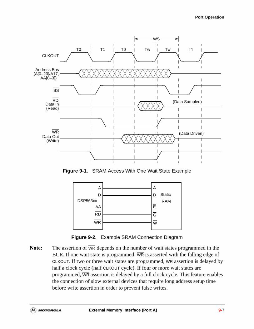
Port Operation
Note: The assertion of WR depends on the number of wait states programmed in the BCR. If one wait state is programmed, WR is asserted with the falling edge of CLKOUT. If two or three wait states are programmed, WR assertion is delayed by half a clock cycle (half CLKOUT cycle). If four or more wait states are programmed, WR assertion is delayed by a full clock cycle. This feature enables the connection of slow external devices that require long address setup time before write assertion in order to prevent false writes.
Figure 9-1. SRAM Access With One Wait State Example
Figure 9-2. Example SRAM Connection Diagram
CLKOUT
Address Bus
Data Out
(Data Sampled)
T0 T1 T0 Tw Tw T1
WS
BS
WR
RD
(A[0–23]/A17,AA[0–3])
Data In
(Write)
(Read)
(Data Driven)
DSP563xx
Static
RAM
A
D
A
D
AA
RD
WR
E
G
W
External Memory Interface (Port A) 9-7
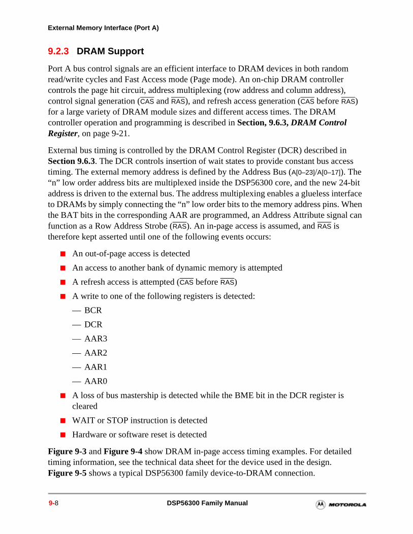
External Memory Interface (Port A)
4-bit terface hen l can
9.2.3 DRAM Support
Port A bus control signals are an efficient interface to DRAM devices in both random read/write cycles and Fast Access mode (Page mode). An on-chip DRAM controller controls the page hit circuit, address multiplexing (row address and column address), control signal generation (CAS and RAS), and refresh access generation (CAS before RAS) for a large variety of DRAM module sizes and different access times. The DRAM controller operation and programming is described in Section, 9.6.3, DRAM Control Register, on page 9-21.
External bus timing is controlled by the DRAM Control Register (DCR) described in Section 9.6.3. The DCR controls insertion of wait states to provide constant bus access timing. The external memory address is defined by the Address Bus (A[0–23]/A[0–17]). The “n” low order address bits are multiplexed inside the DSP56300 core, and the new 2address is driven to the external bus. The address multiplexing enables a glueless into DRAMs by simply connecting the “n” low order bits to the memory address pins. Wthe BAT bits in the corresponding AAR are programmed, an Address Attribute signafunction as a Row Address Strobe (RAS). An in-page access is assumed, and RAS is therefore kept asserted until one of the following events occurs:
An out-of-page access is detected
An access to another bank of dynamic memory is attempted
A refresh access is attempted (CAS before RAS)
A write to one of the following registers is detected:
— BCR
— DCR
— AAR3
— AAR2
— AAR1
— AAR0
A loss of bus mastership is detected while the BME bit in the DCR register is cleared
WAIT or STOP instruction is detected
Hardware or software reset is detected
Figure 9-3 and Figure 9-4 show DRAM in-page access timing examples. For detailedtiming information, see the technical data sheet for the device used in the design. Figure 9-5 shows a typical DSP56300 family device-to-DRAM connection.
9-8 DSP56300 Family Manual
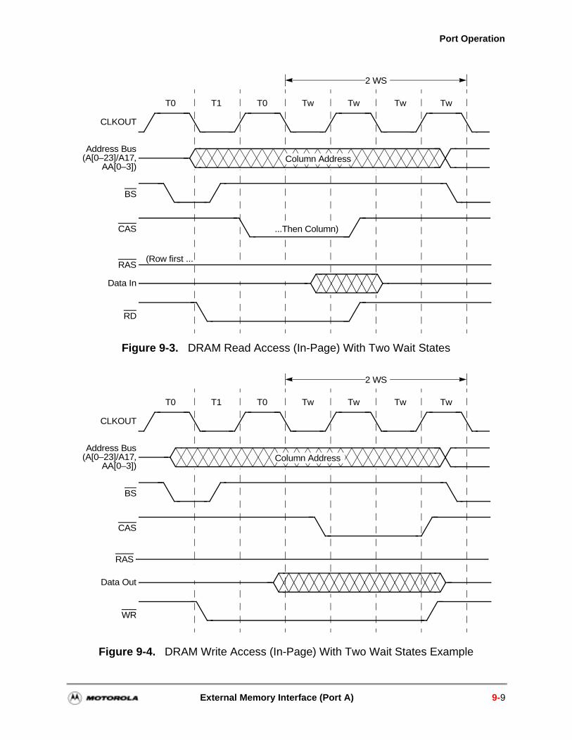
Port Operation
Figure 9-3. DRAM Read Access (In-Page) With Two Wait States
Figure 9-4. DRAM Write Access (In-Page) With Two Wait States Example
CLKOUT
Data In
BS
RD
CAS
RAS
Address Bus(A[0–23]/A17,
AA[0–3])
T0 T1 T0 Tw Tw Tw
2 WS
Tw
(Row first ...
...Then Column)
Column Address
CLKOUT
Data Out
BS
WR
CAS
Address Bus(A[0–23]/A17,
AA[0–3])
T0 T1 T0 Tw Tw Tw
2 WS
Tw
Column Address
RAS
External Memory Interface (Port A) 9-9
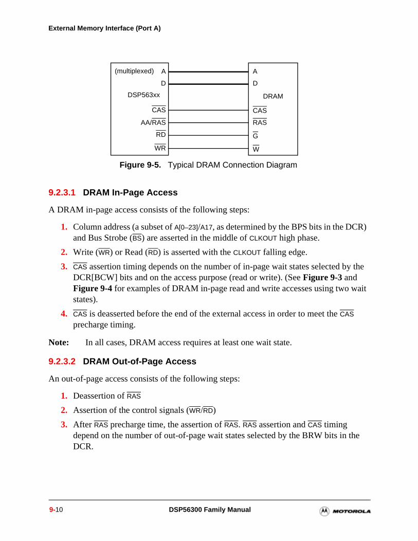
External Memory Interface (Port A)
9.2.3.1 DRAM In-Page Access
A DRAM in-page access consists of the following steps:
1. Column address (a subset of A[0–23]/A17, as determined by the BPS bits in the DCR) and Bus Strobe (BS) are asserted in the middle of CLKOUT high phase.
2. Write (WR) or Read (RD) is asserted with the CLKOUT falling edge.
3. CAS assertion timing depends on the number of in-page wait states selected by the DCR[BCW] bits and on the access purpose (read or write). (See Figure 9-3 and Figure 9-4 for examples of DRAM in-page read and write accesses using two wait states).
4. CAS is deasserted before the end of the external access in order to meet the CAS precharge timing.
Note: In all cases, DRAM access requires at least one wait state.
9.2.3.2 DRAM Out-of-Page Access
An out-of-page access consists of the following steps:
1. Deassertion of RAS
2. Assertion of the control signals (WR/RD)
3. After RAS precharge time, the assertion of RAS. RAS assertion and CAS timing depend on the number of out-of-page wait states selected by the BRW bits in the DCR.
Figure 9-5. Typical DRAM Connection Diagram
DSP563xx DRAM
A
D
A
D
AA/RAS
RD
WR
RAS
G
W
CAS CAS
(multiplexed)
9-10 DSP56300 Family Manual
Bus Arbitration Signals
ny
hich ndent
vices riety
erted
ting t
by
9.3 Port A Disable
In applications sensitive to power consumption, Port A may not be required because the memory that is used resides in the processor. A special feature of the Port A controller allows you to reduce the power consumption significantly by setting the EBD bit in the Operating Mode Register (OMR) to disable the Port A controller. This causes the DSP56300 device to release the bus (that is, deassert BR and BL, tri-state BB, and ignore BG). With the controller disabled, no external DMA accesses or refresh accesses can be performed.
Note: To prevent improper operation when OMR[EBD] is set, do not access external memory, and always clear Refresh Enable (BREN—DCR[13]) to prevent aexternal DRAM refresh attempts.
9.4 Bus Handshake and Arbitration
Bus transactions are governed by a single bus master. Bus arbitration determines wdevice becomes the bus master. The arbitration logic implementation is system-depebut must result in, at most, one device becoming the bus master (even if multiple derequest bus ownership). The arbitration signals permit simple implementation of a vaof bus arbitration schemes (for example, fairness, priority, and so on). The system designer must provide the external logic to implement the arbitration scheme.
9.5 Bus Arbitration Signals
There are three bus arbitration signals. Two of them (BR and BG) are local arbitration signals between a potential bus master and the arbitration logic; BB is a system arbitration signal:
Bus Request (BR)—Asserted by a device to request use of the bus; it is held assuntil the device no longer needs the bus. This includes time when it is the busmaster as well as when it is not the bus master.
Bus Grant (BG)—Asserted by the bus arbitration controller to signal the requesdevice that it is the bus master elect, BG is valid only when the bus is not busy (thais, BB is not asserted).
Bus Busy (BB)—This signal is driven by the current bus master and controls thehand-over of bus ownership by the bus master at the end of bus possession. BB is an active pull-up signal (that is, it is driven high before release and then held highan external pull-up resistor).
External Memory Interface (Port A) 9-11
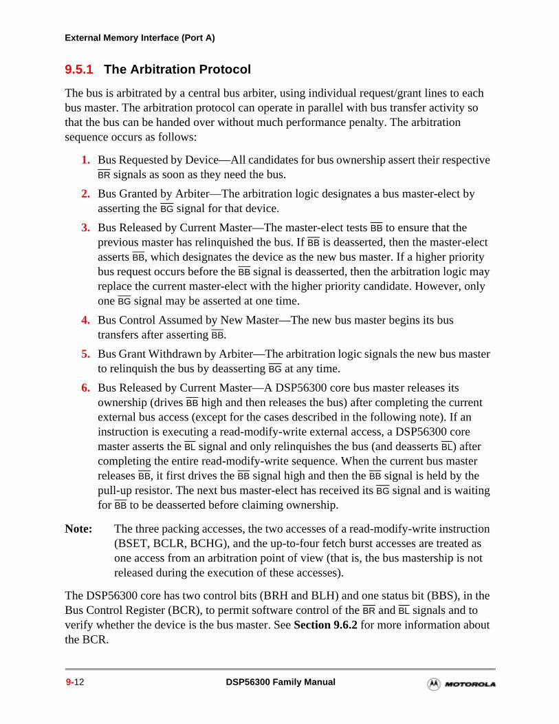
External Memory Interface (Port A)
ive
y
ct rity ay nly
ster
nt n
e
ter
ction as not
n the
9.5.1 The Arbitration Protocol
The bus is arbitrated by a central bus arbiter, using individual request/grant lines to each bus master. The arbitration protocol can operate in parallel with bus transfer activity so that the bus can be handed over without much performance penalty. The arbitration sequence occurs as follows:
1. Bus Requested by Device—All candidates for bus ownership assert their respectBR signals as soon as they need the bus.
2. Bus Granted by Arbiter—The arbitration logic designates a bus master-elect basserting the BG signal for that device.
3. Bus Released by Current Master—The master-elect tests BB to ensure that the previous master has relinquished the bus. If BB is deasserted, then the master-eleasserts BB, which designates the device as the new bus master. If a higher priobus request occurs before the BB signal is deasserted, then the arbitration logic mreplace the current master-elect with the higher priority candidate. However, oone BG signal may be asserted at one time.
4. Bus Control Assumed by New Master—The new bus master begins its bus transfers after asserting BB.
5. Bus Grant Withdrawn by Arbiter—The arbitration logic signals the new bus mato relinquish the bus by deasserting BG at any time.
6. Bus Released by Current Master—A DSP56300 core bus master releases itsownership (drives BB high and then releases the bus) after completing the curreexternal bus access (except for the cases described in the following note). If ainstruction is executing a read-modify-write external access, a DSP56300 cormaster asserts the BL signal and only relinquishes the bus (and deasserts BL) after completing the entire read-modify-write sequence. When the current bus masreleases BB, it first drives the BB signal high and then the BB signal is held by the pull-up resistor. The next bus master-elect has received its BG signal and is waiting for BB to be deasserted before claiming ownership.
Note: The three packing accesses, the two accesses of a read-modify-write instru(BSET, BCLR, BCHG), and the up-to-four fetch burst accesses are treatedone access from an arbitration point of view (that is, the bus mastership is released during the execution of these accesses).
The DSP56300 core has two control bits (BRH and BLH) and one status bit (BBS), iBus Control Register (BCR), to permit software control of the BR and BL signals and to verify whether the device is the bus master. See Section 9.6.2 for more information about the BCR.
9-12 DSP56300 Family Manual
Bus Arbitration Signals
e eing
]
us
cycle.
e, here a ms)
ses
s s. As a
g” til
Bus Request Hold (BRH) Bit—If the BCR[BRH] bit is cleared, the DSP56300 corasserts its BR signal only as long as requests for bus transfers are pending or battempted. If the BCR[BRH] bit is set, BR remains asserted.
Bus Lock Hold (BLH) Bit—If the BCR[BLH] bit is cleared, the DSP56300 core asserts its BL signal only during a read-modify-write bus access. If the BCR[BLHis set, BL remains asserted (even when not a bus master).
Bus State (BBS) Bit—This read-only bit in the BCR is set when the DSP is the bmaster and cleared when it is not.
The DSP56300 core uses the OMR[BRT] bit control bit to enable Fast or Slow Bus Release mode. In Fast Bus Release mode, all Port A pins are tri-stated in the sameIn Slow Bus Release mode an extra cycle is added and all Port A pins except BB are released first. Only in the next cycle is BB released. Therefore, in Slow Bus Release modBB is guaranteed to be the last pin that is tri-stated. This may be useful in systems wpossibility for contention exists. A more detailed explanation (including timing diagrais provided in the appropriate technical data sheet.
Note: During the execution of WAIT and STOP instructions, the DSP56300 releathe bus (that is, deasserts BR and BB), and ignores BG.
9.5.2 Arbitration Scheme
Bus arbitration is implementation-dependent. Figure 9-6 illustrates a common bus arbitration scheme. The arbitration logic determines device priorities and assigns buownership depending on those priorities. For example, an implementation may holdBG asserted for the current bus owner if none of the other devices are requesting the buconsequence, the current bus master may keep BB asserted after ceasing bus activity, regardless of whether BR is asserted or deasserted. This situation is called “bus parkinand allows the current bus master to use the bus repeatedly without re-arbitration unsome other device requests the bus.
Figure 9-6. Example Bus Arbitration Scheme
DSP56300
BB
BG
BR
BL
DSP56300
BB
BG
BR
BL
ArbitrationLogic
VCC
External Memory Interface (Port A) 9-13
External Memory Interface (Port A)
9.5.3 Bus Arbitration Example Cases
The following paragraphs describe various bus arbitration examples.
9.5.3.1 Case 1—Normal
The BB signal is high, indicating that no device is controlling the bus (that is, the bus is not busy). A device requests mastership by asserting BR. The arbiter then asserts the BG signal for the requesting devices. Since BB is high, indicating that the bus is not busy, the requesting device asserts BB and takes control of the bus.
9.5.3.2 Case 2—Bus Busy
The BB signal is asserted indicating that a device is already the bus master. If a second device requests mastership by asserting BR, the arbiter responds by asserting the BG signal for the requesting device. However, since the bus is busy (that is, BB is already asserted by the current master), the requesting device cannot assert BB until the current master drives BB high to release the bus. After the first master drives BB high, the requesting device can then assert BB and take control of the bus.
9.5.3.3 Case 3—Low Priority
If multiple devices assert BR at the same time, the arbiter grants the bus to the device with the highest priority. The arbiter withholds the assertion of BG for a lower priority device until the BR for the higher priority device is deasserted. The lower device cannot take control of the bus until the higher priority device deasserts BR, the arbiter asserts BG to the lower priority device, and the current master deasserts BB.
9.5.3.4 Case 4—Default
The arbiter design may specify a default bus master. Such a design asserts BG for the default device whenever no other device requests the bus. Thus, whenever BB is deasserted (that is, the bus is not busy), the default device can take control of the bus by asserting BB without asserting BR first. As long as the bus arbiter leaves BG asserted because no other requests are pending, then the default device continues to assert BB and maintain its bus mastership. This condition is called bus parking and eliminates the need for the default bus master to rearbitrate for the bus during its next external access.
9.5.3.5 Case 5—Bus Lock during Read-Modify-Write Instructions
Typically, if a device asserts BR to request bus mastership and the arbiter then asserts BG to the requesting device and BB is deasserted (that is, the bus is not busy), then the requesting device asserts BB and takes control of the bus. If the master device executes a read-modify-write instruction that accesses external memory, then BB remains asserted
9-14 DSP56300 Family Manual
Port A Control
until the entire read-modify-write instruction completes execution, even if the bus arbiter deasserts BG. After the execution is complete, the device then drives BB high thereby relinquishing the bus. In DSP56300 family devices in which it is implemented, the BL signal can be used to ensure that a multiport memory can only be written by one master at a time.
Note: During external read-modify-write instruction execution, BL is asserted.
9.5.3.6 Case 6—Bus Parking
As described in Section 9.5.3.4, bus parking is a strategy that permits a device to take control of the bus without asserting BR. In addition to designs which use a default bus master device, an arbiter design may allow the last bus master to retain control of the bus until mastership is requested by another device. In such a design, a device asserts BR to request bus mastership and the arbiter responds by asserting BG to the requesting device. When BB is deasserted (that is, the bus is not busy), the requesting device asserts BB to assume bus mastership. When the requesting device no longer requires the bus, it deasserts BR, but if no other requests are pending, the bus arbiter leaves BG asserted and BB remains asserted for that device (that is, the last device maintains its bus mastership). Thus, the last device to control the bus is parked on the bus. This eliminates the need for the last bus master to rearbitrate for the bus during its next external access.
9.6 Port A Control
Port A control consists of four Address Attribute Registers (AAR[0–3]), the Bus Control Register (BCR), and the DRAM Control Register (DCR).
9.6.1 Address Attribute Registers (AAR[0–3])
The four Address Attribute Registers (AAR[0–3]) are 24-bit read/write registers that control the activity of the AA[0–3]/RAS[0–3] pins. The associated AAn/RASn pin is asserted if the address defined by the BAC bits in the associated AAR matches the exact number of external address bits defined by BNC bits, and the external address space (X data, Y data, or program) is enabled by the AAR. All AARs are disabled (that is, all the AAR bits are cleared) during hardware reset. The AAR bits are shown in Figure 9-7 and described in this section. All AAR bits are read/write control bits.
A priority mechanism to resolve selection conflicts exists among the four AAR control registers. AAR3 has the highest priority and AAR0 has the lowest priority (for example, if the external address matches the address and the space that is specified is in both AAR1 and AAR2, the external access type is selected according to AAR2). The priority mechanism allows continuous partitioning of the external address space.
External Memory Interface (Port A) 9-15
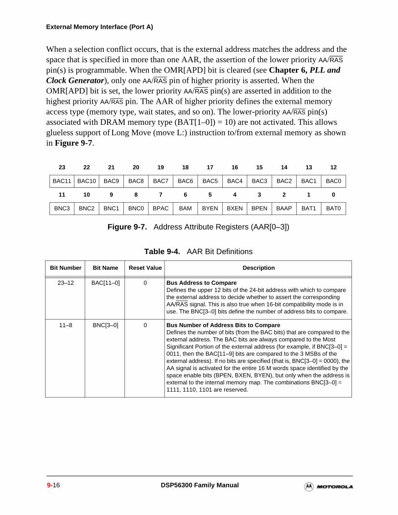
External Memory Interface (Port A)
n
When a selection conflict occurs, that is the external address matches the address and the space that is specified in more than one AAR, the assertion of the lower priority AA/RAS pin(s) is programmable. When the OMR[APD] bit is cleared (see Chapter 6, PLL and Clock Generator), only one AA/RAS pin of higher priority is asserted. When the OMR[APD] bit is set, the lower priority AA/RAS pin(s) are asserted in addition to the highest priority AA/RAS pin. The AAR of higher priority defines the external memory access type (memory type, wait states, and so on). The lower-priority AA/RAS pin(s) associated with DRAM memory type (BAT[1–0]) = 10) are not activated. This allowsglueless support of Long Move (move L:) instruction to/from external memory as showin Figure 9-7.
Figure 9-7. Address Attribute Registers (AAR[0–3])
Table 9-4. AAR Bit Definitions
Bit Number Bit Name Reset Value Description
23–12 BAC[11–0] 0 Bus Address to CompareDefines the upper 12 bits of the 24-bit address with which to compare the external address to decide whether to assert the corresponding AA/RAS signal. This is also true when 16-bit compatibility mode is in use. The BNC[3–0] bits define the number of address bits to compare.
11–8 BNC[3–0] 0 Bus Number of Address Bits to CompareDefines the number of bits (from the BAC bits) that are compared to the external address. The BAC bits are always compared to the Most Significant Portion of the external address (for example, if BNC[3–0] = 0011, then the BAC[11–9] bits are compared to the 3 MSBs of the external address). If no bits are specified (that is, BNC[3–0] = 0000), the AA signal is activated for the entire 16 M words space identified by the space enable bits (BPEN, BXEN, BYEN), but only when the address is external to the internal memory map. The combinations BNC[3–0] = 1111, 1110, 1101 are reserved.
23 22 21 20 19 18 17 16 15 14 13 12
BAC11 BAC10 BAC9 BAC8 BAC7 BAC6 BAC5 BAC4 BAC3 BAC2 BAC1 BAC0
11 10 9 8 7 6 5 4 3 2 1 0
BNC3 BNC2 BNC1 BNC0 BPAC BAM BYEN BXEN BPEN BAAP BAT1 BAT0
9-16 DSP56300 Family Manual
Port A Control
7 BPAC 0 Bus Packing Enable Defines whether the internal packing/unpacking logic is enabled. When the BPAC bit is set, packing is enabled. In this mode each DMA external access initiates three external accesses to 8-bit wide external memory (the addresses for these accesses are DAB, then DAB + 1 and then DAB + 2). Packing to a 24-bit word (or unpacking from a 24-bit word to three 8-bit words) is done automatically by the expansion port control hardware. The external memory should reside in the eight Least Significant Bits (LSBs) of the external data bus, and the packing (or unpacking for external write accesses) is done in “Little Endian” order (that is, the low byte is stored in the lowest of the three memory locations and is transferred first; the middle byte is stored/transferred next; and the high byte is stored/transferred last). When this bit is cleared, the expansion port control logic assumes a 24-bit wide external memory.
NOTE: The BPAC bit is used only for DMA accesses and not core accesses. To ensure sequential external accesses, the DMA address should advance three steps at a time in two-dimensional mode with a row length of one and an offset size of three. Refer to Motorola application note, APR23/D, Using the DSP56300 Direct Memory Access Controller, for more information.
To prevent improper operation, DMA address + 1 and DMA address + 2 should not cross the AAR bank borders.
Arbitration is not allowed during the packing access (that is, the three accesses are treated as one access with respect to arbitration, and bus mastership is not released during these accesses)
6 BAM 0 Bus Address Multiplexing Defines whether the eight LSBs of the address appear on address lines A0–A7 (Least Significant Portion of the external address bus) or on address lines A16–A23 (Most Significant Portion of the external address bus). When BAM is set, the eight LSBs appear on address lines A16–A23. When BAM is cleared, the eight LSBs appear normally on address lines A0–A7. This feature enables you to connect an external peripheral to the MSBs of the address, thus decreasing the load on the Least Significant Portion of the external address and enabling a more efficient interface to external memories. BAM is ignored during DRAM access (BAT[1–0] = 10).
NOTE: The BAM bit has no effect in DSP56300 core devices with only eighteen address lines.
5 BYEN 0 Bus Y Data Memory EnableDefines whether the AA/RAS pin and logic should be activated during external Y data space accesses. When set, BYEN enables the comparison of the external address to the BAC bits during external Y data space accesses. If BYEN is cleared, no address comparison is performed during external Y data space accesses.
Table 9-4. AAR Bit Definitions (Continued)
Bit Number Bit Name Reset Value Description
External Memory Interface (Port A) 9-17
External Memory Interface (Port A)
4 BXEN 0 Bus X Data Memory EnableDefines whether the AA/RAS pin and logic should be activated during external X data space accesses. When set, BXEN enables the comparison of the external address to the BAC bits during external X data space accesses. If BXEN is cleared, no address comparison is performed during external X data space accesses.
3 BPEN 0 Bus Program Memory EnableDefines whether or not the AA/RAS pin and logic should be activated during external program space accesses. When set, BPEN enables the comparison of the external address to the BAC bits during external program space accesses. If BPEN is cleared, no address comparison is performed during external program space accesses.
2 BAAP 0 Bus Address Attribute PolarityDefines whether the AA/RAS signal is active low or active high. When BAAP is cleared, the AA/RAS signal is active low (useful for enabling memory modules or for DRAM Row Address Strobe). If BAAP is set, the appropriate AA/RAS signal is active high (useful as an additional address bit).
1–0 BAT[1–0] 0 Bus Access TypeDefine the type of external memory (DRAM or SRAM) to access for the area defined by the BAC[11–0], BYEN, BXEN, and BPEN bits. The encoding of BAT[1–0] is:00 = Reserved01 = SRAM access10 = DRAM access11 = ReservedWhen the external access type is defined as DRAM access (BAT[1–0] = 10), AA/RAS acts as a Row Address Strobe (RAS) signal. Otherwise, it acts as an Address Attribute signal. External accesses to the default area are always executed as if BAT[1–0] = 01 (that is, SRAM access).
NOTE: If Port A is used for external accesses, the BAT bits in AAR[0–3] must be initialized to the SRAM access type (that is, BAT = 01) or to the DRAM access type (that is, BAT = 10). To ensure proper operation of Port A, this initialization must occur even for an AAR register that is not used during a Port A access. At reset the BAT bits are initialized to 00.
Table 9-4. AAR Bit Definitions (Continued)
Bit Number Bit Name Reset Value Description
9-18 DSP56300 Family Manual
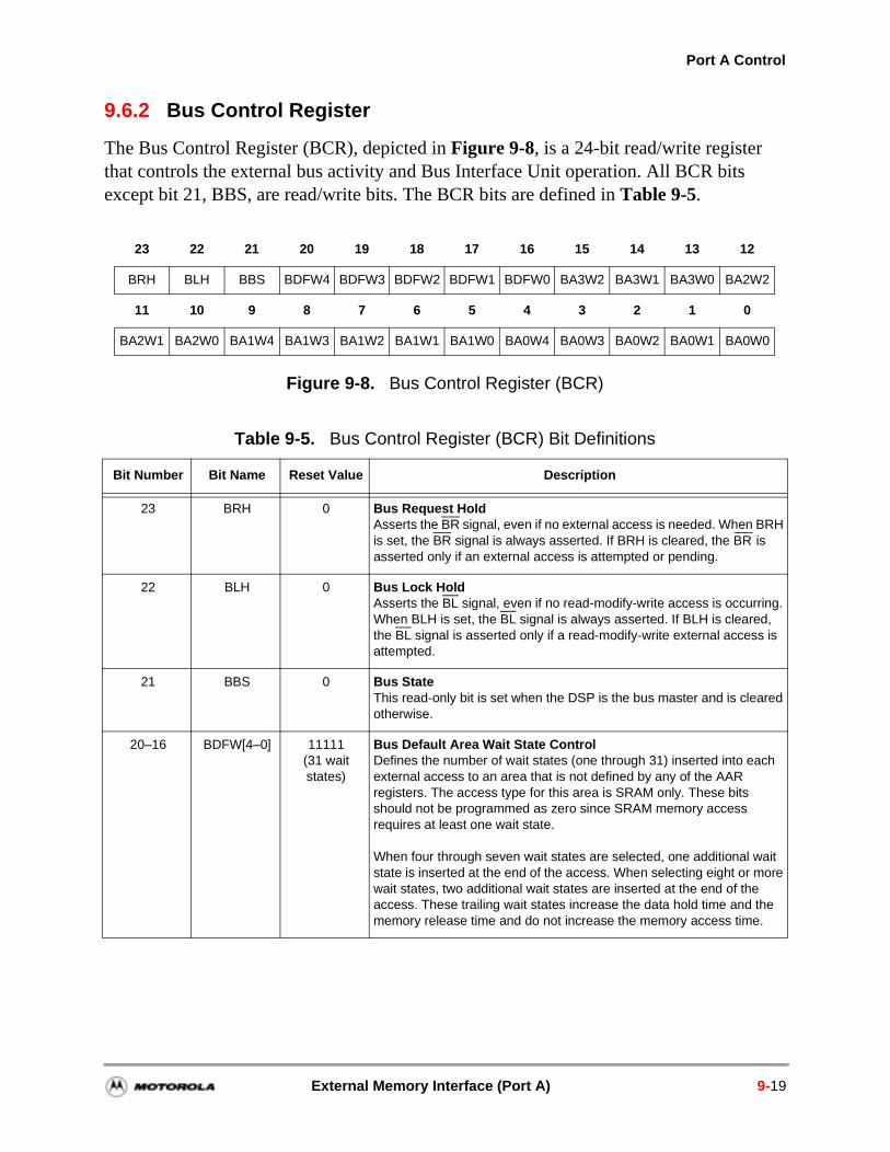
Port A Control
9.6.2 Bus Control Register
The Bus Control Register (BCR), depicted in Figure 9-8, is a 24-bit read/write register that controls the external bus activity and Bus Interface Unit operation. All BCR bits except bit 21, BBS, are read/write bits. The BCR bits are defined in Table 9-5.
Figure 9-8. Bus Control Register (BCR)
Table 9-5. Bus Control Register (BCR) Bit Definitions
Bit Number Bit Name Reset Value Description
23 BRH 0 Bus Request HoldAsserts the BR signal, even if no external access is needed. When BRH is set, the BR signal is always asserted. If BRH is cleared, the BR is asserted only if an external access is attempted or pending.
22 BLH 0 Bus Lock Hold Asserts the BL signal, even if no read-modify-write access is occurring. When BLH is set, the BL signal is always asserted. If BLH is cleared, the BL signal is asserted only if a read-modify-write external access is attempted.
21 BBS 0 Bus StateThis read-only bit is set when the DSP is the bus master and is cleared otherwise.
20–16 BDFW[4–0] 11111(31 wait states)
Bus Default Area Wait State ControlDefines the number of wait states (one through 31) inserted into each external access to an area that is not defined by any of the AAR registers. The access type for this area is SRAM only. These bits should not be programmed as zero since SRAM memory access requires at least one wait state.
When four through seven wait states are selected, one additional wait state is inserted at the end of the access. When selecting eight or more wait states, two additional wait states are inserted at the end of the access. These trailing wait states increase the data hold time and the memory release time and do not increase the memory access time.
23 22 21 20 19 18 17 16 15 14 13 12
BRH BLH BBS BDFW4 BDFW3 BDFW2 BDFW1 BDFW0 BA3W2 BA3W1 BA3W0 BA2W2
11 10 9 8 7 6 5 4 3 2 1 0
BA2W1 BA2W0 BA1W4 BA1W3 BA1W2 BA1W1 BA1W0 BA0W4 BA0W3 BA0W2 BA0W1 BA0W0
External Memory Interface (Port A) 9-19
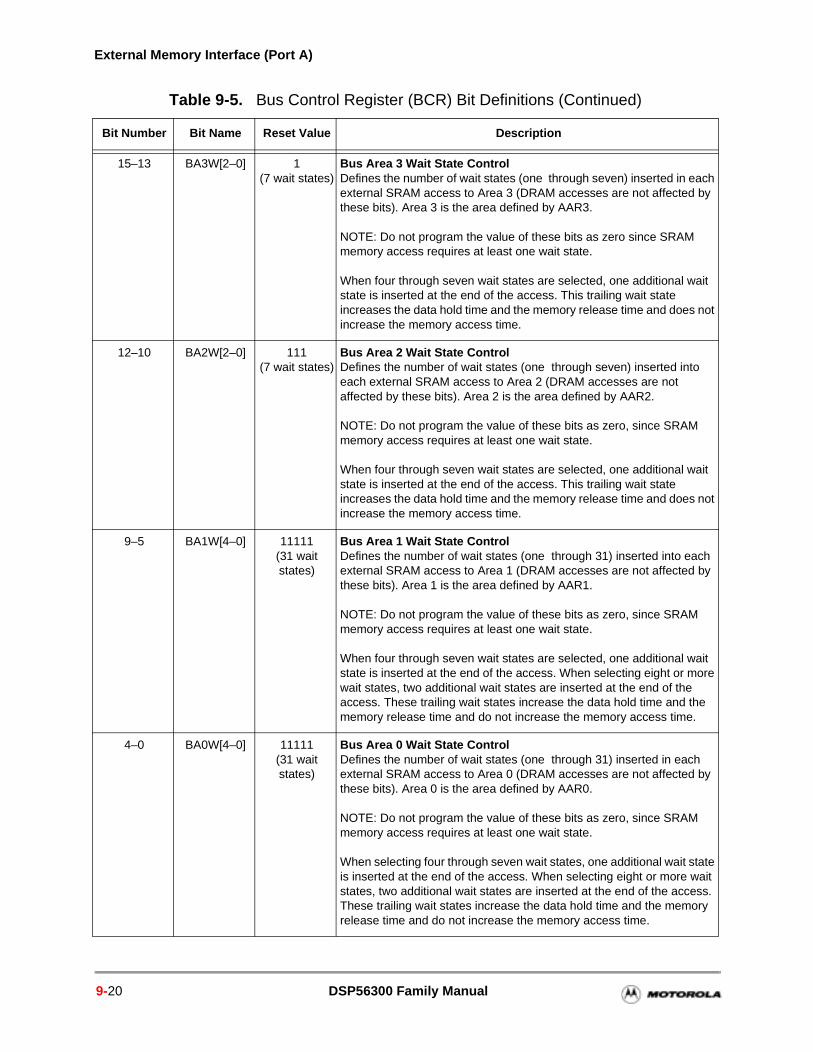
External Memory Interface (Port A)
15–13 BA3W[2–0] 1 (7 wait states)
Bus Area 3 Wait State ControlDefines the number of wait states (one through seven) inserted in each external SRAM access to Area 3 (DRAM accesses are not affected by these bits). Area 3 is the area defined by AAR3.
NOTE: Do not program the value of these bits as zero since SRAM memory access requires at least one wait state.
When four through seven wait states are selected, one additional wait state is inserted at the end of the access. This trailing wait state increases the data hold time and the memory release time and does not increase the memory access time.
12–10 BA2W[2–0] 111 (7 wait states)
Bus Area 2 Wait State ControlDefines the number of wait states (one through seven) inserted into each external SRAM access to Area 2 (DRAM accesses are not affected by these bits). Area 2 is the area defined by AAR2.
NOTE: Do not program the value of these bits as zero, since SRAM memory access requires at least one wait state.
When four through seven wait states are selected, one additional wait state is inserted at the end of the access. This trailing wait state increases the data hold time and the memory release time and does not increase the memory access time.
9–5 BA1W[4–0] 11111 (31 wait states)
Bus Area 1 Wait State ControlDefines the number of wait states (one through 31) inserted into each external SRAM access to Area 1 (DRAM accesses are not affected by these bits). Area 1 is the area defined by AAR1.
NOTE: Do not program the value of these bits as zero, since SRAM memory access requires at least one wait state.
When four through seven wait states are selected, one additional wait state is inserted at the end of the access. When selecting eight or more wait states, two additional wait states are inserted at the end of the access. These trailing wait states increase the data hold time and the memory release time and do not increase the memory access time.
4–0 BA0W[4–0] 11111 (31 wait states)
Bus Area 0 Wait State ControlDefines the number of wait states (one through 31) inserted in each external SRAM access to Area 0 (DRAM accesses are not affected by these bits). Area 0 is the area defined by AAR0.
NOTE: Do not program the value of these bits as zero, since SRAM memory access requires at least one wait state.
When selecting four through seven wait states, one additional wait state is inserted at the end of the access. When selecting eight or more wait states, two additional wait states are inserted at the end of the access. These trailing wait states increase the data hold time and the memory release time and do not increase the memory access time.
Table 9-5. Bus Control Register (BCR) Bit Definitions (Continued)
Bit Number Bit Name Reset Value Description
9-20 DSP56300 Family Manual
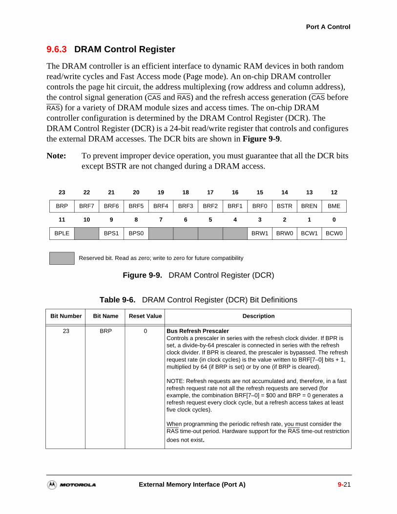
Port A Control
9.6.3 DRAM Control Register
The DRAM controller is an efficient interface to dynamic RAM devices in both random read/write cycles and Fast Access mode (Page mode). An on-chip DRAM controller controls the page hit circuit, the address multiplexing (row address and column address), the control signal generation (CAS and RAS) and the refresh access generation (CAS before RAS) for a variety of DRAM module sizes and access times. The on-chip DRAM controller configuration is determined by the DRAM Control Register (DCR). The DRAM Control Register (DCR) is a 24-bit read/write register that controls and configures the external DRAM accesses. The DCR bits are shown in Figure 9-9.
Note: To prevent improper device operation, you must guarantee that all the DCR bits except BSTR are not changed during a DRAM access.
Figure 9-9. DRAM Control Register (DCR)
Table 9-6. DRAM Control Register (DCR) Bit Definitions
Bit Number Bit Name Reset Value Description
23 BRP 0 Bus Refresh Prescaler Controls a prescaler in series with the refresh clock divider. If BPR is set, a divide-by-64 prescaler is connected in series with the refresh clock divider. If BPR is cleared, the prescaler is bypassed. The refresh request rate (in clock cycles) is the value written to BRF[7–0] bits + 1, multiplied by 64 (if BRP is set) or by one (if BRP is cleared).
NOTE: Refresh requests are not accumulated and, therefore, in a fast refresh request rate not all the refresh requests are served (for example, the combination BRF[7–0] = $00 and BRP = 0 generates a refresh request every clock cycle, but a refresh access takes at least five clock cycles).
When programming the periodic refresh rate, you must consider the RAS time-out period. Hardware support for the RAS time-out restriction
does not exist.
23 22 21 20 19 18 17 16 15 14 13 12
BRP BRF7 BRF6 BRF5 BRF4 BRF3 BRF2 BRF1 BRF0 BSTR BREN BME
11 10 9 8 7 6 5 4 3 2 1 0
BPLE BPS1 BPS0 BRW1 BRW0 BCW1 BCW0
Reserved bit. Read as zero; write to zero for future compatibility
External Memory Interface (Port A) 9-21
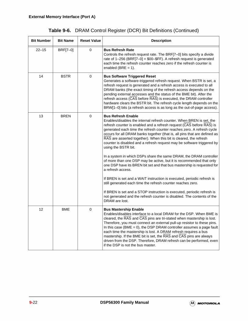
External Memory Interface (Port A)
22–15 BRF[7–0] 0 Bus Refresh RateControls the refresh request rate. The BRF[7–0] bits specify a divide rate of 1–256 (BRF[7–0] = $00–$FF). A refresh request is generated each time the refresh counter reaches zero if the refresh counter is enabled (BRE = 1).
14 BSTR 0 Bus Software Triggered ResetGenerates a software-triggered refresh request. When BSTR is set, a refresh request is generated and a refresh access is executed to all DRAM banks (the exact timing of the refresh access depends on the pending external accesses and the status of the BME bit). After the refresh access (CAS before RAS) is executed, the DRAM controller hardware clears the BSTR bit. The refresh cycle length depends on the BRW[1–0] bits (a refresh access is as long as the out-of-page access).
13 BREN 0 Bus Refresh EnableEnables/disables the internal refresh counter. When BREN is set, the refresh counter is enabled and a refresh request (CAS before RAS) is generated each time the refresh counter reaches zero. A refresh cycle occurs for all DRAM banks together (that is, all pins that are defined as RAS are asserted together). When this bit is cleared, the refresh counter is disabled and a refresh request may be software triggered by using the BSTR bit.
In a system in which DSPs share the same DRAM, the DRAM controller of more than one DSP may be active, but it is recommended that only one DSP have its BREN bit set and that bus mastership is requested for a refresh access.
If BREN is set and a WAIT instruction is executed, periodic refresh is still generated each time the refresh counter reaches zero.
If BREN is set and a STOP instruction is executed, periodic refresh is not generated and the refresh counter is disabled. The contents of the DRAM are lost.
12 BME 0 Bus Mastership EnableEnables/disables interface to a local DRAM for the DSP. When BME is cleared, the RAS and CAS pins are tri-stated when mastership is lost. Therefore, you must connect an external pull-up resistor to these pins. In this case (BME = 0), the DSP DRAM controller assumes a page fault each time the mastership is lost. A DRAM refresh requires a bus mastership. If the BME bit is set, the RAS and CAS pins are always driven from the DSP. Therefore, DRAM refresh can be performed, even if the DSP is not the bus master.
Table 9-6. DRAM Control Register (DCR) Bit Definitions (Continued)
Bit Number Bit Name Reset Value Description
9-22 DSP56300 Family Manual
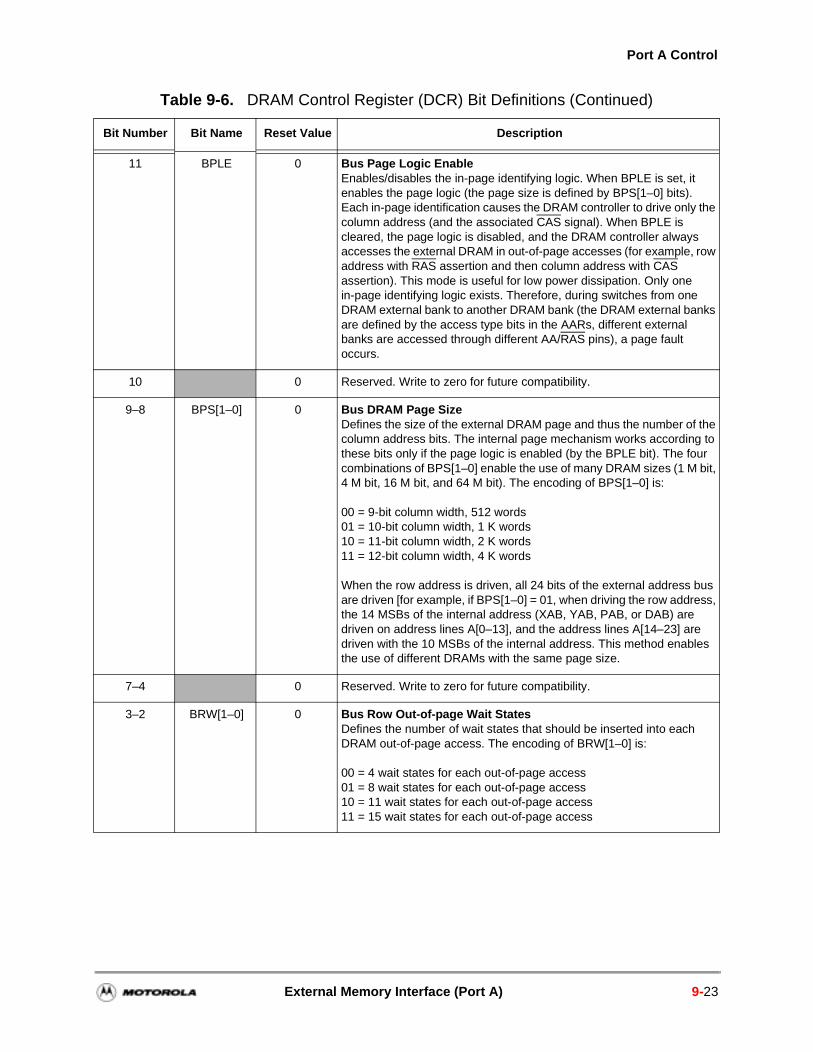
Port A Control
11 BPLE 0 Bus Page Logic EnableEnables/disables the in-page identifying logic. When BPLE is set, it enables the page logic (the page size is defined by BPS[1–0] bits). Each in-page identification causes the DRAM controller to drive only the column address (and the associated CAS signal). When BPLE is cleared, the page logic is disabled, and the DRAM controller always accesses the external DRAM in out-of-page accesses (for example, row address with RAS assertion and then column address with CAS assertion). This mode is useful for low power dissipation. Only one in-page identifying logic exists. Therefore, during switches from one DRAM external bank to another DRAM bank (the DRAM external banks are defined by the access type bits in the AARs, different external banks are accessed through different AA/RAS pins), a page fault occurs.
10 0 Reserved. Write to zero for future compatibility.
9–8 BPS[1–0] 0 Bus DRAM Page SizeDefines the size of the external DRAM page and thus the number of the column address bits. The internal page mechanism works according to these bits only if the page logic is enabled (by the BPLE bit). The four combinations of BPS[1–0] enable the use of many DRAM sizes (1 M bit, 4 M bit, 16 M bit, and 64 M bit). The encoding of BPS[1–0] is:
00 = 9-bit column width, 512 words01 = 10-bit column width, 1 K words10 = 11-bit column width, 2 K words11 = 12-bit column width, 4 K words
When the row address is driven, all 24 bits of the external address bus are driven [for example, if BPS[1–0] = 01, when driving the row address, the 14 MSBs of the internal address (XAB, YAB, PAB, or DAB) are driven on address lines A[0–13], and the address lines A[14–23] are driven with the 10 MSBs of the internal address. This method enables the use of different DRAMs with the same page size.
7–4 0 Reserved. Write to zero for future compatibility.
3–2 BRW[1–0] 0 Bus Row Out-of-page Wait StatesDefines the number of wait states that should be inserted into each DRAM out-of-page access. The encoding of BRW[1–0] is:
00 = 4 wait states for each out-of-page access01 = 8 wait states for each out-of-page access10 = 11 wait states for each out-of-page access11 = 15 wait states for each out-of-page access
Table 9-6. DRAM Control Register (DCR) Bit Definitions (Continued)
Bit Number Bit Name Reset Value Description
External Memory Interface (Port A) 9-23
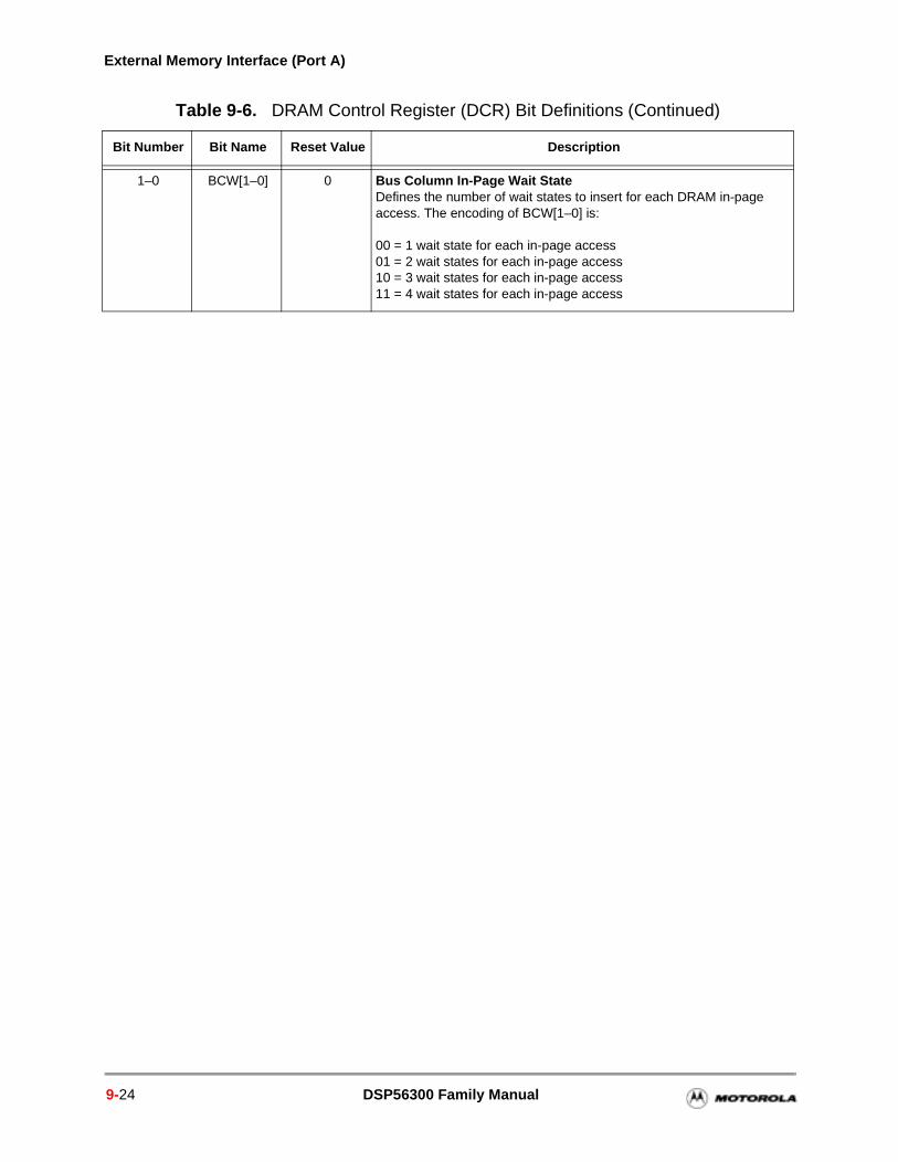
External Memory Interface (Port A)
1–0 BCW[1–0] 0 Bus Column In-Page Wait StateDefines the number of wait states to insert for each DRAM in-page access. The encoding of BCW[1–0] is:
00 = 1 wait state for each in-page access01 = 2 wait states for each in-page access10 = 3 wait states for each in-page access11 = 4 wait states for each in-page access
Table 9-6. DRAM Control Register (DCR) Bit Definitions (Continued)
Bit Number Bit Name Reset Value Description
9-24 DSP56300 Family Manual
ove-
Chapter 10DMA Controller
Direct Memory Access (DMA) is one of several methods for coordinating the timing of data transfers between an input/output (I/O) device and the core processing unit or memory in a computer. DMA is one of the faster types of synchronization mechanisms, generally providing significant improvement over interrupts, in terms of both latency and throughput. An I/O device often operates at a much slower speed than the core.1 DMA allows the I/O device to access the memory directly, without using the core. DMA can lead to a significant improvement in performance because data movement is one of the most common operations performed in processing applications. There are several advantages of using DMA, rather than the core, in the DSP56300 family:
DMA saves core MIPS because the core can operate in parallel.
DMA saves power because it requires less circuitry than the core to move data.
DMA saves pointers because core AGU pointer registers are not needed.
DMA has no modulo block size restrictions, unlike the core AGU.
Traditionally, DMA uses the same internal address and data buses as the core. Consequently, when DMA performs one or more word transfers, it can cause the core to temporarily halt activity for one or more cycles while DMA moves the data. With this type of architecture, the core and DMA cannot both perform data moves in the same core clock cycle. To overcome data movement restrictions imposed by sharing resources with the core, the DMA system in the DSP56300 family contains its own dedicated internal address and data buses. Internal memory is partitioned so that the Program Control Unit (PCU) and DMA can both perform internal memory accesses in the same core clock cycle, as long they are accessing different memory partitions. Also, if one of these two controllers (PCU or DMA) is accessing internal memory, the other controller can perform an external memory access in the same core clock cycle.
1. The term “core” has a special meaning when described in the context of DMA. Technically, the DSP56300 core contains all of the circuitry that is common to all devices in the DSP56300 family, including the DMA controller and buses. However, when described in the context of DMA, the core actions referred to are those caused by data movement instructions executed by the PCU, not data mment performed by DMA.
DSP56300 Family Manual 10-1
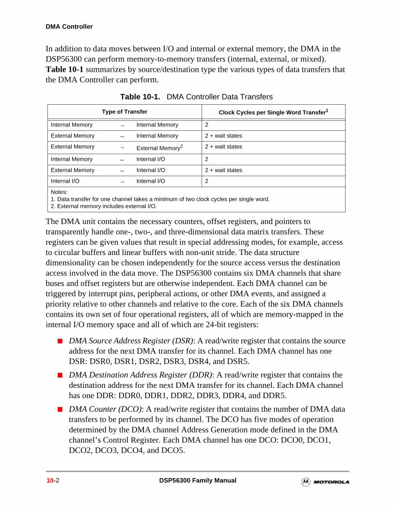
DMA Controller
In addition to data moves between I/O and internal or external memory, the DMA in the DSP56300 can perform memory-to-memory transfers (internal, external, or mixed). Table 10-1 summarizes by source/destination type the various types of data transfers that the DMA Controller can perform.
The DMA unit contains the necessary counters, offset registers, and pointers to transparently handle one-, two-, and three-dimensional data matrix transfers. These registers can be given values that result in special addressing modes, for example, access to circular buffers and linear buffers with non-unit stride. The data structure dimensionality can be chosen independently for the source access versus the destination access involved in the data move. The DSP56300 contains six DMA channels that share buses and offset registers but are otherwise independent. Each DMA channel can be triggered by interrupt pins, peripheral actions, or other DMA events, and assigned a priority relative to other channels and relative to the core. Each of the six DMA channels contains its own set of four operational registers, all of which are memory-mapped in the internal I/O memory space and all of which are 24-bit registers:
DMA Source Address Register (DSR): A read/write register that contains the source address for the next DMA transfer for its channel. Each DMA channel has one DSR: DSR0, DSR1, DSR2, DSR3, DSR4, and DSR5.
DMA Destination Address Register (DDR): A read/write register that contains the destination address for the next DMA transfer for its channel. Each DMA channel has one DDR: DDR0, DDR1, DDR2, DDR3, DDR4, and DDR5.
DMA Counter (DCO): A read/write register that contains the number of DMA data transfers to be performed by its channel. The DCO has five modes of operation determined by the DMA channel Address Generation mode defined in the DMA channel’s Control Register. Each DMA channel has one DCO: DCO0, DCO1,DCO2, DCO3, DCO4, and DCO5.
Table 10-1. DMA Controller Data Transfers
Type of Transfer Clock Cycles per Single Word Transfer1
Internal Memory → Internal Memory 2
External Memory ↔ Internal Memory 2 + wait states
External Memory → External Memory2 2 + wait states
Internal Memory ↔ Internal I/O 2
External Memory ↔ Internal I/O 2 + wait states
Internal I/O → Internal I/O 2
Notes:1. Data transfer for one channel takes a minimum of two clock cycles per single word.2. External memory includes external I/O.
10-2 DSP56300 Family Manual
DMA Operational Overview
of
mn
e for
DMA Control Register (DCR): A read/write register that controls the operation of a DMA channel. Each DMA channel has one DCR: DCR0, DCR1, DCR2, DCR3, DCR4 and DCR5.
The DMA Controller also has supporting 24-bit registers available to all the DMA channels:
DMA Offset Register (DOR): Each DOR is a read/write register that contains the offset value to be used in some of the DMA addressing modes. The DMA controller has four common offset registers (DOR0, DOR1, DOR2, and DOR3) that can be used by all the channels according to their Address Generation mode.
DMA Status Register (DSTR): This read-only register reflects the overall operating status of all channels in the DMA Controller.
In summary, the DSP56300 DMA can perform I/O and memory accesses that are independent of and frequently simultaneous with PCU operations. DMA can transfer memory-to-memory and handle mixed multi-dimensional and special address mode transfers. DMA contains six highly independent channels with separate priorities and multiple trigger choices. These capabilities significantly enhance code performance.
10.1 DMA Operational Overview
The following subsections describe how the DSP56300 DMA operates. These subsections are organized by function, rather than by event sequence. The DMA register description section contains detailed operational information.
10.1.1 Basic Address Modes
The DSP56300 DMA can deal with the following basic types of data structures:
Constant Addressing: This mode uses a single address throughout the data transfer. Typically this is used by I/O devices that use a single address to transfer information.
One-dimensional: A one-dimensional matrix consisting of one item or a “line” items located in consecutive memory locations.
Two-dimensional: A two-dimensional matrix or table that is stored in row-coluorder with equal spacing in memory between each row or line.
Three-dimensional: A three-dimensional matrix or collection of tables that areequally spaced in memory.
The type of data structure is specified in the counter mode for the DMA channel. Thcounter mode divides a given 24-bit counter register into one or more sections, one
DMA Controller 10-3
DMA Controller
in a d on the
of s
s
rd ree.
o een
; the nsion ode
e
its ated pper
each dimension used. The appropriate counter fields either decrement or reload each time the DMA transfers a data word. A counter field is reloaded with its initial value after that field is decremented to zero. For details on counter operation, see Section 10.5.3, DMA Counters (DCO[5–0]), on page 10-10. Once all fields in the counter are exhausted, one or more data moves are performed and all words, lines, and tables are transferred. The total collection of data moved is called the “block.” Exhaustion of the entire counter resultssingle “block transfer.” The automatic counter register updates are directly performethe user-visible counter register. In other words, the counter register is used for bothcount load/reload function and the count decrement function.
10.1.2 Special Address Modes
The counter and offset registers can be loaded with special values to produce variants the basic addressing modes. Some examples covered in more detail in later sectioninclude:
Circular buffer: Use a two-dimensional counter and a negative offset that wrapback to the buffer start address.
Linear buffer with non-unit stride: Use a two-dimensional counter with one woper row. This method must be used with byte packing, which has a stride of th
A larger-than-normal field width in a two-dimensional counter: Concatenate twfields in a three-dimensional counter by specifying an offset value of one betwthem.
10.1.3 Unmatched Source and Destination Dimensions
The source and destination data structures can have different dimensions.2 The data structure with the largest dimension is read or written once during the block transferdata structure with the smaller dimension can be written or read repeatedly. For thissituation, a single counter register handles both sides of the transfer. The high-dime(three-dimensional or two-dimensional) side of the transfer determines the counter mand thus the number of available counter fields. Each “tick” of the counter counts onword transfer; that is, one source read and one destination write.
The data structure on the low-dimension side of the transfer is fully described by a right-justified subset of the counter—the number of counter fields being the same asdimension (two-dimensional or one-dimensional). This data structure access is repe(using the exact same addressing sequence) the number of times specified by the u
2. For an example, see the Motorola application report, APR/23, Using the DSP56300 Direct Memory Access Controller.
10-4 DSP56300 Family Manual
DMA Operational Overview
l)
r an not
rding
urce, ple, nnel that is de. or re
field(s) of the counter. The pointer wraparound back to the beginning of this data structure is accomplished using a negative offset register value, similar to a circular buffer.
10.1.4 DMA Triggers (Request Sources)
Data movement in by a particular DMA channel is initiated by either a hardware or a software trigger. Following is an example list of some of the hardware and software DMA triggers, also known as DMA request sources. Peripheral triggers are device-dependent. A DMA channel can be configured for triggering by only one source at a time.
Hardware triggers
— External interrupt pins (IRQ[A–D])
— DMA channel block transfer completion (by this or a different DMA channe
— Peripheral status bits
— Receiver has new datum to be read by DMA
— Transmitter needs new datum from DMA to send
— Timer compare event
Software triggers
— DMA Enable bit for this DMA channel
A peripheral status bit that triggers an enabled DMA transfer also typically can triggeenabled peripheral interrupt. The DMA transfer is triggered by the status bit change,by the peripheral interrupt event, and the DMA transfer occurs whether or not the peripheral interrupt is enabled. Furthermore, avoid triggering a DMA transfer and a peripheral interrupt from the same event; this can result in a lack of coordination regaresources and status bit changes.
10.1.5 Transfer Mode
When a DMA channel is enabled and receives a trigger from its configured trigger soit begins moving data as soon as the needed resources become available (for examinternal DMA buses and memory locations). As a result of the trigger event, the chatransfers either all or a subset of the block (this is configurable). The amount of data transferred in response to each trigger event is determined by the DMA transfer moBesides the trigger data structure, the transfer mode also selects either a hardware software trigger, and automatic block repeat enable. The available transfer modes asingle word, line, and block. Typically, a DMA channel used in conjunction with a peripheral operates in a single word transfer mode (triggered by a receiver full or transmitter empty condition).
DMA Controller 10-5
DMA Controller
often ate
iven e read r all
el
d one
nel A ock ed by
10.2 Timing (Core Clock Cycles)
This section describes the timing of core and DMA data transfers in the context of integral core clock cycle counts. When the needed resources are available, each word transfer performed by the DMA takes at least two core clock cycles:
Source read (at least one cycle)
Destination write (at least one cycle)
Any wait states incurred during external memory accesses are added to the DMA word transfer time (for external source and/or destination).
Some peripherals (generally those using first-in-first-out (FIFO) for data transfer) may act as “fast DMA request sources.” These peripherals can trigger a new DMA request asas every two core clock cycles, thereby using the DMA at its maximum throughput rwith zero overhead time.
10.2.1 Non-Overlap Between DMA Channels
Data movement can never be performed by more than one DMA channel within a gcore clock cycle. For example, it is not possible for Channel 1 to commence its sourcbefore Channel 0 completes its destination write. This non-overlap limitation exists fosituations, including the following cases:
One channel needs to read (write) from external memory, and another channneeds to write (read) to internal memory.
One of the DMA channels is waiting on the Bus Interface Unit (BIU) for an external access to complete, and the BIU is in turn waiting because of:
— Static wait states (determined by Bus Control Register)
— Dynamic wait states (controlled by TA pin)
— Byte packing
This limitation is necessary because there is only one internal DMA address bus aninternal DMA data bus. The internal DMA buses are in use by a DMA channel even during the external memory access phase of the DMA word transfer. Although chanoverlap during DMA channel transfers cannot exist, zero overhead between two DMchannel transfers can exist. Once the word transfer performed by a DMA channel iscompleted, another DMA channel can begin data movement in the very next core clcycle—if the second DMA channel has already been triggered and is not being delaycontention or priority issues.
10-6 DSP56300 Family Manual
Channel Priority
has
rnal
ng a d ntrol for in this
ls.
of
een
10.2.2 Overlap between DMA Channel and Core
Since the core and DMA use separate address and data buses, both can perform data movement in a given core clock cycle. This overlap of data movement can occur for the following cases:
The core is accessing internal memory while DMA is accessing a different internal memory partition:
— RAM: 1/4 K words partition size (this size is device-dependent)
— ROM: 2, 3, or 4 K words device-specific partition size
If the core and DMA try to access the same internal memory partition, the corepriority and DMA is delayed.
The core is accessing internal (external) memory while DMA is accessing exte(internal) memory
10.3 Channel Priority
DMA channel priority determines if and when a DMA channel can be interrupted duriblock transfer. An interruption occurs between word transfers. The current DMA wortransfer is allowed to complete before the core or another DMA channel can take coof the resource that is under contention. The DMA channel priority arbitration occurseach DMA word transfer; only enabled and already triggered channels can take part arbitration.
10.3.1 Priority Between DMA Channels
Each DMA channel can be independently assigned one of four possible priority leveThe treatment of priorities is as follows:
Channels with different priorities:
A higher-priority DMA channel can interrupt a lower-priority DMA channel andcomplete its block transfer before control transfers back to the lower-priority channel.
Channels with the same priority, one of two different modes can be selected:
— Continuous mode: A DMA channel cannot interrupt another DMA channel the same priority.
— Non-continuous mode: Control is transferred in a round-robin fashion betweach channel of the same priority. Each channel transfers one word beforecontrol transfers to the next channel in this group.
DMA Controller 10-7
DMA Controller
ater
g
the
ere is
a of the e the e entire to nation d with else.
DMA channels cannot interrupt each other in the middle of word transfers, regardless of their relative priorities. A word transfer made by one DMA channel must finish before another DMA channel can commence a word transfer.
10.3.2 Priority Between a DMA Channel and the Core
If the core and a DMA channel are both contending for the same partition of internal memory, but neither has begun the word transfer, the core always takes precedence. The DMA channel must wait until the core is not accessing this memory partition for at least one core clock cycle before it can begin to access the partition.
If the DMA channel and the core are each attempting to access a different internal memory partition in RAM or ROM, no contention exists. In this case, the accesses can be made simultaneously (data movement can occur in both of these data paths in a given core clock cycle). If the core and a DMA channel are both contending to make an external memory access, the prioritizing between that channel and the core is performed according to one of two selectable modes:
Static DMA/Core Prioritizing mode—The core priority is configured to have a constant fixed relationship with the DMA priority, regardless of which DMA channel is considered. The core priority is set to be either lower, equal, or grethan that of the DMA. The individual DMA channels have equal priority when compared to the core, although they may still have unequal priorities when compared to each other. This mode is set using bits CDP[1–0] of the OperatinMode Register.
Dynamic DMA/Core Prioritizing mode—The priority of each DMA channel is individually compared with that of the core. The DMA channel priority setting used for comparison with other DMA channels is also used for comparison withcore. This mode is set using bits CP[1–0] of the Status Register.
Note: Even though DMA and the core have separate address and data buses, thonly one external address and data bus.
The core cannot interrupt a DMA channel in the middle of a word transfer to or fromcontended resource (an internal memory partition, or external memory), regardless core/DMA relative priority. If the DMA channel is already performing an access to thresource, the core must wait until the current DMA word transfer finishes accessing resource before the core can access that resource. The core may have to wait for thDMA word transfer to complete, or it may have to wait only for the DMA source readcomplete. This depends on the destination address of the DMA channel. If the destiof the DMA word transfer is not in the contended resource, then the core can proceeits access to the resource while the DMA performs its destination write somewhere
10-8 DSP56300 Family Manual
Special Uses of DMA With the Bus Interface Unit
10.4 Special Uses of DMA With the Bus Interface Unit
The following subsections describe Bus Interface Unit (BIU) operations that can only be performed using DMA.
10.4.1 Byte Packing
Byte packing is used when the 24-bit data width DSP core interfaces with an 8-bit wide external memory device. Byte packing can be performed only in conjunction with a DMA data move.3 When the DMA channel attempts to read a word from the external memory, it expects a 24-bit value. In accordance with the DMA read, the BIU reads three consecutive bytes from the memory, packs them into one 24-bit word, and then passes this word to the DMA. A reverse sequence occurs for a DMA write to the external memory. The BIU takes the 24-bit word from the DMA channel, unpacks it, and writes it as three consecutive bytes, to the external memory. For both read and write, the DMA views each 24-bit word transfer as a single external access. However, the byte packing operation is not completely transparent to the DMA. To read or write several 24-bit words to or from consecutive locations in the 8-bit memory, the DMA must be programmed to either increase or decrease its external memory address pointer by three for each 24-bit transfer.
10.4.1.1 DRAM In-Page Accesses using DMA
When a DMA channel handles several consecutive in-page DRAM word accesses, a special situation can occur if an in-page access is interrupted by an external memory access initiated either by the core or a different DMA channel. The interrupting operation could be a higher-priority access to external SRAM. After the interrupting operation uses the BIU, the original DMA channel can resume reading or writing the DRAM without losing in-page access. This can occur as long as all in-page access conditions (described in Chapter 9, External Memory Interface (Port A)) remain satisfied.
10.4.1.2 End-of-Block-Transfer Interrupt
Upon completion of a block transfer by a DMA channel, an optional end-of-block-transfer DMA interrupt can be generated. The interrupt service routine (ISR) called by such an interrupt can perform any functions needed at this time. For example, the ISR could reconfigure the DMA channel for the next data block transfer or restart the DMA channel (if it is used in a transfer mode for which no automatic restart is available). Do not confuse an end-of-block-transfer DMA interrupt, also known as a “DMA interrupt,” with a peripheral interrupt. A peripheral interrupt can be generated by the same event that
3. For details, see the Port A Address Attribute Register description in Chapter 9, External Memory Inter-face (Port A), and the Motorola application report, APR23/D, Using the DSP56300 Direct Memory Access Controller.
DMA Controller 10-9
DMA Controller
triggers the DMA channel to move part or all of the block. The DMA End-of-Block-Transfer interrupt cannot be used if DMA is operating in the mode in which DE is not cleared at the end of the block transfer (DTM = 100 or 101).
10.5 DMA Controller Programming Model
Figure 10-1 shows the DMA Controller programming model. The following paragraphs describe the registers and how they are used. Since the six channels share identical sets of registers, each of the four registers in each set is described once.
10.5.1 DMA Source Address Registers (DSR[0–5])
The DSR stores the initial source address specified by and loaded from the DMA requesting device. During the DMA transfer, the DSR contents increment as defined by the D3D and DAM bit settings (except in No Update mode). In two-dimensional mode, the specified DOR updates the DSR after the first set of data transfers completes. In three-dimensional mode, the specified DORs update the DSR twice during the transfer.
10.5.2 DMA Destination Address Registers (DDR[5–0])
The DDR stores the initial destination address specified by and loaded from the DMA requesting device. During the DMA transfer, the DDR contents increment as defined by the D3D and DAM bit settings (except in No Update mode). In two-dimensional mode, the specified DOR updates the DDR after the first set of data transfers completes. In three-dimensional mode, the specified DORs update the DDR twice during the transfer.
10.5.3 DMA Counters (DCO[5–0])
During DMA operation, a Source Address Register (DSR) is associated with one of the counter modes, and the Destination Address Register (DDR) can be associated with another counter mode. The following examples use DSR as an example of the address register used, but the same example is valid for the DDR.
10-10 DSP56300 Family Manual
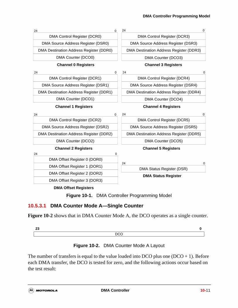
DMA Controller Programming Model
Figure 10-1. DMA Controller Programming Model
10.5.3.1 DMA Counter Mode A—Single Counter
Figure 10-2 shows that in DMA Counter Mode A, the DCO operates as a single counter.
The number of transfers is equal to the value loaded into DCO plus one (DCO + 1). Before each DMA transfer, the DCO is tested for zero, and the following actions occur based on the test result:
Figure 10-2. DMA Counter Mode A Layout
DMA Control Register (DCR5)
DMA Source Address Register (DSR5)
DMA Destination Address Register (DDR5)
DMA Counter (DCO5)
DMA Control Register (DCR4)
DMA Source Address Register (DSR4)
DMA Destination Address Register (DDR4)
DMA Counter (DCO4)
DMA Control Register (DCR3)
DMA Source Address Register (DSR3)
DMA Destination Address Register (DDR3)
DMA Counter (DCO3)
DMA Control Register (DCR2)
DMA Source Address Register (DSR2)
DMA Destination Address Register (DDR2)
DMA Counter (DCO2)
DMA Control Register (DCR1)
DMA Source Address Register (DSR1)
DMA Destination Address Register (DDR1)
DMA Counter (DCO1)
DMA Control Register (DCR0)
DMA Source Address Register (DSR0)
DMA Destination Address Register (DDR0)
DMA Counter (DCO0)
Channel 0 Registers
Channel 1 Registers
Channel 2 Registers
Channel 3 Registers
Channel 4 Registers
Channel 5 Registers
DMA Offset Register 0 (DOR0)
DMA Offset Register 1 (DOR1)
DMA Offset Register 2 (DOR2)
DMA Offset Register 3 (DOR3)
DMA Offset Registers
DMA Status Register (DSR)
DMA Status Register
024
024
024
024
024 024
024
024
23 0
DCO
DMA Controller 10-11
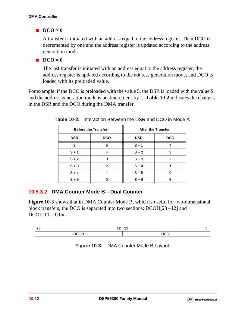
DMA Controller
DCO > 0
A transfer is initiated with an address equal to the address register. Then DCO is decremented by one and the address register is updated according to the address generation mode.
DCO = 0
The last transfer is initiated with an address equal to the address register, the address register is updated according to the address generation mode, and DCO is loaded with its preloaded value.
For example, if the DCO is preloaded with the value 5, the DSR is loaded with the value S, and the address generation mode is postincrement-by-1. Table 10-2 indicates the changes in the DSR and the DCO during the DMA transfer.
10.5.3.2 DMA Counter Mode B—Dual Counter
Figure 10-3 shows that in DMA Counter Mode B, which is useful for two-dimensional block transfers, the DCO is separated into two sections: DCOH[23 –12] and DCOL[11– 0] bits.
Table 10-2. Interaction Between the DSR and DCO in Mode A
Before the Transfer After the Transfer
DSR DCO DSR DCO
S 5 S + 1 4
S + 1 4 S + 2 3
S + 2 3 S + 3 2
S + 3 2 S + 4 1
S + 4 1 S + 5 0
S + 5 0 S + 6 5
Figure 10-3. DMA Counter Mode B Layout
23 12 11 0
DCOH DCOL
10-12 DSP56300 Family Manual
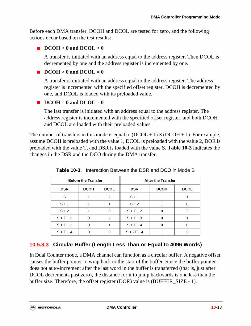
DMA Controller Programming Model
Before each DMA transfer, DCOH and DCOL are tested for zero, and the following actions occur based on the test results:
DCOH > 0 and DCOL > 0
A transfer is initiated with an address equal to the address register. Then DCOL is decremented by one and the address register is incremented by one.
DCOH > 0 and DCOL = 0
A transfer is initiated with an address equal to the address register. The address register is incremented with the specified offset register, DCOH is decremented by one, and DCOL is loaded with its preloaded value.
DCOH = 0 and DCOL = 0
The last transfer is initiated with an address equal to the address register. The address register is incremented with the specified offset register, and both DCOH and DCOL are loaded with their preloaded values.
The number of transfers in this mode is equal to (DCOL + 1) × (DCOH + 1). For example, assume DCOH is preloaded with the value 1, DCOL is preloaded with the value 2, DOR is preloaded with the value T, and DSR is loaded with the value S. Table 10-3 indicates the changes in the DSR and the DCO during the DMA transfer.
10.5.3.3 Circular Buffer (Length Less Than or Equal to 4096 Words)
In Dual Counter mode, a DMA channel can function as a circular buffer. A negative offset causes the buffer pointer to wrap back to the start of the buffer. Since the buffer pointer does not auto-increment after the last word in the buffer is transferred (that is, just after DCOL decrements past zero), the distance for it to jump backwards is one less than the buffer size. Therefore, the offset register (DOR) value is (BUFFER_SIZE - 1).
Table 10-3. Interaction Between the DSR and DCO in Mode B
Before the Transfer After the Transfer
DSR DCOH DCOL DSR DCOH DCOL
S 1 2 S + 1 1 1
S + 1 1 1 S + 2 1 0
S + 2 1 0 S + T + 2 0 2
S + T + 2 0 2 S + T + 3 0 1
S + T + 3 0 1 S + T + 4 0 0
S + T + 4 0 0 S + 2T + 4 1 2
DMA Controller 10-13
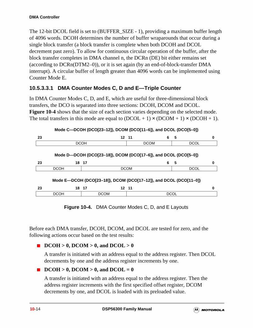
DMA Controller
sing
The 12-bit DCOL field is set to (BUFFER_SIZE - 1), providing a maximum buffer length of 4096 words. DCOH determines the number of buffer wraparounds that occur during a single block transfer (a block transfer is complete when both DCOH and DCOL decrement past zero). To allow for continuous circular operation of the buffer, after the block transfer completes in DMA channel n, the DCRn (DE) bit either remains set (according to DCRn(DTM2–0)), or it is set again (by an end-of-block-transfer DMA interrupt). A circular buffer of length greater than 4096 words can be implemented uCounter Mode E.
10.5.3.3.1 DMA Counter Modes C, D and E—Triple Counter
In DMA Counter Modes C, D, and E, which are useful for three-dimensional block transfers, the DCO is separated into three sections: DCOH, DCOM and DCOL. Figure 10-4 shows that the size of each section varies depending on the selected mode. The total transfers in this mode are equal to (DCOL + 1) × (DCOM + 1) × (DCOH + 1).
Figure 10-4. DMA Counter Modes C, D, and E Layouts
Before each DMA transfer, DCOH, DCOM, and DCOL are tested for zero, and the following actions occur based on the test results:
DCOH > 0, DCOM > 0, and DCOL > 0
A transfer is initiated with an address equal to the address register. Then DCOL decrements by one and the address register increments by one.
DCOH > 0, DCOM > 0, and DCOL = 0
A transfer is initiated with an address equal to the address register. Then the address register increments with the first specified offset register, DCOM decrements by one, and DCOL is loaded with its preloaded value.
Mode C—DCOH (DCO[23–12]), DCOM (DCO[11–6]), and DCOL (DCO[5–0])
Mode D—DCOH (DCO[23–18]), DCOM (DCO[17–6]), and DCOL (DCO[5–0]).
Mode E—DCOH (DCO[23–18]), DCOM (DCO[17–12]), and DCOL (DCO[11–0])
23 12 11 6 5 0
DCOH DCOM DCOL
23 18 17 6 5 0
DCOH DCOM DCOL
23 18 17 12 11 0
DCOH DCOM DCOL
10-14 DSP56300 Family Manual
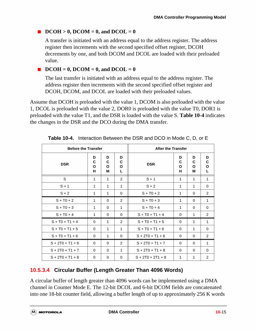
DMA Controller Programming Model
DCOH > 0, DCOM = 0, and DCOL = 0
A transfer is initiated with an address equal to the address register. The address register then increments with the second specified offset register, DCOH decrements by one, and both DCOM and DCOL are loaded with their preloaded value.
DCOH = 0, DCOM = 0, and DCOL = 0
The last transfer is initiated with an address equal to the address register. The address register then increments with the second specified offset register and DCOH, DCOM, and DCOL are loaded with their preloaded values.
Assume that DCOH is preloaded with the value 1, DCOM is also preloaded with the value 1, DCOL is preloaded with the value 2, DOR0 is preloaded with the value T0, DOR1 is preloaded with the value T1, and the DSR is loaded with the value S. Table 10-4 indicates the changes in the DSR and the DCO during the DMA transfer.
10.5.3.4 Circular Buffer (Length Greater Than 4096 Words)
A circular buffer of length greater than 4096 words can be implemented using a DMA channel in Counter Mode E. The 12-bit DCOL and 6-bit DCOM fields are concatenated into one 18-bit counter field, allowing a buffer length of up to approximately 256 K words
Table 10-4. Interaction Between the DSR and DCO in Mode C, D, or E
Before the Transfer After the Transfer
DSR
DCOH
DCOM
DCOL
DSR
DCOH
DCOM
DCOL
S 1 1 2 S + 1 1 1 1
S + 1 1 1 1 S + 2 1 1 0
S + 2 1 1 0 S + T0 + 2 1 0 2
S + T0 + 2 1 0 2 S + T0 + 3 1 0 1
S + T0 + 3 1 0 1 S + T0 + 4 1 0 0
S + T0 + 4 1 0 0 S + T0 + T1 + 4 0 1 2
S + T0 + T1 + 4 0 1 2 S + T0 + T1 + 5 0 1 1
S + T0 + T1 + 5 0 1 1 S + T0 + T1 + 6 0 1 0
S + T0 + T1 + 6 0 1 0 S + 2T0 + T1 + 6 0 0 2
S + 2T0 + T1 + 6 0 0 2 S + 2T0 + T1 + 7 0 0 1
S + 2T0 + T1 + 7 0 0 1 S + 2T0 + T1 + 8 0 0 0
S + 2T0 + T1 + 8 0 0 0 S + 2T0 + 2T1 + 8 1 1 2
DMA Controller 10-15
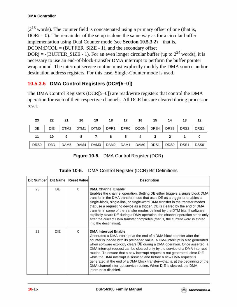
DMA Controller
r d/or
essor
(218 words). The counter field is concatenated using a primary offset of one (that is, DORi = 0). The remainder of the setup is done the same way as for a circular buffer implementation using Dual Counter mode (see Section 10.5.3.2)—that is, DCOM:DCOL = (BUFFER_SIZE - 1), and the secondary offset DORj = -(BUFFER_SIZE - 1). For an even longer circular buffer (up to 224 words), it is necessary to use an end-of-block-transfer DMA interrupt to perform the buffer pointewraparound. The interrupt service routine must explicitly modify the DMA source andestination address registers. For this case, Single-Counter mode is used.
10.5.3.5 DMA Control Registers (DCR[5–0])
The DMA Control Registers (DCR[5–0]) are read/write registers that control the DMA operation for each of their respective channels. All DCR bits are cleared during procreset.
Figure 10-5. DMA Control Register (DCR)
Table 10-5. DMA Control Register (DCR) Bit Definitions
Bit Number Bit Name Reset Value Description
23 DE 0 DMA Channel EnableEnables the channel operation. Setting DE either triggers a single block DMA transfer in the DMA transfer mode that uses DE as a trigger or enables a single-block, single-line, or single-word DMA transfer in the transfer modes that use a requesting device as a trigger. DE is cleared by the end of DMA transfer in some of the transfer modes defined by the DTM bits. If software explicitly clears DE during a DMA operation, the channel operation stops only after the current DMA transfer completes (that is, the current word is stored into the destination).
22 DIE 0 DMA Interrupt EnableGenerates a DMA interrupt at the end of a DMA block transfer after the counter is loaded with its preloaded value. A DMA interrupt is also generated when software explicitly clears DE during a DMA operation. Once asserted, a DMA interrupt request can be cleared only by the service of a DMA interrupt routine. To ensure that a new interrupt request is not generated, clear DIE while the DMA interrupt is serviced and before a new DMA request is generated at the end of a DMA block transfer—that is, at the beginning of the DMA channel interrupt service routine. When DIE is cleared, the DMA interrupt is disabled.
23 22 21 20 19 18 17 16 15 14 13 12
DE DIE DTM2 DTM1 DTM0 DPR1 DPR0 DCON DRS4 DRS3 DRS2 DRS1
11 10 9 8 7 6 5 4 3 2 1 0
DRS0 D3D DAM5 DAM4 DAM3 DAM2 DAM1 DAM0 DDS1 DDS0 DSS1 DSS0
10-16 DSP56300 Family Manual
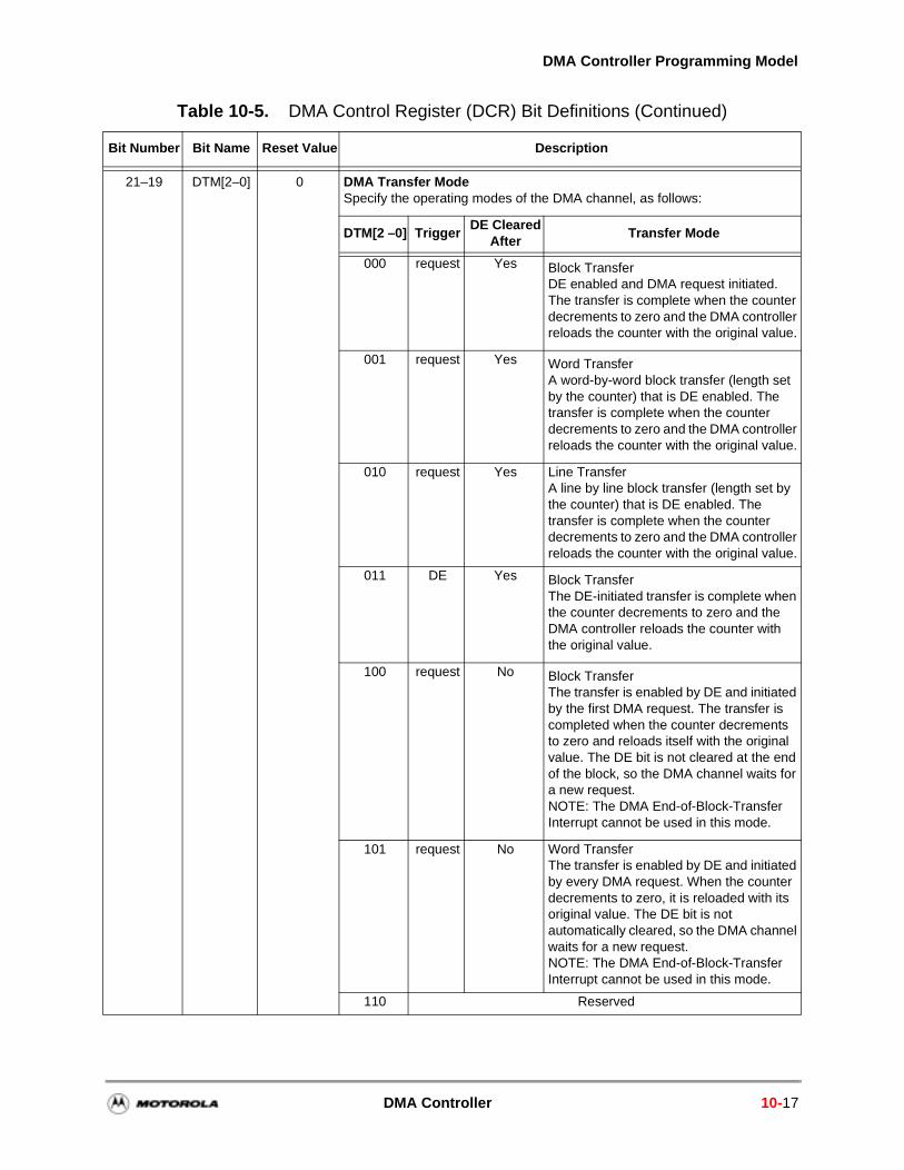
DMA Controller Programming Model
21–19 DTM[2–0] 0 DMA Transfer Mode Specify the operating modes of the DMA channel, as follows:
DTM[2 –0] TriggerDE Cleared
AfterTransfer Mode
000 request Yes Block TransferDE enabled and DMA request initiated. The transfer is complete when the counter decrements to zero and the DMA controller reloads the counter with the original value.
001 request Yes Word TransferA word-by-word block transfer (length set by the counter) that is DE enabled. The transfer is complete when the counter decrements to zero and the DMA controller reloads the counter with the original value.
010 request Yes Line TransferA line by line block transfer (length set by the counter) that is DE enabled. The transfer is complete when the counter decrements to zero and the DMA controller reloads the counter with the original value.
011 DE Yes Block TransferThe DE-initiated transfer is complete when the counter decrements to zero and the DMA controller reloads the counter with the original value.
100 request No Block TransferThe transfer is enabled by DE and initiated by the first DMA request. The transfer is completed when the counter decrements to zero and reloads itself with the original value. The DE bit is not cleared at the end of the block, so the DMA channel waits for a new request.NOTE: The DMA End-of-Block-Transfer Interrupt cannot be used in this mode.
101 request No Word TransferThe transfer is enabled by DE and initiated by every DMA request. When the counter decrements to zero, it is reloaded with its original value. The DE bit is not automatically cleared, so the DMA channel waits for a new request.NOTE: The DMA End-of-Block-Transfer Interrupt cannot be used in this mode.
110 Reserved
Table 10-5. DMA Control Register (DCR) Bit Definitions (Continued)
Bit Number Bit Name Reset Value Description
DMA Controller 10-17
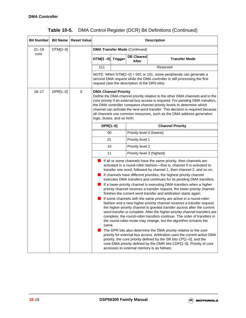
DMA Controller
21–19cont.
DTM[2–0] DMA Transfer Mode (Continued)
DTM[2 –0] TriggerDE Cleared
AfterTransfer Mode
111 Reserved
NOTE: When DTM[2–0] = 001 or 101, some peripherals can generate a second DMA request while the DMA controller is still processing the first request (see the description of the DRS bits).
18–17 DPR[1–0] 0 DMA Channel PriorityDefine the DMA channel priority relative to the other DMA channels and to the core priority if an external bus access is required. For pending DMA transfers, the DMA controller compares channel priority levels to determine which channel can activate the next word transfer. This decision is required because all channels use common resources, such as the DMA address generation logic, buses, and so forth.
DPR[1–0] Channel Priority
00 Priority level 0 (lowest)
01 Priority level 1
10 Priority level 2
11 Priority level 3 (highest)
If all or some channels have the same priority, then channels are activated in a round-robin fashion—that is, channel 0 is activated to transfer one word, followed by channel 1, then channel 2, and so on.
If channels have different priorities, the highest priority channel executes DMA transfers and continues for its pending DMA transfers.
If a lower-priority channel is executing DMA transfers when a higher priority channel receives a transfer request, the lower-priority channel finishes the current word transfer and arbitration starts again.
If some channels with the same priority are active in a round-robin fashion and a new higher-priority channel receives a transfer request, the higher-priority channel is granted transfer access after the current word transfer is complete. After the higher-priority channel transfers are complete, the round-robin transfers continue. The order of transfers in the round-robin mode may change, but the algorithm remains the same.
The DPR bits also determine the DMA priority relative to the core priority for external bus access. Arbitration uses the current active DMA priority, the core priority defined by the SR bits CP[1–0], and the core-DMA priority defined by the OMR bits CDP[1–0]. Priority of core accesses to external memory is as follows:
Table 10-5. DMA Control Register (DCR) Bit Definitions (Continued)
Bit Number Bit Name Reset Value Description
10-18 DSP56300 Family Manual
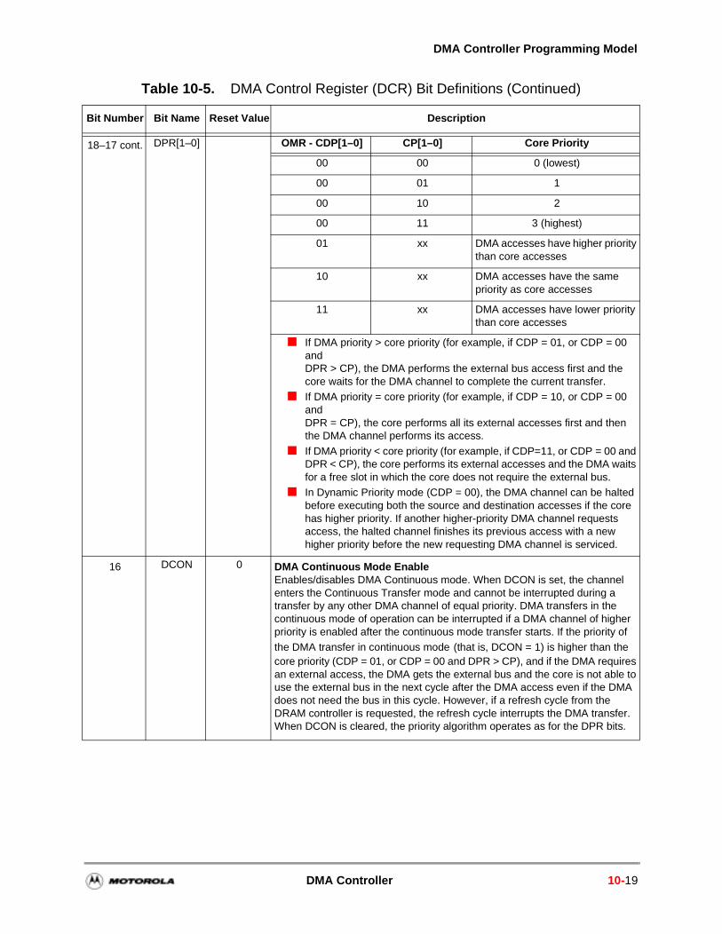
DMA Controller Programming Model
18–17 cont. DPR[1–0] OMR - CDP[1–0] CP[1–0] Core Priority
00 00 0 (lowest)
00 01 1
00 10 2
00 11 3 (highest)
01 xx DMA accesses have higher priority than core accesses
10 xx DMA accesses have the same priority as core accesses
11 xx DMA accesses have lower priority than core accesses
If DMA priority > core priority (for example, if CDP = 01, or CDP = 00 and DPR > CP), the DMA performs the external bus access first and the core waits for the DMA channel to complete the current transfer.
If DMA priority = core priority (for example, if CDP = 10, or CDP = 00 and DPR = CP), the core performs all its external accesses first and then the DMA channel performs its access.
If DMA priority < core priority (for example, if CDP=11, or CDP = 00 and DPR < CP), the core performs its external accesses and the DMA waits for a free slot in which the core does not require the external bus.
In Dynamic Priority mode (CDP = 00), the DMA channel can be halted before executing both the source and destination accesses if the core has higher priority. If another higher-priority DMA channel requests access, the halted channel finishes its previous access with a new higher priority before the new requesting DMA channel is serviced.
16 DCON 0 DMA Continuous Mode Enable Enables/disables DMA Continuous mode. When DCON is set, the channel enters the Continuous Transfer mode and cannot be interrupted during a transfer by any other DMA channel of equal priority. DMA transfers in the continuous mode of operation can be interrupted if a DMA channel of higher priority is enabled after the continuous mode transfer starts. If the priority of the DMA transfer in continuous mode (that is, DCON = 1) is higher than the core priority (CDP = 01, or CDP = 00 and DPR > CP), and if the DMA requires an external access, the DMA gets the external bus and the core is not able to use the external bus in the next cycle after the DMA access even if the DMA does not need the bus in this cycle. However, if a refresh cycle from the DRAM controller is requested, the refresh cycle interrupts the DMA transfer. When DCON is cleared, the priority algorithm operates as for the DPR bits.
Table 10-5. DMA Control Register (DCR) Bit Definitions (Continued)
Bit Number Bit Name Reset Value Description
DMA Controller 10-19
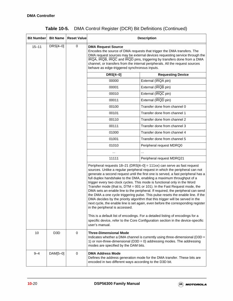
DMA Controller
15–11 DRS[4–0] 0 DMA Request SourceEncodes the source of DMA requests that trigger the DMA transfers. The DMA request sources may be external devices requesting service through the IRQA, IRQB, IRQC and IRQD pins, triggering by transfers done from a DMA channel, or transfers from the internal peripherals. All the request sources behave as edge-triggered synchronous inputs.
DRS[4–0] Requesting Device
00000 External (IRQA pin)
00001 External (IRQB pin)
00010 External (IRQC pin)
00011 External (IRQD pin)
00100 Transfer done from channel 0
00101 Transfer done from channel 1
00110 Transfer done from channel 2
00111 Transfer done from channel 3
01000 Transfer done from channel 4
01001 Transfer done from channel 5
01010 Peripheral request MDRQ0
... ...
11111 Peripheral request MDRQ21
Peripheral requests 18–21 (DRS[4–0] = 111xx) can serve as fast request sources. Unlike a regular peripheral request in which the peripheral can not generate a second request until the first one is served, a fast peripheral has a full duplex handshake to the DMA, enabling a maximum throughput of a trigger every two clock cycles. This mode is functional only in the Word Transfer mode (that is, DTM = 001 or 101). In the Fast Request mode, the DMA sets an enable line to the peripheral. If required, the peripheral can send the DMA a one cycle triggering pulse. This pulse resets the enable line. If the DMA decides by the priority algorithm that this trigger will be served in the next cycle, the enable line is set again, even before the corresponding register in the peripheral is accessed.
This is a default list of encodings. For a detailed listing of encodings for a specific device, refer to the Core Configuration section in the device-specific user’s manual.
10 D3D 0 Three-Dimensional ModeIndicates whether a DMA channel is currently using three-dimensional (D3D = 1) or non-three-dimensional (D3D = 0) addressing modes. The addressing modes are specified by the DAM bits.
9–4 DAM[5–0] 0 DMA Address ModeDefines the address generation mode for the DMA transfer. These bits are encoded in two different ways according to the D3D bit.
Table 10-5. DMA Control Register (DCR) Bit Definitions (Continued)
Bit Number Bit Name Reset Value Description
10-20 DSP56300 Family Manual
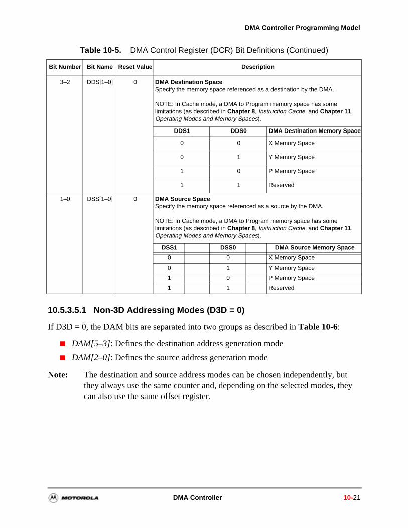
DMA Controller Programming Model
10.5.3.5.1 Non-3D Addressing Modes (D3D = 0)
If D3D = 0, the DAM bits are separated into two groups as described in Table 10-6:
DAM[5–3]: Defines the destination address generation mode
DAM[2–0]: Defines the source address generation mode
Note: The destination and source address modes can be chosen independently, but they always use the same counter and, depending on the selected modes, they can also use the same offset register.
3–2 DDS[1–0] 0 DMA Destination SpaceSpecify the memory space referenced as a destination by the DMA.
NOTE: In Cache mode, a DMA to Program memory space has some limitations (as described in Chapter 8, Instruction Cache, and Chapter 11, Operating Modes and Memory Spaces).
DDS1 DDS0 DMA Destination Memory Space
0 0 X Memory Space
0 1 Y Memory Space
1 0 P Memory Space
1 1 Reserved
1–0 DSS[1–0] 0 DMA Source SpaceSpecify the memory space referenced as a source by the DMA.
NOTE: In Cache mode, a DMA to Program memory space has some limitations (as described in Chapter 8, Instruction Cache, and Chapter 11, Operating Modes and Memory Spaces).
DSS1 DSS0 DMA Source Memory Space
0 0 X Memory Space
0 1 Y Memory Space
1 0 P Memory Space
1 1 Reserved
Table 10-5. DMA Control Register (DCR) Bit Definitions (Continued)
Bit Number Bit Name Reset Value Description
DMA Controller 10-21
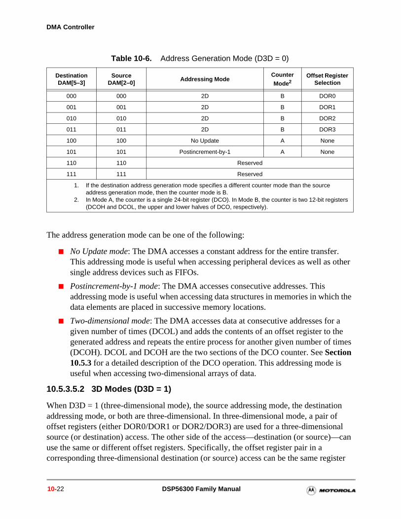
DMA Controller
)—can
gister
The address generation mode can be one of the following:
No Update mode: The DMA accesses a constant address for the entire transfer. This addressing mode is useful when accessing peripheral devices as well as other single address devices such as FIFOs.
Postincrement-by-1 mode: The DMA accesses consecutive addresses. This addressing mode is useful when accessing data structures in memories in which the data elements are placed in successive memory locations.
Two-dimensional mode: The DMA accesses data at consecutive addresses for a given number of times (DCOL) and adds the contents of an offset register to the generated address and repeats the entire process for another given number of times (DCOH). DCOL and DCOH are the two sections of the DCO counter. See Section 10.5.3 for a detailed description of the DCO operation. This addressing mode is useful when accessing two-dimensional arrays of data.
10.5.3.5.2 3D Modes (D3D = 1)
When D3D = 1 (three-dimensional mode), the source addressing mode, the destination addressing mode, or both are three-dimensional. In three-dimensional mode, a pair of offset registers (either DOR0/DOR1 or DOR2/DOR3) are used for a three-dimensional source (or destination) access. The other side of the access—destination (or sourceuse the same or different offset registers. Specifically, the offset register pair in a corresponding three-dimensional destination (or source) access can be the same re
Table 10-6. Address Generation Mode (D3D = 0)
Destination DAM[5–3]
Source DAM[2–0]
Addressing ModeCounter
Mode2Offset Register
Selection
000 000 2D B DOR0
001 001 2D B DOR1
010 010 2D B DOR2
011 011 2D B DOR3
100 100 No Update A None
101 101 Postincrement-by-1 A None
110 110 Reserved
111 111 Reserved
1. If the destination address generation mode specifies a different counter mode than the source address generation mode, then the counter mode is B.
2. In Mode A, the counter is a single 24-bit register (DCO). In Mode B, the counter is two 12-bit registers (DCOH and DCOL, the upper and lower halves of DCO, respectively).
10-22 DSP56300 Family Manual
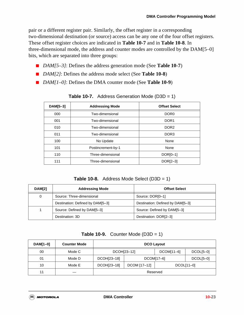
DMA Controller Programming Model
pair or a different register pair. Similarly, the offset register in a corresponding two-dimensional destination (or source) access can be any one of the four offset registers. These offset register choices are indicated in Table 10-7 and in Table 10-8. In three-dimensional mode, the address and counter modes are controlled by the DAM[5–0] bits, which are separated into three groups:
DAM[5–3]: Defines the address generation mode (See Table 10-7)
DAM[2] : Defines the address mode select (See Table 10-8)
DAM[1–0]: Defines the DMA counter mode (See Table 10-9)
Table 10-7. Address Generation Mode (D3D = 1)
DAM[5–3] Addressing Mode Offset Select
000 Two-dimensional DOR0
001 Two-dimensional DOR1
010 Two-dimensional DOR2
011 Two-dimensional DOR3
100 No Update None
101 Postincrement-by-1 None
110 Three-dimensional DOR[0–1]
111 Three-dimensional DOR[2–3]
Table 10-8. Address Mode Select (D3D = 1)
DAM[2] Addressing Mode Offset Select
0 Source: Three-dimensional Source: DOR[0–1]
Destination: Defined by DAM[5–3] Destination: Defined by DAM[5–3]
1 Source: Defined by DAM[5–3] Source: Defined by DAM[5–3]
Destination: 3D Destination: DOR[2–3]
Table 10-9. Counter Mode (D3D = 1)
DAM[1–0] Counter Mode DCO Layout
00 Mode C DCOH[23–12] DCOM[11–6] DCOL[5–0]
01 Mode D DCOH[23–18] DCOM[17–6] DCOL[5–0]
10 Mode E DCOH[23–18] DCOM [17–12] DCOL[11–0]
11 — Reserved
DMA Controller 10-23
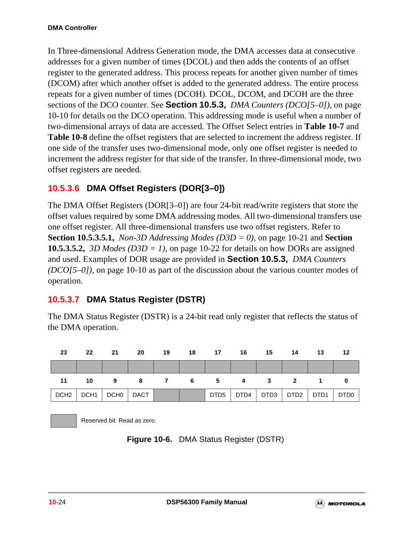
DMA Controller
e s use
d
In Three-dimensional Address Generation mode, the DMA accesses data at consecutive addresses for a given number of times (DCOL) and then adds the contents of an offset register to the generated address. This process repeats for another given number of times (DCOM) after which another offset is added to the generated address. The entire process repeats for a given number of times (DCOH). DCOL, DCOM, and DCOH are the three sections of the DCO counter. See Section 10.5.3, DMA Counters (DCO[5–0]), on page 10-10 for details on the DCO operation. This addressing mode is useful when a number of two-dimensional arrays of data are accessed. The Offset Select entries in Table 10-7 and Table 10-8 define the offset registers that are selected to increment the address register. If one side of the transfer uses two-dimensional mode, only one offset register is needed to increment the address register for that side of the transfer. In three-dimensional mode, two offset registers are needed.
10.5.3.6 DMA Offset Registers (DOR[3–0])
The DMA Offset Registers (DOR[3–0]) are four 24-bit read/write registers that store thoffset values required by some DMA addressing modes. All two-dimensional transferone offset register. All three-dimensional transfers use two offset registers. Refer to Section 10.5.3.5.1, Non-3D Addressing Modes (D3D = 0), on page 10-21 and Section 10.5.3.5.2, 3D Modes (D3D = 1), on page 10-22 for details on how DORs are assigneand used. Examples of DOR usage are provided in Section 10.5.3, DMA Counters (DCO[5–0]), on page 10-10 as part of the discussion about the various counter modes of operation.
10.5.3.7 DMA Status Register (DSTR)
The DMA Status Register (DSTR) is a 24-bit read only register that reflects the status of the DMA operation.
Figure 10-6. DMA Status Register (DSTR)
23 22 21 20 19 18 17 16 15 14 13 12
11 10 9 8 7 6 5 4 3 2 1 0
DCH2 DCH1 DCH0 DACT DTD5 DTD4 DTD3 DTD2 DTD1 DTD0
Reserved bit. Read as zero.
10-24 DSP56300 Family Manual
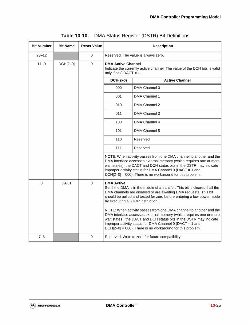
DMA Controller Programming Model
Table 10-10. DMA Status Register (DSTR) Bit Definitions
Bit Number Bit Name Reset Value Description
23–12 0 Reserved. The value is always zero.
11–9 DCH[2–0] 0 DMA Active ChannelIndicate the currently active channel. The value of the DCH bits is valid only if bit 8 DACT = 1.
DCH(2–0) Active Channel
000 DMA Channel 0
001 DMA Channel 1
010 DMA Channel 2
011 DMA Channel 3
100 DMA Channel 4
101 DMA Channel 5
110 Reserved
111 Reserved
NOTE: When activity passes from one DMA channel to another and the DMA interface accesses external memory (which requires one or more wait states), the DACT and DCH status bits in the DSTR may indicate improper activity status for DMA Channel 0 (DACT = 1 and DCH[2–0] = 000). There is no workaround for this problem.
8 DACT 0 DMA Active Set if the DMA is in the middle of a transfer. This bit is cleared if all the DMA channels are disabled or are awaiting DMA requests. This bit should be polled and tested for zero before entering a low power mode by executing a STOP instruction.
NOTE: When activity passes from one DMA channel to another and the DMA interface accesses external memory (which requires one or more wait states), the DACT and DCH status bits in the DSTR may indicate improper activity status for DMA Channel 0 (DACT = 1 and DCH[2–0] = 000). There is no workaround for this problem.
7–6 0 Reserved. Write to zero for future compatibility.
DMA Controller 10-25
DMA Controller
10.6 DMA Restrictions
The following restrictions apply to the DMA operation:
1. Before executing the STOP instruction, poll the DACT status bit until it is read as zero. When the chip enters the Stop state, all previously latched DMA triggers are cleared.
2. The core exits the Wait state when a DMA channel accepts a trigger that is programmed as the selected source trigger. The DMA prevents the core from entering the Wait state if the DMA is active.
3. The DMA Controller can access only the Transmit/Receive Data registers of peripheral interfaces when a source or destination is specified in internal I/O space.
4. If a DMA channel access to external memory is delayed due to bus arbitration or memory wait, the other DMA channels also stop, since the DMA mechanism does not distinguish between the different channels.
5. Depending on the DSP563xx derivative, the internal RAM is divided into banks of either 256 or 1024 words. If the core and the DMA access different banks, they do
5–0 DTD[5–0] 1 DMA Transfer DoneEach DTD bit is assigned for its specific DMA channel (for example, DTD[5] = DMA Channel 5). A DTD bit is set when the last word of a single block transfer is stored in the destination, stopping channel operation. At the same time, the DE bit in the related DCR register may be cleared according to the transfer mode as defined by DTM[2–0]. The last transfer is defined as the one in which the DMA counter reloads its initial value or when software explicitly clears DE. If the related DCR[DIE] bit is set, then the assertion of the DTD bit causes a DMA interrupt request. When the DMA Interrupt is disabled, the core may verify the channel status by polling this bit. The DTD bit for a channel is reset when software sets the DE bit in the corresponding DCR.
NOTES:
Because of pipeline dependencies, after the DCR[DE] bit is set, the corresponding DTDx bit is cleared only after an additional three instruction cycles.
If the DMA channel is in a word transfer mode, clearing DE sets the corresponding DTD bit only after a trigger previously captured by the DMA is handled.
When any DMA channel is set in the infinitive transfer mode (DE is not cleared at end of block) the DTD bit may never be set due to continuous triggering of this channel. However, a DMA interrupt is generated, as defined above, regardless of the DTD bit value.
Table 10-10. DMA Status Register (DSTR) Bit Definitions (Continued)
Bit Number Bit Name Reset Value Description
10-26 DSP56300 Family Manual
DMA Restrictions
ory
nnel
MA
ng the
de, t is t is not
to be
CR
in
not interfere with one another; each continues operations at its maximum speed. If both the core and the DMA access the same bank, then the core has priority and the DMA is delayed until a free slot is available. If the DSP563xx derivative contains an EFCOP, the DMA cannot access the derivative’s lower banks—that is, theDMA cannot access the lower 16 banks (4 K) of the DSP56307 X and Y memor the lower 10 banks (10 K) of the DSP56311 X and Y memory. These lowerbanks are shared between the core and the EFCOP.
6. Write to the DMA Address Registers and the DMA Counter only when the chathat uses them is disabled (DE = 0 and DTD = 1). The operation of the DMA Controller cannot be guaranteed if one of these registers is written while the Dchannel that uses it is busy.
7. A change in the request source should be initiated only when the correspondiDMA channel is idle. If the channel is forced to enter the idle state by clearingDMA Enable (DE) control bit, the corresponding DMA Transfer Done (DTD) status bit should be polled until it is read as ‘1’.
8. If a DMA channel is programmed to perform accesses in the word transfer mothe corresponding DTD status bit is set only after the current captured requesserviced by an appropriate transfer. This ensures that the last captured requeslost.
Note: If the channel priority is low, the DTD is set only when it receives the priorityperform its accesses. In order to shorten this time, the channel priority mayraised before DE is cleared.
9. While a DMA channel is enabled (DE = 1), do not modify any of the channel Dbits, except for the DE bit itself.
10.Due to pipelining, after the DE bit in DCRx is set, the corresponding DTDx bitDSTR is not cleared until after three more instruction cycles.
11.The DMA Controller cannot access GPIO pins.
DMA Controller 10-27

DMA Controller
10-28 DSP56300 Family Manual
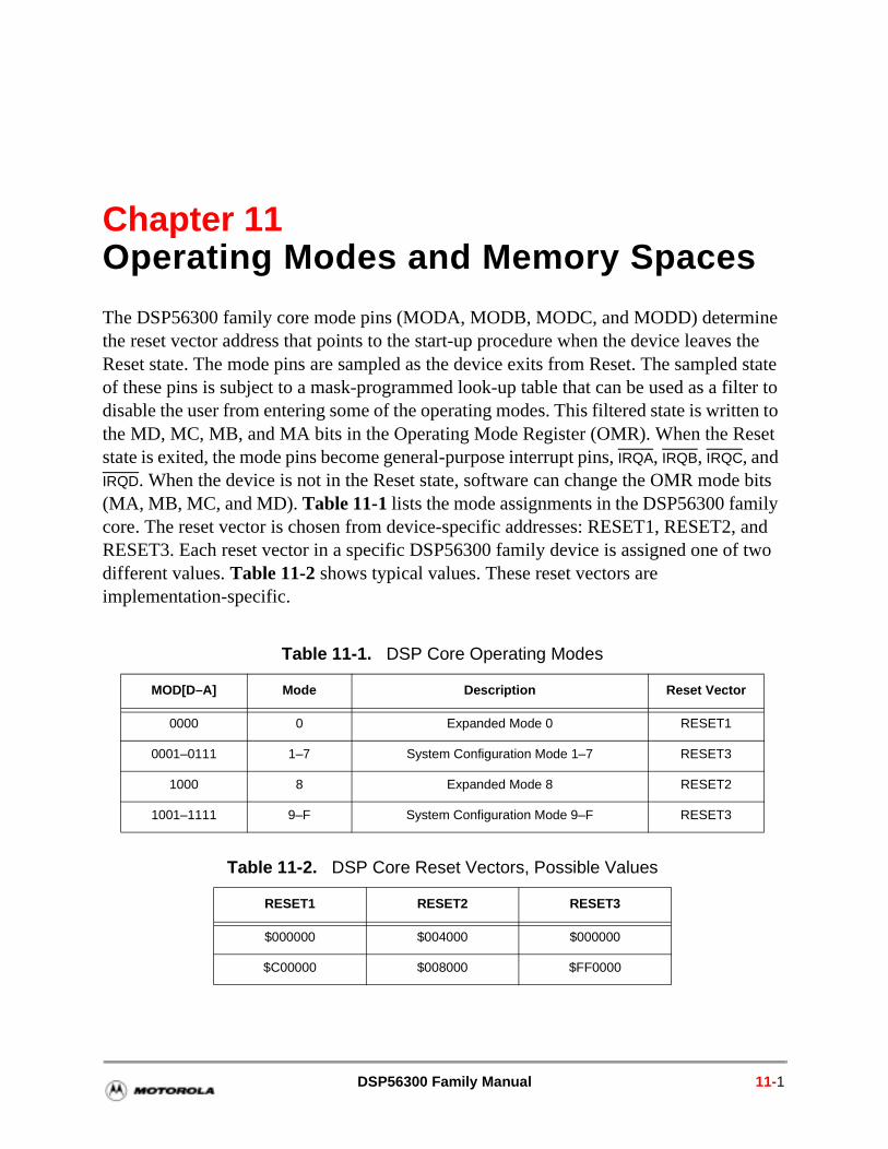
Chapter 11Operating Modes and Memory Spaces
The DSP56300 family core mode pins (MODA, MODB, MODC, and MODD) determine the reset vector address that points to the start-up procedure when the device leaves the Reset state. The mode pins are sampled as the device exits from Reset. The sampled state of these pins is subject to a mask-programmed look-up table that can be used as a filter to disable the user from entering some of the operating modes. This filtered state is written to the MD, MC, MB, and MA bits in the Operating Mode Register (OMR). When the Reset state is exited, the mode pins become general-purpose interrupt pins, IRQA, IRQB, IRQC, and IRQD. When the device is not in the Reset state, software can change the OMR mode bits (MA, MB, MC, and MD). Table 11-1 lists the mode assignments in the DSP56300 family core. The reset vector is chosen from device-specific addresses: RESET1, RESET2, and RESET3. Each reset vector in a specific DSP56300 family device is assigned one of two different values. Table 11-2 shows typical values. These reset vectors are implementation-specific.
Table 11-1. DSP Core Operating Modes
MOD[D–A] Mode Description Reset Vector
0000 0 Expanded Mode 0 RESET1
0001–0111 1–7 System Configuration Mode 1–7 RESET3
1000 8 Expanded Mode 8 RESET2
1001–1111 9–F System Configuration Mode 9–F RESET3
Table 11-2. DSP Core Reset Vectors, Possible Values
RESET1 RESET2 RESET3
$000000 $004000 $000000
$C00000 $008000 $FF0000
DSP56300 Family Manual 11-1
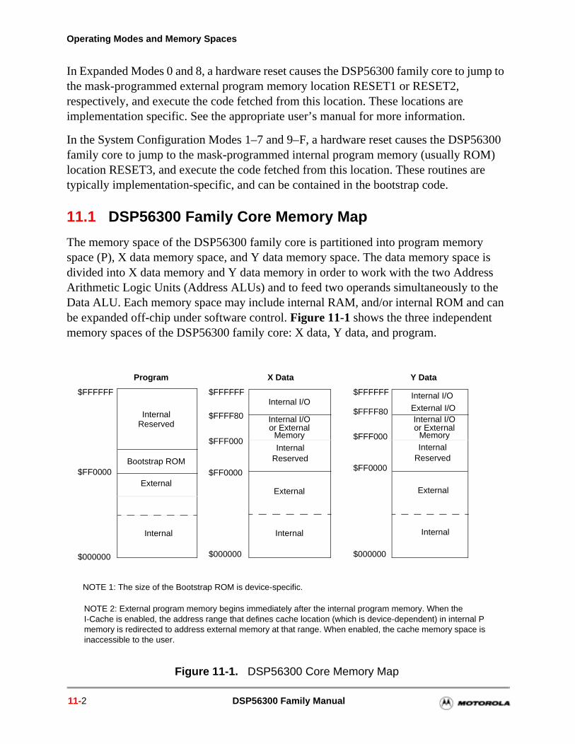
Operating Modes and Memory Spaces
56300 M) re
y ce is ss the can
In Expanded Modes 0 and 8, a hardware reset causes the DSP56300 family core to jump to the mask-programmed external program memory location RESET1 or RESET2, respectively, and execute the code fetched from this location. These locations are implementation specific. See the appropriate user’s manual for more information.
In the System Configuration Modes 1–7 and 9–F, a hardware reset causes the DSPfamily core to jump to the mask-programmed internal program memory (usually ROlocation RESET3, and execute the code fetched from this location. These routines atypically implementation-specific, and can be contained in the bootstrap code.
11.1 DSP56300 Family Core Memory Map
The memory space of the DSP56300 family core is partitioned into program memorspace (P), X data memory space, and Y data memory space. The data memory spadivided into X data memory and Y data memory in order to work with the two AddreArithmetic Logic Units (Address ALUs) and to feed two operands simultaneously to Data ALU. Each memory space may include internal RAM, and/or internal ROM andbe expanded off-chip under software control. Figure 11-1 shows the three independent memory spaces of the DSP56300 family core: X data, Y data, and program.
Figure 11-1. DSP56300 Core Memory Map
Bootstrap ROM
Program
$FFFFFF
$000000
Internal
External
X Data
$FFFFFF
$000000
External
Internal I/O
Y Data
$FFFFFF
$000000
External
Internal I/O
$FFFF80 $FFFF80
Internal Internal
or ExternalInternal I/O
External I/O
$FF0000
InternalReserved
Memoryor ExternalInternal I/O
Memory$FFF000 $FFF000
InternalReserved
InternalReserved
$FF0000 $FF0000
NOTE 1: The size of the Bootstrap ROM is device-specific.
NOTE 2: External program memory begins immediately after the internal program memory. When the I-Cache is enabled, the address range that defines cache location (which is device-dependent) in internal P memory is redirected to address external memory at that range. When enabled, the cache memory space is inaccessible to the user.
11-2 DSP56300 Family Manual
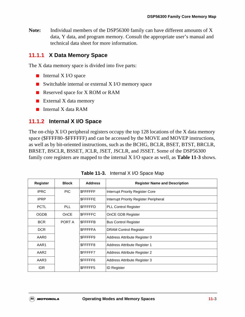
DSP56300 Family Core Memory Map
mory ctions, LR, 0
Note: Individual members of the DSP56300 family can have different amounts of X data, Y data, and program memory. Consult the appropriate user’s manual and technical data sheet for more information.
11.1.1 X Data Memory Space
The X data memory space is divided into five parts:
Internal X I/O space
Switchable internal or external X I/O memory space
Reserved space for X ROM or RAM
External X data memory
Internal X data RAM
11.1.2 Internal X I/O Space
The on-chip X I/O peripheral registers occupy the top 128 locations of the X data mespace ($FFFF80–$FFFFFF) and can be accessed by the MOVE and MOVEP instruas well as by bit-oriented instructions, such as the BCHG, BCLR, BSET, BTST, BRCBRSET, BSCLR, BSSET, JCLR, JSET, JSCLR, and JSSET. Some of the DSP5630family core registers are mapped to the internal X I/O space as well, as Table 11-3 shows.
Table 11-3. Internal X I/O Space Map
Register Block Address Register Name and Description
IPRC PIC $FFFFFF Interrupt Priority Register Core
IPRP $FFFFFE Interrupt Priority Register Peripheral
PCTL PLL $FFFFFD PLL Control Register
OGDB OnCE $FFFFFC OnCE GDB Register
BCR PORT A $FFFFFB Bus Control Register
DCR $FFFFFA DRAM Control Register
AAR0 $FFFFF9 Address Attribute Register 0
AAR1 $FFFFF8 Address Attribute Register 1
AAR2 $FFFFF7 Address Attribute Register 2
AAR3 $FFFFF6 Address Attribute Register 3
IDR $FFFFF5 ID Register
Operating Modes and Memory Spaces 11-3
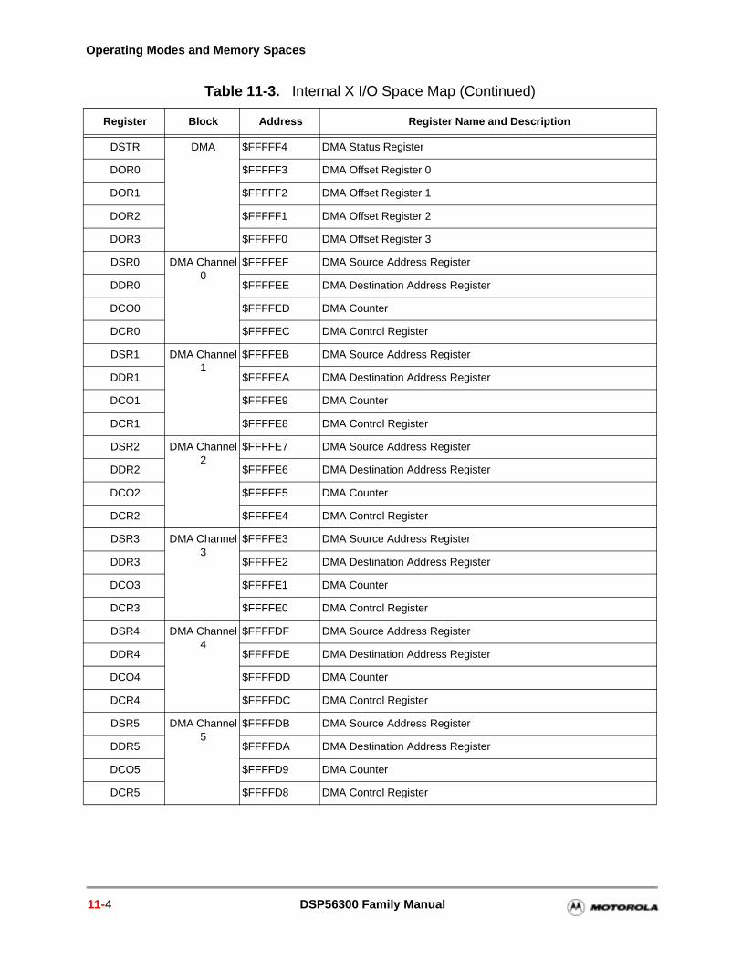
Operating Modes and Memory Spaces
DSTR DMA $FFFFF4 DMA Status Register
DOR0 $FFFFF3 DMA Offset Register 0
DOR1 $FFFFF2 DMA Offset Register 1
DOR2 $FFFFF1 DMA Offset Register 2
DOR3 $FFFFF0 DMA Offset Register 3
DSR0 DMA Channel 0
$FFFFEF DMA Source Address Register
DDR0 $FFFFEE DMA Destination Address Register
DCO0 $FFFFED DMA Counter
DCR0 $FFFFEC DMA Control Register
DSR1 DMA Channel 1
$FFFFEB DMA Source Address Register
DDR1 $FFFFEA DMA Destination Address Register
DCO1 $FFFFE9 DMA Counter
DCR1 $FFFFE8 DMA Control Register
DSR2 DMA Channel 2
$FFFFE7 DMA Source Address Register
DDR2 $FFFFE6 DMA Destination Address Register
DCO2 $FFFFE5 DMA Counter
DCR2 $FFFFE4 DMA Control Register
DSR3 DMA Channel 3
$FFFFE3 DMA Source Address Register
DDR3 $FFFFE2 DMA Destination Address Register
DCO3 $FFFFE1 DMA Counter
DCR3 $FFFFE0 DMA Control Register
DSR4 DMA Channel 4
$FFFFDF DMA Source Address Register
DDR4 $FFFFDE DMA Destination Address Register
DCO4 $FFFFDD DMA Counter
DCR4 $FFFFDC DMA Control Register
DSR5 DMA Channel 5
$FFFFDB DMA Source Address Register
DDR5 $FFFFDA DMA Destination Address Register
DCO5 $FFFFD9 DMA Counter
DCR5 $FFFFD8 DMA Control Register
Table 11-3. Internal X I/O Space Map (Continued)
Register Block Address Register Name and Description
11-4 DSP56300 Family Manual
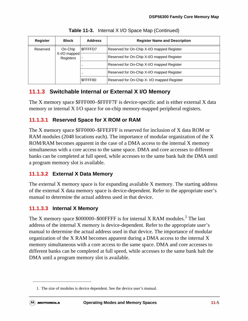
DSP56300 Family Core Memory Map
ta
r X y erent A until
dress user’s
r’s ular es to lt the
11.1.3 Switchable Internal or External X I/O Memory
The X memory space $FFF000–$FFFF7F is device-specific and is either external X damemory or internal X I/O space for on-chip memory-mapped peripheral registers.
11.1.3.1 Reserved Space for X ROM or RAM
The X memory space $FF0000–$FFEFFF is reserved for inclusion of X data ROM oRAM modules (2048 locations each). The importance of modular organization of theROM/RAM becomes apparent in the case of a DMA access to the internal X memorsimultaneous with a core access to the same space. DMA and core accesses to diffbanks can be completed at full speed, while accesses to the same bank halt the DMa program memory slot is available.
11.1.3.2 External X Data Memory
The external X memory space is for expanding available X memory. The starting adof the external X data memory space is device-dependent. Refer to the appropriate manual to determine the actual address used in that device.
11.1.3.3 Internal X Memory
The X memory space $000000–$00FFFF is for internal X RAM modules.1 The last address of the internal X memory is device-dependent. Refer to the appropriate usemanual to determine the actual address used in that device. The importance of modorganization of the X RAM becomes apparent during a DMA access to the internal Xmemory simultaneous with a core access to the same space. DMA and core accessdifferent banks can be completed at full speed, while accesses to the same bank haDMA until a program memory slot is available.
Reserved On-Chip X-I/O mapped
Registers
$FFFFD7 Reserved for On-Chip X-I/O mapped Register
.. Reserved for On-Chip X-I/O mapped Register
.. Reserved for On-Chip X-I/O mapped Register
.. Reserved for On-Chip X-I/O mapped Register
$FFFF80 Reserved for On-Chip X- I/O mapped Register
1. The size of modules is device dependent. See the device user’s manual.
Table 11-3. Internal X I/O Space Map (Continued)
Register Block Address Register Name and Description
Operating Modes and Memory Spaces 11-5
Operating Modes and Memory Spaces
d into nal
data
r Y y erent A until
arting opriate
11.1.4 Y Data Memory Space
The Y data memory space is divided into five parts:
Internal/External Y I/O space
Switchable internal or external Y I/O memory space
Reserved space for Y ROM or RAM
External Y data memory
Internal Y data RAM
11.1.4.1 Internal/External Y I/O Space
The off-chip or on-chip Y I/O peripheral registers occupy the top 128 locations of the Y data memory space ($FFFF80–$FFFFFF) and can be accessed by MOVE and MOVEPinstructions and by bit-oriented instructions (BCHG, BCLR, BSET, BTST, BRCLR, BRSET, BSCLR, BSSET, JCLR, JSET, JSCLR and JSSET). This space is partitioneeight equal parts (16 locations each). Each part is device-specific and is either exterY I/O or internal Y I/O space.
11.1.4.2 Switchable Internal or External Y I/O Memory
The Y memory space $FFF000–$FFFF7F is device-specific and is either external Ymemory or internal Y I/O space for on-chip memory-mapped peripheral registers.
11.1.4.3 Reserved Space for Y ROM or RAM
The Y memory space $FF0000–$FFEFFF is reserved for inclusion of Y data ROM oRAM modules (2048 locations each). The importance of modular organization of theROM/RAM becomes apparent in the case of a DMA access to the internal Y memorsimultaneous with a core access to the same space. DMA and core accesses to diffbanks can be completed at full speed, while accesses to the same bank halt the DMa program memory slot is available.
11.1.4.4 External Y Data Memory
The external Y data memory space is for expanding available Y data memory. The staddress of the external Y data memory space is device-dependent. Refer to the appruser’s manual to determine the actual address used in that device.
11-6 DSP56300 Family Manual
DSP56300 Family Core Memory Map
r’s ular ternal sses to lt the
ialize d some
m
he ase of ame hile
11.1.4.5 Internal Y Memory
The Y memory space $000000–$00FFFF is for internal Y RAM modules.2 The last address of the internal Y memory is device-dependent. Refer to the appropriate usemanual to determine the actual address used in that device. The importance of modorganization of the Y RAM becomes apparent in the case of a DMA access to the inY memory simultaneous with a core access to the same space. DMA and core accedifferent banks can be completed at full speed, while accesses to the same bank haDMA until a program memory slot is available.
11.1.5 Program Memory
The program memory space is divided into five parts:
Bootstrap ROM
Reserved space for Program ROM
External program memory
Internal program memory
Internal instruction cache memory
11.1.5.1 Bootstrap ROM Space
The bootstrap ROM space contains factory programming that allows the DSP to initwhen power is applied. Some DSPs use a 192-word space ($FF0000–$FF00BF) anuse a 3 K words space ($FF0000–$FF0C00). The bootstrap ROM space cannot be accessed by the DMA.
11.1.5.2 Reserved Space for Program ROM
The program memory space $FF00C0–$FFFFFF is reserved for inclusion of PrograROM modules (2048 locations each). Program ROM may be used to contain some operating system program or other application-specific pre-defined user programs. Timportance of modular organization of the Program ROM space is apparent in the cDMA access to the internal program memory simultaneous with core access to the sspace. DMA and core accesses to different banks can be completed at full speed, waccesses to the same bank halt the DMA until a program memory slot is available.
2. The size of modules is device dependent. See the device user’s manual.
Operating Modes and Memory Spaces 11-7
Operating Modes and Memory Spaces
les.
e case to the eed, able. g
dress sabled ared,
ion ace. If its ction
d to
11.1.5.3 External Program Memory
The external program memory space is for expanding internal program memory. The starting address of the external program memory space is device-dependent and also depends on the amount of on-chip Program RAM and the instruction cache size. Refer to the appropriate user’s manual to determine the actual address used in that device.
11.1.5.4 Internal Program Memory
The program memory space $000000–$00FFFF is for internal Program RAM modu3 The last address of the internal program memory is device-dependent. Refer to the appropriate user’s manual to determine the actual address used in that device. Theimportance of modular organization of the program memory becomes apparent in thof a DMA access to the internal program memory simultaneous with a core access same space. DMA and core accesses to different banks can be completed at full spwhile accesses to the same bank halt the DMA until a program memory slot is availThe Program RAM provides a method of changing the program dynamically, allowinefficient overlaying of DSP software algorithms.
11.1.5.5 Internal Instruction Cache RAM
The size of the instruction cache is 1024 24-bit words if it is enabled. The starting adof the instruction cache space is device-dependent. The instruction cache can be diby clearing the Cache Enable (CE) bit in the Status Register (SR). If the CE bit is clethe instruction cache RAM becomes part of the internal Program RAM. The instructcache is used to minimize access time for accesses to external program memory spthe CE bit is set, the instruction is enabled and no longer accessible to the user andaddress space is assigned to external memory. A complete description of the instrucache is provided in Chapter 8, Instruction Cache.
11.2 Sixteen-Bit Compatibility Mode
When the Sixteen Bit Compatibility (SC) mode bit is set, the memory map is changeallow easy access to memory mapped I/O, as described in Figure 11-2.
3. The size of modules is device dependent. See the device user’s manual.
11-8 DSP56300 Family Manual
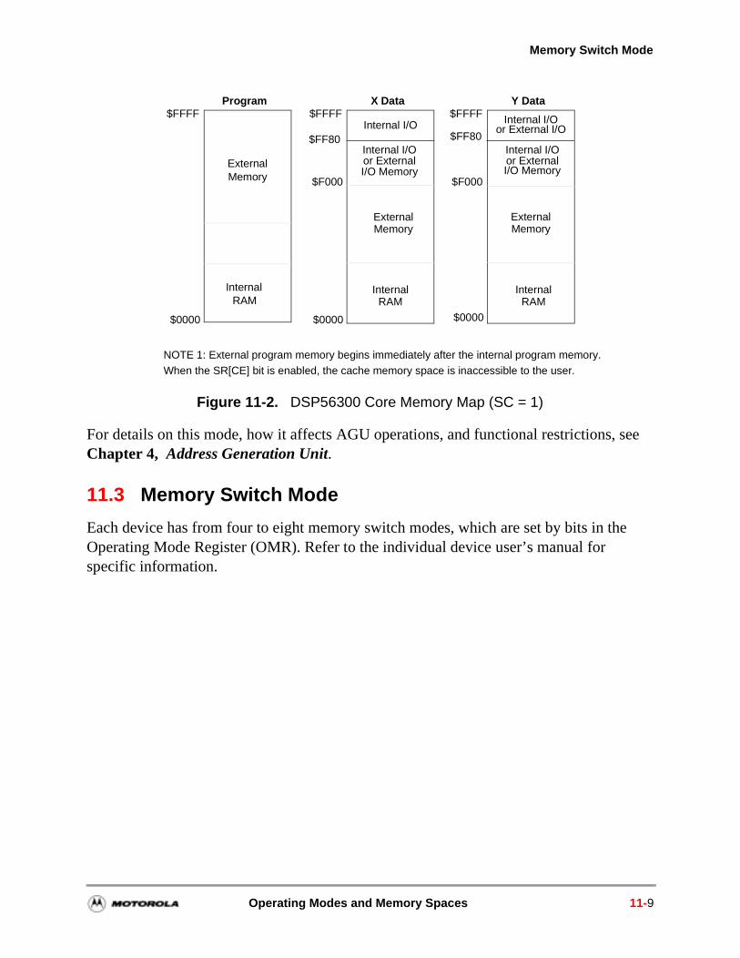
Memory Switch Mode
Figure 11-2. DSP56300 Core Memory Map (SC = 1)
For details on this mode, how it affects AGU operations, and functional restrictions, see Chapter 4, Address Generation Unit.
11.3 Memory Switch Mode
Each device has from four to eight memory switch modes, which are set by bits in the Operating Mode Register (OMR). Refer to the individual device user’s manual for specific information.
Program$FFFF
InternalRAM
External
X Data$FFFF
External
RAM
Internal I/O
Y Data$FFFF
External
Internal I/O
$FF80 $FF80
Memory
Memory Memory
InternalRAM
Internal
or ExternalInternal I/O
or External I/O
I/O Memoryor ExternalInternal I/O
I/O Memory$F000 $F000
$0000 $0000 $0000
NOTE 1: External program memory begins immediately after the internal program memory. When the SR[CE] bit is enabled, the cache memory space is inaccessible to the user.
Operating Modes and Memory Spaces 11-9

Operating Modes and Memory Spaces
11-10 DSP56300 Family Manual
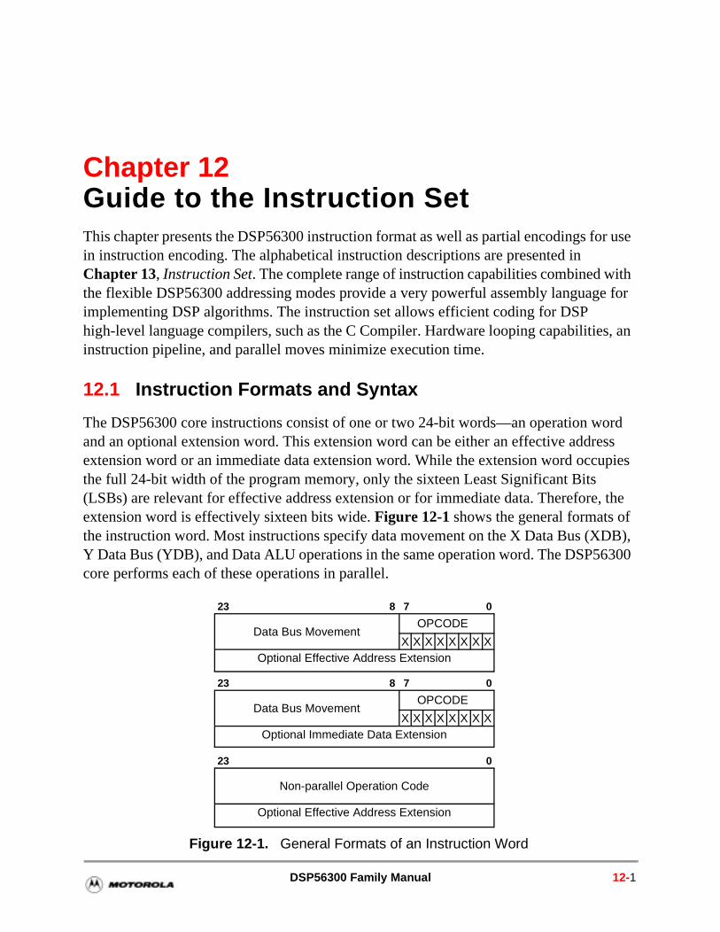
ord ess upies
, the f DB), 6300
Chapter 12Guide to the Instruction SetThis chapter presents the DSP56300 instruction format as well as partial encodings for use in instruction encoding. The alphabetical instruction descriptions are presented in Chapter 13, Instruction Set. The complete range of instruction capabilities combined with the flexible DSP56300 addressing modes provide a very powerful assembly language for implementing DSP algorithms. The instruction set allows efficient coding for DSP high-level language compilers, such as the C Compiler. Hardware looping capabilities, an instruction pipeline, and parallel moves minimize execution time.
12.1 Instruction Formats and Syntax
The DSP56300 core instructions consist of one or two 24-bit words—an operation wand an optional extension word. This extension word can be either an effective addrextension word or an immediate data extension word. While the extension word occthe full 24-bit width of the program memory, only the sixteen Least Significant Bits (LSBs) are relevant for effective address extension or for immediate data. Thereforeextension word is effectively sixteen bits wide. Figure 12-1 shows the general formats othe instruction word. Most instructions specify data movement on the X Data Bus (XY Data Bus (YDB), and Data ALU operations in the same operation word. The DSP5core performs each of these operations in parallel.
Figure 12-1. General Formats of an Instruction Word
Optional Effective Address ExtensionX X X X X X X X
23 8 7 0
Data Bus MovementOPCODE
Optional Immediate Data ExtensionX X X X X X X X
23 8 7 0
Data Bus MovementOPCODE
Optional Effective Address Extension
23 0
Non-parallel Operation Code
DSP56300 Family Manual 12-1
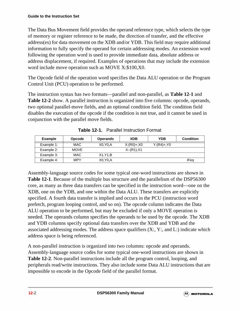
Guide to the Instruction Set
nds,
d in
in 00 on the
a
e XDB
which
in
t are
The Data Bus Movement field provides the operand reference type, which selects the type of memory or register reference to be made, the direction of transfer, and the effective address(es) for data movement on the XDB and/or YDB. This field may require additional information to fully specify the operand for certain addressing modes. An extension word following the operation word is used to provide immediate data, absolute address or address displacement, if required. Examples of operations that may include the extension word include move operation such as MOVE X:$100,X0.
The Opcode field of the operation word specifies the Data ALU operation or the Program Control Unit (PCU) operation to be performed.
The instruction syntax has two formats—parallel and non-parallel, as Table 12-1 and Table 12-2 show. A parallel instruction is organized into five columns: opcode, operatwo optional parallel-move fields, and an optional condition field. The condition field disables the execution of the opcode if the condition is not true, and it cannot be useconjunction with the parallel move fields.
Assembly-language source codes for some typical one-word instructions are shownTable 12-1. Because of the multiple bus structure and the parallelism of the DSP563core, as many as three data transfers can be specified in the instruction word—one XDB, one on the YDB, and one within the Data ALU. These transfers are explicitly specified. A fourth data transfer is implied and occurs in the PCU (instruction word prefetch, program looping control, and so on). The opcode column indicates the DatALU operation to be performed, but may be excluded if only a MOVE operation is needed. The operands column specifies the operands to be used by the opcode. Thand YDB columns specify optional data transfers over the XDB and YDB and the associated addressing modes. The address space qualifiers (X:, Y:, and L:) indicateaddress space is being referenced.
A non-parallel instruction is organized into two columns: opcode and operands. Assembly-language source codes for some typical one-word instructions are shownTable 12-2. Non-parallel instructions include all the program control, looping, and peripherals read/write instructions. They also include some Data ALU instructions thaimpossible to encode in the Opcode field of the parallel format.
Table 12-1. Parallel Instruction Format
Example Opcode Operands XDB YDB Condition
Example 1: MAC X0,Y0,A X:(R0)+,X0 Y:(R4)+,Y0Example 2: MOVE X:-(R1),X1
Example 3: MAC X1,Y1,BExample 4: MPY X0,Y0,A IFeq
12-2 DSP56300 Family Manual
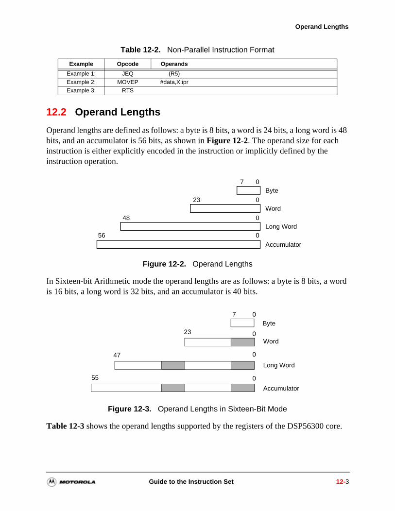
Operand Lengths
12.2 Operand Lengths
Operand lengths are defined as follows: a byte is 8 bits, a word is 24 bits, a long word is 48 bits, and an accumulator is 56 bits, as shown in Figure 12-2. The operand size for each instruction is either explicitly encoded in the instruction or implicitly defined by the instruction operation.
Figure 12-2. Operand Lengths
In Sixteen-bit Arithmetic mode the operand lengths are as follows: a byte is 8 bits, a word is 16 bits, a long word is 32 bits, and an accumulator is 40 bits.
Figure 12-3. Operand Lengths in Sixteen-Bit Mode
Table 12-3 shows the operand lengths supported by the registers of the DSP56300 core.
Table 12-2. Non-Parallel Instruction Format
Example Opcode Operands
Example 1: JEQ (R5)
Example 2: MOVEP #data,X:iprExample 3: RTS
7Byte
Word
Long Word
Accumulator
0
023
048
056
Byte
Word
Long Word
Accumulator
7 0
23 0
0
0
47
55
Guide to the Instruction Set 12-3
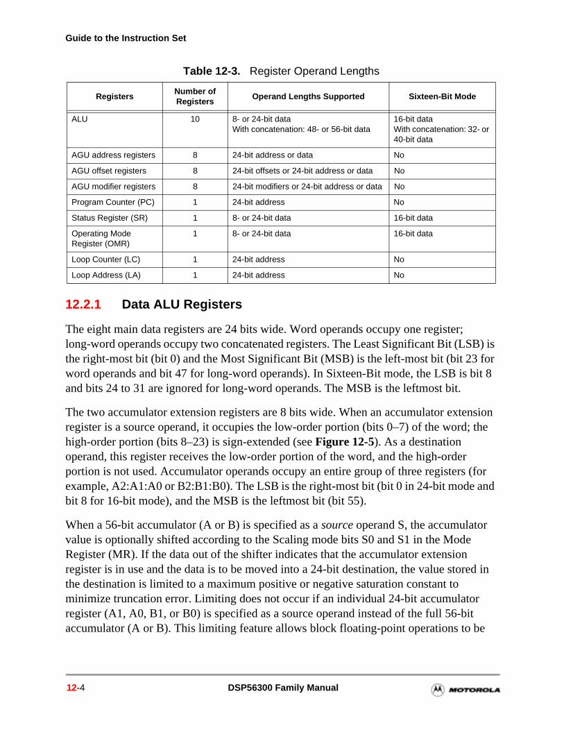
Guide to the Instruction Set
(for nd
ed in
t e
12.2.1 Data ALU Registers
The eight main data registers are 24 bits wide. Word operands occupy one register; long-word operands occupy two concatenated registers. The Least Significant Bit (LSB) is the right-most bit (bit 0) and the Most Significant Bit (MSB) is the left-most bit (bit 23 for word operands and bit 47 for long-word operands). In Sixteen-Bit mode, the LSB is bit 8 and bits 24 to 31 are ignored for long-word operands. The MSB is the leftmost bit.
The two accumulator extension registers are 8 bits wide. When an accumulator extension register is a source operand, it occupies the low-order portion (bits 0–7) of the word; the high-order portion (bits 8–23) is sign-extended (see Figure 12-5). As a destination operand, this register receives the low-order portion of the word, and the high-orderportion is not used. Accumulator operands occupy an entire group of three registersexample, A2:A1:A0 or B2:B1:B0). The LSB is the right-most bit (bit 0 in 24-bit mode abit 8 for 16-bit mode), and the MSB is the leftmost bit (bit 55).
When a 56-bit accumulator (A or B) is specified as a source operand S, the accumulator value is optionally shifted according to the Scaling mode bits S0 and S1 in the ModeRegister (MR). If the data out of the shifter indicates that the accumulator extensionregister is in use and the data is to be moved into a 24-bit destination, the value storthe destination is limited to a maximum positive or negative saturation constant to minimize truncation error. Limiting does not occur if an individual 24-bit accumulatorregister (A1, A0, B1, or B0) is specified as a source operand instead of the full 56-biaccumulator (A or B). This limiting feature allows block floating-point operations to b
Table 12-3. Register Operand Lengths
RegistersNumber of Registers
Operand Lengths Supported Sixteen-Bit Mode
ALU 10 8- or 24-bit dataWith concatenation: 48- or 56-bit data
16-bit dataWith concatenation: 32- or 40-bit data
AGU address registers 8 24-bit address or data No
AGU offset registers 8 24-bit offsets or 24-bit address or data No
AGU modifier registers 8 24-bit modifiers or 24-bit address or data No
Program Counter (PC) 1 24-bit address No
Status Register (SR) 1 8- or 24-bit data 16-bit data
Operating Mode Register (OMR)
1 8- or 24-bit data 16-bit data
Loop Counter (LC) 1 24-bit address No
Loop Address (LA) 1 24-bit address No
12-4 DSP56300 Family Manual
Operand Lengths
fset isters,
ister
er
are
performed with error detection since the L bit in the Condition Code Register (CCR) is latched.
Figure 12-4. Reading and Writing ALU Extension Registers
When a 56-bit accumulator (A or B) is specified as a destination operand D, any 24-bit source data to be moved into that accumulator is automatically extended to 56 bits by sign-extending the MSB of the source operand (bit 23) and appending the source operand with 24 zeros in the LSBs. For 24-bit source operands, both the automatic sign extension and zeroing features can be disabled by specifying the destination register to be one of the individual 24-bit accumulator registers (A1 or B1).
12.2.2 AGU Registers
The twenty-four 24-bit AGU registers can be accessed as word operands for address, address offset, address modifier, and data storage. The Rn notation designates one of the eight address registers, R[0–7]. The Nn notation designates one of the eight address ofregisters, N[0–7]. The Mn notation designates one of the eight address modifier regM[0––7].
12.2.3 Program Control Registers
Within the 24-bit Operating Mode Register (OMR), the Chip Operating Mode (COM)register occupies the low-order 8 bits, the Extended chip Operating Mode (EOM) regoccupies the middle-order 8 bits, and the System Stack Control Status (SCS) registoccupies the high-order 8 bits. The OMR and the Vector Base Address (VBA) are accessed as word operands; however, not all of their bits are defined. Reserved bitsread as zero and should be written with zero for future compatibility.
Bus
Not UsedLSB ofWord
A2/B2
15
Register A2 and B2 Used as a Destination
Register A2 and B2Used as a Source
Sign Extensionof A2/B2
Contentsof A2/B2
Not Used
78 0
15 78 0
Register A2, B2
Bus
15 78 0
Guide to the Instruction Set 12-5
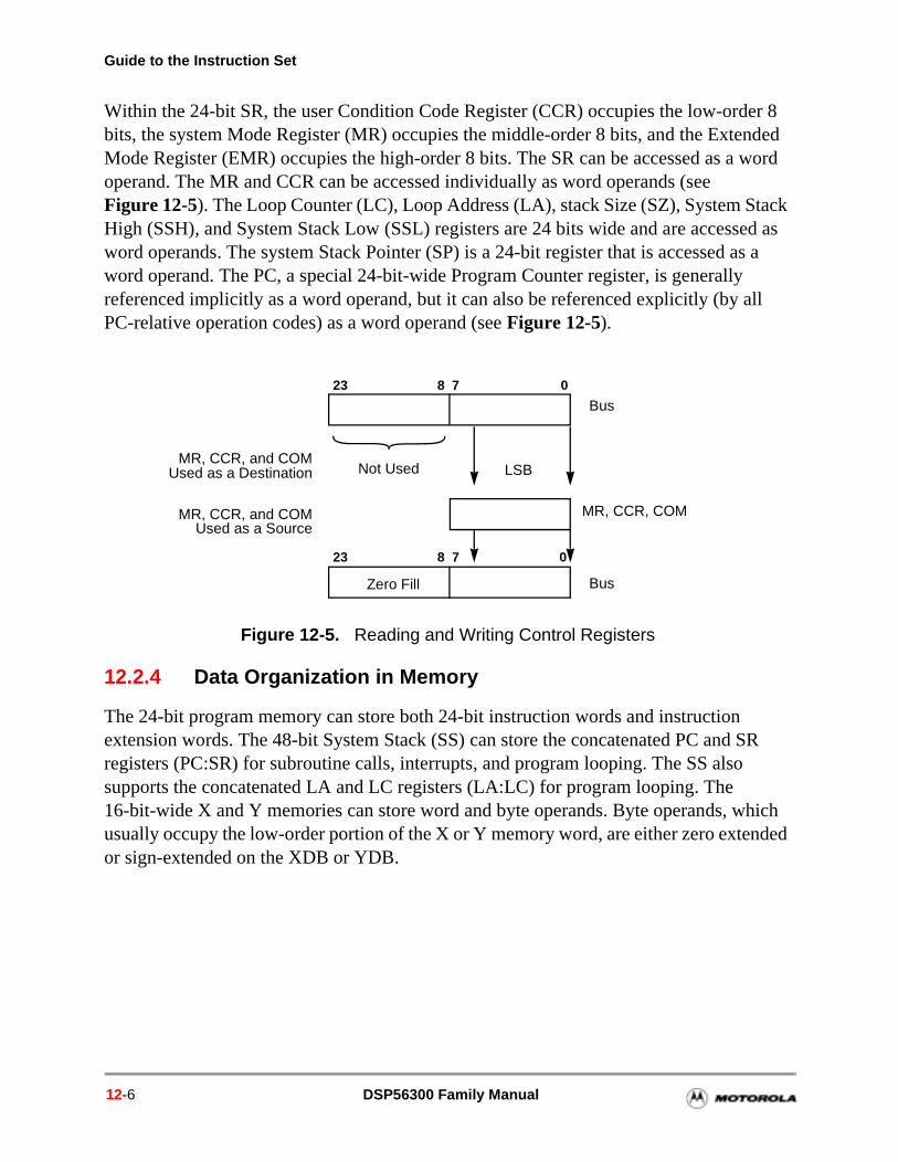
Guide to the Instruction Set
Within the 24-bit SR, the user Condition Code Register (CCR) occupies the low-order 8 bits, the system Mode Register (MR) occupies the middle-order 8 bits, and the Extended Mode Register (EMR) occupies the high-order 8 bits. The SR can be accessed as a word operand. The MR and CCR can be accessed individually as word operands (see Figure 12-5). The Loop Counter (LC), Loop Address (LA), stack Size (SZ), System Stack High (SSH), and System Stack Low (SSL) registers are 24 bits wide and are accessed as word operands. The system Stack Pointer (SP) is a 24-bit register that is accessed as a word operand. The PC, a special 24-bit-wide Program Counter register, is generally referenced implicitly as a word operand, but it can also be referenced explicitly (by all PC-relative operation codes) as a word operand (see Figure 12-5).
Figure 12-5. Reading and Writing Control Registers
12.2.4 Data Organization in Memory
The 24-bit program memory can store both 24-bit instruction words and instruction extension words. The 48-bit System Stack (SS) can store the concatenated PC and SR registers (PC:SR) for subroutine calls, interrupts, and program looping. The SS also supports the concatenated LA and LC registers (LA:LC) for program looping. The 16-bit-wide X and Y memories can store word and byte operands. Byte operands, which usually occupy the low-order portion of the X or Y memory word, are either zero extended or sign-extended on the XDB or YDB.
MR, CCR, and COMUsed as a Destination
Used as a SourceMR, CCR, and COM
Bus
Not Used LSB
23 78 0
23 78 0
Bus
MR, CCR, COM
Zero Fill
12-6 DSP56300 Family Manual
Instruction Groups
12.3 Instruction Groups
The instruction set is divided into the following groups:
Arithmetic
Logical
Bit Manipulation
Loop
Move
Program Control
Instruction Cache Control
Each instruction group is described in the following paragraphs. See Chapter 13, Instruction Set, for a description of each instruction.
12.3.1 Arithmetic Instructions
The arithmetic instructions perform all of the arithmetic operations within the Data ALU. These instructions may affect all of the CCR bits. Arithmetic instructions are register-based (register direct addressing modes used for operands), so that the Data ALU operation indicated by the instruction does not use the XDB, the YDB, or the Global Data Bus (GDB). Optional data transfers may be specified with most arithmetic instructions, which allows for parallel data movement over the XDB and YDB or over the GDB during a Data ALU operation. This parallel movement allows new data to be prefetched for use in subsequent instructions and results calculated in previous instructions to be stored. The move operation that can be specified in parallel to the instruction marked is one of the parallel instructions listed in Table 12-8, Move Instructions, on page 12-12. Arithmetic instructions can be executed conditionally, based on the condition codes generated by the previous instructions. Conditional arithmetic instructions do not allow parallel data movement over the various data buses. Table 12-4 lists the arithmetic instructions.
Table 12-4. Arithmetic Instructions
Mnemonic DescriptionParallel
Instruction*
* A √ in the “Parallel Instruction” column means that the instruction is a parallel instruction. A blank table cell indicates that the instruction is not a parallel instruction.
ABS Absolute Value √
ADC Add Long With Carry √
Guide to the Instruction Set 12-7
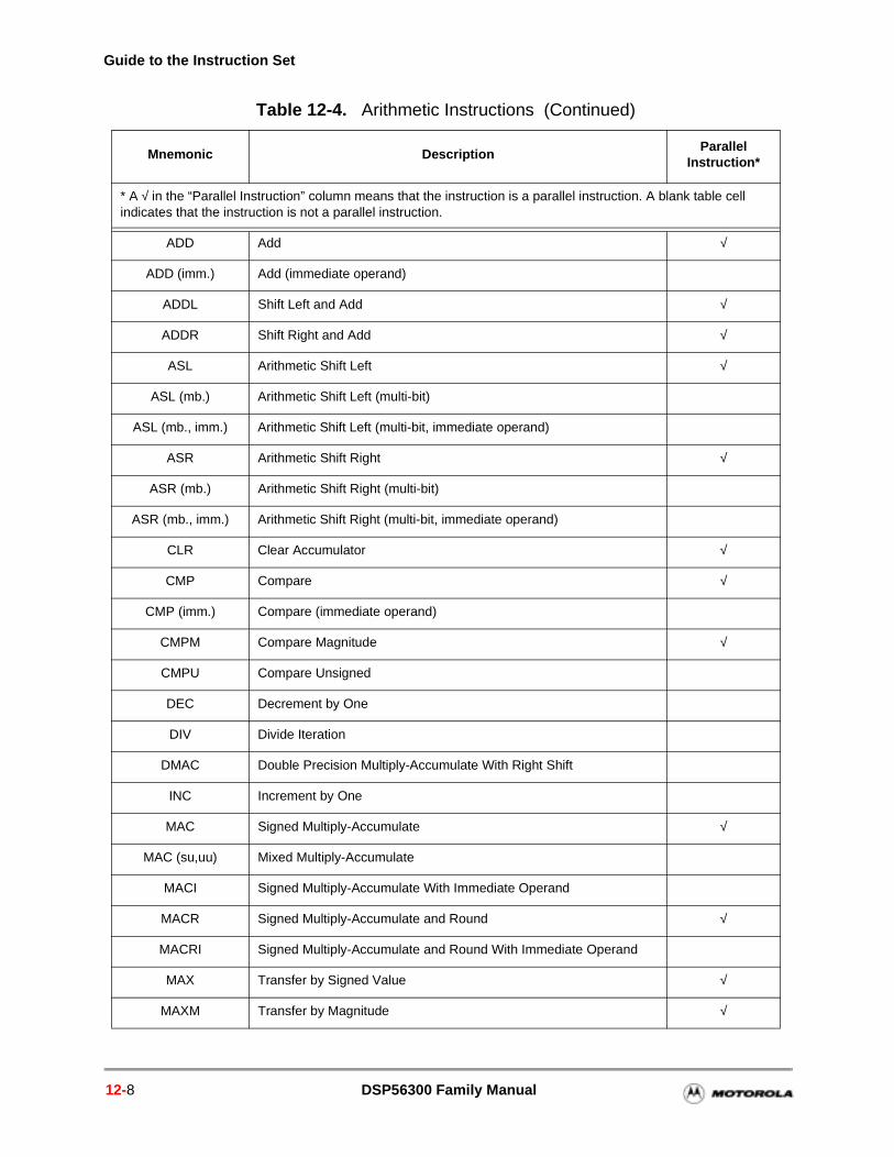
Guide to the Instruction Set
ADD Add √
ADD (imm.) Add (immediate operand)
ADDL Shift Left and Add √
ADDR Shift Right and Add √
ASL Arithmetic Shift Left √
ASL (mb.) Arithmetic Shift Left (multi-bit)
ASL (mb., imm.) Arithmetic Shift Left (multi-bit, immediate operand)
ASR Arithmetic Shift Right √
ASR (mb.) Arithmetic Shift Right (multi-bit)
ASR (mb., imm.) Arithmetic Shift Right (multi-bit, immediate operand)
CLR Clear Accumulator √
CMP Compare √
CMP (imm.) Compare (immediate operand)
CMPM Compare Magnitude √
CMPU Compare Unsigned
DEC Decrement by One
DIV Divide Iteration
DMAC Double Precision Multiply-Accumulate With Right Shift
INC Increment by One
MAC Signed Multiply-Accumulate √
MAC (su,uu) Mixed Multiply-Accumulate
MACI Signed Multiply-Accumulate With Immediate Operand
MACR Signed Multiply-Accumulate and Round √
MACRI Signed Multiply-Accumulate and Round With Immediate Operand
MAX Transfer by Signed Value √
MAXM Transfer by Magnitude √
Table 12-4. Arithmetic Instructions (Continued)
Mnemonic DescriptionParallel
Instruction*
* A √ in the “Parallel Instruction” column means that the instruction is a parallel instruction. A blank table cell indicates that the instruction is not a parallel instruction.
12-8 DSP56300 Family Manual
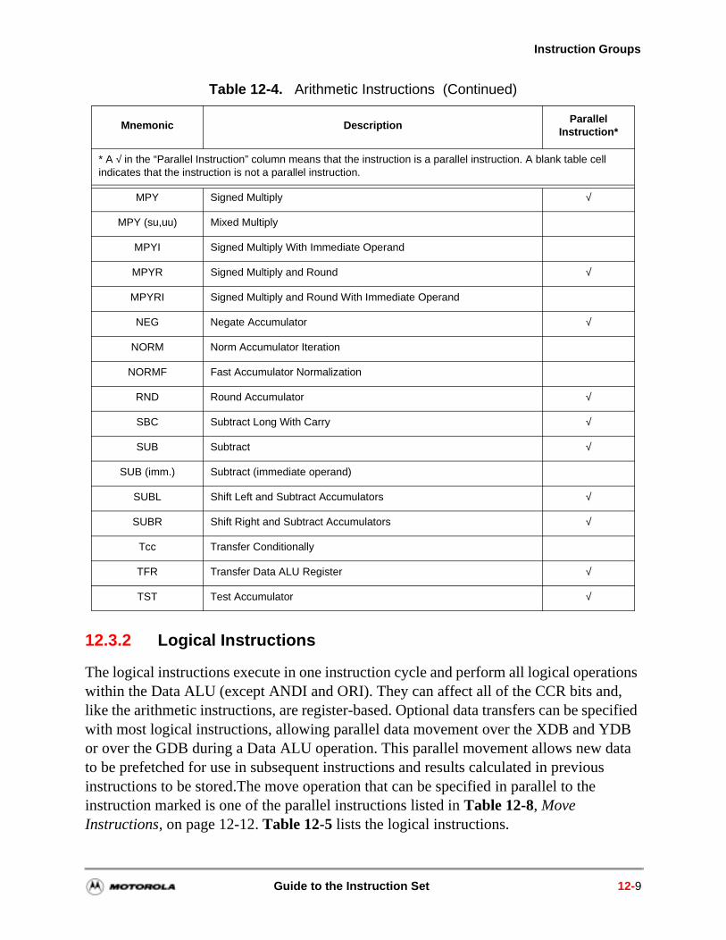
Instruction Groups
12.3.2 Logical Instructions
The logical instructions execute in one instruction cycle and perform all logical operations within the Data ALU (except ANDI and ORI). They can affect all of the CCR bits and, like the arithmetic instructions, are register-based. Optional data transfers can be specified with most logical instructions, allowing parallel data movement over the XDB and YDB or over the GDB during a Data ALU operation. This parallel movement allows new data to be prefetched for use in subsequent instructions and results calculated in previous instructions to be stored.The move operation that can be specified in parallel to the instruction marked is one of the parallel instructions listed in Table 12-8, Move Instructions, on page 12-12. Table 12-5 lists the logical instructions.
MPY Signed Multiply √
MPY (su,uu) Mixed Multiply
MPYI Signed Multiply With Immediate Operand
MPYR Signed Multiply and Round √
MPYRI Signed Multiply and Round With Immediate Operand
NEG Negate Accumulator √
NORM Norm Accumulator Iteration
NORMF Fast Accumulator Normalization
RND Round Accumulator √
SBC Subtract Long With Carry √
SUB Subtract √
SUB (imm.) Subtract (immediate operand)
SUBL Shift Left and Subtract Accumulators √
SUBR Shift Right and Subtract Accumulators √
Tcc Transfer Conditionally
TFR Transfer Data ALU Register √
TST Test Accumulator √
Table 12-4. Arithmetic Instructions (Continued)
Mnemonic DescriptionParallel
Instruction*
* A √ in the “Parallel Instruction” column means that the instruction is a parallel instruction. A blank table cell indicates that the instruction is not a parallel instruction.
Guide to the Instruction Set 12-9
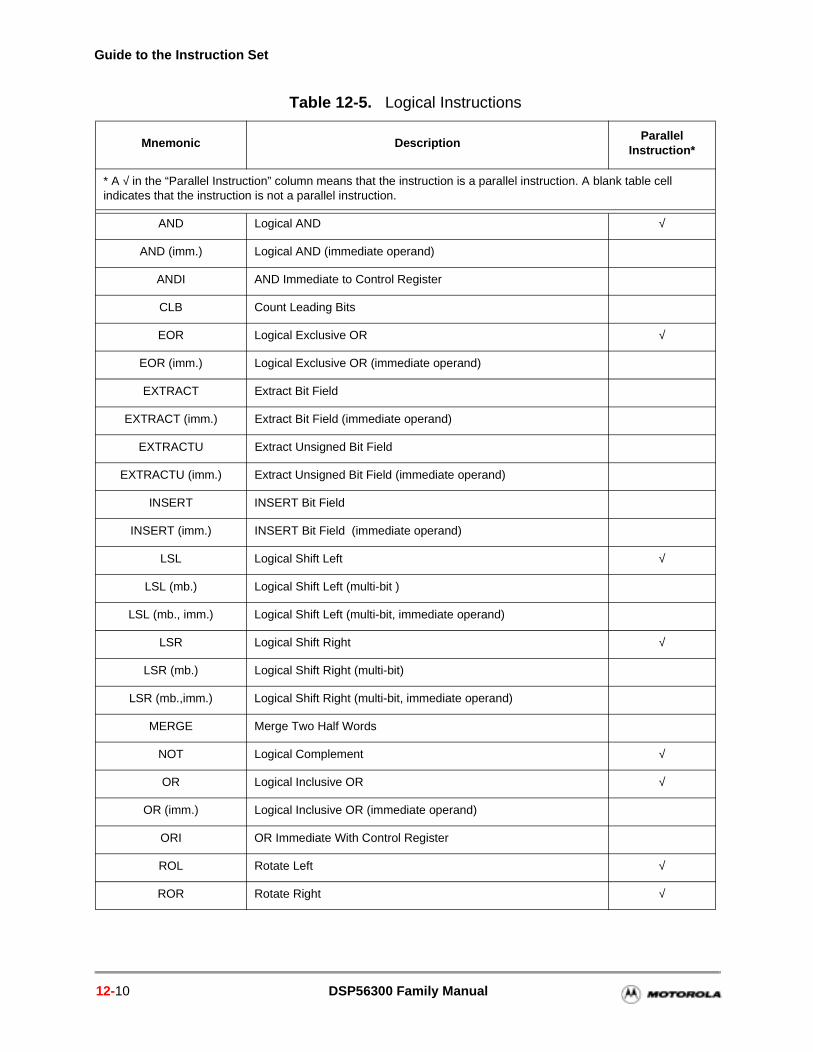
Guide to the Instruction Set
Table 12-5. Logical Instructions
Mnemonic DescriptionParallel
Instruction*
* A √ in the “Parallel Instruction” column means that the instruction is a parallel instruction. A blank table cell indicates that the instruction is not a parallel instruction.
AND Logical AND √
AND (imm.) Logical AND (immediate operand)
ANDI AND Immediate to Control Register
CLB Count Leading Bits
EOR Logical Exclusive OR √
EOR (imm.) Logical Exclusive OR (immediate operand)
EXTRACT Extract Bit Field
EXTRACT (imm.) Extract Bit Field (immediate operand)
EXTRACTU Extract Unsigned Bit Field
EXTRACTU (imm.) Extract Unsigned Bit Field (immediate operand)
INSERT INSERT Bit Field
INSERT (imm.) INSERT Bit Field (immediate operand)
LSL Logical Shift Left √
LSL (mb.) Logical Shift Left (multi-bit )
LSL (mb., imm.) Logical Shift Left (multi-bit, immediate operand)
LSR Logical Shift Right √
LSR (mb.) Logical Shift Right (multi-bit)
LSR (mb.,imm.) Logical Shift Right (multi-bit, immediate operand)
MERGE Merge Two Half Words
NOT Logical Complement √
OR Logical Inclusive OR √
OR (imm.) Logical Inclusive OR (immediate operand)
ORI OR Immediate With Control Register
ROL Rotate Left √
ROR Rotate Right √
12-10 DSP56300 Family Manual
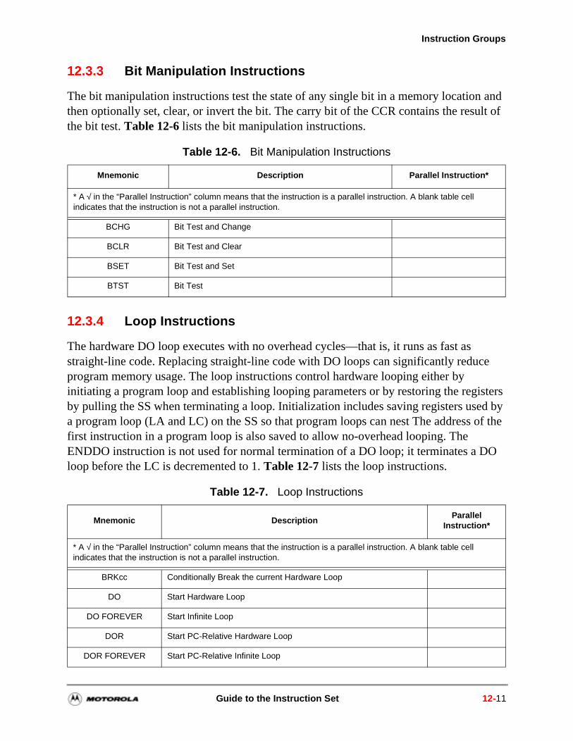
Instruction Groups
e
isters d by of the
O
12.3.3 Bit Manipulation Instructions
The bit manipulation instructions test the state of any single bit in a memory location and then optionally set, clear, or invert the bit. The carry bit of the CCR contains the result of the bit test. Table 12-6 lists the bit manipulation instructions.
12.3.4 Loop Instructions
The hardware DO loop executes with no overhead cycles—that is, it runs as fast asstraight-line code. Replacing straight-line code with DO loops can significantly reducprogram memory usage. The loop instructions control hardware looping either by initiating a program loop and establishing looping parameters or by restoring the regby pulling the SS when terminating a loop. Initialization includes saving registers usea program loop (LA and LC) on the SS so that program loops can nest The addressfirst instruction in a program loop is also saved to allow no-overhead looping. The ENDDO instruction is not used for normal termination of a DO loop; it terminates a Dloop before the LC is decremented to 1. Table 12-7 lists the loop instructions.
Table 12-6. Bit Manipulation Instructions
Mnemonic Description Parallel Instruction*
* A √ in the “Parallel Instruction” column means that the instruction is a parallel instruction. A blank table cell indicates that the instruction is not a parallel instruction.
BCHG Bit Test and Change
BCLR Bit Test and Clear
BSET Bit Test and Set
BTST Bit Test
Table 12-7. Loop Instructions
Mnemonic DescriptionParallel
Instruction*
* A √ in the “Parallel Instruction” column means that the instruction is a parallel instruction. A blank table cell indicates that the instruction is not a parallel instruction.
BRKcc Conditionally Break the current Hardware Loop
DO Start Hardware Loop
DO FOREVER Start Infinite Loop
DOR Start PC-Relative Hardware Loop
DOR FOREVER Start PC-Relative Infinite Loop
Guide to the Instruction Set 12-11
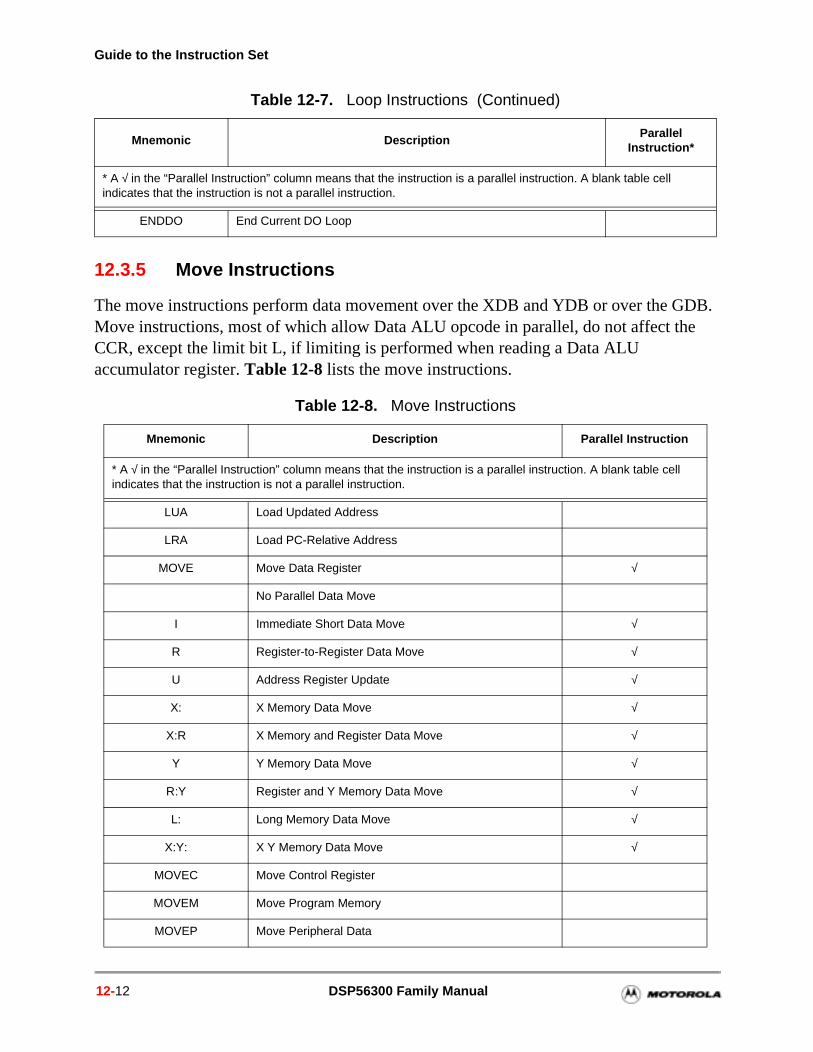
Guide to the Instruction Set
12.3.5 Move Instructions
The move instructions perform data movement over the XDB and YDB or over the GDB. Move instructions, most of which allow Data ALU opcode in parallel, do not affect the CCR, except the limit bit L, if limiting is performed when reading a Data ALU accumulator register. Table 12-8 lists the move instructions.
ENDDO End Current DO Loop
Table 12-8. Move Instructions
Mnemonic Description Parallel Instruction
* A √ in the “Parallel Instruction” column means that the instruction is a parallel instruction. A blank table cell indicates that the instruction is not a parallel instruction.
LUA Load Updated Address
LRA Load PC-Relative Address
MOVE Move Data Register √
No Parallel Data Move
I Immediate Short Data Move √
R Register-to-Register Data Move √
U Address Register Update √
X: X Memory Data Move √
X:R X Memory and Register Data Move √
Y Y Memory Data Move √
R:Y Register and Y Memory Data Move √
L: Long Memory Data Move √
X:Y: X Y Memory Data Move √
MOVEC Move Control Register
MOVEM Move Program Memory
MOVEP Move Peripheral Data
Table 12-7. Loop Instructions (Continued)
Mnemonic DescriptionParallel
Instruction*
* A √ in the “Parallel Instruction” column means that the instruction is a parallel instruction. A blank table cell indicates that the instruction is not a parallel instruction.
12-12 DSP56300 Family Manual
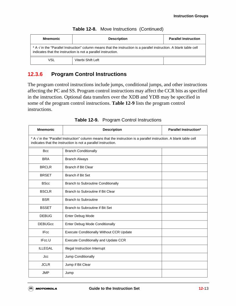
Instruction Groups
12.3.6 Program Control Instructions
The program control instructions include jumps, conditional jumps, and other instructions affecting the PC and SS. Program control instructions may affect the CCR bits as specified in the instruction. Optional data transfers over the XDB and YDB may be specified in some of the program control instructions. Table 12-9 lists the program control instructions.
VSL Viterbi Shift Left
Table 12-9. Program Control Instructions
Mnemonic Description Parallel Instruction*
* A √ in the “Parallel Instruction” column means that the instruction is a parallel instruction. A blank table cell indicates that the instruction is not a parallel instruction.
Bcc Branch Conditionally
BRA Branch Always
BRCLR Branch if Bit Clear
BRSET Branch if Bit Set
BScc Branch to Subroutine Conditionally
BSCLR Branch to Subroutine if Bit Clear
BSR Branch to Subroutine
BSSET Branch to Subroutine if Bit Set
DEBUG Enter Debug Mode
DEBUGcc Enter Debug Mode Conditionally
IFcc Execute Conditionally Without CCR Update
IFcc.U Execute Conditionally and Update CCR
ILLEGAL Illegal Instruction Interrupt
Jcc Jump Conditionally
JCLR Jump if Bit Clear
JMP Jump
Table 12-8. Move Instructions (Continued)
Mnemonic Description Parallel Instruction
* A √ in the “Parallel Instruction” column means that the instruction is a parallel instruction. A blank table cell indicates that the instruction is not a parallel instruction.
Guide to the Instruction Set 12-13
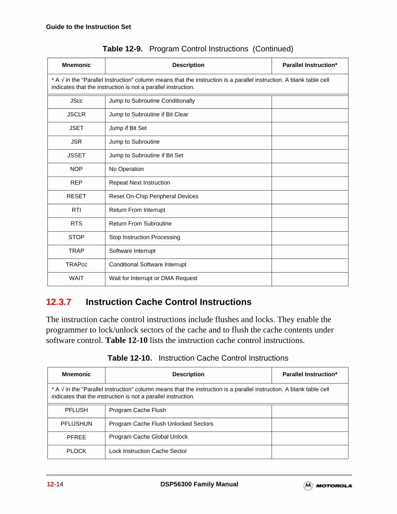
Guide to the Instruction Set
12.3.7 Instruction Cache Control Instructions
The instruction cache control instructions include flushes and locks. They enable the programmer to lock/unlock sectors of the cache and to flush the cache contents under software control. Table 12-10 lists the instruction cache control instructions.
JScc Jump to Subroutine Conditionally
JSCLR Jump to Subroutine if Bit Clear
JSET Jump if Bit Set
JSR Jump to Subroutine
JSSET Jump to Subroutine if Bit Set
NOP No Operation
REP Repeat Next Instruction
RESET Reset On-Chip Peripheral Devices
RTI Return From Interrupt
RTS Return From Subroutine
STOP Stop Instruction Processing
TRAP Software Interrupt
TRAPcc Conditional Software Interrupt
WAIT Wait for Interrupt or DMA Request
Table 12-10. Instruction Cache Control Instructions
Mnemonic Description Parallel Instruction*
* A √ in the “Parallel Instruction” column means that the instruction is a parallel instruction. A blank table cell indicates that the instruction is not a parallel instruction.
PFLUSH Program Cache Flush
PFLUSHUN Program Cache Flush Unlocked Sectors
PFREE Program Cache Global Unlock
PLOCK Lock Instruction Cache Sector
Table 12-9. Program Control Instructions (Continued)
Mnemonic Description Parallel Instruction*
* A √ in the “Parallel Instruction” column means that the instruction is a parallel instruction. A blank table cell indicates that the instruction is not a parallel instruction.
12-14 DSP56300 Family Manual
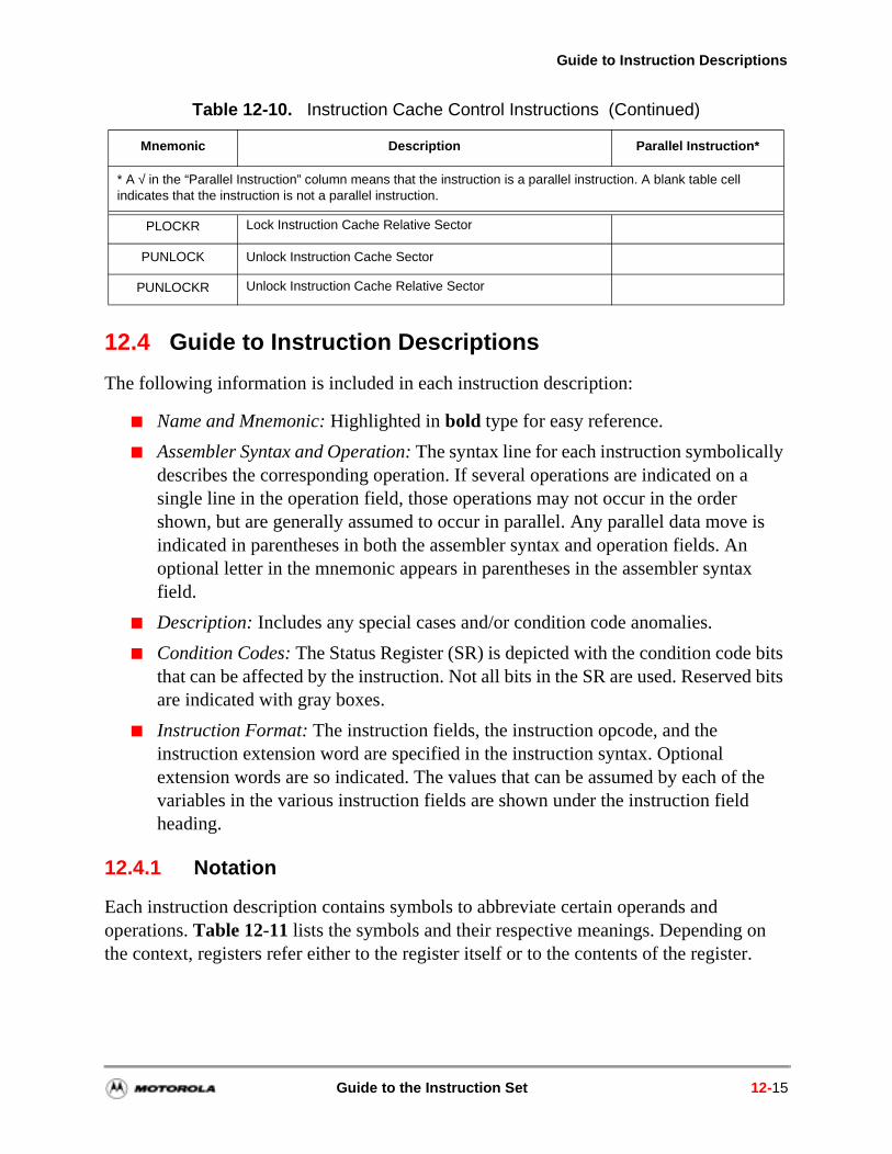
Guide to Instruction Descriptions
12.4 Guide to Instruction Descriptions
The following information is included in each instruction description:
Name and Mnemonic: Highlighted in bold type for easy reference.
Assembler Syntax and Operation: The syntax line for each instruction symbolically describes the corresponding operation. If several operations are indicated on a single line in the operation field, those operations may not occur in the order shown, but are generally assumed to occur in parallel. Any parallel data move is indicated in parentheses in both the assembler syntax and operation fields. An optional letter in the mnemonic appears in parentheses in the assembler syntax field.
Description: Includes any special cases and/or condition code anomalies.
Condition Codes: The Status Register (SR) is depicted with the condition code bits that can be affected by the instruction. Not all bits in the SR are used. Reserved bits are indicated with gray boxes.
Instruction Format: The instruction fields, the instruction opcode, and the instruction extension word are specified in the instruction syntax. Optional extension words are so indicated. The values that can be assumed by each of the variables in the various instruction fields are shown under the instruction field heading.
12.4.1 Notation
Each instruction description contains symbols to abbreviate certain operands and operations. Table 12-11 lists the symbols and their respective meanings. Depending on the context, registers refer either to the register itself or to the contents of the register.
PLOCKR Lock Instruction Cache Relative Sector
PUNLOCK Unlock Instruction Cache Sector
PUNLOCKR Unlock Instruction Cache Relative Sector
Table 12-10. Instruction Cache Control Instructions (Continued)
Mnemonic Description Parallel Instruction*
* A √ in the “Parallel Instruction” column means that the instruction is a parallel instruction. A blank table cell indicates that the instruction is not a parallel instruction.
Guide to the Instruction Set 12-15
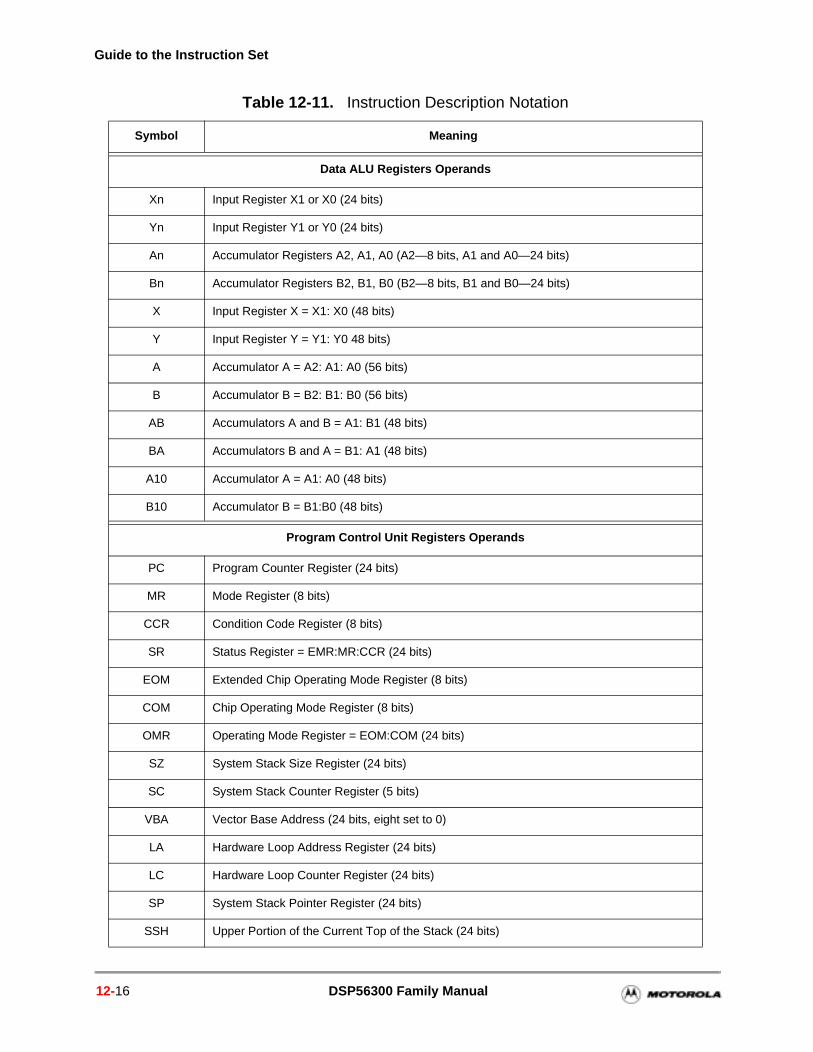
Guide to the Instruction Set
Table 12-11. Instruction Description Notation
Symbol Meaning
Data ALU Registers Operands
Xn Input Register X1 or X0 (24 bits)
Yn Input Register Y1 or Y0 (24 bits)
An Accumulator Registers A2, A1, A0 (A2—8 bits, A1 and A0—24 bits)
Bn Accumulator Registers B2, B1, B0 (B2—8 bits, B1 and B0—24 bits)
X Input Register X = X1: X0 (48 bits)
Y Input Register Y = Y1: Y0 48 bits)
A Accumulator A = A2: A1: A0 (56 bits)
B Accumulator B = B2: B1: B0 (56 bits)
AB Accumulators A and B = A1: B1 (48 bits)
BA Accumulators B and A = B1: A1 (48 bits)
A10 Accumulator A = A1: A0 (48 bits)
B10 Accumulator B = B1:B0 (48 bits)
Program Control Unit Registers Operands
PC Program Counter Register (24 bits)
MR Mode Register (8 bits)
CCR Condition Code Register (8 bits)
SR Status Register = EMR:MR:CCR (24 bits)
EOM Extended Chip Operating Mode Register (8 bits)
COM Chip Operating Mode Register (8 bits)
OMR Operating Mode Register = EOM:COM (24 bits)
SZ System Stack Size Register (24 bits)
SC System Stack Counter Register (5 bits)
VBA Vector Base Address (24 bits, eight set to 0)
LA Hardware Loop Address Register (24 bits)
LC Hardware Loop Counter Register (24 bits)
SP System Stack Pointer Register (24 bits)
SSH Upper Portion of the Current Top of the Stack (24 bits)
12-16 DSP56300 Family Manual
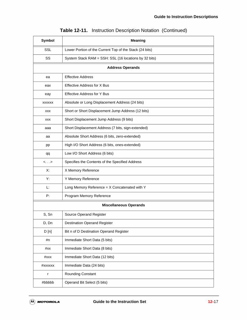
Guide to Instruction Descriptions
SSL Lower Portion of the Current Top of the Stack (24 bits)
SS System Stack RAM = SSH: SSL (16 locations by 32 bits)
Address Operands
ea Effective Address
eax Effective Address for X Bus
eay Effective Address for Y Bus
xxxxxx Absolute or Long Displacement Address (24 bits)
xxx Short or Short Displacement Jump Address (12 bits)
xxx Short Displacement Jump Address (9 bits)
aaa Short Displacement Address (7 bits, sign-extended)
aa Absolute Short Address (6 bits, zero-extended)
pp High I/O Short Address (6 bits, ones-extended)
qq Low I/O Short Address (6 bits)
<. . .> Specifies the Contents of the Specified Address
X: X Memory Reference
Y: Y Memory Reference
L: Long Memory Reference = X Concatenated with Y
P: Program Memory Reference
Miscellaneous Operands
S, Sn Source Operand Register
D, Dn Destination Operand Register
D [n] Bit n of D Destination Operand Register
#n Immediate Short Data (5 bits)
#xx Immediate Short Data (8 bits)
#xxx Immediate Short Data (12 bits)
#xxxxxx Immediate Data (24 bits)
r Rounding Constant
#bbbbb Operand Bit Select (5 bits)
Table 12-11. Instruction Description Notation (Continued)
Symbol Meaning
Guide to the Instruction Set 12-17
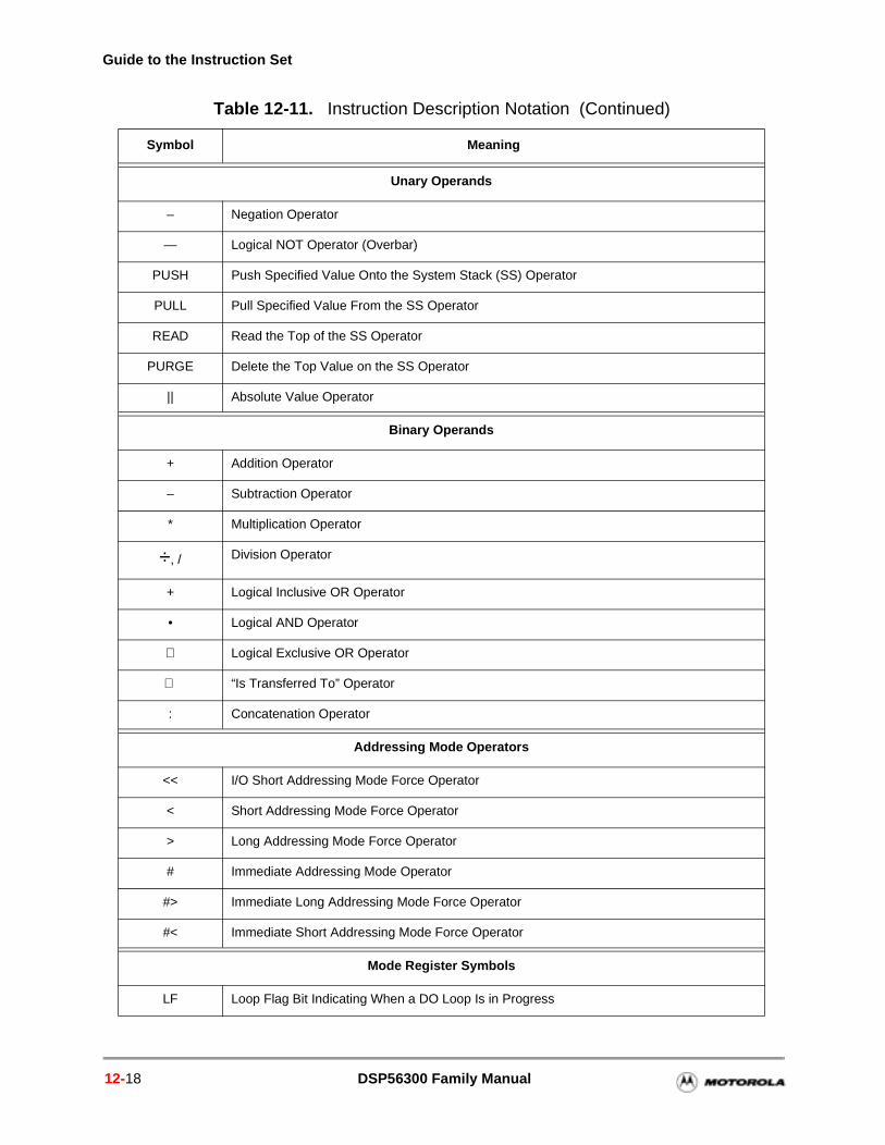
Guide to the Instruction Set
Unary Operands
– Negation Operator
— Logical NOT Operator (Overbar)
PUSH Push Specified Value Onto the System Stack (SS) Operator
PULL Pull Specified Value From the SS Operator
READ Read the Top of the SS Operator
PURGE Delete the Top Value on the SS Operator
|| Absolute Value Operator
Binary Operands
+ Addition Operator
– Subtraction Operator
* Multiplication Operator
÷, / Division Operator
+ Logical Inclusive OR Operator
• Logical AND Operator
⊕ Logical Exclusive OR Operator
⇒ “Is Transferred To” Operator
: Concatenation Operator
Addressing Mode Operators
<< I/O Short Addressing Mode Force Operator
< Short Addressing Mode Force Operator
> Long Addressing Mode Force Operator
# Immediate Addressing Mode Operator
#> Immediate Long Addressing Mode Force Operator
#< Immediate Short Addressing Mode Force Operator
Mode Register Symbols
LF Loop Flag Bit Indicating When a DO Loop Is in Progress
Table 12-11. Instruction Description Notation (Continued)
Symbol Meaning
12-18 DSP56300 Family Manual
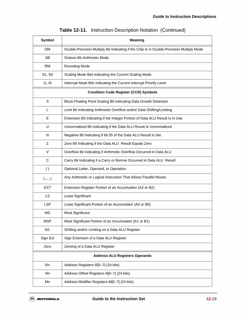
Guide to Instruction Descriptions
DM Double-Precision Multiply Bit Indicating if the Chip Is in Double-Precision Multiply Mode
SB Sixteen-Bit Arithmetic Mode
RM Rounding Mode
S1, S0 Scaling Mode Bits Indicating the Current Scaling Mode
I1, I0 Interrupt Mask Bits Indicating the Current Interrupt Priority Level
Condition Code Register (CCR) Symbols
S Block Floating Point Scaling Bit Indicating Data Growth Detection
L Limit Bit Indicating Arithmetic Overflow and/or Data Shifting/Limiting
E Extension Bit Indicating if the Integer Portion of Data ALU Result Is in Use
U Unnormalized Bit Indicating if the Data ALU Result Is Unnormalized
N Negative Bit Indicating if bit 55 of the Data ALU Result Is Set
Z Zero Bit Indicating if the Data ALU Result Equals Zero
V Overflow Bit Indicating if Arithmetic Overflow Occurred in Data ALU
C Carry Bit Indicating if a Carry or Borrow Occurred in Data ALU Result
( ) Optional Letter, Operand, or Operation
(…) Any Arithmetic or Logical Instruction That Allows Parallel Moves
EXT Extension Register Portion of an Accumulator (A2 or B2)
LS Least Significant
LSP Least Significant Portion of an Accumulator (A0 or B0)
MS Most Significant
MSP Most Significant Portion of an Accumulator (A1 or B1)
S/L Shifting and/or Limiting on a Data ALU Register
Sign Ext Sign Extension of a Data ALU Register
Zero Zeroing of a Data ALU Register
Address ALU Registers Operands
Rn Address Registers R[0–7] (24 bits)
Nn Address Offset Registers N[0–7] (24 bits)
Mn Address Modifier Registers M[0–7] (24 bits)
Table 12-11. Instruction Description Notation (Continued)
Symbol Meaning
Guide to the Instruction Set 12-19
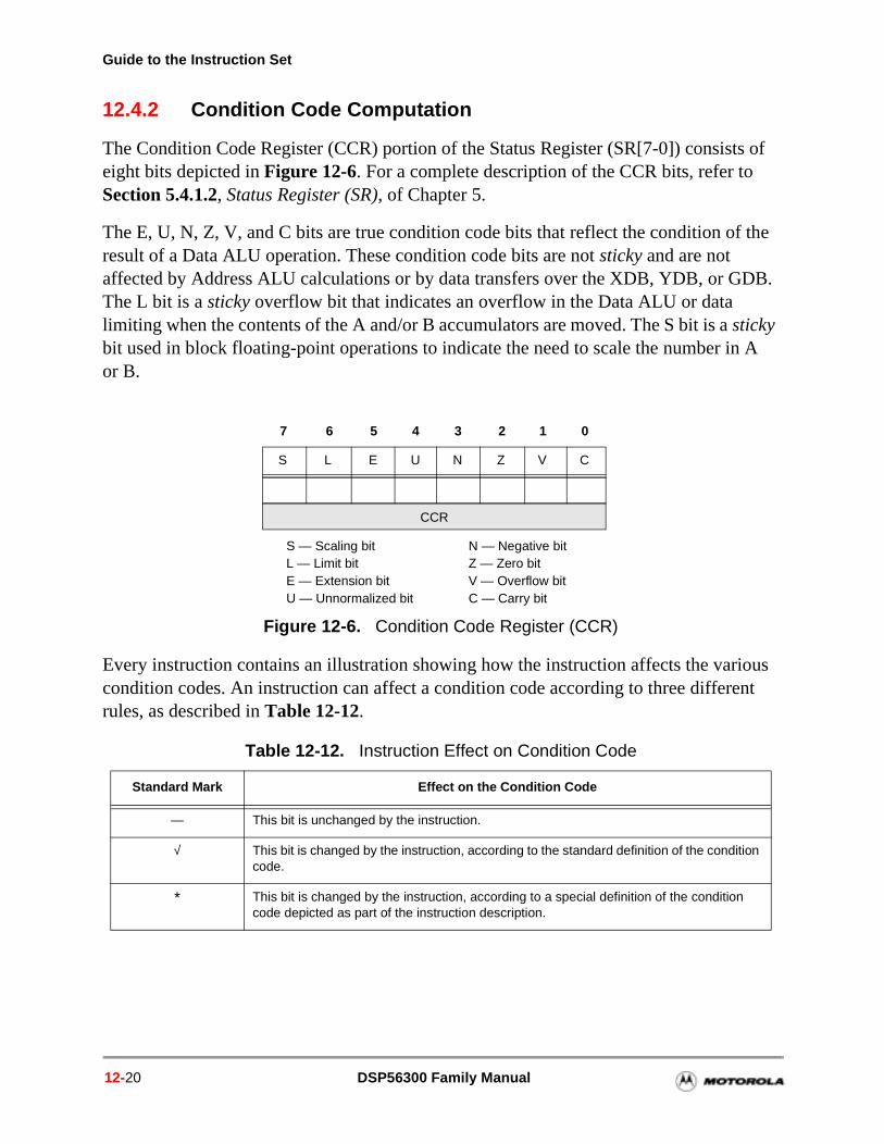
Guide to the Instruction Set
12.4.2 Condition Code Computation
The Condition Code Register (CCR) portion of the Status Register (SR[7-0]) consists of eight bits depicted in Figure 12-6. For a complete description of the CCR bits, refer to Section 5.4.1.2, Status Register (SR), of Chapter 5.
The E, U, N, Z, V, and C bits are true condition code bits that reflect the condition of the result of a Data ALU operation. These condition code bits are not sticky and are not affected by Address ALU calculations or by data transfers over the XDB, YDB, or GDB. The L bit is a sticky overflow bit that indicates an overflow in the Data ALU or data limiting when the contents of the A and/or B accumulators are moved. The S bit is a sticky bit used in block floating-point operations to indicate the need to scale the number in Aor B.
Figure 12-6. Condition Code Register (CCR)
Every instruction contains an illustration showing how the instruction affects the various condition codes. An instruction can affect a condition code according to three different rules, as described in Table 12-12.
Table 12-12. Instruction Effect on Condition Code
Standard Mark Effect on the Condition Code
— This bit is unchanged by the instruction.
√ This bit is changed by the instruction, according to the standard definition of the condition code.
* This bit is changed by the instruction, according to a special definition of the condition code depicted as part of the instruction description.
CCR
S — Scaling bitL — Limit bitE — Extension bitU — Unnormalized bit
N — Negative bitZ — Zero bitV — Overflow bitC — Carry bit
CS L E U N VZ
07 6 5 4 3 12
12-20 DSP56300 Family Manual
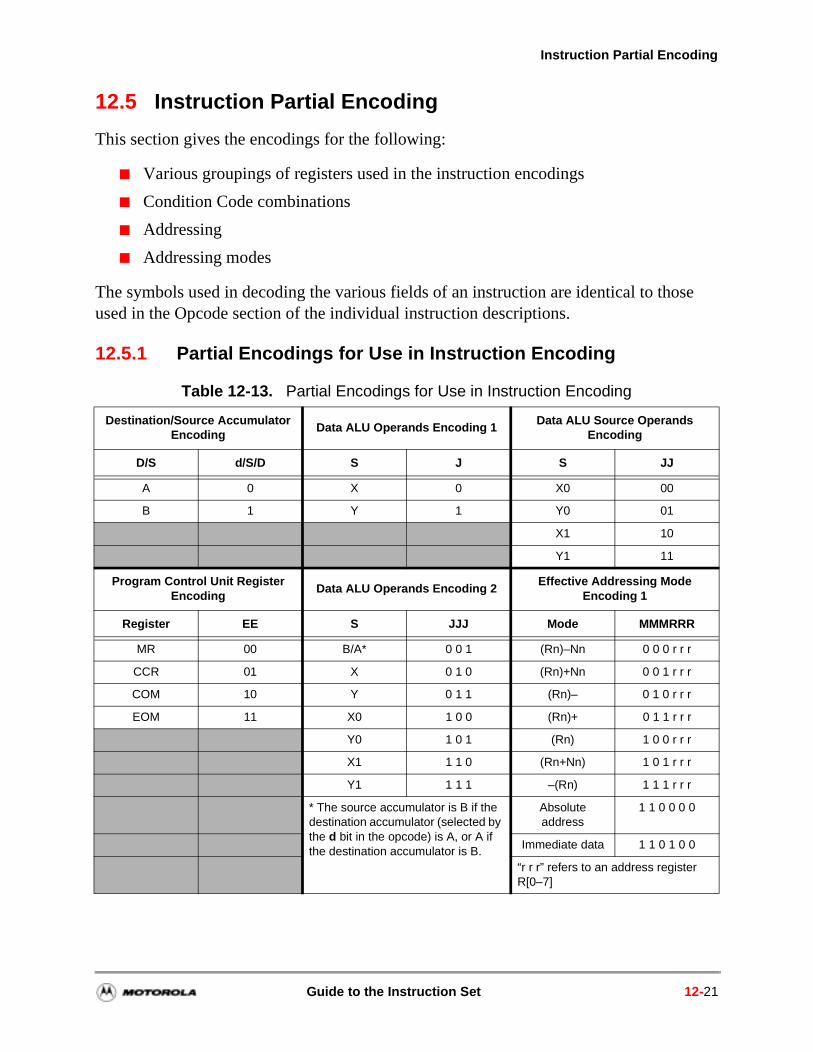
Instruction Partial Encoding
12.5 Instruction Partial Encoding
This section gives the encodings for the following:
Various groupings of registers used in the instruction encodings
Condition Code combinations
Addressing
Addressing modes
The symbols used in decoding the various fields of an instruction are identical to those used in the Opcode section of the individual instruction descriptions.
12.5.1 Partial Encodings for Use in Instruction Encoding
Table 12-13. Partial Encodings for Use in Instruction Encoding
Destination/Source Accumulator Encoding
Data ALU Operands Encoding 1Data ALU Source Operands
Encoding
D/S d/S/D S J S JJ
A 0 X 0 X0 00
B 1 Y 1 Y0 01
X1 10
Y1 11
Program Control Unit Register Encoding
Data ALU Operands Encoding 2Effective Addressing Mode
Encoding 1
Register EE S JJJ Mode MMMRRR
MR 00 B/A* 0 0 1 (Rn)–Nn 0 0 0 r r r
CCR 01 X 0 1 0 (Rn)+Nn 0 0 1 r r r
COM 10 Y 0 1 1 (Rn)– 0 1 0 r r r
EOM 11 X0 1 0 0 (Rn)+ 0 1 1 r r r
Y0 1 0 1 (Rn) 1 0 0 r r r
X1 1 1 0 (Rn+Nn) 1 0 1 r r r
Y1 1 1 1 –(Rn) 1 1 1 r r r
* The source accumulator is B if the destination accumulator (selected by the d bit in the opcode) is A, or A if the destination accumulator is B.
Absolute address
1 1 0 0 0 0
Immediate data 1 1 0 1 0 0
“r r r” refers to an address register R[0–7]
Guide to the Instruction Set 12-21
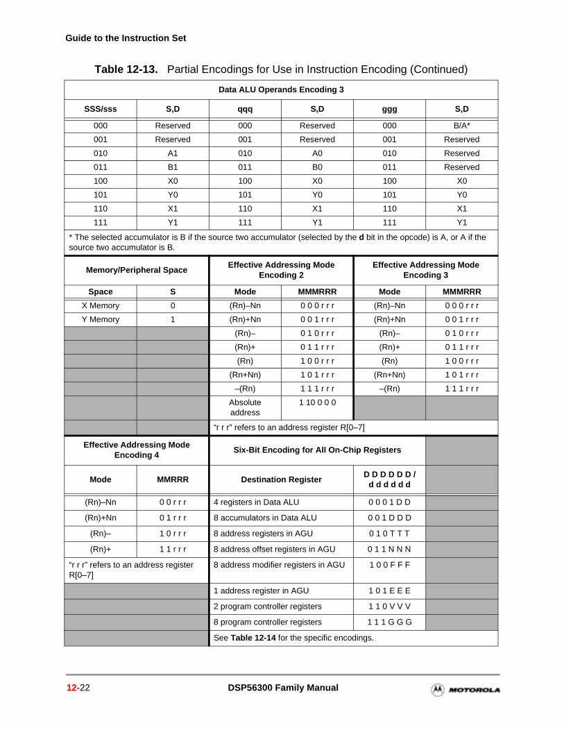
Guide to the Instruction Set
Data ALU Operands Encoding 3
SSS/sss S,D qqq S,D ggg S,D
000 Reserved 000 Reserved 000 B/A*
001 Reserved 001 Reserved 001 Reserved
010 A1 010 A0 010 Reserved
011 B1 011 B0 011 Reserved
100 X0 100 X0 100 X0
101 Y0 101 Y0 101 Y0
110 X1 110 X1 110 X1
111 Y1 111 Y1 111 Y1
* The selected accumulator is B if the source two accumulator (selected by the d bit in the opcode) is A, or A if the source two accumulator is B.
Memory/Peripheral SpaceEffective Addressing Mode
Encoding 2Effective Addressing Mode
Encoding 3
Space S Mode MMMRRR Mode MMMRRR
X Memory 0 (Rn)–Nn 0 0 0 r r r (Rn)–Nn 0 0 0 r r r
Y Memory 1 (Rn)+Nn 0 0 1 r r r (Rn)+Nn 0 0 1 r r r
(Rn)– 0 1 0 r r r (Rn)– 0 1 0 r r r
(Rn)+ 0 1 1 r r r (Rn)+ 0 1 1 r r r
(Rn) 1 0 0 r r r (Rn) 1 0 0 r r r
(Rn+Nn) 1 0 1 r r r (Rn+Nn) 1 0 1 r r r
–(Rn) 1 1 1 r r r –(Rn) 1 1 1 r r r
Absolute address
1 10 0 0 0
“r r r” refers to an address register R[0–7]
Effective Addressing Mode Encoding 4
Six-Bit Encoding for All On-Chip Registers
Mode MMRRR Destination RegisterD D D D D D /
d d d d d d
(Rn)–Nn 0 0 r r r 4 registers in Data ALU 0 0 0 1 D D
(Rn)+Nn 0 1 r r r 8 accumulators in Data ALU 0 0 1 D D D
(Rn)– 1 0 r r r 8 address registers in AGU 0 1 0 T T T
(Rn)+ 1 1 r r r 8 address offset registers in AGU 0 1 1 N N N
“r r r” refers to an address register R[0–7]
8 address modifier registers in AGU 1 0 0 F F F
1 address register in AGU 1 0 1 E E E
2 program controller registers 1 1 0 V V V
8 program controller registers 1 1 1 G G G
See Table 12-14 for the specific encodings.
Table 12-13. Partial Encodings for Use in Instruction Encoding (Continued)
12-22 DSP56300 Family Manual
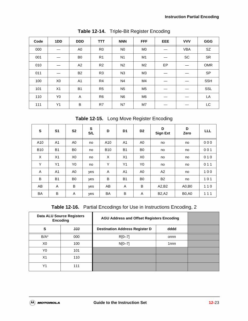
Instruction Partial Encoding
Table 12-14. Triple-Bit Register Encoding
Code 1DD DDD TTT NNN FFF EEE VVV GGG
000 — A0 R0 N0 M0 — VBA SZ
001 — B0 R1 N1 M1 — SC SR
010 — A2 R2 N2 M2 EP — OMR
011 — B2 R3 N3 M3 — — SP
100 X0 A1 R4 N4 M4 — — SSH
101 X1 B1 R5 N5 M5 — — SSL
110 Y0 A R6 N6 M6 — — LA
111 Y1 B R7 N7 M7 — — LC
Table 12-15. Long Move Register Encoding
S S1 S2S
S/LD D1 D2
DSign Ext
DZero
LLL
A10 A1 A0 no A10 A1 A0 no no 0 0 0
B10 B1 B0 no B10 B1 B0 no no 0 0 1
X X1 X0 no X X1 X0 no no 0 1 0
Y Y1 Y0 no Y Y1 Y0 no no 0 1 1
A A1 A0 yes A A1 A0 A2 no 1 0 0
B B1 B0 yes B B1 B0 B2 no 1 0 1
AB A B yes AB A B A2,B2 A0,B0 1 1 0
BA B A yes BA B A B2,A2 B0,A0 1 1 1
Table 12-16. Partial Encodings for Use in Instructions Encoding, 2
Data ALU Source Registers Encoding
AGU Address and Offset Registers Encoding
S JJJ Destination Address Register D dddd
B/A* 000 R[0–7] onnn
X0 100 N[0–7] 1nnn
Y0 101
X1 110
Y1 111
Guide to the Instruction Set 12-23
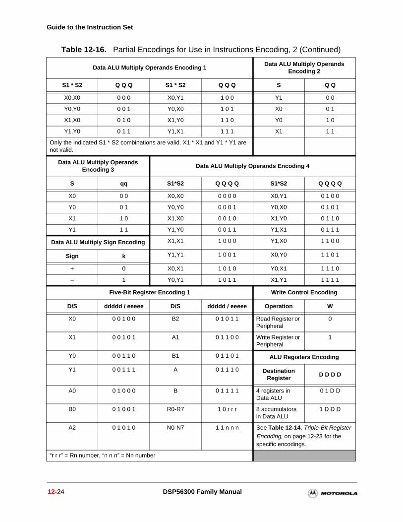
Guide to the Instruction Set
Data ALU Multiply Operands Encoding 1Data ALU Multiply Operands
Encoding 2
S1 * S2 Q Q Q S1 * S2 Q Q Q S Q Q
X0,X0 0 0 0 X0,Y1 1 0 0 Y1 0 0
Y0,Y0 0 0 1 Y0,X0 1 0 1 X0 0 1
X1,X0 0 1 0 X1,Y0 1 1 0 Y0 1 0
Y1,Y0 0 1 1 Y1,X1 1 1 1 X1 1 1
Only the indicated S1 * S2 combinations are valid. X1 * X1 and Y1 * Y1 are not valid.
Data ALU Multiply Operands Encoding 3
Data ALU Multiply Operands Encoding 4
S qq S1*S2 Q Q Q Q S1*S2 Q Q Q Q
X0 0 0 X0,X0 0 0 0 0 X0,Y1 0 1 0 0
Y0 0 1 Y0,Y0 0 0 0 1 Y0,X0 0 1 0 1
X1 1 0 X1,X0 0 0 1 0 X1,Y0 0 1 1 0
Y1 1 1 Y1,Y0 0 0 1 1 Y1,X1 0 1 1 1
Data ALU Multiply Sign Encoding X1,X1 1 0 0 0 Y1,X0 1 1 0 0
Sign k Y1,Y1 1 0 0 1 X0,Y0 1 1 0 1
+ 0 X0,X1 1 0 1 0 Y0,X1 1 1 1 0
– 1 Y0,Y1 1 0 1 1 X1,Y1 1 1 1 1
Five-Bit Register Encoding 1 Write Control Encoding
D/S ddddd / eeeee D/S ddddd / eeeee Operation W
X0 0 0 1 0 0 B2 0 1 0 1 1 Read Register or Peripheral
0
X1 0 0 1 0 1 A1 0 1 1 0 0 Write Register or Peripheral
1
Y0 0 0 1 1 0 B1 0 1 1 0 1 ALU Registers Encoding
Y1 0 0 1 1 1 A 0 1 1 1 0 Destination Register
D D D D
A0 0 1 0 0 0 B 0 1 1 1 1 4 registers in Data ALU
0 1 D D
B0 0 1 0 0 1 R0-R7 1 0 r r r 8 accumulators in Data ALU
1 D D D
A2 0 1 0 1 0 N0-N7 1 1 n n n See Table 12-14, Triple-Bit Register Encoding, on page 12-23 for the specific encodings.
“r r r” = Rn number, “n n n” = Nn number
Table 12-16. Partial Encodings for Use in Instructions Encoding, 2 (Continued)
12-24 DSP56300 Family Manual
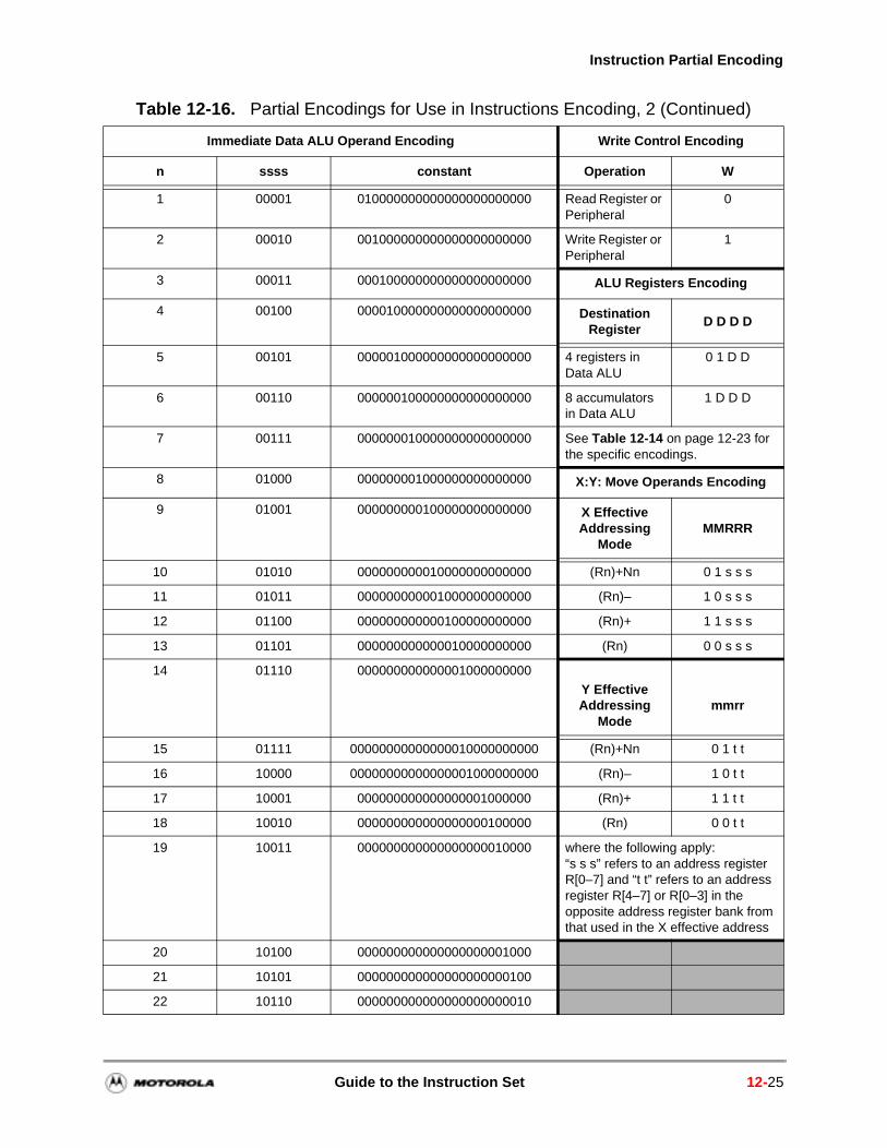
Instruction Partial Encoding
Immediate Data ALU Operand Encoding Write Control Encoding
n ssss constant Operation W
1 00001 010000000000000000000000 Read Register or Peripheral
0
2 00010 001000000000000000000000 Write Register or Peripheral
1
3 00011 000100000000000000000000 ALU Registers Encoding
4 00100 000010000000000000000000 Destination Register
D D D D
5 00101 000001000000000000000000 4 registers in Data ALU
0 1 D D
6 00110 000000100000000000000000 8 accumulators in Data ALU
1 D D D
7 00111 000000010000000000000000 See Table 12-14 on page 12-23 for the specific encodings.
8 01000 000000001000000000000000 X:Y: Move Operands Encoding
9 01001 000000000100000000000000 X Effective Addressing
ModeMMRRR
10 01010 000000000010000000000000 (Rn)+Nn 0 1 s s s
11 01011 000000000001000000000000 (Rn)– 1 0 s s s
12 01100 000000000000100000000000 (Rn)+ 1 1 s s s
13 01101 000000000000010000000000 (Rn) 0 0 s s s
14 01110 000000000000001000000000
Y Effective Addressing
Modemmrr
15 01111 00000000000000010000000000 (Rn)+Nn 0 1 t t
16 10000 00000000000000001000000000 (Rn)– 1 0 t t
17 10001 000000000000000001000000 (Rn)+ 1 1 t t
18 10010 000000000000000000100000 (Rn) 0 0 t t
19 10011 000000000000000000010000 where the following apply: “s s s” refers to an address register R[0–7] and “t t” refers to an address register R[4–7] or R[0–3] in the opposite address register bank from that used in the X effective address
20 10100 000000000000000000001000
21 10101 000000000000000000000100
22 10110 000000000000000000000010
Table 12-16. Partial Encodings for Use in Instructions Encoding, 2 (Continued)
Guide to the Instruction Set 12-25
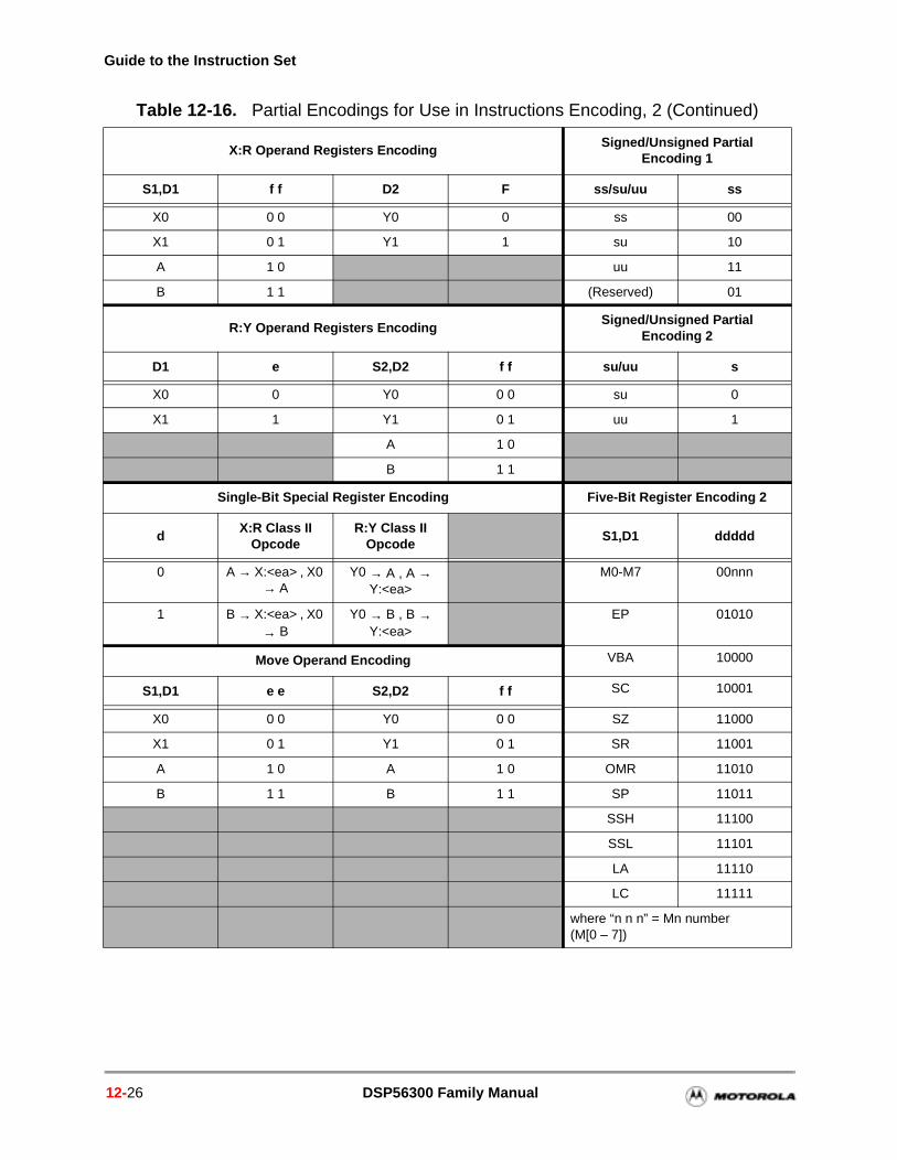
Guide to the Instruction Set
X:R Operand Registers EncodingSigned/Unsigned Partial
Encoding 1
S1,D1 f f D2 F ss/su/uu ss
X0 0 0 Y0 0 ss 00
X1 0 1 Y1 1 su 10
A 1 0 uu 11
B 1 1 (Reserved) 01
R:Y Operand Registers EncodingSigned/Unsigned Partial
Encoding 2
D1 e S2,D2 f f su/uu s
X0 0 Y0 0 0 su 0
X1 1 Y1 0 1 uu 1
A 1 0
B 1 1
Single-Bit Special Register Encoding Five-Bit Register Encoding 2
dX:R Class II
OpcodeR:Y Class II
OpcodeS1,D1 ddddd
0 A → X:<ea> , X0 → A
Y0 → A , A → Y:<ea>
M0-M7 00nnn
1 B → X:<ea> , X0 → B
Y0 → B , B → Y:<ea>
EP 01010
Move Operand Encoding VBA 10000
S1,D1 e e S2,D2 f f SC 10001
X0 0 0 Y0 0 0 SZ 11000
X1 0 1 Y1 0 1 SR 11001
A 1 0 A 1 0 OMR 11010
B 1 1 B 1 1 SP 11011
SSH 11100
SSL 11101
LA 11110
LC 11111
where “n n n” = Mn number (M[0 – 7])
Table 12-16. Partial Encodings for Use in Instructions Encoding, 2 (Continued)
12-26 DSP56300 Family Manual
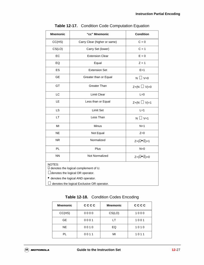
Instruction Partial Encoding
Table 12-17. Condition Code Computation Equation
Mnemonic “cc” Mnemonic Condition
CC(HS) Carry Clear (higher or same) C = 0
CS(LO) Carry Set (lower) C = 1
EC Extension Clear E = 0
EQ Equal Z = 1
ES Extension Set E=1
GE Greater than or Equal N ⊕ V=0
GT Greater Than Z+(N ⊕ V)=0
LC Limit Clear L=0
LE Less than or Equal Z+(N ⊕ V)=1
LS Limit Set L=1
LT Less Than N ⊕ V=1
MI Minus N=1
NE Not Equal Z=0
NR Normalized Z+(U•E)=1
PL Plus N=0
NN Not Normalized Z+(U•E)=0
NOTES:U denotes the logical complement of U.
+ denotes the logical OR operator.
• denotes the logical AND operator.
⊕ denotes the logical Exclusive OR operator.
Table 12-18. Condition Codes Encoding
Mnemonic C C C C Mnemonic C C C C
CC(HS) 0 0 0 0 CS(LO) 1 0 0 0
GE 0 0 0 1 LT 1 0 0 1
NE 0 0 1 0 EQ 1 0 1 0
PL 0 0 1 1 MI 1 0 1 1
Guide to the Instruction Set 12-27
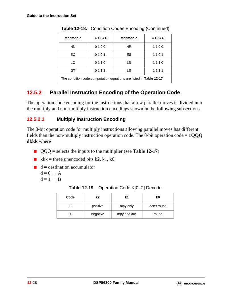
Guide to the Instruction Set
12.5.2 Parallel Instruction Encoding of the Operation Code
The operation code encoding for the instructions that allow parallel moves is divided into the multiply and non-multiply instruction encodings shown in the following subsections.
12.5.2.1 Multiply Instruction Encoding
The 8-bit operation code for multiply instructions allowing parallel moves has different fields than the non-multiply instruction operation code. The 8-bit operation code = 1QQQ dkkk where
QQQ = selects the inputs to the multiplier (see Table 12-17)
kkk = three unencoded bits k2, k1, k0
d = destination accumulatord = 0 → Ad = 1 → B
NN 0 1 0 0 NR 1 1 0 0
EC 0 1 0 1 ES 1 1 0 1
LC 0 1 1 0 LS 1 1 1 0
GT 0 1 1 1 LE 1 1 1 1
The condition code computation equations are listed in Table 12-17.
Table 12-19. Operation Code K[0–2] Decode
Code k2 k1 k0
0 positive mpy only don’t round
1 negative mpy and acc round
Table 12-18. Condition Codes Encoding (Continued)
Mnemonic C C C C Mnemonic C C C C
12-28 DSP56300 Family Manual
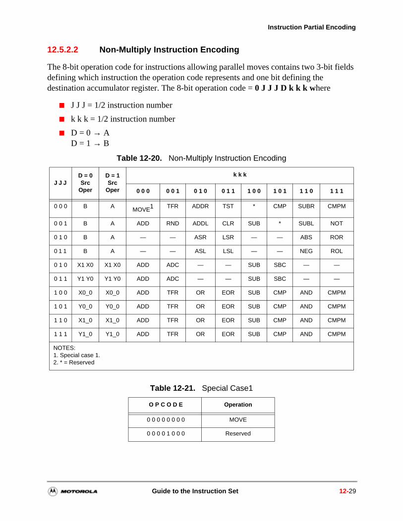
Instruction Partial Encoding
12.5.2.2 Non-Multiply Instruction Encoding
The 8-bit operation code for instructions allowing parallel moves contains two 3-bit fields defining which instruction the operation code represents and one bit defining the destination accumulator register. The 8-bit operation code = 0 J J J D k k k where
J J J = 1/2 instruction number
k k k = 1/2 instruction number
D = 0 → AD = 1 → B
Table 12-20. Non-Multiply Instruction Encoding
J J J D = 0Src
Oper
D = 1Src
Oper
k k k
0 0 0 0 0 1 0 1 0 0 1 1 1 0 0 1 0 1 1 1 0 1 1 1
0 0 0 B A MOVE1 TFR ADDR TST * CMP SUBR CMPM
0 0 1 B A ADD RND ADDL CLR SUB * SUBL NOT
0 1 0 B A — — ASR LSR — — ABS ROR
0 1 1 B A — — ASL LSL — — NEG ROL
0 1 0 X1 X0 X1 X0 ADD ADC — — SUB SBC — —
0 1 1 Y1 Y0 Y1 Y0 ADD ADC — — SUB SBC — —
1 0 0 X0_0 X0_0 ADD TFR OR EOR SUB CMP AND CMPM
1 0 1 Y0_0 Y0_0 ADD TFR OR EOR SUB CMP AND CMPM
1 1 0 X1_0 X1_0 ADD TFR OR EOR SUB CMP AND CMPM
1 1 1 Y1_0 Y1_0 ADD TFR OR EOR SUB CMP AND CMPM
NOTES:1. Special case 1.2. * = Reserved
Table 12-21. Special Case1
O P C O D E Operation
0 0 0 0 0 0 0 0 MOVE
0 0 0 0 1 0 0 0 Reserved
Guide to the Instruction Set 12-29

Guide to the Instruction Set
12-30 DSP56300 Family Manual
Chapter 13Instruction SetThis chapter describes each instruction in the DSP56300 (family) core instruction set in detail. Instructions that allow parallel moves are so noted in both the Operation and the Assembler Syntax fields. The MOVE instruction is equivalent to a NOP with parallel moves, so a description of each parallel move accompanies the MOVE instruction details. When an instruction uses an accumulator as both a destination operand for Data ALU operation and a source for a parallel move operation, the parallel move operation uses the value in the accumulator before any Data ALU operation executes. Use Table 13-1 to locate the page number of an instruction. Refer to Chapter 12, Guide to the Instruction Set, for details on instruction formats, syntax, descriptions, groups, operand lengths, and encoding.
Table 13-1. DSP56300 Instruction Summary
Instruction Page Instruction Page
ABSAbsolute Value
page 13-5 BRABranch Always
page 13-25
ADCAdd Long With Carry
page 13-6 BRCLRBranch if Bit Clear
page 13-26
ADDAdd
page 13-7 BRKccExit Current DO Loop Conditionally
page 13-28
ADDLShift Left and Add Accumulators
page 13-9 BRSETBranch if Bit Set
page 13-29
ADDRShift Right and Add Accumulators
page 13-10 BSccBranch to Subroutine Conditionally
page 13-31
ANDLogical AND
page 13-11 BSCLRBranch to Subroutine if Bit Clear
page 13-33
ANDIAND Immediate With Control Register
page 13-13 BSETBit Set and Test
page 13-35
ASLArithmetic Shift Accumulator Left
page 13-14 BSRBranch to Subroutine
page 13-38
ASRArithmetic Shift Accumulator Right
page 13-16 BSSETBranch to Subroutine if Bit Set
page 13-39
BccBranch Conditionally
page 13-18 BTSTBit Test
page 13-41
DSP56300 Family Manual 13-1
BCHGBit Test and Change
page 13-19 CLBCount Leading Bits
page 13-43
BCLRBit Test and Clear
page 13-22 CLRClear Accumulator
page 13-45
CMPCompare
page 13-46 INCIncrement by One
page 13-77
CMPMCompare Magnitude
page 13-48 INSERTInsert Bit Field
page 13-78
CMPUCompare Unsigned
page 13-49 JccJump Conditionally
page 13-80
DEBUGEnter Debug Mode
page 13-50 JCLRJump if Bit Clear
page 13-81
DEBUGccEnter Debug Mode Conditionally
page 13-51 JMPJump
page 13-83
DECDecrement by One
page 13-52 JSccJump to Subroutine Conditionally
page 13-84
DIVDivide Iteration
page 13-52 JSCLRJump to Subroutine if Bit Clear
page 13-85
DMACDouble-Precision Multiply-Accumulate With Right Shift
page 13-56 JSETJump if Bit Set
page 13-87
DOStart Hardware Loop
page 13-57 JSRJump to Subroutine
page 13-89
DO FOREVERStart Infinite Loop
page 13-60 JSSETJump to Subroutine if Bit Set
page 13-90
DORStart PC-Relative Hardware Loop
page 13-62 L:Long Memory Data Move
page 13-126
DOR FOREVERStart PC-Relative Infinite Loop
page 13-65 LRALoad PC-Relative Address
page 13-92
ENDDOEnd Current DO Loop
page 13-67 LSLLogical Shift Left
page 13-93
EORLogical Exclusive OR
page 13-68 LSRLogical Shift Right
page 13-96
EXTRACTExtract Bit Field
page 13-70 LUALoad Updated Address
page 13-98
EXTRACTUExtract Unsigned Bit Field
page 13-72 MACSigned Multiply Accumulate
page 13-99
IImmediate Short Data Move
page 13-113 MAC(su,uu)Mixed Multiply Accumulate
page 13-102
IFccExecute Conditionally Without CCR Update
page 13-74 MACISigned Multiply Accumulate With Immediate Operand
page 13-101
IFcc.UExecute Conditionally With CCR Update
page 13-75 MACRSigned Multiply Accumulate and Round
page 13-103
Table 13-1. DSP56300 Instruction Summary (Continued)
Instruction Page Instruction Page
13-2 DSP56300 Family Manual
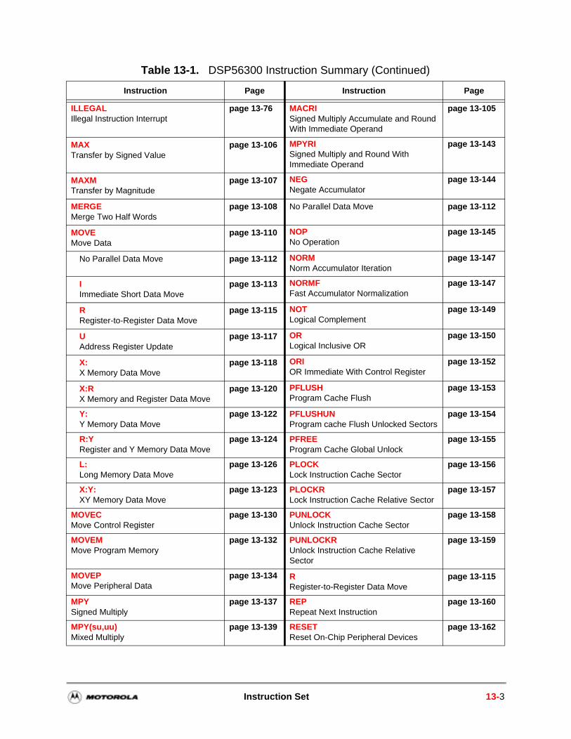
ILLEGALIllegal Instruction Interrupt
page 13-76 MACRISigned Multiply Accumulate and Round With Immediate Operand
page 13-105
MAXTransfer by Signed Value
page 13-106 MPYRISigned Multiply and Round With Immediate Operand
page 13-143
MAXMTransfer by Magnitude
page 13-107 NEGNegate Accumulator
page 13-144
MERGEMerge Two Half Words
page 13-108 No Parallel Data Move page 13-112
MOVEMove Data
page 13-110 NOPNo Operation
page 13-145
No Parallel Data Move page 13-112 NORMNorm Accumulator Iteration
page 13-147
IImmediate Short Data Move
page 13-113 NORMFFast Accumulator Normalization
page 13-147
RRegister-to-Register Data Move
page 13-115 NOTLogical Complement
page 13-149
UAddress Register Update
page 13-117 ORLogical Inclusive OR
page 13-150
X:X Memory Data Move
page 13-118 ORIOR Immediate With Control Register
page 13-152
X:RX Memory and Register Data Move
page 13-120 PFLUSHProgram Cache Flush
page 13-153
Y:Y Memory Data Move
page 13-122 PFLUSHUNProgram cache Flush Unlocked Sectors
page 13-154
R:YRegister and Y Memory Data Move
page 13-124 PFREEProgram Cache Global Unlock
page 13-155
L:Long Memory Data Move
page 13-126 PLOCKLock Instruction Cache Sector
page 13-156
X:Y:XY Memory Data Move
page 13-123 PLOCKRLock Instruction Cache Relative Sector
page 13-157
MOVECMove Control Register
page 13-130 PUNLOCKUnlock Instruction Cache Sector
page 13-158
MOVEMMove Program Memory
page 13-132 PUNLOCKRUnlock Instruction Cache Relative Sector
page 13-159
MOVEPMove Peripheral Data
page 13-134 RRegister-to-Register Data Move
page 13-115
MPYSigned Multiply
page 13-137 REPRepeat Next Instruction
page 13-160
MPY(su,uu)Mixed Multiply
page 13-139 RESETReset On-Chip Peripheral Devices
page 13-162
Table 13-1. DSP56300 Instruction Summary (Continued)
Instruction Page Instruction Page
Instruction Set 13-3
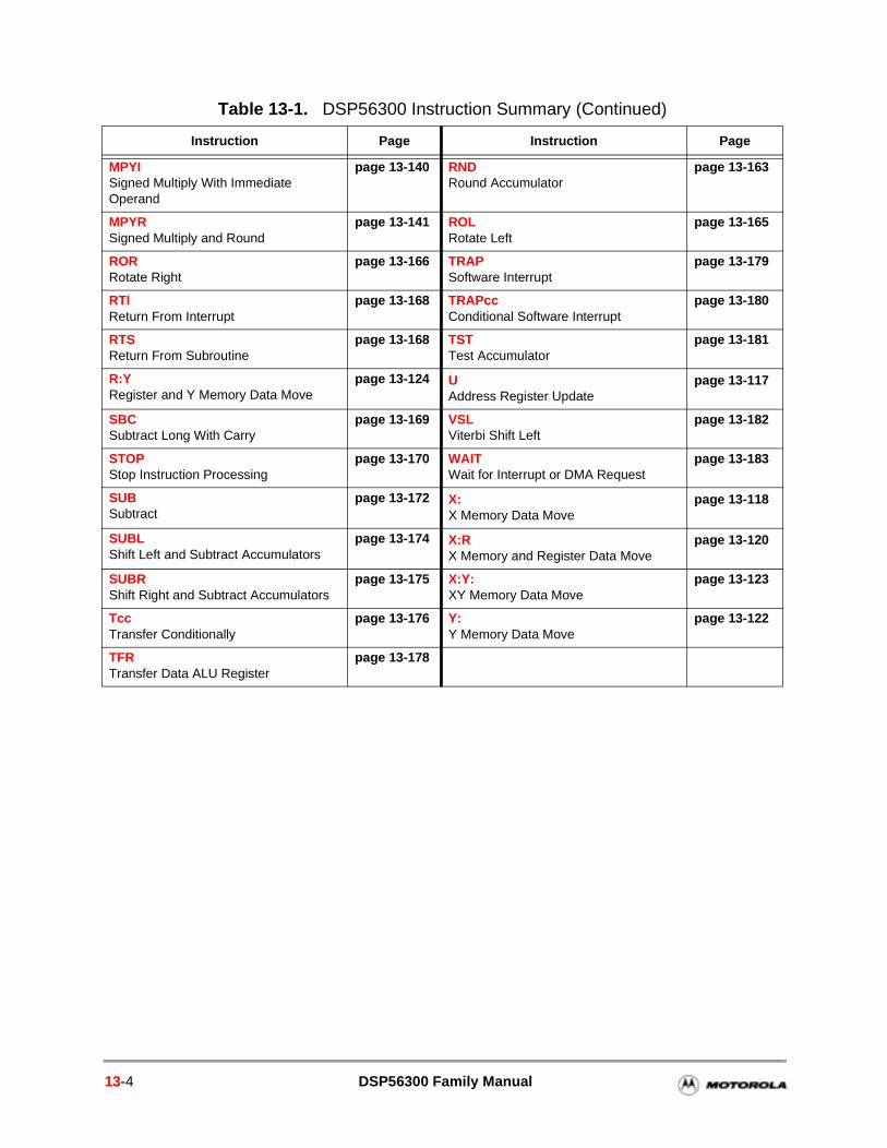
MPYISigned Multiply With Immediate Operand
page 13-140 RNDRound Accumulator
page 13-163
MPYRSigned Multiply and Round
page 13-141 ROLRotate Left
page 13-165
RORRotate Right
page 13-166 TRAPSoftware Interrupt
page 13-179
RTIReturn From Interrupt
page 13-168 TRAPccConditional Software Interrupt
page 13-180
RTSReturn From Subroutine
page 13-168 TSTTest Accumulator
page 13-181
R:YRegister and Y Memory Data Move
page 13-124 UAddress Register Update
page 13-117
SBCSubtract Long With Carry
page 13-169 VSLViterbi Shift Left
page 13-182
STOPStop Instruction Processing
page 13-170 WAITWait for Interrupt or DMA Request
page 13-183
SUBSubtract
page 13-172 X:X Memory Data Move
page 13-118
SUBLShift Left and Subtract Accumulators
page 13-174 X:RX Memory and Register Data Move
page 13-120
SUBRShift Right and Subtract Accumulators
page 13-175 X:Y:XY Memory Data Move
page 13-123
TccTransfer Conditionally
page 13-176 Y:Y Memory Data Move
page 13-122
TFRTransfer Data ALU Register
page 13-178
Table 13-1. DSP56300 Instruction Summary (Continued)
Instruction Page Instruction Page
13-4 DSP56300 Family Manual
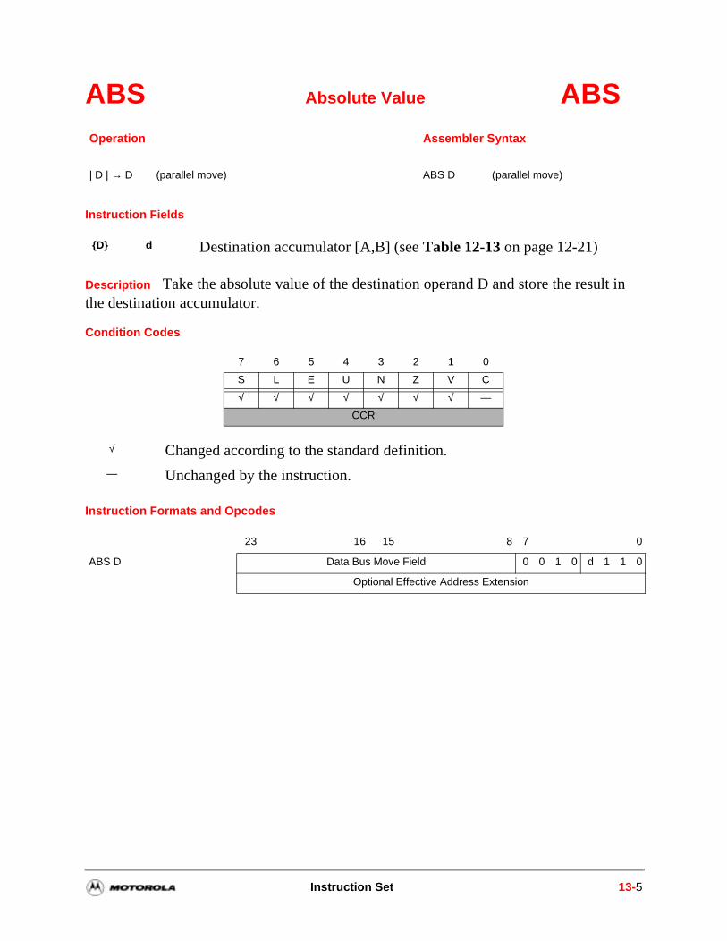
ABS Absolute Value ABS
Instruction Fields
Description Take the absolute value of the destination operand D and store the result in the destination accumulator.
Condition Codes
Instruction Formats and Opcodes
Operation Assembler Syntax
| D | → D (parallel move) ABS D (parallel move)
D d Destination accumulator [A,B] (see Table 12-13 on page 12-21)
7 6 5 4 3 2 1 0
S L E U N Z V C
√ √ √ √ √ √ √ —
CCR
√ Changed according to the standard definition.
— Unchanged by the instruction.
23 16 15 8 7 0
ABS D Data Bus Move Field 0 0 1 0 d 1 1 0
Optional Effective Address Extension
Instruction Set 13-5
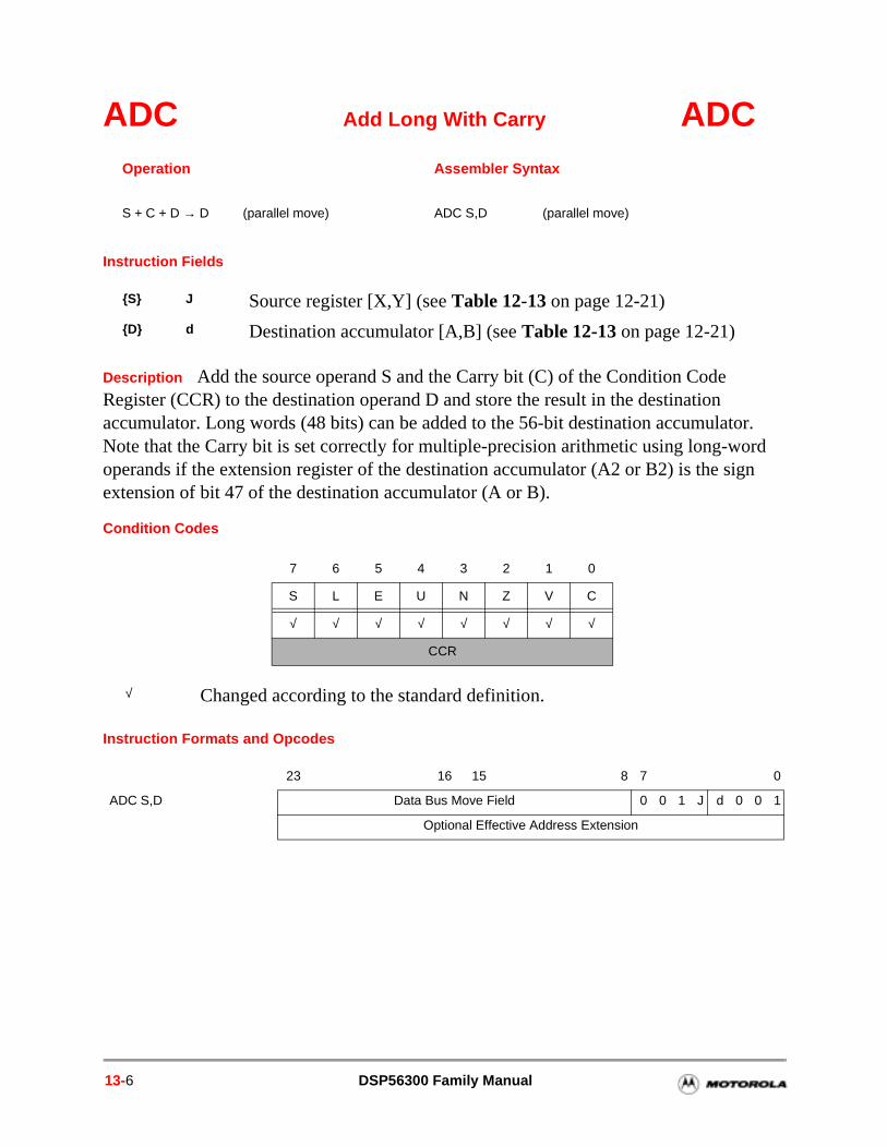
ADC Add Long With Carry ADC
Instruction Fields
Description Add the source operand S and the Carry bit (C) of the Condition Code Register (CCR) to the destination operand D and store the result in the destination accumulator. Long words (48 bits) can be added to the 56-bit destination accumulator. Note that the Carry bit is set correctly for multiple-precision arithmetic using long-word operands if the extension register of the destination accumulator (A2 or B2) is the sign extension of bit 47 of the destination accumulator (A or B).
Condition Codes
Instruction Formats and Opcodes
Operation Assembler Syntax
S + C + D → D (parallel move) ADC S,D (parallel move)
S J Source register [X,Y] (see Table 12-13 on page 12-21)
D d Destination accumulator [A,B] (see Table 12-13 on page 12-21)
7 6 5 4 3 2 1 0
S L E U N Z V C
√ √ √ √ √ √ √ √
CCR
√ Changed according to the standard definition.
23 16 15 8 7 0
ADC S,D Data Bus Move Field 0 0 1 J d 0 0 1
Optional Effective Address Extension
13-6 DSP56300 Family Manual
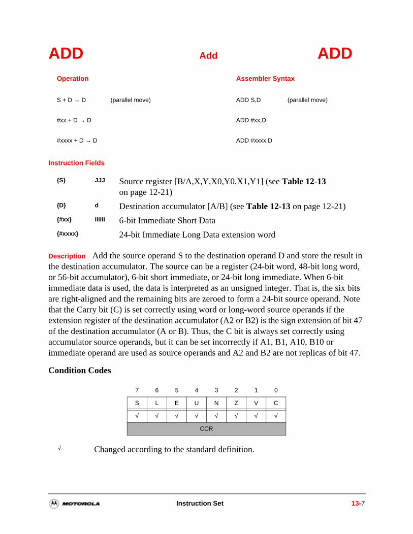
ADD Add ADD
Instruction Fields
Description Add the source operand S to the destination operand D and store the result in the destination accumulator. The source can be a register (24-bit word, 48-bit long word, or 56-bit accumulator), 6-bit short immediate, or 24-bit long immediate. When 6-bit immediate data is used, the data is interpreted as an unsigned integer. That is, the six bits are right-aligned and the remaining bits are zeroed to form a 24-bit source operand. Note that the Carry bit (C) is set correctly using word or long-word source operands if the extension register of the destination accumulator (A2 or B2) is the sign extension of bit 47 of the destination accumulator (A or B). Thus, the C bit is always set correctly using accumulator source operands, but it can be set incorrectly if A1, B1, A10, B10 or immediate operand are used as source operands and A2 and B2 are not replicas of bit 47.
Condition Codes
Operation Assembler Syntax
S + D → D (parallel move) ADD S,D (parallel move)
#xx + D → D ADD #xx,D
#xxxx + D → D ADD #xxxx,D
S JJJ Source register [B/A,X,Y,X0,Y0,X1,Y1] (see Table 12-13 on page 12-21)
D d Destination accumulator [A/B] (see Table 12-13 on page 12-21)
#xx iiiiii 6-bit Immediate Short Data
#xxxx 24-bit Immediate Long Data extension word
7 6 5 4 3 2 1 0
S L E U N Z V C
√ √ √ √ √ √ √ √
CCR
√ Changed according to the standard definition.
Instruction Set 13-7
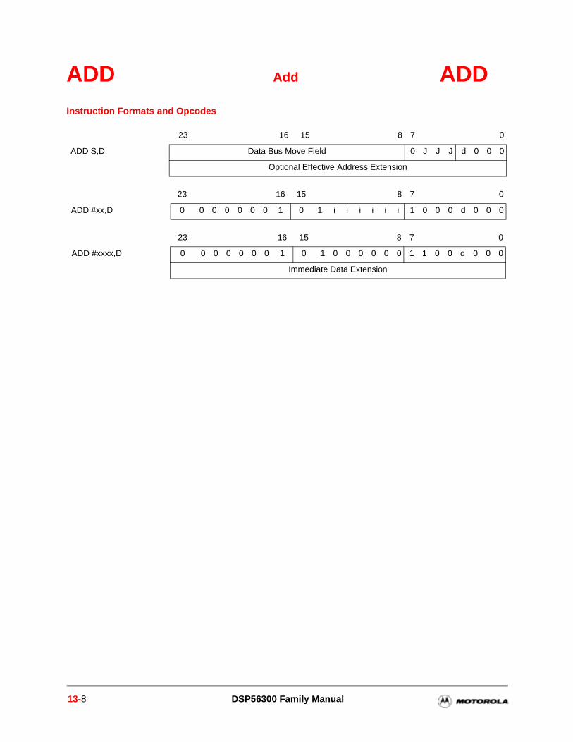
ADD Add ADDInstruction Formats and Opcodes
23 16 15 8 7 0
ADD S,D Data Bus Move Field 0 J J J d 0 0 0
Optional Effective Address Extension
23 16 15 8 7 0
ADD #xx,D 0 0 0 0 0 0 0 1 0 1 i i i i i i 1 0 0 0 d 0 0 0
23 16 15 8 7 0
ADD #xxxx,D 0 0 0 0 0 0 0 1 0 1 0 0 0 0 0 0 1 1 0 0 d 0 0 0
Immediate Data Extension
13-8 DSP56300 Family Manual
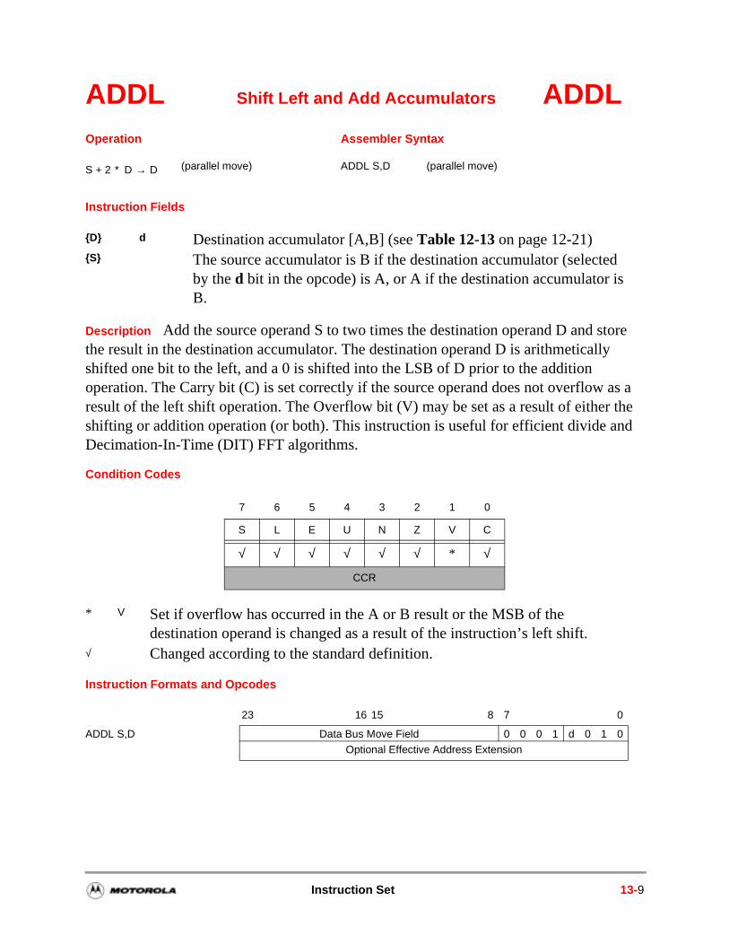
ADDL Shift Left and Add Accumulators ADDL
Instruction Fields
Description Add the source operand S to two times the destination operand D and store the result in the destination accumulator. The destination operand D is arithmetically shifted one bit to the left, and a 0 is shifted into the LSB of D prior to the addition operation. The Carry bit (C) is set correctly if the source operand does not overflow as a result of the left shift operation. The Overflow bit (V) may be set as a result of either the shifting or addition operation (or both). This instruction is useful for efficient divide and Decimation-In-Time (DIT) FFT algorithms.
Condition Codes
Instruction Formats and Opcodes
Operation Assembler Syntax
S + 2 ∗ D → D (parallel move) ADDL S,D (parallel move)
D d Destination accumulator [A,B] (see Table 12-13 on page 12-21)S The source accumulator is B if the destination accumulator (selected
by the d bit in the opcode) is A, or A if the destination accumulator is B.
7 6 5 4 3 2 1 0
S L E U N Z V C
√ √ √ √ √ √ * √
CCR
* V Set if overflow has occurred in the A or B result or the MSB of the destination operand is changed as a result of the instruction’s left shift.
√ Changed according to the standard definition.
23 16 15 8 7 0
ADDL S,D Data Bus Move Field 0 0 0 1 d 0 1 0
Optional Effective Address Extension
Instruction Set 13-9
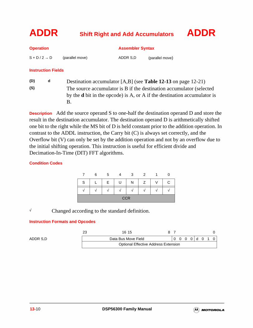
ADDR Shift Right and Add Accumulators ADDR
Instruction Fields
Description Add the source operand S to one-half the destination operand D and store the result in the destination accumulator. The destination operand D is arithmetically shifted one bit to the right while the MS bit of D is held constant prior to the addition operation. In contrast to the ADDL instruction, the Carry bit (C) is always set correctly, and the Overflow bit (V) can only be set by the addition operation and not by an overflow due to the initial shifting operation. This instruction is useful for efficient divide and Decimation-In-Time (DIT) FFT algorithms.
Condition Codes
Instruction Formats and Opcodes
Operation Assembler Syntax
S + D / 2 → D (parallel move) ADDR S,D (parallel move)
D d Destination accumulator [A,B] (see Table 12-13 on page 12-21)S The source accumulator is B if the destination accumulator (selected
by the d bit in the opcode) is A, or A if the destination accumulator is B.
7 6 5 4 3 2 1 0
S L E U N Z V C
√ √ √ √ √ √ √ √
CCR
√ Changed according to the standard definition.
23 16 15 8 7 0
ADDR S,D Data Bus Move Field 0 0 0 0 d 0 1 0
Optional Effective Address Extension
13-10 DSP56300 Family Manual
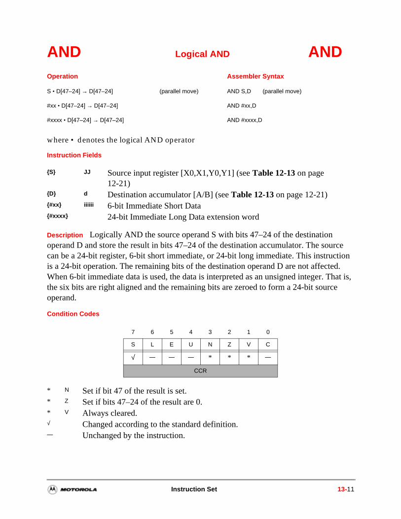
rce tion d. hat is, e
AND Logical AND AND
where • denotes the logical AND operator
Instruction Fields
Description Logically AND the source operand S with bits 47–24 of the destination operand D and store the result in bits 47–24 of the destination accumulator. The soucan be a 24-bit register, 6-bit short immediate, or 24-bit long immediate. This instrucis a 24-bit operation. The remaining bits of the destination operand D are not affecteWhen 6-bit immediate data is used, the data is interpreted as an unsigned integer. Tthe six bits are right aligned and the remaining bits are zeroed to form a 24-bit sourcoperand.
Condition Codes
Operation Assembler Syntax
S • D[47–24] → D[47–24] (parallel move) AND S,D (parallel move)
#xx • D[47–24] → D[47–24] AND #xx,D
#xxxx • D[47–24] → D[47–24] AND #xxxx,D
S JJ Source input register [X0,X1,Y0,Y1] (see Table 12-13 on page 12-21)
D d Destination accumulator [A/B] (see Table 12-13 on page 12-21)#xx iiiiii 6-bit Immediate Short Data #xxxx 24-bit Immediate Long Data extension word
7 6 5 4 3 2 1 0
S L E U N Z V C
√ — — — * * * —
CCR
* N Set if bit 47 of the result is set.* Z Set if bits 47–24 of the result are 0. * V Always cleared.√ Changed according to the standard definition.— Unchanged by the instruction.
Instruction Set 13-11
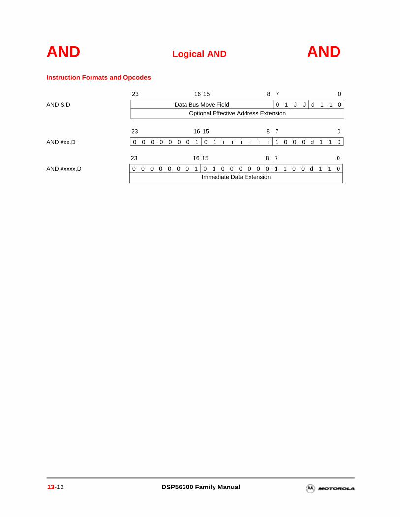
AND Logical AND ANDInstruction Formats and Opcodes
23 16 15 8 7 0
AND S,D Data Bus Move Field 0 1 J J d 1 1 0Optional Effective Address Extension
23 16 15 8 7 0
AND #xx,D 0 0 0 0 0 0 0 1 0 1 i i i i i i 1 0 0 0 d 1 1 0
23 16 15 8 7 0
AND #xxxx,D 0 0 0 0 0 0 0 1 0 1 0 0 0 0 0 0 1 1 0 0 d 1 1 0
Immediate Data Extension
13-12 DSP56300 Family Manual
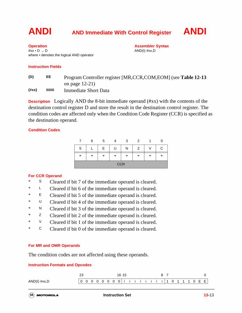
ANDI AND Immediate With Control Register ANDI
Instruction Fields
Description Logically AND the 8-bit immediate operand (#xx) with the contents of the destination control register D and store the result in the destination control register. The condition codes are affected only when the Condition Code Register (CCR) is specified as the destination operand.
Condition Codes
Instruction Formats and Opcodes
Operation Assembler Syntax #xx • D → D AND(I) #xx,Dwhere • denotes the logical AND operator
D EE Program Controller register [MR,CCR,COM,EOM] (see Table 12-13 on page 12-21)
#xx iiiiiiii Immediate Short Data
7 6 5 4 3 2 1 0
S L E U N Z V C
* * * * * * * *
CCR
For CCR Operand* S Cleared if bit 7 of the immediate operand is cleared.* L Cleared if bit 6 of the immediate operand is cleared.* E Cleared if bit 5 of the immediate operand is cleared.* U Cleared if bit 4 of the immediate operand is cleared.* N Cleared if bit 3 of the immediate operand is cleared.* Z Cleared if bit 2 of the immediate operand is cleared.* V Cleared if bit 1 of the immediate operand is cleared.* C Cleared if bit 0 of the immediate operand is cleared.
For MR and OMR Operands
The condition codes are not affected using these operands.
23 16 15 8 7 0
AND(I) #xx,D 0 0 0 0 0 0 0 0 i i i i i i i i 1 0 1 1 1 0 E E
Instruction Set 13-13
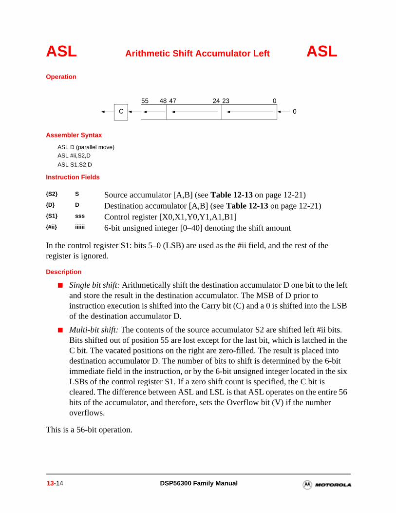
eft
SB
ts. the to bit six
re 56
ASL Arithmetic Shift Accumulator Left ASLOperation
Assembler Syntax
ASL D (parallel move)ASL #ii,S2,D
ASL S1,S2,D
Instruction Fields
In the control register S1: bits 5–0 (LSB) are used as the #ii field, and the rest of the register is ignored.
Description
Single bit shift: Arithmetically shift the destination accumulator D one bit to the land store the result in the destination accumulator. The MSB of D prior to instruction execution is shifted into the Carry bit (C) and a 0 is shifted into the Lof the destination accumulator D.
Multi-bit shift: The contents of the source accumulator S2 are shifted left #ii biBits shifted out of position 55 are lost except for the last bit, which is latched inC bit. The vacated positions on the right are zero-filled. The result is placed indestination accumulator D. The number of bits to shift is determined by the 6-immediate field in the instruction, or by the 6-bit unsigned integer located in theLSBs of the control register S1. If a zero shift count is specified, the C bit is cleared. The difference between ASL and LSL is that ASL operates on the entibits of the accumulator, and therefore, sets the Overflow bit (V) if the number overflows.
This is a 56-bit operation.
S2 S Source accumulator [A,B] (see Table 12-13 on page 12-21)D D Destination accumulator [A,B] (see Table 12-13 on page 12-21)S1 sss Control register [X0,X1,Y0,Y1,A1,B1] #ii iiiiii 6-bit unsigned integer [0–40] denoting the shift amount
C 0
55 47 23 048 24
13-14 DSP56300 Family Manual
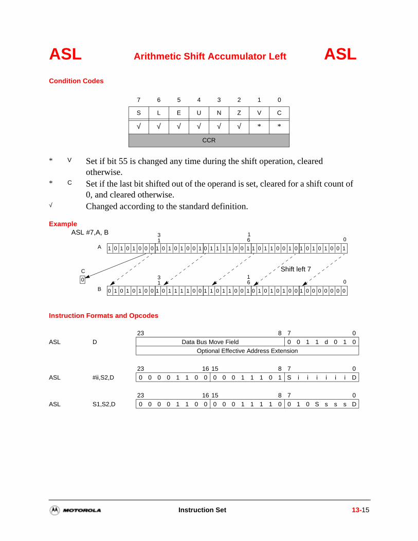
ASL Arithmetic Shift Accumulator Left ASLCondition Codes
Example
Instruction Formats and Opcodes
7 6 5 4 3 2 1 0
S L E U N Z V C
√ √ √ √ √ √ * *
CCR
* V Set if bit 55 is changed any time during the shift operation, cleared otherwise.
* C Set if the last bit shifted out of the operand is set, cleared for a shift count of 0, and cleared otherwise.
√ Changed according to the standard definition.
23 8 7 0ASL D Data Bus Move Field 0 0 1 1 d 0 1 0
Optional Effective Address Extension
23 16 15 8 7 0ASL #ii,S2,D 0 0 0 0 1 1 0 0 0 0 0 1 1 1 0 1 S i i i i i i D
23 16 15 8 7 0ASL S1,S2,D 0 0 0 0 1 1 0 0 0 0 0 1 1 1 1 0 0 1 0 S s s s D
631
1
Shift left 7
0
0
C
1 0 1 0 1 0 0 0A
B
1 0 1 0 1 0 0 1 0 1 1 1 1 0 0 1 1 0 1 1 0 0 1 0 1 0 1 0 1 0 0 1
631
10
0 1 0 1 0 1 0 0 1 0 1 1 1 1 0 0 1 1 0 1 1 0 0 1 0 1 0 1 0 1 0 0 1 0 0 0 0 0 0 0
ASL #7,A, B
Instruction Set 13-15
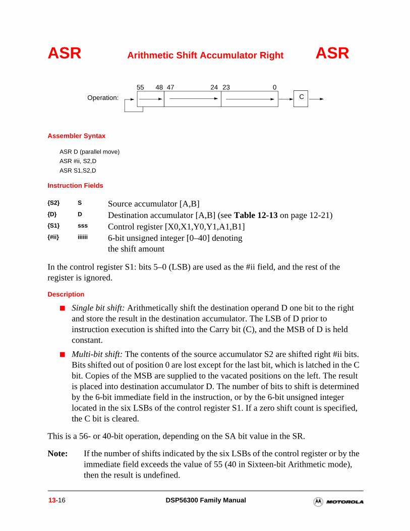
t
its. e C
esult ined
ied,
the ),
ASR Arithmetic Shift Accumulator Right ASR
Assembler Syntax
ASR D (parallel move)
ASR #ii, S2,D
ASR S1,S2,D
Instruction Fields
In the control register S1: bits 5–0 (LSB) are used as the #ii field, and the rest of the register is ignored.
Description
Single bit shift: Arithmetically shift the destination operand D one bit to the righand store the result in the destination accumulator. The LSB of D prior to instruction execution is shifted into the Carry bit (C), and the MSB of D is heldconstant.
Multi-bit shift: The contents of the source accumulator S2 are shifted right #ii bBits shifted out of position 0 are lost except for the last bit, which is latched in thbit. Copies of the MSB are supplied to the vacated positions on the left. The ris placed into destination accumulator D. The number of bits to shift is determby the 6-bit immediate field in the instruction, or by the 6-bit unsigned integer located in the six LSBs of the control register S1. If a zero shift count is specifthe C bit is cleared.
This is a 56- or 40-bit operation, depending on the SA bit value in the SR.
Note: If the number of shifts indicated by the six LSBs of the control register or byimmediate field exceeds the value of 55 (40 in Sixteen-bit Arithmetic modethen the result is undefined.
S2 S Source accumulator [A,B] D D Destination accumulator [A,B] (see Table 12-13 on page 12-21)S1 sss Control register [X0,X1,Y0,Y1,A1,B1] #ii iiiiii 6-bit unsigned integer [0–40] denoting
the shift amount
COperation:
55 47 23 048 24
13-16 DSP56300 Family Manual
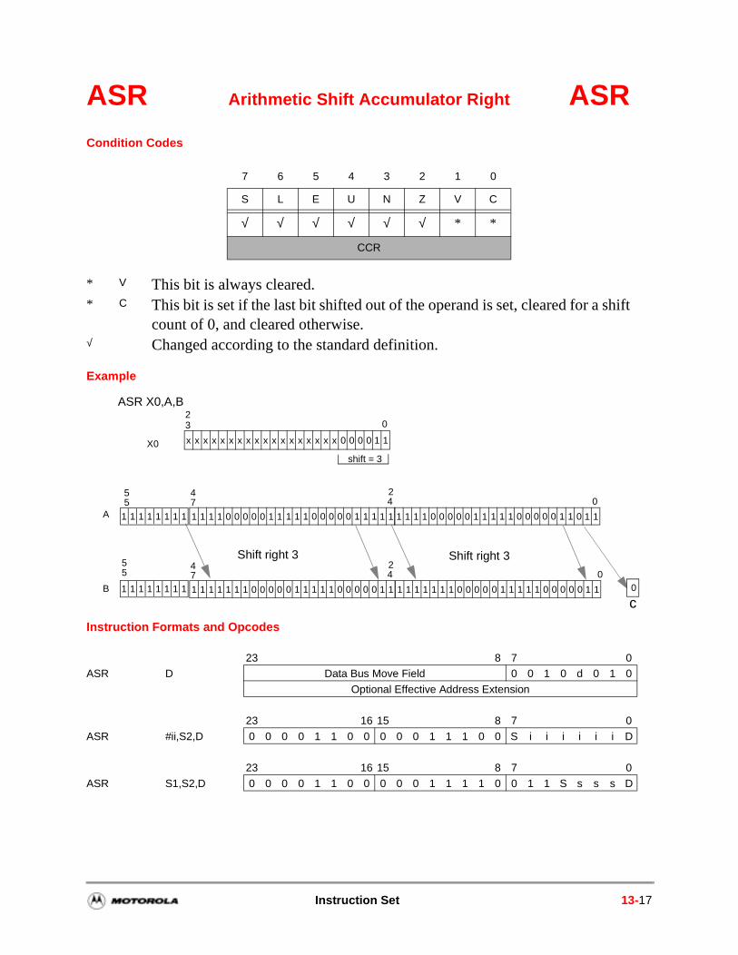
ASR Arithmetic Shift Accumulator Right ASRCondition Codes
Example
Instruction Formats and Opcodes
7 6 5 4 3 2 1 0
S L E U N Z V C
√ √ √ √ √ √ * *
CCR
* V This bit is always cleared.* C This bit is set if the last bit shifted out of the operand is set, cleared for a shift
count of 0, and cleared otherwise. √ Changed according to the standard definition.
23 8 7 0ASR D Data Bus Move Field 0 0 1 0 d 0 1 0
Optional Effective Address Extension
23 16 15 8 7 0
ASR #ii,S2,D 0 0 0 0 1 1 0 0 0 0 0 1 1 1 0 0 S i i i i i i D
23 16 15 8 7 0
ASR S1,S2,D 0 0 0 0 1 1 0 0 0 0 0 1 1 1 1 0 0 1 1 S s s s D
ASR X0,A,B
1 1 1 1 0 0 0 0 0 1 1 1 1 1 0 0 0 0 0 1 1 1 1 1
447
2
1 1 1 1 1 1 1 0 0 0 0 0 1 1 1 1 1 0 0 0 0 0 1 1
447
2
shift = 3
X0
1 1 1 1 0 0 0 0 0 1 1 1 1 1 0 0 0 0 0 1 1 0 1 1
0
1 1 1 1 1 1 1 0 0 0 0 0 1 1 1 1 1 0 0 0 0 0 1 1
0
Shift right 3 Shift right 3
A
B 0
c
1 1 1 1 1 1 1 1
1 1 1 1 1 1 1 1
55
55
x x x x x x x x x x x x x x x x x x 0 0 0 0 1 1
023
Instruction Set 13-17
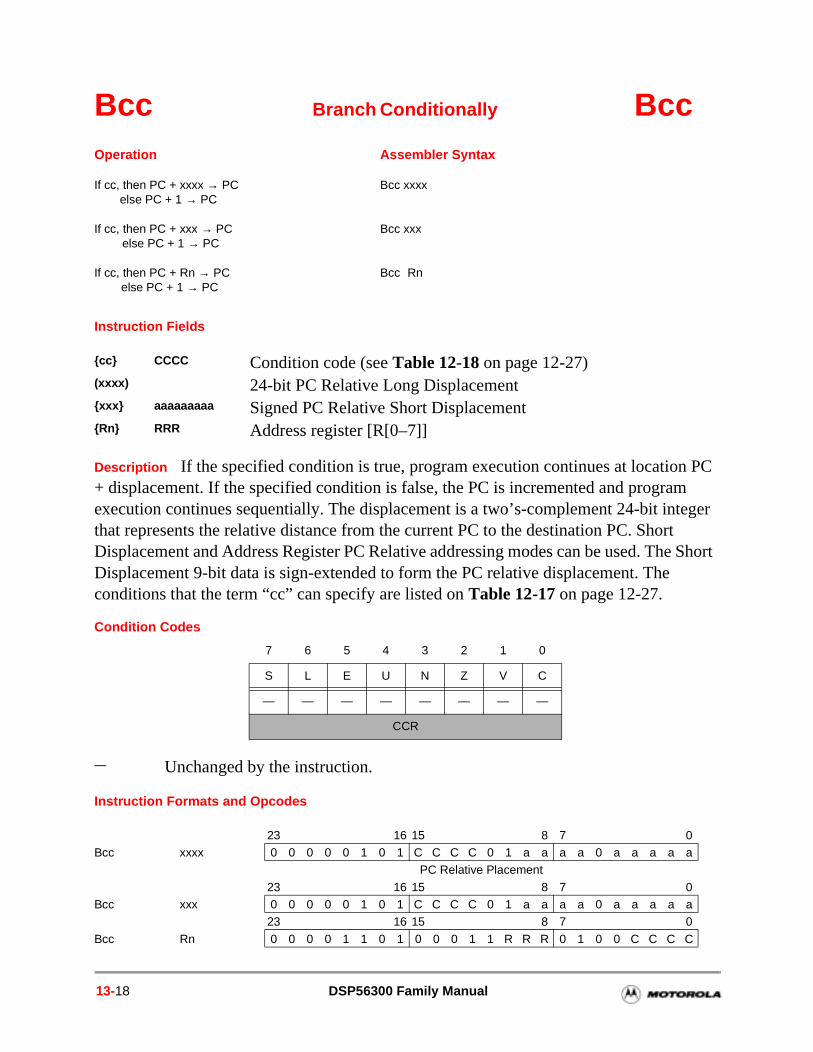
teger t e Short
Bcc Branch Conditionally Bcc
Instruction Fields
Description If the specified condition is true, program execution continues at location PC + displacement. If the specified condition is false, the PC is incremented and program execution continues sequentially. The displacement is a two’s-complement 24-bit inthat represents the relative distance from the current PC to the destination PC. ShorDisplacement and Address Register PC Relative addressing modes can be used. ThDisplacement 9-bit data is sign-extended to form the PC relative displacement. The conditions that the term “cc” can specify are listed on Table 12-17 on page 12-27.
Condition Codes
Instruction Formats and Opcodes
Operation Assembler Syntax
If cc, then PC + xxxx → PCelse PC + 1 → PC
Bcc xxxx
If cc, then PC + xxx → PC Bcc xxxelse PC + 1 → PC
If cc, then PC + Rn → PC Bcc Rnelse PC + 1 → PC
cc CCCC Condition code (see Table 12-18 on page 12-27)(xxxx) 24-bit PC Relative Long Displacementxxx aaaaaaaaa Signed PC Relative Short DisplacementRn RRR Address register [R[0–7]]
7 6 5 4 3 2 1 0
S L E U N Z V C
— — — — — — — —
CCR
— Unchanged by the instruction.
23 16 15 8 7 0Bcc xxxx 0 0 0 0 0 1 0 1 C C C C 0 1 a a a a 0 a a a a a
PC Relative Placement
23 16 15 8 7 0Bcc xxx 0 0 0 0 0 1 0 1 C C C C 0 1 a a a a 0 a a a a a
23 16 15 8 7 0
Bcc Rn 0 0 0 0 1 1 0 1 0 0 0 1 1 R R R 0 1 0 0 C C C C
13-18 DSP56300 Family Manual
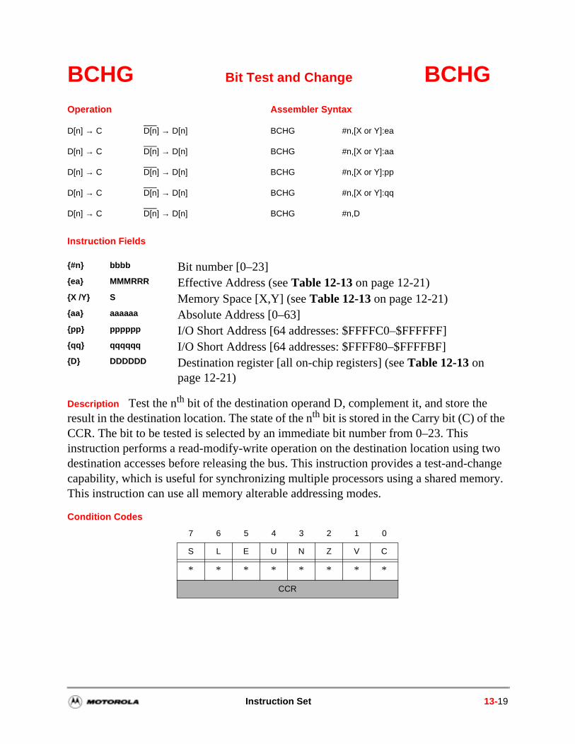
two hange ory.
BCHG Bit Test and Change BCHG
Instruction Fields
Description Test the nth bit of the destination operand D, complement it, and store the result in the destination location. The state of the nth bit is stored in the Carry bit (C) of the CCR. The bit to be tested is selected by an immediate bit number from 0–23. This instruction performs a read-modify-write operation on the destination location using destination accesses before releasing the bus. This instruction provides a test-and-ccapability, which is useful for synchronizing multiple processors using a shared memThis instruction can use all memory alterable addressing modes.
Condition Codes
Operation Assembler Syntax
D[n] → C D[n] → D[n] BCHG #n,[X or Y]:ea
D[n] → C D[n] → D[n] BCHG #n,[X or Y]:aa
D[n] → C D[n] → D[n] BCHG #n,[X or Y]:pp
D[n] → C D[n] → D[n] BCHG #n,[X or Y]:qq
D[n] → C D[n] → D[n] BCHG #n,D
#n bbbb Bit number [0–23]ea MMMRRR Effective Address (see Table 12-13 on page 12-21)X /Y S Memory Space [X,Y] (see Table 12-13 on page 12-21) aa aaaaaa Absolute Address [0–63]pp pppppp I/O Short Address [64 addresses: $FFFFC0–$FFFFFF]qq qqqqqq I/O Short Address [64 addresses: $FFFF80–$FFFFBF]D DDDDDD Destination register [all on-chip registers] (see Table 12-13 on
page 12-21)
7 6 5 4 3 2 1 0
S L E U N Z V C
* * * * * * * *
CCR
Instruction Set 13-19
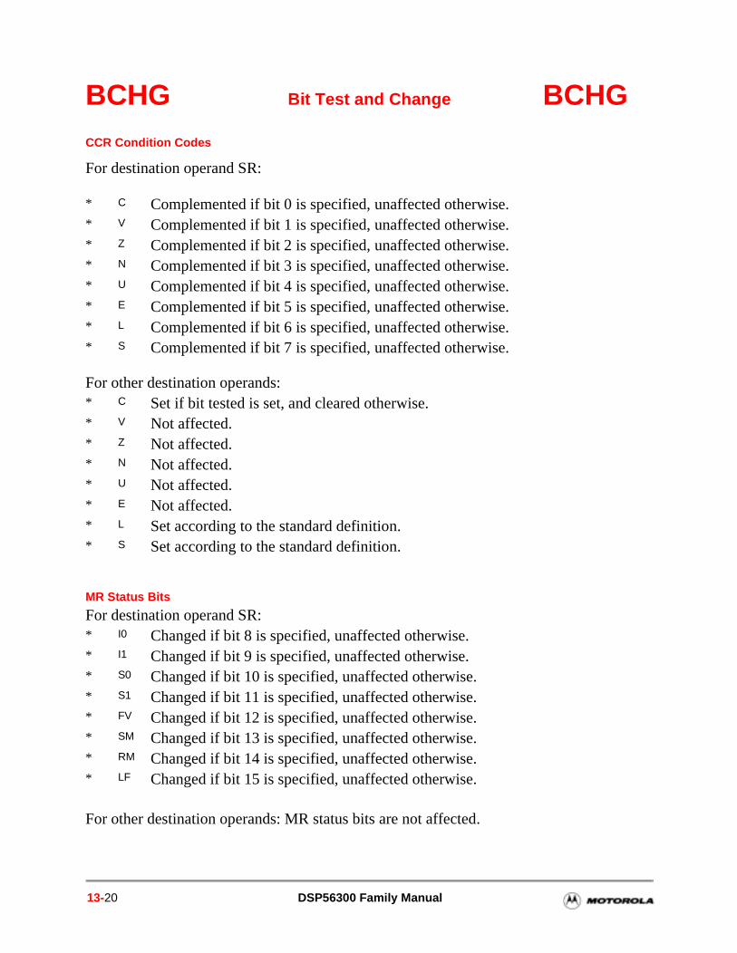
BCHG Bit Test and Change BCHGCCR Condition Codes
For destination operand SR:
* C Complemented if bit 0 is specified, unaffected otherwise.* V Complemented if bit 1 is specified, unaffected otherwise.* Z Complemented if bit 2 is specified, unaffected otherwise.* N Complemented if bit 3 is specified, unaffected otherwise.* U Complemented if bit 4 is specified, unaffected otherwise.* E Complemented if bit 5 is specified, unaffected otherwise.* L Complemented if bit 6 is specified, unaffected otherwise.* S Complemented if bit 7 is specified, unaffected otherwise.
For other destination operands:* C Set if bit tested is set, and cleared otherwise.* V Not affected.* Z Not affected.* N Not affected.* U Not affected.* E Not affected.* L Set according to the standard definition.* S Set according to the standard definition.
MR Status Bits
For destination operand SR: * I0 Changed if bit 8 is specified, unaffected otherwise.* I1 Changed if bit 9 is specified, unaffected otherwise.* S0 Changed if bit 10 is specified, unaffected otherwise.* S1 Changed if bit 11 is specified, unaffected otherwise.* FV Changed if bit 12 is specified, unaffected otherwise.* SM Changed if bit 13 is specified, unaffected otherwise.* RM Changed if bit 14 is specified, unaffected otherwise.* LF Changed if bit 15 is specified, unaffected otherwise.
For other destination operands: MR status bits are not affected.
13-20 DSP56300 Family Manual
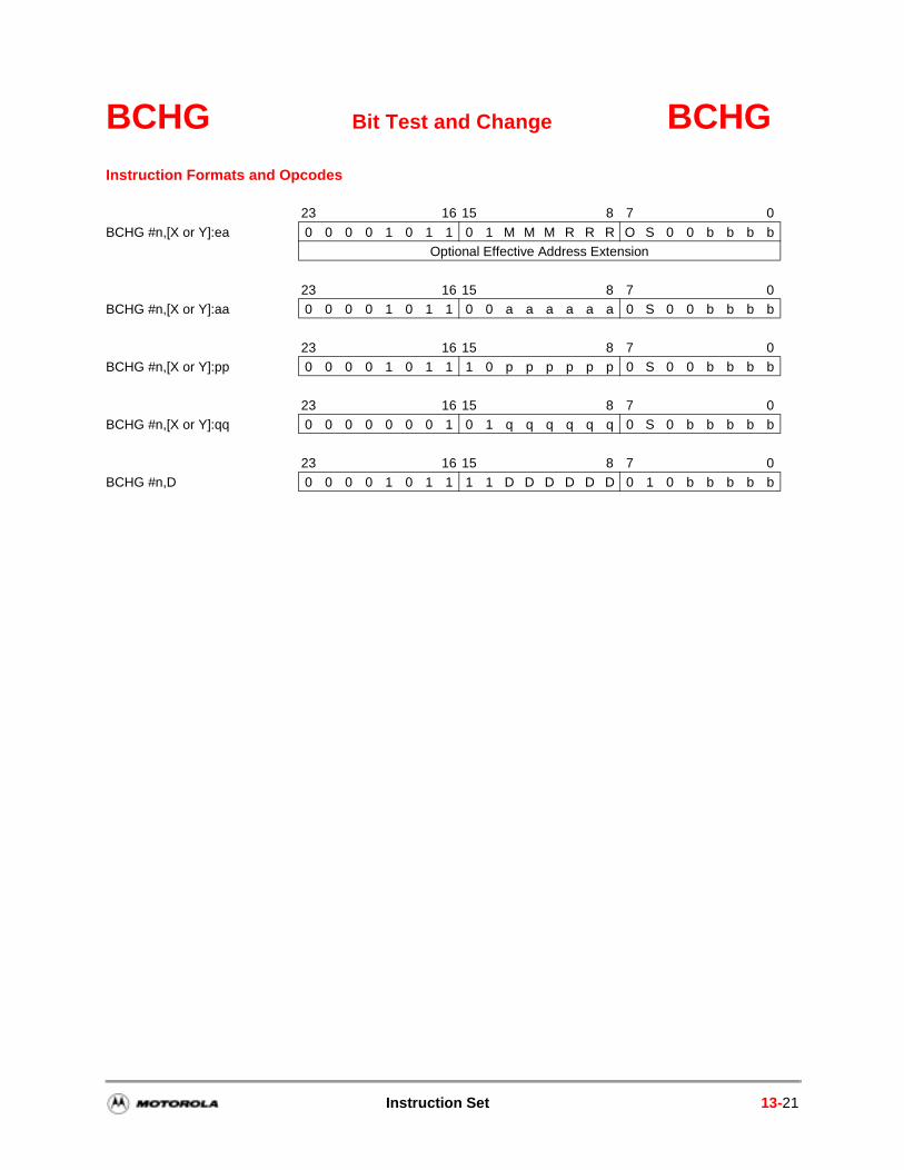
BCHG Bit Test and Change BCHGInstruction Formats and Opcodes
23 16 15 8 7 0
BCHG #n,[X or Y]:ea 0 0 0 0 1 0 1 1 0 1 M M M R R R O S 0 0 b b b bOptional Effective Address Extension
23 16 15 8 7 0BCHG #n,[X or Y]:aa 0 0 0 0 1 0 1 1 0 0 a a a a a a 0 S 0 0 b b b b
23 16 15 8 7 0BCHG #n,[X or Y]:pp 0 0 0 0 1 0 1 1 1 0 p p p p p p 0 S 0 0 b b b b
23 16 15 8 7 0BCHG #n,[X or Y]:qq 0 0 0 0 0 0 0 1 0 1 q q q q q q 0 S 0 b b b b b
23 16 15 8 7 0BCHG #n,D 0 0 0 0 1 0 1 1 1 1 D D D D D D 0 1 0 b b b b b
Instruction Set 13-21
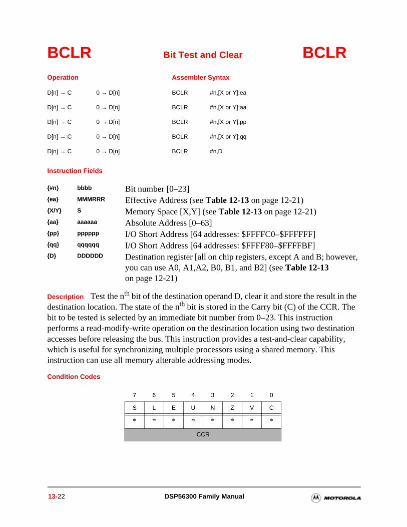
tion lity,
ver,
BCLR Bit Test and Clear BCLR
Instruction Fields
Description Test the nth bit of the destination operand D, clear it and store the result in the destination location. The state of the nth bit is stored in the Carry bit (C) of the CCR. The bit to be tested is selected by an immediate bit number from 0–23. This instruction performs a read-modify-write operation on the destination location using two destinaaccesses before releasing the bus. This instruction provides a test-and-clear capabiwhich is useful for synchronizing multiple processors using a shared memory. This instruction can use all memory alterable addressing modes.
Condition Codes
Operation Assembler Syntax
D[n] → C 0 → D[n] BCLR #n,[X or Y]:ea
D[n] → C 0 → D[n] BCLR #n,[X or Y]:aa
D[n] → C 0 → D[n] BCLR #n,[X or Y]:pp
D[n] → C 0 → D[n] BCLR #n,[X or Y]:qq
D[n] → C 0 → D[n] BCLR #n,D
#n bbbb Bit number [0–23]ea MMMRRR Effective Address (see Table 12-13 on page 12-21)X/Y S Memory Space [X,Y] (see Table 12-13 on page 12-21)aa aaaaaa Absolute Address [0–63]pp pppppp I/O Short Address [64 addresses: $FFFFC0–$FFFFFF]qq qqqqqq I/O Short Address [64 addresses: $FFFF80–$FFFFBF]D DDDDDD Destination register [all on chip registers, except A and B; howe
you can use A0, A1,A2, B0, B1, and B2] (see Table 12-13 on page 12-21)
7 6 5 4 3 2 1 0
S L E U N Z V C
* * * * * * * *
CCR
13-22 DSP56300 Family Manual
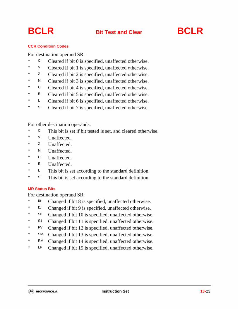
BCLR Bit Test and Clear BCLRCCR Condition Codes
For destination operand SR: * C Cleared if bit 0 is specified, unaffected otherwise.* V Cleared if bit 1 is specified, unaffected otherwise.* Z Cleared if bit 2 is specified, unaffected otherwise.* N Cleared if bit 3 is specified, unaffected otherwise.* U Cleared if bit 4 is specified, unaffected otherwise.* E Cleared if bit 5 is specified, unaffected otherwise.* L Cleared if bit 6 is specified, unaffected otherwise.* S Cleared if bit 7 is specified, unaffected otherwise.
For other destination operands:* C This bit is set if bit tested is set, and cleared otherwise.* V Unaffected.* Z Unaffected.* N Unaffected.* U Unaffected.* E Unaffected.* L This bit is set according to the standard definition.* S This bit is set according to the standard definition.
MR Status Bits
For destination operand SR: * I0 Changed if bit 8 is specified, unaffected otherwise.* I1 Changed if bit 9 is specified, unaffected otherwise.* S0 Changed if bit 10 is specified, unaffected otherwise.* S1 Changed if bit 11 is specified, unaffected otherwise.* FV Changed if bit 12 is specified, unaffected otherwise.* SM Changed if bit 13 is specified, unaffected otherwise.* RM Changed if bit 14 is specified, unaffected otherwise.* LF Changed if bit 15 is specified, unaffected otherwise.
Instruction Set 13-23
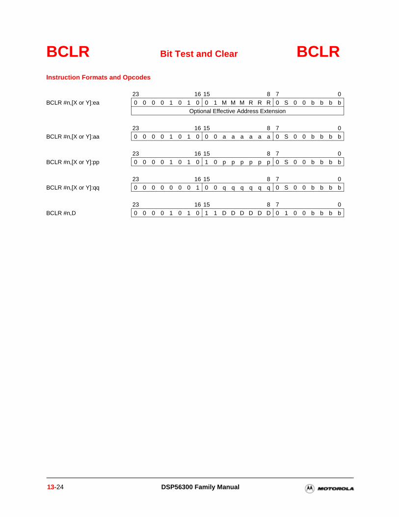
BCLR Bit Test and Clear BCLRInstruction Formats and Opcodes
23 16 15 8 7 0
BCLR #n,[X or Y]:ea 0 0 0 0 1 0 1 0 0 1 M M M R R R 0 S 0 0 b b b bOptional Effective Address Extension
23 16 15 8 7 0BCLR #n,[X or Y]:aa 0 0 0 0 1 0 1 0 0 0 a a a a a a 0 S 0 0 b b b b
23 16 15 8 7 0BCLR #n,[X or Y]:pp 0 0 0 0 1 0 1 0 1 0 p p p p p p 0 S 0 0 b b b b
23 16 15 8 7 0BCLR #n,[X or Y]:qq 0 0 0 0 0 0 0 1 0 0 q q q q q q 0 S 0 0 b b b b
23 16 15 8 7 0BCLR #n,D 0 0 0 0 1 0 1 0 1 1 D D D D D D 0 1 0 0 b b b b
13-24 DSP56300 Family Manual
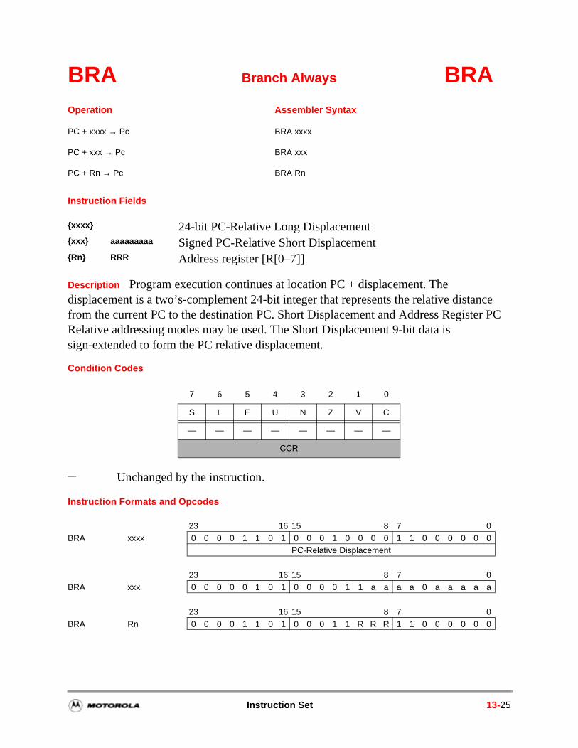
ce r PC
BRA Branch Always BRA
Instruction Fields
Description Program execution continues at location PC + displacement. The displacement is a two’s-complement 24-bit integer that represents the relative distanfrom the current PC to the destination PC. Short Displacement and Address RegisteRelative addressing modes may be used. The Short Displacement 9-bit data is sign-extended to form the PC relative displacement.
Condition Codes
Instruction Formats and Opcodes
Operation Assembler Syntax
PC + xxxx → Pc BRA xxxx
PC + xxx → Pc BRA xxx
PC + Rn → Pc BRA Rn
xxxx 24-bit PC-Relative Long Displacementxxx aaaaaaaaa Signed PC-Relative Short DisplacementRn RRR Address register [R[0–7]]
7 6 5 4 3 2 1 0
S L E U N Z V C
— — — — — — — —
CCR
— Unchanged by the instruction.
23 16 15 8 7 0BRA xxxx 0 0 0 0 1 1 0 1 0 0 0 1 0 0 0 0 1 1 0 0 0 0 0 0
PC-Relative Displacement
23 16 15 8 7 0BRA xxx 0 0 0 0 0 1 0 1 0 0 0 0 1 1 a a a a 0 a a a a a
23 16 15 8 7 0BRA Rn 0 0 0 0 1 1 0 1 0 0 0 1 1 R R R 1 1 0 0 0 0 0 0
Instruction Set 13-25
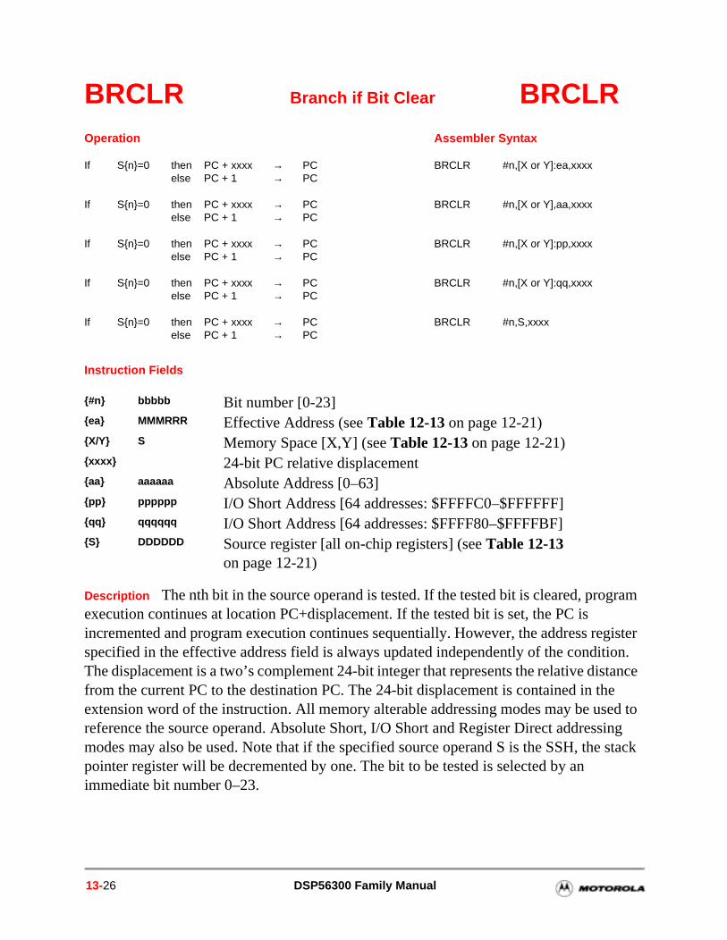
stance e ed to sing e stack
BRCLR Branch if Bit Clear BRCLR
Instruction Fields
Description The nth bit in the source operand is tested. If the tested bit is cleared, program execution continues at location PC+displacement. If the tested bit is set, the PC is incremented and program execution continues sequentially. However, the address register specified in the effective address field is always updated independently of the condition. The displacement is a two’s complement 24-bit integer that represents the relative difrom the current PC to the destination PC. The 24-bit displacement is contained in thextension word of the instruction. All memory alterable addressing modes may be usreference the source operand. Absolute Short, I/O Short and Register Direct addresmodes may also be used. Note that if the specified source operand S is the SSH, thpointer register will be decremented by one. The bit to be tested is selected by an immediate bit number 0–23.
Operation Assembler Syntax
If Sn=0 then PC + xxxx → PC BRCLR #n,[X or Y]:ea,xxxxelse PC + 1 → PC
If Sn=0 then PC + xxxx → PC BRCLR #n,[X or Y],aa,xxxxelse PC + 1 → PC
If Sn=0 then PC + xxxx → PC BRCLR #n,[X or Y]:pp,xxxxelse PC + 1 → PC
If Sn=0 then PC + xxxx → PC BRCLR #n,[X or Y]:qq,xxxxelse PC + 1 → PC
If Sn=0 then PC + xxxx → PC BRCLR #n,S,xxxxelse PC + 1 → PC
#n bbbbb Bit number [0-23]ea MMMRRR Effective Address (see Table 12-13 on page 12-21)X/Y S Memory Space [X,Y] (see Table 12-13 on page 12-21)xxxx 24-bit PC relative displacementaa aaaaaa Absolute Address [0–63]pp pppppp I/O Short Address [64 addresses: $FFFFC0–$FFFFFF]qq qqqqqq I/O Short Address [64 addresses: $FFFF80–$FFFFBF]S DDDDDD Source register [all on-chip registers] (see Table 12-13
on page 12-21)
13-26 DSP56300 Family Manual
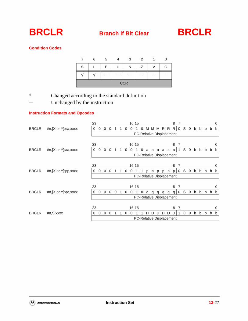
BRCLR Branch if Bit Clear BRCLRCondition Codes
Instruction Formats and Opcodes
7 6 5 4 3 2 1 0
S L E U N Z V C
√ √ — — — — — —
CCR
√ Changed according to the standard definition— Unchanged by the instruction
23 16 15 8 7 0BRCLR #n,[X or Y]:ea,xxxx 0 0 0 0 1 1 0 0 1 0 M M M R R R 0 S 0 b b b b b
PC-Relative Displacement
23 16 15 8 7 0BRCLR #n,[X or Y]:aa,xxxx 0 0 0 0 1 1 0 0 1 0 a a a a a a 1 S 0 b b b b b
PC-Relative Displacement
23 16 15 8 7 0
BRCLR #n,[X or Y]:pp,xxxx 0 0 0 0 1 1 0 0 1 1 p p p p p p 0 S 0 b b b b bPC-Relative Displacement
23 16 15 8 7 0BRCLR #n,[X or Y]:qq,xxxx 0 0 0 0 0 1 0 0 1 0 q q q q q q 0 S 0 b b b b b
PC-Relative Displacement
23 16 15 8 7 0BRCLR #n,S,xxxx 0 0 0 0 1 1 0 0 1 1 D D D D D D 1 0 0 b b b b b
PC-Relative Displacement
Instruction Set 13-27
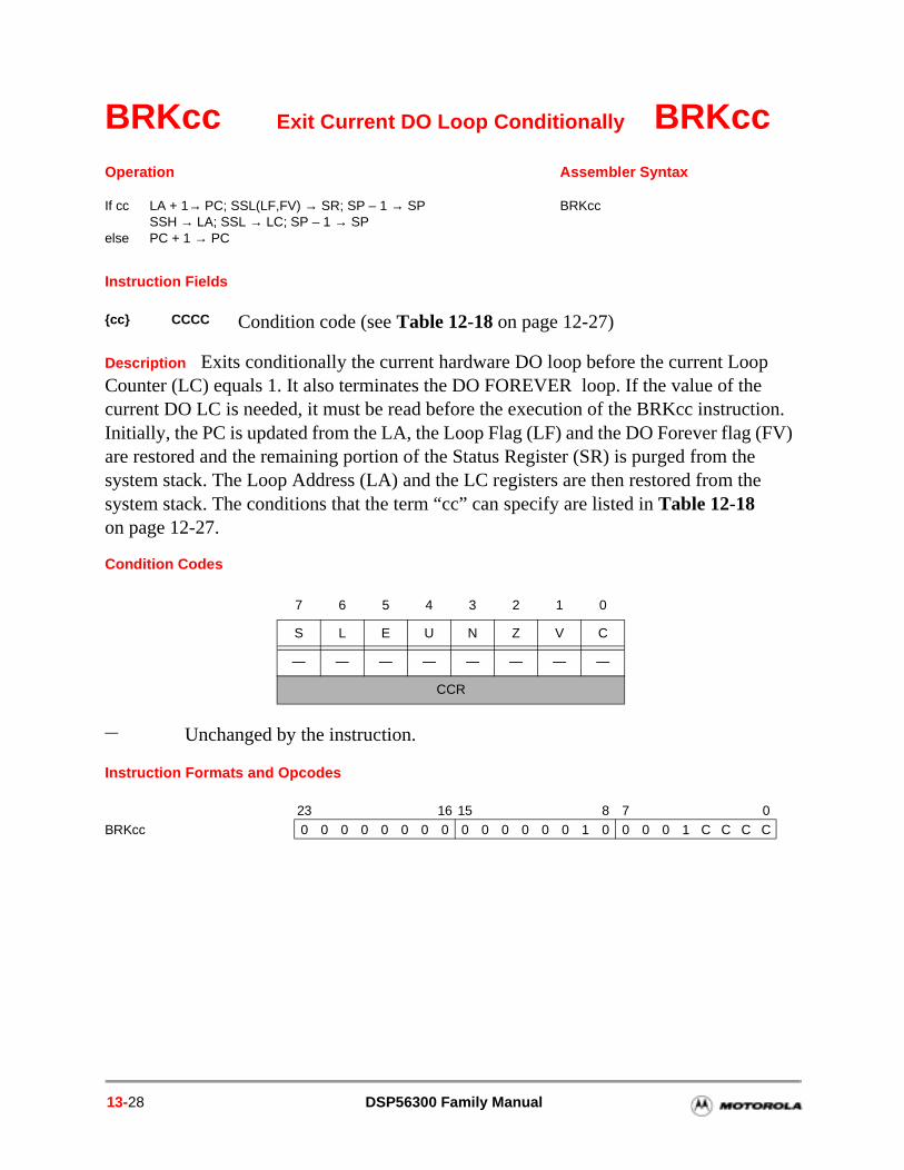
BRKcc Exit Current DO Loop Conditionally BRKcc
Instruction Fields
Description Exits conditionally the current hardware DO loop before the current Loop Counter (LC) equals 1. It also terminates the DO FOREVER loop. If the value of the current DO LC is needed, it must be read before the execution of the BRKcc instruction. Initially, the PC is updated from the LA, the Loop Flag (LF) and the DO Forever flag (FV) are restored and the remaining portion of the Status Register (SR) is purged from the system stack. The Loop Address (LA) and the LC registers are then restored from the system stack. The conditions that the term “cc” can specify are listed in Table 12-18 on page 12-27.
Condition Codes
Instruction Formats and Opcodes
Operation Assembler Syntax
If cc LA + 1→ PC; SSL(LF,FV) → SR; SP – 1 → SP BRKccSSH → LA; SSL → LC; SP – 1 → SP
else PC + 1 → PC
cc CCCC Condition code (see Table 12-18 on page 12-27)
7 6 5 4 3 2 1 0
S L E U N Z V C
— — — — — — — —
CCR
— Unchanged by the instruction.
23 16 15 8 7 0BRKcc 0 0 0 0 0 0 0 0 0 0 0 0 0 0 1 0 0 0 0 1 C C C C
13-28 DSP56300 Family Manual
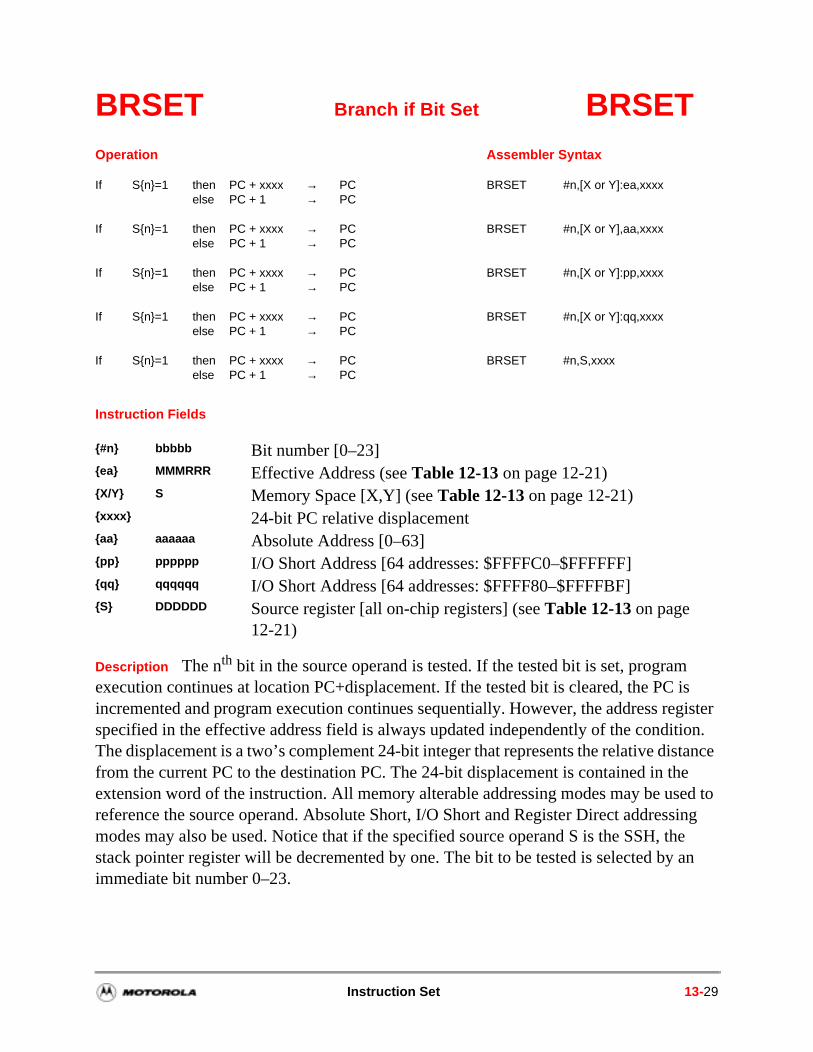
stance e ed to sing the an
BRSET Branch if Bit Set BRSET
Instruction Fields
Description The nth bit in the source operand is tested. If the tested bit is set, program execution continues at location PC+displacement. If the tested bit is cleared, the PC is incremented and program execution continues sequentially. However, the address register specified in the effective address field is always updated independently of the condition. The displacement is a two’s complement 24-bit integer that represents the relative difrom the current PC to the destination PC. The 24-bit displacement is contained in thextension word of the instruction. All memory alterable addressing modes may be usreference the source operand. Absolute Short, I/O Short and Register Direct addresmodes may also be used. Notice that if the specified source operand S is the SSH, stack pointer register will be decremented by one. The bit to be tested is selected byimmediate bit number 0–23.
Operation Assembler Syntax
If Sn=1 then PC + xxxx → PC BRSET #n,[X or Y]:ea,xxxxelse PC + 1 → PC
If Sn=1 then PC + xxxx → PC BRSET #n,[X or Y],aa,xxxxelse PC + 1 → PC
If Sn=1 then PC + xxxx → PC BRSET #n,[X or Y]:pp,xxxxelse PC + 1 → PC
If Sn=1 then PC + xxxx → PC BRSET #n,[X or Y]:qq,xxxxelse PC + 1 → PC
If Sn=1 then PC + xxxx → PC BRSET #n,S,xxxxelse PC + 1 → PC
#n bbbbb Bit number [0–23]ea MMMRRR Effective Address (see Table 12-13 on page 12-21)X/Y S Memory Space [X,Y] (see Table 12-13 on page 12-21)xxxx 24-bit PC relative displacementaa aaaaaa Absolute Address [0–63]pp pppppp I/O Short Address [64 addresses: $FFFFC0–$FFFFFF]qq qqqqqq I/O Short Address [64 addresses: $FFFF80–$FFFFBF]S DDDDDD Source register [all on-chip registers] (see Table 12-13 on page
12-21)
Instruction Set 13-29
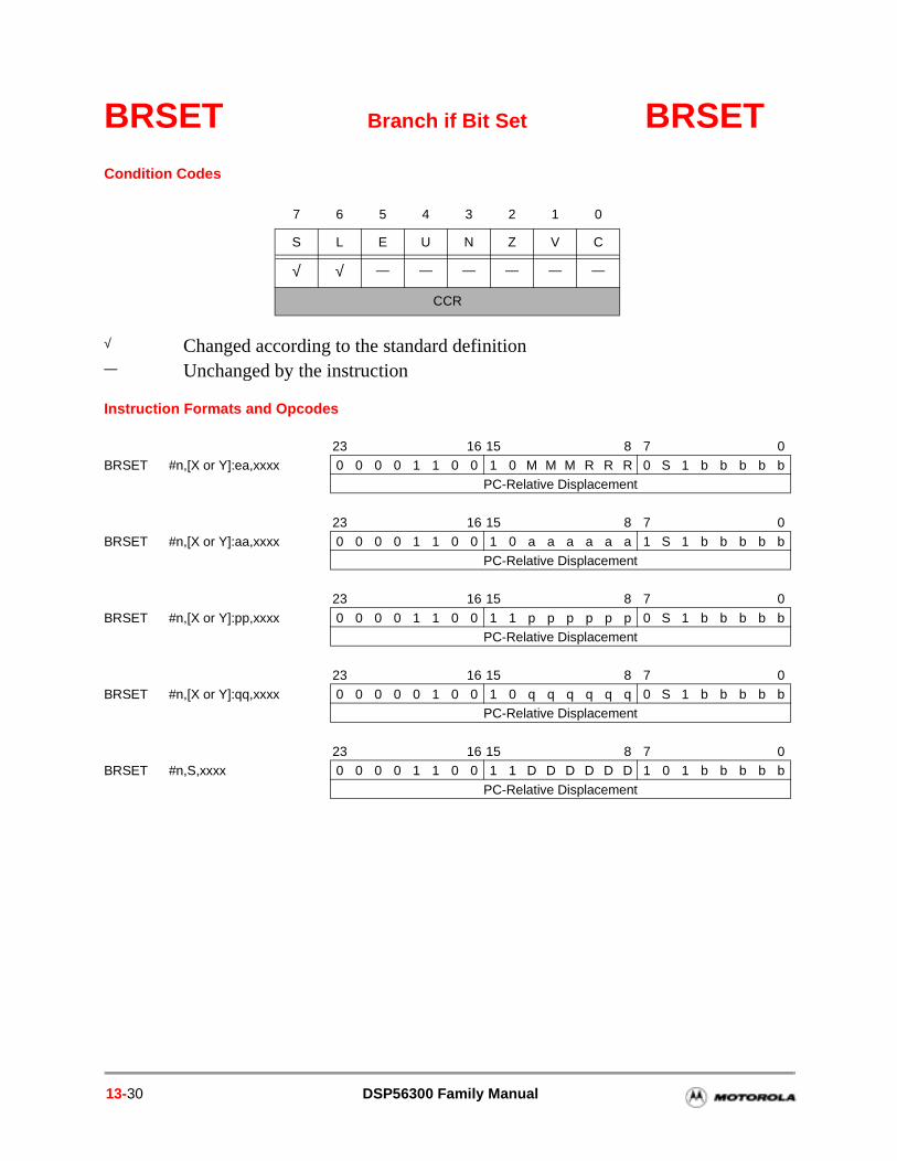
BRSET Branch if Bit Set BRSETCondition Codes
Instruction Formats and Opcodes
7 6 5 4 3 2 1 0
S L E U N Z V C
√ √ — — — — — —
CCR
√ Changed according to the standard definition— Unchanged by the instruction
23 16 15 8 7 0BRSET #n,[X or Y]:ea,xxxx 0 0 0 0 1 1 0 0 1 0 M M M R R R 0 S 1 b b b b b
PC-Relative Displacement
23 16 15 8 7 0BRSET #n,[X or Y]:aa,xxxx 0 0 0 0 1 1 0 0 1 0 a a a a a a 1 S 1 b b b b b
PC-Relative Displacement
23 16 15 8 7 0
BRSET #n,[X or Y]:pp,xxxx 0 0 0 0 1 1 0 0 1 1 p p p p p p 0 S 1 b b b b bPC-Relative Displacement
23 16 15 8 7 0BRSET #n,[X or Y]:qq,xxxx 0 0 0 0 0 1 0 0 1 0 q q q q q q 0 S 1 b b b b b
PC-Relative Displacement
23 16 15 8 7 0BRSET #n,S,xxxx 0 0 0 0 1 1 0 0 1 1 D D D D D D 1 0 1 b b b b b
PC-Relative Displacement
13-30 DSP56300 Family Manual
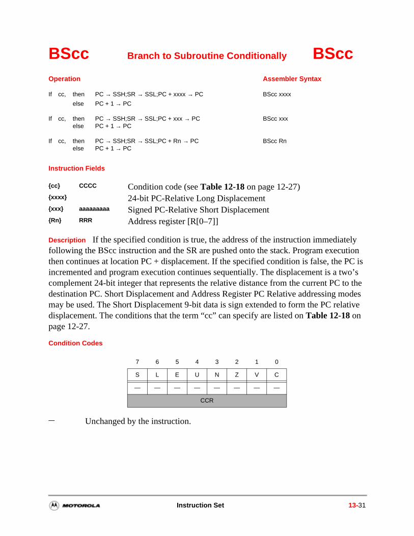
wo’s to the odes
lative
BScc Branch to Subroutine Conditionally BScc
Instruction Fields
Description If the specified condition is true, the address of the instruction immediately following the BScc instruction and the SR are pushed onto the stack. Program execution then continues at location PC + displacement. If the specified condition is false, the PC is incremented and program execution continues sequentially. The displacement is a tcomplement 24-bit integer that represents the relative distance from the current PC destination PC. Short Displacement and Address Register PC Relative addressing mmay be used. The Short Displacement 9-bit data is sign extended to form the PC redisplacement. The conditions that the term “cc” can specify are listed on Table 12-18 on page 12-27.
Condition Codes
Operation Assembler Syntax
If cc, then PC → SSH;SR → SSL;PC + xxxx → PC BScc xxxx
else PC + 1 → PC
If cc, then PC → SSH;SR → SSL;PC + xxx → PC BScc xxxelse PC + 1 → PC
If cc, then PC → SSH;SR → SSL;PC + Rn → PC BScc Rnelse PC + 1 → PC
cc CCCC Condition code (see Table 12-18 on page 12-27)xxxx 24-bit PC-Relative Long Displacementxxx aaaaaaaaa Signed PC-Relative Short DisplacementRn RRR Address register [R[0–7]]
7 6 5 4 3 2 1 0
S L E U N Z V C
— — — — — — — —
CCR
— Unchanged by the instruction.
Instruction Set 13-31
BScc Branch to Subroutine Conditionally BSccInstruction Formats and Opcodes
23 16 15 8 7 0
BScc xxxx 0 0 0 0 1 1 0 1 0 0 0 1 0 0 0 0 0 0 0 0 C C C CPC-Relative Displacement
23 16 15 8 7 0BScc xxx 0 0 0 0 0 1 0 1 C C C C 0 0 a a a a 0 a a a a a
23 16 15 8 7 0BScc Rn 0 0 0 0 1 1 0 1 0 0 0 1 1 R R R 0 0 0 0 C C C C
13-32 DSP56300 Family Manual
to the
nd. Note nts by
BSCLR Branch to Subroutine if Bit Clear BSCLR
Instruction Fields
Description The nth bit in the source operand is tested. If the tested bit is cleared, the address of the instruction immediately following the BSCLR instruction and the status register are pushed onto the stack. Program execution then continues at location PC+displacement. If the tested bit is set, the PC is incremented and program execution continues sequentially. However, the address register specified in the effective address field is always updated independently of the condition. The displacement is a two’s complement 24-bit integer that represents the relative distance from the current PC destination PC. The 24-bit displacement is contained in the extension word of the instruction. All memory alterable addressing modes can reference the source operaAbsolute Short, I/O Short and Register Direct addressing modes can also be used. that if the specified source operand S is the SSH, the stack pointer register decreme
Operation Assembler Syntax
If Sn=0 then PC → SSH;SR → SSL;PC+xxxx → PC BSCLR #n,[X or Y]:ea,xxxxelse PC+1 → PC
If Sn=0 then PC → SSH;SR → SSL;PC+xxxx → PC BSCLR #n,[X or Y],aa,xxxxelse PC+1 → PC
If Sn=0 then PC → SSH;SR → SSL;PC+xxxx → PC BSCLR #n,[X or Y]:pp,xxxxelse PC+1 → PC
If Sn=0 then PC → SSH;SR → SSL;PC+xxxx → PC BSCLR #n,[X or Y]:qq,xxxxelse PC+1 → PC
If Sn=0 then PC → SSH;SR → SSL;PC+xxxx → PC BSCLR #n,S,xxxxelse PC+1 → PC
#n bbbbb Bit number [0–23]ea MMMRRR Effective Address (see Table 12-13 on page 12-21)X/Y S Memory Space [X,Y] (see Table 12-13 on page 12-21)xxxx 24-bit Relative Long Displacementaa aaaaaa Absolute Address [0-63]pp pppppp I/O Short Address [64 addresses: $FFFFC0–$FFFFFF]qq qqqqqq I/O Short Address [64 addresses: $FFFF80–$FFFFBF]S DDDDDD Source register [all on-chip registers](see Table 12-13 on page
12-21)
Instruction Set 13-33
BSCLR Branch to Subroutine if Bit Clear BSCLR
one; if the condition is true, the push operation writes over the stack level where the SSH value is taken. The bit to be tested is selected by an immediate bit number 0–23.
Condition Codes
Instruction Formats and Opcodes
7 6 5 4 3 2 1 0
S L E U N Z V C
√ √ — — — — — —
CCR
√ Changed according to the standard definition— Unchanged by the instruction
23 16 15 8 7 0BSCLR #n,[X or Y]:ea,xxxx 0 0 0 0 1 1 0 1 1 0 M M M R R R 0 S 0 b b b b b
PC-Relative Displacement
23 16 15 8 7 0BSCLR #n,[X or Y]:aa,xxxx 0 0 0 0 1 1 0 1 1 0 a a a a a a 1 S 0 b b b b b
PC-Relative Displacement
23 16 15 8 7 0
BSCLR #n,[X or Y]:qq,xxxx 0 0 0 0 0 1 0 0 1 0 q q q q q q 1 S 0 b b b b bPC-Relative Displacement
23 16 15 8 7 0BSCLR #n,[X or Y]:pp,xxxx 0 0 0 0 1 1 0 1 1 1 p p p p p p 0 S 0 b b b b b
PC-Relative Displacement
23 16 15 8 7 0BSCLR #n,S,xxxx 0 0 0 0 1 1 0 1 1 1 D D D D D D 1 0 0 b b b b b
PC-Relative Displacement
13-34 DSP56300 Family Manual
tion that is
n can
egister
er,
BSET Bit Set and Test BSET
Instruction Fields
Description Test the nth bit of the destination operand D, set it, and store the result in the destination location. The state of the nth bit is stored in the Carry bit (C) of the CCR. The bit to be tested is selected by an immediate bit number from 0–23. This instruction performs a read-modify-write operation on the destination location using two destinaaccesses before releasing the bus. This instruction provides a test-and-set capabilityuseful for synchronizing multiple processors using a shared memory. This instructiouse all memory alterable addressing modes. When this instruction performs a bit manipulation/test on either the A or B 56-bit accumulator, it optionally shifts the accumulator value according to scaling mode bits S0 and S1 in the system Status R(SR). If the data out of the shifter indicates that the accumulator extension
register is in use, the instruction acts on the limited value (limited on the maximum positive or negative saturation constant). The “L” flag in the SR is set accordingly.
Operation Assembler Syntax
D[n] → C 1 → D[n] BSET #n,[X or Y]:ea
D[n] → C 1 → D[n] BSET #n,[X or Y]:aa
D[n] → C 1 → D[n] BSET #n,[X or Y]:pp
D[n] → C 1 → D[n] BSET #n,[X or Y]:qq
D[n] → C 1 → D[n] BSET #n,D
#n bbbb Bit number [0–23] ea MMMRRR Effective Address (see Table 12-13 on page 12-21)X/Y S Memory Space [X,Y] (see Table 12-13 on page 12-21)aa aaaaaa Absolute Address [0–63]pp pppppp I/O Short Address [64 addresses: $FFFFC0–$FFFFFF]qq qqqqqq I/O Short Address [64 addresses: $FFFF80–$FFFFBF]D DDDDDD Destination register [all on chip registers, except A and B; howev
you can use A0, A1, A2, B0, B1, and B2] (see Table 12-13 on page 12-21)
Instruction Set 13-35
BSET Bit Set and Test BSETCondition Codes
7 6 5 4 3 2 1 0
S L E U N Z V C
* * * * * * * *
CCR
CCR Condition Codes
For destination operand SR: * C Set if bit 0 is specified, unaffected otherwise.* V Set if bit 1 is specified, unaffected otherwise.* Z Set if bit 2 is specified, unaffected otherwise.* N Set if bit 3 is specified, unaffected otherwise.* U Set if bit 4 is specified, unaffected otherwise.* E Set if bit 5 is specified, unaffected otherwise.* L Set if bit 6 is specified, unaffected otherwise.* S Set if bit 7 is specified, unaffected otherwise.
For other destination operands:* C Set if bit tested is set, and cleared otherwise.* V Unaffected.* Z Unaffected.* N Unaffected.* U Unaffected.* E Unaffected.* L Set according to the standard definition.* S Set according to the standard definition.
13-36 DSP56300 Family Manual
BSET Bit Set and Test BSET
MR Status Bits
For destination operand SR: * I0 Changed if bit 8 is specified, unaffected otherwise. * I1 Changed if bit 9 is specified, unaffected otherwise. * S0 Changed if bit 10 is specified, unaffected otherwise. * S1 Changed if bit 11 is specified, unaffected otherwise. * FV Changed if bit 12 is specified, unaffected otherwise. * SM Changed if bit 13 is specified, unaffected otherwise. * RM Changed if bit 14 is specified, unaffected otherwise.* LF Changed if bit 15 is specified, unaffected otherwise.
For other destination operands: MR status bits are not affected.
Instruction Formats and Opcodes
23 16 15 8 7 0BSET #n,[X or Y]:ea 0 0 0 0 1 0 1 0 0 1 M M M R R R 0 S 1 0 b b b b
OPTIONAL EFFECTIVE ADDRESS EXTENSION
23 16 15 8 7 0
BSET #n,[X or Y]:aa 0 0 0 0 1 0 1 0 0 0 a a a a a a 0 S 1 0 b b b b
23 16 15 8 7 0
BSET #n,[X or Y]:pp 0 0 0 0 1 0 1 0 1 0 p p p p p p 0 S 1 0 b b b b
23 16 15 8 7 0
BSET #n,[X or Y]:qq 0 0 0 0 0 0 0 1 0 0 q q q q q q 0 S 1 0 b b b b
23 16 15 8 7 0
BSET #n,D 0 0 0 0 1 0 1 0 1 1 D D D D D D 0 1 1 0 b b b b
Instruction Set 13-37
e ent
BSR Branch to Subroutine BSR
Instruction Fields
Description The address of the instruction immediately following the BSR instruction and the SR are pushed onto the stack. Program execution then continues at location PC + displacement. The displacement is a two’s-complement 24-bit integer that represents threlative distance from the current PC to the destination PC. Short Displacement andAddress Register PC-Relative addressing modes can be used. The Short Displacem9-bit data is sign-extended to form the PC-Relative displacement.
Condition Codes
Instruction Formats and Opcodes
Operation Assembler Syntax
PC → SSH;SR → SSL;PC + xxxx → PC BSR xxxx
PC → SSH;SR → SSL;PC + xxx → PC BSR xxx
PC → SSH;SR → SSL;PC + Rn → PC BSR Rn
xxxx 24-bit PC-Relative Long Displacementxxx aaaaaaaaa Signed PC-Relative Short DisplacementRn RRR Address register [R[0–7]]
7 6 5 4 3 2 1 0
S L E U N Z V C
— — — — — — — —
CCR
— Unchanged by the instruction.
23 16 15 8 7 0BSR xxxx 0 0 0 0 1 1 0 1 0 0 0 1 0 0 0 0 1 0 0 0 0 0 0 0
PC-Relative Displacement
23 16 15 8 7 0
BSR xxx 0 0 0 0 0 1 0 1 0 0 0 0 1 0 a a a a 0 a a a a a
23 16 15 8 7 0BSR Rn 0 0 0 0 1 1 0 1 0 0 0 1 1 R R R 1 0 0 0 0 0 0 0
13-38 DSP56300 Family Manual
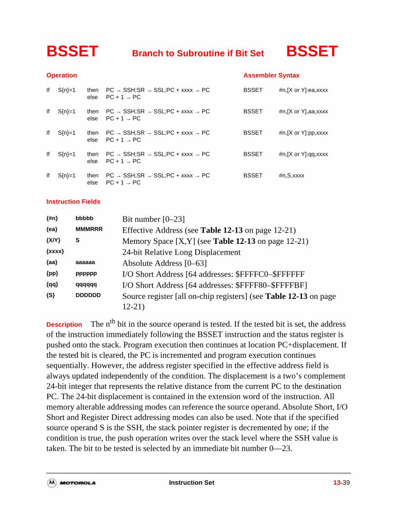
ment tion
ll ort, I/O ified e is
BSSET Branch to Subroutine if Bit Set BSSET
Instruction Fields
Description The nth bit in the source operand is tested. If the tested bit is set, the address of the instruction immediately following the BSSET instruction and the status register is pushed onto the stack. Program execution then continues at location PC+displacement. If the tested bit is cleared, the PC is incremented and program execution continues sequentially. However, the address register specified in the effective address field is always updated independently of the condition. The displacement is a two’s comple24-bit integer that represents the relative distance from the current PC to the destinaPC. The 24-bit displacement is contained in the extension word of the instruction. Amemory alterable addressing modes can reference the source operand. Absolute ShShort and Register Direct addressing modes can also be used. Note that if the specsource operand S is the SSH, the stack pointer register is decremented by one; if thcondition is true, the push operation writes over the stack level where the SSH valuetaken. The bit to be tested is selected by an immediate bit number 0––23.
Operation Assembler Syntax
If Sn=1 then PC → SSH;SR → SSL;PC + xxxx → PC BSSET #n,[X or Y]:ea,xxxxelse PC + 1 → PC
If Sn=1 then PC → SSH;SR → SSL;PC + xxxx → PC BSSET #n,[X or Y],aa,xxxxelse PC + 1 → PC
If Sn=1 then PC → SSH;SR → SSL;PC + xxxx → PC BSSET #n,[X or Y]:pp,xxxxelse PC + 1 → PC
If Sn=1 then PC → SSH;SR → SSL;PC + xxxx → PC BSSET #n,[X or Y]:qq,xxxxelse PC + 1 → PC
If Sn=1 then PC → SSH;SR → SSL;PC + xxxx → PC BSSET #n,S,xxxxelse PC + 1 → PC
#n bbbbb Bit number [0–23]ea MMMRRR Effective Address (see Table 12-13 on page 12-21)X/Y S Memory Space [X,Y] (see Table 12-13 on page 12-21)xxxx 24-bit Relative Long Displacementaa aaaaaa Absolute Address [0–63]pp pppppp I/O Short Address [64 addresses: $FFFFC0–$FFFFFFqq qqqqqq I/O Short Address [64 addresses: $FFFF80–$FFFFBF]S DDDDDD Source register [all on-chip registers] (see Table 12-13 on page
12-21)
Instruction Set 13-39
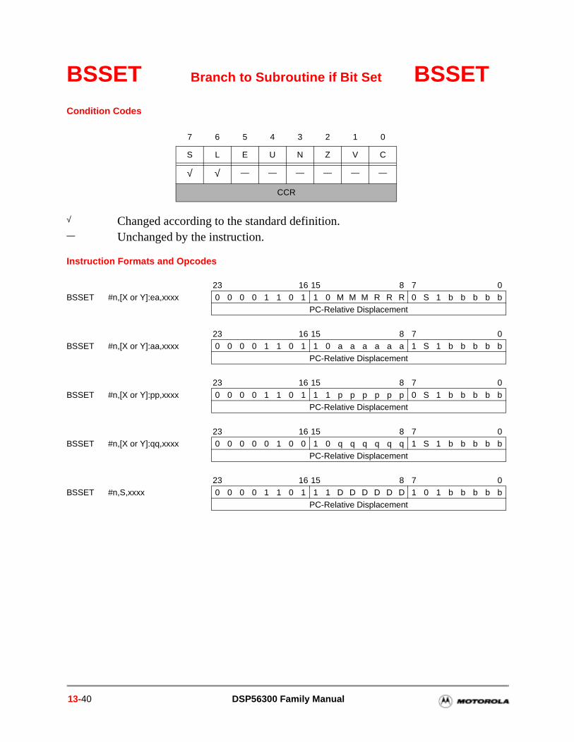
BSSET Branch to Subroutine if Bit Set BSSETCondition Codes
Instruction Formats and Opcodes
7 6 5 4 3 2 1 0
S L E U N Z V C
√ √ — — — — — —
CCR
√ Changed according to the standard definition.— Unchanged by the instruction.
23 16 15 8 7 0BSSET #n,[X or Y]:ea,xxxx 0 0 0 0 1 1 0 1 1 0 M M M R R R 0 S 1 b b b b b
PC-Relative Displacement
23 16 15 8 7 0BSSET #n,[X or Y]:aa,xxxx 0 0 0 0 1 1 0 1 1 0 a a a a a a 1 S 1 b b b b b
PC-Relative Displacement
23 16 15 8 7 0
BSSET #n,[X or Y]:pp,xxxx 0 0 0 0 1 1 0 1 1 1 p p p p p p 0 S 1 b b b b bPC-Relative Displacement
23 16 15 8 7 0BSSET #n,[X or Y]:qq,xxxx 0 0 0 0 0 1 0 0 1 0 q q q q q q 1 S 1 b b b b b
PC-Relative Displacement
23 16 15 8 7 0BSSET #n,S,xxxx 0 0 0 0 1 1 0 1 1 1 D D D D D D 1 0 1 b b b b b
PC-Relative Displacement
13-40 DSP56300 Family Manual
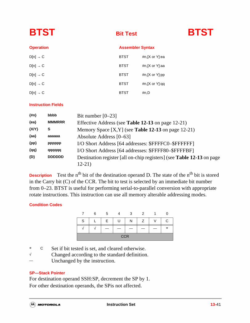
te
BTST Bit Test BTST
Instruction Fields
Description Test the nth bit of the destination operand D. The state of the nth bit is stored in the Carry bit (C) of the CCR. The bit to test is selected by an immediate bit number from 0–23. BTST is useful for performing serial-to-parallel conversion with appropriarotate instructions. This instruction can use all memory alterable addressing modes.
Condition Codes
Operation Assembler Syntax
D[n] → C BTST #n,[X or Y]:ea
D[n] → C BTST #n,[X or Y]:aa
D[n] → C BTST #n,[X or Y]:pp
D[n] → C BTST #n,[X or Y]:qq
D[n] → C BTST #n,D
#n bbbb Bit number [0–23]ea MMMRRR Effective Address (see Table 12-13 on page 12-21)X/Y S Memory Space [X,Y] (see Table 12-13 on page 12-21)aa aaaaaa Absolute Address [0–63]pp pppppp I/O Short Address [64 addresses: $FFFFC0–$FFFFFF]qq qqqqqq I/O Short Address [64 addresses: $FFFF80–$FFFFBF]D DDDDDD Destination register [all on-chip registers] (see Table 12-13 on page
12-21)
7 6 5 4 3 2 1 0
S L E U N Z V C
√ √ — — — — — *
CCR
* C Set if bit tested is set, and cleared otherwise.√ Changed according to the standard definition.— Unchanged by the instruction.
SP—Stack Pointer
For destination operand SSH:SP, decrement the SP by 1.For other destination operands, the SPis not affected.
Instruction Set 13-41
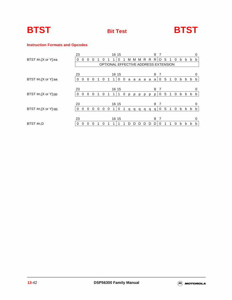
BTST Bit Test BTSTInstruction Formats and Opcodes
23 16 15 8 7 0
BTST #n,[X or Y]:ea 0 0 0 0 1 0 1 1 0 1 M M M R R R O S 1 0 b b b bOPTIONAL EFFECTIVE ADDRESS EXTENSION
23 16 15 8 7 0BTST #n,[X or Y]:aa 0 0 0 0 1 0 1 1 0 0 a a a a a a 0 S 1 0 b b b b
23 16 15 8 7 0BTST #n,[X or Y]:pp 0 0 0 0 1 0 1 1 1 0 p p p p p p 0 S 1 0 b b b b
23 16 15 8 7 0BTST #n,[X or Y]:qq 0 0 0 0 0 0 0 1 0 1 q q q q q q 0 S 1 0 b b b b
23 16 15 8 7 0BTST #n,D 0 0 0 0 1 0 1 1 1 1 D D D D D D 0 1 1 0 b b b b
13-42 DSP56300 Family Manual
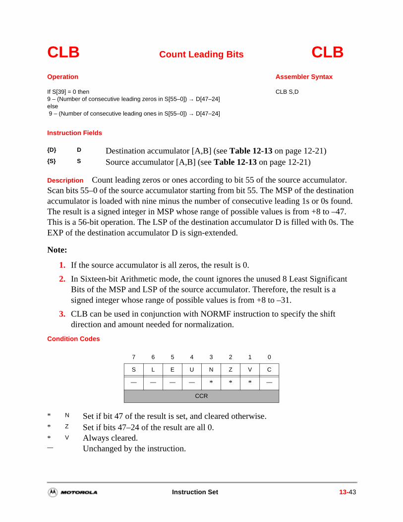
tion ound. 47.
The
nt
CLB Count Leading Bits CLB
Instruction Fields
Description Count leading zeros or ones according to bit 55 of the source accumulator. Scan bits 55–0 of the source accumulator starting from bit 55. The MSP of the destinaaccumulator is loaded with nine minus the number of consecutive leading 1s or 0s fThe result is a signed integer in MSP whose range of possible values is from +8 to –This is a 56-bit operation. The LSP of the destination accumulator D is filled with 0s.EXP of the destination accumulator D is sign-extended.
Note:
1. If the source accumulator is all zeros, the result is 0.
2. In Sixteen-bit Arithmetic mode, the count ignores the unused 8 Least SignificaBits of the MSP and LSP of the source accumulator. Therefore, the result is asigned integer whose range of possible values is from +8 to –31.
3. CLB can be used in conjunction with NORMF instruction to specify the shift direction and amount needed for normalization.
Condition Codes
Operation Assembler Syntax
If S[39] = 0 then 9 – (Number of consecutive leading zeros in S[55–0]) → D[47–24]
CLB S,D
else 9 – (Number of consecutive leading ones in S[55–0]) → D[47–24]
D D Destination accumulator [A,B] (see Table 12-13 on page 12-21)S S Source accumulator [A,B] (see Table 12-13 on page 12-21)
7 6 5 4 3 2 1 0
S L E U N Z V C
— — — — * * * —
CCR
* N Set if bit 47 of the result is set, and cleared otherwise.* Z Set if bits 47–24 of the result are all 0.* V Always cleared.— Unchanged by the instruction.
Instruction Set 13-43
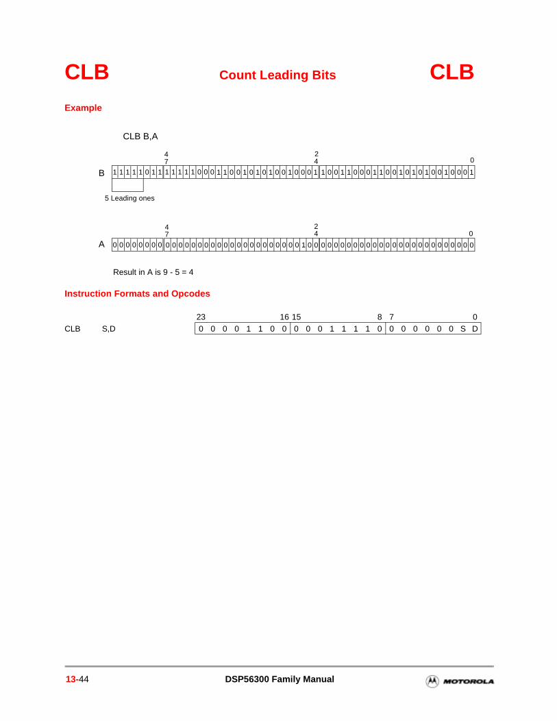
CLB Count Leading Bits CLBExample
Instruction Formats and Opcodes
23 16 15 8 7 0CLB S,D 0 0 0 0 1 1 0 0 0 0 0 1 1 1 1 0 0 0 0 0 0 0 S D
CLB B,A
5 Leading ones
Result in A is 9 - 5 = 4
0 0 0 0 0 0 0 0 0 0 0 0 0 0 0 0 0 0 0 0 0 1 0 0
447
2
1 1 1 1 1 0 0 0 1 1 0 0 1 0 1 0 1 0 0 1 0 0 0 1
447
2
1 0 0 1 1 0 0 0 1 1 0 0 1 0 1 0 1 0 0 1 0 0 0 1
0
B
A
1 1 1 1 1 0 1 1
0 0 0 0 0 0 0 0 0 0 0 0 0 0 0 0 0 0 0 0 0 0 0 0
0
0 0 0 0 0 0 0 0
13-44 DSP56300 Family Manual
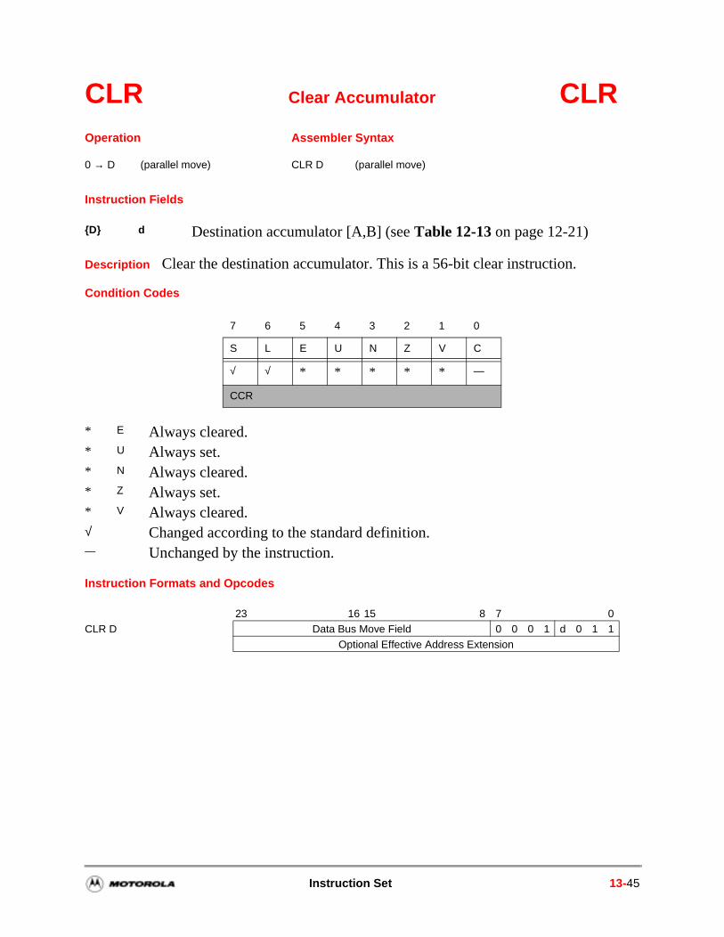
CLR Clear Accumulator CLR
Instruction Fields
Description Clear the destination accumulator. This is a 56-bit clear instruction.
Condition Codes
Instruction Formats and Opcodes
Operation Assembler Syntax
0 → D (parallel move) CLR D (parallel move)
D d Destination accumulator [A,B] (see Table 12-13 on page 12-21)
7 6 5 4 3 2 1 0
S L E U N Z V C
√ √ * * * * * —
CCR
* E Always cleared.* U Always set.* N Always cleared.* Z Always set.* V Always cleared.√ Changed according to the standard definition.— Unchanged by the instruction.
23 16 15 8 7 0CLR D Data Bus Move Field 0 0 0 1 d 0 1 1
Optional Effective Address Extension
Instruction Set 13-45
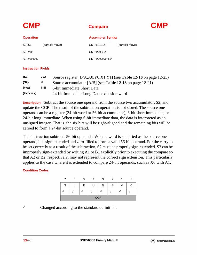
CMP Compare CMP
Instruction Fields
Description Subtract the source one operand from the source two accumulator, S2, and update the CCR. The result of the subtraction operation is not stored. The source one operand can be a register (24-bit word or 56-bit accumulator), 6-bit short immediate, or 24-bit long immediate. When using 6-bit immediate data, the data is interpreted as an unsigned integer. That is, the six bits will be right-aligned and the remaining bits will be zeroed to form a 24-bit source operand.
This instruction subtracts 56-bit operands. When a word is specified as the source one operand, it is sign-extended and zero-filled to form a valid 56-bit operand. For the carry to be set correctly as a result of the subtraction, S2 must be properly sign-extended. S2 can be improperly sign-extended by writing A1 or B1 explicitly prior to executing the compare so that A2 or B2, respectively, may not represent the correct sign extension. This particularly applies to the case where it is extended to compare 24-bit operands, such as X0 with A1.
Condition Codes
Operation Assembler Syntax
S2–S1 (parallel move) CMP S1, S2 (parallel move)
S2–#xx CMP #xx, S2
S2–#xxxxxx CMP #xxxxxx, S2
S1 JJJ Source register [B/A,X0,Y0,X1,Y1] (see Table 12-16 on page 12-23)S2 d Source accumulator [A/B] (see Table 12-13 on page 12-21)#xx iiiiii 6-bit Immediate Short Data #xxxxxx 24-bit Immediate Long Data extension word
7 6 5 4 3 2 1 0
S L E U N Z V C
√ √ √ √ √ √ √ √
CCR
√ Changed according to the standard definition.
13-46 DSP56300 Family Manual
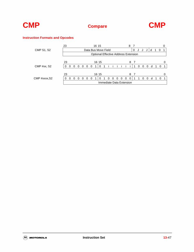
CMP Compare CMPInstruction Formats and Opcodes
23 16 15 8 7 0
CMP S1, S2 Data Bus Move Field 0 J J J d 1 0 1Optional Effective Address Extension
23 16 15 8 7 0
CMP #xx, S2 0 0 0 0 0 0 0 1 0 1 i i i i i i 1 0 0 0 d 1 0 1
23 16 15 8 7 0CMP #xxxx,S2 0 0 0 0 0 0 0 1 0 1 0 0 0 0 0 0 1 1 0 0 d 1 0 1
Immediate Data Extension
Instruction Set 13-47
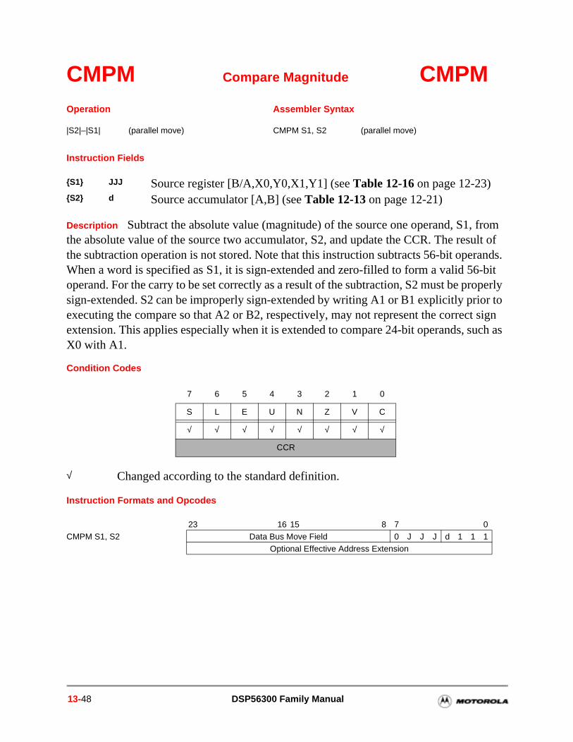
CMPM Compare Magnitude CMPM
Instruction Fields
Description Subtract the absolute value (magnitude) of the source one operand, S1, from the absolute value of the source two accumulator, S2, and update the CCR. The result of the subtraction operation is not stored. Note that this instruction subtracts 56-bit operands. When a word is specified as S1, it is sign-extended and zero-filled to form a valid 56-bit operand. For the carry to be set correctly as a result of the subtraction, S2 must be properly sign-extended. S2 can be improperly sign-extended by writing A1 or B1 explicitly prior to executing the compare so that A2 or B2, respectively, may not represent the correct sign extension. This applies especially when it is extended to compare 24-bit operands, such as X0 with A1.
Condition Codes
Instruction Formats and Opcodes
Operation Assembler Syntax
|S2|–|S1| (parallel move) CMPM S1, S2 (parallel move)
S1 JJJ Source register [B/A,X0,Y0,X1,Y1] (see Table 12-16 on page 12-23)S2 d Source accumulator [A,B] (see Table 12-13 on page 12-21)
7 6 5 4 3 2 1 0
S L E U N Z V C
√ √ √ √ √ √ √ √
CCR
√ Changed according to the standard definition.
23 16 15 8 7 0CMPM S1, S2 Data Bus Move Field 0 J J J d 1 1 1
Optional Effective Address Extension
13-48 DSP56300 Family Manual
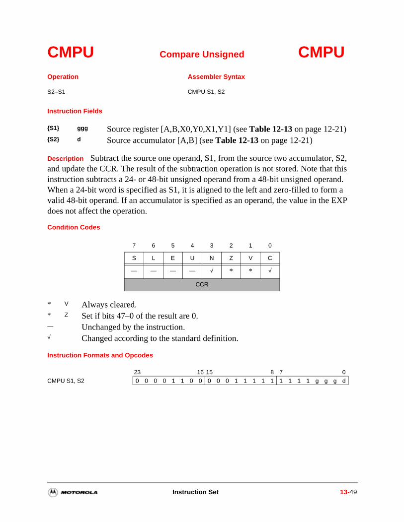
CMPU Compare Unsigned CMPU
Instruction Fields
Description Subtract the source one operand, S1, from the source two accumulator, S2, and update the CCR. The result of the subtraction operation is not stored. Note that this instruction subtracts a 24- or 48-bit unsigned operand from a 48-bit unsigned operand. When a 24-bit word is specified as S1, it is aligned to the left and zero-filled to form a valid 48-bit operand. If an accumulator is specified as an operand, the value in the EXP does not affect the operation.
Condition Codes
Instruction Formats and Opcodes
Operation Assembler Syntax
S2–S1 CMPU S1, S2
S1 ggg Source register [A,B,X0,Y0,X1,Y1] (see Table 12-13 on page 12-21)S2 d Source accumulator [A,B] (see Table 12-13 on page 12-21)
7 6 5 4 3 2 1 0
S L E U N Z V C
— — — — √ * * √
CCR
* V Always cleared.* Z Set if bits 47–0 of the result are 0.— Unchanged by the instruction.√ Changed according to the standard definition.
23 16 15 8 7 0
CMPU S1, S2 0 0 0 0 1 1 0 0 0 0 0 1 1 1 1 1 1 1 1 1 g g g d
Instruction Set 13-49
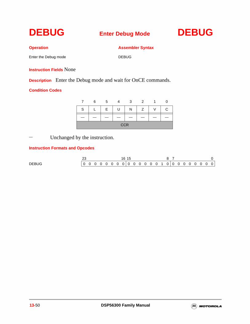
DEBUG Enter Debug Mode DEBUG
Instruction Fields None
Description Enter the Debug mode and wait for OnCE commands.
Condition Codes
Instruction Formats and Opcodes
Operation Assembler Syntax
Enter the Debug mode DEBUG
7 6 5 4 3 2 1 0
S L E U N Z V C
— — — — — — — —
CCR
— Unchanged by the instruction.
23 16 15 8 7 0
DEBUG 0 0 0 0 0 0 0 0 0 0 0 0 0 0 1 0 0 0 0 0 0 0 0 0
13-50 DSP56300 Family Manual
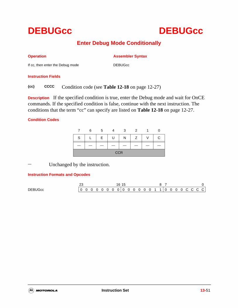
DEBUGcc DEBUGccEnter Debug Mode Conditionally
Instruction Fields
Description If the specified condition is true, enter the Debug mode and wait for OnCE commands. If the specified condition is false, continue with the next instruction. The conditions that the term “cc” can specify are listed on Table 12-18 on page 12-27.
Condition Codes
Instruction Formats and Opcodes
Operation Assembler Syntax
If cc, then enter the Debug mode DEBUGcc
cc CCCC Condition code (see Table 12-18 on page 12-27)
7 6 5 4 3 2 1 0
S L E U N Z V C
— — — — — — — —
CCR
— Unchanged by the instruction.
23 16 15 8 7 0
DEBUGcc 0 0 0 0 0 0 0 0 0 0 0 0 0 0 1 1 0 0 0 0 C C C C
Instruction Set 13-51
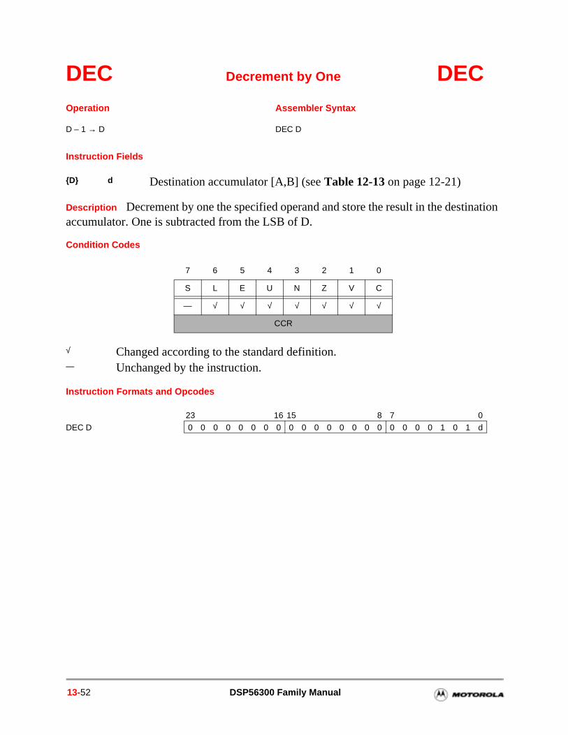
DEC Decrement by One DEC
Instruction Fields
Description Decrement by one the specified operand and store the result in the destination accumulator. One is subtracted from the LSB of D.
Condition Codes
Instruction Formats and Opcodes
Operation Assembler Syntax
D – 1 → D DEC D
D d Destination accumulator [A,B] (see Table 12-13 on page 12-21)
7 6 5 4 3 2 1 0
S L E U N Z V C
— √ √ √ √ √ √ √
CCR
√ Changed according to the standard definition.— Unchanged by the instruction.
23 16 15 8 7 0
DEC D 0 0 0 0 0 0 0 0 0 0 0 0 0 0 0 0 0 0 0 0 1 0 1 d
13-52 DSP56300 Family Manual
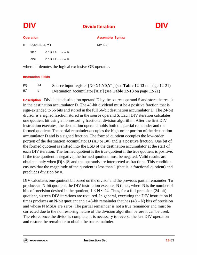
cision st be ed.
tion
DIV Divide Iteration DIV
Instruction Fields
Description Divide the destination operand D by the source operand S and store the result in the destination accumulator D. The 48-bit dividend must be a positive fraction that is sign-extended to 56 bits and stored in the full 56-bit destination accumulator D. The 24-bit divisor is a signed fraction stored in the source operand S. Each DIV iteration calculates one quotient bit using a nonrestoring fractional division algorithm. After the first DIV instruction executes, the destination operand holds both the partial remainder and the formed quotient. The partial remainder occupies the high-order portion of the destination accumulator D and is a signed fraction. The formed quotient occupies the low-order portion of the destination accumulator D (A0 or B0) and is a positive fraction. One bit of the formed quotient is shifted into the LSB of the destination accumulator at the start of each DIV iteration. The formed quotient is the true quotient if the true quotient is positive. If the true quotient is negative, the formed quotient must be negated. Valid results are obtained only when |D| < |S| and the operands are interpreted as fractions. This condition ensures that the magnitude of the quotient is less than 1 (that is, a fractional quotient) and precludes division by 0.
DIV calculates one quotient bit based on the divisor and the previous partial remainder. To produce an N-bit quotient, the DIV instruction executes N times, where N is the number of bits of precision desired in the quotient, 1 ≤ N ≤ 24. Thus, for a full-precision (24-bit) quotient, sixteen DIV iterations are required. In general, executing the DIV instruction N times produces an N-bit quotient and a 48-bit remainder that has (48 – N) bits of preand whose N MSBs are zeros. The partial remainder is not a true remainder and mucorrected due to the nonrestoring nature of the division algorithm before it can be usTherefore, once the divide is complete, it is necessary to reverse the last DIV operaand restore the remainder to obtain the true remainder.
Operation Assembler Syntax
IF D[39]⊕S[15] = 1 DIV S,D
then 2 ∗ D + C + S → D
else 2 ∗ D + C – S → D
where ⊕ denotes the logical exclusive OR operator.
S JJ Source input register [X0,X1,Y0,Y1] (see Table 12-13 on page 12-21)D d Destination accumulator [A,B] (see Table 12-13 on page 12-21)
Instruction Set 13-53
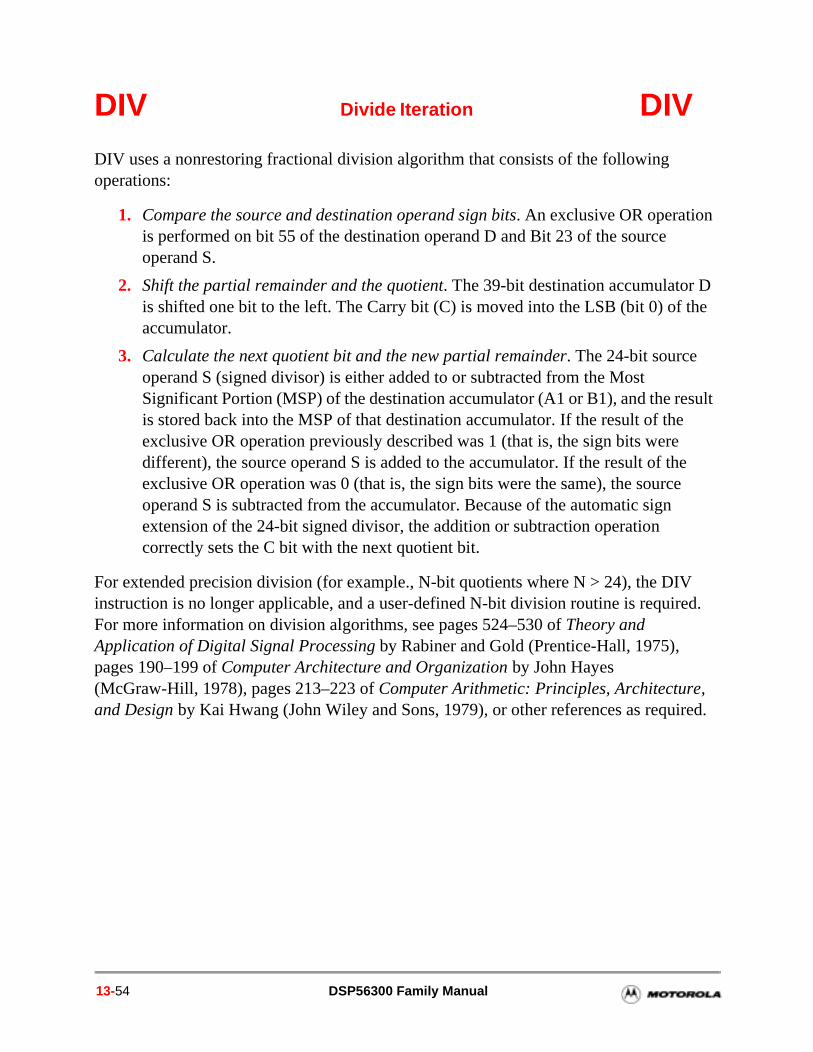
ired.
DIV Divide Iteration DIV
DIV uses a nonrestoring fractional division algorithm that consists of the following operations:
1. Compare the source and destination operand sign bits. An exclusive OR operation is performed on bit 55 of the destination operand D and Bit 23 of the source operand S.
2. Shift the partial remainder and the quotient. The 39-bit destination accumulator D is shifted one bit to the left. The Carry bit (C) is moved into the LSB (bit 0) of the accumulator.
3. Calculate the next quotient bit and the new partial remainder. The 24-bit source operand S (signed divisor) is either added to or subtracted from the Most Significant Portion (MSP) of the destination accumulator (A1 or B1), and the result is stored back into the MSP of that destination accumulator. If the result of the exclusive OR operation previously described was 1 (that is, the sign bits were different), the source operand S is added to the accumulator. If the result of the exclusive OR operation was 0 (that is, the sign bits were the same), the source operand S is subtracted from the accumulator. Because of the automatic sign extension of the 24-bit signed divisor, the addition or subtraction operation correctly sets the C bit with the next quotient bit.
For extended precision division (for example., N-bit quotients where N > 24), the DIV instruction is no longer applicable, and a user-defined N-bit division routine is required. For more information on division algorithms, see pages 524–530 of Theory and Application of Digital Signal Processing by Rabiner and Gold (Prentice-Hall, 1975), pages 190–199 of Computer Architecture and Organization by John Hayes (McGraw-Hill, 1978), pages 213–223 of Computer Arithmetic: Principles, Architecture, and Design by Kai Hwang (John Wiley and Sons, 1979), or other references as requ
13-54 DSP56300 Family Manual
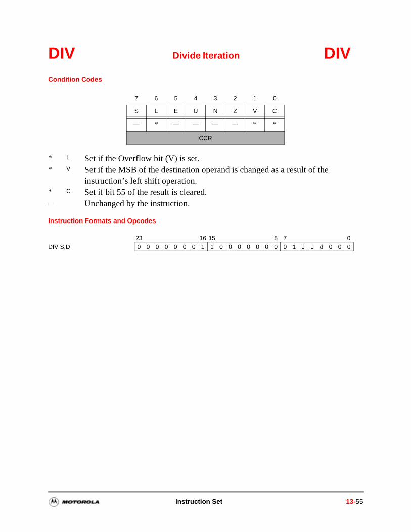
DIV Divide Iteration DIVCondition Codes
Instruction Formats and Opcodes
7 6 5 4 3 2 1 0
S L E U N Z V C
— * — — — — * *
CCR
* L Set if the Overflow bit (V) is set.* V Set if the MSB of the destination operand is changed as a result of the
instruction’s left shift operation.* C Set if bit 55 of the result is cleared.— Unchanged by the instruction.
23 16 15 8 7 0
DIV S,D 0 0 0 0 0 0 0 1 1 0 0 0 0 0 0 0 0 1 J J d 0 0 0
Instruction Set 13-55
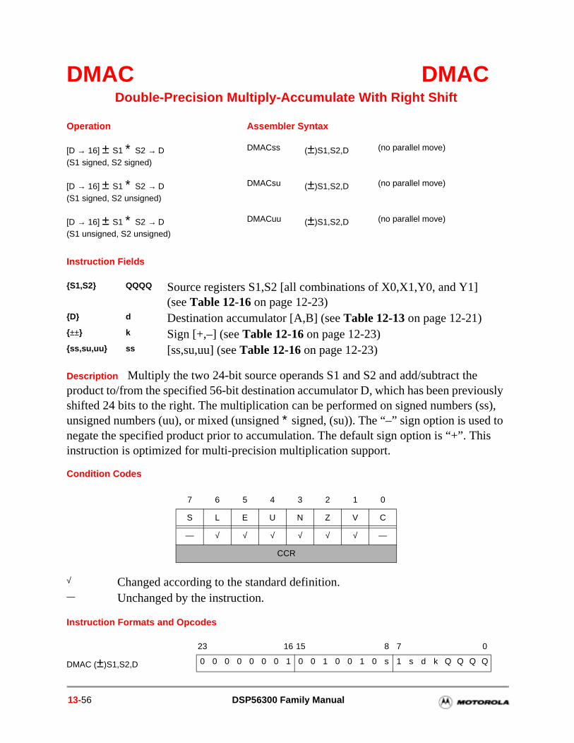
o is
DMAC DMACDouble-Precision Multiply-Accumulate With Right Shift
Instruction Fields
Description Multiply the two 24-bit source operands S1 and S2 and add/subtract the product to/from the specified 56-bit destination accumulator D, which has been previously shifted 24 bits to the right. The multiplication can be performed on signed numbers (ss), unsigned numbers (uu), or mixed (unsigned ∗ signed, (su)). The “–” sign option is used tnegate the specified product prior to accumulation. The default sign option is “+”. Thinstruction is optimized for multi-precision multiplication support.
Condition Codes
Instruction Formats and Opcodes
Operation Assembler Syntax
[D → 16] ± S1 ∗ S2 → D (S1 signed, S2 signed)
DMACss (±)S1,S2,D (no parallel move)
[D → 16] ± S1 ∗ S2 → D (S1 signed, S2 unsigned)
DMACsu (±)S1,S2,D (no parallel move)
[D → 16] ± S1 ∗ S2 → D (S1 unsigned, S2 unsigned)
DMACuu (±)S1,S2,D (no parallel move)
S1,S2 QQQQ Source registers S1,S2 [all combinations of X0,X1,Y0, and Y1] (see Table 12-16 on page 12-23)
D d Destination accumulator [A,B] (see Table 12-13 on page 12-21)±± k Sign [+,–] (see Table 12-16 on page 12-23)ss,su,uu ss [ss,su,uu] (see Table 12-16 on page 12-23)
7 6 5 4 3 2 1 0
S L E U N Z V C
— √ √ √ √ √ √ —
CCR
√ Changed according to the standard definition.— Unchanged by the instruction.
23 16 15 8 7 0
DMAC (±)S1,S2,D 0 0 0 0 0 0 0 1 0 0 1 0 0 1 0 s 1 s d k Q Q Q Q
13-56 DSP56300 Family Manual
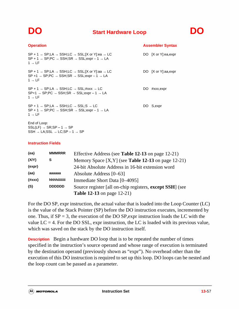
ated e d and
DO Start Hardware Loop DO
Instruction Fields
For the DO SP, expr instruction, the actual value that is loaded into the Loop Counter (LC) is the value of the Stack Pointer (SP) before the DO instruction executes, incremented by one. Thus, if SP = 3, the execution of the DO SP,expr instruction loads the LC with the value LC = 4. For the DO SSL, expr instruction, the LC is loaded with its previous value, which was saved on the stack by the DO instruction itself.
Description Begin a hardware DO loop that is to be repeated the number of times specified in the instruction’s source operand and whose range of execution is terminby the destination operand (previously shown as “expr”). No overhead other than thexecution of this DO instruction is required to set up this loop. DO loops can be nestethe loop count can be passed as a parameter.
Operation Assembler Syntax
SP + 1 → SP;LA → SSH;LC → SSL;[X or Y]:ea → LC DO [X or Y]:ea,exprSP + 1 → SP;PC → SSH;SR → SSL;expr – 1 → LA1 → LF
SP + 1 → SP;LA → SSH;LC → SSL;[X or Y]:aa → LC DO [X or Y]:aa,exprSP +1 → SP;PC → SSH;SR → SSL;expr – 1 → LA1 → LF
SP + 1 → SP;LA → SSH;LC → SSL;#xxx → LC DO #xxx,exprSP+1 → SP;PC → SSH;SR → SSL;expr – 1 → LA1 → LF
SP + 1 → SP;LA → SSH;LC → SSL;S → LC DO S,exprSP + 1 → SP;PC → SSH;SR → SSL;expr – 1 → LA1 → LF
End of Loop:SSL(LF) → SR;SP – 1 → SPSSH → LA;SSL → LC;SP – 1 → SP
ea MMMRRR Effective Address (see Table 12-13 on page 12-21)X/Y S Memory Space [X,Y] (see Table 12-13 on page 12-21)expr 24-bit Absolute Address in 16-bit extension wordaa aaaaaa Absolute Address [0–63]#xxx hhhhiiiiiiii Immediate Short Data [0–4095]S DDDDDD Source register [all on-chip registers, except SSH] (see
Table 12-13 on page 12-21)
Instruction Set 13-57
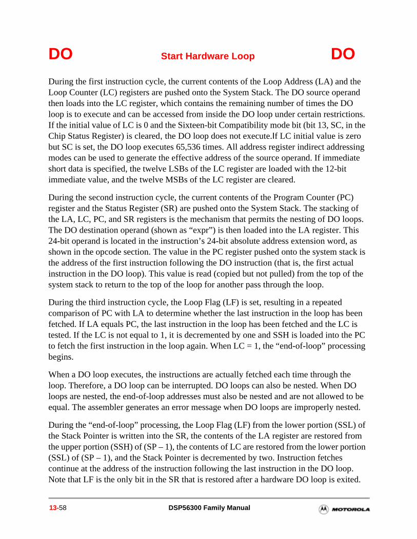
his , as tack is l the
een is
he PC sing
e DO d to be ested.
) of from ortion
. ted.
DO Start Hardware Loop DO
During the first instruction cycle, the current contents of the Loop Address (LA) and the Loop Counter (LC) registers are pushed onto the System Stack. The DO source operand then loads into the LC register, which contains the remaining number of times the DO loop is to execute and can be accessed from inside the DO loop under certain restrictions. If the initial value of LC is 0 and the Sixteen-bit Compatibility mode bit (bit 13, SC, in the Chip Status Register) is cleared, the DO loop does not execute.If LC initial value is zero but SC is set, the DO loop executes 65,536 times. All address register indirect addressing modes can be used to generate the effective address of the source operand. If immediate short data is specified, the twelve LSBs of the LC register are loaded with the 12-bit immediate value, and the twelve MSBs of the LC register are cleared.
During the second instruction cycle, the current contents of the Program Counter (PC) register and the Status Register (SR) are pushed onto the System Stack. The stacking of the LA, LC, PC, and SR registers is the mechanism that permits the nesting of DO loops. The DO destination operand (shown as “expr”) is then loaded into the LA register. T24-bit operand is located in the instruction’s 24-bit absolute address extension wordshown in the opcode section. The value in the PC register pushed onto the system sthe address of the first instruction following the DO instruction (that is, the first actuainstruction in the DO loop). This value is read (copied but not pulled) from the top ofsystem stack to return to the top of the loop for another pass through the loop.
During the third instruction cycle, the Loop Flag (LF) is set, resulting in a repeated comparison of PC with LA to determine whether the last instruction in the loop has bfetched. If LA equals PC, the last instruction in the loop has been fetched and the LCtested. If the LC is not equal to 1, it is decremented by one and SSH is loaded into tto fetch the first instruction in the loop again. When LC = 1, the “end-of-loop” procesbegins.
When a DO loop executes, the instructions are actually fetched each time through thloop. Therefore, a DO loop can be interrupted. DO loops can also be nested. When loops are nested, the end-of-loop addresses must also be nested and are not alloweequal. The assembler generates an error message when DO loops are improperly n
During the “end-of-loop” processing, the Loop Flag (LF) from the lower portion (SSLthe Stack Pointer is written into the SR, the contents of the LA register are restored the upper portion (SSH) of (SP – 1), the contents of LC are restored from the lower p(SSL) of (SP – 1), and the Stack Pointer is decremented by two. Instruction fetches continue at the address of the instruction following the last instruction in the DO loopNote that LF is the only bit in the SR that is restored after a hardware DO loop is exi
13-58 DSP56300 Family Manual
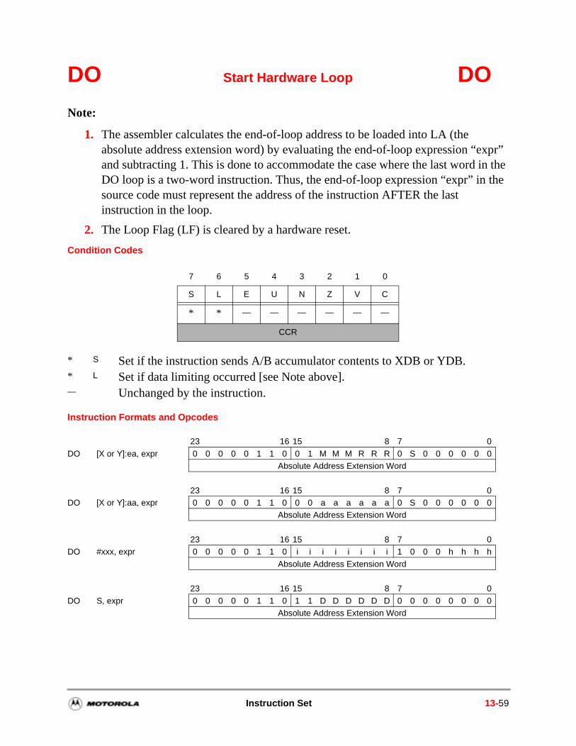
xpr” in the the
DO Start Hardware Loop DO
Note:
1. The assembler calculates the end-of-loop address to be loaded into LA (the absolute address extension word) by evaluating the end-of-loop expression “eand subtracting 1. This is done to accommodate the case where the last wordDO loop is a two-word instruction. Thus, the end-of-loop expression “expr” in source code must represent the address of the instruction AFTER the last instruction in the loop.
2. The Loop Flag (LF) is cleared by a hardware reset.
Condition Codes
Instruction Formats and Opcodes
7 6 5 4 3 2 1 0
S L E U N Z V C
* * — — — — — —
CCR
* S Set if the instruction sends A/B accumulator contents to XDB or YDB.* L Set if data limiting occurred [see Note above].— Unchanged by the instruction.
23 16 15 8 7 0
DO [X or Y]:ea, expr 0 0 0 0 0 1 1 0 0 1 M M M R R R 0 S 0 0 0 0 0 0Absolute Address Extension Word
23 16 15 8 7 0DO [X or Y]:aa, expr 0 0 0 0 0 1 1 0 0 0 a a a a a a 0 S 0 0 0 0 0 0
Absolute Address Extension Word
23 16 15 8 7 0DO #xxx, expr 0 0 0 0 0 1 1 0 i i i i i i i i 1 0 0 0 h h h h
Absolute Address Extension Word
23 16 15 8 7 0
DO S, expr 0 0 0 0 0 1 1 0 1 1 D D D D D D 0 0 0 0 0 0 0 0Absolute Address Extension Word
Instruction Set 13-59
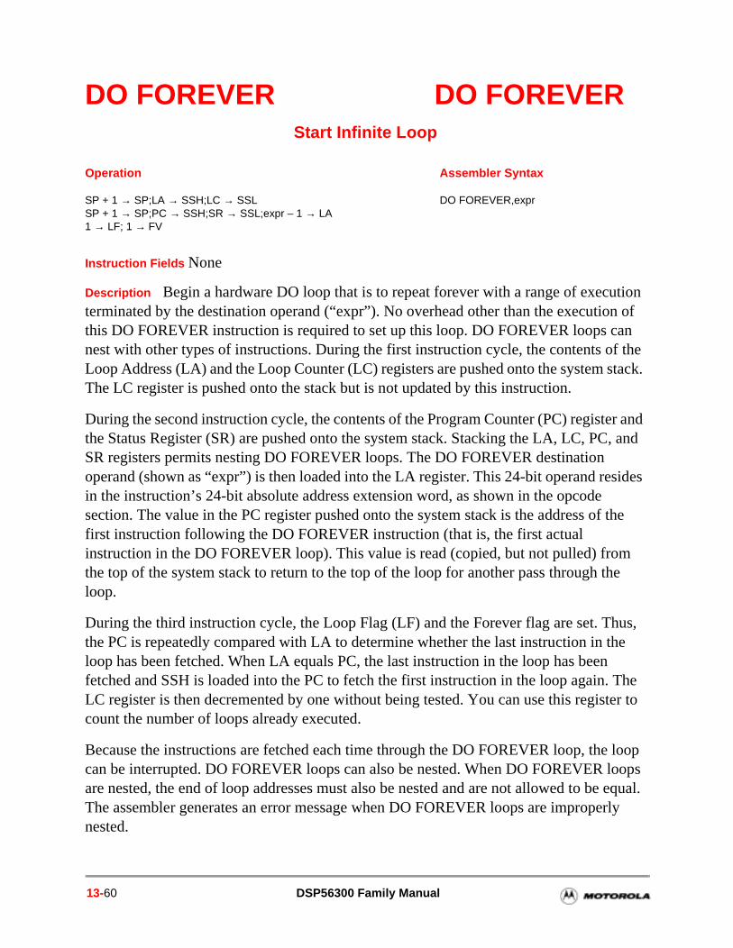
n of an f the stack.
er and , and
sides
f the
m he
us, he
The ter to
loop loops e equal. rly
DO FOREVER DO FOREVERStart Infinite Loop
Instruction Fields None
Description Begin a hardware DO loop that is to repeat forever with a range of execution terminated by the destination operand (“expr”). No overhead other than the executiothis DO FOREVER instruction is required to set up this loop. DO FOREVER loops cnest with other types of instructions. During the first instruction cycle, the contents oLoop Address (LA) and the Loop Counter (LC) registers are pushed onto the system The LC register is pushed onto the stack but is not updated by this instruction.
During the second instruction cycle, the contents of the Program Counter (PC) registthe Status Register (SR) are pushed onto the system stack. Stacking the LA, LC, PCSR registers permits nesting DO FOREVER loops. The DO FOREVER destination operand (shown as “expr”) is then loaded into the LA register. This 24-bit operand rein the instruction’s 24-bit absolute address extension word, as shown in the opcode section. The value in the PC register pushed onto the system stack is the address ofirst instruction following the DO FOREVER instruction (that is, the first actual instruction in the DO FOREVER loop). This value is read (copied, but not pulled) frothe top of the system stack to return to the top of the loop for another pass through tloop.
During the third instruction cycle, the Loop Flag (LF) and the Forever flag are set. Ththe PC is repeatedly compared with LA to determine whether the last instruction in tloop has been fetched. When LA equals PC, the last instruction in the loop has beenfetched and SSH is loaded into the PC to fetch the first instruction in the loop again.LC register is then decremented by one without being tested. You can use this regiscount the number of loops already executed.
Because the instructions are fetched each time through the DO FOREVER loop, thecan be interrupted. DO FOREVER loops can also be nested. When DO FOREVER are nested, the end of loop addresses must also be nested and are not allowed to bThe assembler generates an error message when DO FOREVER loops are impropenested.
Operation Assembler Syntax
SP + 1 → SP;LA → SSH;LC → SSL DO FOREVER,exprSP + 1 → SP;PC → SSH;SR → SSL;expr – 1 → LA1 → LF; 1 → FV
13-60 DSP56300 Family Manual
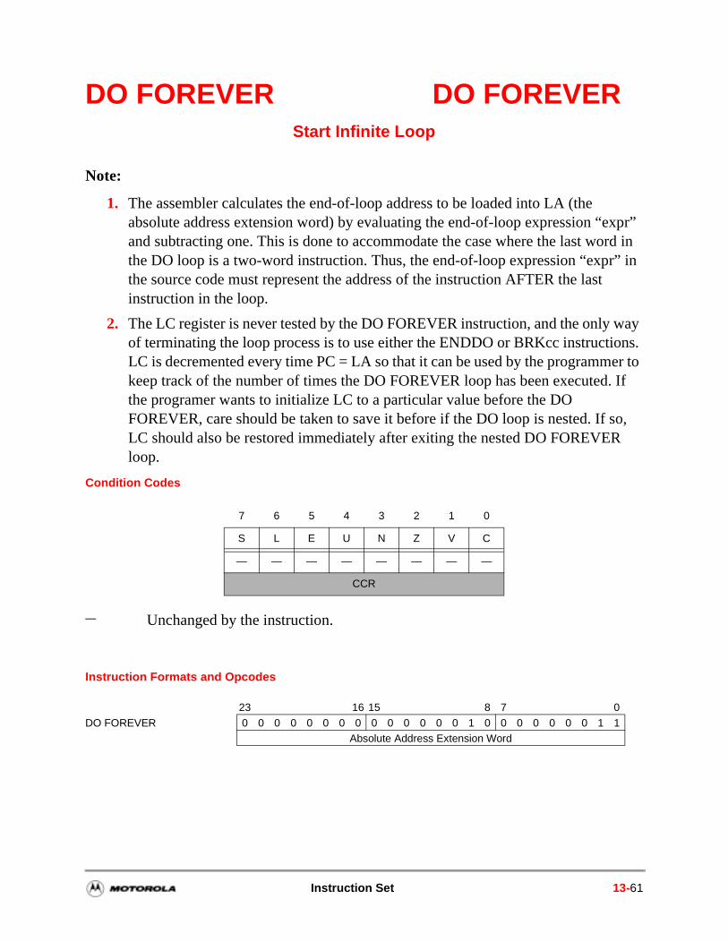
xpr” rd in
” in
way ons. er to . If
so, R
DO FOREVER DO FOREVERStart Infinite Loop
Note:
1. The assembler calculates the end-of-loop address to be loaded into LA (the absolute address extension word) by evaluating the end-of-loop expression “eand subtracting one. This is done to accommodate the case where the last wothe DO loop is a two-word instruction. Thus, the end-of-loop expression “exprthe source code must represent the address of the instruction AFTER the lastinstruction in the loop.
2. The LC register is never tested by the DO FOREVER instruction, and the onlyof terminating the loop process is to use either the ENDDO or BRKcc instructiLC is decremented every time PC = LA so that it can be used by the programmkeep track of the number of times the DO FOREVER loop has been executedthe programer wants to initialize LC to a particular value before the DO FOREVER, care should be taken to save it before if the DO loop is nested. If LC should also be restored immediately after exiting the nested DO FOREVEloop.
Condition Codes
Instruction Formats and Opcodes
7 6 5 4 3 2 1 0
S L E U N Z V C
— — — — — — — —
CCR
— Unchanged by the instruction.
23 16 15 8 7 0
DO FOREVER 0 0 0 0 0 0 0 0 0 0 0 0 0 0 1 0 0 0 0 0 0 0 1 1Absolute Address Extension Word
Instruction Set 13-61
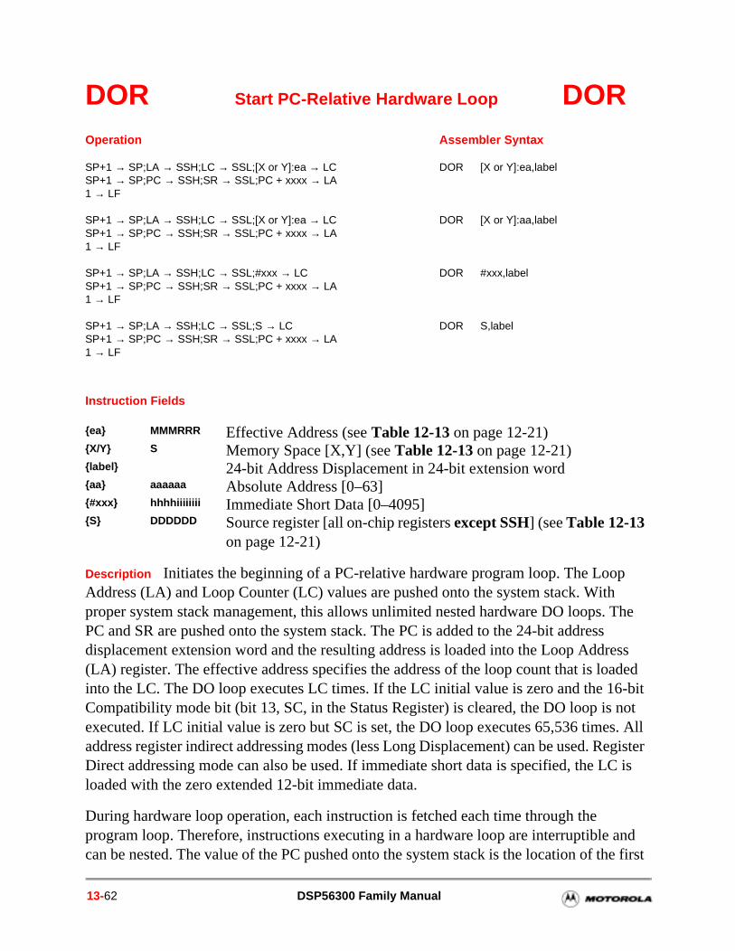
DOR Start PC-Relative Hardware Loop DOR
Instruction Fields
Description Initiates the beginning of a PC-relative hardware program loop. The Loop Address (LA) and Loop Counter (LC) values are pushed onto the system stack. With proper system stack management, this allows unlimited nested hardware DO loops. The PC and SR are pushed onto the system stack. The PC is added to the 24-bit address displacement extension word and the resulting address is loaded into the Loop Address (LA) register. The effective address specifies the address of the loop count that is loaded into the LC. The DO loop executes LC times. If the LC initial value is zero and the 16-bit Compatibility mode bit (bit 13, SC, in the Status Register) is cleared, the DO loop is not executed. If LC initial value is zero but SC is set, the DO loop executes 65,536 times. All address register indirect addressing modes (less Long Displacement) can be used. Register Direct addressing mode can also be used. If immediate short data is specified, the LC is loaded with the zero extended 12-bit immediate data.
During hardware loop operation, each instruction is fetched each time through the program loop. Therefore, instructions executing in a hardware loop are interruptible and can be nested. The value of the PC pushed onto the system stack is the location of the first
Operation Assembler Syntax
SP+1 → SP;LA → SSH;LC → SSL;[X or Y]:ea → LC DOR [X or Y]:ea,labelSP+1 → SP;PC → SSH;SR → SSL;PC + xxxx → LA1 → LF
SP+1 → SP;LA → SSH;LC → SSL;[X or Y]:ea → LC DOR [X or Y]:aa,labelSP+1 → SP;PC → SSH;SR → SSL;PC + xxxx → LA1 → LF
SP+1 → SP;LA → SSH;LC → SSL;#xxx → LC DOR #xxx,labelSP+1 → SP;PC → SSH;SR → SSL;PC + xxxx → LA1 → LF
SP+1 → SP;LA → SSH;LC → SSL;S → LC DOR S,labelSP+1 → SP;PC → SSH;SR → SSL;PC + xxxx → LA1 → LF
ea MMMRRR Effective Address (see Table 12-13 on page 12-21)X/Y S Memory Space [X,Y] (see Table 12-13 on page 12-21)label 24-bit Address Displacement in 24-bit extension wordaa aaaaaa Absolute Address [0–63]#xxx hhhhiiiiiiii Immediate Short Data [0–4095]S DDDDDD Source register [all on-chip registers except SSH] (see Table 12-13
on page 12-21)
13-62 DSP56300 Family Manual
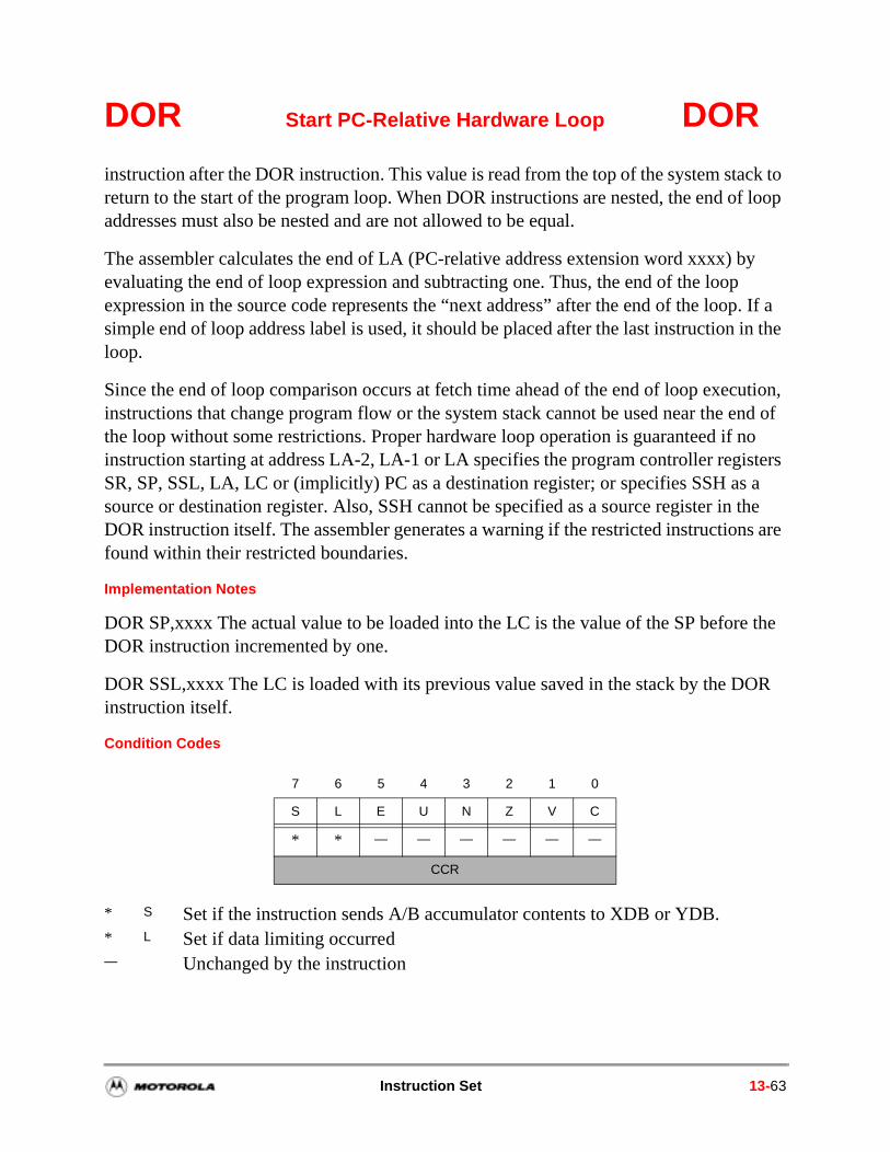
p. If a in the
ution, end of no ters a the s are
e the
OR
DOR Start PC-Relative Hardware Loop DOR
instruction after the DOR instruction. This value is read from the top of the system stack to return to the start of the program loop. When DOR instructions are nested, the end of loop addresses must also be nested and are not allowed to be equal.
The assembler calculates the end of LA (PC-relative address extension word xxxx) by evaluating the end of loop expression and subtracting one. Thus, the end of the loop expression in the source code represents the “next address” after the end of the loosimple end of loop address label is used, it should be placed after the last instructionloop.
Since the end of loop comparison occurs at fetch time ahead of the end of loop execinstructions that change program flow or the system stack cannot be used near the the loop without some restrictions. Proper hardware loop operation is guaranteed if instruction starting at address LA-2, LA-1 or LA specifies the program controller regisSR, SP, SSL, LA, LC or (implicitly) PC as a destination register; or specifies SSH assource or destination register. Also, SSH cannot be specified as a source register inDOR instruction itself. The assembler generates a warning if the restricted instructionfound within their restricted boundaries.
Implementation Notes
DOR SP,xxxx The actual value to be loaded into the LC is the value of the SP beforDOR instruction incremented by one.
DOR SSL,xxxx The LC is loaded with its previous value saved in the stack by the Dinstruction itself.
Condition Codes
7 6 5 4 3 2 1 0
S L E U N Z V C
* * — — — — — —
CCR
* S Set if the instruction sends A/B accumulator contents to XDB or YDB.* L Set if data limiting occurred — Unchanged by the instruction
Instruction Set 13-63
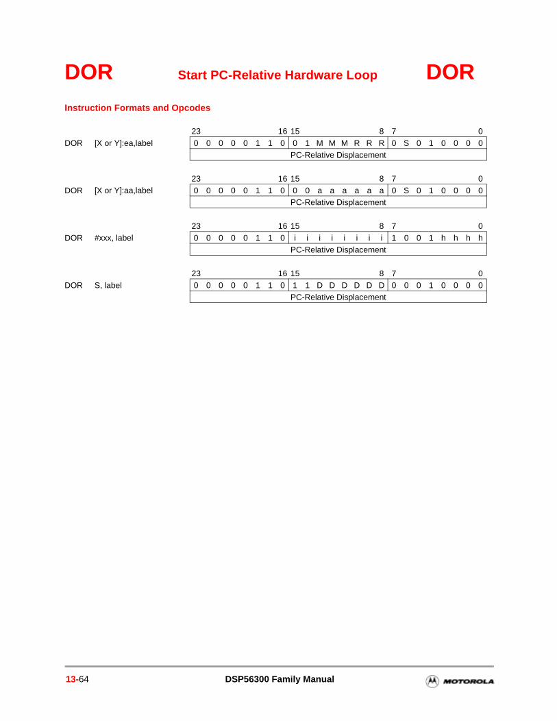
DOR Start PC-Relative Hardware Loop DORInstruction Formats and Opcodes
23 16 15 8 7 0
DOR [X or Y]:ea,label 0 0 0 0 0 1 1 0 0 1 M M M R R R 0 S 0 1 0 0 0 0PC-Relative Displacement
23 16 15 8 7 0DOR [X or Y]:aa,label 0 0 0 0 0 1 1 0 0 0 a a a a a a 0 S 0 1 0 0 0 0
PC-Relative Displacement
23 16 15 8 7 0DOR #xxx, label 0 0 0 0 0 1 1 0 i i i i i i i i 1 0 0 1 h h h h
PC-Relative Displacement
23 16 15 8 7 0
DOR S, label 0 0 0 0 0 1 1 0 1 1 D D D D D D 0 0 0 1 0 0 0 0PC-Relative Displacement
13-64 DSP56300 Family Manual
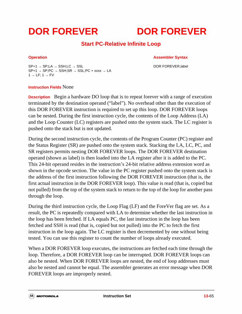
n of s A)
ister is
er and , and n C.
d as tack is
the but
r pass
s a ion in
ing
gh the can must en DOR
DOR FOREVER DOR FOREVERStart PC-Relative Infinite Loop
Instruction Fields None
Description Begin a hardware DO loop that is to repeat forever with a range of execution terminated by the destination operand (“label”). No overhead other than the executiothis DOR FOREVER instruction is required to set up this loop. DOR FOREVER loopcan be nested. During the first instruction cycle, the contents of the Loop Address (Land the Loop Counter (LC) registers are pushed onto the system stack. The LC regpushed onto the stack but is not updated.
During the second instruction cycle, the contents of the Program Counter (PC) registthe Status Register (SR) are pushed onto the system stack. Stacking the LA, LC, PCSR registers permits nesting DOR FOREVER loops. The DOR FOREVER destinatiooperand (shown as label) is then loaded into the LA register after it is added to the PThis 24-bit operand resides in the instruction’s 24-bit relative address extension worshown in the opcode section. The value in the PC register pushed onto the system sthe address of the first instruction following the DOR FOREVER instruction (that is, first actual instruction in the DOR FOREVER loop). This value is read (that is, copiednot pulled) from the top of the system stack to return to the top of the loop for anothethrough the loop.
During the third instruction cycle, the Loop Flag (LF) and the ForeVer flag are set. Aresult, the PC is repeatedly compared with LA to determine whether the last instructthe loop has been fetched. If LA equals PC, the last instruction in the loop has beenfetched and SSH is read (that is, copied but not pulled) into the PC to fetch the first instruction in the loop again. The LC register is then decremented by one without betested. You can use this register to count the number of loops already executed.
When a DOR FOREVER loop executes, the instructions are fetched each time throuloop. Therefore, a DOR FOREVER loop can be interrupted. DOR FOREVER loops also be nested. When DOR FOREVER loops are nested, the end of loop addressesalso be nested and cannot be equal. The assembler generates an error message whFOREVER loops are improperly nested.
Operation Assembler Syntax
SP+1 → SP;LA → SSH;LC → SSL DOR FOREVER,labelSP+1 → SP;PC → SSH;SR → SSL;PC + xxxx → LA1 → LF; 1 → FV
Instruction Set 13-65
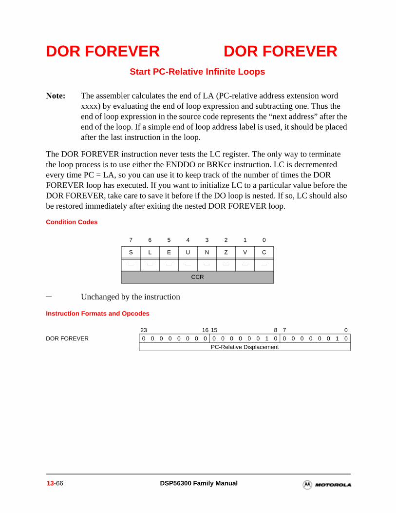
ter the laced
ate ed the also
DOR FOREVER DOR FOREVERStart PC-Relative Infinite Loops
Note: The assembler calculates the end of LA (PC-relative address extension word xxxx) by evaluating the end of loop expression and subtracting one. Thus the end of loop expression in the source code represents the “next address” afend of the loop. If a simple end of loop address label is used, it should be pafter the last instruction in the loop.
The DOR FOREVER instruction never tests the LC register. The only way to terminthe loop process is to use either the ENDDO or BRKcc instruction. LC is decrementevery time PC = LA, so you can use it to keep track of the number of times the DORFOREVER loop has executed. If you want to initialize LC to a particular value beforeDOR FOREVER, take care to save it before if the DO loop is nested. If so, LC shouldbe restored immediately after exiting the nested DOR FOREVER loop.
Condition Codes
Instruction Formats and Opcodes
7 6 5 4 3 2 1 0
S L E U N Z V C
— — — — — — — —
CCR
— Unchanged by the instruction
23 16 15 8 7 0DOR FOREVER 0 0 0 0 0 0 0 0 0 0 0 0 0 0 1 0 0 0 0 0 0 0 1 0
PC-Relative Displacement
13-66 DSP56300 Family Manual
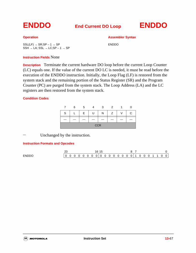
ENDDO End Current DO Loop ENDDO
Instruction Fields None
Description Terminate the current hardware DO loop before the current Loop Counter (LC) equals one. If the value of the current DO LC is needed, it must be read before the execution of the ENDDO instruction. Initially, the Loop Flag (LF) is restored from the system stack and the remaining portion of the Status Register (SR) and the Program Counter (PC) are purged from the system stack. The Loop Address (LA) and the LC registers are then restored from the system stack.
Condition Codes
Instruction Formats and Opcodes
Operation Assembler Syntax
SSL(LF) → SR;SP – 1 → SP ENDDOSSH → LA; SSL → LC;SP – 1 → SP
7 6 5 4 3 2 1 0
S L E U N Z V C
— — — — — — — —
CCR
— Unchanged by the instruction.
23 16 15 8 7 0
ENDDO 0 0 0 0 0 0 0 0 0 0 0 0 0 0 0 0 1 0 0 0 1 1 0 0
Instruction Set 13-67
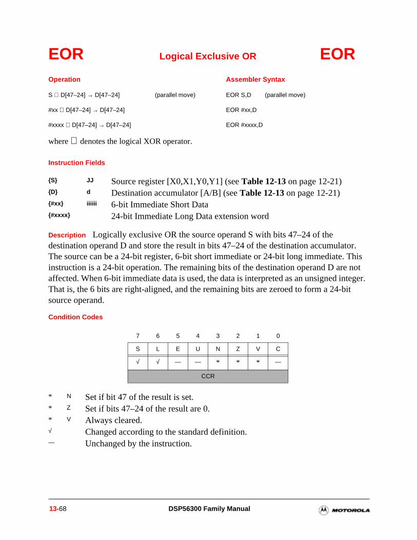
tor. This not nteger. it
EOR Logical Exclusive OR EOR
Instruction Fields
Description Logically exclusive OR the source operand S with bits 47–24 of the destination operand D and store the result in bits 47–24 of the destination accumulaThe source can be a 24-bit register, 6-bit short immediate or 24-bit long immediate. instruction is a 24-bit operation. The remaining bits of the destination operand D areaffected. When 6-bit immediate data is used, the data is interpreted as an unsigned iThat is, the 6 bits are right-aligned, and the remaining bits are zeroed to form a 24-bsource operand.
Condition Codes
Operation Assembler Syntax
S ⊕ D[47–24] → D[47–24] (parallel move) EOR S,D (parallel move)
#xx ⊕ D[47–24] → D[47–24] EOR #xx,D
#xxxx ⊕ D[47–24] → D[47–24] EOR #xxxx,D
where ⊕ denotes the logical XOR operator.
S JJ Source register [X0,X1,Y0,Y1] (see Table 12-13 on page 12-21)D d Destination accumulator [A/B] (see Table 12-13 on page 12-21)#xx iiiiii 6-bit Immediate Short Data #xxxx 24-bit Immediate Long Data extension word
7 6 5 4 3 2 1 0
S L E U N Z V C
√ √ — — * * * —
CCR
* N Set if bit 47 of the result is set.* Z Set if bits 47–24 of the result are 0.* V Always cleared.√ Changed according to the standard definition.— Unchanged by the instruction.
13-68 DSP56300 Family Manual
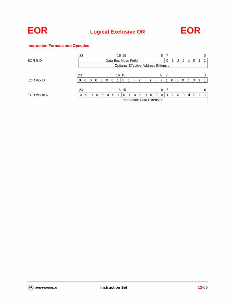
EOR Logical Exclusive OR EORInstruction Formats and Opcodes
23 16 15 8 7 0
EOR S,D Data Bus Move Field 0 1 J J d 0 1 1Optional Effective Address Extension
23 16 15 8 7 0
EOR #xx,D 0 0 0 0 0 0 0 1 0 1 i i i i i i 1 0 0 0 d 0 1 1
23 16 15 8 7 0EOR #xxxx,D 0 0 0 0 0 0 0 1 0 1 0 0 0 0 0 0 1 1 0 0 d 0 1 1
Immediate Data Extension
Instruction Set 13-69
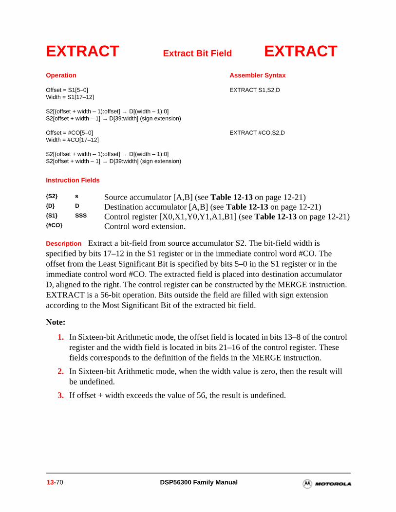
e tor tion.
trol se
ill
EXTRACT Extract Bit Field EXTRACT
Instruction Fields
Description Extract a bit-field from source accumulator S2. The bit-field width is specified by bits 17–12 in the S1 register or in the immediate control word #CO. The offset from the Least Significant Bit is specified by bits 5–0 in the S1 register or in thimmediate control word #CO. The extracted field is placed into destination accumulaD, aligned to the right. The control register can be constructed by the MERGE instrucEXTRACT is a 56-bit operation. Bits outside the field are filled with sign extension according to the Most Significant Bit of the extracted bit field.
Note:
1. In Sixteen-bit Arithmetic mode, the offset field is located in bits 13–8 of the conregister and the width field is located in bits 21–16 of the control register. Thefields corresponds to the definition of the fields in the MERGE instruction.
2. In Sixteen-bit Arithmetic mode, when the width value is zero, then the result wbe undefined.
3. If offset + width exceeds the value of 56, the result is undefined.
Operation Assembler Syntax
Offset = S1[5–0] EXTRACT S1,S2,DWidth = S1[17–12]
S2[(offset + width – 1):offset] → D[(width – 1):0]S2[offset + width – 1] → D[39:width] (sign extension)
Offset = #CO[5–0] Width = #CO[17–12]
EXTRACT #CO,S2,D
S2[(offset + width – 1):offset] → D[(width – 1):0]S2[offset + width – 1] → D[39:width] (sign extension)
S2 s Source accumulator [A,B] (see Table 12-13 on page 12-21)D D Destination accumulator [A,B] (see Table 12-13 on page 12-21)S1 SSS Control register [X0,X1,Y0,Y1,A1,B1] (see Table 12-13 on page 12-21)#CO Control word extension.
13-70 DSP56300 Family Manual
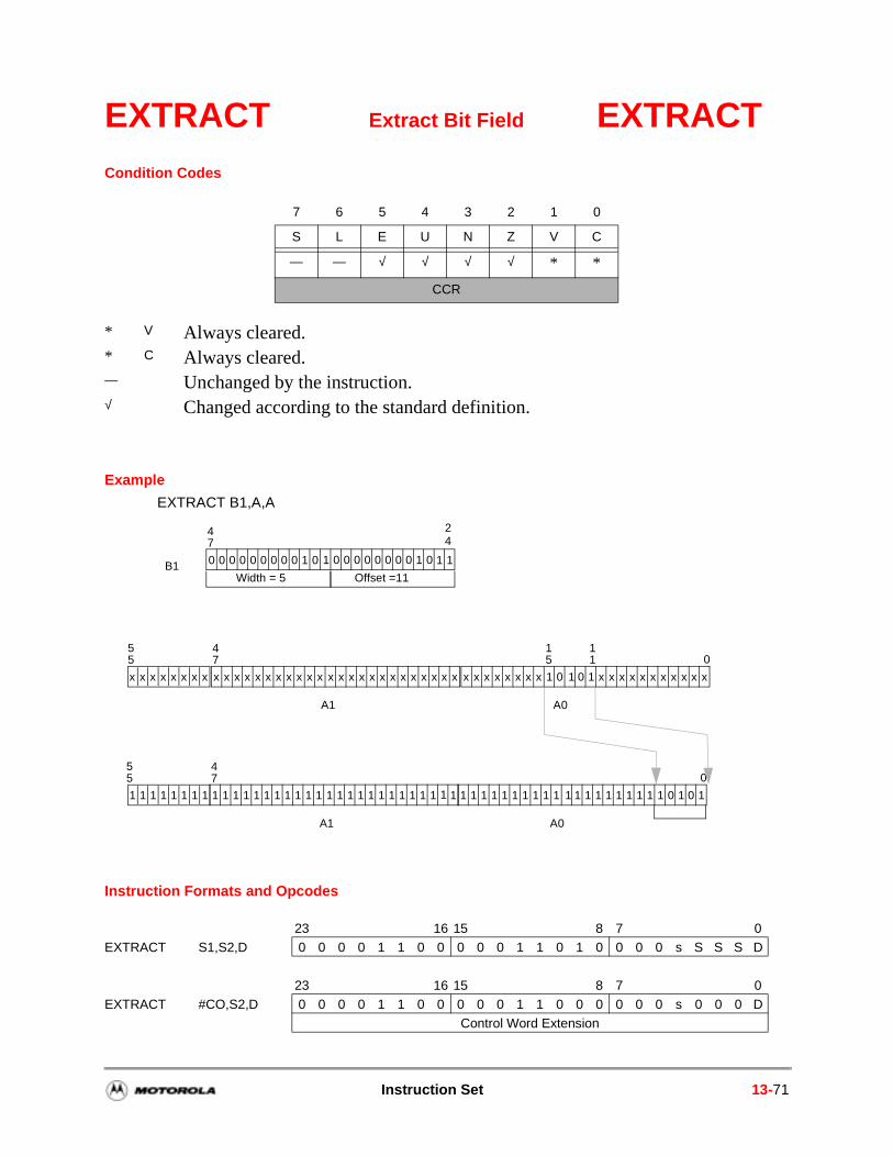
EXTRACT Extract Bit Field EXTRACTCondition Codes
Example
Instruction Formats and Opcodes
7 6 5 4 3 2 1 0
S L E U N Z V C
— — √ √ √ √ * *
CCR
* V Always cleared.* C Always cleared.— Unchanged by the instruction.√ Changed according to the standard definition.
23 16 15 8 7 0EXTRACT S1,S2,D 0 0 0 0 1 1 0 0 0 0 0 1 1 0 1 0 0 0 0 s S S S D
23 16 15 8 7 0EXTRACT #CO,S2,D 0 0 0 0 1 1 0 0 0 0 0 1 1 0 0 0 0 0 0 s 0 0 0 D
Control Word Extension
EXTRACT B1,A,A
B1 0 0 0 0 0 0 0 0 0 1 0 1 0 0 0 0 0 0 0 0 1 0 1 1
47
24
Offset =11Width = 5
x x x x x x x x 1 0 1 0 1 x x x x x x x x x x xx x x x x x x x x x x x x x x x x x x x x x x x
47 0
A1 A0
1 1 1 1 1 1 1 1 1 1 1 1 1 1 1 1 1 1 1 1 0 1 0 11 1 1 1 1 1 1 1 1 1 1 1 1 1 1 1 1 1 1 1 1 1 1
47 0
A1 A0
11 1 1 1 1 1 1 1
x x x x x x x x
55
55
51
11
Instruction Set 13-71
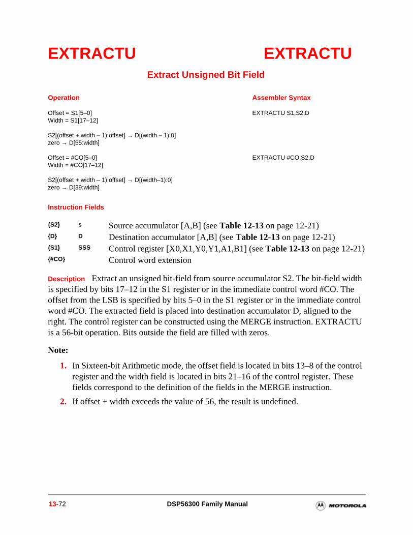
e ntrol e TU
trol se
EXTRACTU EXTRACTUExtract Unsigned Bit Field
Instruction Fields
Description Extract an unsigned bit-field from source accumulator S2. The bit-field width is specified by bits 17–12 in the S1 register or in the immediate control word #CO. Thoffset from the LSB is specified by bits 5–0 in the S1 register or in the immediate coword #CO. The extracted field is placed into destination accumulator D, aligned to thright. The control register can be constructed using the MERGE instruction. EXTRACis a 56-bit operation. Bits outside the field are filled with zeros.
Note:
1. In Sixteen-bit Arithmetic mode, the offset field is located in bits 13–8 of the conregister and the width field is located in bits 21–16 of the control register. Thefields correspond to the definition of the fields in the MERGE instruction.
2. If offset + width exceeds the value of 56, the result is undefined.
Operation Assembler Syntax
Offset = S1[5–0] EXTRACTU S1,S2,DWidth = S1[17–12]
S2[(offset + width – 1):offset] → D[(width – 1):0]zero → D[55:width]
Offset = #CO[5–0] EXTRACTU #CO,S2,DWidth = #CO[17–12]
S2[(offset + width – 1):offset] → D[(width–1):0]zero → D[39:width]
S2 s Source accumulator [A,B] (see Table 12-13 on page 12-21)D D Destination accumulator [A,B] (see Table 12-13 on page 12-21)S1 SSS Control register [X0,X1,Y0,Y1,A1,B1] (see Table 12-13 on page 12-21)#CO Control word extension
13-72 DSP56300 Family Manual
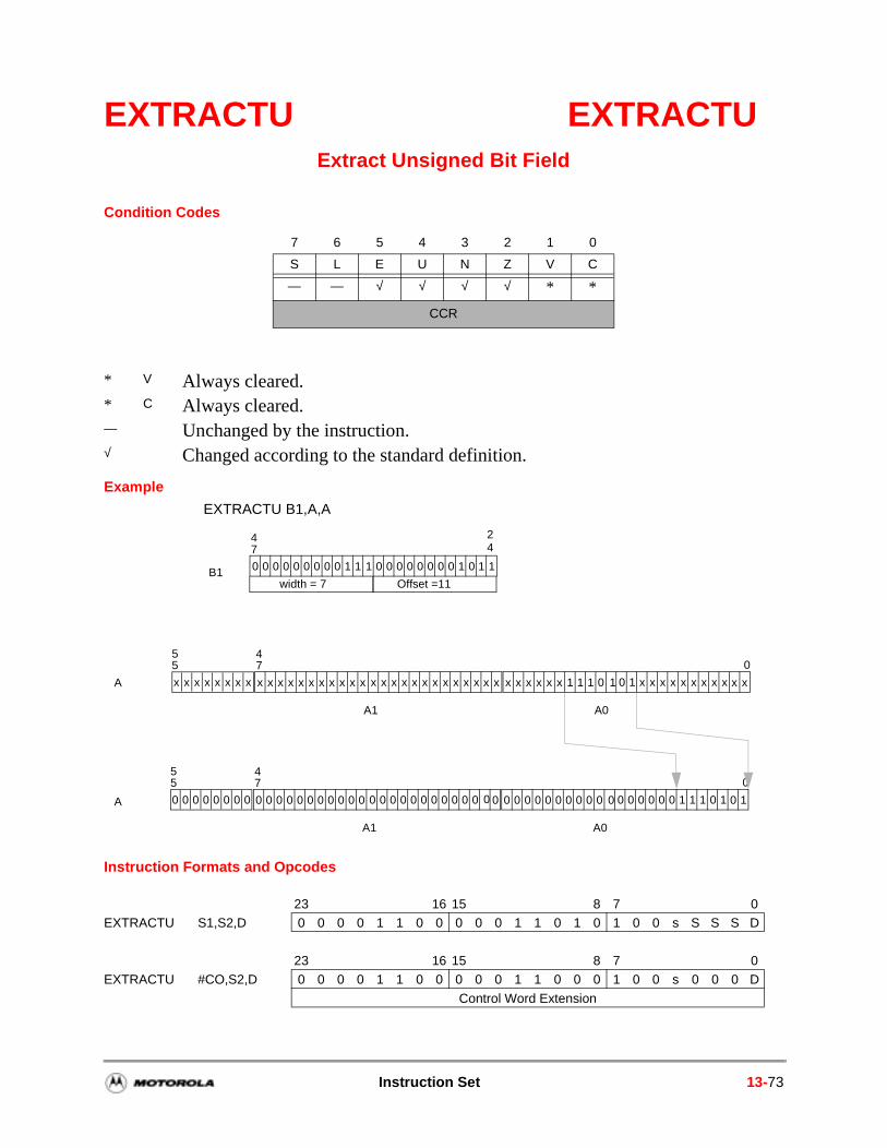
EXTRACTU EXTRACTUExtract Unsigned Bit Field
Condition Codes
Example
Instruction Formats and Opcodes
7 6 5 4 3 2 1 0
S L E U N Z V C
— — √ √ √ √ * *
CCR
* V Always cleared.* C Always cleared.— Unchanged by the instruction.√ Changed according to the standard definition.
23 16 15 8 7 0EXTRACTU S1,S2,D 0 0 0 0 1 1 0 0 0 0 0 1 1 0 1 0 1 0 0 s S S S D
23 16 15 8 7 0EXTRACTU #CO,S2,D 0 0 0 0 1 1 0 0 0 0 0 1 1 0 0 0 1 0 0 s 0 0 0 D
Control Word Extension
EXTRACTU B1,A,A
B1 0 0 0 0 0 0 0 0 0 1 1 1 0 0 0 0 0 0 0 0 1 0 1 1
47
24
Offset =11width = 7
x x x x x x 1 1 1 0 1 0 1 x x x x x x x x x x xx x x x x x x x x x x x x x x x x x x x x x x x
47 0
A
A1 A0
0 0 0 0 0 0 0 0 0 0 0 0 0 0 0 0 0 1 1 1 0 1 0 10 0 0 0 0 0 0 0 0 0 0 0 0 0 0 0 0 0 0 0 0 0 0
47 0
A
A1 A0
00 0 0 0 0 0 0 0
x x x x x x x x
55
55
Instruction Set 13-73
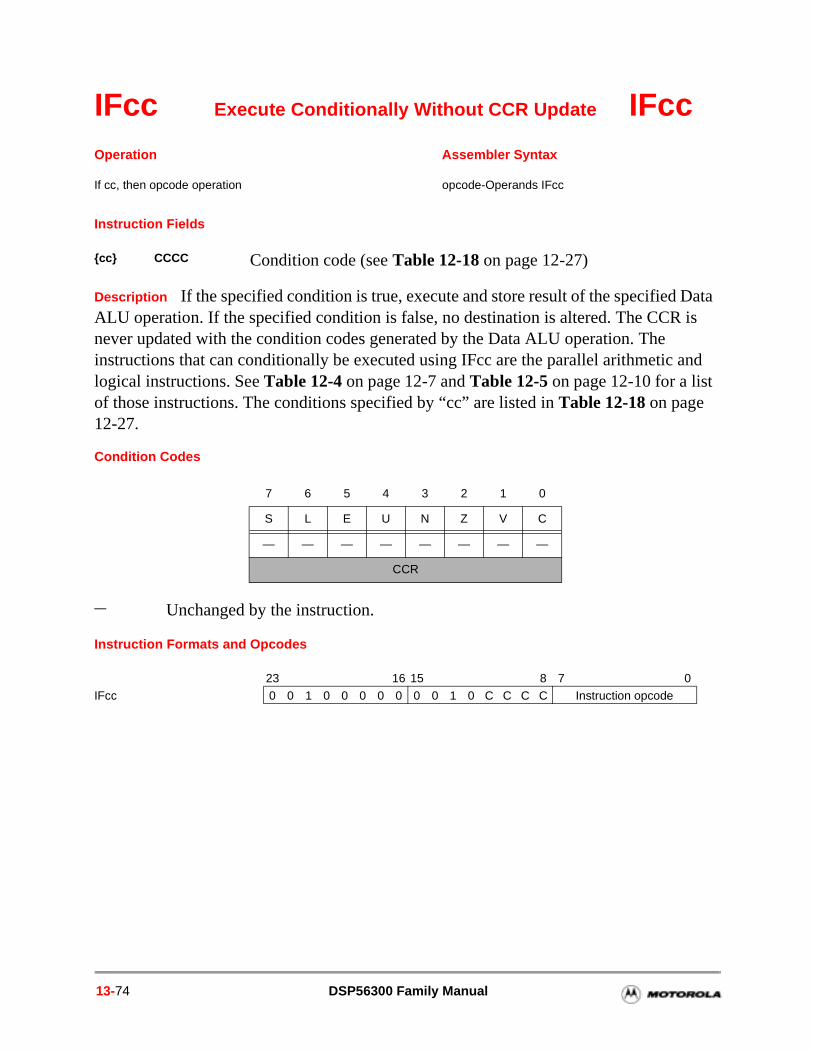
IFcc Execute Conditionally Without CCR Update IFcc
Instruction Fields
Description If the specified condition is true, execute and store result of the specified Data ALU operation. If the specified condition is false, no destination is altered. The CCR is never updated with the condition codes generated by the Data ALU operation. The instructions that can conditionally be executed using IFcc are the parallel arithmetic and logical instructions. See Table 12-4 on page 12-7 and Table 12-5 on page 12-10 for a list of those instructions. The conditions specified by “cc” are listed in Table 12-18 on page 12-27.
Condition Codes
Instruction Formats and Opcodes
Operation Assembler Syntax
If cc, then opcode operation opcode-Operands IFcc
cc CCCC Condition code (see Table 12-18 on page 12-27)
7 6 5 4 3 2 1 0
S L E U N Z V C
— — — — — — — —
CCR
— Unchanged by the instruction.
23 16 15 8 7 0
IFcc 0 0 1 0 0 0 0 0 0 0 1 0 C C C C Instruction opcode
13-74 DSP56300 Family Manual
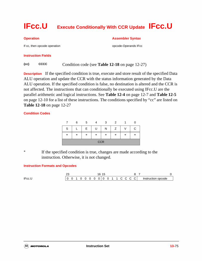
d on
IFcc.U Execute Conditionally With CCR Update IFcc.U
Instruction Fields
Description If the specified condition is true, execute and store result of the specified Data ALU operation and update the CCR with the status information generated by the Data ALU operation. If the specified condition is false, no destination is altered and the CCR is not affected. The instructions that can conditionally be executed using IFcc.U are the parallel arithmetic and logical instructions. See Table 12-4 on page 12-7 and Table 12-5 on page 12-10 for a list of these instructions. The conditions specified by “cc” are listeTable 12-18 on page 12-27
Condition Codes
Instruction Formats and Opcodes
Operation Assembler Syntax
If cc, then opcode operation opcode-Operands IFcc
cc CCCC Condition code (see Table 12-18 on page 12-27)
7 6 5 4 3 2 1 0
S L E U N Z V C
* * * * * * * *
CCR
* If the specified condition is true, changes are made according to the instruction. Otherwise, it is not changed.
23 16 15 8 7 0
IFcc.U 0 0 1 0 0 0 0 0 0 0 1 1 C C C C Instruction opcode
Instruction Set 13-75
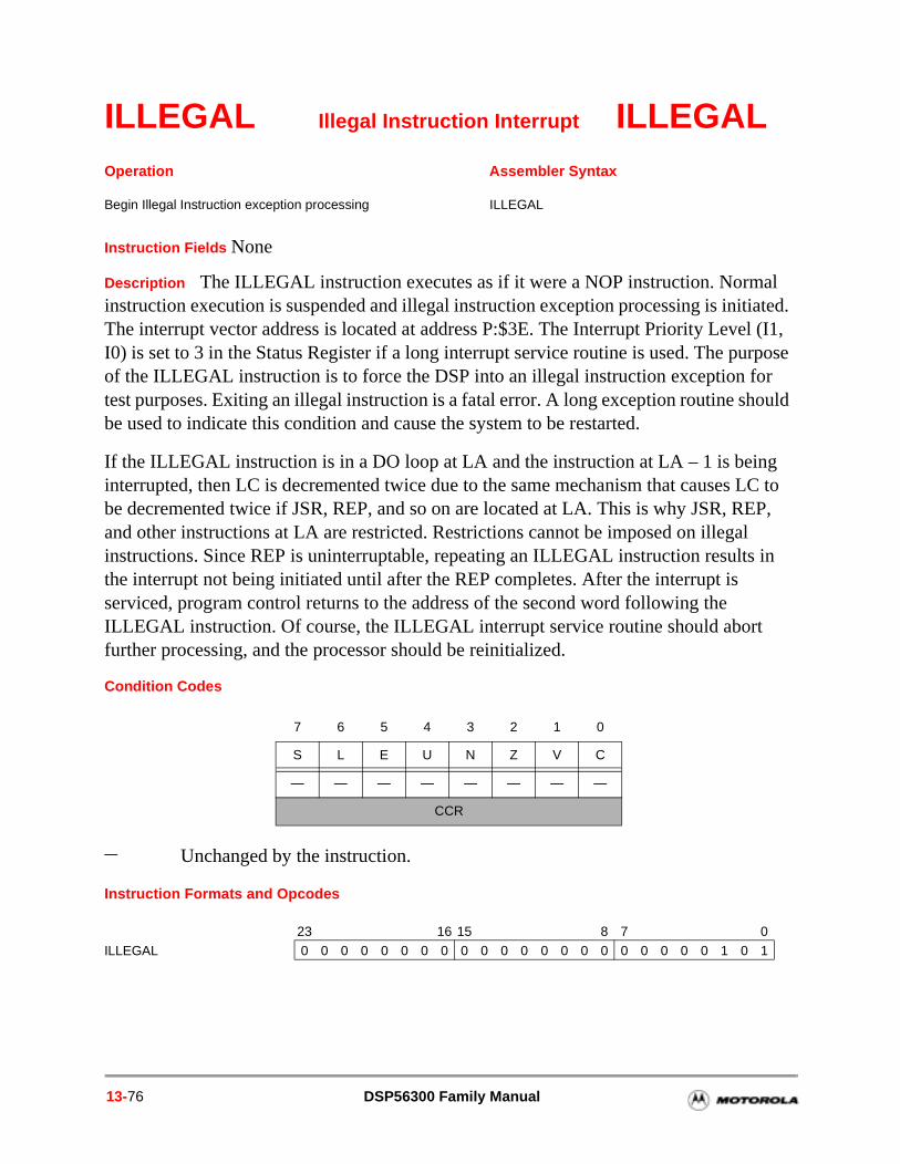
LC to EP, l in
ILLEGAL Illegal Instruction Interrupt ILLEGAL
Instruction Fields None
Description The ILLEGAL instruction executes as if it were a NOP instruction. Normal instruction execution is suspended and illegal instruction exception processing is initiated. The interrupt vector address is located at address P:$3E. The Interrupt Priority Level (I1, I0) is set to 3 in the Status Register if a long interrupt service routine is used. The purpose of the ILLEGAL instruction is to force the DSP into an illegal instruction exception for test purposes. Exiting an illegal instruction is a fatal error. A long exception routine should be used to indicate this condition and cause the system to be restarted.
If the ILLEGAL instruction is in a DO loop at LA and the instruction at LA – 1 is beinginterrupted, then LC is decremented twice due to the same mechanism that causes be decremented twice if JSR, REP, and so on are located at LA. This is why JSR, Rand other instructions at LA are restricted. Restrictions cannot be imposed on illegainstructions. Since REP is uninterruptable, repeating an ILLEGAL instruction resultsthe interrupt not being initiated until after the REP completes. After the interrupt is serviced, program control returns to the address of the second word following the ILLEGAL instruction. Of course, the ILLEGAL interrupt service routine should abort further processing, and the processor should be reinitialized.
Condition Codes
Instruction Formats and Opcodes
Operation Assembler Syntax
Begin Illegal Instruction exception processing ILLEGAL
7 6 5 4 3 2 1 0
S L E U N Z V C
— — — — — — — —
CCR
— Unchanged by the instruction.
23 16 15 8 7 0
ILLEGAL 0 0 0 0 0 0 0 0 0 0 0 0 0 0 0 0 0 0 0 0 0 1 0 1
13-76 DSP56300 Family Manual
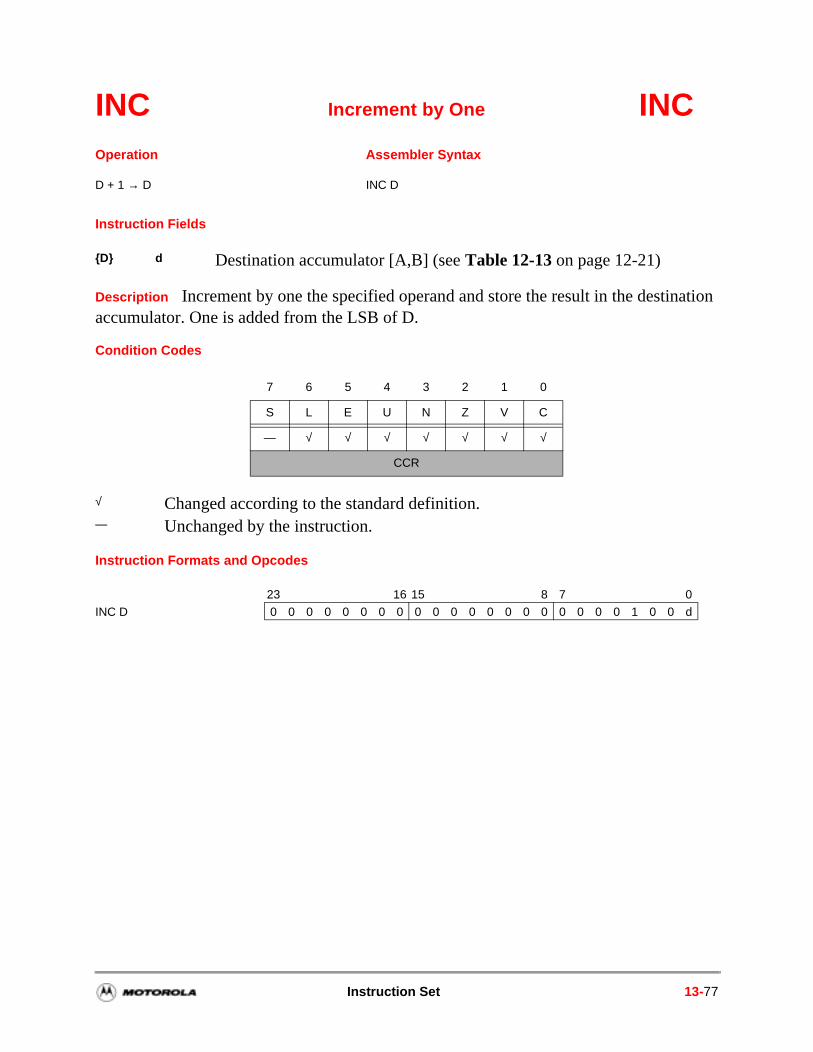
INC Increment by One INC
Instruction Fields
Description Increment by one the specified operand and store the result in the destination accumulator. One is added from the LSB of D.
Condition Codes
Instruction Formats and Opcodes
Operation Assembler Syntax
D + 1 → D INC D
D d Destination accumulator [A,B] (see Table 12-13 on page 12-21)
7 6 5 4 3 2 1 0
S L E U N Z V C
— √ √ √ √ √ √ √
CCR
√ Changed according to the standard definition.— Unchanged by the instruction.
23 16 15 8 7 0
INC D 0 0 0 0 0 0 0 0 0 0 0 0 0 0 0 0 0 0 0 0 1 0 0 d
Instruction Set 13-77
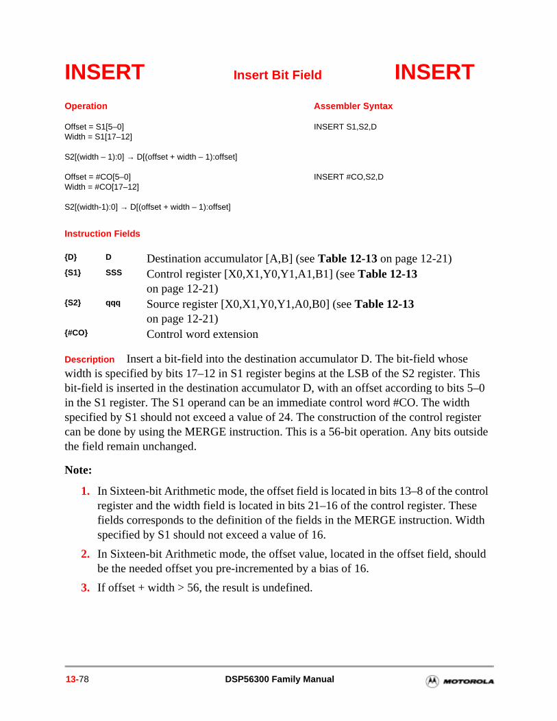
is 5–0 th ister tside
trol se th
uld
INSERT Insert Bit Field INSERT
Instruction Fields
Description Insert a bit-field into the destination accumulator D. The bit-field whose width is specified by bits 17–12 in S1 register begins at the LSB of the S2 register. Thbit-field is inserted in the destination accumulator D, with an offset according to bits in the S1 register. The S1 operand can be an immediate control word #CO. The widspecified by S1 should not exceed a value of 24. The construction of the control regcan be done by using the MERGE instruction. This is a 56-bit operation. Any bits outhe field remain unchanged.
Note:
1. In Sixteen-bit Arithmetic mode, the offset field is located in bits 13–8 of the conregister and the width field is located in bits 21–16 of the control register. Thefields corresponds to the definition of the fields in the MERGE instruction. Widspecified by S1 should not exceed a value of 16.
2. In Sixteen-bit Arithmetic mode, the offset value, located in the offset field, shobe the needed offset you pre-incremented by a bias of 16.
3. If offset + width > 56, the result is undefined.
Operation Assembler Syntax
Offset = S1[5–0] Width = S1[17–12]
INSERT S1,S2,D
S2[(width – 1):0] → D[(offset + width – 1):offset]
Offset = #CO[5–0] Width = #CO[17–12]
INSERT #CO,S2,D
S2[(width-1):0] → D[(offset + width – 1):offset]
D D Destination accumulator [A,B] (see Table 12-13 on page 12-21)S1 SSS Control register [X0,X1,Y0,Y1,A1,B1] (see Table 12-13
on page 12-21)S2 qqq Source register [X0,X1,Y0,Y1,A0,B0] (see Table 12-13
on page 12-21)#CO Control word extension
13-78 DSP56300 Family Manual
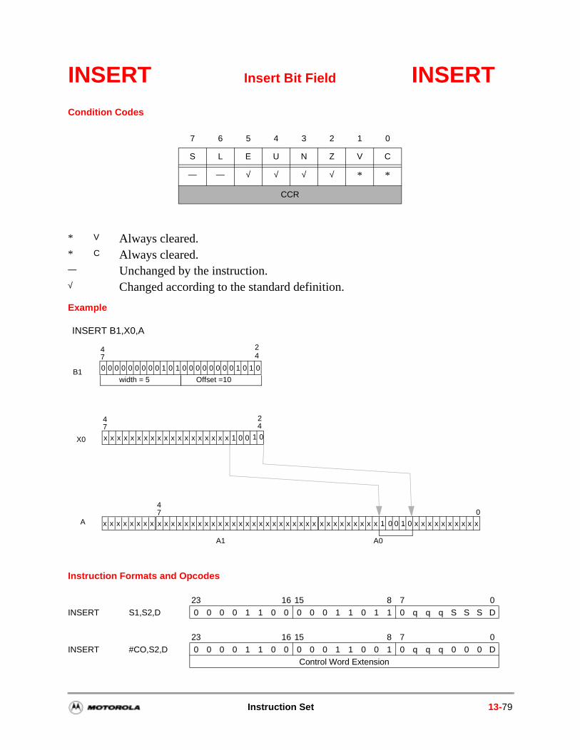
INSERT Insert Bit Field INSERTCondition Codes
Example
Instruction Formats and Opcodes
7 6 5 4 3 2 1 0
S L E U N Z V C
— — √ √ √ √ * *
CCR
* V Always cleared.* C Always cleared.— Unchanged by the instruction.√ Changed according to the standard definition.
23 16 15 8 7 0
INSERT S1,S2,D 0 0 0 0 1 1 0 0 0 0 0 1 1 0 1 1 0 q q q S S S D
23 16 15 8 7 0
INSERT #CO,S2,D 0 0 0 0 1 1 0 0 0 0 0 1 1 0 0 1 0 q q q 0 0 0 DControl Word Extension
INSERT B1,X0,A
B1 0 0 0 0 0 0 0 0 0 1 0 1 0 0 0 0 0 0 0 0 1 0 1 0
47
24
Offset =10width = 5
x x x x x x x x x x x x x x x x x x x 1 0 0 1 0
447
X0
2
x x x x x x x x x 1 0 0 1 0 x x x x x x x x x xx x x x x x x x x x x x x x x x x x x x x x x x
47 0
A
A1 A0
x x x x x x x x
Instruction Set 13-79
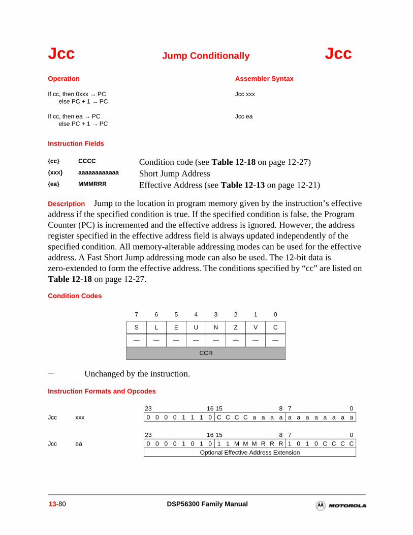
tive am ress e ctive
ed on
Jcc Jump Conditionally Jcc
Instruction Fields
Description Jump to the location in program memory given by the instruction’s effecaddress if the specified condition is true. If the specified condition is false, the ProgrCounter (PC) is incremented and the effective address is ignored. However, the addregister specified in the effective address field is always updated independently of thspecified condition. All memory-alterable addressing modes can be used for the effeaddress. A Fast Short Jump addressing mode can also be used. The 12-bit data is zero-extended to form the effective address. The conditions specified by “cc” are listTable 12-18 on page 12-27.
Condition Codes
Instruction Formats and Opcodes
Operation Assembler Syntax
If cc, then 0xxx → PC Jcc xxxelse PC + 1 → PC
If cc, then ea → PC Jcc eaelse PC + 1 → PC
cc CCCC Condition code (see Table 12-18 on page 12-27)xxx aaaaaaaaaaaa Short Jump Addressea MMMRRR Effective Address (see Table 12-13 on page 12-21)
7 6 5 4 3 2 1 0
S L E U N Z V C
— — — — — — — —
CCR
— Unchanged by the instruction.
23 16 15 8 7 0Jcc xxx 0 0 0 0 1 1 1 0 C C C C a a a a a a a a a a a a
23 16 15 8 7 0Jcc ea 0 0 0 0 1 0 1 0 1 1 M M M R R R 1 0 1 0 C C C C
Optional Effective Address Extension
13-80 DSP56300 Family Manual
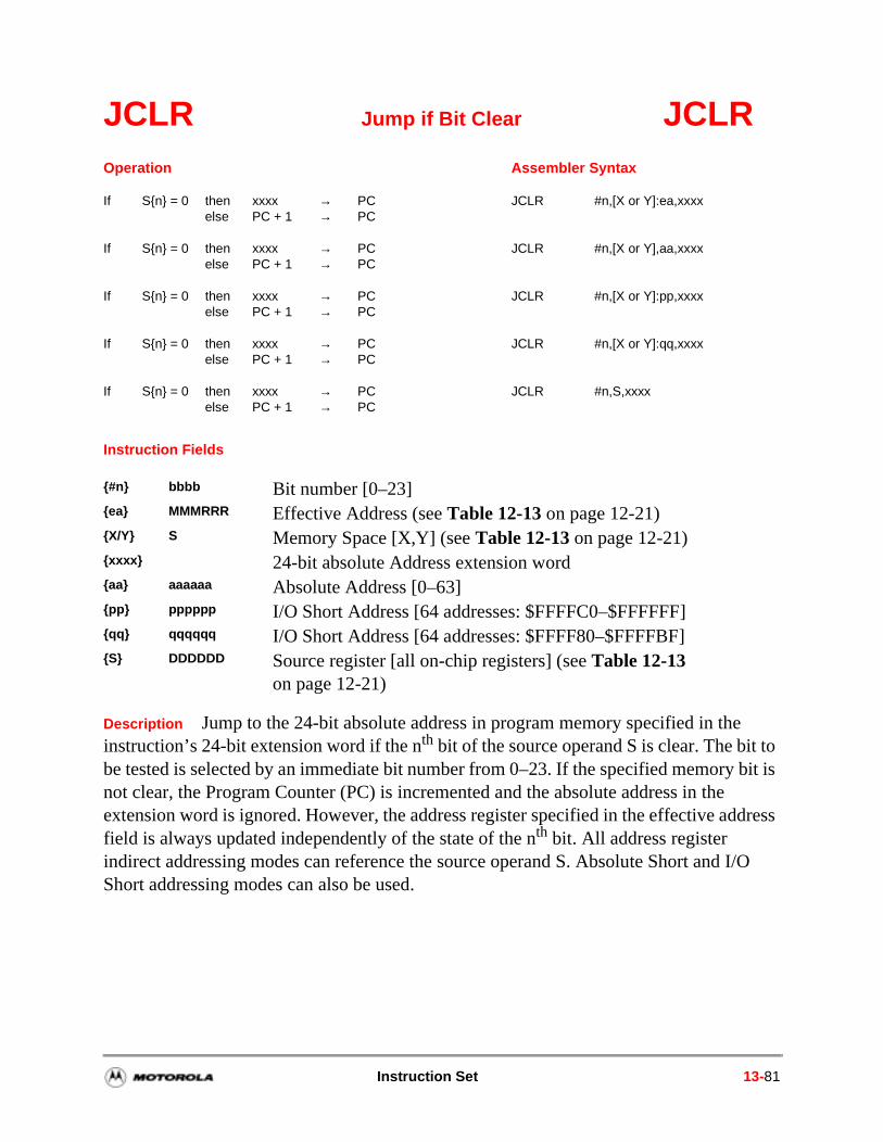
to bit is dress
I/O
JCLR Jump if Bit Clear JCLR
Instruction Fields
Description Jump to the 24-bit absolute address in program memory specified in the instruction’s 24-bit extension word if the nth bit of the source operand S is clear. The bit be tested is selected by an immediate bit number from 0–23. If the specified memorynot clear, the Program Counter (PC) is incremented and the absolute address in theextension word is ignored. However, the address register specified in the effective adfield is always updated independently of the state of the nth bit. All address register indirect addressing modes can reference the source operand S. Absolute Short andShort addressing modes can also be used.
Operation Assembler Syntax
If Sn = 0 then xxxx → PC JCLR #n,[X or Y]:ea,xxxxelse PC + 1 → PC
If Sn = 0 then xxxx → PC JCLR #n,[X or Y],aa,xxxxelse PC + 1 → PC
If Sn = 0 then xxxx → PC JCLR #n,[X or Y]:pp,xxxxelse PC + 1 → PC
If Sn = 0 then xxxx → PC JCLR #n,[X or Y]:qq,xxxxelse PC + 1 → PC
If Sn = 0 then xxxx → PC JCLR #n,S,xxxxelse PC + 1 → PC
#n bbbb Bit number [0–23]ea MMMRRR Effective Address (see Table 12-13 on page 12-21)X/Y S Memory Space [X,Y] (see Table 12-13 on page 12-21)xxxx 24-bit absolute Address extension wordaa aaaaaa Absolute Address [0–63]pp pppppp I/O Short Address [64 addresses: $FFFFC0–$FFFFFF]qq qqqqqq I/O Short Address [64 addresses: $FFFF80–$FFFFBF]S DDDDDD Source register [all on-chip registers] (see Table 12-13
on page 12-21)
Instruction Set 13-81
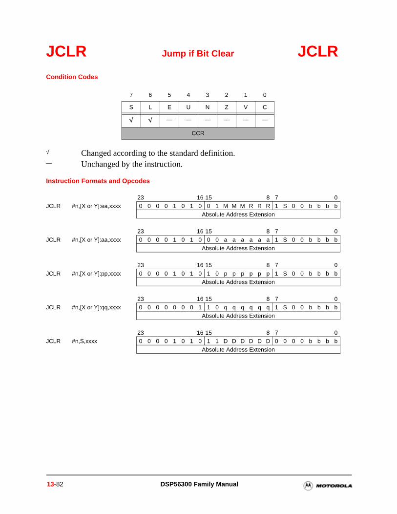
JCLR Jump if Bit Clear JCLRCondition Codes
Instruction Formats and Opcodes
7 6 5 4 3 2 1 0
S L E U N Z V C
√ √ — — — — — —
CCR
√ Changed according to the standard definition. — Unchanged by the instruction.
23 16 15 8 7 0JCLR #n,[X or Y]:ea,xxxx 0 0 0 0 1 0 1 0 0 1 M M M R R R 1 S 0 0 b b b b
Absolute Address Extension
23 16 15 8 7 0JCLR #n,[X or Y]:aa,xxxx 0 0 0 0 1 0 1 0 0 0 a a a a a a 1 S 0 0 b b b b
Absolute Address Extension
23 16 15 8 7 0
JCLR #n,[X or Y]:pp,xxxx 0 0 0 0 1 0 1 0 1 0 p p p p p p 1 S 0 0 b b b bAbsolute Address Extension
23 16 15 8 7 0JCLR #n,[X or Y]:qq,xxxx 0 0 0 0 0 0 0 1 1 0 q q q q q q 1 S 0 0 b b b b
Absolute Address Extension
23 16 15 8 7 0JCLR #n,S,xxxx 0 0 0 0 1 0 1 0 1 1 D D D D D D 0 0 0 0 b b b b
Absolute Address Extension
13-82 DSP56300 Family Manual
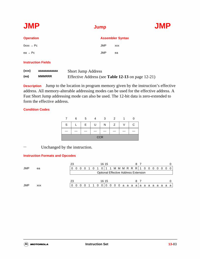
tive ess. A ed to
JMP Jump JMP
Instruction Fields
Description Jump to the location in program memory given by the instruction’s effecaddress. All memory-alterable addressing modes can be used for the effective addrFast Short Jump addressing mode can also be used. The 12-bit data is zero-extendform the effective address.
Condition Codes
Instruction Formats and Opcodes
Operation Assembler Syntax
0xxx → Pc JMP xxx
ea → Pc JMP ea
xxx aaaaaaaaaaaa Short Jump Addressea MMMRRR Effective Address (see Table 12-13 on page 12-21)
7 6 5 4 3 2 1 0
S L E U N Z V C
— — — — — — — —
CCR
— Unchanged by the instruction.
23 16 15 8 7 0
JMP ea 0 0 0 0 1 0 1 0 1 1 M M M R R R 1 0 0 0 0 0 0 0Optional Effective Address Extension
23 16 15 8 7 0JMP xxx 0 0 0 0 1 1 0 0 0 0 0 0 a a a a a a a a a a a a
Instruction Set 13-83
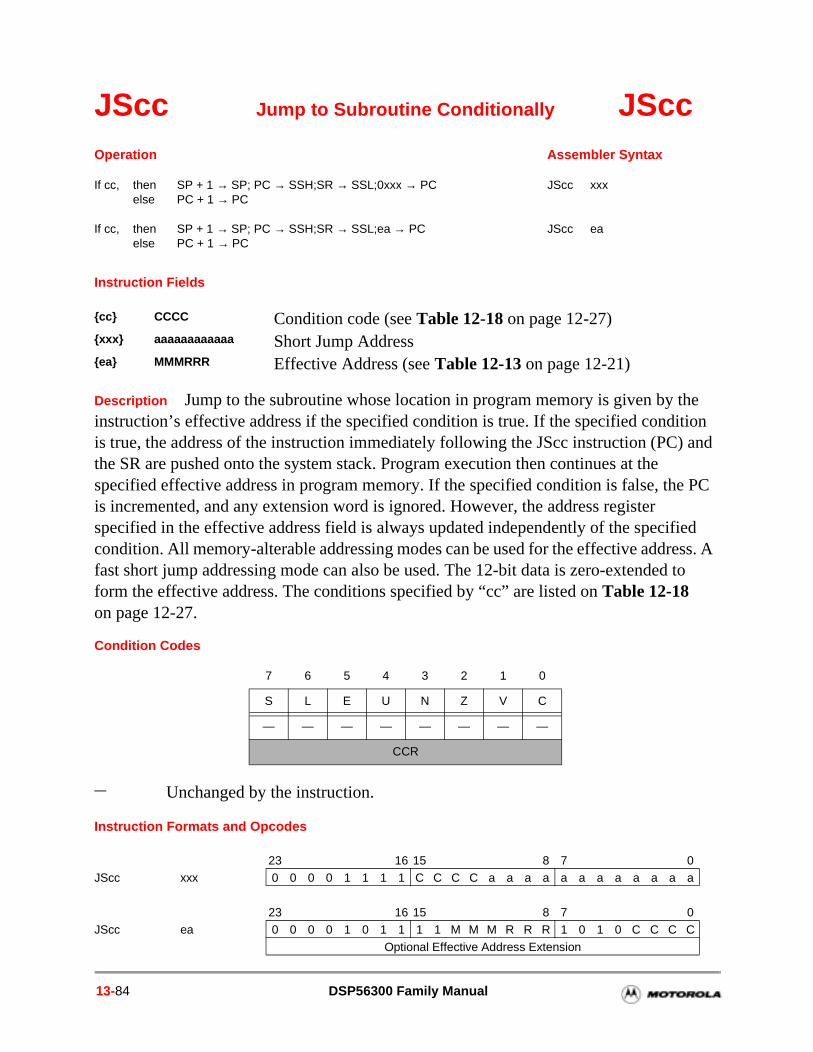
ion ) and e PC
ied ess. A to
JScc Jump to Subroutine Conditionally JScc
Instruction Fields
Description Jump to the subroutine whose location in program memory is given by the instruction’s effective address if the specified condition is true. If the specified conditis true, the address of the instruction immediately following the JScc instruction (PCthe SR are pushed onto the system stack. Program execution then continues at thespecified effective address in program memory. If the specified condition is false, this incremented, and any extension word is ignored. However, the address register specified in the effective address field is always updated independently of the specifcondition. All memory-alterable addressing modes can be used for the effective addrfast short jump addressing mode can also be used. The 12-bit data is zero-extendedform the effective address. The conditions specified by “cc” are listed on Table 12-18 on page 12-27.
Condition Codes
Instruction Formats and Opcodes
Operation Assembler Syntax
If cc, then SP + 1 → SP; PC → SSH;SR → SSL;0xxx → PC JScc xxxelse PC + 1 → PC
If cc, then SP + 1 → SP; PC → SSH;SR → SSL;ea → PC JScc eaelse PC + 1 → PC
cc CCCC Condition code (see Table 12-18 on page 12-27)xxx aaaaaaaaaaaa Short Jump Addressea MMMRRR Effective Address (see Table 12-13 on page 12-21)
7 6 5 4 3 2 1 0
S L E U N Z V C
— — — — — — — —
CCR
— Unchanged by the instruction.
23 16 15 8 7 0JScc xxx 0 0 0 0 1 1 1 1 C C C C a a a a a a a a a a a a
23 16 15 8 7 0JScc ea 0 0 0 0 1 0 1 1 1 1 M M M R R R 1 0 1 0 C C C C
Optional Effective Address Extension
13-84 DSP56300 Family Manual
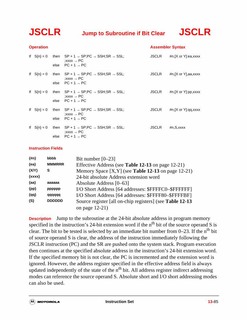
cution word. rd is ays
modes
JSCLR Jump to Subroutine if Bit Clear JSCLR
Instruction Fields
Description Jump to the subroutine at the 24-bit absolute address in program memory specified in the instruction’s 24-bit extension word if the nth bit of the source operand S isclear. The bit to be tested is selected by an immediate bit number from 0–23. If the nth bit of source operand S is clear, the address of the instruction immediately following theJSCLR instruction (PC) and the SR are pushed onto the system stack. Program exethen continues at the specified absolute address in the instruction’s 24-bit extensionIf the specified memory bit is not clear, the PC is incremented and the extension woignored. However, the address register specified in the effective address field is alwupdated independently of the state of the nth bit. All address register indirect addressing modes can reference the source operand S. Absolute short and I/O short addressingcan also be used.
Operation Assembler Syntax
If Sn = 0 then SP + 1 → SP;PC → SSH;SR → SSL;;xxxx → PC
JSCLR #n,[X or Y]:ea,xxxx
else PC + 1 → PC
If Sn = 0 then SP + 1 → SP;PC → SSH;SR → SSL;;xxxx → PC
JSCLR #n,[X or Y],aa,xxxx
else PC + 1 → PC
If Sn = 0 then SP + 1 → SP;PC → SSH;SR → SSL;;xxxx → PC
JSCLR #n,[X or Y]:pp,xxxx
else PC + 1 → PC
If Sn = 0 then SP + 1 → SP;PC → SSH;SR → SSL;;xxxx → PC
JSCLR #n,[X or Y]:qq,xxxx
else PC + 1 → PC
If Sn = 0 then SP + 1 → SP;PC → SSH;SR → SSL;;xxxx → PC
JSCLR #n,S,xxxx
else PC + 1 → PC
#n bbbb Bit number [0–23]ea MMMRRR Effective Address (see Table 12-13 on page 12-21)X/Y S Memory Space [X,Y] (see Table 12-13 on page 12-21)xxxx 24-bit absolute Address extension wordaa aaaaaa Absolute Address [0–63]pp pppppp I/O Short Address [64 addresses: $FFFFC0–$FFFFFF]qq qqqqqq I/O Short Address [64 addresses: $FFFF80–$FFFFBF]S DDDDDD Source register [all on-chip registers] (see Table 12-13
on page 12-21)
Instruction Set 13-85
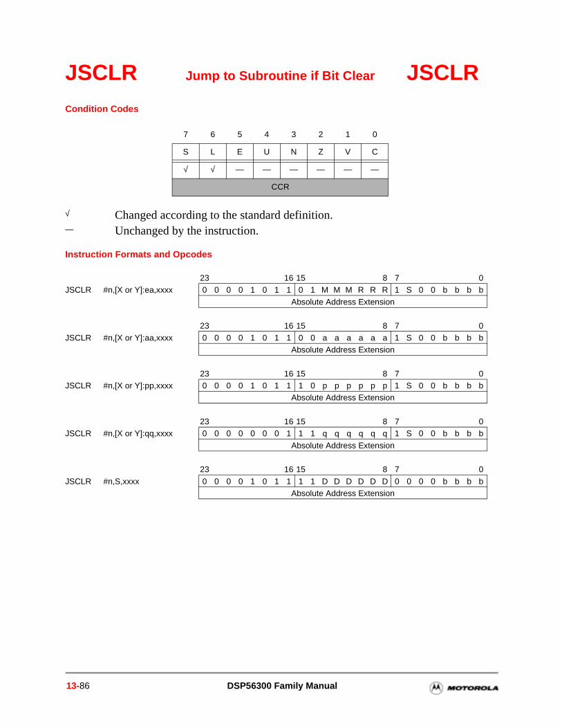
JSCLR Jump to Subroutine if Bit Clear JSCLRCondition Codes
Instruction Formats and Opcodes
7 6 5 4 3 2 1 0
S L E U N Z V C
√ √ — — — — — —
CCR
√ Changed according to the standard definition.— Unchanged by the instruction.
23 16 15 8 7 0JSCLR #n,[X or Y]:ea,xxxx 0 0 0 0 1 0 1 1 0 1 M M M R R R 1 S 0 0 b b b b
Absolute Address Extension
23 16 15 8 7 0
JSCLR #n,[X or Y]:aa,xxxx 0 0 0 0 1 0 1 1 0 0 a a a a a a 1 S 0 0 b b b bAbsolute Address Extension
23 16 15 8 7 0JSCLR #n,[X or Y]:pp,xxxx 0 0 0 0 1 0 1 1 1 0 p p p p p p 1 S 0 0 b b b b
Absolute Address Extension
23 16 15 8 7 0JSCLR #n,[X or Y]:qq,xxxx 0 0 0 0 0 0 0 1 1 1 q q q q q q 1 S 0 0 b b b b
Absolute Address Extension
23 16 15 8 7 0
JSCLR #n,S,xxxx 0 0 0 0 1 0 1 1 1 1 D D D D D D 0 0 0 0 b b b bAbsolute Address Extension
13-86 DSP56300 Family Manual
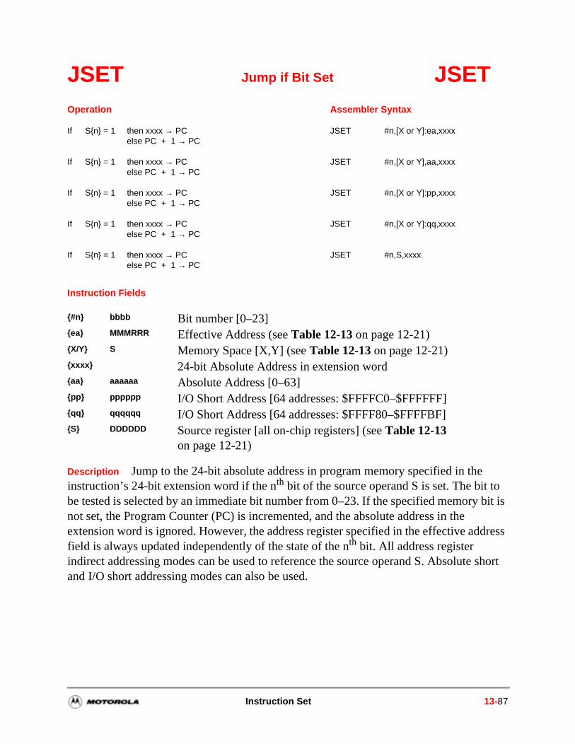
o bit is
dress
short
JSET Jump if Bit Set JSET
Instruction Fields
Description Jump to the 24-bit absolute address in program memory specified in the instruction’s 24-bit extension word if the nth bit of the source operand S is set. The bit tbe tested is selected by an immediate bit number from 0–23. If the specified memorynot set, the Program Counter (PC) is incremented, and the absolute address in the extension word is ignored. However, the address register specified in the effective adfield is always updated independently of the state of the nth bit. All address register indirect addressing modes can be used to reference the source operand S. Absoluteand I/O short addressing modes can also be used.
Operation Assembler Syntax
If Sn = 1 then xxxx → PC JSET #n,[X or Y]:ea,xxxxelse PC + 1 → PC
If Sn = 1 then xxxx → PC JSET #n,[X or Y],aa,xxxxelse PC + 1 → PC
If Sn = 1 then xxxx → PC JSET #n,[X or Y]:pp,xxxxelse PC + 1 → PC
If Sn = 1 then xxxx → PC JSET #n,[X or Y]:qq,xxxxelse PC + 1 → PC
If Sn = 1 then xxxx → PC JSET #n,S,xxxxelse PC + 1 → PC
#n bbbb Bit number [0–23]ea MMMRRR Effective Address (see Table 12-13 on page 12-21)X/Y S Memory Space [X,Y] (see Table 12-13 on page 12-21)xxxx 24-bit Absolute Address in extension wordaa aaaaaa Absolute Address [0–63]pp pppppp I/O Short Address [64 addresses: $FFFFC0–$FFFFFF]qq qqqqqq I/O Short Address [64 addresses: $FFFF80–$FFFFBF]S DDDDDD Source register [all on-chip registers] (see Table 12-13
on page 12-21)
Instruction Set 13-87

JSET Jump if Bit Set JSETCondition Codes
Instruction Formats and Opcodes
7 6 5 4 3 2 1 0
S L E U N Z V C
√ √ — — — — — —
CCR
√ Changed according to the standard definition.— Unchanged by the instruction.
23 16 15 8 7 0JSET #n,[X or Y]:ea,xxxx 0 0 0 0 1 0 1 0 0 1 M M M R R R 1 S 1 0 b b b b
Absolute Address Extension
23 16 15 8 7 0JSET #n,[X or Y]:aa,xxxx 0 0 0 0 1 0 1 0 0 0 a a a a a a 1 S 1 0 b b b b
Absolute Address Extension
23 16 15 8 7 0
JSET #n,[X or Y]:pp,xxxx 0 0 0 0 1 0 1 0 1 0 p p p p p p 1 S 1 0 b b b bAbsolute Address Extension
23 16 15 8 7 0JSET #n,[X or Y]:qq,xxxx 0 0 0 0 0 0 0 1 1 0 q q q q q q 1 S 1 0 b b b b
Absolute Address Extension
23 16 15 8 7 0JSET #n,S,xxxx 0 0 0 0 1 0 1 0 1 1 D D D D D D 0 0 1 0 b b b b
Absolute Address Extension
13-88 DSP56300 Family Manual
the stack. ory.
t short he
JSR Jump to Subroutine JSR
Instruction Fields
Description Jump to the subroutine whose location in program memory is given by the instruction’s effective address. The address of the instruction immediately following JSR instruction (PC) and the system Status Register (SR) is pushed onto the systemProgram execution then continues at the specified effective address in program memAll memory-alterable addressing modes can be used for the effective address. A fasjump addressing mode can also be used. The 12-bit data is zero-extended to form teffective address.
Condition Codes
Instruction Formats and Opcodes
Operation Assembler Syntax
SP + 1 → SP; PC → SSH; SR → SSL; 0xxx → PC JSR xxx
SP + 1 → SP; PC → SSH; SR → SSL; ea → PC JSR ea
xxx aaaaaaaaaaaa Short Jump Addressea MMMRRR Effective Address (see Table 12-13 on page 12-21)
7 6 5 4 3 2 1 0
S L E U N Z V C
— — — — — — — —
CCR
— Unchanged by the instruction.
23 16 15 8 7 0
JSR ea 0 0 0 0 1 0 1 1 1 1 M M M R R R 1 0 0 0 0 0 0 0Optional Effective Address Extension
23 16 15 8 7 0JSR xxx 0 0 0 0 1 1 0 1 0 0 0 0 a a a a a a a a a a a a
Instruction Set 13-89
stem
m ess e
JSSET Jump to Subroutine if Bit Set JSSET
Instruction Fields
Description Jump to the subroutine at the 24-bit absolute address in program memory specified in the instruction’s 24-bit extension word if the nth bit of the source operand S isset. The bit to be tested is selected by an immediate bit number from 0–23. If the nth bit of the source operand S is set, the address of the instruction immediately following theJSSET instruction (PC) and the system Status Register (SR) are pushed onto the systack. Program execution then continues at the specified absolute address in the instruction’s 24-bit extension word. If the specified memory bit is not set, the PrograCounter (PC) is incremented, and the extension word is ignored. However, the addrregister specified in the effective address field is always updated independently of th
Operation Assembler Syntax
If Sn = 1 then SP + 1 → SP;PC → SSH;SR → SSL;;xxxx → PC
JSSET #n,[X or Y]:ea,xxxx
else PC + 1 → PC
If Sn = 1 then SP + 1 → SP;PC → SSH;SR → SSL;;xxxx → PC
JSSET #n,[X or Y],aa,xxxx
else PC + 1 → PC
If Sn = 1 then SP + 1 → SP;PC → SSH;SR → SSL;;xxxx → PC
JSSET #n,[X or Y]:pp,xxxx
else PC + 1 → PC
If Sn = 1 then SP + 1 → SP;PC → SSH;SR → SSL;;xxxx → PC
JSSET #n,[X or Y]:qq,xxxx
else PC + 1 → PC
If Sn = 1 then SP + 1 → SP;PC → SSH;SR → SSL;;xxxx → PC
JSSET #n,S,xxxx
else PC + 1 → PC
#n bbbb Bit number [0–23]ea MMMRRR Effective Address (see Table 12-13 on page 12-21)X/Y S Memory Space [X,Y] (see Table 12-13 on page 12-21)xxxx 24-bit PC absolute Address extension wordaa aaaaaa Absolute Address [0–63]pp pppppp I/O Short Address [64 addresses: $FFFFC0–$FFFFFF]qq qqqqqq I/O Short Address [64 addresses: $FFFF80–$FFFFBF]S DDDDDD Source register [all on-chip registers] (see Table 12-13
on page 12-21)
13-90 DSP56300 Family Manual
JSSET Jump to Subroutine if Bit Set JSSET
state of the nth bit. All address register indirect addressing modes can be used to reference the source operand S. Absolute short and I/O short addressing modes can also be used.
Condition Codes
Instruction Formats and Opcodes
7 6 5 4 3 2 1 0
S L E U N Z V C
√ √ — — — — — —
CCR
√ Changed according to the standard definition.— Unchanged by the instruction.
23 16 15 8 7 0JSSET #n,[X or Y]:ea,xxxx 0 0 0 0 1 0 1 1 0 1 M M M R R R 1 S 1 0 b b b b
Absolute Address Extension
23 16 15 8 7 0
JSSET #n,[X or Y]:aa,xxxx 0 0 0 0 1 0 1 1 0 0 a a a a a a 1 S 1 0 b b b bAbsolute Address Extension
23 16 15 8 7 0JSSET #n,[X or Y]:pp,xxxx 0 0 0 0 1 0 1 1 1 0 p p p p p p 1 S 1 0 b b b b
Absolute Address Extension
23 16 15 8 7 0JSSET #n,[X or Y]:qq,xxxx 0 0 0 0 0 0 0 1 1 1 q q q q q q 1 S 1 0 b b b b
Absolute Address Extension
23 16 15 8 7 0
JSSET #n,S,xxxx 0 0 0 0 1 0 1 1 1 1 D D D D D D 0 0 1 0 b b b bAbsolute Address Extension
Instruction Set 13-91
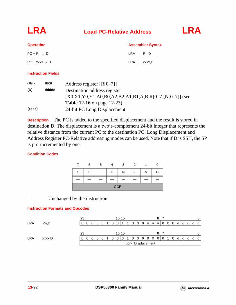
s the the SP
LRA Load PC-Relative Address LRA
Instruction Fields
Description The PC is added to the specified displacement and the result is stored in destination D. The displacement is a two’s-complement 24-bit integer that representrelative distance from the current PC to the destination PC. Long Displacement andAddress Register PC-Relative addressing modes can be used. Note that if D is SSH,is pre-incremented by one.
Condition Codes
Instruction Formats and Opcodes
Operation Assembler Syntax
PC + Rn → D LRA Rn,D
PC + xxxx → D LRA xxxx,D
Rn RRR Address register [R[0–7]]D ddddd Destination address register
[X0,X1,Y0,Y1,A0,B0,A2,B2,A1,B1,A,B,R[0–7],N[0–7]] (see Table 12-16 on page 12-23)
xxxx 24-bit PC Long Displacement
7 6 5 4 3 2 1 0
S L E U N Z V C
— — — — — — — —
CCR
— Unchanged by the instruction.
23 16 15 8 7 0LRA Rn,D 0 0 0 0 0 1 0 0 1 1 0 0 0 R R R 0 0 0 d d d d d
23 16 15 8 7 0LRA xxxx,D 0 0 0 0 0 1 0 0 0 1 0 0 0 0 0 0 0 1 0 d d d d d
Long Displacement
13-92 DSP56300 Family Manual
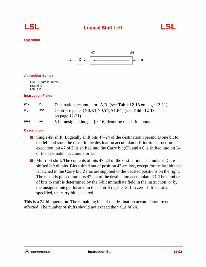
24
that ight. ber
y
LSL Logical Shift Left LSLOperation
Assembler Syntax
LSL D (parallel move)LSL #ii,DLSL S,D
Instruction Fields
Description
Single-bit shift: Logically shift bits 47–24 of the destination operand D one bit tothe left and store the result in the destination accumulator. Prior to instructionexecution, bit 47 of D is shifted into the Carry bit (C), and a 0 is shifted into bitof the destination accumulator D.
Multi-bit shift: The contents of bits 47–24 of the destination accumulator D areshifted left #ii bits. Bits shifted out of position 47 are lost, except for the last bit is latched in the Carry bit. Zeros are supplied to the vacated positions on the rThe result is placed into bits 47–24 of the destination accumulator D. The numof bits to shift is determined by the 5-bit immediate field in the instruction, or bthe unsigned integer located in the control register S. If a zero shift count is specified, the carry bit is cleared.
This is a 24-bit operation. The remaining bits of the destination accumulator are not affected. The number of shifts should not exceed the value of 24.
D D Destination accumulator [A,B] (see Table 12-13 on page 12-21)S sss Control register [X0,X1,Y0,Y1,A1,B1] (see Table 12-13
on page 12-21)#ii iiiii 5-bit unsigned integer [0–16] denoting the shift amount
0
2447
C
Instruction Set 13-93
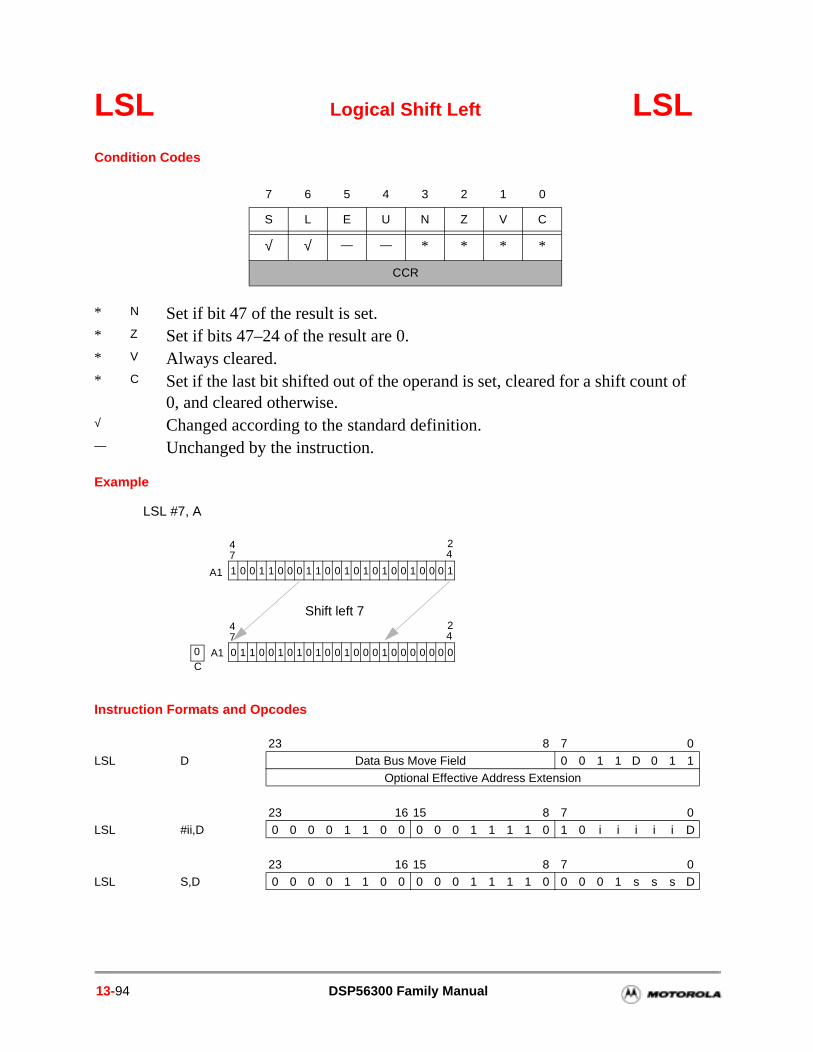
f
LSL Logical Shift Left LSLCondition Codes
Example
Instruction Formats and Opcodes
7 6 5 4 3 2 1 0
S L E U N Z V C
√ √ — — * * * *
CCR
* N Set if bit 47 of the result is set. * Z Set if bits 47–24 of the result are 0.* V Always cleared.* C Set if the last bit shifted out of the operand is set, cleared for a shift count o
0, and cleared otherwise. √ Changed according to the standard definition.— Unchanged by the instruction.
23 8 7 0LSL D Data Bus Move Field 0 0 1 1 D 0 1 1
Optional Effective Address Extension
23 16 15 8 7 0LSL #ii,D 0 0 0 0 1 1 0 0 0 0 0 1 1 1 1 0 1 0 i i i i i D
23 16 15 8 7 0LSL S,D 0 0 0 0 1 1 0 0 0 0 0 1 1 1 1 0 0 0 0 1 s s s D
LSL #7, A
A1 1 0 0 1 1 0 0 0 1 1 0 0 1 0 1 0 1 0 0 1 0 0 0 1
447
2
A1 0 1 1 0 0 1 0 1 0 1 0 0 1 0 0 0 1 0 0 0 0 0 0 0
447
2Shift left 7
0C
13-94 DSP56300 Family Manual
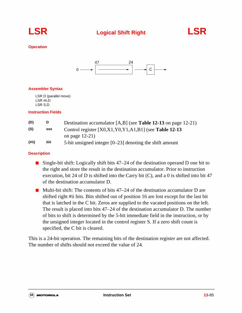
n 47
it left. ber
y
ted.
LSR Logical Shift Right LSROperation
Assembler Syntax
LSR D (parallel move)LSR #ii,DLSR S,D
Instruction Fields
Description
Single-bit shift: Logically shift bits 47–24 of the destination operand D one bit tothe right and store the result in the destination accumulator. Prior to instructioexecution, bit 24 of D is shifted into the Carry bit (C), and a 0 is shifted into bitof the destination accumulator D.
Multi-bit shift: The contents of bits 47–24 of the destination accumulator D areshifted right #ii bits. Bits shifted out of position 16 are lost except for the last bthat is latched in the C bit. Zeros are supplied to the vacated positions on the The result is placed into bits 47–24 of the destination accumulator D. The numof bits to shift is determined by the 5-bit immediate field in the instruction, or bthe unsigned integer located in the control register S. If a zero shift count is specified, the C bit is cleared.
This is a 24-bit operation. The remaining bits of the destination register are not affecThe number of shifts should not exceed the value of 24.
D D Destination accumulator [A,B] (see Table 12-13 on page 12-21)S sss Control register [X0,X1,Y0,Y1,A1,B1] (see Table 12-13
on page 12-21)#ii iiiii 5-bit unsigned integer [0–23] denoting the shift amount
0
24
C
47
Instruction Set 13-95
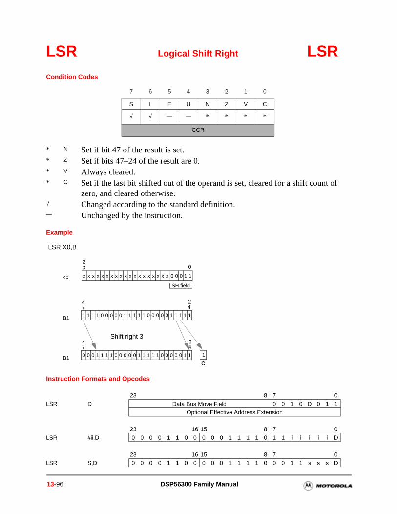
f
LSR Logical Shift Right LSRCondition Codes
Example
Instruction Formats and Opcodes
7 6 5 4 3 2 1 0
S L E U N Z V C
√ √ — — * * * *
CCR
* N Set if bit 47 of the result is set. * Z Set if bits 47–24 of the result are 0. * V Always cleared. * C Set if the last bit shifted out of the operand is set, cleared for a shift count o
zero, and cleared otherwise.√ Changed according to the standard definition.— Unchanged by the instruction.
23 8 7 0
LSR D Data Bus Move Field 0 0 1 0 D 0 1 1Optional Effective Address Extension
23 16 15 8 7 0LSR #ii,D 0 0 0 0 1 1 0 0 0 0 0 1 1 1 1 0 1 1 i i i i i D
23 16 15 8 7 0LSR S,D 0 0 0 0 1 1 0 0 0 0 0 1 1 1 1 0 0 0 1 1 s s s D
LSR X0,B
B1 1 1 1 1 0 0 0 0 0 1 1 1 1 1 0 0 0 0 0 1 1 1 1 1
447
2
B1 0 0 0 1 1 1 1 0 0 0 0 0 1 1 1 1 1 0 0 0 0 0 1 1
447
2
x x x x x x x x x x x x x x x x x x x 0 0 0 1 1
023
SH field
X0
1
c
Shift right 3
13-96 DSP56300 Family Manual
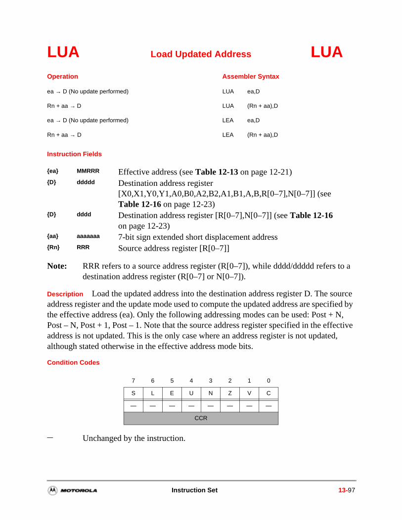
ource cified by N,
ffective ed,
LUA Load Updated Address LUA
Instruction Fields
Note: RRR refers to a source address register (R[0–7]), while dddd/ddddd refers to a destination address register (R[0–7] or N[0–7]).
Description Load the updated address into the destination address register D. The saddress register and the update mode used to compute the updated address are spethe effective address (ea). Only the following addressing modes can be used: Post +Post – N, Post + 1, Post – 1. Note that the source address register specified in the eaddress is not updated. This is the only case where an address register is not updatalthough stated otherwise in the effective address mode bits.
Condition Codes
Operation Assembler Syntax
ea → D (No update performed) LUA ea,D
Rn + aa → D LUA (Rn + aa),D
ea → D (No update performed) LEA ea,D
Rn + aa → D LEA (Rn + aa),D
ea MMRRR Effective address (see Table 12-13 on page 12-21)D ddddd Destination address register
[X0,X1,Y0,Y1,A0,B0,A2,B2,A1,B1,A,B,R[0–7],N[0–7]] (see Table 12-16 on page 12-23)
D dddd Destination address register [R[0–7],N[0–7]] (see Table 12-16 on page 12-23)
aa aaaaaaa 7-bit sign extended short displacement addressRn RRR Source address register [R[0–7]]
7 6 5 4 3 2 1 0
S L E U N Z V C
— — — — — — — —
CCR
— Unchanged by the instruction.
Instruction Set 13-97
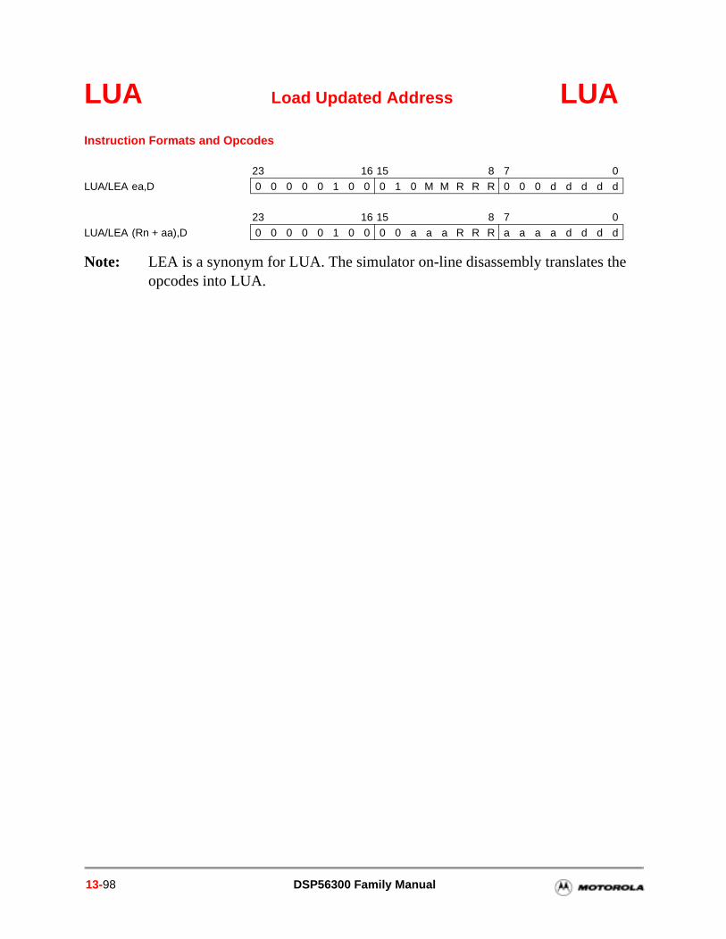
LUA Load Updated Address LUAInstruction Formats and Opcodes
Note: LEA is a synonym for LUA. The simulator on-line disassembly translates the opcodes into LUA.
23 16 15 8 7 0
LUA/LEA ea,D 0 0 0 0 0 1 0 0 0 1 0 M M R R R 0 0 0 d d d d d
23 16 15 8 7 0
LUA/LEA (Rn + aa),D 0 0 0 0 0 1 0 0 0 0 a a a R R R a a a a d d d d
13-98 DSP56300 Family Manual
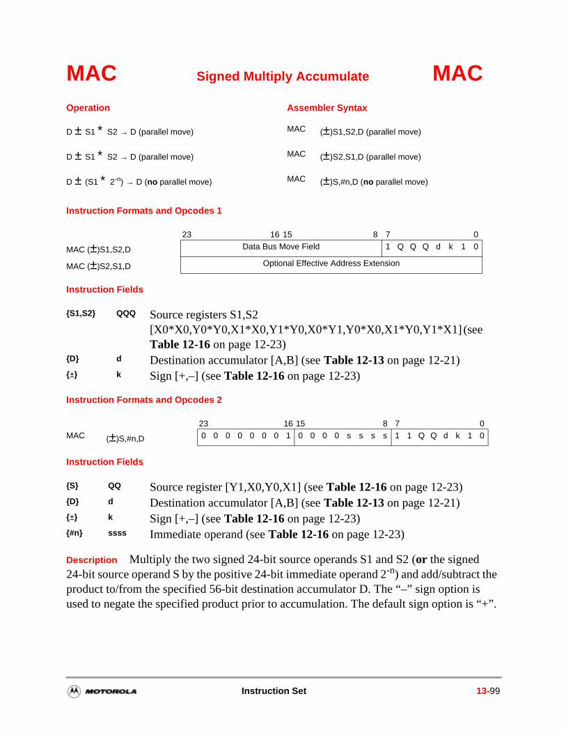
s “+”.
MAC Signed Multiply Accumulate MAC
Instruction Formats and Opcodes 1
Instruction Fields
Instruction Formats and Opcodes 2
Instruction Fields
Description Multiply the two signed 24-bit source operands S1 and S2 (or the signed 24-bit source operand S by the positive 24-bit immediate operand 2-n) and add/subtract the product to/from the specified 56-bit destination accumulator D. The “–” sign option isused to negate the specified product prior to accumulation. The default sign option i
Operation Assembler Syntax
D ± S1 ∗ S2 → D (parallel move) MAC (±)S1,S2,D (parallel move)
D ± S1 ∗ S2 → D (parallel move) MAC (±)S2,S1,D (parallel move)
D ± (S1 ∗ 2-n) → D (no parallel move) MAC (±)S,#n,D (no parallel move)
23 16 15 8 7 0
MAC (±)S1,S2,D Data Bus Move Field 1 Q Q Q d k 1 0
MAC (±)S2,S1,D Optional Effective Address Extension
S1,S2 QQQ Source registers S1,S2 [X0*X0,Y0*Y0,X1*X0,Y1*Y0,X0*Y1,Y0*X0,X1*Y0,Y1*X1] (see Table 12-16 on page 12-23)
D d Destination accumulator [A,B] (see Table 12-13 on page 12-21)± k Sign [+,–] (see Table 12-16 on page 12-23)
23 16 15 8 7 0MAC (±)S,#n,D 0 0 0 0 0 0 0 1 0 0 0 0 s s s s 1 1 Q Q d k 1 0
S QQ Source register [Y1,X0,Y0,X1] (see Table 12-16 on page 12-23)D d Destination accumulator [A,B] (see Table 12-13 on page 12-21)± k Sign [+,–] (see Table 12-16 on page 12-23)#n ssss Immediate operand (see Table 12-16 on page 12-23)
Instruction Set 13-99
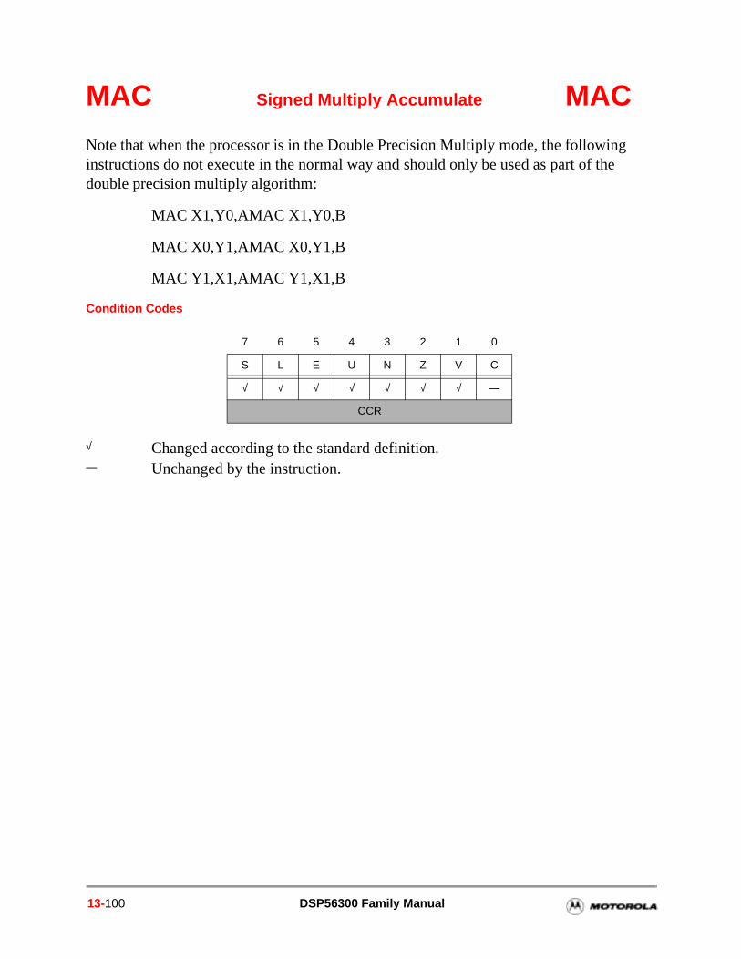
MAC Signed Multiply Accumulate MAC
Note that when the processor is in the Double Precision Multiply mode, the following instructions do not execute in the normal way and should only be used as part of the double precision multiply algorithm:
MAC X1,Y0,AMAC X1,Y0,B
MAC X0,Y1,AMAC X0,Y1,B
MAC Y1,X1,AMAC Y1,X1,B
Condition Codes
7 6 5 4 3 2 1 0
S L E U N Z V C
√ √ √ √ √ √ √ —
CCR
√ Changed according to the standard definition. — Unchanged by the instruction.
13-100 DSP56300 Family Manual
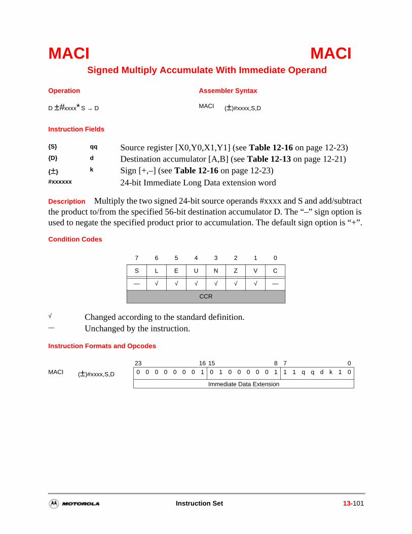
n is s “+”.
MACI MACI Signed Multiply Accumulate With Immediate Operand
Instruction Fields
Description Multiply the two signed 24-bit source operands #xxxx and S and add/subtract the product to/from the specified 56-bit destination accumulator D. The “–” sign optioused to negate the specified product prior to accumulation. The default sign option i
Condition Codes
Instruction Formats and Opcodes
Operation Assembler Syntax
D ±#xxxx∗S → D MACI (±)#xxxx,S,D
S qq Source register [X0,Y0,X1,Y1] (see Table 12-16 on page 12-23)D d Destination accumulator [A,B] (see Table 12-13 on page 12-21)± k Sign [+,–] (see Table 12-16 on page 12-23)#xxxxxx 24-bit Immediate Long Data extension word
7 6 5 4 3 2 1 0
S L E U N Z V C
— √ √ √ √ √ √ —
CCR
√ Changed according to the standard definition.— Unchanged by the instruction.
23 16 15 8 7 0MACI (±)#xxxx,S,D 0 0 0 0 0 0 0 1 0 1 0 0 0 0 0 1 1 1 q q d k 1 0
Immediate Data Extension
Instruction Set 13-101
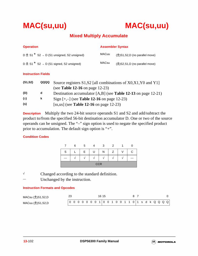
ct
MAC(su,uu) MAC(su,uu)Mixed Multiply Accumulate
Instruction Fields
Description Multiply the two 24-bit source operands S1 and S2 and add/subtract the product to/from the specified 56-bit destination accumulator D. One or two of the source operands can be unsigned. The “–” sign option is used to negate the specified produprior to accumulation. The default sign option is “+”.
Condition Codes
Instruction Formats and Opcodes
Operation Assembler Syntax
D ± S1 ∗ S2 → D (S1 unsigned, S2 unsigned) MACuu (±)S1,S2,D (no parallel move)
D ± S1 ∗ S2 → D (S1 signed, S2 unsigned) MACsu (±)S2,S1,D (no parallel move)
S1,S2 QQQQ Source registers S1,S2 [all combinations of X0,X1,Y0 and Y1](see Table 12-16 on page 12-23)
D d Destination accumulator [A,B] (see Table 12-13 on page 12-21)± k Sign [+,–] (see Table 12-16 on page 12-23)s [ss,us] (see Table 12-16 on page 12-23)
7 6 5 4 3 2 1 0
S L E U N Z V C
— √ √ √ √ √ √ —
CCR
√ Changed according to the standard definition. — Unchanged by the instruction.
MACsu (±)S1,S2,D 23 16 15 8 7 0
MACuu (±)S1,S2,D 0 0 0 0 0 0 0 1 0 0 1 0 0 1 1 0 1 s d k Q Q Q Q
13-102 DSP56300 Family Manual

e of
MACR Signed Multiply Accumulate and Round MACR
Instruction Formats and Opcodes 1
Instruction Fields
Instruction Formats and Opcodes 2
Instruction Fields
Description Multiply the two signed 24-bit source operands S1 and S2 (or the signed 24-bit source operand S by the positive 24-bit immediate operand 2-n), add/subtract the product to/from the specified 56-bit destination accumulator D, and round the result using either convergent or two’s-complement rounding. The rounded result is stored in destination accumulator D. The “–” sign option negates the specified product prior toaccumulation. The default sign option is “+.” The LSB of the result is rounded into thupper portion of the destination accumulator. Once rounding is complete, the LSBs
Operation Assembler Syntax
D ± S1 ∗ S2 + r → D (parallel move) MACR (±)S1,S2,D (parallel move)
D ± S1 ∗ S2 + r → D (parallel move) MACR (±)S2,S1,D (parallel move)
D ± (S1 ∗ 2-n) + r → D (no parallel move) MACR (±)S,#n,D (no parallel move)
23 16 15 8 7 0
MACR (±)S1,S2,D Data Bus Move Field 1 Q Q Q d k 1 1
MACR (±)S2,S1,D Optional Effective Address Extension
S1,S2 QQQ Source registers S1,S2 [X0*X0,Y0*Y0,X1*X0,Y1*Y0,X0*Y1,Y0*X0,X1*Y0,Y1*X1] (see Table 12-16 on page 12-23)
D d Destination accumulator [A,B] (see Table 12-13 on page 12-21)± k Sign [+,–] (see Table 12-16 on page 12-23)
23 16 15 8 7 0MACR (±)S,#n,D 0 0 0 0 0 0 0 1 0 0 0 0 3 s s s 1 1 Q Q d k 1 1
S QQ Source register [Y1,X0,Y0,X1] (see Table 12-16 on page 12-23)D d Destination accumulator [A,B] (see Table 12-13 on page 12-21)± k Sign [+,–] (see Table 12-16 on page 12-23)#n ssss Immediate operand (see Table 12-16 on page 12-23)
Instruction Set 13-103
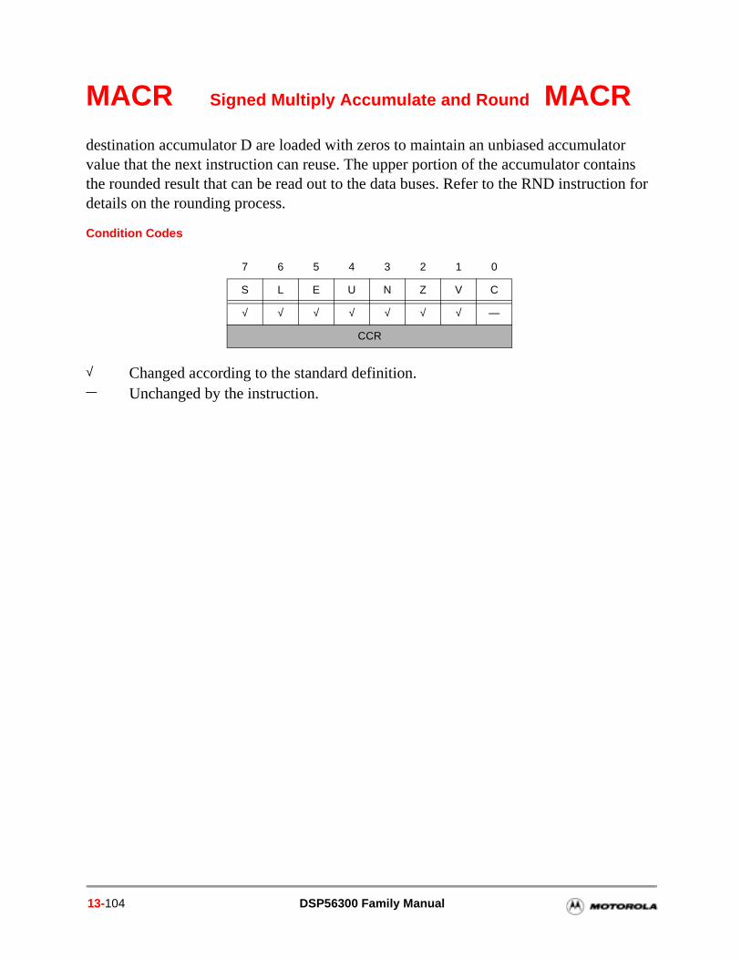
MACR Signed Multiply Accumulate and Round MACR
destination accumulator D are loaded with zeros to maintain an unbiased accumulator value that the next instruction can reuse. The upper portion of the accumulator contains the rounded result that can be read out to the data buses. Refer to the RND instruction for details on the rounding process.
Condition Codes
7 6 5 4 3 2 1 0
S L E U N Z V C
√ √ √ √ √ √ √ —
CCR
√ Changed according to the standard definition.— Unchanged by the instruction.
13-104 DSP56300 Family Manual
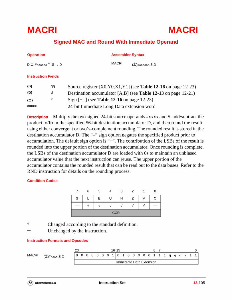
in the lt is plete, ed
r to the
MACRI MACRISigned MAC and Round With Immediate Operand
Instruction Fields
Description Multiply the two signed 24-bit source operands #xxxx and S, add/subtract the product to/from the specified 56-bit destination accumulator D, and then round the result using either convergent or two’s-complement rounding. The rounded result is stored destination accumulator D. The “–” sign option negates the specified product prior toaccumulation. The default sign option is “+”. The contribution of the LSBs of the resurounded into the upper portion of the destination accumulator. Once rounding is comthe LSBs of the destination accumulator D are loaded with 0s to maintain an unbiasaccumulator value that the next instruction can reuse. The upper portion of the accumulator contains the rounded result that can be read out to the data buses. RefeRND instruction for details on the rounding process.
Condition Codes
Instruction Formats and Opcodes
Operation Assembler Syntax
D ± #xxxxxx ∗ S → D MACRI (±)#xxxxxx,S,D
S qq Source register [X0,Y0,X1,Y1] (see Table 12-16 on page 12-23)D d Destination accumulator [A,B] (see Table 12-13 on page 12-21)± k Sign [+,-] (see Table 12-16 on page 12-23)#xxxx 24-bit Immediate Long Data extension word
7 6 5 4 3 2 1 0
S L E U N Z V C
— √ √ √ √ √ √ —
CCR
√ Changed according to the standard definition.— Unchanged by the instruction.
23 16 15 8 7 0
MACRI (±)#xxxx,S,D 0 0 0 0 0 0 0 1 0 1 0 0 0 0 0 1 1 1 q q d k 1 1
Immediate Data Extension
Instruction Set 13-105
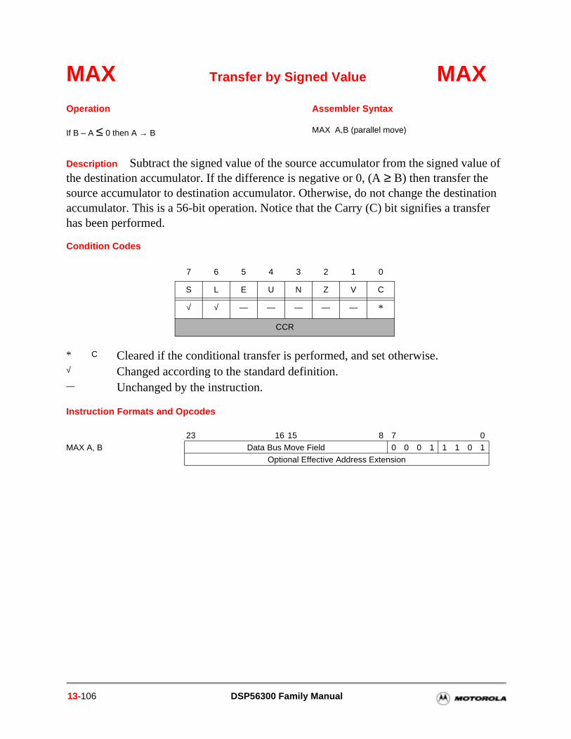
MAX Transfer by Signed Value MAX
Description Subtract the signed value of the source accumulator from the signed value of the destination accumulator. If the difference is negative or 0, (A ≥ B) then transfer the source accumulator to destination accumulator. Otherwise, do not change the destination accumulator. This is a 56-bit operation. Notice that the Carry (C) bit signifies a transfer has been performed.
Condition Codes
Instruction Formats and Opcodes
Operation Assembler Syntax
If B – A ≤ 0 then A → B MAX A,B (parallel move)
7 6 5 4 3 2 1 0
S L E U N Z V C
√ √ — — — — — *
CCR
* C Cleared if the conditional transfer is performed, and set otherwise.√ Changed according to the standard definition.— Unchanged by the instruction.
23 16 15 8 7 0MAX A, B Data Bus Move Field 0 0 0 1 1 1 0 1
Optional Effective Address Extension
13-106 DSP56300 Family Manual
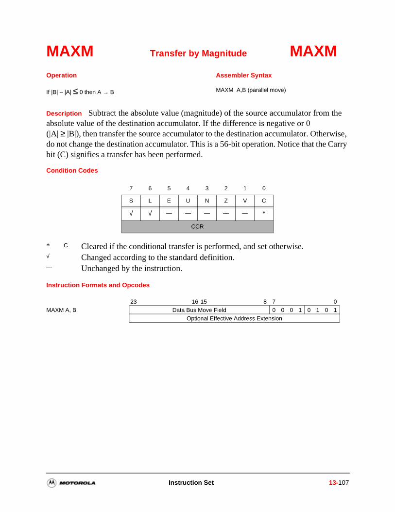
MAXM Transfer by Magnitude MAXM
Description Subtract the absolute value (magnitude) of the source accumulator from the absolute value of the destination accumulator. If the difference is negative or 0 (|A| ≥ |B|), then transfer the source accumulator to the destination accumulator. Otherwise, do not change the destination accumulator. This is a 56-bit operation. Notice that the Carry bit (C) signifies a transfer has been performed.
Condition Codes
Instruction Formats and Opcodes
Operation Assembler Syntax
If |B| – |A| ≤ 0 then A → B MAXM A,B (parallel move)
7 6 5 4 3 2 1 0
S L E U N Z V C
√ √ — — — — — *
CCR
* C Cleared if the conditional transfer is performed, and set otherwise.√ Changed according to the standard definition. — Unchanged by the instruction.
23 16 15 8 7 0MAXM A, B Data Bus Move Field 0 0 0 1 0 1 0 1
Optional Effective Address Extension
Instruction Set 13-107
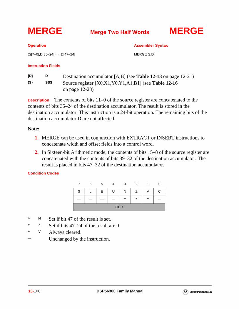
the
r are he
MERGE Merge Two Half Words MERGE
Instruction Fields
Description The contents of bits 11–0 of the source register are concatenated to the contents of bits 35–24 of the destination accumulator. The result is stored in the destination accumulator. This instruction is a 24-bit operation. The remaining bits ofdestination accumulator D are not affected.
Note:
1. MERGE can be used in conjunction with EXTRACT or INSERT instructions toconcatenate width and offset fields into a control word.
2. In Sixteen-bit Arithmetic mode, the contents of bits 15–8 of the source registeconcatenated with the contents of bits 39–32 of the destination accumulator. Tresult is placed in bits 47–32 of the destination accumulator.
Condition Codes
Operation Assembler Syntax
S[7–0],D[35–24] → D[47–24] MERGE S,D
D D Destination accumulator [A,B] (see Table 12-13 on page 12-21)S SSS Source register [X0,X1,Y0,Y1,A1,B1] (see Table 12-16
on page 12-23)
7 6 5 4 3 2 1 0
S L E U N Z V C
— — — — * * * —
CCR
* N Set if bit 47 of the result is set. * Z Set if bits 47–24 of the result are 0. * V Always cleared. — Unchanged by the instruction.
13-108 DSP56300 Family Manual
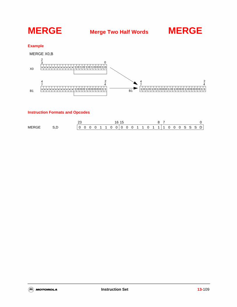
MERGE Merge Two Half Words MERGEExample
Instruction Formats and Opcodes
23 16 15 8 7 0
MERGE S,D 0 0 0 0 1 1 0 0 0 0 0 1 1 0 1 1 1 0 0 0 S S S D
MERGE X0,B
X0 x x x x x x x x x x x x 1 0 1 0 1 0 1 0 0 0 1 0
023
B1 x x x x x x x x x x x x 1 0 0 0 1 0 0 0 0 0 1 1
447
2
B1 1 0 1 0 1 0 1 0 0 0 1 0 1 0 0 0 1 0 0 0 0 0 1 1
447
2
Instruction Set 13-109
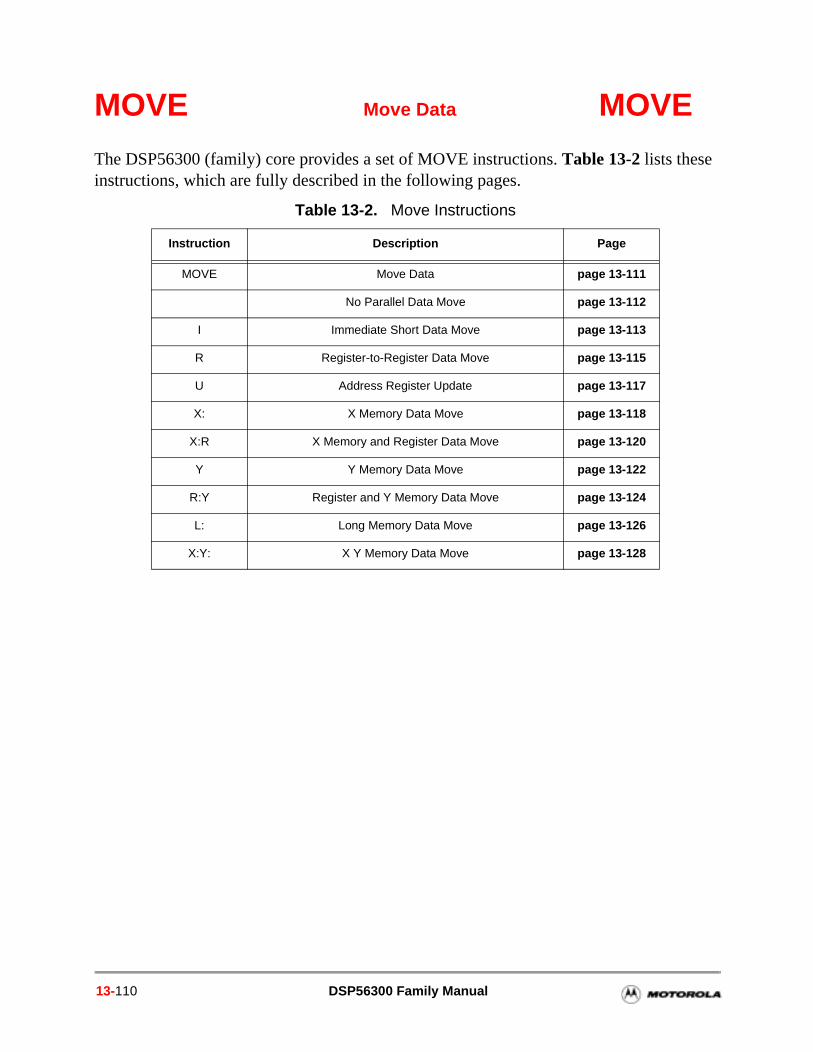
MOVE Move Data MOVE
The DSP56300 (family) core provides a set of MOVE instructions. Table 13-2 lists these instructions, which are fully described in the following pages.
Table 13-2. Move Instructions
Instruction Description Page
MOVE Move Data page 13-111
No Parallel Data Move page 13-112
I Immediate Short Data Move page 13-113
R Register-to-Register Data Move page 13-115
U Address Register Update page 13-117
X: X Memory Data Move page 13-118
X:R X Memory and Register Data Move page 13-120
Y Y Memory Data Move page 13-122
R:Y Register and Y Memory Data Move page 13-124
L: Long Memory Data Move page 13-126
X:Y: X Y Memory Data Move page 13-128
13-110 DSP56300 Family Manual
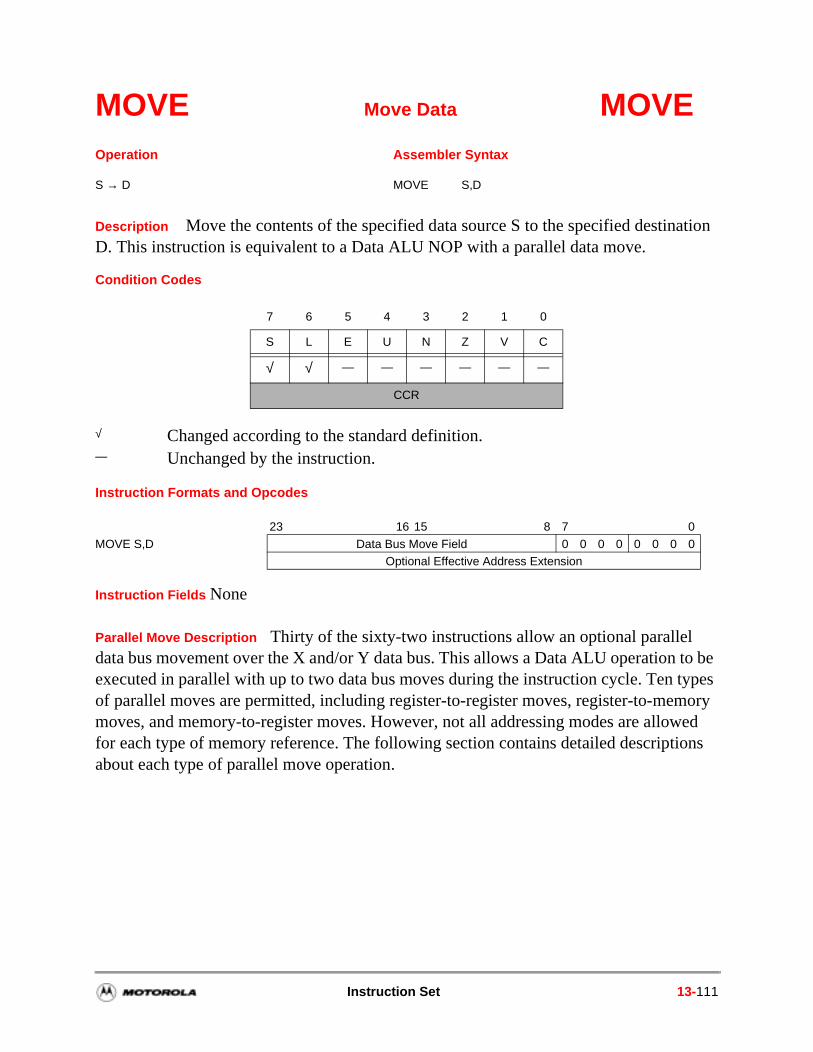
MOVE Move Data MOVE
Description Move the contents of the specified data source S to the specified destination D. This instruction is equivalent to a Data ALU NOP with a parallel data move.
Condition Codes
Instruction Formats and Opcodes
Instruction Fields None
Parallel Move Description Thirty of the sixty-two instructions allow an optional parallel data bus movement over the X and/or Y data bus. This allows a Data ALU operation to be executed in parallel with up to two data bus moves during the instruction cycle. Ten types of parallel moves are permitted, including register-to-register moves, register-to-memory moves, and memory-to-register moves. However, not all addressing modes are allowed for each type of memory reference. The following section contains detailed descriptions about each type of parallel move operation.
Operation Assembler Syntax
S → D MOVE S,D
7 6 5 4 3 2 1 0
S L E U N Z V C
√ √ — — — — — —
CCR
√ Changed according to the standard definition. — Unchanged by the instruction.
23 16 15 8 7 0
MOVE S,D Data Bus Move Field 0 0 0 0 0 0 0 0Optional Effective Address Extension
Instruction Set 13-111
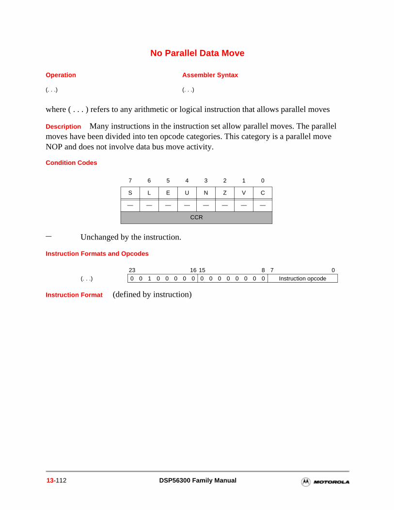
No Parallel Data Move
where ( . . . ) refers to any arithmetic or logical instruction that allows parallel moves
Description Many instructions in the instruction set allow parallel moves. The parallel moves have been divided into ten opcode categories. This category is a parallel move NOP and does not involve data bus move activity.
Condition Codes
Instruction Formats and Opcodes
Instruction Format (defined by instruction)
Operation Assembler Syntax
(. . .) (. . .)
7 6 5 4 3 2 1 0
S L E U N Z V C
— — — — — — — —
CCR
— Unchanged by the instruction.
23 16 15 8 7 0(. . .) 0 0 1 0 0 0 0 0 0 0 0 0 0 0 0 0 Instruction opcode
13-112 DSP56300 Family Manual
ion nation as a ta is
ot be
A1, on ion of
I Immediate Short Data Move I
where ( . . . ) refers to any arithmetic or logical instruction that allows parallel moves
Instruction Fields
Description Move the 8-bit immediate data value (#xx) into the destination operand D. If the destination register D is A0, A1, A2, B0, B1, B2, R[0–7], or N]0–7], the 8-bit immediate short operand is interpreted as an unsigned integer and is stored in the specifieddestination register. That is, the 8-bit data is stored in the eight LSBs of the destinatoperand and the remaining bits of the destination operand D are zeroed. If the destiregister D is X0, X1, Y0, Y1, A, or B, the 8-bit immediate short operand is interpretedsigned fraction and is stored in the specified destination register. That is, the 8-bit dastored in the eight MSBs of the destination operand and the remaining bits of the destination operand D are zeroed.
If the arithmetic or logical opcode-operand portion of the instruction specifies a givendestination accumulator, that same accumulator or portion of that accumulator cannspecified as a destination D in the parallel data bus move operation. Thus, if the opcode-operand portion of the instruction specifies the 56-bit A accumulator as its destination, the parallel data bus move portion of the instruction cannot specify A0, A2, or A as its destination D. Similarly, if the opcode-operand portion of the instructispecifies the 56-bit B accumulator as its destination, the parallel data bus move portthe instruction cannot specify B0, B1, B2, or B as its destination D. That is, duplicatedestinations are not allowed within the same instruction.
Condition Codes
Operation Assembler Syntax
( . . . ), #xx → D ( . . . ) #xx,D
#xx iiiiiiii 8-bit Immediate Short DataD ddddd Destination register
[X0,X1,Y0,Y1,A0,B0,A2,B2,A1,B1,A,B,R[0 – 7],N[0–7]] (see Table 12-13 on page 12-21)
7 6 5 4 3 2 1 0
S L E U N Z V C
— — — — — — — —
CCR
— Unchanged by the instruction.
Instruction Set 13-113
I Immediate Short Data Move IInstruction Formats and Opcodes
23 16 15 8 7 0
( . . . ) #xx,D 0 0 1 d d d d d i i i i i i i i Instruction opcode
13-114 DSP56300 Family Manual
R Register-to-Register Data Move R
where ( . . . ) refers to any arithmetic or logical instruction that allows parallel moves.
Instruction Fields
Description Move the source register S to the destination register D. If the arithmetic or logical opcode-operand portion of the instruction specifies a given destination accumulator, that same accumulator or portion of that accumulator cannot be specified as a destination D in the parallel data bus move operation. Thus, if the opcode-operand portion of the instruction specifies the 56-bit A accumulator as its destination, the parallel data bus move portion of the instruction cannot specify A0, A1, A2, or A as its destination D. Similarly, if the opcode-operand portion of the instruction specifies the 56-bit B accumulator as its destination, the parallel data bus move portion of the instruction cannot specify B0, B1, B2, or B as its destination D. That is, duplicate destinations are not allowed within the same instruction.
If the opcode-operand portion of the instruction specifies a given source or destination register, that same register or portion of that register can be used as a source S in the parallel data bus move operation. This allows data to be moved in the same instruction in which a Data ALU operation is using it as a source operand. That is, duplicate sources are allowed within the same instruction. Note that the MOVE A,B operation results in a 24-bit positive or negative saturation constant being stored in the B1 portion of the B accumulator if the signed integer portion of the A accumulator is in use.
Operation Assembler Syntax
( . . . ); S → D ( . . . ) S,D
S eeeee Source register [X0,X1,Y0,Y1,A0,B0,A2,B2,A1,B1,A,B,R[0–7],N[0 – 7] (see Table 12-16 on page 12-23)
D ddddd Destination register [X0,X1,Y0,Y1,A0,B0,A2,B2,A1,B1,A,B,R[0 – 7],N[0–7]] (see Table 12-13 on page 12-21)
Instruction Set 13-115

R Register-to-Register Data Move RCondition Codes
Instruction Formats and Opcodes
7 6 5 4 3 2 1 0
S L E U N Z V C
√ √ — — — — — —
CCR
√ Changed according to the standard definition. — Unchanged by the instruction.
23 16 15 8 7 0( . . . ) S,D 0 0 1 0 0 0 e e e e e d d d d d Instruction opcode
13-116 DSP56300 Family Manual
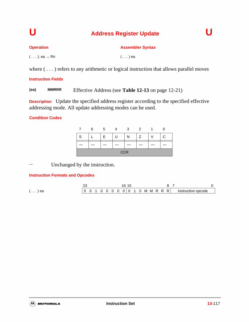
U Address Register Update U
where ( . . . ) refers to any arithmetic or logical instruction that allows parallel moves
Instruction Fields
Description Update the specified address register according to the specified effective addressing mode. All update addressing modes can be used.
Condition Codes
Instruction Formats and Opcodes
Operation Assembler Syntax
( . . . ); ea → Rn ( . . . ) ea
ea MMRRR Effective Address (see Table 12-13 on page 12-21)
7 6 5 4 3 2 1 0
S L E U N Z V C
— — — — — — — —
CCR
— Unchanged by the instruction.
23 16 15 8 7 0
( . . . ) ea 0 0 1 0 0 0 0 0 0 1 0 M M R R R Instruction opcode
Instruction Set 13-117
X: X Memory Data Move X:
where ( . . . ) refers to any arithmetic or logical instruction that allows parallel moves.
Instruction Formats and Opcodes 1
Instruction Fields
Instruction Formats and Opcodes 2
Operation Assembler Syntax
( . . . ); X:ea → D ( . . . ) X:ea,D
( . . . ); X:aa → D ( . . . ) X:aa,D
( . . . ); S → X:ea ( . . . ) S,X:ea
( . . . ); S → X:aa ( . . . ) S,X:aa
X:(Rn + xxx) → D MOVE X:(Rn + xxx),D
X:(Rn + xxxx) → D MOVE X:(Rn + xxxx),D
D → X:(Rn + xxx) MOVE D,X:(Rn + xxx)
D → X:(Rn + xxxx) MOVE D,X:(Rn + xxxx)
( . . . ) X:ea,D 23 16 15 8 7 0( . . . ) S,X:ea 0 1 d d 0 d d d W 1 M M M R R R Instruction opcode
( . . . ) #xxxxxx,D Optional Effective Address Extension
( . . . ) X:aa,D 23 16 15 8 7 0
( . . . ) S,X:aa 0 1 d d 0 d d d W 0 a a a a a a Instruction opcode
ea MMMRRR Effective Address (see Table 12-13 on page 12-21)W Read S / Write D bit (see Table 12-16 on page 12-23)
S,D ddddd Source/Destination registers [X0,X1,Y0,Y1,A0,B0,A2,B2,A1,B1,A,B,R[0–7],N[0 – 7]] (see Table 12-13 on page 12-21)
aa aaaaaa 6-bit Absolute Short Address
23 16 15 8 7 0
MOVE X:(Rn + xxxx),D 0 0 0 0 1 0 1 0 0 1 1 1 0 R R R 1 W D D D D D DMOVE S,X:(Rn + xxxx) Rn Relative Displacement
MOVE X:(Rn + xxx),D 23 16 15 8 7 0MOVE S,X:(Rn + xxx) 0 0 0 0 0 0 1 a a a a a a R R R 1 a 0 W D D D D
13-118 DSP56300 Family Manual
X: X Memory Data Move X:Instruction Fields
Description Move the specified word operand from/to X memory. All memory addressing modes can be used, including absolute addressing and 24-bit immediate data. Absolute short addressing can also be used. If the arithmetic or logical opcode-operand portion of the instruction specifies a given destination accumulator, that same accumulator or portion of that accumulator cannot be specified as a destination D in the parallel data bus move operation. Thus, if the opcode-operand portion of the instruction specifies the 56-bit A accumulator as its destination, the parallel data bus move portion of the instruction cannot specify A0, A1, A2, or A as its destination D. Similarly, if the opcode-operand portion of the instruction specifies the 56-bit B accumulator as its destination, the parallel data bus move portion of the instruction cannot specify B0, B1, B2, or B as its destination D. That is, duplicate destinations are not allowed within the same instruction.
If the opcode-operand portion of the instruction specifies a given source or destination register, that same register or portion of that register can be used as a source S in the parallel data bus move operation. This allows data to be moved in the same instruction in which it is being used as a source operand by a Data ALU operation. That is, duplicate sources are allowed within the same instruction. As a result of the MOVE A,X:ea operation, a 24-bit positive or negative saturation constant is stored in the specified 24-bit X memory location if the signed integer portion of the A accumulator is in use.
Condition Codes
W Read S / Write D bit (see Table 12-16 on page 12-23)xxx aaaaaaa 7-bit sign extended Short Displacement AddressRn RRR Address register (R[0–7])D DDDD Source/Destination registers
[X0,X1,Y0,Y1,A0,B0,A2,B2,A1,B1,A,B] (see Table 12-16 on page 12-23)
S,D DDDDDD Source/Destination registers [all on-chip registers] (see Table 12-13 on page 12-21)
7 6 5 4 3 2 1 0
S L E U N Z V C
√ √ — — — — — —
CCR
√ Changed according to the standard definition. — Unchanged by the instruction.
Instruction Set 13-119
X:R X Memory and Register Data Move X:R
where ( . . . ) refers to any arithmetic or logical instruction that allows parallel moves
Class I Instruction Formats and Opcodes
Instruction Fields
Class II Instruction Formats and Opcodes
Instruction Fields
Operation Assembler Syntax
Class I( . . . ); X:ea → D1; S2 → D2 ( . . . ) X:ea,D1 S2,D2
( . . . ); S1 → X:ea; S2 → D2 ( . . . ) S1,X:ea S2,D2
( . . . ); #xxxxxx → D1; S2 → D2 ( . . . ) #xxxxxx,D1 S2,D2
Class II( . . . ); A → X:ea; X0 → A ( . . . ) A,X:ea X0,A
( . . . ); B → X:ea; X0 → B ( . . . ) B,X:ea X0,B
( . . . ) X:ea,D1 S2,D2 23 16 15 8 7 0
( . . . ) S1,X:ea S2, D2 0 0 0 1 f f d F W 0 M M M R R R Instruction opcode( . . . ) #xxxx,D1 S2,D2 Optional Effective Address Extension
ea MMMRRR Effective Address (see Table 12-13 on page 12-21)W Read S1/Write D1 bit (see Table 12-16 on page 12-23)
S1,D1 ff S1/D1 register [X0,X1,A,B] (see Table 12-16 on page 12-23)
S2 d S2 accumulator [A,B] (see Table 12-13 on page 12-21)D2 F D2 input register [Y0,Y1] (see Table 12-16 on page 12-23)
23 16 15 8 7 0( . . . ) A → X:ea X0 → A 0 0 0 0 1 0 0 d 0 0 M M M R R R Instruction opcode
( . . . ) B → X:ea X0 → B Optional Effective Address Extension
ea MMMRRR Effective Address (see Table 12-13 on page 12-21)d Move opcode (see Table 12-16 on page 12-23)
13-120 DSP56300 Family Manual
e
X:R X Memory and Register Data Move X:RDescription
Class I: Move a one-word operand from/to X memory and move another word operand from an accumulator (S2) to an input register (D2). All memory addressing modes, including absolute addressing and 24-bit immediate data, can be used. The register-to-register move (S2,D2) allows a Data ALU accumulator to be moved to a Data ALU input register for use as a Data ALU operand in the following instruction.
Class II: Move one-word operand from a Data ALU accumulator to X memory and one-word operand from Data ALU register X0 to a Data ALU accumulator. One effective address is specified. All memory addressing modes except long absolute addressing and long immediate data can be used.
For both Class I and Class II X:R parallel data moves, if the arithmetic or logical opcode-operand portion of the instruction specifies a given destination accumulator, that same accumulator or portion of that accumulator cannot be specified as a destination D1 in the parallel data bus move operation. Thus, if the opcode-operand portion of the instruction specifies the 40-bit A accumulator as its destination, the parallel data bus move portion of the instruction cannot specify A0, A1, A2, or A as its destination D1. Similarly, if the opcode-operand portion of the instruction specifies the 56-bit B accumulator as its destination, the parallel data bus move portion of the instruction cannot specify B0, B1, B2, or B as its destination D1. That is, duplicate destinations are not allowed within the same instruction. If the opcode-operand portion of the instruction specifies a given source or destination register, that same register or portion of that register can be used as a source S1 and/or S2 in the parallel data bus move operation. This allows data to be moved in the same instruction in which a Data ALU operation is using it as a source operand. That is, duplicate sources are allowed within the same instruction—S1 and S2 can specify thsame register.
Condition Codes
7 6 5 4 3 2 1 0
S L E U N Z V C
√ √ — — — — — —
CCR
√ Changed according to the standard definition.— Unchanged by the instruction.
Instruction Set 13-121
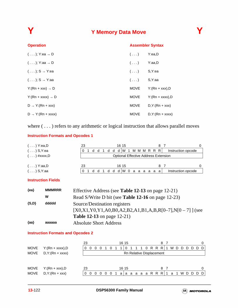
Y Y Memory Data Move Y
where ( . . . ) refers to any arithmetic or logical instruction that allows parallel moves
Instruction Formats and Opcodes 1
Instruction Fields
Instruction Formats and Opcodes 2
Operation Assembler Syntax
( . . . ); Y:ea → D ( . . . ) Y:ea,D
( . . . ); Y:aa → D ( . . . ) Y:aa,D
( . . . ); S → Y:ea ( . . . ) S,Y:ea
( . . . ); S → Y:aa ( . . . ) S,Y:aa
Y:(Rn + xxx) → D MOVE Y:(Rn + xxx),D
Y:(Rn + xxxx) → D MOVE Y:(Rn + xxxx),D
D → Y:(Rn + xxx) MOVE D,Y:(Rn + xxx)
D → Y:(Rn + xxxx) MOVE D,Y:(Rn + xxxx)
( . . . ) Y:ea,D 23 16 15 8 7 0( . . . ) S,Y:ea 0 1 d d 1 d d d W 1 M M M R R R Instruction opcode
( . . . ) #xxxx,D Optional Effective Address Extension
( . . . ) Y:aa,D 23 16 15 8 7 0
( . . . ) S,Y:aa 0 1 d d 1 d d d W 0 a a a a a a Instruction opcode
ea MMMRRR Effective Address (see Table 12-13 on page 12-21)W Read S/Write D bit (see Table 12-16 on page 12-23)
S,D ddddd Source/Destination registers [X0,X1,Y0,Y1,A0,B0,A2,B2,A1,B1,A,B,R[0–7],N[0 – 7] ] (see Table 12-13 on page 12-21)
aa aaaaaa Absolute Short Address
23 16 15 8 7 0
MOVE Y:(Rn + xxxx),D 0 0 0 0 1 0 1 1 0 1 1 1 0 R R R 1 W D D D D D DMOVE D,Y:(Rn + xxxx) Rn Relative Displacement
MOVE Y:(Rn + xxx),D 23 16 15 8 7 0MOVE D,Y:(Rn + xxx) 0 0 0 0 0 0 1 a a a a a a R R R 1 a 1 W D D D D
13-122 DSP56300 Family Manual
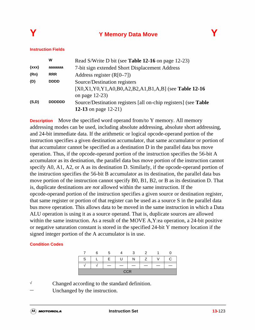
Y Y Memory Data Move YInstruction Fields
Description Move the specified word operand from/to Y memory. All memory addressing modes can be used, including absolute addressing, absolute short addressing, and 24-bit immediate data. If the arithmetic or logical opcode-operand portion of the instruction specifies a given destination accumulator, that same accumulator or portion of that accumulator cannot be specified as a destination D in the parallel data bus move operation. Thus, if the opcode-operand portion of the instruction specifies the 56-bit A accumulator as its destination, the parallel data bus move portion of the instruction cannot specify A0, A1, A2, or A as its destination D. Similarly, if the opcode-operand portion of the instruction specifies the 56-bit B accumulator as its destination, the parallel data bus move portion of the instruction cannot specify B0, B1, B2, or B as its destination D. That is, duplicate destinations are not allowed within the same instruction. If the opcode-operand portion of the instruction specifies a given source or destination register, that same register or portion of that register can be used as a source S in the parallel data bus move operation. This allows data to be moved in the same instruction in which a Data ALU operation is using it as a source operand. That is, duplicate sources are allowed within the same instruction. As a result of the MOVE A,Y:ea operation, a 24-bit positive or negative saturation constant is stored in the specified 24-bit Y memory location if the signed integer portion of the A accumulator is in use.
Condition Codes
W Read S/Write D bit (see Table 12-16 on page 12-23)xxx aaaaaaa 7-bit sign extended Short Displacement AddressRn RRR Address register (R[0–7])D DDDD Source/Destination registers
[X0,X1,Y0,Y1,A0,B0,A2,B2,A1,B1,A,B] (see Table 12-16 on page 12-23)
S,D DDDDDD Source/Destination registers [all on-chip registers] (see Table 12-13 on page 12-21)
7 6 5 4 3 2 1 0
S L E U N Z V C
√ √ — — — — — —
CCR
√ Changed according to the standard definition. — Unchanged by the instruction.
Instruction Set 13-123
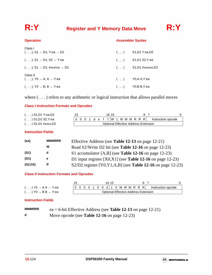
R:Y Register and Y Memory Data Move R:Y
where ( . . . ) refers to any arithmetic or logical instruction that allows parallel moves
Class I Instruction Formats and Opcodes
Instruction Fields
Class II Instruction Formats and Opcodes
Instruction Fields
Operation Assembler Syntax
Class I( . . . ); S1 → D1; Y:ea → D2 ( . . . ) S1,D1 Y:ea,D2
( . . . ); S1 → D1; S2 → Y:ea ( . . . ) S1,D1 S2,Y:ea
( . . . ); S1 → D1; #xxxxxx → D2 ( . . . ) S1,D1 #xxxxxx,D2
Class II( . . . ); Y0 → A; A → Y:ea ( . . . ) Y0,A A,Y:ea
( . . . ); Y0 → B; B → Y:ea ( . . . ) Y0,B B,Y:ea
( . . . ) S1,D1 Y:ea,D2 23 16 15 8 7 0
( . . . ) S1,D1 S2,Y:ea 0 0 0 1 d e f f W 1 M M M R R R Instruction opcode( . . . ) S1,D1 #xxxx,D2 Optional Effective Address Extension
ea MMMRRR Effective Address (see Table 12-13 on page 12-21)W Read S2/Write D2 bit (see Table 12-16 on page 12-23)
S1 d S1 accumulator [A,B] (see Table 12-16 on page 12-23)D1 e D1 input register [X0,X1] (see Table 12-16 on page 12-23)S2,D2 ff S2/D2 register [Y0,Y1,A,B] (see Table 12-16 on page 12-23)
23 16 15 8 7 0( . . . ) Y0 → A A → Y:ea 0 0 0 0 1 0 0 d 1 0 M M M R R R Instruction opcode( . . . ) Y0 → B B → Y:ea Optional Effective Address Extension
MMMRRR ea = 6-bit Effective Address (see Table 12-13 on page 12-21)d Move opcode (see Table 12-16 on page 12-23)
13-124 DSP56300 Family Manual
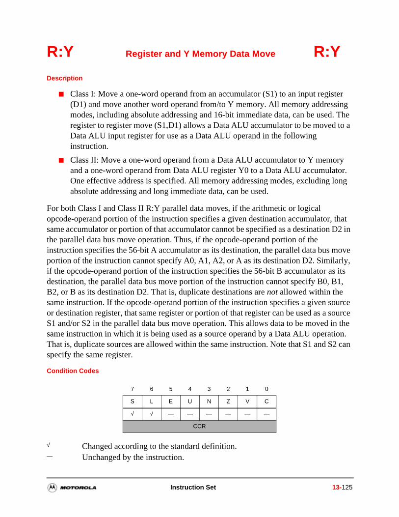
R:Y Register and Y Memory Data Move R:Y
Description
Class I: Move a one-word operand from an accumulator (S1) to an input register (D1) and move another word operand from/to Y memory. All memory addressing modes, including absolute addressing and 16-bit immediate data, can be used. The register to register move (S1,D1) allows a Data ALU accumulator to be moved to a Data ALU input register for use as a Data ALU operand in the following instruction.
Class II: Move a one-word operand from a Data ALU accumulator to Y memory and a one-word operand from Data ALU register Y0 to a Data ALU accumulator. One effective address is specified. All memory addressing modes, excluding long absolute addressing and long immediate data, can be used.
For both Class I and Class II R:Y parallel data moves, if the arithmetic or logical opcode-operand portion of the instruction specifies a given destination accumulator, that same accumulator or portion of that accumulator cannot be specified as a destination D2 in the parallel data bus move operation. Thus, if the opcode-operand portion of the instruction specifies the 56-bit A accumulator as its destination, the parallel data bus move portion of the instruction cannot specify A0, A1, A2, or A as its destination D2. Similarly, if the opcode-operand portion of the instruction specifies the 56-bit B accumulator as its destination, the parallel data bus move portion of the instruction cannot specify B0, B1, B2, or B as its destination D2. That is, duplicate destinations are not allowed within the same instruction. If the opcode-operand portion of the instruction specifies a given source or destination register, that same register or portion of that register can be used as a source S1 and/or S2 in the parallel data bus move operation. This allows data to be moved in the same instruction in which it is being used as a source operand by a Data ALU operation. That is, duplicate sources are allowed within the same instruction. Note that S1 and S2 can specify the same register.
Condition Codes
7 6 5 4 3 2 1 0
S L E U N Z V C
√ √ — — — — — —
CCR
√ Changed according to the standard definition.— Unchanged by the instruction.
Instruction Set 13-125
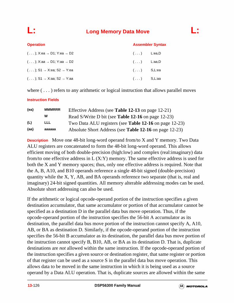
L: Long Memory Data Move L:
where ( . . . ) refers to any arithmetic or logical instruction that allows parallel moves
Instruction Fields
Description Move one 48-bit long-word operand from/to X and Y memory. Two Data ALU registers are concatenated to form the 48-bit long-word operand. This allows efficient moving of both double-precision (high:low) and complex (real:imaginary) data from/to one effective address in L (X:Y) memory. The same effective address is used for both the X and Y memory spaces; thus, only one effective address is required. Note that the A, B, A10, and B10 operands reference a single 48-bit signed (double-precision) quantity while the X, Y, AB, and BA operands reference two separate (that is, real and imaginary) 24-bit signed quantities. All memory alterable addressing modes can be used. Absolute short addressing can also be used.
If the arithmetic or logical opcode-operand portion of the instruction specifies a given destination accumulator, that same accumulator or portion of that accumulator cannot be specified as a destination D in the parallel data bus move operation. Thus, if the opcode-operand portion of the instruction specifies the 56-bit A accumulator as its destination, the parallel data bus move portion of the instruction cannot specify A, A10, AB, or BA as destination D. Similarly, if the opcode-operand portion of the instruction specifies the 56-bit B accumulator as its destination, the parallel data bus move portion of the instruction cannot specify B, B10, AB, or BA as its destination D. That is, duplicate destinations are not allowed within the same instruction. If the opcode-operand portion of the instruction specifies a given source or destination register, that same register or portion of that register can be used as a source S in the parallel data bus move operation. This allows data to be moved in the same instruction in which it is being used as a source operand by a Data ALU operation. That is, duplicate sources are allowed within the same
Operation Assembler Syntax
( . . . ); X:ea → D1; Y:ea → D2 ( . . . ) L:ea,D
( . . . ); X:aa → D1; Y:aa → D2 ( . . . ) L:aa,D
( . . . ); S1 → X:ea; S2 → Y:ea ( . . . ) S,L:ea
( . . . ); S1 → X:aa; S2 → Y:aa ( . . . ) S,L:aa
ea MMMRRR Effective Address (see Table 12-13 on page 12-21)W Read S/Write D bit (see Table 12-16 on page 12-23)
L LLL Two Data ALU registers (see Table 12-16 on page 12-23)aa aaaaaa Absolute Short Address (see Table 12-16 on page 12-23)
13-126 DSP56300 Family Manual
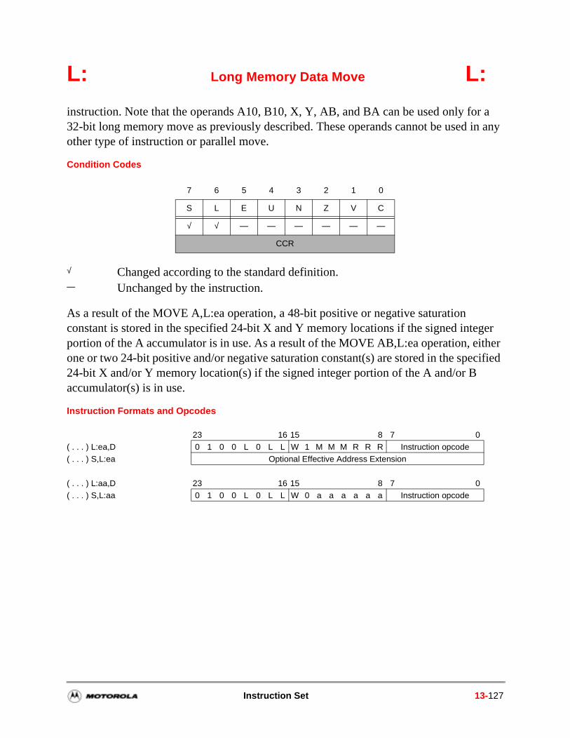
L: Long Memory Data Move L:
instruction. Note that the operands A10, B10, X, Y, AB, and BA can be used only for a 32-bit long memory move as previously described. These operands cannot be used in any other type of instruction or parallel move.
Condition Codes
As a result of the MOVE A,L:ea operation, a 48-bit positive or negative saturation constant is stored in the specified 24-bit X and Y memory locations if the signed integer portion of the A accumulator is in use. As a result of the MOVE AB,L:ea operation, either one or two 24-bit positive and/or negative saturation constant(s) are stored in the specified 24-bit X and/or Y memory location(s) if the signed integer portion of the A and/or B accumulator(s) is in use.
Instruction Formats and Opcodes
7 6 5 4 3 2 1 0
S L E U N Z V C
√ √ — — — — — —
CCR
√ Changed according to the standard definition.— Unchanged by the instruction.
23 16 15 8 7 0( . . . ) L:ea,D 0 1 0 0 L 0 L L W 1 M M M R R R Instruction opcode( . . . ) S,L:ea Optional Effective Address Extension
( . . . ) L:aa,D 23 16 15 8 7 0( . . . ) S,L:aa 0 1 0 0 L 0 L L W 0 a a a a a a Instruction opcode
Instruction Set 13-127
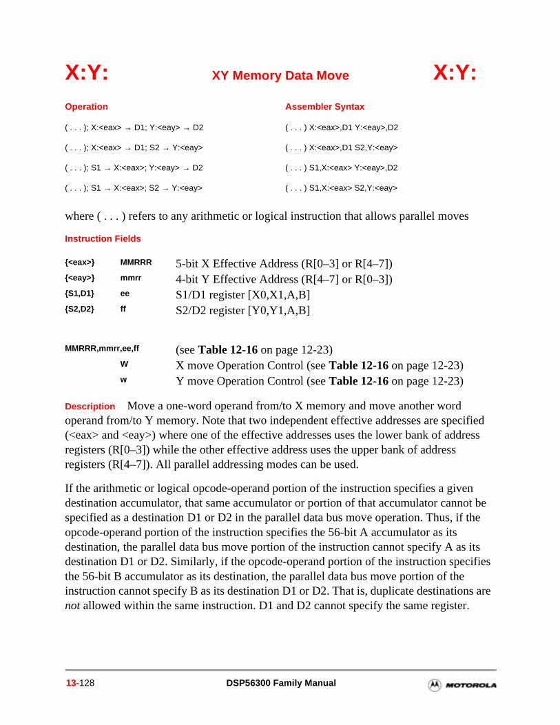
ot be the
its ifies s are .
X:Y: XY Memory Data Move X:Y:
where ( . . . ) refers to any arithmetic or logical instruction that allows parallel moves
Instruction Fields
Description Move a one-word operand from/to X memory and move another word operand from/to Y memory. Note that two independent effective addresses are specified (<eax> and <eay>) where one of the effective addresses uses the lower bank of address registers (R[0–3]) while the other effective address uses the upper bank of address registers (R[4–7]). All parallel addressing modes can be used.
If the arithmetic or logical opcode-operand portion of the instruction specifies a givendestination accumulator, that same accumulator or portion of that accumulator cannspecified as a destination D1 or D2 in the parallel data bus move operation. Thus, ifopcode-operand portion of the instruction specifies the 56-bit A accumulator as its destination, the parallel data bus move portion of the instruction cannot specify A asdestination D1 or D2. Similarly, if the opcode-operand portion of the instruction specthe 56-bit B accumulator as its destination, the parallel data bus move portion of theinstruction cannot specify B as its destination D1 or D2. That is, duplicate destinationnot allowed within the same instruction. D1 and D2 cannot specify the same register
Operation Assembler Syntax
( . . . ); X:<eax> → D1; Y:<eay> → D2 ( . . . ) X:<eax>,D1 Y:<eay>,D2
( . . . ); X:<eax> → D1; S2 → Y:<eay> ( . . . ) X:<eax>,D1 S2,Y:<eay>
( . . . ); S1 → X:<eax>; Y:<eay> → D2 ( . . . ) S1,X:<eax> Y:<eay>,D2
( . . . ); S1 → X:<eax>; S2 → Y:<eay> ( . . . ) S1,X:<eax> S2,Y:<eay>
<eax> MMRRR 5-bit X Effective Address (R[0–3] or R[4–7])<eay> mmrr 4-bit Y Effective Address (R[4–7] or R[0–3])S1,D1 ee S1/D1 register [X0,X1,A,B]S2,D2 ff S2/D2 register [Y0,Y1,A,B]
MMRRR,mmrr,ee,ff (see Table 12-16 on page 12-23)W X move Operation Control (see Table 12-16 on page 12-23)w Y move Operation Control (see Table 12-16 on page 12-23)
13-128 DSP56300 Family Manual
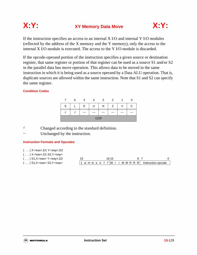
X:Y: XY Memory Data Move X:Y:
If the instruction specifies an access to an internal X I/O and internal Y I/O modules (reflected by the address of the X memory and the Y memory), only the access to the internal X I/O module is executed. The access to the Y I/O module is discarded.
If the opcode-operand portion of the instruction specifies a given source or destination register, that same register or portion of that register can be used as a source S1 and/or S2 in the parallel data bus move operation. This allows data to be moved in the same instruction in which it is being used as a source operand by a Data ALU operation. That is, duplicate sources are allowed within the same instruction. Note that S1 and S2 can specify the same register.
Condition Codes
Instruction Formats and Opcodes
7 6 5 4 3 2 1 0
S L E U N Z V C
√ √ — — — — — —
CCR
√ Changed according to the standard definition.— Unchanged by the instruction.
( . . . ) X:<eax>,D1 Y:<eay>,D2( . . . ) X:<eax>,D1 S2,Y:<eay>( . . . ) S1,X:<eax> Y:<eay>,D2 23 16 15 8 7 0
( . . . ) S1,X:<eax> S2,Y:<eay> 1 w m m e e f f W r r M M R R R Instruction opcode
Instruction Set 13-129
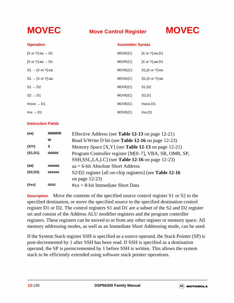
MOVEC Move Control Register MOVEC
Instruction Fields
Description Move the contents of the specified source control register S1 or S2 to the specified destination, or move the specified source to the specified destination control register D1 or D2. The control registers S1 and D1 are a subset of the S2 and D2 register set and consist of the Address ALU modifier registers and the program controller registers. These registers can be moved to or from any other register or memory space. All memory addressing modes, as well as an Immediate Short Addressing mode, can be used.
If the System Stack register SSH is specified as a source operand, the Stack Pointer (SP) is post-decremented by 1 after SSH has been read. If SSH is specified as a destination operand, the SP is preincremented by 1 before SSH is written. This allows the system stack to be efficiently extended using software stack pointer operations.
Operation Assembler Syntax
[X or Y]:ea → D1 MOVE(C) [X or Y]:ea,D1
[X or Y]:aa → D1 MOVE(C) [X or Y]:aa,D1
S1 → [X or Y]:ea MOVE(C) S1,[X or Y]:ea
S1 → [X or Y]:aa MOVE(C) S1,[X or Y]:aa
S1 → D2 MOVE(C) S1,D2
S2 → D1 MOVE(C) S2,D1
#xxxx → D1 MOVE(C) #xxxx,D1
#xx → D1 MOVE(C) #xx,D1
ea MMMRR Effective Address (see Table 12-13 on page 12-21)W Read S/Write D bit (see Table 12-16 on page 12-23)
X/Y S Memory Space [X,Y] (see Table 12-13 on page 12-21)S1,D1 ddddd Program Controller register [M[0–7], VBA, SR, OMR, SP,
SSH,SSL,LA,LC] (see Table 12-16 on page 12-23)aa aaaaaa aa = 6-bit Absolute Short AddressS2,D2 eeeeee S2/D2 register [all on-chip registers] (see Table 12-16
on page 12-23)#xx iiiiiiii #xx = 8-bit Immediate Short Data
13-130 DSP56300 Family Manual
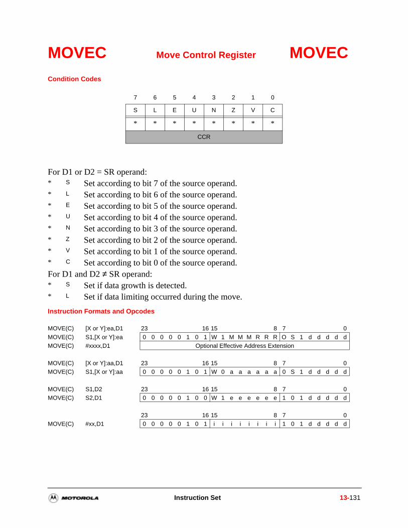
MOVEC Move Control Register MOVECCondition Codes
Instruction Formats and Opcodes
7 6 5 4 3 2 1 0
S L E U N Z V C
* * * * * * * *
CCR
For D1 or D2 = SR operand:* S Set according to bit 7 of the source operand.* L Set according to bit 6 of the source operand.* E Set according to bit 5 of the source operand.* U Set according to bit 4 of the source operand.* N Set according to bit 3 of the source operand.* Z Set according to bit 2 of the source operand.* V Set according to bit 1 of the source operand.* C Set according to bit 0 of the source operand. For D1 and D2 ≠ SR operand:* S Set if data growth is detected. * L Set if data limiting occurred during the move.
MOVE(C) [X or Y]:ea,D1 23 16 15 8 7 0
MOVE(C) S1,[X or Y]:ea 0 0 0 0 0 1 0 1 W 1 M M M R R R O S 1 d d d d dMOVE(C) #xxxx,D1 Optional Effective Address Extension
MOVE(C) [X or Y]:aa,D1 23 16 15 8 7 0MOVE(C) S1,[X or Y]:aa 0 0 0 0 0 1 0 1 W 0 a a a a a a 0 S 1 d d d d d
MOVE(C) S1,D2 23 16 15 8 7 0MOVE(C) S2,D1 0 0 0 0 0 1 0 0 W 1 e e e e e e 1 0 1 d d d d d
23 16 15 8 7 0MOVE(C) #xx,D1 0 0 0 0 0 1 0 1 i i i i i i i i 1 0 1 d d d d d
Instruction Set 13-131
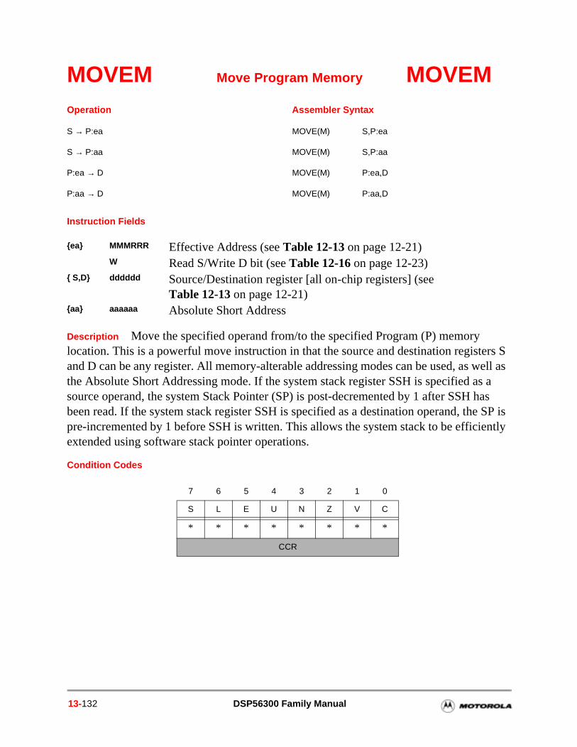
MOVEM Move Program Memory MOVEM
Instruction Fields
Description Move the specified operand from/to the specified Program (P) memory location. This is a powerful move instruction in that the source and destination registers S and D can be any register. All memory-alterable addressing modes can be used, as well as the Absolute Short Addressing mode. If the system stack register SSH is specified as a source operand, the system Stack Pointer (SP) is post-decremented by 1 after SSH has been read. If the system stack register SSH is specified as a destination operand, the SP is pre-incremented by 1 before SSH is written. This allows the system stack to be efficiently extended using software stack pointer operations.
Condition Codes
Operation Assembler Syntax
S → P:ea MOVE(M) S,P:ea
S → P:aa MOVE(M) S,P:aa
P:ea → D MOVE(M) P:ea,D
P:aa → D MOVE(M) P:aa,D
ea MMMRRR Effective Address (see Table 12-13 on page 12-21)W Read S/Write D bit (see Table 12-16 on page 12-23)
S,D dddddd Source/Destination register [all on-chip registers] (see Table 12-13 on page 12-21)
aa aaaaaa Absolute Short Address
7 6 5 4 3 2 1 0
S L E U N Z V C
* * * * * * * *
CCR
13-132 DSP56300 Family Manual
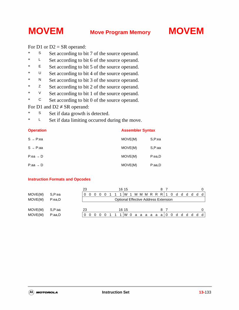
MOVEM Move Program Memory MOVEM
Instruction Formats and Opcodes
For D1 or D2 = SR operand: * S Set according to bit 7 of the source operand.* L Set according to bit 6 of the source operand.* E Set according to bit 5 of the source operand.* U Set according to bit 4 of the source operand.* N Set according to bit 3 of the source operand.* Z Set according to bit 2 of the source operand.* V Set according to bit 1 of the source operand.* C Set according to bit 0 of the source operand. For D1 and D2 ≠ SR operand:* S Set if data growth is detected. * L Set if data limiting occurred during the move.
Operation Assembler Syntax
S → P:ea MOVE(M) S,P:ea
S → P:aa MOVE(M) S,P:aa
P:ea → D MOVE(M) P:ea,D
P:aa → D MOVE(M) P:aa,D
23 16 15 8 7 0
MOVE(M) S,P:ea 0 0 0 0 0 1 1 1 W 1 M M M R R R 1 0 d d d d d dMOVE(M) P:ea,D Optional Effective Address Extension
MOVE(M) S,P:aa 23 16 15 8 7 0MOVE(M) P:aa,D 0 0 0 0 0 1 1 1 W 0 a a a a a a 0 0 d d d d d d
Instruction Set 13-133
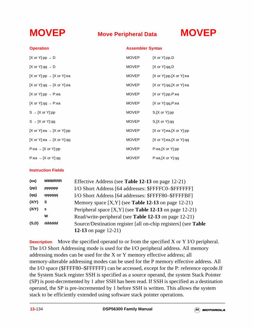
de.If Pointer tination em
MOVEP Move Peripheral Data MOVEP
Instruction Fields
Description Move the specified operand to or from the specified X or Y I/O peripheral. The I/O Short Addressing mode is used for the I/O peripheral address. All memory addressing modes can be used for the X or Y memory effective address; all memory-alterable addressing modes can be used for the P memory effective address. All the I/O space ($FFFF80–$FFFFFF) can be accessed, except for the P: reference opcothe System Stack register SSH is specified as a source operand, the system Stack (SP) is post-decremented by 1 after SSH has been read. If SSH is specified as a desoperand, the SP is pre-incremented by 1 before SSH is written. This allows the syststack to be efficiently extended using software stack pointer operations.
Operation Assembler Syntax
[X or Y]:pp → D MOVEP [X or Y]:pp,D
[X or Y]:qq → D MOVEP [X or Y]:qq,D
[X or Y]:pp → [X or Y]:ea MOVEP [X or Y]:pp,[X or Y]:ea
[X or Y]:qq → [X or Y]:ea MOVEP [X or Y]:qq,[X or Y]:ea
[X or Y]:pp → P:ea MOVEP [X or Y]:pp,P:ea
[X or Y]:qq → P:ea MOVEP [X or Y]:qq,P:ea
S → [X or Y]:pp MOVEP S,[X or Y]:pp
S → [X or Y]:qq MOVEP S,[X or Y]:qq
[X or Y]:ea → [X or Y]:pp MOVEP [X or Y]:ea,[X or Y]:pp
[X or Y]:ea → [X or Y]:qq MOVEP [X or Y]:ea,[X or Y]:qq
P:ea → [X or Y]:pp MOVEP P:ea,[X or Y]:pp
P:ea → [X or Y]:qq MOVEP P:ea,[X or Y]:qq
ea MMMRRR Effective Address (see Table 12-13 on page 12-21)pp pppppp I/O Short Address [64 addresses: $FFFFC0–$FFFFFF]qq qqqqqq I/O Short Address [64 addresses: $FFFF80–$FFFFBF]X/Y S Memory space [X,Y] (see Table 12-13 on page 12-21)X/Y s Peripheral space [X,Y] (see Table 12-13 on page 12-21)
W Read/write-peripheral (see Table 12-13 on page 12-21)S,D dddddd Source/Destination register [all on-chip registers] (see Table
12-13 on page 12-21)
13-134 DSP56300 Family Manual
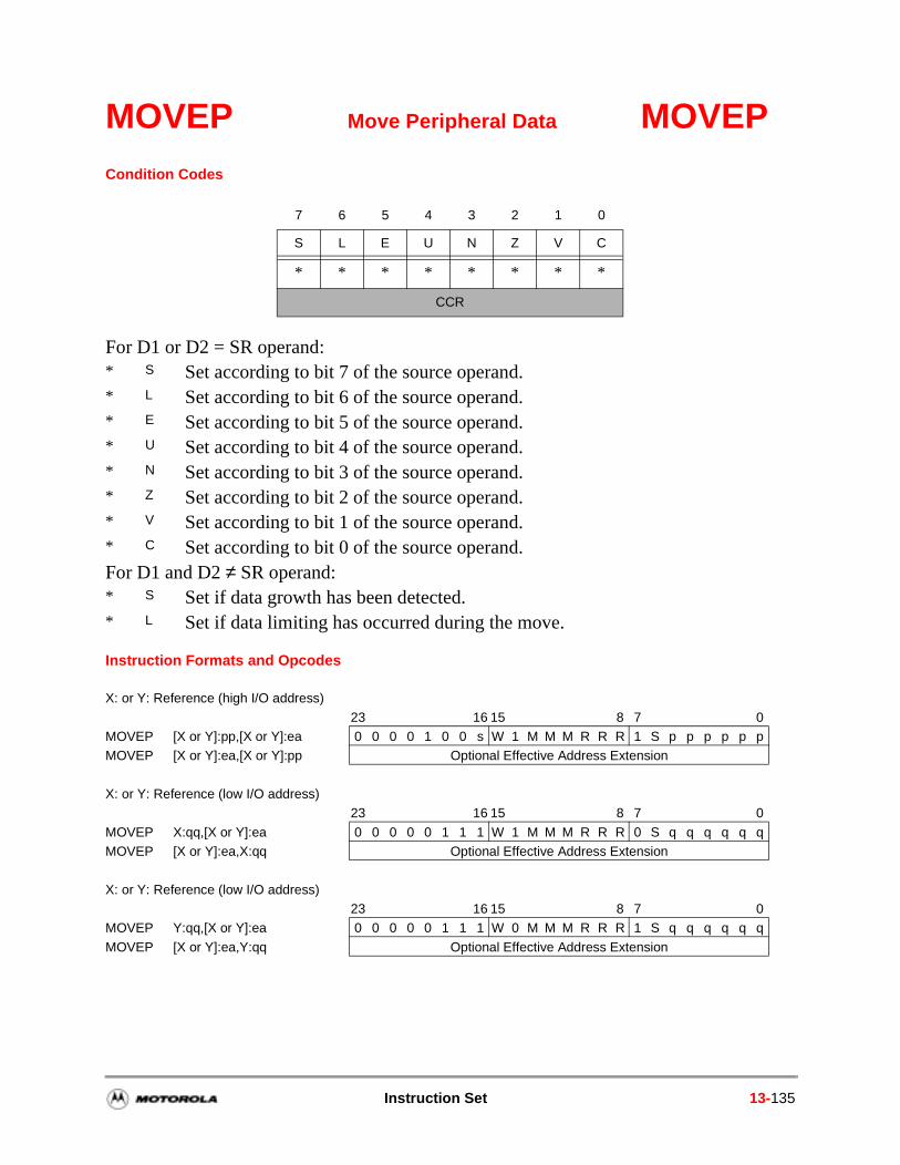
MOVEP Move Peripheral Data MOVEPCondition Codes
Instruction Formats and Opcodes
7 6 5 4 3 2 1 0
S L E U N Z V C
* * * * * * * *
CCR
For D1 or D2 = SR operand: * S Set according to bit 7 of the source operand.* L Set according to bit 6 of the source operand.* E Set according to bit 5 of the source operand.* U Set according to bit 4 of the source operand.* N Set according to bit 3 of the source operand.* Z Set according to bit 2 of the source operand.* V Set according to bit 1 of the source operand.* C Set according to bit 0 of the source operand. For D1 and D2 ≠ SR operand:* S Set if data growth has been detected. * L Set if data limiting has occurred during the move.
X: or Y: Reference (high I/O address)
23 16 15 8 7 0MOVEP [X or Y]:pp,[X or Y]:ea 0 0 0 0 1 0 0 s W 1 M M M R R R 1 S p p p p p pMOVEP [X or Y]:ea,[X or Y]:pp Optional Effective Address Extension
X: or Y: Reference (low I/O address)23 16 15 8 7 0
MOVEP X:qq,[X or Y]:ea 0 0 0 0 0 1 1 1 W 1 M M M R R R 0 S q q q q q qMOVEP [X or Y]:ea,X:qq Optional Effective Address Extension
X: or Y: Reference (low I/O address)23 16 15 8 7 0
MOVEP Y:qq,[X or Y]:ea 0 0 0 0 0 1 1 1 W 0 M M M R R R 1 S q q q q q q
MOVEP [X or Y]:ea,Y:qq Optional Effective Address Extension
Instruction Set 13-135
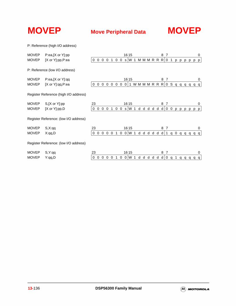
MOVEP Move Peripheral Data MOVEPP: Reference (high I/O address)
MOVEP P:ea,[X or Y]:pp 16 15 8 7 0MOVEP [X or Y]:pp,P:ea 0 0 0 0 1 0 0 s W 1 M M M R R R 0 1 p p p p p p
P: Reference (low I/O address)
MOVEP P:ea,[X or Y]:qq 16 15 8 7 0MOVEP [X or Y]:qq,P:ea 0 0 0 0 0 0 0 0 1 W M M M R R R 0 S q q q q q q
Register Reference (high I/O address)
MOVEP S,[X or Y]:pp 23 16 15 8 7 0MOVEP [X or Y]:pp,D 0 0 0 0 1 0 0 s W 1 d d d d d d 0 0 p p p p p p
Register Reference: (low I/O address)
MOVEP S,X:qq 23 16 15 8 7 0MOVEP X:qq,D 0 0 0 0 0 1 0 0 W 1 d d d d d d 1 q 0 q q q q q
Register Reference: (low I/O address)
MOVEP S,Y:qq 23 16 15 8 7 0MOVEP Y:qq,D 0 0 0 0 0 1 0 0 W 1 d d d d d d 0 q 1 q q q q q
13-136 DSP56300 Family Manual
n is s “+”. ons cision
MPY Signed Multiply MPY
Instruction Fields 1
Instruction Fields 2
Description Multiply the two signed 24-bit source operands S1 and S2 and store the resulting product in the specified 56-bit destination accumulator D. Or, multiply the signed 24-bit source operand S by the positive 24-bit immediate operand 2-n and store the resulting product in the specified 56-bit destination accumulator D. The “–” sign optioused to negate the specified product prior to accumulation. The default sign option iWhen the processor is in the Double-Precision Multiply mode, the following instructido not execute in the normal way and should be used only as part of the double-premultiply algorithm:
MPY Y0,X0,A MPY Y0,X0,B
Operation Assembler Syntax
±S1 ∗ S2 → D (parallel move) MPY (±)S1,S2,D (parallel move)
±S1 ∗ S2 → D (parallel move) MPY (±)S2,S1,D (parallel move)
±(S1 ∗ 2-n) → D (no parallel move) MPY (±)S,#n,D (no parallel move)
S1,S2 QQQ Source registers S1,S2 [X0*X0, Y0*Y0, X1*X0, Y1*Y0, X0*Y1, Y0*X0, X1*Y0, Y1*X1] (see Table 12-16 on page 12-23)
D d Destination accumulator [A,B] (see Table 12-13 on page 12-21)± k Sign [+,–] (see Table 12-16 on page 12-23)
S QQ Source register [Y1,X0,Y0,X1] (see Table 12-16 on page 12-23)D d Destination accumulator [A,B] (see Table 12-13 on page 12-21)± k Sign [+,–] (see Table 12-16 on page 12-23)#n sssss Immediate operand (see Table 12-16 on page 12-23)
Instruction Set 13-137
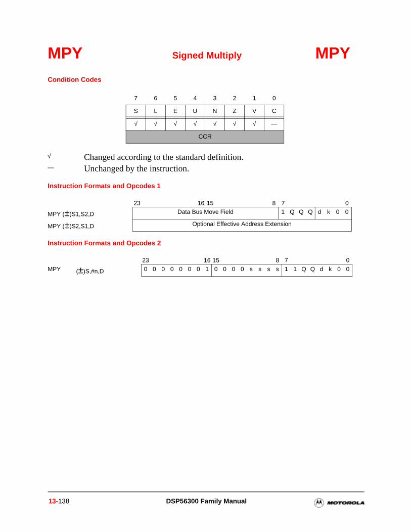
MPY Signed Multiply MPYCondition Codes
Instruction Formats and Opcodes 1
Instruction Formats and Opcodes 2
7 6 5 4 3 2 1 0
S L E U N Z V C
√ √ √ √ √ √ √ —
CCR
√ Changed according to the standard definition.— Unchanged by the instruction.
23 16 15 8 7 0
MPY (±)S1,S2,D Data Bus Move Field 1 Q Q Q d k 0 0
MPY (±)S2,S1,D Optional Effective Address Extension
23 16 15 8 7 0
MPY (±)S,#n,D 0 0 0 0 0 0 0 1 0 0 0 0 s s s s 1 1 Q Q d k 0 0
13-138 DSP56300 Family Manual
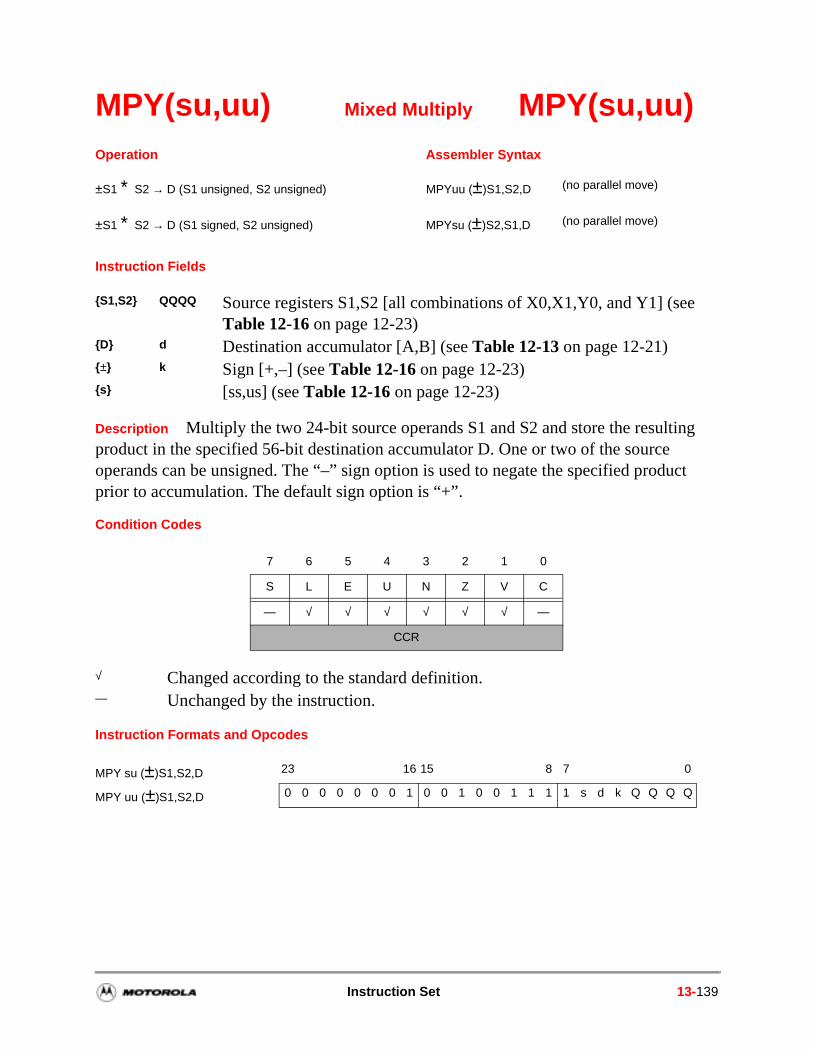
ct
MPY(su,uu) Mixed Multiply MPY(su,uu)
Instruction Fields
Description Multiply the two 24-bit source operands S1 and S2 and store the resulting product in the specified 56-bit destination accumulator D. One or two of the source operands can be unsigned. The “–” sign option is used to negate the specified produprior to accumulation. The default sign option is “+”.
Condition Codes
Instruction Formats and Opcodes
Operation Assembler Syntax
±S1 ∗ S2 → D (S1 unsigned, S2 unsigned) MPYuu (±)S1,S2,D (no parallel move)
±S1 ∗ S2 → D (S1 signed, S2 unsigned) MPYsu (±)S2,S1,D (no parallel move)
S1,S2 QQQQ Source registers S1,S2 [all combinations of X0,X1,Y0, and Y1] (seeTable 12-16 on page 12-23)
D d Destination accumulator [A,B] (see Table 12-13 on page 12-21)± k Sign [+,–] (see Table 12-16 on page 12-23)s [ss,us] (see Table 12-16 on page 12-23)
7 6 5 4 3 2 1 0
S L E U N Z V C
— √ √ √ √ √ √ —
CCR
√ Changed according to the standard definition. — Unchanged by the instruction.
MPY su (±)S1,S2,D 23 16 15 8 7 0
MPY uu (±)S1,S2,D 0 0 0 0 0 0 0 1 0 0 1 0 0 1 1 1 1 s d k Q Q Q Q
Instruction Set 13-139
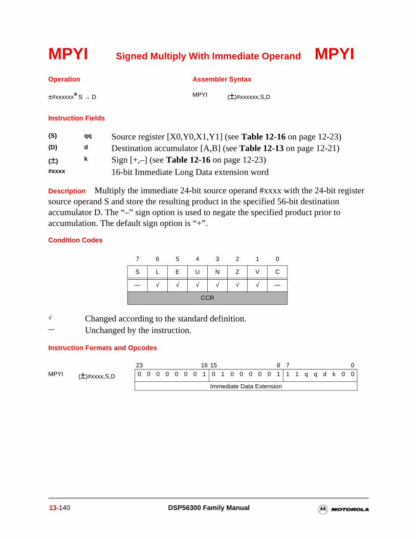
MPYI Signed Multiply With Immediate Operand MPYI
Instruction Fields
Description Multiply the immediate 24-bit source operand #xxxx with the 24-bit register source operand S and store the resulting product in the specified 56-bit destination accumulator D. The “–” sign option is used to negate the specified product prior to accumulation. The default sign option is “+”.
Condition Codes
Instruction Formats and Opcodes
Operation Assembler Syntax
±#xxxxxx∗S → D MPYI (±)#xxxxxx,S,D
S qq Source register [X0,Y0,X1,Y1] (see Table 12-16 on page 12-23)D d Destination accumulator [A,B] (see Table 12-13 on page 12-21)± k Sign [+,–] (see Table 12-16 on page 12-23)#xxxx 16-bit Immediate Long Data extension word
7 6 5 4 3 2 1 0
S L E U N Z V C
— √ √ √ √ √ √ —
CCR
√ Changed according to the standard definition. — Unchanged by the instruction.
23 16 15 8 7 0MPYI (±)#xxxx,S,D 0 0 0 0 0 0 0 1 0 1 0 0 0 0 0 1 1 1 q q d k 0 0
Immediate Data Extension
13-140 DSP56300 Family Manual
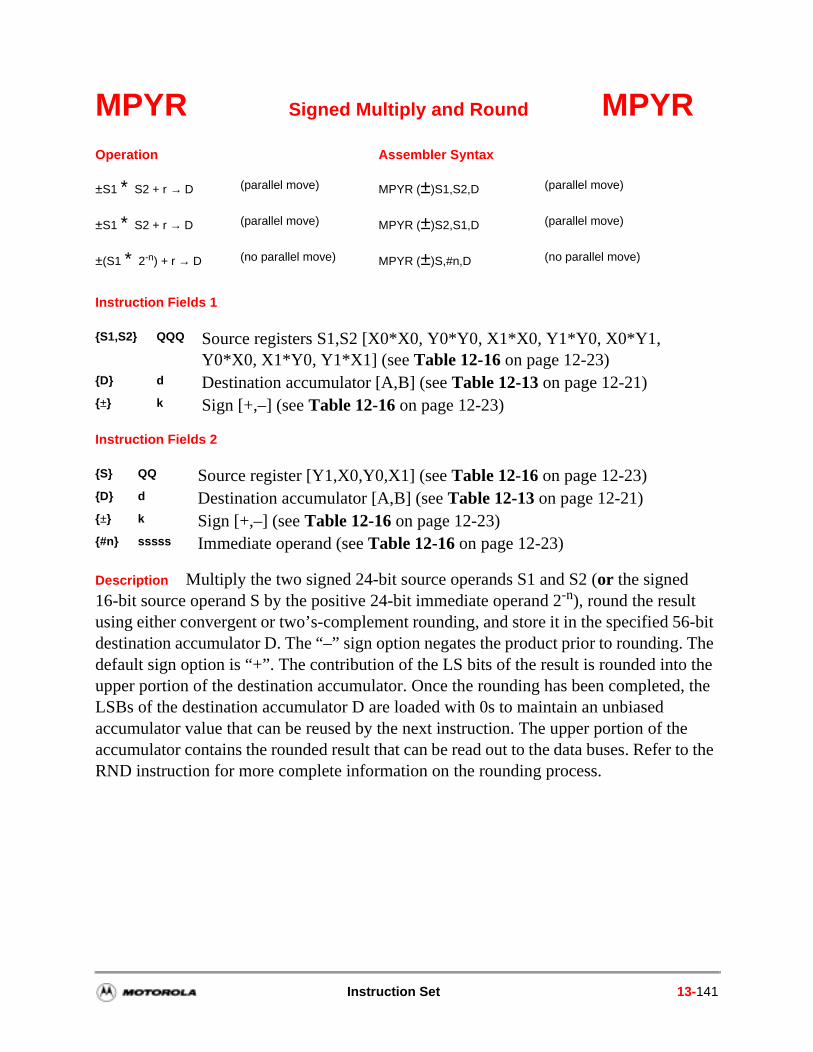
6-bit . The the d, the
he r to the
MPYR Signed Multiply and Round MPYR
Instruction Fields 1
Instruction Fields 2
Description Multiply the two signed 24-bit source operands S1 and S2 (or the signed 16-bit source operand S by the positive 24-bit immediate operand 2-n), round the result using either convergent or two’s-complement rounding, and store it in the specified 5destination accumulator D. The “–” sign option negates the product prior to roundingdefault sign option is “+”. The contribution of the LS bits of the result is rounded intoupper portion of the destination accumulator. Once the rounding has been completeLSBs of the destination accumulator D are loaded with 0s to maintain an unbiased accumulator value that can be reused by the next instruction. The upper portion of taccumulator contains the rounded result that can be read out to the data buses. RefeRND instruction for more complete information on the rounding process.
Operation Assembler Syntax
±S1 ∗ S2 + r → D (parallel move) MPYR (±)S1,S2,D (parallel move)
±S1 ∗ S2 + r → D (parallel move) MPYR (±)S2,S1,D (parallel move)
±(S1 ∗ 2-n) + r → D (no parallel move) MPYR (±)S,#n,D (no parallel move)
S1,S2 QQQ Source registers S1,S2 [X0*X0, Y0*Y0, X1*X0, Y1*Y0, X0*Y1, Y0*X0, X1*Y0, Y1*X1] (see Table 12-16 on page 12-23)
D d Destination accumulator [A,B] (see Table 12-13 on page 12-21)± k Sign [+,–] (see Table 12-16 on page 12-23)
S QQ Source register [Y1,X0,Y0,X1] (see Table 12-16 on page 12-23) D d Destination accumulator [A,B] (see Table 12-13 on page 12-21)± k Sign [+,–] (see Table 12-16 on page 12-23)#n sssss Immediate operand (see Table 12-16 on page 12-23)
Instruction Set 13-141
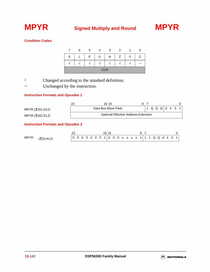
MPYR Signed Multiply and Round MPYRCondition Codes
Instruction Formats and Opcodes 1
Instruction Formats and Opcodes 2
7 6 5 4 3 2 1 0
S L E U N Z V C
√ √ √ √ √ √ √ —
CCR
√ Changed according to the standard definition.— Unchanged by the instruction.
23 16 15 8 7 0
MPYR (±)S1,S2,D Data Bus Move Field 1 Q Q Q d k 0 1
MPYR (±)S2,S1,D Optional Effective Address Extension
23 16 15 8 7 0
MPYR (±)S,#n,D 0 0 0 0 0 0 0 1 0 0 0 s s s s s 1 1 Q Q d k 0 1
13-142 DSP56300 Family Manual
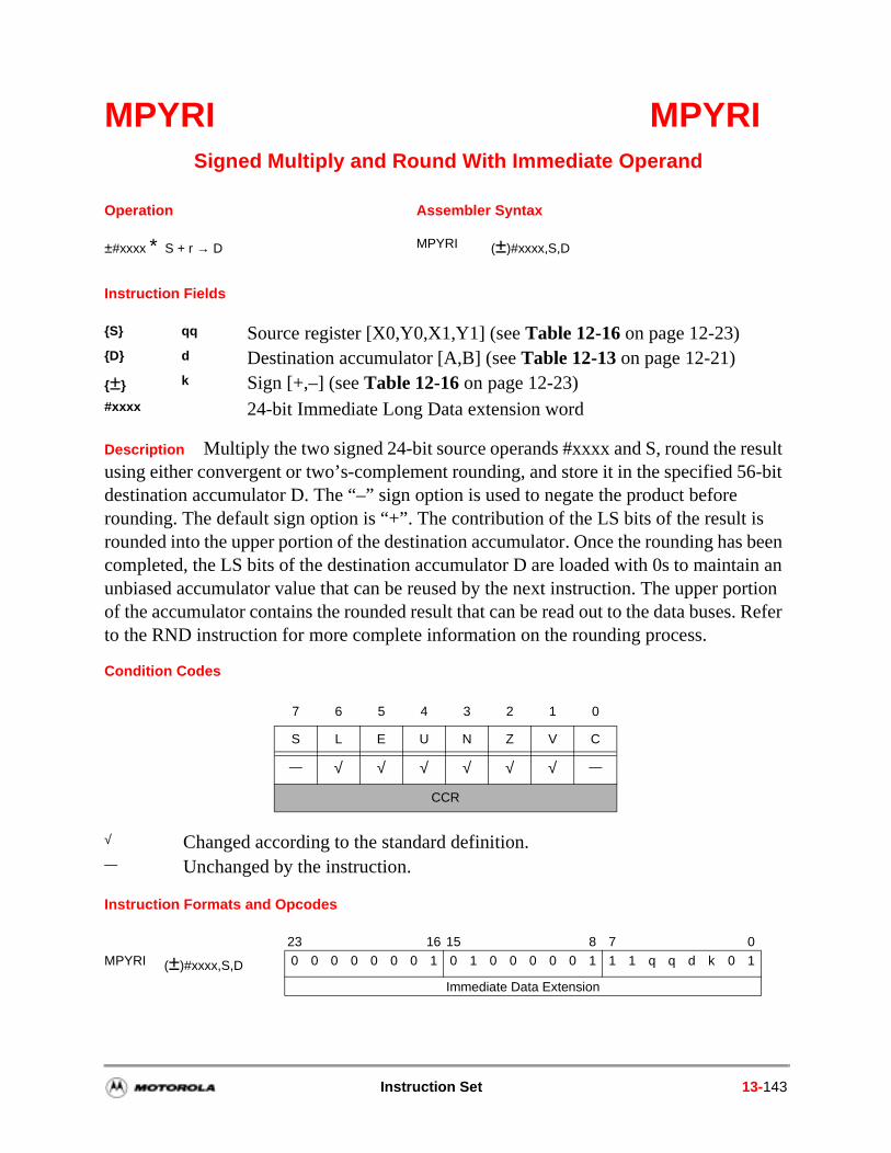
6-bit
s s been in an ortion s. Refer
MPYRI MPYRI Signed Multiply and Round With Immediate Operand
Instruction Fields
Description Multiply the two signed 24-bit source operands #xxxx and S, round the result using either convergent or two’s-complement rounding, and store it in the specified 5destination accumulator D. The “–” sign option is used to negate the product before rounding. The default sign option is “+”. The contribution of the LS bits of the result irounded into the upper portion of the destination accumulator. Once the rounding hacompleted, the LS bits of the destination accumulator D are loaded with 0s to maintaunbiased accumulator value that can be reused by the next instruction. The upper pof the accumulator contains the rounded result that can be read out to the data buseto the RND instruction for more complete information on the rounding process.
Condition Codes
Instruction Formats and Opcodes
Operation Assembler Syntax
±#xxxx ∗ S + r → D MPYRI (±)#xxxx,S,D
S qq Source register [X0,Y0,X1,Y1] (see Table 12-16 on page 12-23)D d Destination accumulator [A,B] (see Table 12-13 on page 12-21)± k Sign [+,–] (see Table 12-16 on page 12-23)#xxxx 24-bit Immediate Long Data extension word
7 6 5 4 3 2 1 0
S L E U N Z V C
— √ √ √ √ √ √ —
CCR
√ Changed according to the standard definition. — Unchanged by the instruction.
23 16 15 8 7 0MPYRI (±)#xxxx,S,D 0 0 0 0 0 0 0 1 0 1 0 0 0 0 0 1 1 1 q q d k 0 1
Immediate Data Extension
Instruction Set 13-143
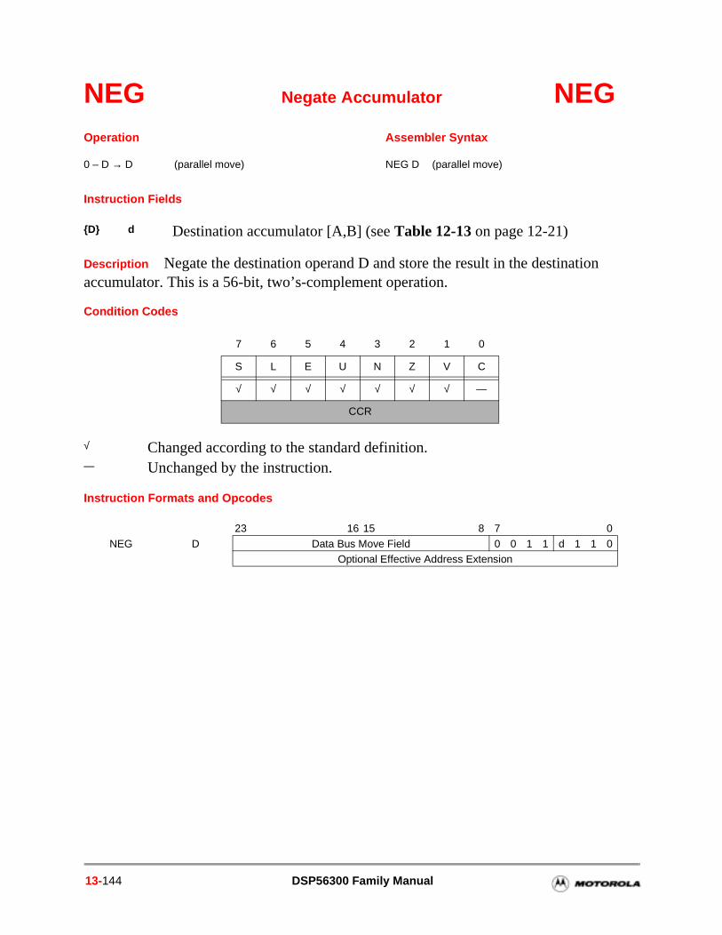
NEG Negate Accumulator NEG
Instruction Fields
Description Negate the destination operand D and store the result in the destination accumulator. This is a 56-bit, two’s-complement operation.
Condition Codes
Instruction Formats and Opcodes
Operation Assembler Syntax
0 – D → D (parallel move) NEG D (parallel move)
D d Destination accumulator [A,B] (see Table 12-13 on page 12-21)
7 6 5 4 3 2 1 0
S L E U N Z V C
√ √ √ √ √ √ √ —
CCR
√ Changed according to the standard definition. — Unchanged by the instruction.
23 16 15 8 7 0
NEG D Data Bus Move Field 0 0 1 1 d 1 1 0Optional Effective Address Extension
13-144 DSP56300 Family Manual
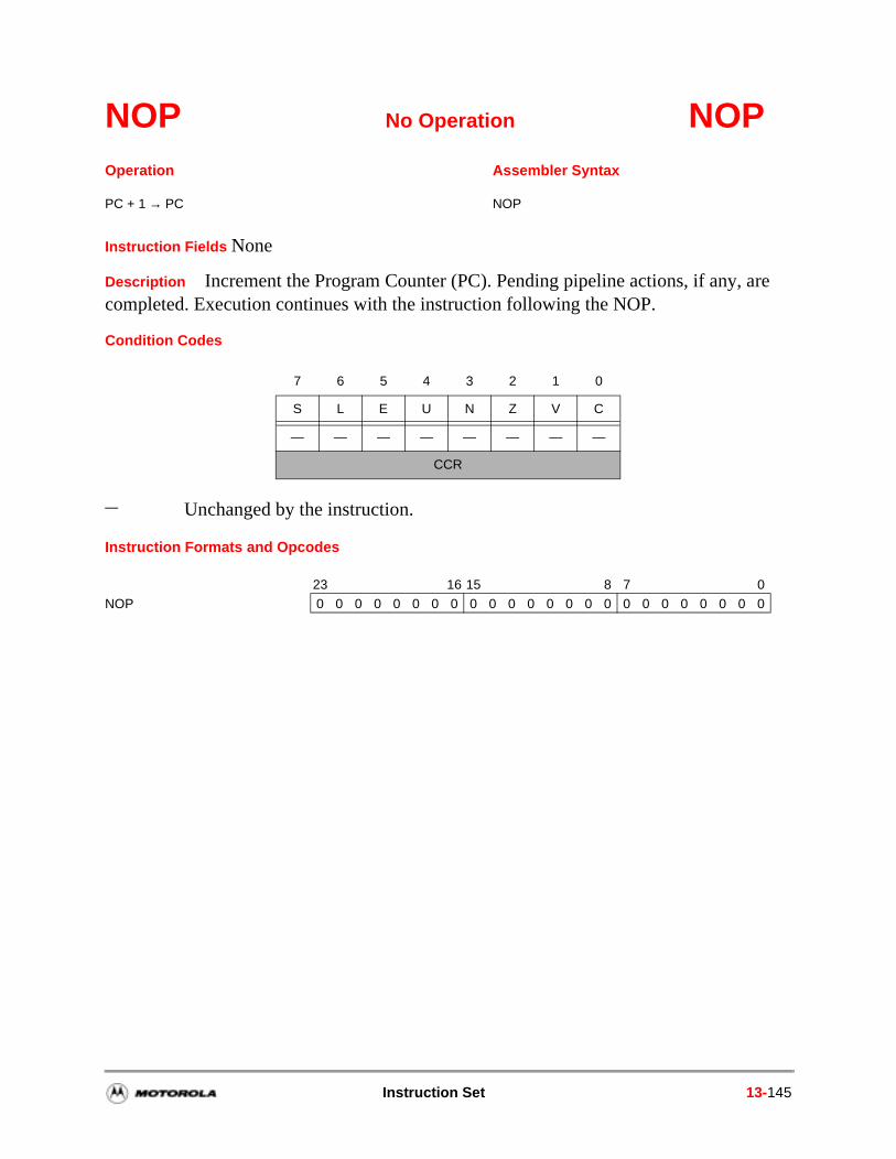
NOP No Operation NOP
Instruction Fields None
Description Increment the Program Counter (PC). Pending pipeline actions, if any, are completed. Execution continues with the instruction following the NOP.
Condition Codes
Instruction Formats and Opcodes
Operation Assembler Syntax
PC + 1 → PC NOP
7 6 5 4 3 2 1 0
S L E U N Z V C
— — — — — — — —
CCR
— Unchanged by the instruction.
23 16 15 8 7 0
NOP 0 0 0 0 0 0 0 0 0 0 0 0 0 0 0 0 0 0 0 0 0 0 0 0
Instruction Set 13-145
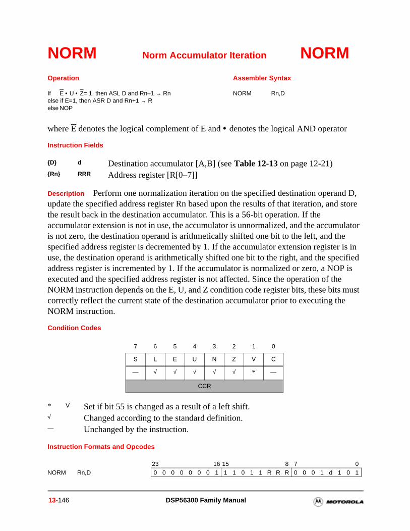
NORM Norm Accumulator Iteration NORM
where E denotes the logical complement of E and • denotes the logical AND operator
Instruction Fields
Description Perform one normalization iteration on the specified destination operand D, update the specified address register Rn based upon the results of that iteration, and store the result back in the destination accumulator. This is a 56-bit operation. If the accumulator extension is not in use, the accumulator is unnormalized, and the accumulator is not zero, the destination operand is arithmetically shifted one bit to the left, and the specified address register is decremented by 1. If the accumulator extension register is in use, the destination operand is arithmetically shifted one bit to the right, and the specified address register is incremented by 1. If the accumulator is normalized or zero, a NOP is executed and the specified address register is not affected. Since the operation of the NORM instruction depends on the E, U, and Z condition code register bits, these bits must correctly reflect the current state of the destination accumulator prior to executing the NORM instruction.
Condition Codes
Instruction Formats and Opcodes
Operation Assembler Syntax
If E • U • Z= 1, then ASL D and Rn–1 → Rnelse if E=1, then ASR D and Rn+1 → Relse NOP
NORM Rn,D
D d Destination accumulator [A,B] (see Table 12-13 on page 12-21)Rn RRR Address register [R[0–7]]
7 6 5 4 3 2 1 0
S L E U N Z V C
— √ √ √ √ √ * —
CCR
* V Set if bit 55 is changed as a result of a left shift.√ Changed according to the standard definition.— Unchanged by the instruction.
23 16 15 8 7 0NORM Rn,D 0 0 0 0 0 0 0 1 1 1 0 1 1 R R R 0 0 0 1 d 1 0 1
13-146 DSP56300 Family Manual
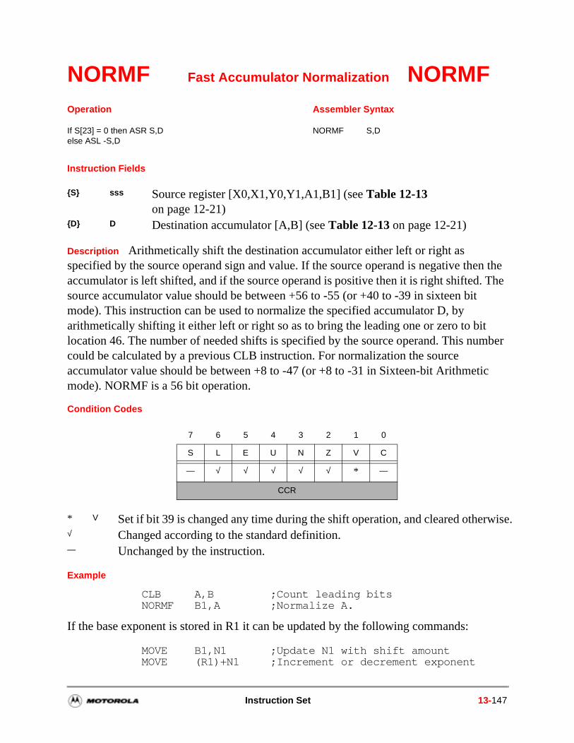
NORMF Fast Accumulator Normalization NORMF
Instruction Fields
Description Arithmetically shift the destination accumulator either left or right as specified by the source operand sign and value. If the source operand is negative then the accumulator is left shifted, and if the source operand is positive then it is right shifted. The source accumulator value should be between +56 to -55 (or +40 to -39 in sixteen bit mode). This instruction can be used to normalize the specified accumulator D, by arithmetically shifting it either left or right so as to bring the leading one or zero to bit location 46. The number of needed shifts is specified by the source operand. This number could be calculated by a previous CLB instruction. For normalization the source accumulator value should be between +8 to -47 (or +8 to -31 in Sixteen-bit Arithmetic mode). NORMF is a 56 bit operation.
Condition Codes
Example
CLB A,B ;Count leading bitsNORMF B1,A ;Normalize A.
If the base exponent is stored in R1 it can be updated by the following commands:
MOVE B1,N1 ;Update N1 with shift amountMOVE (R1)+N1 ;Increment or decrement exponent
Operation Assembler Syntax
If S[23] = 0 then ASR S,Delse ASL -S,D
NORMF S,D
S sss Source register [X0,X1,Y0,Y1,A1,B1] (see Table 12-13 on page 12-21)
D D Destination accumulator [A,B] (see Table 12-13 on page 12-21)
7 6 5 4 3 2 1 0
S L E U N Z V C
— √ √ √ √ √ * —
CCR
* V Set if bit 39 is changed any time during the shift operation, and cleared otherwise. √ Changed according to the standard definition. — Unchanged by the instruction.
Instruction Set 13-147
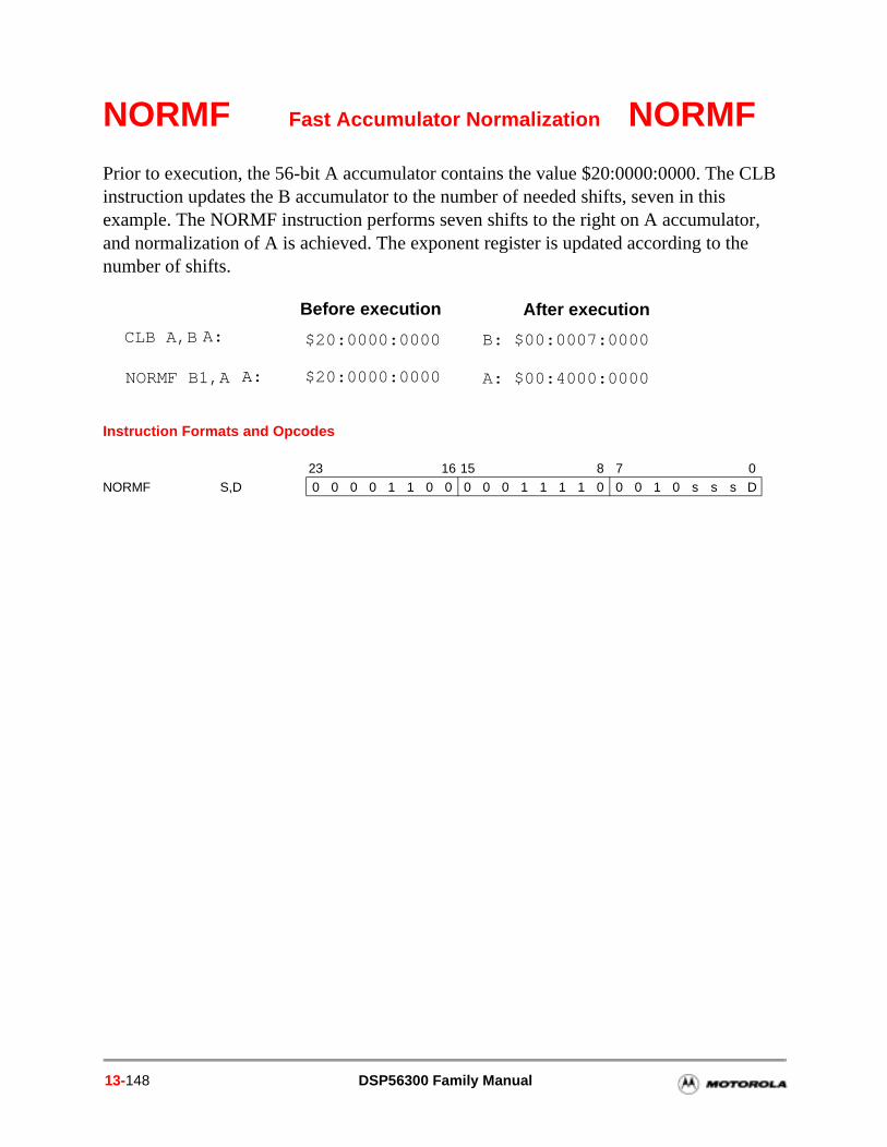
NORMF Fast Accumulator Normalization NORMF
Prior to execution, the 56-bit A accumulator contains the value $20:0000:0000. The CLB instruction updates the B accumulator to the number of needed shifts, seven in this example. The NORMF instruction performs seven shifts to the right on A accumulator, and normalization of A is achieved. The exponent register is updated according to the number of shifts.
Instruction Formats and Opcodes
23 16 15 8 7 0NORMF S,D 0 0 0 0 1 1 0 0 0 0 0 1 1 1 1 0 0 0 1 0 s s s D
$20:0000:0000
B: $00:0007:0000
A:
Before execution
$20:0000:0000
After execution
A: $00:4000:0000
A:CLB A,B
NORMF B1,A
13-148 DSP56300 Family Manual
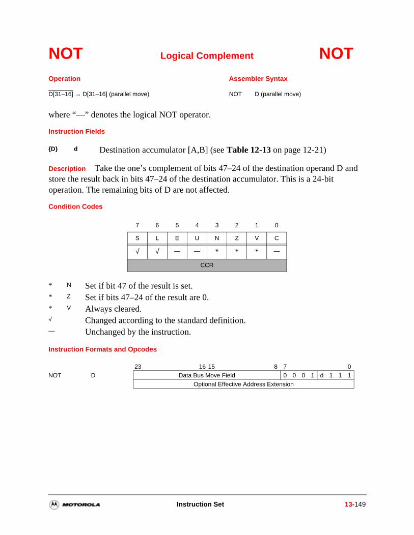
nd
NOT Logical Complement NOT
where “—” denotes the logical NOT operator.
Instruction Fields
Description Take the one’s complement of bits 47–24 of the destination operand D astore the result back in bits 47–24 of the destination accumulator. This is a 24-bit operation. The remaining bits of D are not affected.
Condition Codes
Instruction Formats and Opcodes
Operation Assembler Syntax
D[31–16] → D[31–16] (parallel move) NOT D (parallel move)
D d Destination accumulator [A,B] (see Table 12-13 on page 12-21)
7 6 5 4 3 2 1 0
S L E U N Z V C
√ √ — — * * * —
CCR
* N Set if bit 47 of the result is set.* Z Set if bits 47–24 of the result are 0.* V Always cleared. √ Changed according to the standard definition.— Unchanged by the instruction.
23 16 15 8 7 0NOT D Data Bus Move Field 0 0 0 1 d 1 1 1
Optional Effective Address Extension
Instruction Set 13-149
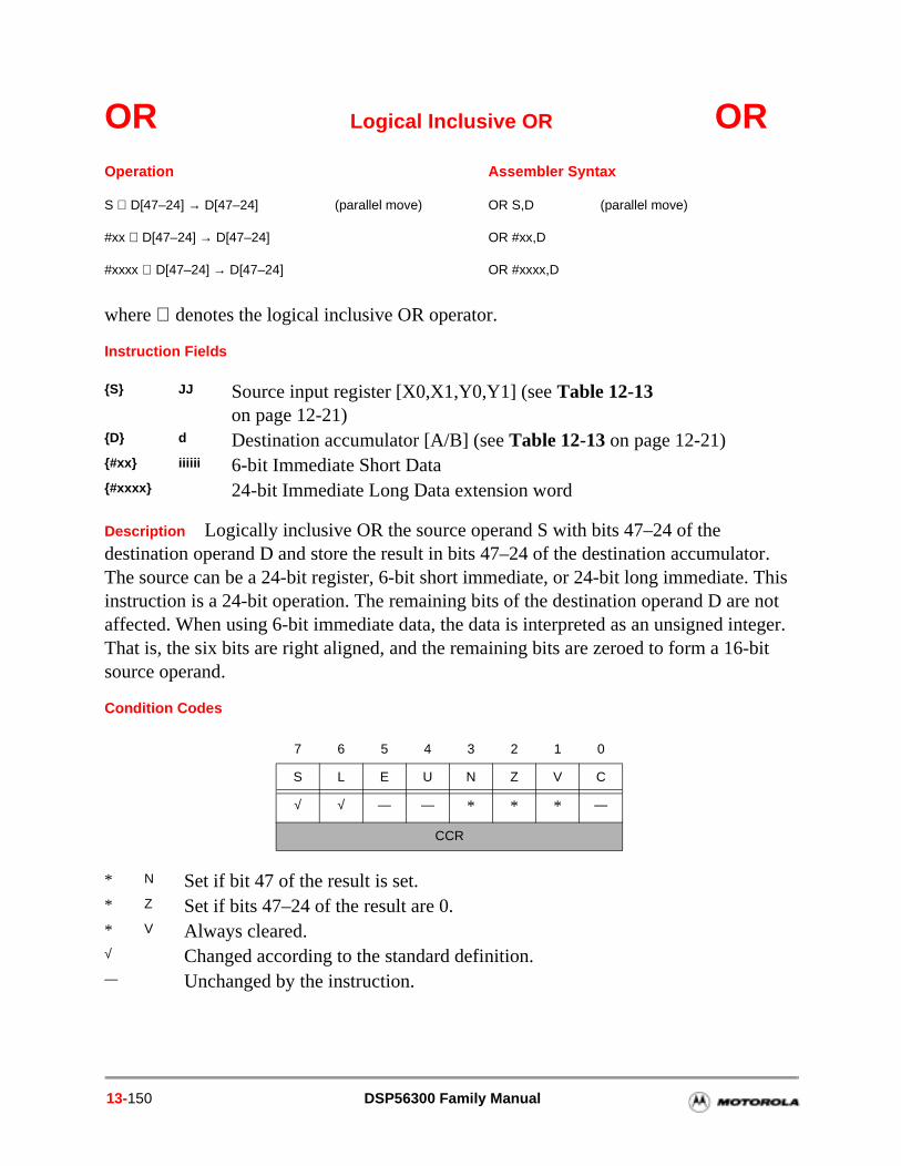
tor. This not teger.
-bit
OR Logical Inclusive OR OR
where ⊕ denotes the logical inclusive OR operator.
Instruction Fields
Description Logically inclusive OR the source operand S with bits 47–24 of the destination operand D and store the result in bits 47–24 of the destination accumulaThe source can be a 24-bit register, 6-bit short immediate, or 24-bit long immediate.instruction is a 24-bit operation. The remaining bits of the destination operand D areaffected. When using 6-bit immediate data, the data is interpreted as an unsigned inThat is, the six bits are right aligned, and the remaining bits are zeroed to form a 16source operand.
Condition Codes
Operation Assembler Syntax
S ⊕ D[47–24] → D[47–24] (parallel move) OR S,D (parallel move)
#xx ⊕ D[47–24] → D[47–24] OR #xx,D
#xxxx ⊕ D[47–24] → D[47–24] OR #xxxx,D
S JJ Source input register [X0,X1,Y0,Y1] (see Table 12-13 on page 12-21)
D d Destination accumulator [A/B] (see Table 12-13 on page 12-21)#xx iiiiii 6-bit Immediate Short Data #xxxx 24-bit Immediate Long Data extension word
7 6 5 4 3 2 1 0
S L E U N Z V C
√ √ — — * * * —
CCR
* N Set if bit 47 of the result is set.* Z Set if bits 47–24 of the result are 0.* V Always cleared.√ Changed according to the standard definition.— Unchanged by the instruction.
13-150 DSP56300 Family Manual
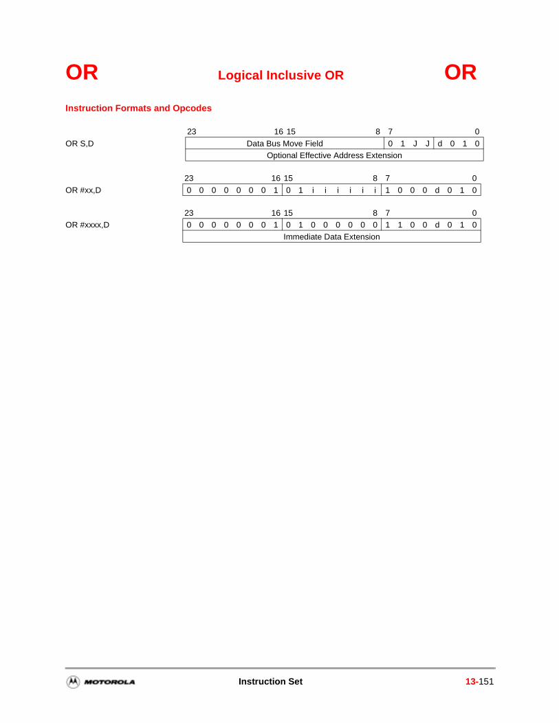
OR Logical Inclusive OR ORInstruction Formats and Opcodes
23 16 15 8 7 0
OR S,D Data Bus Move Field 0 1 J J d 0 1 0Optional Effective Address Extension
23 16 15 8 7 0
OR #xx,D 0 0 0 0 0 0 0 1 0 1 i i i i i i 1 0 0 0 d 0 1 0
23 16 15 8 7 0OR #xxxx,D 0 0 0 0 0 0 0 1 0 1 0 0 0 0 0 0 1 1 0 0 d 0 1 0
Immediate Data Extension
Instruction Set 13-151
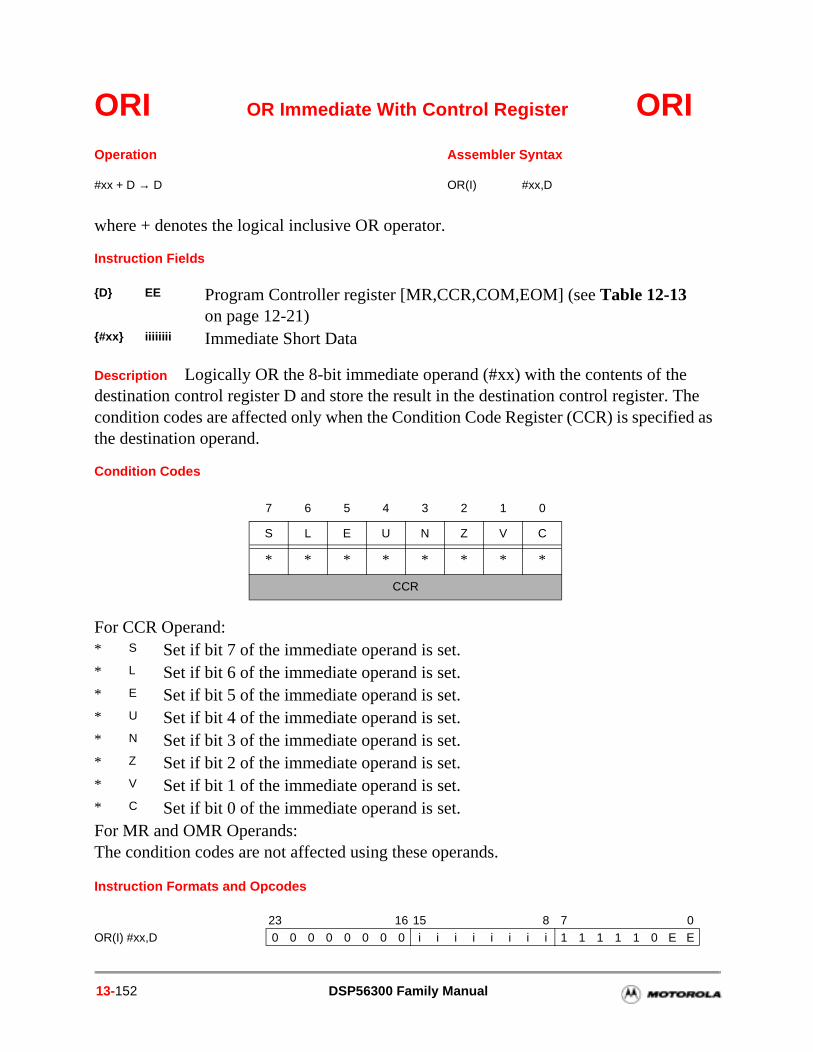
ORI OR Immediate With Control Register ORI
where + denotes the logical inclusive OR operator.
Instruction Fields
Description Logically OR the 8-bit immediate operand (#xx) with the contents of the destination control register D and store the result in the destination control register. The condition codes are affected only when the Condition Code Register (CCR) is specified as the destination operand.
Condition Codes
Instruction Formats and Opcodes
Operation Assembler Syntax
#xx + D → D OR(I) #xx,D
D EE Program Controller register [MR,CCR,COM,EOM] (see Table 12-13 on page 12-21)
#xx iiiiiiii Immediate Short Data
7 6 5 4 3 2 1 0
S L E U N Z V C
* * * * * * * *
CCR
For CCR Operand:* S Set if bit 7 of the immediate operand is set.* L Set if bit 6 of the immediate operand is set.* E Set if bit 5 of the immediate operand is set.* U Set if bit 4 of the immediate operand is set.* N Set if bit 3 of the immediate operand is set.* Z Set if bit 2 of the immediate operand is set.* V Set if bit 1 of the immediate operand is set.* C Set if bit 0 of the immediate operand is set.For MR and OMR Operands: The condition codes are not affected using these operands.
23 16 15 8 7 0OR(I) #xx,D 0 0 0 0 0 0 0 0 i i i i i i i i 1 1 1 1 1 0 E E
13-152 DSP56300 Family Manual
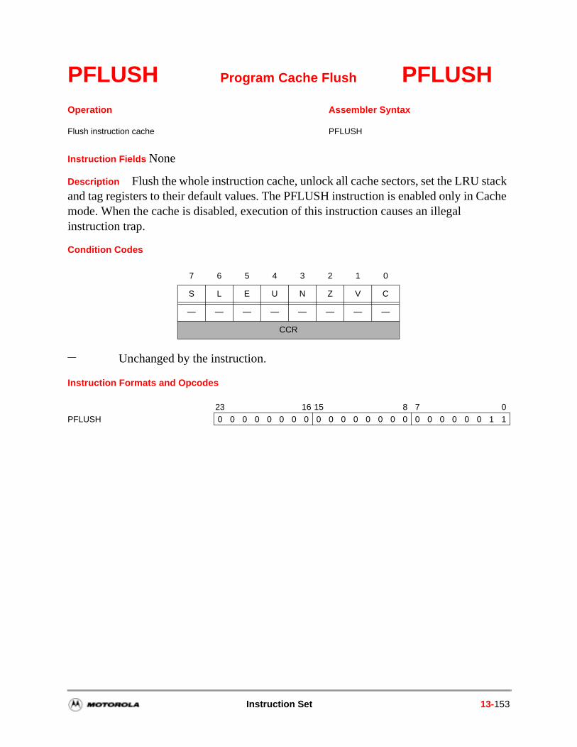
PFLUSH Program Cache Flush PFLUSH
Instruction Fields None
Description Flush the whole instruction cache, unlock all cache sectors, set the LRU stack and tag registers to their default values. The PFLUSH instruction is enabled only in Cache mode. When the cache is disabled, execution of this instruction causes an illegal instruction trap.
Condition Codes
Instruction Formats and Opcodes
Operation Assembler Syntax
Flush instruction cache PFLUSH
7 6 5 4 3 2 1 0
S L E U N Z V C
— — — — — — — —
CCR
— Unchanged by the instruction.
23 16 15 8 7 0PFLUSH 0 0 0 0 0 0 0 0 0 0 0 0 0 0 0 0 0 0 0 0 0 0 1 1
Instruction Set 13-153
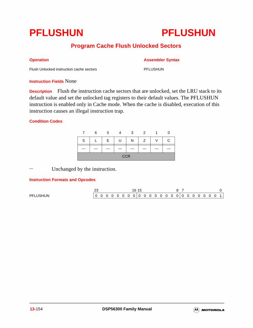
PFLUSHUN PFLUSHUNProgram Cache Flush Unlocked Sectors
Instruction Fields None
Description Flush the instruction cache sectors that are unlocked, set the LRU stack to its default value and set the unlocked tag registers to their default values. The PFLUSHUN instruction is enabled only in Cache mode. When the cache is disabled, execution of this instruction causes an illegal instruction trap.
Condition Codes
Instruction Formats and Opcodes
Operation Assembler Syntax
Flush Unlocked instruction cache sectors PFLUSHUN
7 6 5 4 3 2 1 0
S L E U N Z V C
— — — — — — — —
CCR
— Unchanged by the instruction.
23 16 15 8 7 0
PFLUSHUN 0 0 0 0 0 0 0 0 0 0 0 0 0 0 0 0 0 0 0 0 0 0 0 1
13-154 DSP56300 Family Manual
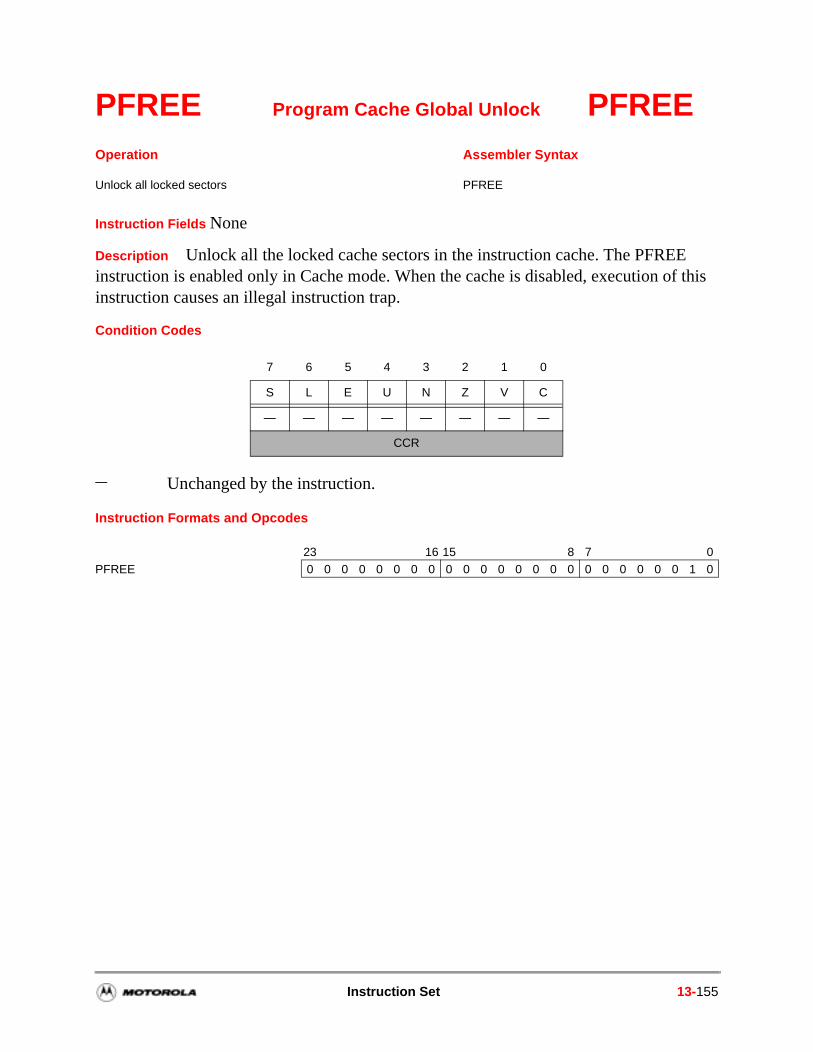
PFREE Program Cache Global Unlock PFREE
Instruction Fields None
Description Unlock all the locked cache sectors in the instruction cache. The PFREE instruction is enabled only in Cache mode. When the cache is disabled, execution of this instruction causes an illegal instruction trap.
Condition Codes
Instruction Formats and Opcodes
Operation Assembler Syntax
Unlock all locked sectors PFREE
7 6 5 4 3 2 1 0
S L E U N Z V C
— — — — — — — —
CCR
— Unchanged by the instruction.
23 16 15 8 7 0PFREE 0 0 0 0 0 0 0 0 0 0 0 0 0 0 0 0 0 0 0 0 0 0 1 0
Instruction Set 13-155
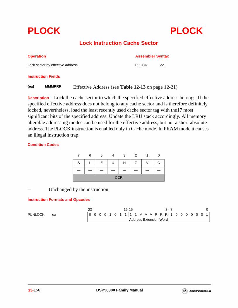
PLOCK PLOCKLock Instruction Cache Sector
Instruction Fields
Description Lock the cache sector to which the specified effective address belongs. If the specified effective address does not belong to any cache sector and is therefore definitely locked, nevertheless, load the least recently used cache sector tag with the17 most significant bits of the specified address. Update the LRU stack accordingly. All memory alterable addressing modes can be used for the effective address, but not a short absolute address. The PLOCK instruction is enabled only in Cache mode. In PRAM mode it causes an illegal instruction trap.
Condition Codes
Instruction Formats and Opcodes
Operation Assembler Syntax
Lock sector by effective address PLOCK ea
ea MMMRRR Effective Address (see Table 12-13 on page 12-21)
7 6 5 4 3 2 1 0
S L E U N Z V C
— — — — — — — —
CCR
— Unchanged by the instruction.
23 16 15 8 7 0PUNLOCK ea 0 0 0 0 1 0 1 1 1 1 M M M R R R 1 0 0 0 0 0 0 1
Address Extension Word
13-156 DSP56300 Family Manual
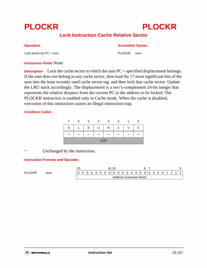
hat e
PLOCKR PLOCKRLock Instruction Cache Relative Sector
Instruction Fields None
Description Lock the cache sector to which the sum PC + specified displacement belongs. If the sum does not belong to any cache sector, then load the 17 most significant bits of the sum into the least recently used cache sector tag, and then lock that cache sector. Update the LRU stack accordingly. The displacement is a two’s-complement 24-bit integer trepresents the relative distance from the current PC to the address to be locked. ThPLOCKR instruction is enabled only in Cache mode. When the cache is disabled, execution of this instruction causes an illegal instruction trap.
Condition Codes
Instruction Formats and Opcodes
Operation Assembler Syntax
Lock sector by PC + xxxx PLOCKR xxxx
7 6 5 4 3 2 1 0
S L E U N Z V C
— — — — — — — —
CCR
— Unchanged by the instruction.
23 16 15 8 7 0PLOCKR xxxx 0 0 0 0 0 0 0 0 0 0 0 0 0 0 0 0 0 0 0 0 1 1 1 1
Address Extension Word
Instruction Set 13-157
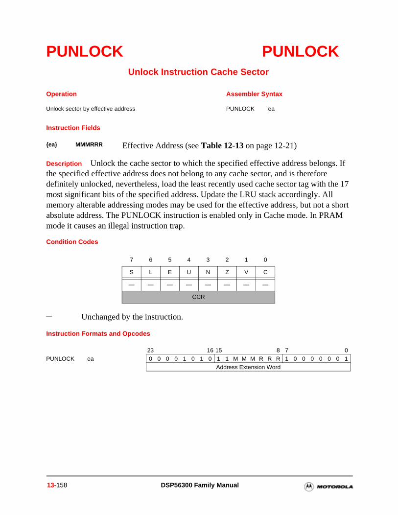
PUNLOCK PUNLOCKUnlock Instruction Cache Sector
Instruction Fields
Description Unlock the cache sector to which the specified effective address belongs. If the specified effective address does not belong to any cache sector, and is therefore definitely unlocked, nevertheless, load the least recently used cache sector tag with the 17 most significant bits of the specified address. Update the LRU stack accordingly. All memory alterable addressing modes may be used for the effective address, but not a short absolute address. The PUNLOCK instruction is enabled only in Cache mode. In PRAM mode it causes an illegal instruction trap.
Condition Codes
Instruction Formats and Opcodes
Operation Assembler Syntax
Unlock sector by effective address PUNLOCK ea
ea MMMRRR Effective Address (see Table 12-13 on page 12-21)
7 6 5 4 3 2 1 0
S L E U N Z V C
— — — — — — — —
CCR
— Unchanged by the instruction.
23 16 15 8 7 0PUNLOCK ea 0 0 0 0 1 0 1 0 1 1 M M M R R R 1 0 0 0 0 0 0 1
Address Extension Word
13-158 DSP56300 Family Manual
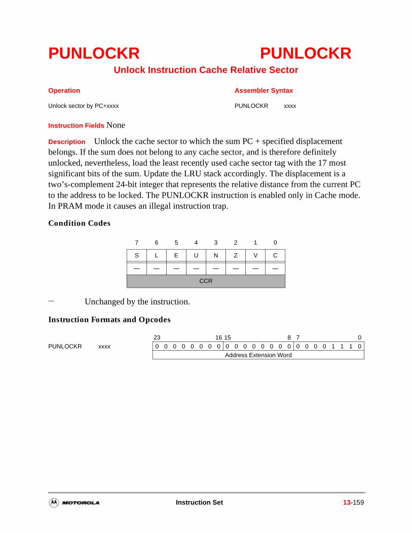
nt PC ode.
PUNLOCKR PUNLOCKRUnlock Instruction Cache Relative Sector
Instruction Fields None
Description Unlock the cache sector to which the sum PC + specified displacement belongs. If the sum does not belong to any cache sector, and is therefore definitely unlocked, nevertheless, load the least recently used cache sector tag with the 17 most significant bits of the sum. Update the LRU stack accordingly. The displacement is a two’s-complement 24-bit integer that represents the relative distance from the curreto the address to be locked. The PUNLOCKR instruction is enabled only in Cache mIn PRAM mode it causes an illegal instruction trap.
Condition Codes
Instruction Formats and Opcodes
Operation Assembler Syntax
Unlock sector by PC+xxxx PUNLOCKR xxxx
7 6 5 4 3 2 1 0
S L E U N Z V C
— — — — — — — —
CCR
— Unchanged by the instruction.
23 16 15 8 7 0
PUNLOCKR xxxx 0 0 0 0 0 0 0 0 0 0 0 0 0 0 0 0 0 0 0 0 1 1 1 0Address Extension Word
Instruction Set 13-159
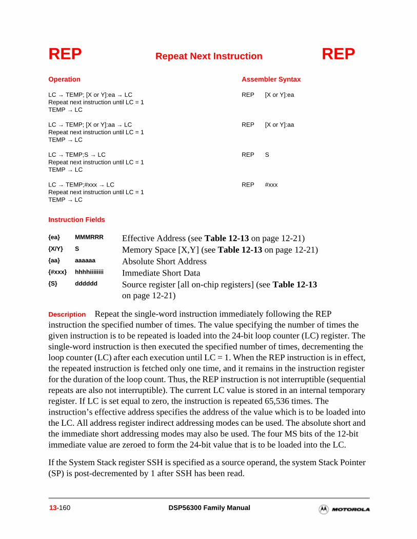
d into ort and 2-bit
Pointer
REP Repeat Next Instruction REP
Instruction Fields
Description Repeat the single-word instruction immediately following the REP instruction the specified number of times. The value specifying the number of times the given instruction is to be repeated is loaded into the 24-bit loop counter (LC) register. The single-word instruction is then executed the specified number of times, decrementing the loop counter (LC) after each execution until LC = 1. When the REP instruction is in effect, the repeated instruction is fetched only one time, and it remains in the instruction register for the duration of the loop count. Thus, the REP instruction is not interruptible (sequential repeats are also not interruptible). The current LC value is stored in an internal temporary register. If LC is set equal to zero, the instruction is repeated 65,536 times. The instruction’s effective address specifies the address of the value which is to be loadethe LC. All address register indirect addressing modes can be used. The absolute shthe immediate short addressing modes may also be used. The four MS bits of the 1immediate value are zeroed to form the 24-bit value that is to be loaded into the LC.
If the System Stack register SSH is specified as a source operand, the system Stack(SP) is post-decremented by 1 after SSH has been read.
Operation Assembler Syntax
LC → TEMP; [X or Y]:ea → LC REP [X or Y]:eaRepeat next instruction until LC = 1TEMP → LC
LC → TEMP; [X or Y]:aa → LC REP [X or Y]:aaRepeat next instruction until LC = 1TEMP → LC
LC → TEMP;S → LC REP SRepeat next instruction until LC = 1TEMP → LC
LC → TEMP;#xxx → LC REP #xxxRepeat next instruction until LC = 1TEMP → LC
ea MMMRRR Effective Address (see Table 12-13 on page 12-21)X/Y S Memory Space [X,Y] (see Table 12-13 on page 12-21)aa aaaaaa Absolute Short Address#xxx hhhhiiiiiiii Immediate Short DataS dddddd Source register [all on-chip registers] (see Table 12-13
on page 12-21)
13-160 DSP56300 Family Manual
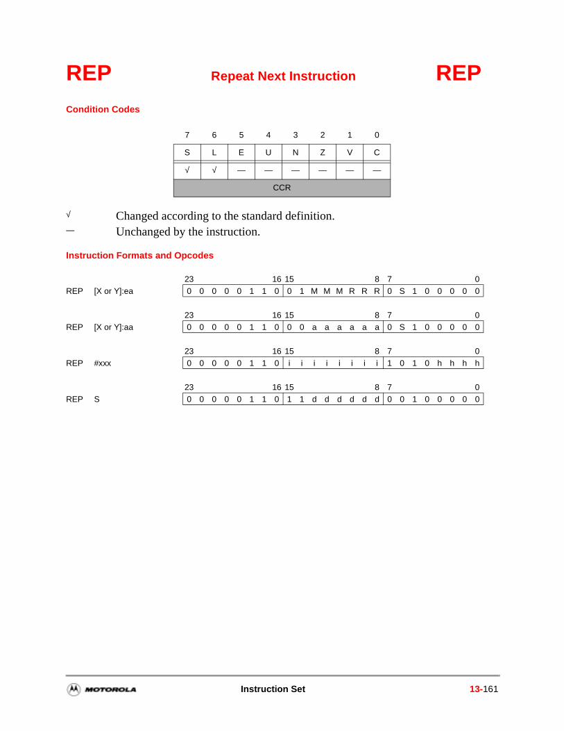
REP Repeat Next Instruction REPCondition Codes
Instruction Formats and Opcodes
7 6 5 4 3 2 1 0
S L E U N Z V C
√ √ — — — — — —
CCR
√ Changed according to the standard definition.— Unchanged by the instruction.
23 16 15 8 7 0REP [X or Y]:ea 0 0 0 0 0 1 1 0 0 1 M M M R R R 0 S 1 0 0 0 0 0
23 16 15 8 7 0REP [X or Y]:aa 0 0 0 0 0 1 1 0 0 0 a a a a a a 0 S 1 0 0 0 0 0
23 16 15 8 7 0REP #xxx 0 0 0 0 0 1 1 0 i i i i i i i i 1 0 1 0 h h h h
23 16 15 8 7 0REP S 0 0 0 0 0 1 1 0 1 1 d d d d d d 0 0 1 0 0 0 0 0
Instruction Set 13-161
RESET Reset On-Chip Peripheral Devices RESET
Instruction Fields None
Description Reset the interrupt priority register and all on-chip peripherals. This is a software reset, which is not equivalent to a hardware RESET since only on-chip peripherals and the interrupt structure are affected. The processor state is not affected, and execution continues with the next instruction. All interrupt sources are disabled except for the stack error, NMI, illegal instruction, Trap, Debug request, and hardware reset interrupts.
Condition Codes
Instruction Formats and Opcodes
Operation Assembler Syntax
Reset the interrupt priority register and all on-chip peripherals
RESET
7 6 5 4 3 2 1 0
S L E U N Z V C
— — — — — — — —
CCR
— Unchanged by the instruction.
23 16 15 8 7 0RESET 0 0 0 0 0 0 0 0 0 0 0 0 0 0 0 0 1 0 0 0 0 1 0 0
13-162 DSP56300 Family Manual
ding tant
nding nt ble
f the the t ared. gister ult.
is
RND Round Accumulator RND
Instruction Fields
Description Round the 56-bit value in the specified destination operand D and store the result in the destination accumulator (A or B). The contribution of the LSBs of the operand is rounded into the upper portion of the operand by adding a rounding constant to the LSBs of the operand. The upper portion of the destination accumulator contains the rounded result. The boundary between the lower portion and the upper portion is determined by the scaling mode bits S0 and S1 in the Status Register (SR).
Two types of rounding can be used: convergent rounding (also called round to nearest (even)) or two’s-complement rounding. The type of rounding is selected by the RounMode bit (RM) in the MR portion of the SR. In both rounding modes a rounding consis first added to the unrounded result. The value of the rounding constant added is determined by the scaling mode bits S0 and S1 in the SR. A 1 is positioned in the rouconstant aligned with the MSB of the current LS portion, that is, the rounding constaweight is actually equal to half the weight of the upper portion’s LSB. The following tashows the rounding position and rounding constant as determined by the scaling mode bits:
If convergent rounding is used, the result of this addition is tested and if all the bits oresult to the right of, and including, the rounding position are cleared, then the bit to left of the rounding position is cleared in the result. This ensures that the result is nobiased. In both rounding modes, the Least Significant Bits (LSBs) of the result are cleThe number of LSBs cleared is determined by the Scaling Mode bits in the Status Re(SR). All bits to the right of and including the rounding position are cleared in the res
In Sixteen-bit Arithmetic mode the 40-bit value (in the 56-bit destination operand D) rounded and stored in the destination accumulator (A or B). This implies that the
Operation Assembler Syntax
D + r → D (parallel move) RND D (parallel move)
D d Destination accumulator [A,B] (see Table 12-13 on page 12-21)
Rounding Rounding Constant
S1 S0 Scaling Mode Position 55–25 24 23 22 21–0
0 0 No Scaling 23 0. . . .0 0 1 0 0. . . .0
0 1 Scale Down 24 0. . . .0 1 0 0 0. . . .0
1 0 Scale Up 22 0. . . .0 0 0 1 0. . . .0
Instruction Set 13-163
RND Round Accumulator RND
boundary between the lower portion and upper portion is in a different position then in 24 bit mode. The following table shows the rounding position and rounding constant in Sixteen-bit Arithmetic mode, as determined by the scaling mode bits:
Condition Codes
Instruction Formats and Opcodes
7 6 5 4 3 2 1 0
S L E U N Z V C
√ √ √ √ √ √ √ —
CCR
√ Changed according to the standard definition. — Unchanged by the instruction.
23 16 15 8 7 0
RND D Data Bus Move Field 0 0 0 1 d 0 0 1Optional Effective Address Extension
Rounding Rounding Constant
S1 S0 Scaling Mode Position 55–33 32 23 22 21–8
0 0 No Scaling 31 0. . . .0 0 1 0 0. . . .0
0 1 Scale Down 32 0. . . .0 1 0 0 0. . . .0
1 0 Scale Up 30 0. . . .0 0 0 1 0. . . .0
13-164 DSP56300 Family Manual
the f bit d. e not
ROL Rotate Left ROLOperation
Assembler Syntax
ROL D (parallel move)
Instruction Fields
Description Rotate bits 47–24 of the destination operand D one bit to the left and storeresult in the destination accumulator. The Carry bit (C) receives the previous value o47 of the operand. The previous value of the C bit is shifted into bit 24 of the operanThis instruction is a 24-bit operation. The remaining bits of destination operand D araffected.
Condition Codes
Instruction Formats and Opcodes
D d Destination accumulator [A,B] (see Table 12-13 on page 12-21)
7 6 5 4 3 2 1 0
S L E U N Z V C
√ √ — — * * * *
CCR
* N Set if bit 47 of the result is set. * Z Set if bits 47–24 of the result are 0. * V This bit is always cleared. * C Set if bit 47 of the destination operand is set, and cleared otherwise.√ Changed according to the standard definition. — Unchanged by the instruction.
23 16 15 8 7 0
ROL D Data Bus Move Field 0 0 1 1 d 1 1 1Optional Effective Address Extension
C
47 24
Instruction Set 13-165
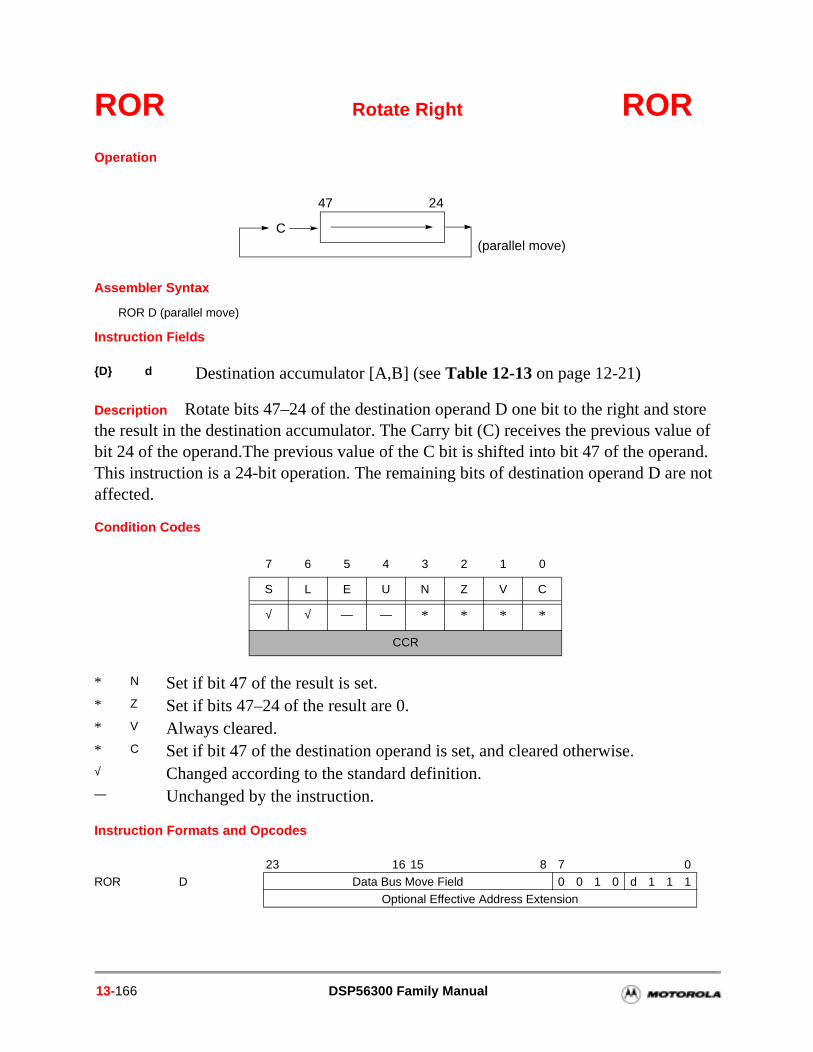
re ue of and. e not
ROR Rotate Right ROROperation
Assembler Syntax
ROR D (parallel move)
Instruction Fields
Description Rotate bits 47–24 of the destination operand D one bit to the right and stothe result in the destination accumulator. The Carry bit (C) receives the previous valbit 24 of the operand.The previous value of the C bit is shifted into bit 47 of the operThis instruction is a 24-bit operation. The remaining bits of destination operand D araffected.
Condition Codes
Instruction Formats and Opcodes
D d Destination accumulator [A,B] (see Table 12-13 on page 12-21)
7 6 5 4 3 2 1 0
S L E U N Z V C
√ √ — — * * * *
CCR
* N Set if bit 47 of the result is set. * Z Set if bits 47–24 of the result are 0. * V Always cleared. * C Set if bit 47 of the destination operand is set, and cleared otherwise.√ Changed according to the standard definition. — Unchanged by the instruction.
23 16 15 8 7 0ROR D Data Bus Move Field 0 0 1 0 d 1 1 1
Optional Effective Address Extension
C
47
(parallel move)
24
13-166 DSP56300 Family Manual
RTI Return From Interrupt RTI
Instruction Fields None
Description Pull the Program Counter (PC) and the Status Register (SR) from the system stack. The previous PC and SR values are lost.
Condition Codes
Instruction Formats and Opcodes
Operation Assembler Syntax
SSH → PC; SSL → SR; SP – 1 → SP RTI
7 6 5 4 3 2 1 0
S L E U N Z V C
* * * * * * * *
CCR
* S Set according to the value pulled from the stack. * L Set according to the value pulled from the stack. * E Set according to the value pulled from the stack. * U Set according to the value pulled from the stack. * N Set according to the value pulled from the stack. * Z Set according to the value pulled from the stack. * V Set according to the value pulled from the stack. * C Set according to the value pulled from the stack.
23 16 15 8 7 0RTI 0 0 0 0 0 0 0 0 0 0 0 0 0 0 0 0 0 0 0 0 0 1 0 0
Instruction Set 13-167
RTS Return From Subroutine RTS
Instruction Fields None
Description Pull the Program Counter (PC) from the system stack. The previous PC value is lost. The Status Register (SR) is not affected.
Condition Codes
Instruction Formats and Opcodes
Operation Assembler Syntax
SSH → PC; SP – 1 → SP RTS
7 6 5 4 3 2 1 0
S L E U N Z V C
— — — — — — — —
CCR
— Unchanged by the instruction.
23 16 15 8 7 0
RTS 0 0 0 0 0 0 0 0 0 0 0 0 0 0 0 0 0 0 0 0 1 1 0 0
13-168 DSP56300 Family Manual
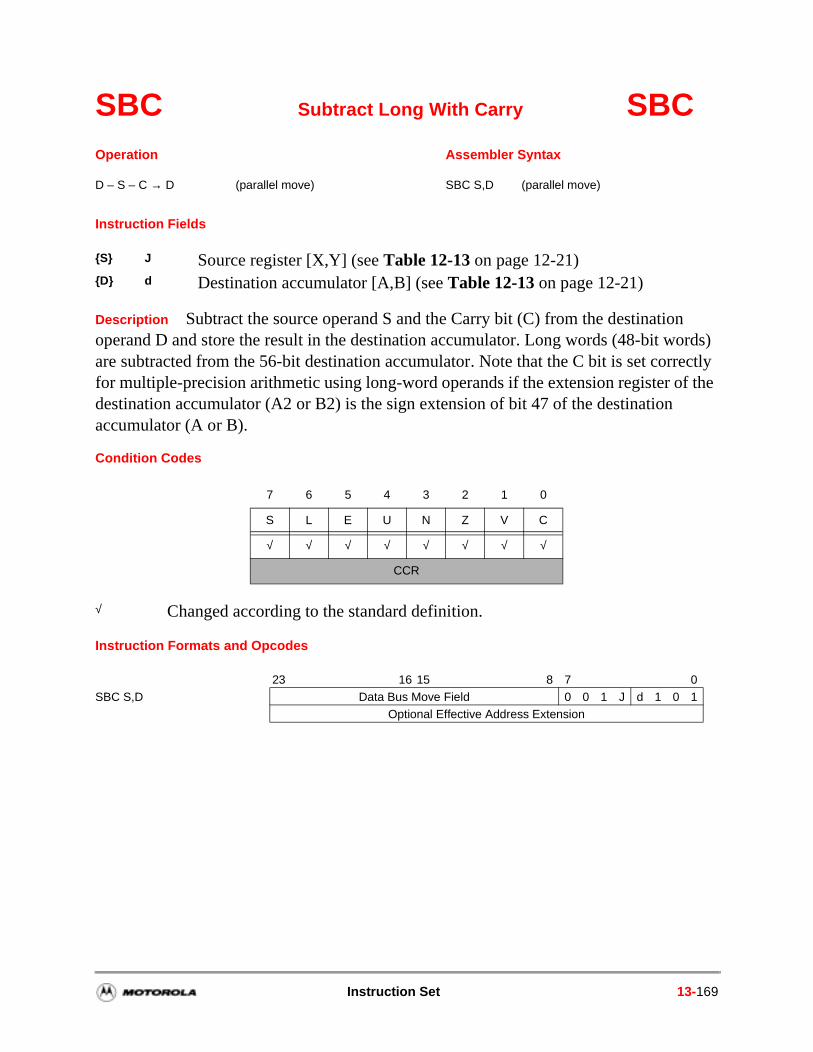
SBC Subtract Long With Carry SBC
Instruction Fields
Description Subtract the source operand S and the Carry bit (C) from the destination operand D and store the result in the destination accumulator. Long words (48-bit words) are subtracted from the 56-bit destination accumulator. Note that the C bit is set correctly for multiple-precision arithmetic using long-word operands if the extension register of the destination accumulator (A2 or B2) is the sign extension of bit 47 of the destination accumulator (A or B).
Condition Codes
Instruction Formats and Opcodes
Operation Assembler Syntax
D – S – C → D (parallel move) SBC S,D (parallel move)
S J Source register [X,Y] (see Table 12-13 on page 12-21)D d Destination accumulator [A,B] (see Table 12-13 on page 12-21)
7 6 5 4 3 2 1 0
S L E U N Z V C
√ √ √ √ √ √ √ √
CCR
√ Changed according to the standard definition.
23 16 15 8 7 0SBC S,D Data Bus Move Field 0 0 1 J d 1 0 1
Optional Effective Address Extension
Instruction Set 13-169
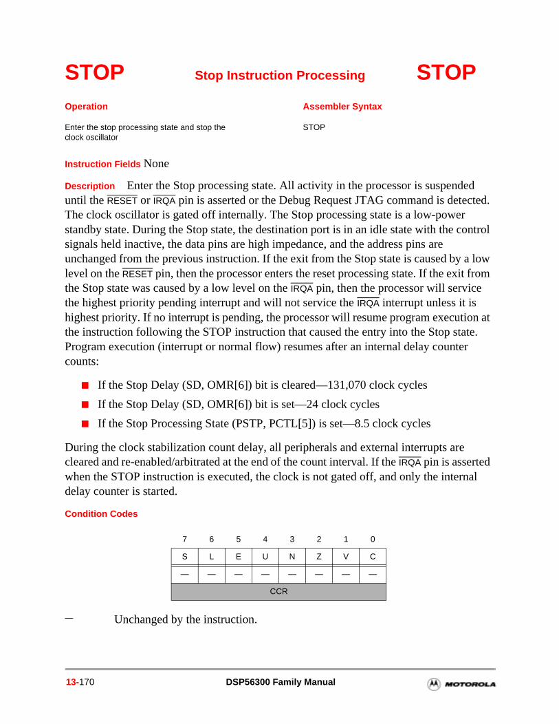
nal
STOP Stop Instruction Processing STOP
Instruction Fields None
Description Enter the Stop processing state. All activity in the processor is suspended until the RESET or IRQA pin is asserted or the Debug Request JTAG command is detected. The clock oscillator is gated off internally. The Stop processing state is a low-power standby state. During the Stop state, the destination port is in an idle state with the control signals held inactive, the data pins are high impedance, and the address pins are unchanged from the previous instruction. If the exit from the Stop state is caused by a low level on the RESET pin, then the processor enters the reset processing state. If the exit from the Stop state was caused by a low level on the IRQA pin, then the processor will service the highest priority pending interrupt and will not service the IRQA interrupt unless it is highest priority. If no interrupt is pending, the processor will resume program execution at the instruction following the STOP instruction that caused the entry into the Stop state. Program execution (interrupt or normal flow) resumes after an internal delay counter counts:
If the Stop Delay (SD, OMR[6]) bit is cleared—131,070 clock cycles
If the Stop Delay (SD, OMR[6]) bit is set—24 clock cycles
If the Stop Processing State (PSTP, PCTL[5]) is set—8.5 clock cycles
During the clock stabilization count delay, all peripherals and external interrupts arecleared and re-enabled/arbitrated at the end of the count interval. If the IRQA pin is asserted when the STOP instruction is executed, the clock is not gated off, and only the interdelay counter is started.
Condition Codes
Operation Assembler Syntax
Enter the stop processing state and stop the clock oscillator
STOP
7 6 5 4 3 2 1 0
S L E U N Z V C
— — — — — — — —
CCR
— Unchanged by the instruction.
13-170 DSP56300 Family Manual
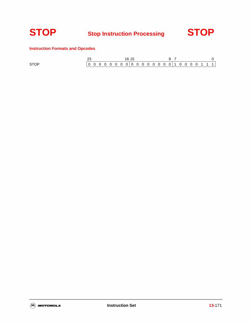
STOP Stop Instruction Processing STOPInstruction Formats and Opcodes
23 16 15 8 7 0
STOP 0 0 0 0 0 0 0 0 0 0 0 0 0 0 0 0 1 0 0 0 0 1 1 1
Instruction Set 13-171
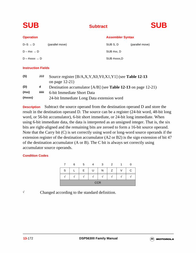
SUB Subtract SUB
Instruction Fields
Description Subtract the source operand from the destination operand D and store the result in the destination operand D. The source can be a register (24-bit word, 48-bit long word, or 56-bit accumulator), 6-bit short immediate, or 24-bit long immediate. When using 6-bit immediate data, the data is interpreted as an unsigned integer. That is, the six bits are right-aligned and the remaining bits are zeroed to form a 16-bit source operand. Note that the Carry bit (C) is set correctly using word or long-word source operands if the extension register of the destination accumulator (A2 or B2) is the sign extension of bit 47 of the destination accumulator (A or B). The C bit is always set correctly using accumulator source operands.
Condition Codes
Operation Assembler Syntax
D–S → D (parallel move) SUB S, D (parallel move)
D – #xx → D SUB #xx, D
D – #xxxx → D SUB #xxxx,D
S JJJ Source register [B/A,X,Y,X0,Y0,X1,Y1] (see Table 12-13 on page 12-21)
D d Destination accumulator [A/B] (see Table 12-13 on page 12-21)#xx iiiiii 6-bit Immediate Short Data #xxxx 24-bit Immediate Long Data extension word
7 6 5 4 3 2 1 0
S L E U N Z V C
√ √ √ √ √ √ √ √
CCR
√ Changed according to the standard definition.
13-172 DSP56300 Family Manual
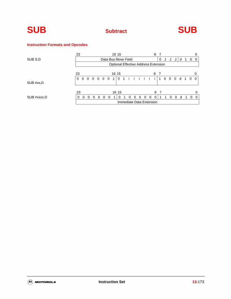
SUB Subtract SUBInstruction Formats and Opcodes
23 16 15 8 7 0
SUB S,D Data Bus Move Field 0 J J J d 1 0 0Optional Effective Address Extension
23 16 15 8 7 0
SUB #xx,D0 0 0 0 0 0 0 1 0 1 i i i i i i 1 0 0 0 d 1 0 0
23 16 15 8 7 0SUB #xxxx,D 0 0 0 0 0 0 0 1 0 1 0 0 0 0 0 0 1 1 0 0 d 1 0 0
Immediate Data Extension
Instruction Set 13-173
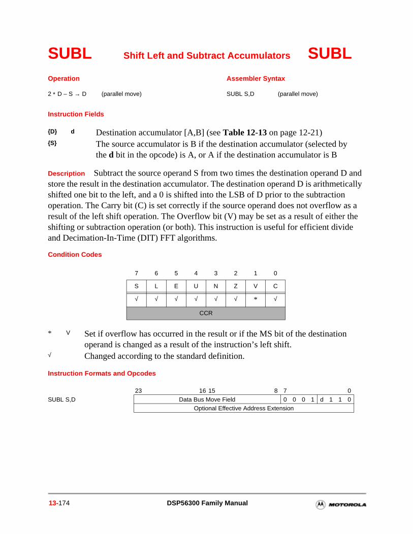
SUBL Shift Left and Subtract Accumulators SUBL
Instruction Fields
Description Subtract the source operand S from two times the destination operand D and store the result in the destination accumulator. The destination operand D is arithmetically shifted one bit to the left, and a 0 is shifted into the LSB of D prior to the subtraction operation. The Carry bit (C) is set correctly if the source operand does not overflow as a result of the left shift operation. The Overflow bit (V) may be set as a result of either the shifting or subtraction operation (or both). This instruction is useful for efficient divide and Decimation-In-Time (DIT) FFT algorithms.
Condition Codes
Instruction Formats and Opcodes
Operation Assembler Syntax
2 ∗ D – S → D (parallel move) SUBL S,D (parallel move)
D d Destination accumulator [A,B] (see Table 12-13 on page 12-21)S The source accumulator is B if the destination accumulator (selected by
the d bit in the opcode) is A, or A if the destination accumulator is B
7 6 5 4 3 2 1 0
S L E U N Z V C
√ √ √ √ √ √ * √
CCR
* V Set if overflow has occurred in the result or if the MS bit of the destination operand is changed as a result of the instruction’s left shift.
√ Changed according to the standard definition.
23 16 15 8 7 0
SUBL S,D Data Bus Move Field 0 0 0 1 d 1 1 0Optional Effective Address Extension
13-174 DSP56300 Family Manual
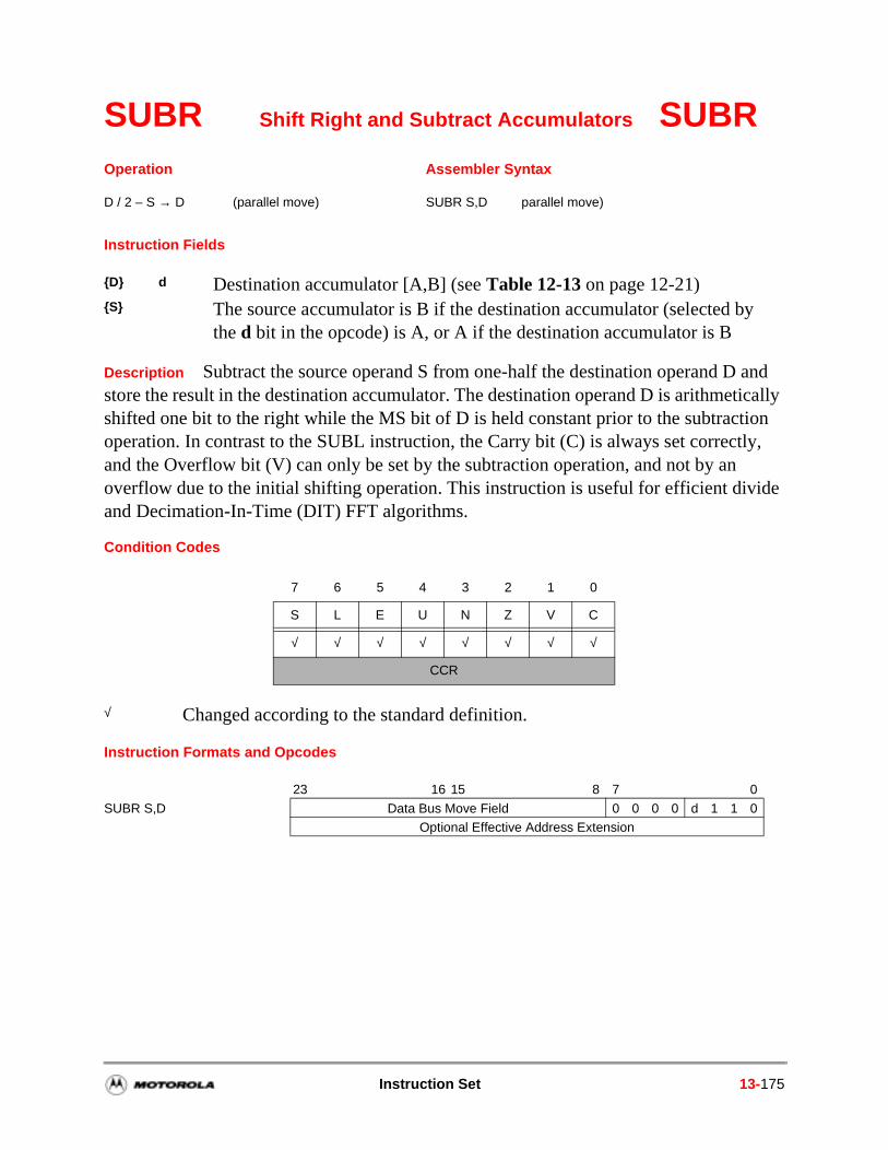
SUBR Shift Right and Subtract Accumulators SUBR
Instruction Fields
Description Subtract the source operand S from one-half the destination operand D and store the result in the destination accumulator. The destination operand D is arithmetically shifted one bit to the right while the MS bit of D is held constant prior to the subtraction operation. In contrast to the SUBL instruction, the Carry bit (C) is always set correctly, and the Overflow bit (V) can only be set by the subtraction operation, and not by an overflow due to the initial shifting operation. This instruction is useful for efficient divide and Decimation-In-Time (DIT) FFT algorithms.
Condition Codes
Instruction Formats and Opcodes
Operation Assembler Syntax
D / 2 – S → D (parallel move) SUBR S,D parallel move)
D d Destination accumulator [A,B] (see Table 12-13 on page 12-21)S The source accumulator is B if the destination accumulator (selected by
the d bit in the opcode) is A, or A if the destination accumulator is B
7 6 5 4 3 2 1 0
S L E U N Z V C
√ √ √ √ √ √ √ √
CCR
√ Changed according to the standard definition.
23 16 15 8 7 0
SUBR S,D Data Bus Move Field 0 0 0 0 d 1 1 0Optional Effective Address Extension
Instruction Set 13-175
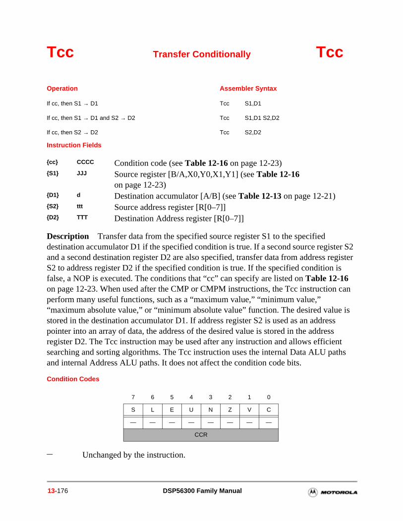
can
is ss s
nt ths
Tcc Transfer Conditionally Tcc
Instruction Fields
Description Transfer data from the specified source register S1 to the specified destination accumulator D1 if the specified condition is true. If a second source register S2 and a second destination register D2 are also specified, transfer data from address register S2 to address register D2 if the specified condition is true. If the specified condition is false, a NOP is executed. The conditions that “cc” can specify are listed on Table 12-16 on page 12-23. When used after the CMP or CMPM instructions, the Tcc instructionperform many useful functions, such as a “maximum value,” “minimum value,” “maximum absolute value,” or “minimum absolute value” function. The desired valuestored in the destination accumulator D1. If address register S2 is used as an addrepointer into an array of data, the address of the desired value is stored in the addresregister D2. The Tcc instruction may be used after any instruction and allows efficiesearching and sorting algorithms. The Tcc instruction uses the internal Data ALU paand internal Address ALU paths. It does not affect the condition code bits.
Condition Codes
Operation Assembler Syntax
If cc, then S1 → D1 Tcc S1,D1
If cc, then S1 → D1 and S2 → D2 Tcc S1,D1 S2,D2
If cc, then S2 → D2 Tcc S2,D2
cc CCCC Condition code (see Table 12-16 on page 12-23)S1 JJJ Source register [B/A,X0,Y0,X1,Y1] (see Table 12-16
on page 12-23)D1 d Destination accumulator [A/B] (see Table 12-13 on page 12-21)S2 ttt Source address register [R[0–7]]D2 TTT Destination Address register [R[0–7]]
7 6 5 4 3 2 1 0
S L E U N Z V C
— — — — — — — —
CCR
— Unchanged by the instruction.
13-176 DSP56300 Family Manual
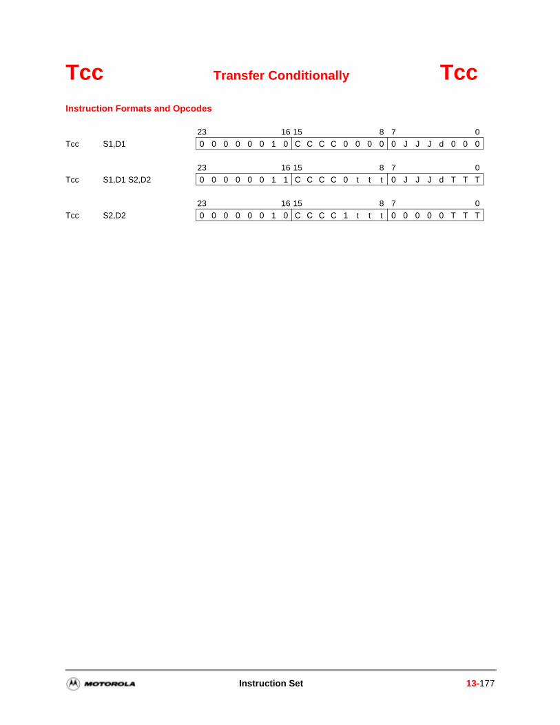
Tcc Transfer Conditionally TccInstruction Formats and Opcodes
23 16 15 8 7 0
Tcc S1,D1 0 0 0 0 0 0 1 0 C C C C 0 0 0 0 0 J J J d 0 0 0
23 16 15 8 7 0
Tcc S1,D1 S2,D2 0 0 0 0 0 0 1 1 C C C C 0 t t t 0 J J J d T T T
23 16 15 8 7 0
Tcc S2,D2 0 0 0 0 0 0 1 0 C C C C 1 t t t 0 0 0 0 0 T T T
Instruction Set 13-177
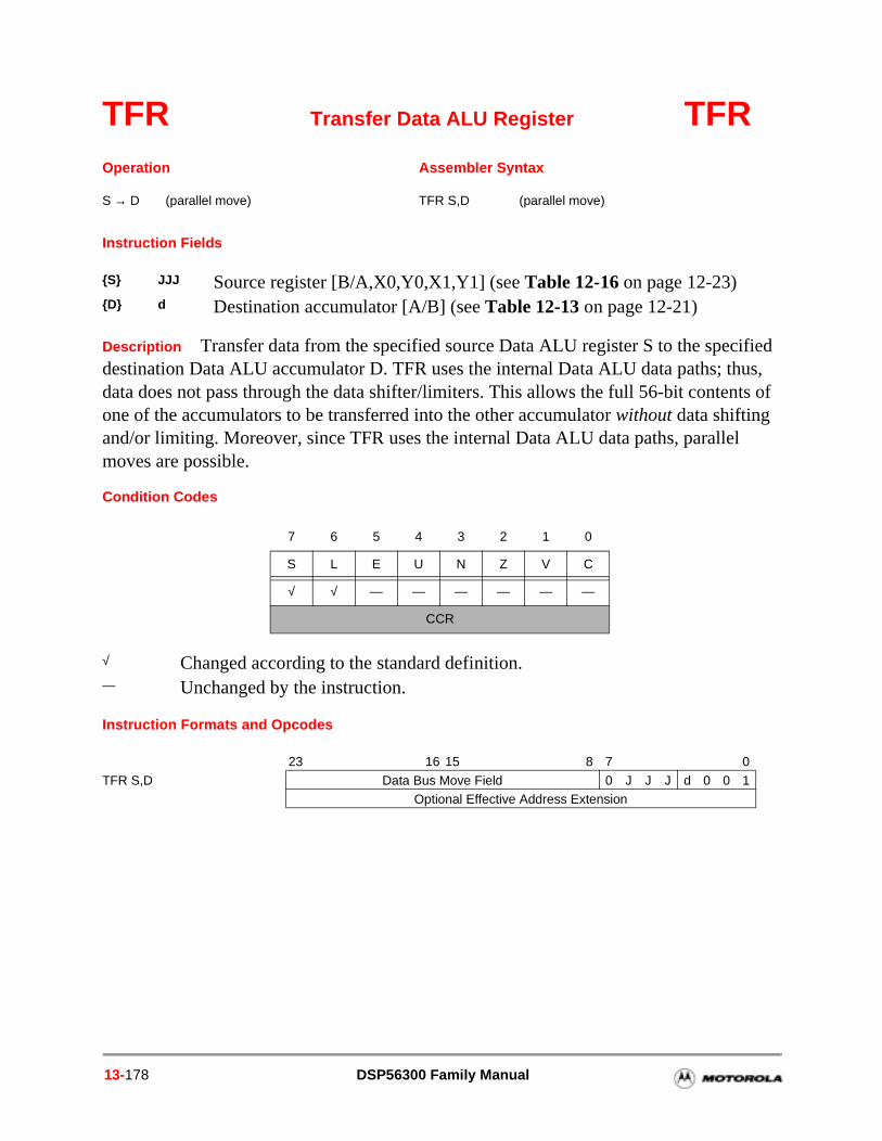
TFR Transfer Data ALU Register TFR
Instruction Fields
Description Transfer data from the specified source Data ALU register S to the specified destination Data ALU accumulator D. TFR uses the internal Data ALU data paths; thus, data does not pass through the data shifter/limiters. This allows the full 56-bit contents of one of the accumulators to be transferred into the other accumulator without data shifting and/or limiting. Moreover, since TFR uses the internal Data ALU data paths, parallel moves are possible.
Condition Codes
Instruction Formats and Opcodes
Operation Assembler Syntax
S → D (parallel move) TFR S,D (parallel move)
S JJJ Source register [B/A,X0,Y0,X1,Y1] (see Table 12-16 on page 12-23)D d Destination accumulator [A/B] (see Table 12-13 on page 12-21)
7 6 5 4 3 2 1 0
S L E U N Z V C
√ √ — — — — — —
CCR
√ Changed according to the standard definition. — Unchanged by the instruction.
23 16 15 8 7 0
TFR S,D Data Bus Move Field 0 J J J d 0 0 1Optional Effective Address Extension
13-178 DSP56300 Family Manual
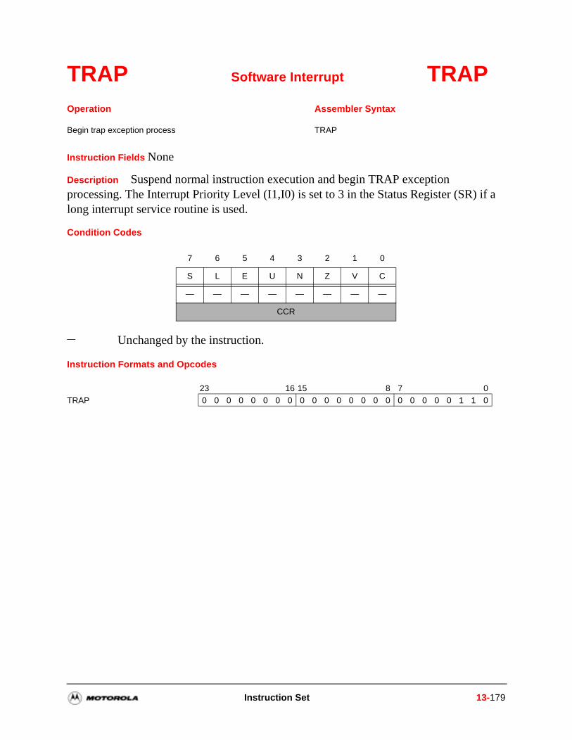
TRAP Software Interrupt TRAP
Instruction Fields None
Description Suspend normal instruction execution and begin TRAP exception processing. The Interrupt Priority Level (I1,I0) is set to 3 in the Status Register (SR) if a long interrupt service routine is used.
Condition Codes
Instruction Formats and Opcodes
Operation Assembler Syntax
Begin trap exception process TRAP
7 6 5 4 3 2 1 0
S L E U N Z V C
— — — — — — — —
CCR
— Unchanged by the instruction.
23 16 15 8 7 0TRAP 0 0 0 0 0 0 0 0 0 0 0 0 0 0 0 0 0 0 0 0 0 1 1 0
Instruction Set 13-179
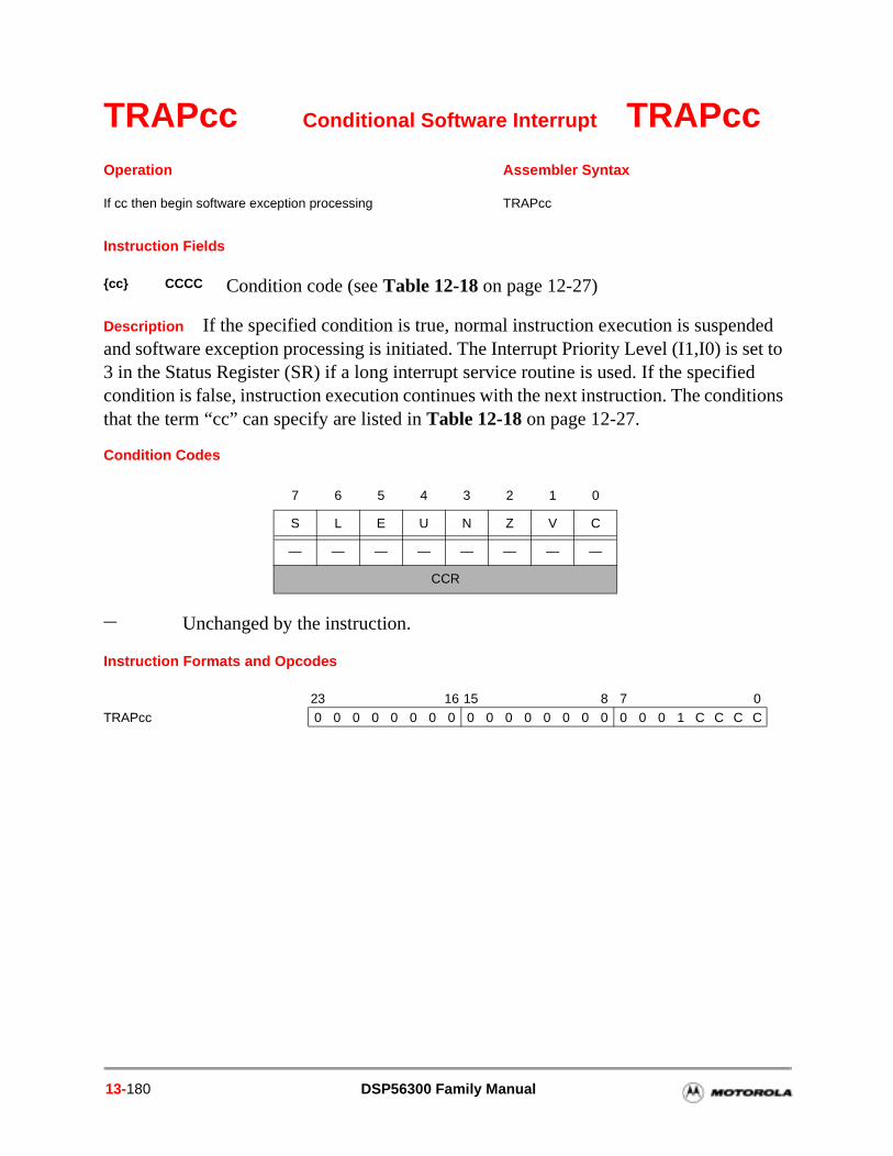
TRAPcc Conditional Software Interrupt TRAPcc
Instruction Fields
Description If the specified condition is true, normal instruction execution is suspended and software exception processing is initiated. The Interrupt Priority Level (I1,I0) is set to 3 in the Status Register (SR) if a long interrupt service routine is used. If the specified condition is false, instruction execution continues with the next instruction. The conditions that the term “cc” can specify are listed in Table 12-18 on page 12-27.
Condition Codes
Instruction Formats and Opcodes
Operation Assembler Syntax
If cc then begin software exception processing TRAPcc
cc CCCC Condition code (see Table 12-18 on page 12-27)
7 6 5 4 3 2 1 0
S L E U N Z V C
— — — — — — — —
CCR
— Unchanged by the instruction.
23 16 15 8 7 0TRAPcc 0 0 0 0 0 0 0 0 0 0 0 0 0 0 0 0 0 0 0 1 C C C C
13-180 DSP56300 Family Manual
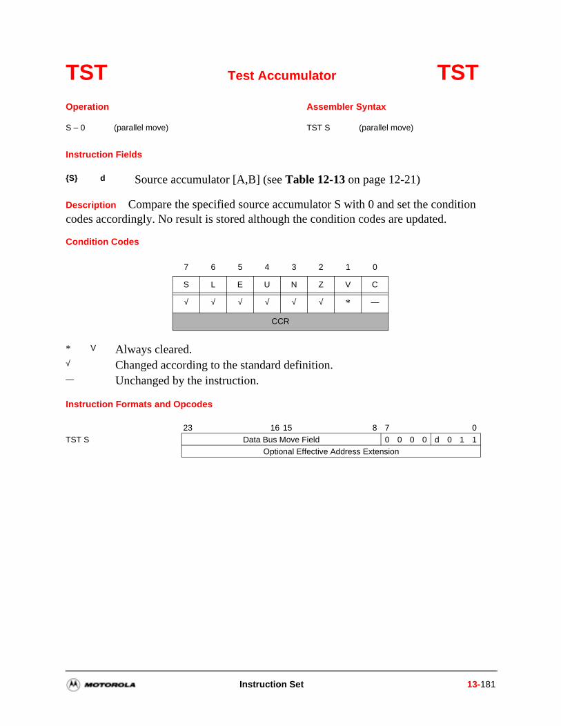
TST Test Accumulator TST
Instruction Fields
Description Compare the specified source accumulator S with 0 and set the condition codes accordingly. No result is stored although the condition codes are updated.
Condition Codes
Instruction Formats and Opcodes
Operation Assembler Syntax
S – 0 (parallel move) TST S (parallel move)
S d Source accumulator [A,B] (see Table 12-13 on page 12-21)
7 6 5 4 3 2 1 0
S L E U N Z V C
√ √ √ √ √ √ * —
CCR
* V Always cleared. √ Changed according to the standard definition. — Unchanged by the instruction.
23 16 15 8 7 0TST S Data Bus Move Field 0 0 0 0 d 0 1 1
Optional Effective Address Extension
Instruction Set 13-181
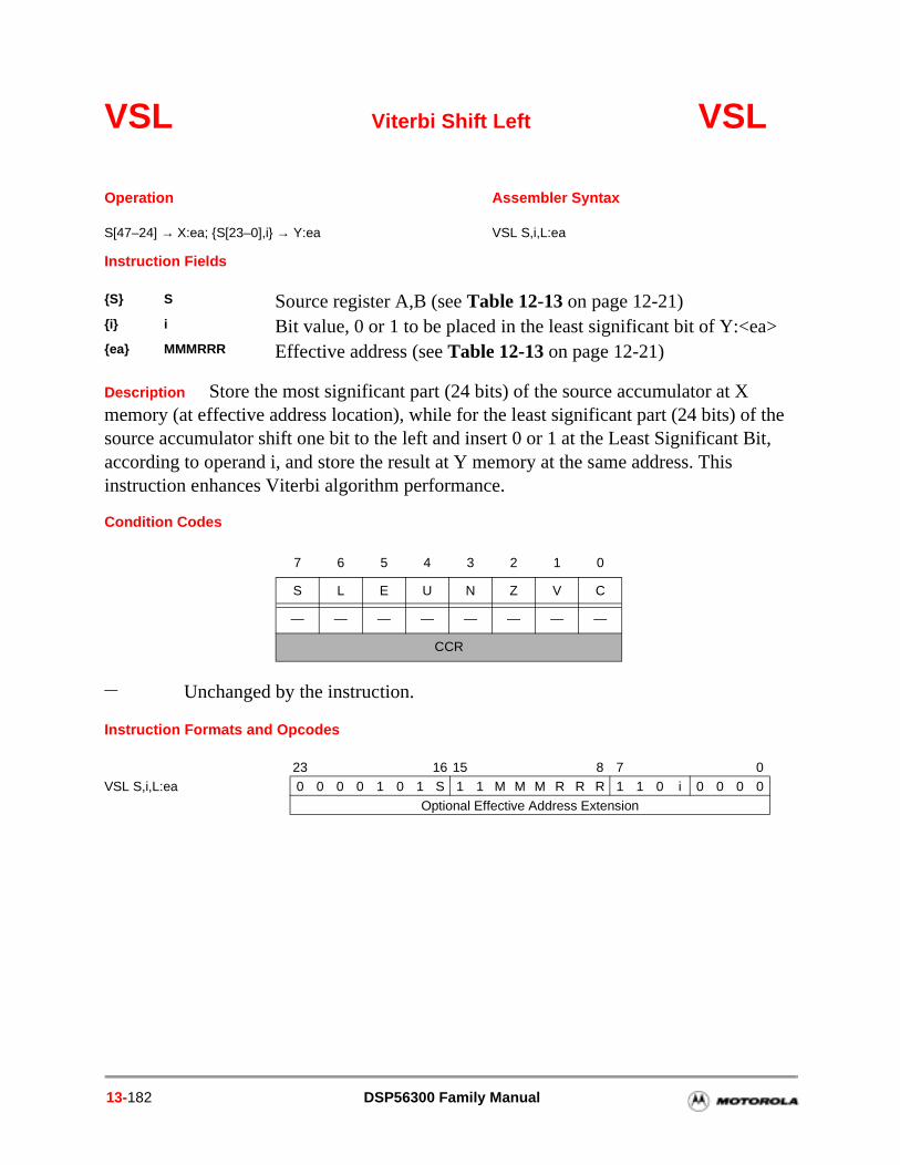
VSL Viterbi Shift Left VSL
Instruction Fields
Description Store the most significant part (24 bits) of the source accumulator at X memory (at effective address location), while for the least significant part (24 bits) of the source accumulator shift one bit to the left and insert 0 or 1 at the Least Significant Bit, according to operand i, and store the result at Y memory at the same address. This instruction enhances Viterbi algorithm performance.
Condition Codes
Instruction Formats and Opcodes
Operation Assembler Syntax
S[47–24] → X:ea; S[23–0],i → Y:ea VSL S,i,L:ea
S S Source register A,B (see Table 12-13 on page 12-21)i i Bit value, 0 or 1 to be placed in the least significant bit of Y:<ea>ea MMMRRR Effective address (see Table 12-13 on page 12-21)
7 6 5 4 3 2 1 0
S L E U N Z V C
— — — — — — — —
CCR
— Unchanged by the instruction.
23 16 15 8 7 0VSL S,i,L:ea 0 0 0 0 1 0 1 S 1 1 M M M R R R 1 1 0 i 0 0 0 0
Optional Effective Address Extension
13-182 DSP56300 Family Manual
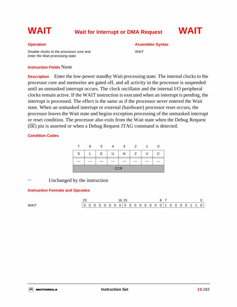
WAIT Wait for Interrupt or DMA Request WAIT
Instruction Fields None
Description Enter the low-power standby Wait processing state. The internal clocks to the processor core and memories are gated off, and all activity in the processor is suspended until an unmasked interrupt occurs. The clock oscillator and the internal I/O peripheral clocks remain active. If the WAIT instruction is executed when an interrupt is pending, the interrupt is processed. The effect is the same as if the processor never entered the Wait state. When an unmasked interrupt or external (hardware) processor reset occurs, the processor leaves the Wait state and begins exception processing of the unmasked interrupt or reset condition. The processor also exits from the Wait state when the Debug Request (DE) pin is asserted or when a Debug Request JTAG command is detected.
Condition Codes
Instruction Formats and Opcodes
Operation Assembler Syntax
Disable clocks to the processor core andenter the Wait processing state
WAIT
7 6 5 4 3 2 1 0
S L E U N Z V C
— — — — — — — —
CCR
— Unchanged by the instruction
23 16 15 8 7 0
WAIT 0 0 0 0 0 0 0 0 0 0 0 0 0 0 0 0 1 0 0 0 0 1 1 0
Instruction Set 13-183

13-184 DSP56300 Family Manual
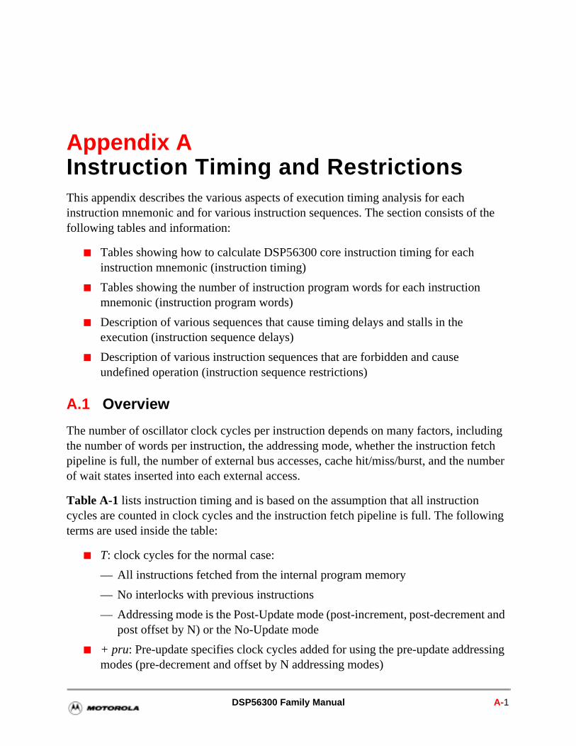
nt and
ssing
Appendix AInstruction Timing and RestrictionsThis appendix describes the various aspects of execution timing analysis for each instruction mnemonic and for various instruction sequences. The section consists of the following tables and information:
Tables showing how to calculate DSP56300 core instruction timing for each instruction mnemonic (instruction timing)
Tables showing the number of instruction program words for each instruction mnemonic (instruction program words)
Description of various sequences that cause timing delays and stalls in the execution (instruction sequence delays)
Description of various instruction sequences that are forbidden and cause undefined operation (instruction sequence restrictions)
A.1 Overview
The number of oscillator clock cycles per instruction depends on many factors, including the number of words per instruction, the addressing mode, whether the instruction fetch pipeline is full, the number of external bus accesses, cache hit/miss/burst, and the number of wait states inserted into each external access.
Table A-1 lists instruction timing and is based on the assumption that all instruction cycles are counted in clock cycles and the instruction fetch pipeline is full. The following terms are used inside the table:
T: clock cycles for the normal case:
— All instructions fetched from the internal program memory
— No interlocks with previous instructions
— Addressing mode is the Post-Update mode (post-increment, post-decremepost offset by N) or the No-Update mode
+ pru: Pre-update specifies clock cycles added for using the pre-update addremodes (pre-decrement and offset by N addressing modes)
DSP56300 Family Manual A-1
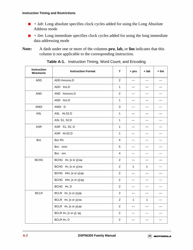
Instruction Timing and Restrictions
+ lab: Long absolute specifies clock cycles added for using the Long Absolute Address mode
+ lim: Long immediate specifies clock cycles added for using the long immediate data addressing mode
Note: A dash under one or more of the columns pru, lab, or lim indicates that this column is not applicable to the corresponding instruction.
Table A-1. Instruction Timing, Word Count, and Encoding
InstructionMnemonic
Instruction Format T + pru + lab + lim
ADD ADD #xxxxxx,D 2 — — —
ADD #xx,D 1 — — —
AND AND #xxxxxx,D 2 — — —
AND #xx,D 1 — — —
ANDI ANDI D 3 — — —
ASL ASL #ii,S2,D 1 — — —
ASL S1, S2,D 1 — — —
ASR ASR S1, S2, D 1 — — —
ASR #ii,S2,D 1 — — —
Bcc Bcc Rn 4 — — —
Bcc xxxx 5 — — —
Bcc xxx 4 — — —
BCHG BCHG #n, [x or y]:aa 2 — — —
BCHG #n, [x or y]:ea 2 1 1 —
BCHG ##n, [x or y]:pp 2 — — —
BCHG ##n, [x or y]:qq 2 — — —
BCHG #n, D 2 — — —
BCLR BCLR #n, [x or y]:pp 2 — — —
BCLR #n, [x or y]:ea 2 1 1 —
BCLR #n, [x or y]:aa 2 — — —
BCLR #n, [x or y]: qq 2 — — —
BCLR #n, D 2 — — —
A-2 DSP56300 Family Manual
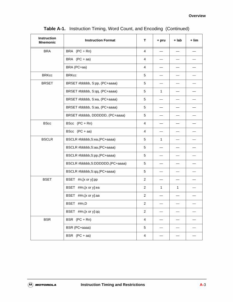
Overview
BRA BRA (PC + Rn) 4 — — —
BRA (PC + aa) 4 — — —
BRA (PC+aa) 4 — — —
BRKcc BRKcc 5 — — —
BRSET BRSET #bbbbb, S:pp, (PC+aaaa) 5 — — —
BRSET #bbbbb, S:qq, (PC+aaaa) 5 1 — —
BRSET #bbbbb, S:ea, (PC+aaaa) 5 — — —
BRSET #bbbbb, S:aa, (PC+aaaa) 5 — — —
BRSET #bbbbb, DDDDDD, (PC+aaaa) 5 — — —
BScc BScc (PC + Rn) 4 — — —
BScc (PC + aa) 4 — — —
BSCLR BSCLR #bbbbb,S:ea,(PC+aaaa) 5 1 — —
BSCLR #bbbbb,S:aa,(PC+aaaa) 5 — — —
BSCLR #bbbbb,S:pp,(PC+aaaa) 5 — — —
BSCLR #bbbbb,S:DDDDDD,(PC+aaaa) 5 — — —
BSCLR #bbbbb,S:qq,(PC+aaaa) 5 — — —
BSET BSET #n,[x or y]:pp 2 — — —
BSET ##n,[x or y]:ea 2 1 1 —
BSET ##n,[x or y]:aa 2 — — —
BSET ##n,D 2 — — —
BSET ##n,[x or y]:qq 2 — — —
BSR BSR (PC + Rn) 4 — — —
BSR (PC+aaaa) 5 — — —
BSR (PC + aa) 4 — — —
Table A-1. Instruction Timing, Word Count, and Encoding (Continued)
InstructionMnemonic
Instruction Format T + pru + lab + lim
Instruction Timing and Restrictions A-3
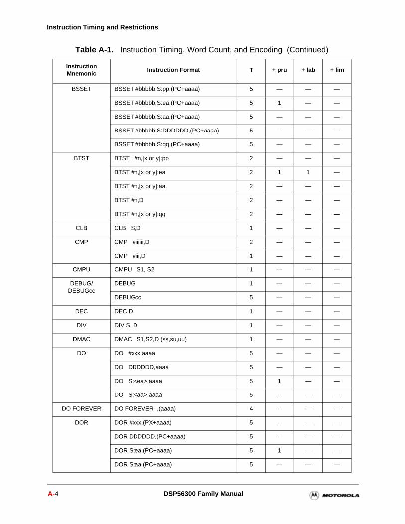
Instruction Timing and Restrictions
BSSET BSSET #bbbbb,S:pp,(PC+aaaa) 5 — — —
BSSET #bbbbb,S:ea,(PC+aaaa) 5 1 — —
BSSET #bbbbb,S:aa,(PC+aaaa) 5 — — —
BSSET #bbbbb,S:DDDDDD,(PC+aaaa) 5 — — —
BSSET #bbbbb,S:qq,(PC+aaaa) 5 — — —
BTST BTST #n,[x or y]:pp 2 — — —
BTST #n,[x or y]:ea 2 1 1 —
BTST #n,[x or y]:aa 2 — — —
BTST #n,D 2 — — —
BTST #n,[x or y]:qq 2 — — —
CLB CLB S,D 1 — — —
CMP CMP #iiiiii,D 2 — — —
CMP #iii,D 1 — — —
CMPU CMPU S1, S2 1 — — —
DEBUG/ DEBUGcc
DEBUG 1 — — —
DEBUGcc 5 — — —
DEC DEC D 1 — — —
DIV DIV S, D 1 — — —
DMAC DMAC S1,S2,D (ss,su,uu) 1 — — —
DO DO #xxx,aaaa 5 — — —
DO DDDDDD,aaaa 5 — — —
DO S:<ea>,aaaa 5 1 — —
DO S:<aa>,aaaa 5 — — —
DO FOREVER DO FOREVER ,(aaaa) 4 — — —
DOR DOR #xxx,(PX+aaaa) 5 — — —
DOR DDDDDD,(PC+aaaa) 5 — — —
DOR S:ea,(PC+aaaa) 5 1 — —
DOR S:aa,(PC+aaaa) 5 — — —
Table A-1. Instruction Timing, Word Count, and Encoding (Continued)
InstructionMnemonic
Instruction Format T + pru + lab + lim
A-4 DSP56300 Family Manual
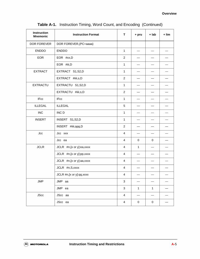
Overview
DOR FOREVER DOR FOREVER,(PC+aaaa)
ENDDO ENDDO 1 — — —
EOR EOR #xx,D 2 — — —
EOR #iii,D 1 — — —
EXTRACT EXTRACT S1,S2,D 1 — — —
EXTRACT #iiii,s,D 2 — — —
EXTRACTU EXTRACTU S1,S2,D 1 — — —
EXTRACTU #iiii,s,D 2 — — —
IFcc IFcc 1 — — —
ILLEGAL ILLEGAL 5 — — —
INC INC D 1 — — —
INSERT INSERT S1,S2,D 1 — — —
INSERT #iiii,qqq,D 2 — — —
Jcc Jcc xxx 4 — — —
Jcc ea 4 0 0 —
JCLR JCLR #n,[x or y]:ea,xxxx 4 1 — —
JCLR #n,[x or y]:pp,xxxx 4 — — —
JCLR #n,[x or y]:aa,xxxx 4 — — —
JCLR #n,S,xxxx 4 — — —
JCLR #n,[x or y]:qq,xxxx 4 — — —
JMP JMP aa 3 — — —
JMP ea 3 1 1 —
JScc JScc aa 4 — — —
JScc ea 4 0 0 —
Table A-1. Instruction Timing, Word Count, and Encoding (Continued)
InstructionMnemonic
Instruction Format T + pru + lab + lim
Instruction Timing and Restrictions A-5
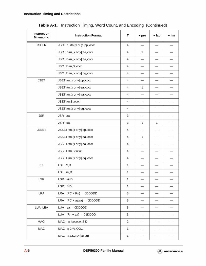
Instruction Timing and Restrictions
JSCLR JSCLR #n,[x or y]:pp,xxxx 4 — — —
JSCLR #n,[x or y]:ea,xxxx 4 1 — —
JSCLR #n,[x or y]:aa,xxxx 4 — — —
JSCLR #n,S,xxxx 4 — — —
JSCLR #n,[x or y]:qq,xxxx 4 — — —
JSET JSET #n,[x or y]:pp,xxxx 4 — — —
JSET #n,[x or y]:ea,xxxx 4 1 — —
JSET #n,[x or y]:aa,xxxx 4 — — —
JSET #n,S,xxxx 4 — — —
JSET #n,[x or y]:qq,xxxx 4 — — —
JSR JSR aa 3 — — —
JSR ea 3 1 1 —
JSSET JSSET #n,[x or y]:pp,xxxx 4 — — —
JSSET #n,[x or y]:ea,xxxx 4 1 — —
JSSET #n,[x or y]:aa,xxxx 4 — — —
JSSET #n,S,xxxx 4 — — —
JSSET #n,[x or y]:qq,xxxx 4 — — —
LSL LSL S,D 1 — — —
LSL #ii,D 1 — — —
LSR LSR #ii,D 1 — — —
LSR S,D 1 — — —
LRA LRA (PC + Rn) → 0DDDDD 3 — — —
LRA (PC + aaaa) → 0DDDDD 3 — — —
LUA, LEA LUA ea → 0DDDDD 3 — — —
LUA (Rn + aa) → 01DDDD 3 — — —
MACI MACI ± #xxxxxx,S,D 2 — — —
MAC MAC ± 2**s,QQ,d 1 — — —
MAC S1,S2,D (su,uu) 1 — — —
Table A-1. Instruction Timing, Word Count, and Encoding (Continued)
InstructionMnemonic
Instruction Format T + pru + lab + lim
A-6 DSP56300 Family Manual
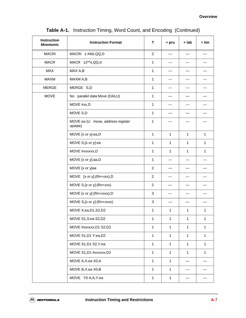
Overview
MACRI MACRI ± #iiiiii,QQ,D 2 — — —
MACR MACR ±2**s,QQ,d 1 — — —
MAX MAX A,B 1 — — —
MAXM MAXM A,B 1 — — —
MERGE MERGE S,D 1 — — —
MOVE No parallel data Move (DALU) 1 — — —
MOVE #xx,D 1 — — —
MOVE S,D 1 — — —
MOVE ea (U move, address register update)
1 — — —
MOVE [x or y]:ea,D 1 1 1 1
MOVE S,[x or y]:ea 1 1 1 1
MOVE #xxxxxx,D 1 1 1 1
MOVE [x or y]:aa,D 1 — — —
MOVE [x or y]aa 2 — — —
MOVE [x or y]:(Rn+xxx),D 2 — — —
MOVE S,[x or y]:(Rn+xxx) 2 — — —
MOVE [x or y]:(Rn+xxxx),D 3 — — —
MOVE S,[x or y]:(Rn+xxxx) 3 — — —
MOVE X:ea,D1,S2,D2 1 1 1 1
MOVE S1,S:ea S2,D2 1 1 1 1
MOVE #xxxxxx,D1 S2,D2 1 1 1 1
MOVE S1,D1 Y:ea,D2 1 1 1 1
MOVE S1,D1 S2,Y:ea 1 1 1 1
MOVE S1,D1 #xxxxxx,D2 1 1 1 1
MOVE A,X:ea X0,A 1 1 — —
MOVE B,X:ea X0,B 1 1 — —
MOVE Y0 A,A,Y:ea 1 1 — —
Table A-1. Instruction Timing, Word Count, and Encoding (Continued)
InstructionMnemonic
Instruction Format T + pru + lab + lim
Instruction Timing and Restrictions A-7
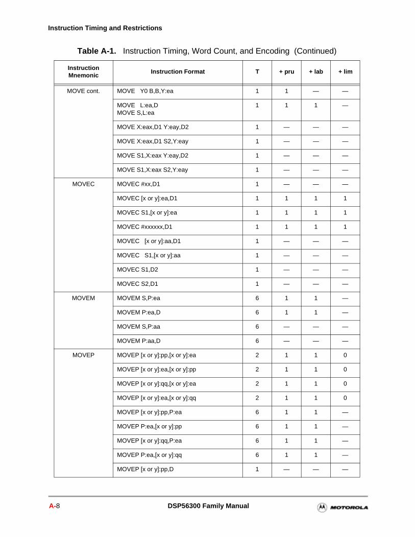
Instruction Timing and Restrictions
MOVE cont. MOVE Y0 B,B,Y:ea 1 1 — —
MOVE L:ea,DMOVE S,L:ea
1 1 1 —
MOVE X:eax,D1 Y:eay,D2 1 — — —
MOVE X:eax,D1 S2,Y:eay 1 — — —
MOVE S1,X:eax Y:eay,D2 1 — — —
MOVE S1,X:eax S2,Y:eay 1 — — —
MOVEC MOVEC #xx,D1 1 — — —
MOVEC [x or y]:ea,D1 1 1 1 1
MOVEC S1,[x or y]:ea 1 1 1 1
MOVEC #xxxxxx,D1 1 1 1 1
MOVEC [x or y]:aa,D1 1 — — —
MOVEC S1,[x or y]:aa 1 — — —
MOVEC S1,D2 1 — — —
MOVEC S2,D1 1 — — —
MOVEM MOVEM S,P:ea 6 1 1 —
MOVEM P:ea,D 6 1 1 —
MOVEM S,P:aa 6 — — —
MOVEM P:aa,D 6 — — —
MOVEP MOVEP [x or y]:pp,[x or y]:ea 2 1 1 0
MOVEP [x or y]:ea,[x or y]:pp 2 1 1 0
MOVEP [x or y]:qq,[x or y]:ea 2 1 1 0
MOVEP [x or y]:ea,[x or y]:qq 2 1 1 0
MOVEP [x or y]:pp,P:ea 6 1 1 —
MOVEP P:ea,[x or y]:pp 6 1 1 —
MOVEP [x or y]:qq,P:ea 6 1 1 —
MOVEP P:ea,[x or y]:qq 6 1 1 —
MOVEP [x or y]:pp,D 1 — — —
Table A-1. Instruction Timing, Word Count, and Encoding (Continued)
InstructionMnemonic
Instruction Format T + pru + lab + lim
A-8 DSP56300 Family Manual
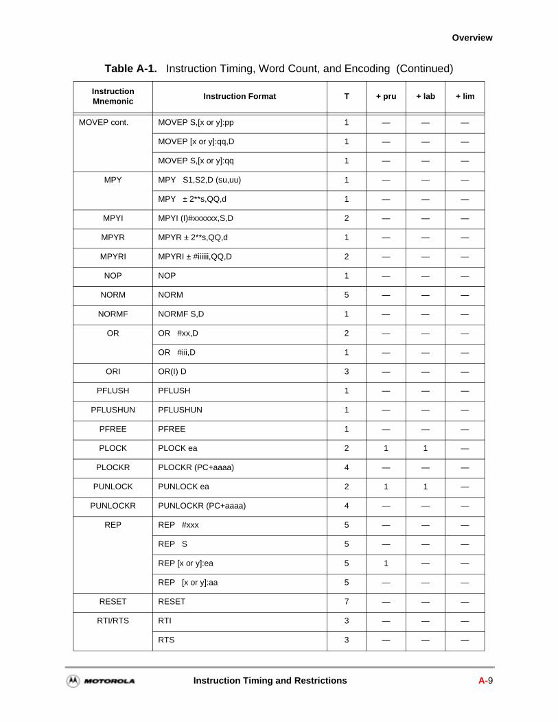
Overview
MOVEP cont. MOVEP S,[x or y]:pp 1 — — —
MOVEP [x or y]:qq,D 1 — — —
MOVEP S,[x or y]:qq 1 — — —
MPY MPY S1,S2,D (su,uu) 1 — — —
MPY ± 2**s,QQ,d 1 — — —
MPYI MPYI (I)#xxxxxx,S,D 2 — — —
MPYR MPYR ± 2**s,QQ,d 1 — — —
MPYRI MPYRI ± #iiiiii,QQ,D 2 — — —
NOP NOP 1 — — —
NORM NORM 5 — — —
NORMF NORMF S,D 1 — — —
OR OR #xx,D 2 — — —
OR #iii,D 1 — — —
ORI OR(I) D 3 — — —
PFLUSH PFLUSH 1 — — —
PFLUSHUN PFLUSHUN 1 — — —
PFREE PFREE 1 — — —
PLOCK PLOCK ea 2 1 1 —
PLOCKR PLOCKR (PC+aaaa) 4 — — —
PUNLOCK PUNLOCK ea 2 1 1 —
PUNLOCKR PUNLOCKR (PC+aaaa) 4 — — —
REP REP #xxx 5 — — —
REP S 5 — — —
REP [x or y]:ea 5 1 — —
REP [x or y]:aa 5 — — —
RESET RESET 7 — — —
RTI/RTS RTI 3 — — —
RTS 3 — — —
Table A-1. Instruction Timing, Word Count, and Encoding (Continued)
InstructionMnemonic
Instruction Format T + pru + lab + lim
Instruction Timing and Restrictions A-9
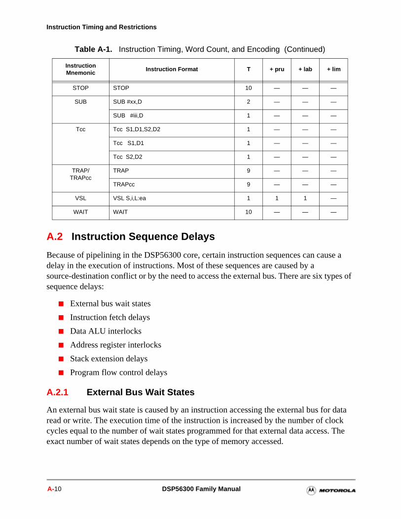
Instruction Timing and Restrictions
A.2 Instruction Sequence Delays
Because of pipelining in the DSP56300 core, certain instruction sequences can cause a delay in the execution of instructions. Most of these sequences are caused by a source-destination conflict or by the need to access the external bus. There are six types of sequence delays:
External bus wait states
Instruction fetch delays
Data ALU interlocks
Address register interlocks
Stack extension delays
Program flow control delays
A.2.1 External Bus Wait States
An external bus wait state is caused by an instruction accessing the external bus for data read or write. The execution time of the instruction is increased by the number of clock cycles equal to the number of wait states programmed for that external data access. The exact number of wait states depends on the type of memory accessed.
STOP STOP 10 — — —
SUB SUB #xx,D 2 — — —
SUB #iii,D 1 — — —
Tcc Tcc S1,D1,S2,D2 1 — — —
Tcc S1,D1 1 — — —
Tcc S2,D2 1 — — —
TRAP/TRAPcc
TRAP 9 — — —
TRAPcc 9 — — —
VSL VSL S,i,L:ea 1 1 1 —
WAIT WAIT 10 — — —
Table A-1. Instruction Timing, Word Count, and Encoding (Continued)
InstructionMnemonic
Instruction Format T + pru + lab + lim
A-10 DSP56300 Family Manual
Instruction Sequence Delays
ond
n.
A.2.2 Instruction Fetch Delays
At an external instruction fetch, the effective number of stall states in the pipeline is the number specified in the Bus Control Register (BCR).
A.2.3 Data ALU Interlock
A Data ALU interlock is caused by one of the following sequences:
Arithmetic stall: Occurs when an instruction uses one of the Data ALU registers (A0, A1, A2, B0, B1, or B2) or accumulators (A or B) as a source register for the move portion of the instruction when the preceding instruction is an arithmetic instruction1 that uses the same accumulator as its destination. Delays execution of the initiating instruction by one clock cycle.
Transfer stall: Occurs when an instruction uses one of the Data ALU registers (A0, A1, A2, B0, B1, or B2) or accumulators (A or B) as a source register for the move portion of the instruction when the preceding instruction uses the corresponding accumulator or one of the Data ALU registers that comprise the accumulator as its destination register in the move portion of that instruction. Delays execution of the initiating instruction by one instruction cycle.
Status stall: Occurs when an instruction reads the contents of the Status Register (SR) for either a move operation or bit testing and the preceding or the second preceding instruction is an arithmetic instruction. Delays execution of the initiating instruction by two instruction cycles for a move operation or one instruction cycle for bit testing.
A.2.4 Address Register Interlocks
An address register interlock is caused by one of the following sequences:
Conditional Transfer Interlock: Occurs when a Transfer On-Condition (Tcc) instruction is followed by an instruction that explicitly specifies one of the address generation registers (R[0–7]) as its source operand. Delays execution of the secinstruction by one instruction cycle.
Address Generation Interlock: Occurs when the move portion of an instruction uses one of the AGU registers (R[0–7]) for address generation or for addresscalculation, while one of the three preceding instruction cycles uses one of theregister set (Ri, Ni or Mi) members as a destination register in its move portioConsider Example A-1.
1. An arithmetic instruction uses the internal Data ALU data paths.
Instruction Timing and Restrictions A-11
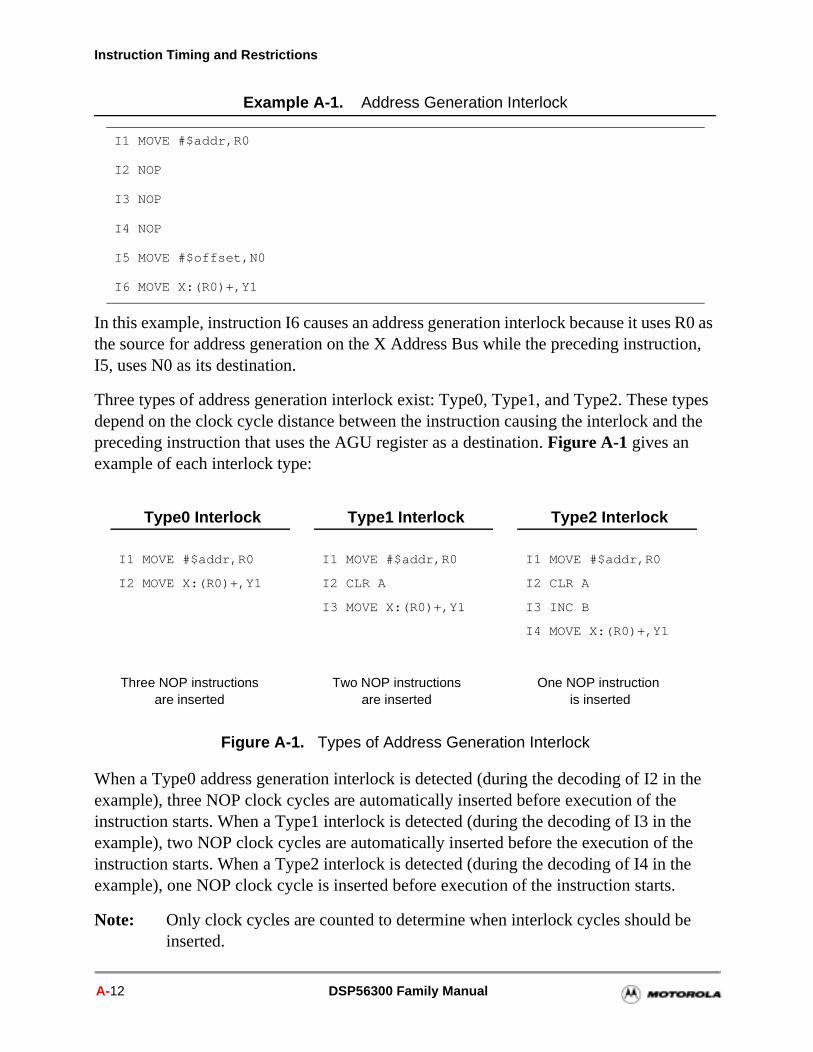
Instruction Timing and Restrictions
In this example, instruction I6 causes an address generation interlock because it uses R0 as the source for address generation on the X Address Bus while the preceding instruction, I5, uses N0 as its destination.
Three types of address generation interlock exist: Type0, Type1, and Type2. These types depend on the clock cycle distance between the instruction causing the interlock and the preceding instruction that uses the AGU register as a destination. Figure A-1 gives an example of each interlock type:
When a Type0 address generation interlock is detected (during the decoding of I2 in the example), three NOP clock cycles are automatically inserted before execution of the instruction starts. When a Type1 interlock is detected (during the decoding of I3 in the example), two NOP clock cycles are automatically inserted before the execution of the instruction starts. When a Type2 interlock is detected (during the decoding of I4 in the example), one NOP clock cycle is inserted before execution of the instruction starts.
Note: Only clock cycles are counted to determine when interlock cycles should be inserted.
Example A-1. Address Generation Interlock
I1 MOVE #$addr,R0
I2 NOP
I3 NOP
I4 NOP
I5 MOVE #$offset,N0
I6 MOVE X:(R0)+,Y1
Figure A-1. Types of Address Generation Interlock
Type0 Interlock
I1 MOVE #$addr,R0
I2 MOVE X:(R0)+,Y1
Type1 Interlock
I1 MOVE #$addr,R0
I2 CLR A
I3 MOVE X:(R0)+,Y1
Type2 Interlock
I1 MOVE #$addr,R0
I2 CLR A
I3 INC B
I4 MOVE X:(R0)+,Y1
Three NOP instructionsare inserted
Two NOP instructionsare inserted
One NOP instruction is inserted
A-12 DSP56300 Family Manual
Instruction Sequence Delays
When an instruction using one of the AGU registers as an address generation enters the decoding stage of the DSP56300 core, the distance from that instruction to the preceding instruction using the register as destination is measured in clock cycles to determine the existence and type of address generation interlock. Once an address generation interlock is detected, the appropriate number of NOP clock cycles is inserted. The following instructions take these additional cycles into account for detecting a possible new address generation interlock. Example A-2 demonstrates this feature.
In this example, a Type1 interlock is detected during the decoding phase of I 3 and two NOP cycles are inserted before that instruction executes. During the decoding of I4, no address generation interlock is detected, so no NOP cycles are inserted. However, if I3 were an instruction that did not use R0, a Type2 address generation interlock would be detected during the decoding phase of I4, and one NOP cycle would be inserted before the instruction executes.
A.2.5 Stack Extension Delays
Some instructions access the System Stack (SS) as part of their normal activity. When the SS is either completely full or empty, the special stack extension mechanism is engaged and the access completes only after an access to data memory is automatically performed. This delays the decoding and the execution phases of that instruction. A stack-full or a stack-empty state is defined by the contents of the Stack Counter (SC) register. When the stack counter equals 14, the on-chip hardware stack contains fourteen words (a stack word is a 48-bit long word combined from the low and the high portions of the stack). The stack is declared as stack-full, and any additional push operation activates the stack extension mechanism. When the stack counter equals 2, the on-chip hardware stack contains only two words. The stack is declared as stack-empty, and any additional pop operations activate the stack extension mechanism. The instructions/cases listed in Table A-2 cause an access to the system stack and may engage the stack extension mechanism.
Example A-2. Detection of Address Generation Interlock
I1 MOVE #$addr,R0
I2 CLR A
I3 MOVE X:(R0)+,Y1
I4 MOVE X:(R0)+,Y0
Instruction Timing and Restrictions A-13
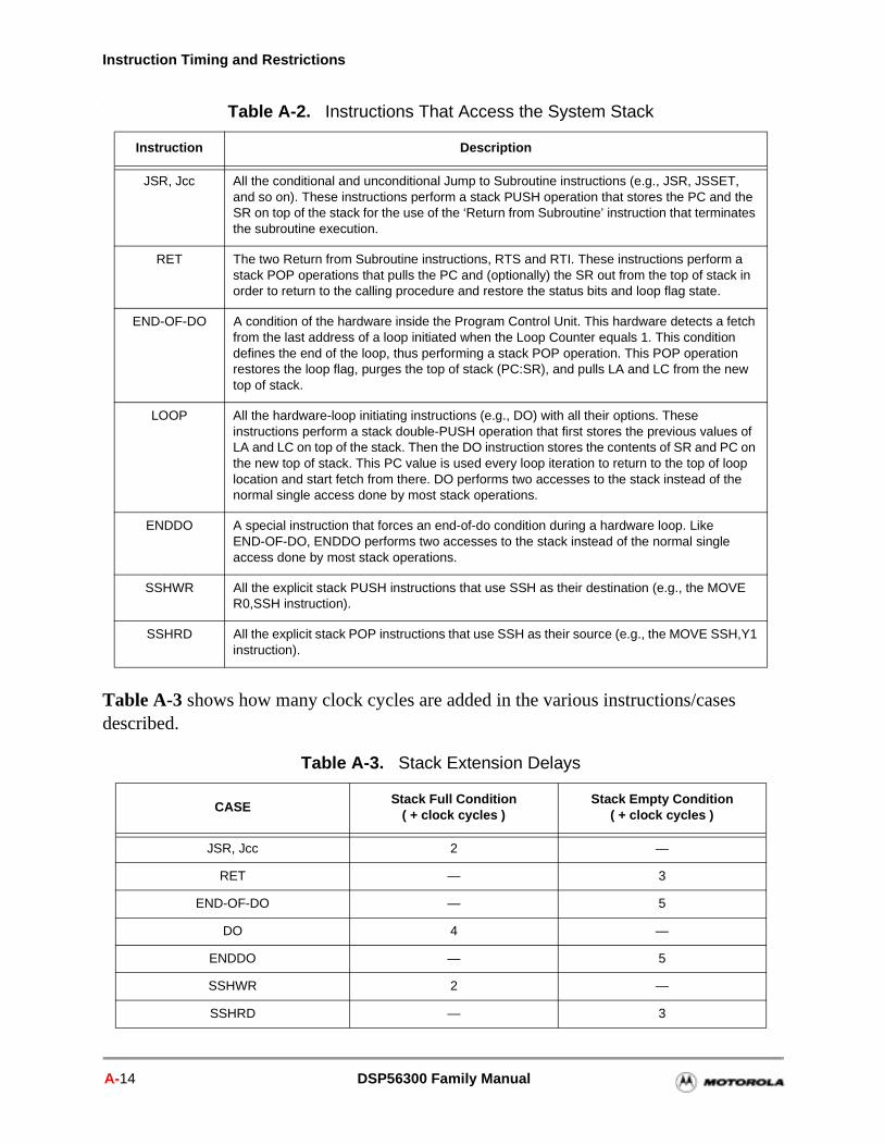
Instruction Timing and Restrictions
:
Table A-3 shows how many clock cycles are added in the various instructions/cases described.
:
Table A-2. Instructions That Access the System Stack
Instruction Description
JSR, Jcc All the conditional and unconditional Jump to Subroutine instructions (e.g., JSR, JSSET, and so on). These instructions perform a stack PUSH operation that stores the PC and the SR on top of the stack for the use of the ‘Return from Subroutine’ instruction that terminates the subroutine execution.
RET The two Return from Subroutine instructions, RTS and RTI. These instructions perform a stack POP operations that pulls the PC and (optionally) the SR out from the top of stack in order to return to the calling procedure and restore the status bits and loop flag state.
END-OF-DO A condition of the hardware inside the Program Control Unit. This hardware detects a fetch from the last address of a loop initiated when the Loop Counter equals 1. This condition defines the end of the loop, thus performing a stack POP operation. This POP operation restores the loop flag, purges the top of stack (PC:SR), and pulls LA and LC from the new top of stack.
LOOP All the hardware-loop initiating instructions (e.g., DO) with all their options. These instructions perform a stack double-PUSH operation that first stores the previous values of LA and LC on top of the stack. Then the DO instruction stores the contents of SR and PC on the new top of stack. This PC value is used every loop iteration to return to the top of loop location and start fetch from there. DO performs two accesses to the stack instead of the normal single access done by most stack operations.
ENDDO A special instruction that forces an end-of-do condition during a hardware loop. Like END-OF-DO, ENDDO performs two accesses to the stack instead of the normal single access done by most stack operations.
SSHWR All the explicit stack PUSH instructions that use SSH as their destination (e.g., the MOVE R0,SSH instruction).
SSHRD All the explicit stack POP instructions that use SSH as their source (e.g., the MOVE SSH,Y1 instruction).
Table A-3. Stack Extension Delays
CASEStack Full Condition
( + clock cycles )Stack Empty Condition
( + clock cycles )
JSR, Jcc 2 —
RET — 3
END-OF-DO — 5
DO 4 —
ENDDO — 5
SSHWR 2 —
SSHRD — 3
A-14 DSP56300 Family Manual

Instruction Sequence Delays
nd
ction
n
A.2.6 Program Flow Control Delays
When flow-control instructions execute, some boundary cases exist and introduce pipeline interlocks into the program flow. These interlocks lengthen the decoding phase of the instructions, thus delaying execution. The following sequences represent unusual operations that will probably never be used. The detection of these cases and the generation of interlocks is done to maintain object code compatibility between the DSP56300 core and the 56000 family of DSPs. The following terms are used in this discussion:
I1: An address of an instruction, where I2, I3, and I4 indicate the next instructions in the program flow
MOVE: any type of MOVE, MOVEM, MOVEP, MOVEC, BSET, BCHG, BCLR, and BTST
LA: the last address of a DO LOOP
(LA – 1): the address of an instruction word located at LA – 1
CR: Control Register, every one of the registers LA, LC, SR, SP, SSH, SSL, aOMR
A.2.6.1 JMP to LA or to LA – 1
When I1 is any type of JMP with its target address equal to LA, the decoding phase of the instruction following the instruction at LA is delayed by 2 clock cycles. When I1 is any type of JMP with its target address equal to LA – 1, the decoding phase of the instrufollowing the instruction at LA is delayed by one clock cycle.
A.2.6.2 RTI to LA or to LA – 1
When I1 is an RTI instruction whose return address is LA, the decoding phase of the instruction following the instruction at LA is delayed by two clock cycles. When I1 is an RTI instruction whose return address is LA – 1, the decoding phase of the instructiofollowing the instruction at LA is delayed by one clock cycle.
A.2.6.3 Conditional Instructions
When I1 is a conditional change of flow instruction (such as Jcc) and the condition isfalse, the decoding phase of I2 is delayed by one clock cycle.
Instruction Timing and Restrictions A-15
Instruction Timing and Restrictions
into
of I1
uction
n st of tack e used
d as
d a
ne of
A.2.6.4 Interrupt Abort
When I1 is an instruction with a decoding phase that is longer than one cycle, it may be aborted by the Interrupt Control Unit. In this case, a one clock cycle “hole” is insertedthe pipeline, after which the instruction at the interrupt vector is decoded.
A.2.6.5 Degenerated DO loop
When I1 is a DO loop but the loop contains only one instruction, the decoding phaseis lengthened by one clock cycle.
A.2.6.6 Annulled REP and DO
If the repeat count of a REP instruction is zero, the decoding phase of the REP instris lengthened by one clock cycle. If the repeat count of a DO instruction is zero, the decoding phase of the DO instruction is lengthened by three clock cycles.
A.3 Instruction Sequence Restrictions
Because of the pipelining in the DSP56300 core central processor, certain instructiosequences are forbidden. Use of these sequences causes undefined operation. Mothese restricted sequences cause contention for an internal resource, such as the SRegister. The DSP Assembler flags these as assembly errors. The following terms arin this discussion:
MOVE: any type of MOVE, MOVEM, MOVEP, MOVEC
MOVEM: any type of MOVE to/from the Program space
LA: the last address of a DO LOOP
Two-words <inst>: a double-word instruction in which the second word is usean immediate data or absolute address
Single-word <inst>: an instruction with an addressing mode that does not neesecond word extension
A.3.1 Restrictions Near the End of DO Loops
Proper DO loop operation is not guaranteed for an instruction sequence similar to othe following sequences.
A-16 DSP56300 Family Manual
Instruction Sequence Restrictions
At LA – 5: The following instructions should not start at address LA – 5:
— Single-word or two-word MOVE to LA, LC, SP, SC, SSH, SSL, SZ, VBA, OMR
— BCHG, BSET, BCLR on LA, LC, SP, SC, SSH, SSL, SZ, VBA, OMR
At LA – 4: The following instructions should not start at address LA – 4:
— Single-word or two-word MOVE to LA, LC, SP, SC, SSH, SSL, SZ, VBA, OMR
— BCHG, BSET, BCLR on LA, LC, SP, SC, SSH, SSL, SZ, VBA, OMR
At LA – 3: The following instructions should not start at address LA – 3:
— BCHG, BSET, BCLR on LA, LC, SP, SC, SSH, SSL, SZ, VBA, OMR
— MOVE to LA, LC, SP, SC, SSH, SSL, SZ, VBA, OMR
— MOVE from SSH, SSL
— Two-word JMP, Jcc, JSR, JScc
— JSET, JCLR, JSSET, JSCLR
— Two-word MOVEM
At LA – 2: The following instructions should not start at address LA – 2:
— DO, DOR, DO FOREVER
— MOVE to/from LA, LC, SP,SC, SSH, SSL,SZ, VBA, OMR
— BCHG, BSET, BCLR, BTST on LA, LC, SP, SC, SSH, SSL, SZ, VBA, OMR
— JMP, Jcc, JSR, JScc, JSET, JCLR, JSSET, JSCLR, BRA, Bcc, BSR, BScc
— MOVEM
— ANDI, ORI on MR
— BRKcc, ENDDO, REP
— STOP, WAIT, DEBUG, DEBUGcc, TRAP, TRAPcc, ILLEGAL
At LA – 1: The following instructions should not start at address LA – 1:
— DO, DOR, DO FOREVER
— MOVE to/from LA, LC, SP, SC, SSH, SSL, SZ, VBA, OMR
— BCHG, BSET, BCLR, BTST on LA, LC, SP, SC, SSH, SSL, SZ, VBA, OMR
— JMP, Jcc, JSR, JScc, JSET, JCLR, JSSET, JSCLR, BRA, Bcc, BSR, BScc
— MOVEM
Instruction Timing and Restrictions A-17
Instruction Timing and Restrictions
e
s).
— ANDI, ORI on MR
— BRKcc, ENDDO, REP
— STOP, WAIT, DEBUG, DEBUGcc, TRAP, TRAPcc, ILLEGAL
Note: A one-word conditional branch instruction at LA-1 is not allowed.
When two consecutive LAs have a conditional branch instruction at LA-1 of thinternal loop, the device does not operate properly. For example, the followingsequence may generate incorrect results:
DO #5, LABEL1NOPDO #4, LABEL2NOP MOVE (R0) +BSCC _DEST ; conditional branch at LA-1 of internal loopNOP ; internal LA
LABEL2NOP ; external LA
LABEL1NOP NOP
_DEST NOPNOP RTS
Workaround: Put an additional NOP between LABEL2 and LABEL1.
At LA: The following instructions should not start at address LA:
— Any two-word instruction
— MOVE to LA, LC, SP, SC, SSH, SSL, SZ, VBA, OMR
— MOVE from SSH, SSL
— BCHG, BSET, BCLR on LA, LC, SP, SC, SSH, SSL, SZ, VBA, OMR
— BTST on SSH
— JMP, JSR, BRA, BSR, Jcc, JScc, Bcc, BScc
— MOVE to/from Program space MOVEM, MOVEP (only the P space option
— RESET
— RTI, RTS
— ANDI, ORI on MR
— BRKcc, ENDDO, REP
— STOP, WAIT, DEBUG, DEBUGcc, TRAP, TRAPcc, ILLEGAL
A-18 DSP56300 Family Manual
Instruction Sequence Restrictions
a DO
,
R,
nside sted e wing VER
A.3.2 General DO Restrictions
The general restrictions on DO instructions are as follows:
A DO loop should be initialized and aborted using only the following instructions: DO, DOR, DO FOREVER, ENDDO, and BRKcc.
The LF and the FV bits in the Status Register (SR) should not be explicitly changed using the MOVE, BCHG, BSET, BCLR, ANDI, or ORI instructions.
Proper DO loop operation is not guaranteed if an instruction sequence similar to one of the following sequences is used.
— SSH cannot be used as the source for the Loop-Count for a DO, DOR, or FOREVER instruction.
— The following instructions should not appear within four words before a DODOR, or DO FOREVER:
• BCHG, BCLR, BSET, MOVE on/to SSH,SSL
• BCHG, BCLR, BSET, MOVE on/to SP, SC
— The following instructions should not appear immediately before a DO, DOor DO FOREVER:
• MOVE from SSH
• BTST on SSH
• BCHG, BCLR, BSET, MOVE to/on LA, LC, SP, SC, SSH, SSL
• JSR, JScc, JSSET, JSCLR to LA whenever LF is set
• BSR, BScc, to LA whenever LF is set
When Stack Extension mode is enabled, use of the BRKcc or ENDDO instructions iDO loops may cause an improper operation. If the loop is not nested and has no neloop inside it, this restriction is relevant only if LA or LC values are in use outside thloop. If Stack Extension is used, emulate the BRKcc or ENDDO as shown in the folloexamples in which there is a split between two cases, finite DO loops and DO FOREloops.
Instruction Timing and Restrictions A-19
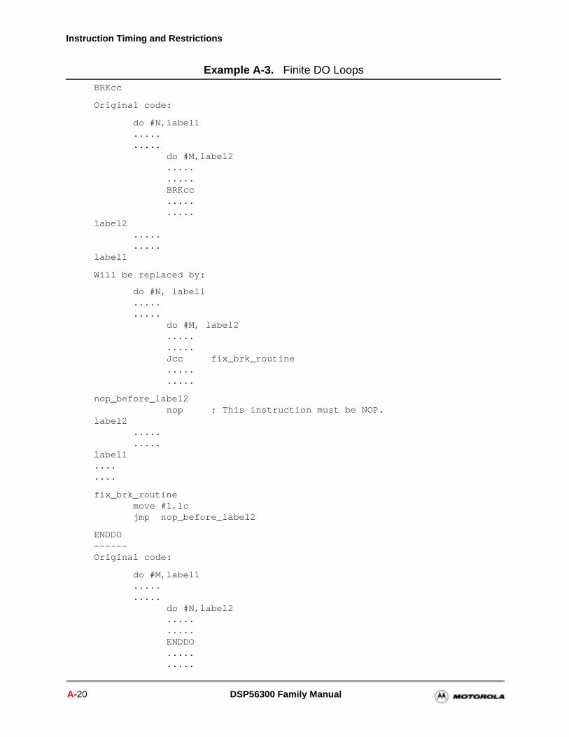
Instruction Timing and Restrictions
Example A-3. Finite DO Loops
BRKcc
Original code:
do #N,label1..........
do #M,label2..........BRKcc..........
label2..........
label1
Will be replaced by:
do #N, label1..........
do #M, label2..........Jcc fix_brk_routine..........
nop_before_label2nop ; This instruction must be NOP.
label2..........
label1........
fix_brk_routinemove #1,lcjmp nop_before_label2
ENDDO------Original code:
do #M,label1..........
do #N,label2..........ENDDO..........
A-20 DSP56300 Family Manual
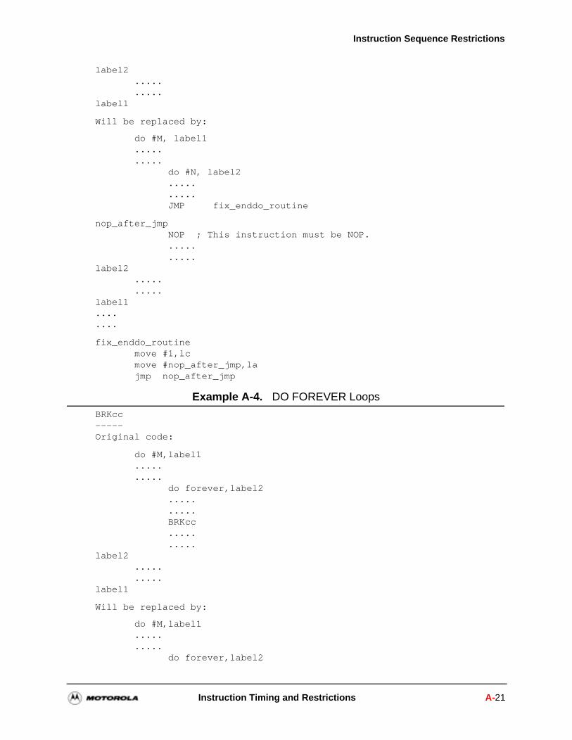
Instruction Sequence Restrictions
label2..........
label1
Will be replaced by:
do #M, label1..........
do #N, label2..........JMP fix_enddo_routine
nop_after_jmpNOP ; This instruction must be NOP...........
label2..........
label1........
fix_enddo_routinemove #1,lcmove #nop_after_jmp,lajmp nop_after_jmp
Example A-4. DO FOREVER Loops
BRKcc-----Original code:
do #M,label1..........
do forever,label2..........BRKcc..........
label2..........
label1
Will be replaced by:
do #M,label1..........
do forever,label2
Instruction Timing and Restrictions A-21
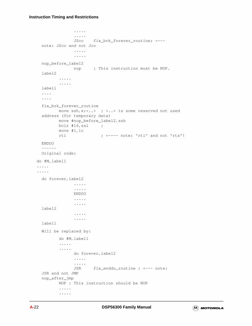
Instruction Timing and Restrictions
.....
.....JScc fix_brk_forever_routine; <---
note: JScc and not Jcc..........
nop_before_label2nop ; This instruction must be NOP.
label2..........
label1........
fix_brk_forever_routinemove ssh,x:<..> ; <..> is some reserved not used
address (for temporary data)move #nop_before_label2,sshbclr #16,ssl ;move #1,lcrti ; <---- note: "rti" and not "rts"!
ENDDO------Original code:
do #M,label1..........
do forever,label2..........ENDDO..........
label2..........
label1
Will be replaced by:
do #M,label1..........
do forever,label2..........JSR fix_enddo_routine ; <--- note:
JSR and not JMPnop_after_jmp
NOP ; This instruction should be NOP..........
A-22 DSP56300 Family Manual
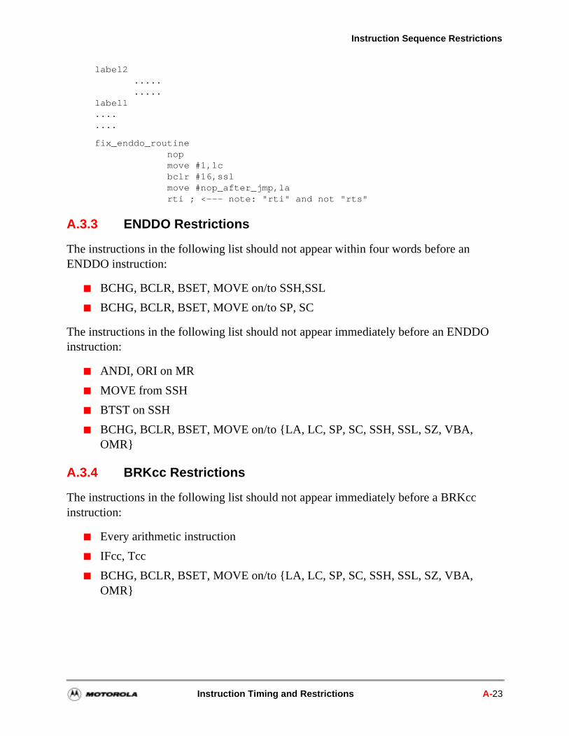
Instruction Sequence Restrictions
label2..........
label1........
fix_enddo_routinenopmove #1,lcbclr #16,sslmove #nop_after_jmp,larti ; <--- note: "rti" and not "rts"
A.3.3 ENDDO Restrictions
The instructions in the following list should not appear within four words before an ENDDO instruction:
BCHG, BCLR, BSET, MOVE on/to SSH,SSL
BCHG, BCLR, BSET, MOVE on/to SP, SC
The instructions in the following list should not appear immediately before an ENDDO instruction:
ANDI, ORI on MR
MOVE from SSH
BTST on SSH
BCHG, BCLR, BSET, MOVE on/to LA, LC, SP, SC, SSH, SSL, SZ, VBA, OMR
A.3.4 BRKcc Restrictions
The instructions in the following list should not appear immediately before a BRKcc instruction:
Every arithmetic instruction
IFcc, Tcc
BCHG, BCLR, BSET, MOVE on/to LA, LC, SP, SC, SSH, SSL, SZ, VBA, OMR
Instruction Timing and Restrictions A-23
Instruction Timing and Restrictions
A.3.5 RTI and RTS Restrictions
The instructions in the following list should not appear immediately before an RTI instruction:
MOVE, BCHG, BCLR, BSET on SSH, SSL, SP, SC
MOVE, BTST from/on SSH
ANDI, ORI on MR, CCR
ENDDO
The instructions in the following list should not appear immediately before an RTS instruction:
MOVE, BCHG, BCLR, BSET on SSH, SSL, SP, SC
MOVE, BTST from/on SSH
ENDDO
A.3.6 SP/SC and SSH/SSL Manipulation Restrictions
The instructions in List A should not be executed within four instructions before executing any of the instructions in List B.
List A
MOVE to (SP, SC)
BCHG, BSET, BCLR on (SP, SC)
List B
MOVE to/from SSH,SSL
BTST, BCHG, BSET, BCLR on SSH,SSL
JSET, JCLR, JSSET, JSCLR on SSH,SSL
A-24 DSP56300 Family Manual
Instruction Sequence Restrictions
A.3.7 Fast Interrupt Routines
The following instructions cannot be used in a fast interrupt routine:
DO, DO FOREVER, REP
ENDDO, BRKcc
RTI, RTS
STOP, WAIT
TRAP, TRAPcc
ANDI, ORI on MR, CCR
MOVE from SSH
BTST on SSH
MOVE to LA, LC, SP, SC, SSH, SSL
BCHG, BSET, BCLR on LA, LC, SP, SC, SSH, SSL
A.3.8 REP Restrictions
The REP instruction can repeat any single-word instruction except the REP instruction itself and any instruction that changes program flow. The following instructions are not allowed to follow a REP instruction (cannot be repeated):
REP, DO, DO FOREVER
ENDDO, BRKcc
JMP, Jcc, JCLR, JSET
JSR, JScc, JSCLR, JSSET
BRA, Bcc
BSR, BScc
RTS, RTI
TRAP, TRAPcc
WAIT, STOP
When an instruction with all the following conditions follows a repeat instruction, then the last move will be corrupted:
The repeated instruction is from external memory.
The repeated instruction is a DALU instruction that includes two DALU registers, one as a source, and one as destination (for example, tfr, add).
Instruction Timing and Restrictions A-25
Instruction Timing and Restrictions
The repeated instruction has a double move in parallel to the DALU instruction: one move’s source is the destination of the DALU instruction (causing a DALU interlock); the other move’s destination is the source of the DALU instruction.
Example:
In this example, the second iteration before the last, the "x(r0)+,x0" does not happen. On the first iteration before the last, the X0 register is fixed with the "x(r0)+,x0", but the "tfr x0,a" gets the wrong value from the previous iteration’s X0. Thus, at the last iteration the A register is fixed with "tfr x0,a", but the "a,y0" transfers the wrong value from the previous iteration’s A register to Y0.
Workaround:
1. Use the DO instruction instead; mask any necessary interrupts before the DO.
2. Run the REP instructions from internal memory.
3. Do not make DALU interlocks in the repeated instruction. After the repeat make the move. In the example above, all the "move a,y0" are redundant so it can be done in the next instruction:
rep #numbertfr x0,a x:(r0)+,x0 move a,y0
If you must have no interrupts before the move, mask the interrupts before the REP instruction.
A.3.9 Stack Extension Restrictions
The following instructions, related to the operation of the on-chip hardware stack extension, cannot be used whenever the stack extension is enabled:
MOVE to EP
BCHG, BSET, BCLR on EP
MOVE to SC with a value greater than 15
rep #number
tfr x0,a x:(r0)+,x0 a,y0 ;This instruction is from external memory
This is condition 3, second part
This is condition 3, first part-DALU interlock
A-26 DSP56300 Family Manual
Peripheral Pipeline Restrictions
SH
SH
lt SL T,
esult SL T,
n.
tively lines ge of
The following instructions, related to the operation of the on-chip hardware stack extension, cannot be placed in the stack error vector locations whenever the stack extension is enabled:
JSR, JScc, JSCLR, JSSET
BSR, BScc
A.3.10 Stack Extension Enable Restrictions
When stack extension is enabled, the read result from stack may be improper if two previous executed instructions cause sequential read and write operations with SSH. Two cases are possible:
Case 1:
— For the first executed instruction: move from SSH or bit manipulation on S(that is, JCLR, BRCLR, JSET, BRSET, BTST, BSSET, JSSET, BSCLR, JSCLR).
— For the second executed instruction: move to SSH or bit manipulation on S(that is, JSR, BSR, JScc, BScc).
— For the third executed instruction: an SSL or SSH read from the stack resumay be improper. Move from SSH or SSL or bit manipulation on SSH or S(that is, BSET, BCLR, BCHG, JCLR, BRCLR, JSET, BRSET, BTST, BSSEJSSET, BSCLR, JSCLR).
Workaround: Add two NOP instructions before the third executed instruction.
Case 2:
— For the first executed instruction: bit manipulation on SSH (that is, BSET, BCLR, BCJG).
— For the second executed instruction: an SSL or SSH read from the stack rmay be improper. Move from SSH or SSL or bit manipulation on SSH or S(that is, BSET, BCLR, BCHG, JCLR, BRCLR, JSET, BRSET, BTST, BSSEJSSET, BSCLR, JSCLR).
Workaround: Add two NOP instructions before the second executed instructio
A.4 Peripheral Pipeline Restrictions
The DSP56300 core is based on a highly optimized pipeline engine. Despite the reladeep pipeline (seven stages), the latency effects normally associated with long pipeare minimal because most of these effects are transparent to the user. Such designtechniques as forwarding and interlocking alleviate the need for a thorough knowled
Instruction Timing and Restrictions A-27
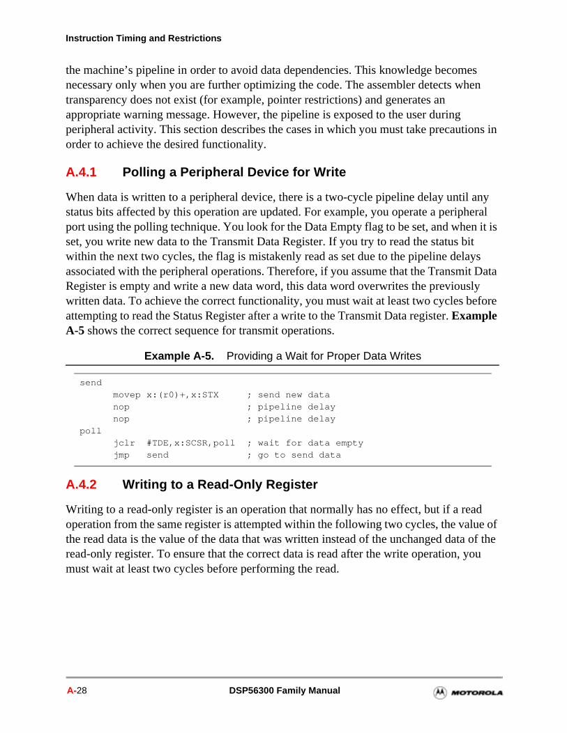
Instruction Timing and Restrictions
es en
ons in
any heral it is
it ys it Data ly efore
d ue of of the ou
the machine’s pipeline in order to avoid data dependencies. This knowledge becomnecessary only when you are further optimizing the code. The assembler detects whtransparency does not exist (for example, pointer restrictions) and generates an appropriate warning message. However, the pipeline is exposed to the user during peripheral activity. This section describes the cases in which you must take precautiorder to achieve the desired functionality.
A.4.1 Polling a Peripheral Device for Write
When data is written to a peripheral device, there is a two-cycle pipeline delay until status bits affected by this operation are updated. For example, you operate a peripport using the polling technique. You look for the Data Empty flag to be set, and whenset, you write new data to the Transmit Data Register. If you try to read the status bwithin the next two cycles, the flag is mistakenly read as set due to the pipeline delaassociated with the peripheral operations. Therefore, if you assume that the TransmRegister is empty and write a new data word, this data word overwrites the previouswritten data. To achieve the correct functionality, you must wait at least two cycles battempting to read the Status Register after a write to the Transmit Data register. Example A-5 shows the correct sequence for transmit operations.
A.4.2 Writing to a Read-Only Register
Writing to a read-only register is an operation that normally has no effect, but if a reaoperation from the same register is attempted within the following two cycles, the valthe read data is the value of the data that was written instead of the unchanged dataread-only register. To ensure that the correct data is read after the write operation, ymust wait at least two cycles before performing the read.
Example A-5. Providing a Wait for Proper Data Writes
sendmovep x:(r0)+,x:STX ; send new datanop ; pipeline delaynop ; pipeline delay
polljclr #TDE,x:SCSR,poll ; wait for data emptyjmp send ; go to send data
A-28 DSP56300 Family Manual
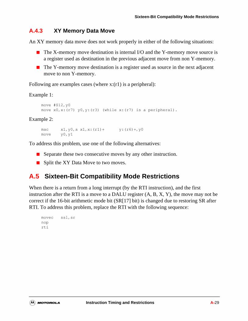
Sixteen-Bit Compatibility Mode Restrictions
A.4.3 XY Memory Data Move
An XY memory data move does not work properly in either of the following situations:
The X-memory move destination is internal I/O and the Y-memory move source is a register used as destination in the previous adjacent move from non Y-memory.
The Y-memory move destination is a register used as source in the next adjacent move to non Y-memory.
Following are examples cases (where x:(r1) is a peripheral):
Example 1:
move #$12,y0 move x0,x:(r7) y0,y:(r3) (while x:(r7) is a peripheral).
Example 2:
mac x1,y0,a x1,x:(r1)+ y:(r6)+,y0move y0,y1
To address this problem, use one of the following alternatives:
Separate these two consecutive moves by any other instruction.
Split the XY Data Move to two moves.
A.5 Sixteen-Bit Compatibility Mode Restrictions
When there is a return from a long interrupt (by the RTI instruction), and the first instruction after the RTI is a move to a DALU register (A, B, X, Y), the move may not be correct if the 16-bit arithmetic mode bit (SR[17] bit) is changed due to restoring SR after RTI. To address this problem, replace the RTI with the following sequence:
movec ssl,srnoprti
Instruction Timing and Restrictions A-29
Instruction Timing and Restrictions
A-30 DSP56300 Family Manual
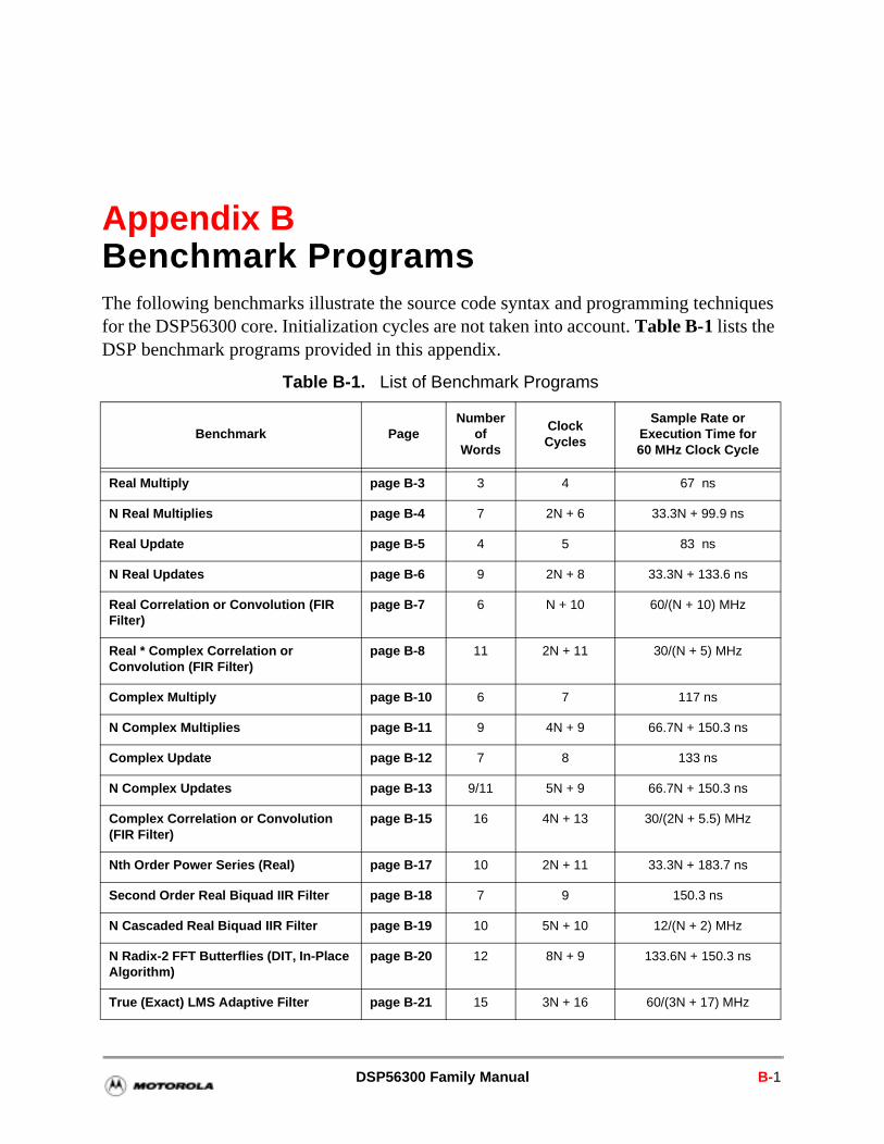
Appendix BBenchmark ProgramsThe following benchmarks illustrate the source code syntax and programming techniques for the DSP56300 core. Initialization cycles are not taken into account. Table B-1 lists the DSP benchmark programs provided in this appendix.
Table B-1. List of Benchmark Programs
Benchmark PageNumber
of Words
ClockCycles
Sample Rate or Execution Time for 60 MHz Clock Cycle
Real Multiply page B-3 3 4 67 ns
N Real Multiplies page B-4 7 2N + 6 33.3N + 99.9 ns
Real Update page B-5 4 5 83 ns
N Real Updates page B-6 9 2N + 8 33.3N + 133.6 ns
Real Correlation or Convolution (FIR Filter)
page B-7 6 N + 10 60/(N + 10) MHz
Real * Complex Correlation or Convolution (FIR Filter)
page B-8 11 2N + 11 30/(N + 5) MHz
Complex Multiply page B-10 6 7 117 ns
N Complex Multiplies page B-11 9 4N + 9 66.7N + 150.3 ns
Complex Update page B-12 7 8 133 ns
N Complex Updates page B-13 9/11 5N + 9 66.7N + 150.3 ns
Complex Correlation or Convolution (FIR Filter)
page B-15 16 4N + 13 30/(2N + 5.5) MHz
Nth Order Power Series (Real) page B-17 10 2N + 11 33.3N + 183.7 ns
Second Order Real Biquad IIR Filter page B-18 7 9 150.3 ns
N Cascaded Real Biquad IIR Filter page B-19 10 5N + 10 12/(N + 2) MHz
N Radix-2 FFT Butterflies (DIT, In-Place Algorithm)
page B-20 12 8N + 9 133.6N + 150.3 ns
True (Exact) LMS Adaptive Filter page B-21 15 3N + 16 60/(3N + 17) MHz
DSP56300 Family Manual B-1
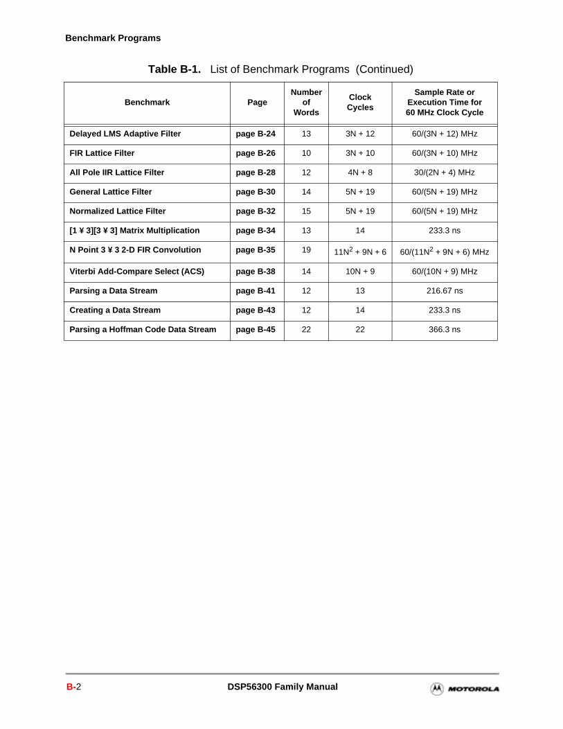
Benchmark Programs
Delayed LMS Adaptive Filter page B-24 13 3N + 12 60/(3N + 12) MHz
FIR Lattice Filter page B-26 10 3N + 10 60/(3N + 10) MHz
All Pole IIR Lattice Filter page B-28 12 4N + 8 30/(2N + 4) MHz
General Lattice Filter page B-30 14 5N + 19 60/(5N + 19) MHz
Normalized Lattice Filter page B-32 15 5N + 19 60/(5N + 19) MHz
[1 ¥ 3][3 ¥ 3] Matrix Multiplication page B-34 13 14 233.3 ns
N Point 3 ¥ 3 2-D FIR Convolution page B-35 19 11N2 + 9N + 6 60/(11N2 + 9N + 6) MHz
Viterbi Add-Compare Select (ACS) page B-38 14 10N + 9 60/(10N + 9) MHz
Parsing a Data Stream page B-41 12 13 216.67 ns
Creating a Data Stream page B-43 12 14 233.3 ns
Parsing a Hoffman Code Data Stream page B-45 22 22 366.3 ns
Table B-1. List of Benchmark Programs (Continued)
Benchmark PageNumber
of Words
ClockCycles
Sample Rate or Execution Time for 60 MHz Clock Cycle
B-2 DSP56300 Family Manual
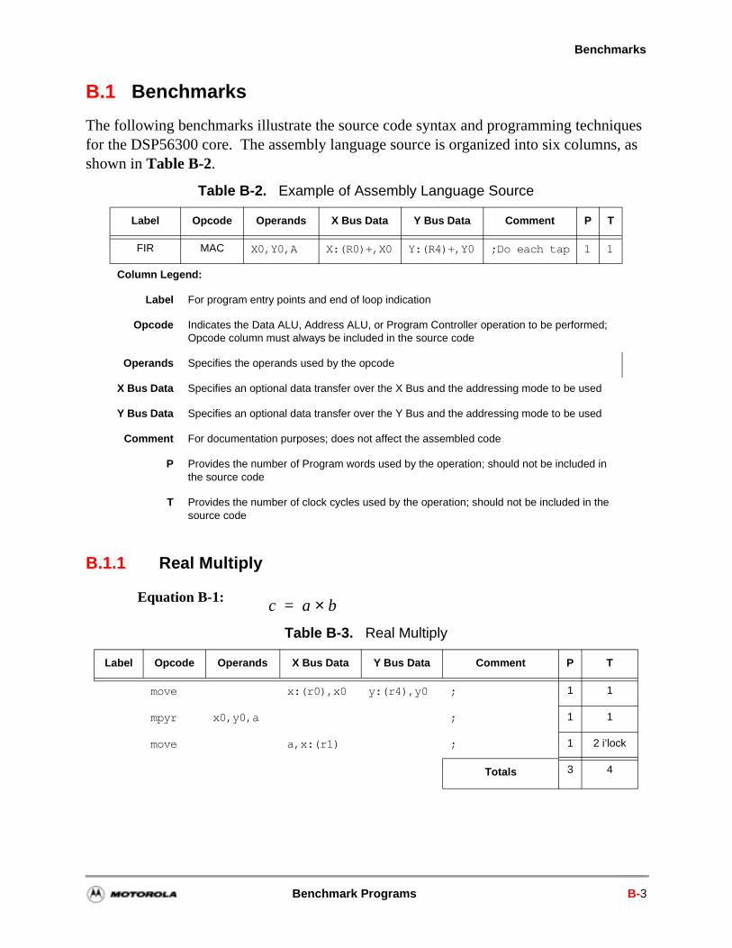
Benchmarks
B.1 Benchmarks
The following benchmarks illustrate the source code syntax and programming techniques for the DSP56300 core. The assembly language source is organized into six columns, as shown in Table B-2.
B.1.1 Real Multiply
Equation B-1:
Table B-2. Example of Assembly Language Source
Label Opcode Operands X Bus Data Y Bus Data Comment P T
FIR MAC X0,Y0,A X:(R0)+,X0 Y:(R4)+,Y0 ;Do each tap 1 1
Column Legend:
Label For program entry points and end of loop indication
Opcode Indicates the Data ALU, Address ALU, or Program Controller operation to be performed; Opcode column must always be included in the source code
Operands Specifies the operands used by the opcode
X Bus Data Specifies an optional data transfer over the X Bus and the addressing mode to be used
Y Bus Data Specifies an optional data transfer over the Y Bus and the addressing mode to be used
Comment For documentation purposes; does not affect the assembled code
P Provides the number of Program words used by the operation; should not be included in the source code
T Provides the number of clock cycles used by the operation; should not be included in the source code
Table B-3. Real Multiply
Label Opcode Operands X Bus Data Y Bus Data Comment P T
move x:(r0),x0 y:(r4),y0 ; 1 1
mpyr x0,y0,a ; 1 1
move a,x:(r1) ; 1 2 i’lock
Totals 3 4
c a b×=
Benchmark Programs B-3
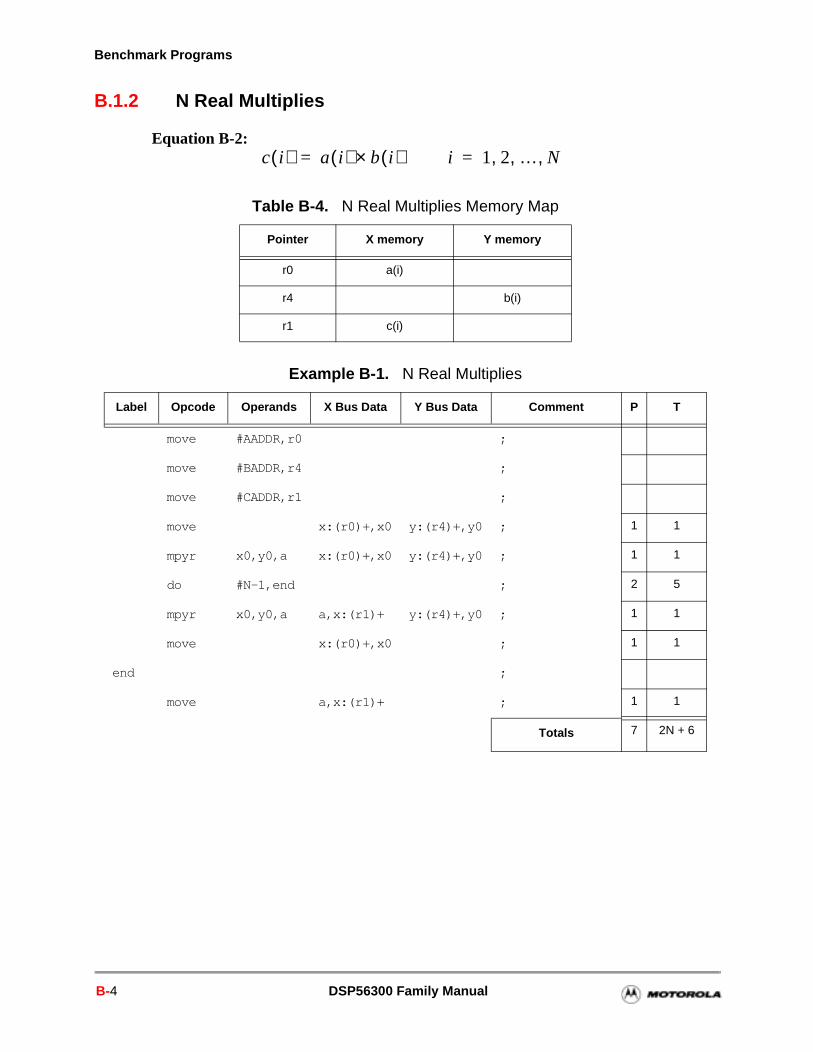
Benchmark Programs
B.1.2 N Real Multiplies
Equation B-2:
Table B-4. N Real Multiplies Memory Map
Pointer X memory Y memory
r0 a(i)
r4 b(i)
r1 c(i)
Example B-1. N Real Multiplies
Label Opcode Operands X Bus Data Y Bus Data Comment P T
move #AADDR,r0 ;
move #BADDR,r4 ;
move #CADDR,r1 ;
move x:(r0)+,x0 y:(r4)+,y0 ; 1 1
mpyr x0,y0,a x:(r0)+,x0 y:(r4)+,y0 ; 1 1
do #N-1,end ; 2 5
mpyr x0,y0,a a,x:(r1)+ y:(r4)+,y0 ; 1 1
move x:(r0)+,x0 ; 1 1
end ;
move a,x:(r1)+ ; 1 1
Totals 7 2N + 6
c i( ) a i( ) b i( )× i 1 2 … N, , ,==
B-4 DSP56300 Family Manual
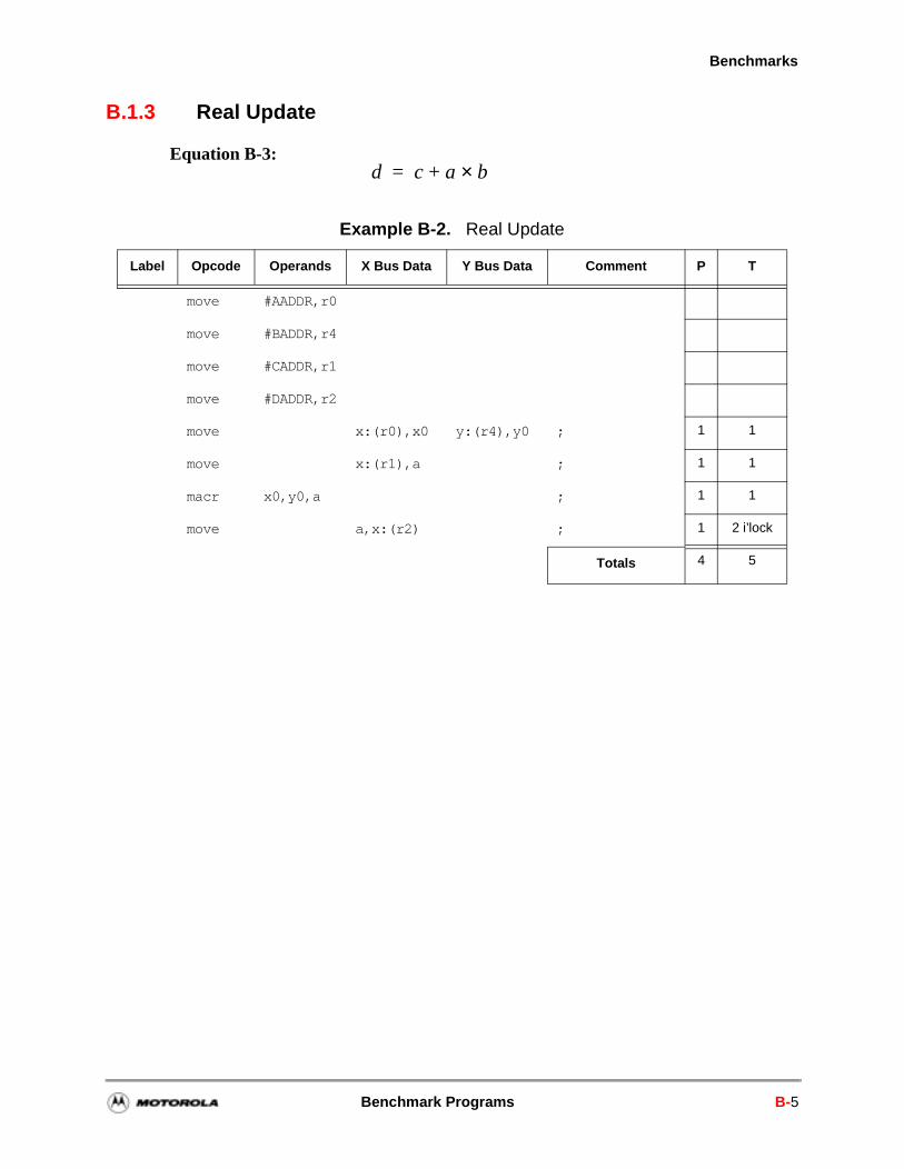
Benchmarks
B.1.3 Real Update
Equation B-3:
Example B-2. Real Update
Label Opcode Operands X Bus Data Y Bus Data Comment P T
move #AADDR,r0
move #BADDR,r4
move #CADDR,r1
move #DADDR,r2
move x:(r0),x0 y:(r4),y0 ; 1 1
move x:(r1),a ; 1 1
macr x0,y0,a ; 1 1
move a,x:(r2) ; 1 2 i’lock
Totals 4 5
d c a b×+=
Benchmark Programs B-5
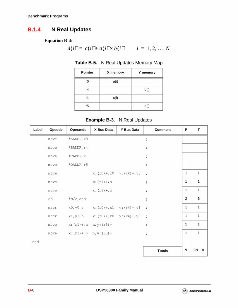
Benchmark Programs
B.1.4 N Real Updates
Equation B-4:
Table B-5. N Real Updates Memory Map
Pointer X memory Y memory
r0 a(i)
r4 b(i)
r1 c(i)
r5 d(i)
Example B-3. N Real Updates
Label Opcode Operands X Bus Data Y Bus Data Comment P T
move #AADDR,r0 ;
move #BADDR,r4 ;
move #CADDR,r1 ;
move #DADDR,r5 ;
move x:(r0)+,x0 y:(r4)+,y0 ; 1 1
move x:(r1)+,a ; 1 1
move x:(r1)+,b ; 1 1
do #N/2,end ; 2 5
macr x0,y0,a x:(r0)+,x1 y:(r4)+,y1 ; 1 1
macr x1,y1,b x:(r0)+,x0 y:(r4)+,y0 ; 1 1
move x:(r1)+,a a,y:(r5)+ ; 1 1
move x:(r1)+,b b,y:(r5)+ ; 1 1
end
Totals 9 2N + 8
d i( ) c i( ) a i( ) b i( )×+= i 1 2 … N, , ,=
B-6 DSP56300 Family Manual
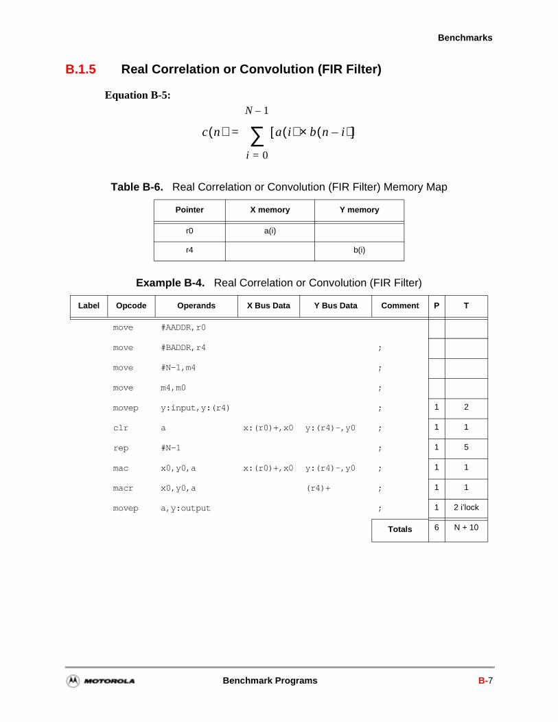
Benchmarks
B.1.5 Real Correlation or Convolution (FIR Filter)
Equation B-5:
Table B-6. Real Correlation or Convolution (FIR Filter) Memory Map
Pointer X memory Y memory
r0 a(i)
r4 b(i)
Example B-4. Real Correlation or Convolution (FIR Filter)
Label Opcode Operands X Bus Data Y Bus Data Comment P T
move #AADDR,r0
move #BADDR,r4 ;
move #N-1,m4 ;
move m4,m0 ;
movep y:input,y:(r4) ; 1 2
clr a x:(r0)+,x0 y:(r4)-,y0 ; 1 1
rep #N-1 ; 1 5
mac x0,y0,a x:(r0)+,x0 y:(r4)-,y0 ; 1 1
macr x0,y0,a (r4)+ ; 1 1
movep a,y:output ; 1 2 i’lock
Totals 6 N + 10
c n( ) a i( ) b n i–( )×[ ]
i 0=
N 1–
∑=
Benchmark Programs B-7
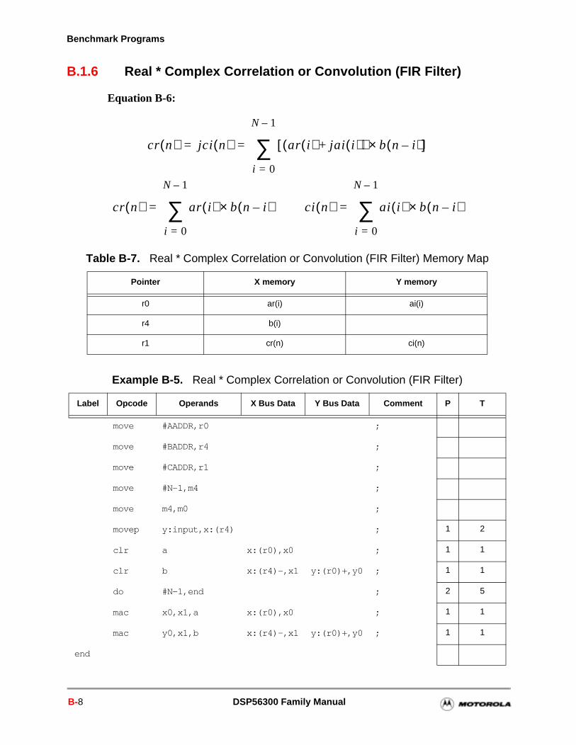
Benchmark Programs
B.1.6 Real * Complex Correlation or Convolution (FIR Filter)
Equation B-6:
Table B-7. Real * Complex Correlation or Convolution (FIR Filter) Memory Map
Pointer X memory Y memory
r0 ar(i) ai(i)
r4 b(i)
r1 cr(n) ci(n)
Example B-5. Real * Complex Correlation or Convolution (FIR Filter)
Label Opcode Operands X Bus Data Y Bus Data Comment P T
move #AADDR,r0 ;
move #BADDR,r4 ;
move #CADDR,r1 ;
move #N-1,m4 ;
move m4,m0 ;
movep y:input,x:(r4) ; 1 2
clr a x:(r0),x0 ; 1 1
clr b x:(r4)-,x1 y:(r0)+,y0 ; 1 1
do #N-1,end ; 2 5
mac x0,x1,a x:(r0),x0 ; 1 1
mac y0,x1,b x:(r4)-,x1 y:(r0)+,y0 ; 1 1
end
cr n( ) jci n( ) ar i( ) jai i( )+( ) b n i–( )×[ ]
i 0=
N 1–
∑= =
cr n( ) ar i( ) b n i–( )×
i 0=
N 1–
∑= ci n( ) ai i( ) b n i–( )×
i 0=
N 1–
∑=
B-8 DSP56300 Family Manual
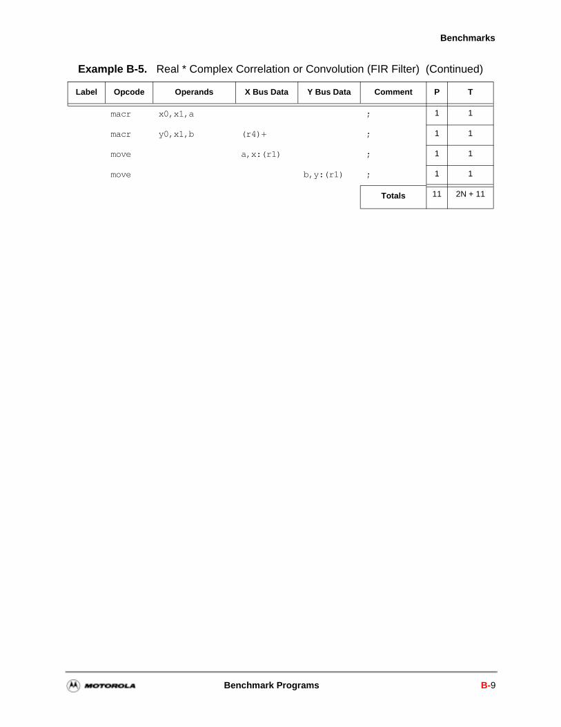
Benchmarks
Label Opcode Operands X Bus Data Y Bus Data Comment P T
macr x0,x1,a ; 1 1
macr y0,x1,b (r4)+ ; 1 1
move a,x:(r1) ; 1 1
move b,y:(r1) ; 1 1
Totals 11 2N + 11
Example B-5. Real * Complex Correlation or Convolution (FIR Filter) (Continued)
Benchmark Programs B-9
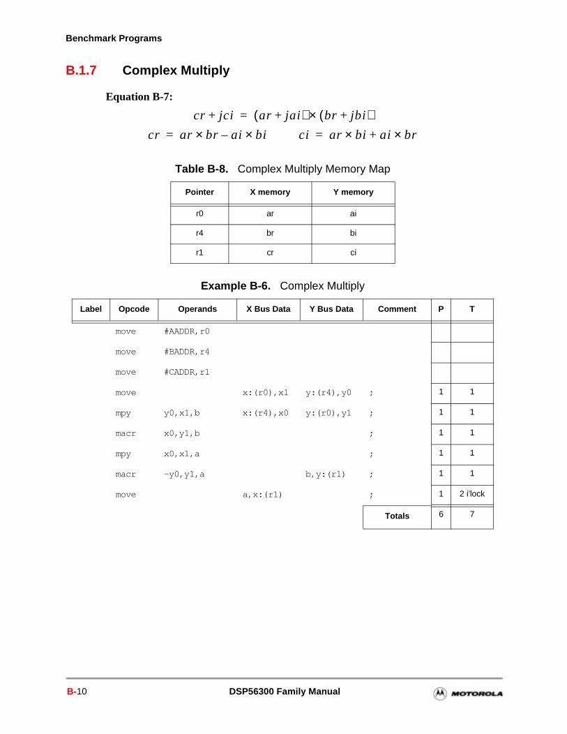
Benchmark Programs
B.1.7 Complex Multiply
Equation B-7:
Table B-8. Complex Multiply Memory Map
Pointer X memory Y memory
r0 ar ai
r4 br bi
r1 cr ci
Example B-6. Complex Multiply
Label Opcode Operands X Bus Data Y Bus Data Comment P T
move #AADDR,r0
move #BADDR,r4
move #CADDR,r1
move x:(r0),x1 y:(r4),y0 ; 1 1
mpy y0,x1,b x:(r4),x0 y:(r0),y1 ; 1 1
macr x0,y1,b ; 1 1
mpy x0,x1,a ; 1 1
macr -y0,y1,a b,y:(r1) ; 1 1
move a,x:(r1) ; 1 2 i’lock
Totals 6 7
cr jci+ ar jai+( ) br jbi+( )×=
cr ar br ai bi×–×= ci ar bi ai br×+×=
B-10 DSP56300 Family Manual
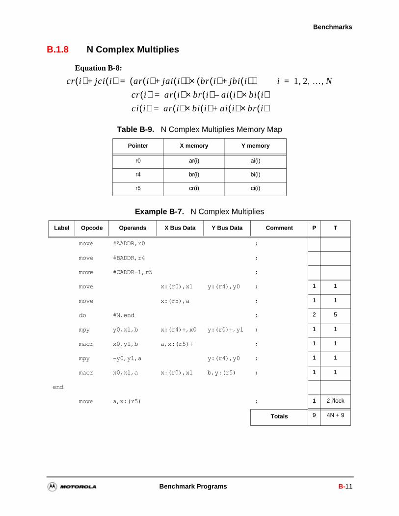
Benchmarks
B.1.8 N Complex Multiplies
Equation B-8:
Table B-9. N Complex Multiplies Memory Map
Pointer X memory Y memory
r0 ar(i) ai(i)
r4 br(i) bi(i)
r5 cr(i) ci(i)
Example B-7. N Complex Multiplies
Label Opcode Operands X Bus Data Y Bus Data Comment P T
move #AADDR,r0 ;
move #BADDR,r4 ;
move #CADDR-1,r5 ;
move x:(r0),x1 y:(r4),y0 ; 1 1
move x:(r5),a ; 1 1
do #N,end ; 2 5
mpy y0,x1,b x:(r4)+,x0 y:(r0)+,y1 ; 1 1
macr x0,y1,b a,x:(r5)+ ; 1 1
mpy -y0,y1,a y:(r4),y0 ; 1 1
macr x0,x1,a x:(r0),x1 b,y:(r5) ; 1 1
end
move a,x:(r5) ; 1 2 i’lock
Totals 9 4N + 9
cr i( ) jci i( )+ ar i( ) jai i( )+( ) br i( ) jbi i( )+( )×= i 1 2 … N, , ,=
cr i( ) ar i( ) br i( ) ai i( ) bi× i( )–×=
ci i( ) ar i( ) bi i( ) ai i( ) br×+× i( )=
Benchmark Programs B-11
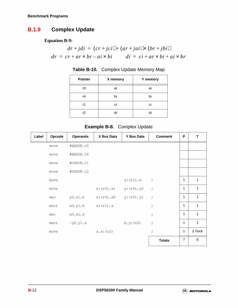
Benchmark Programs
B.1.9 Complex Update
Equation B-9:
Table B-10. Complex Update Memory Map
Pointer X memory Y memory
r0 ar ai
r4 br bi
r1 cr ci
r2 dr di
Example B-8. Complex Update
Label Opcode Operands X Bus Data Y Bus Data Comment P T
move #AADDR,r0
move #BADDR,r4
move #CADDR,r1
move #DADDR,r2
move y:(r1),b ; 1 1
move x:(r0),x1 y:(r4),y0 ; 1 1
mac y0,x1,b x:(r4),x0 y:(r0),y1 ; 1 1
macr x0,y1,b x:(r1),a ; 1 1
mac x0,x1,a ; 1 1
macr -y0,y1,a b,y:(r2) ; 1 1
move a,x:(r2) ; 1 2 i’lock
Totals 7 8
dr jdi+ cr jci+( ) ar jai+( ) br jbi+( )×+=
dr cr ar br ai bi×–×+= di ci ar bi ai br×+×+=
B-12 DSP56300 Family Manual
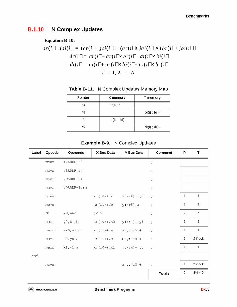
Benchmarks
B.1.10 N Complex Updates
Equation B-10:
Table B-11. N Complex Updates Memory Map
Pointer X memory Y memory
r0 ar(i) ; ai(i)
r4 br(i) ; bi(i)
r1 cr(i) ; ci(i)
r5 dr(i) ; di(i)
Example B-9. N Complex Updates
Label Opcode Operands X Bus Data Y Bus Data Comment P T
move #AADDR,r0 ;
move #BADDR,r4 ;
move #CADDR,r1 ;
move #DADDR-1,r5 ;
move x:(r0)+,x1 y:(r4)+,y0 ; 1 1
move x:(r1)+,b y:(r5),a ; 1 1
do #N,end ;2 5 ; 2 5
mac y0,x1,b x:(r0)+,x0 y:(r4)+,y1 ; 1 1
macr -x0,y1,b x:(r1)+,a a,y:(r5)+ ; 1 1
mac x0,y0,a x:(r1)+,b b,y:(r5)+ ; 1 2 i’lock
macr x1,y1,a x:(r0)+,x1 y:(r4)+,y0 ; 1 1
end
move a,y:(r5)+ ; 1 2 i’lock
Totals 9 5N + 9
dr i( ) jdi i( )+ cr i( ) jci i( )+( ) ar i( ) jai i( )+( ) br i( ) jbi i( )+( )×+=
dr i( ) cr i( ) ar i( ) br i( ) ai i( ) bi× i( )–×+=
di i( ) ci i( ) ar i( ) bi i( ) ai i( ) br× i( )+×+=
i 1 2 … N, , ,=
Benchmark Programs B-13
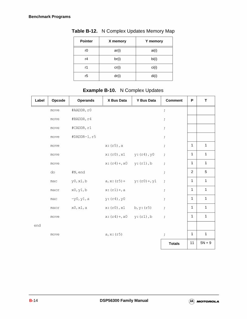
Benchmark Programs
Table B-12. N Complex Updates Memory Map
Pointer X memory Y memory
r0 ar(i) ai(i)
r4 br(i) bi(i)
r1 cr(i) ci(i)
r5 dr(i) di(i)
Example B-10. N Complex Updates
Label Opcode Operands X Bus Data Y Bus Data Comment P T
move #AADDR,r0 ;
move #BADDR,r4 ;
move #CADDR,r1 ;
move #DADDR-1,r5 ;
move x:(r5),a ; 1 1
move x:(r0),x1 y:(r4),y0 ; 1 1
move x:(r4)+,x0 y:(r1),b ; 1 1
do #N,end ; 2 5
mac y0,x1,b a,x:(r5)+ y:(r0)+,y1 ; 1 1
macr x0,y1,b x:(r1)+,a ; 1 1
mac -y0,y1,a y:(r4),y0 ; 1 1
macr x0,x1,a x:(r0),x1 b,y:(r5) ; 1 1
move x:(r4)+,x0 y:(r1),b ; 1 1
end
move a,x:(r5) ; 1 1
Totals 11 5N + 9
B-14 DSP56300 Family Manual
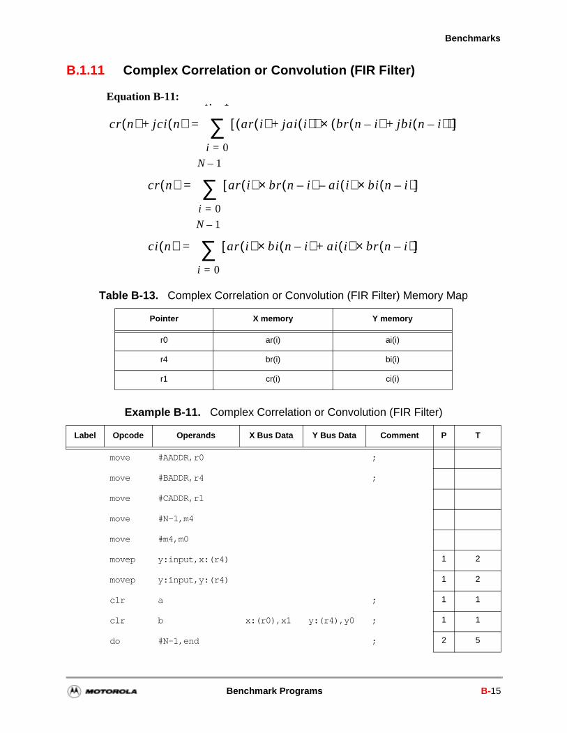
Benchmarks
B.1.11 Complex Correlation or Convolution (FIR Filter)
Equation B-11:
Table B-13. Complex Correlation or Convolution (FIR Filter) Memory Map
Pointer X memory Y memory
r0 ar(i) ai(i)
r4 br(i) bi(i)
r1 cr(i) ci(i)
Example B-11. Complex Correlation or Convolution (FIR Filter)
Label Opcode Operands X Bus Data Y Bus Data Comment P T
move #AADDR,r0 ;
move #BADDR,r4 ;
move #CADDR,r1
move #N-1,m4
move #m4,m0
movep y:input,x:(r4) 1 2
movep y:input,y:(r4) 1 2
clr a ; 1 1
clr b x:(r0),x1 y:(r4),y0 ; 1 1
do #N-1,end ; 2 5
cr n( ) jci n( )+ ar i( ) jai i( )+( ) br n i–( ) jbi n i–( )+( )×[ ]
i 0=
N 1
∑=
cr n( ) ar i( ) br n i–( ) ai i( ) bi n i–( )×–×[ ]
i 0=
N 1–
∑=
ci n( ) ar i( ) bi n i–( ) ai i( ) br n i–( )×+×[ ]
i 0=
N 1–
∑=
Benchmark Programs B-15
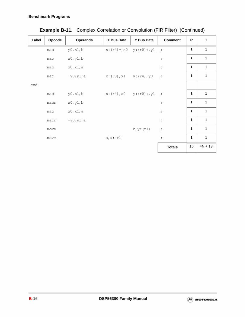
Benchmark Programs
Label Opcode Operands X Bus Data Y Bus Data Comment P T
mac y0,x1,b x:(r4)-,x0 y:(r0)+,y1 ; 1 1
mac x0,y1,b ; 1 1
mac x0,x1,a ; 1 1
mac -y0,y1,a x:(r0),x1 y:(r4),y0 ; 1 1
end
mac y0,x1,b x:(r4),x0 y:(r0)+,y1 ; 1 1
macr x0,y1,b ; 1 1
mac x0,x1,a ; 1 1
macr -y0,y1,a ; 1 1
move b,y:(r1) ; 1 1
move a,x:(r1) ; 1 1
Totals 16 4N + 13
Example B-11. Complex Correlation or Convolution (FIR Filter) (Continued)
B-16 DSP56300 Family Manual
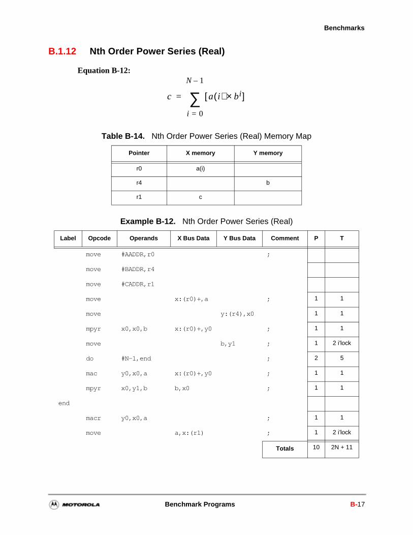
Benchmarks
B.1.12 Nth Order Power Series (Real)
Equation B-12:
Table B-14. Nth Order Power Series (Real) Memory Map
Pointer X memory Y memory
r0 a(i)
r4 b
r1 c
Example B-12. Nth Order Power Series (Real)
Label Opcode Operands X Bus Data Y Bus Data Comment P T
move #AADDR,r0 ;
move #BADDR,r4
move #CADDR,r1
move x:(r0)+,a ; 1 1
move y:(r4),x0 1 1
mpyr x0,x0,b x:(r0)+,y0 ; 1 1
move b,y1 ; 1 2 i’lock
do #N-1,end ; 2 5
mac y0,x0,a x:(r0)+,y0 ; 1 1
mpyr x0,y1,b b,x0 ; 1 1
end
macr y0,x0,a ; 1 1
move a,x:(r1) ; 1 2 i’lock
Totals 10 2N + 11
c a i( ) bi×[ ]
i 0=
N 1–
∑=
Benchmark Programs B-17
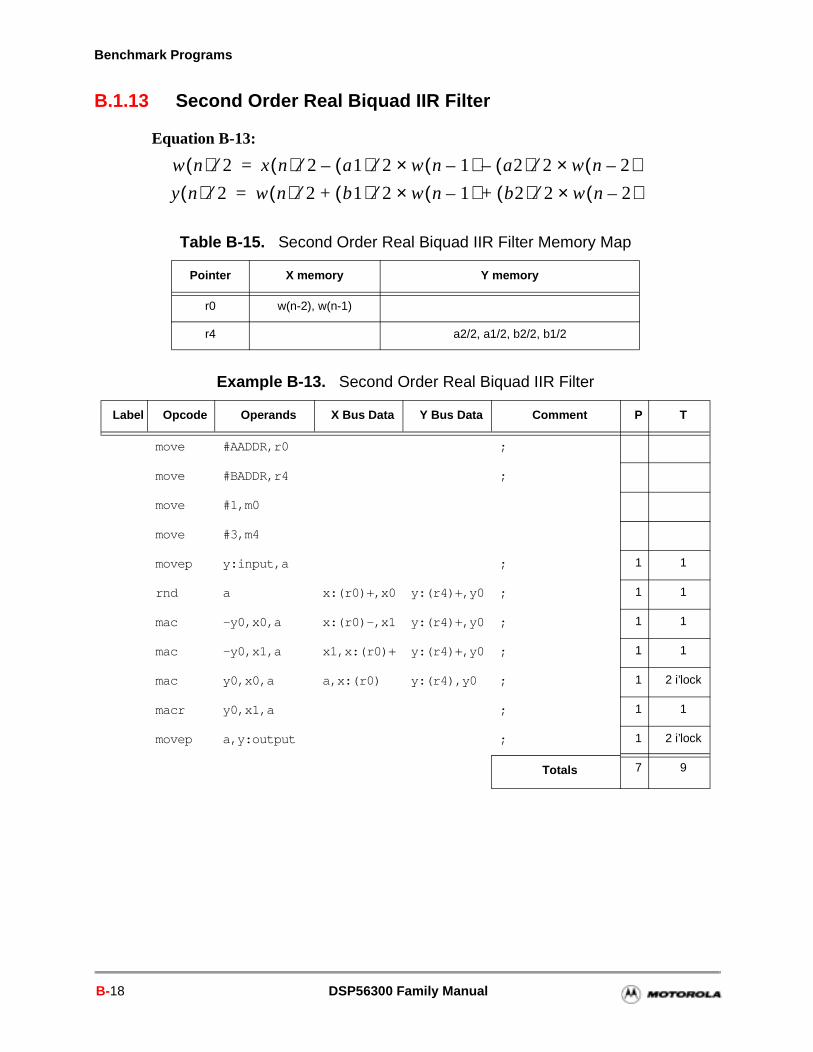
Benchmark Programs
B.1.13 Second Order Real Biquad IIR Filter
Equation B-13:
Table B-15. Second Order Real Biquad IIR Filter Memory Map
Pointer X memory Y memory
r0 w(n-2), w(n-1)
r4 a2/2, a1/2, b2/2, b1/2
Example B-13. Second Order Real Biquad IIR Filter
Label Opcode Operands X Bus Data Y Bus Data Comment P T
move #AADDR,r0 ;
move #BADDR,r4 ;
move #1,m0
move #3,m4
movep y:input,a ; 1 1
rnd a x:(r0)+,x0 y:(r4)+,y0 ; 1 1
mac -y0,x0,a x:(r0)-,x1 y:(r4)+,y0 ; 1 1
mac -y0,x1,a x1,x:(r0)+ y:(r4)+,y0 ; 1 1
mac y0,x0,a a,x:(r0) y:(r4),y0 ; 1 2 i’lock
macr y0,x1,a ; 1 1
movep a,y:output ; 1 2 i’lock
Totals 7 9
w n( ) 2⁄ x n( ) 2⁄ a1( ) 2⁄ w n 1–( ) a2( ) 2⁄–× w n 2–( )×–=
y n( ) 2⁄ w n( ) 2⁄ b1( ) 2⁄ w n 1–( ) b2( ) 2⁄+× w n 2–( )×+=
B-18 DSP56300 Family Manual
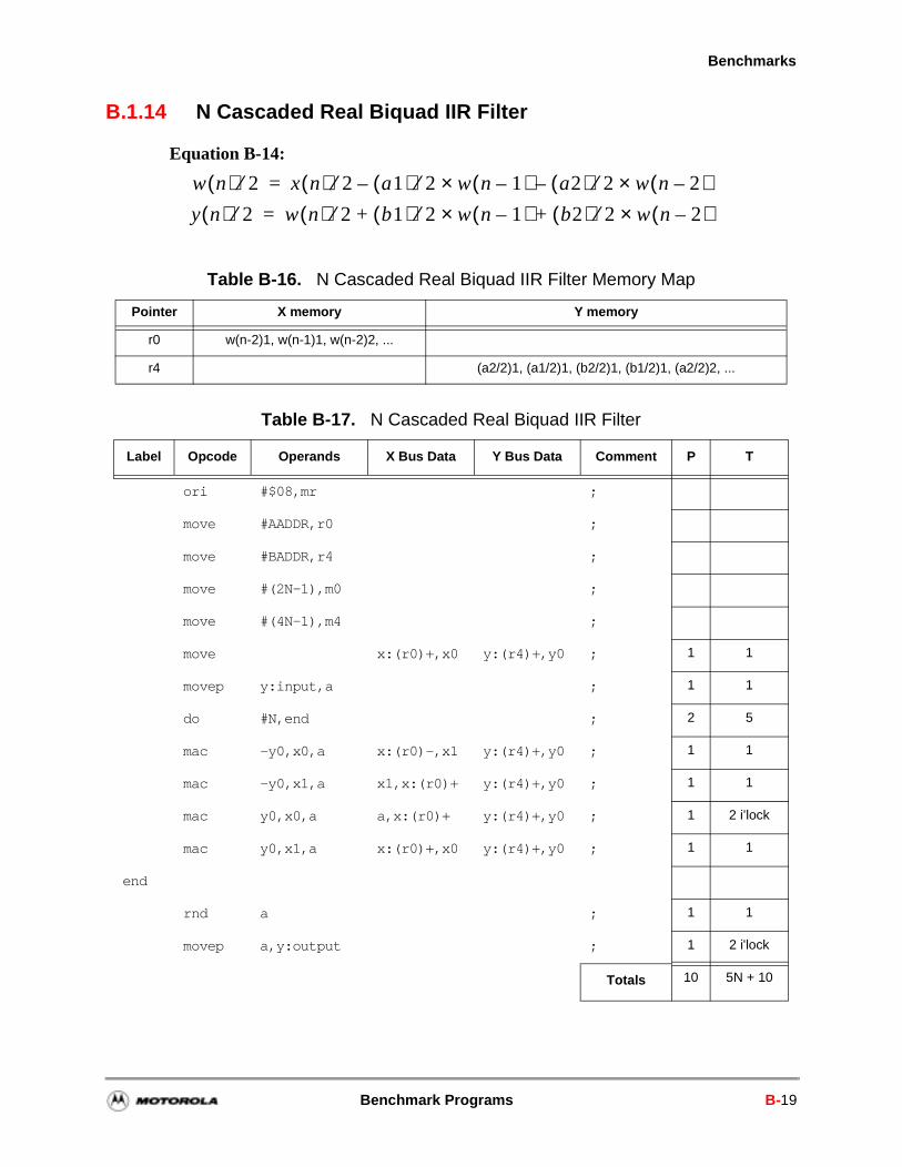
Benchmarks
B.1.14 N Cascaded Real Biquad IIR Filter
Equation B-14:
Table B-16. N Cascaded Real Biquad IIR Filter Memory Map
Pointer X memory Y memory
r0 w(n-2)1, w(n-1)1, w(n-2)2, ...
r4 (a2/2)1, (a1/2)1, (b2/2)1, (b1/2)1, (a2/2)2, ...
Table B-17. N Cascaded Real Biquad IIR Filter
Label Opcode Operands X Bus Data Y Bus Data Comment P T
ori #$08,mr ;
move #AADDR,r0 ;
move #BADDR,r4 ;
move #(2N-1),m0 ;
move #(4N-1),m4 ;
move x:(r0)+,x0 y:(r4)+,y0 ; 1 1
movep y:input,a ; 1 1
do #N,end ; 2 5
mac -y0,x0,a x:(r0)-,x1 y:(r4)+,y0 ; 1 1
mac -y0,x1,a x1,x:(r0)+ y:(r4)+,y0 ; 1 1
mac y0,x0,a a,x:(r0)+ y:(r4)+,y0 ; 1 2 i’lock
mac y0,x1,a x:(r0)+,x0 y:(r4)+,y0 ; 1 1
end
rnd a ; 1 1
movep a,y:output ; 1 2 i'lock
Totals 10 5N + 10
w n( ) 2⁄ x n( ) 2⁄ a1( ) 2⁄ w n 1–( ) a2( ) 2⁄–× w n 2–( )×–=
y n( ) 2⁄ w n( ) 2⁄ b1( ) 2⁄ w n 1–( ) b2( ) 2⁄+× w n 2–( )×+=
Benchmark Programs B-19
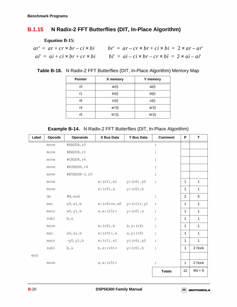
Benchmark Programs
B.1.15 N Radix-2 FFT Butterflies (DIT, In-Place Algorithm)
Equation B-15:
Table B-18. N Radix-2 FFT Butterflies (DIT, In-Place Algorithm) Memory Map
Pointer X memory Y memory
r0 ar(i) ai(i)
r1 br(i) bi(i)
r6 cr(i) ci(i)
r4 ar’(i) ai’(i)
r5 br’(i) bi’(i)
Example B-14. N Radix-2 FFT Butterflies (DIT, In-Place Algorithm)
Label Opcode Operands X Bus Data Y Bus Data Comment P T
move #AADDR,r0 ;
move #BADDR,r1 ;
move #CADDR,r6 ;
move #ATADDR,r4 ;
move #BTADDR-1,r5 ;
move x:(r1),x1 y:(r6),y0 ; 1 1
move x:(r5),a y:(r0),b 1 1
do #N,end ; 2 5
mac y0,x1,b x:(r6)+n,x0 y:(r1)+,y1 ; 1 1
macr x0,y1,b a,x:(r5)+ y:(r0),a ; 1 1
subl b,a ; 1 1
move x:(r0),b b,y:(r4) ; 1 1
mac x0,x1,b x:(r0)+,a a,y:(r5) ; 1 1
macr -y0,y1,b x:(r1),x1 y:(r6),y0 ; 1 1
subl b,a b,x:(r4)+ y:(r0),b ; 1 2 i'lock
end
move a,x:(r5)+ ; 1 2 i'lock
Totals 12 8N + 9
ar’ ar cr br ci bi×–×+= br' ar cr br ci bi×+×– 2 ar a–× r'= =
ai' ai ci br cr bi×+×+= bi' ai ci br cr bi×–×– 2 ai a–× i'= =
B-20 DSP56300 Family Manual
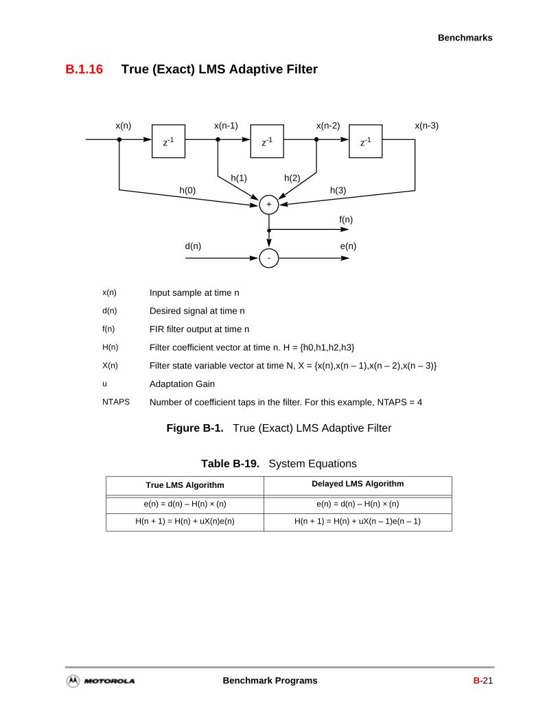
Benchmarks
B.1.16 True (Exact) LMS Adaptive Filter
Figure B-1. True (Exact) LMS Adaptive Filter
Table B-19. System Equations
True LMS Algorithm Delayed LMS Algorithm
e(n) = d(n) – H(n) × (n) e(n) = d(n) – H(n) × (n)
H(n + 1) = H(n) + uX(n)e(n) H(n + 1) = H(n) + uX(n – 1)e(n – 1)
x(n) x(n-1) x(n-2) x(n-3)
z-1 z-1 z-1
d(n)
f(n)
e(n)
h(1) h(2)h(3)h(0)
-
+
x(n) Input sample at time n
d(n) Desired signal at time n
f(n) FIR filter output at time n
H(n) Filter coefficient vector at time n. H = h0,h1,h2,h3
X(n) Filter state variable vector at time N, X = x(n),x(n – 1),x(n – 2),x(n – 3)
u Adaptation Gain
NTAPS Number of coefficient taps in the filter. For this example, NTAPS = 4
Benchmark Programs B-21
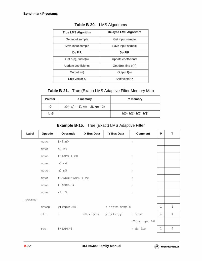
Benchmark Programs
Table B-20. LMS Algorithms
True LMS Algorithm Delayed LMS Algorithm
Get input sample Get input sample
Save input sample Save input sample
Do FIR Do FIR
Get d(n), find e(n) Update coefficients
Update coefficients Get d(n), find e(n)
Output f(n) Output f(n)
Shift vector X Shift vector X
Table B-21. True (Exact) LMS Adaptive Filter Memory Map
Pointer X memory Y memory
r0 x(n), x(n – 1), x(n – 2), x(n – 3)
r4, r5 h(0), h(1), h(2), h(3)
Example B-15. True (Exact) LMS Adaptive Filter
Label Opcode Operands X Bus Data Y Bus Data Comment P T
move #-2,n0 ;
move n0,n4
move #NTAPS-1,m0 ;
move m0,m4 ;
move m0,m5 ;
move #AADDR+NTAPS-1,r0 ;
move #BADDR,r4 ;
move r4,r5 ;
_getsmp
movep y:input,x0 ; input sample 1 1
clr a x0,x:(r0)+ y:(r4)+,y0 ; save 1 1
;X(n), get h0
rep #NTAPS-1 ; do fir 1 5
B-22 DSP56300 Family Manual
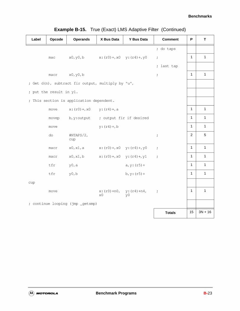
Benchmarks
Label Opcode Operands X Bus Data Y Bus Data Comment P T
; do taps
mac x0,y0,b x:(r0)+,x0 y:(r4)+,y0 ; 1 1
; last tap
macr x0,y0,b ; 1 1
; Get d(n), subtract fir output, multiply by "u",
; put the result in y1.
; This section is application dependent.
move x:(r0)+,x0 y:(r4)+,a 1 1
movep b,y:output ; output fir if desired 1 1
move y:(r4)+,b 1 1
do #NTAPS/2,cup
; 2 5
macr x0,x1,a x:(r0)+,x0 y:(r4)+,y0 ; 1 1
macr x0,x1,b x:(r0)+,x0 y:(r4)+,y1 ; 1 1
tfr y0,a a,y:(r5)+ 1 1
tfr y0,b b,y:(r5)+ 1 1
cup
move x:(r0)+n0,x0
y:(r4)+n4,y0
; 1 1
; continue looping (jmp _getsmp)
Totals 15 3N + 16
Example B-15. True (Exact) LMS Adaptive Filter (Continued)
Benchmark Programs B-23
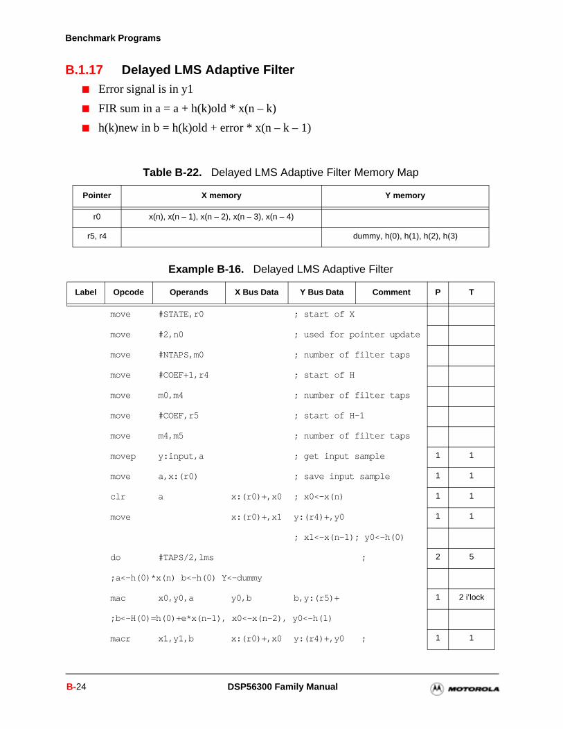
Benchmark Programs
B.1.17 Delayed LMS Adaptive Filter Error signal is in y1
FIR sum in a = a + h(k)old * x(n – k)
h(k)new in b = h(k)old + error * x(n – k – 1)
Table B-22. Delayed LMS Adaptive Filter Memory Map
Pointer X memory Y memory
r0 x(n), x(n – 1), x(n – 2), x(n – 3), x(n – 4)
r5, r4 dummy, h(0), h(1), h(2), h(3)
Example B-16. Delayed LMS Adaptive Filter
Label Opcode Operands X Bus Data Y Bus Data Comment P T
move #STATE,r0 ; start of X
move #2,n0 ; used for pointer update
move #NTAPS,m0 ; number of filter taps
move #COEF+1,r4 ; start of H
move m0,m4 ; number of filter taps
move #COEF,r5 ; start of H-1
move m4,m5 ; number of filter taps
movep y:input,a ; get input sample 1 1
move a,x:(r0) ; save input sample 1 1
clr a x:(r0)+,x0 ; x0<-x(n) 1 1
move x:(r0)+,x1 y:(r4)+,y0 1 1
; x1<-x(n-1); y0<-h(0)
do #TAPS/2,lms ; 2 5
;a<-h(0)*x(n) b<-h(0) Y<-dummy
mac x0,y0,a y0,b b,y:(r5)+ 1 2 i’lock
;b<-H(0)=h(0)+e*x(n-1), x0<-x(n-2), y0<-h(1)
macr x1,y1,b x:(r0)+,x0 y:(r4)+,y0 ; 1 1
B-24 DSP56300 Family Manual
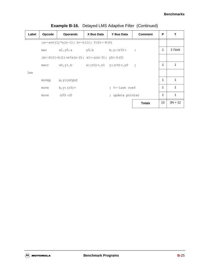
Benchmarks
Label Opcode Operands X Bus Data Y Bus Data Comment P T
;a<-a+h(1)*x(n-1); b<-h(1); Y(0)<-H(0)
mac x1,y0,a y0,b b,y:(r5)+ ; 1 2 i’lock
;b<-H(1)=h(1)+e*x(n-2); x1<-x(n-3); y0<-h(2)
macr x0,y1,b x:(r0)+,x1 y:(r4)+,y0 ; 1 1
lms
movep a,y:output 1 1
move b,y:(r5)+ ; Y<-last coef 1 1
move (r0)-n0 ; update pointer 1 1
Totals 13 3N + 12
Example B-16. Delayed LMS Adaptive Filter (Continued)
Benchmark Programs B-25
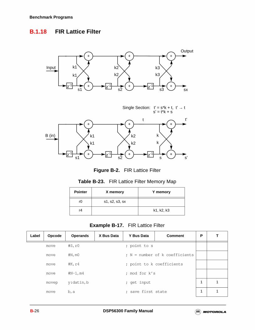
Benchmark Programs
B.1.18 FIR Lattice Filter
Figure B-2. FIR Lattice Filter
Table B-23. FIR Lattice Filter Memory Map
Pointer X memory Y memory
r0 s1, s2, s3, sx
r4 k1, k2, k3
Example B-17. FIR Lattice Filter
Label Opcode Operands X Bus Data Y Bus Data Comment P T
move #S,r0 ; point to s
move #N,m0 ; N = number of k coefficients
move #K,r4 ; point to k coefficients
move #N-1,m4 ; mod for k’s
movep y:datin,b ; get input 1 1
move b,a ; save first state 1 1
Input
z-1 z-1 z-1s2s1 s3 sx
Output
k1
k1
k2
k2
k3
k3
+ + +
+ + +
B (in)
t’t
Single Section: t’ = s*k + t, t’ → ts’ = t*k + s
z-1 z-1 z-1s2 s
k1
k1
k2
k2
+ + +
+ + +s1 s’
k
k
B-26 DSP56300 Family Manual
Benchmarks
Label Opcode Operands X Bus Data Y Bus Data Comment P T
move x:(r0),x0 y:(r4)+,y0 ; get s, get k 1 1
do #N,_elat ; 2 5
macr x0,y0,b b,y1 ; s*k+t,copy t ; for mul
1 1
tfr x0,a a,x:(r0)+ ; save s’, ; copy next s
1 1
macr y1,y0,a x:(r0),x0 y:(r4)+,y0 ; t*k+s, get s, ; get k
1 1
_elat
move a,x:(r0)+ y:(r4)-,y0 ; adj r4,; dummy load
1 1
movep b,y:datout ; output sample 1 1
Totals 10 3N + 10
Example B-17. FIR Lattice Filter (Continued)
Benchmark Programs B-27
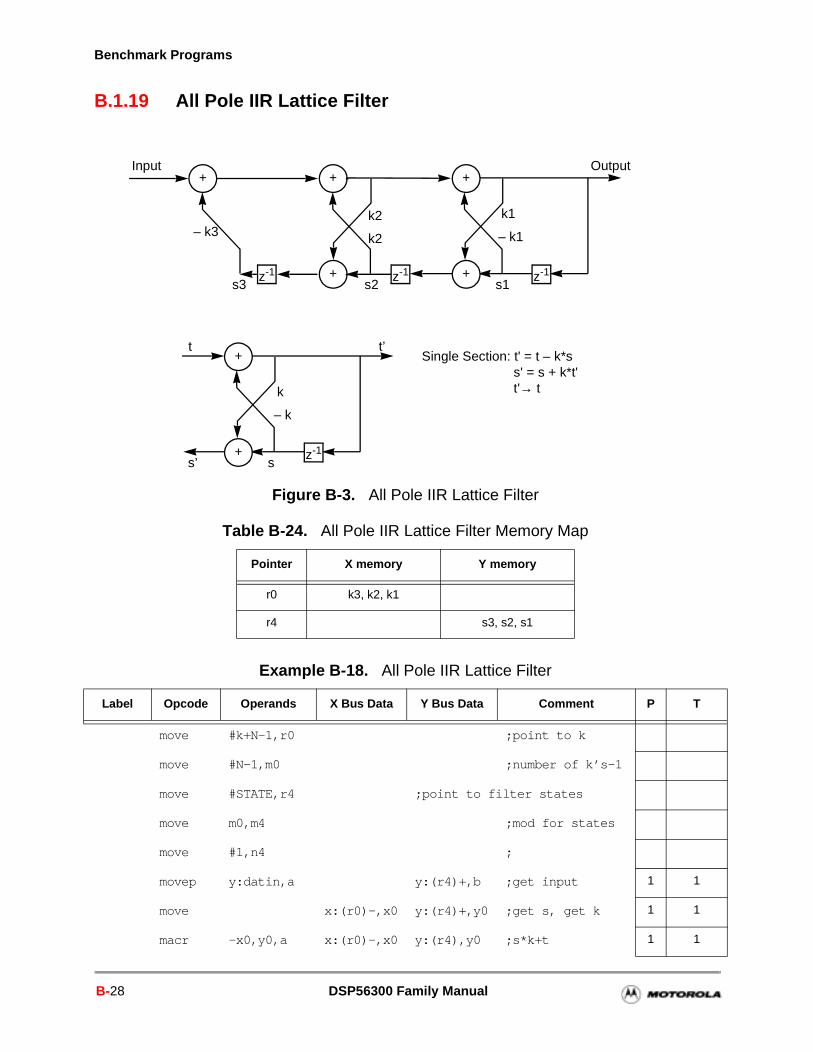
Benchmark Programs
B.1.19 All Pole IIR Lattice Filter
Figure B-3. All Pole IIR Lattice Filter
Table B-24. All Pole IIR Lattice Filter Memory Map
Pointer X memory Y memory
r0 k3, k2, k1
r4 s3, s2, s1
Example B-18. All Pole IIR Lattice Filter
Label Opcode Operands X Bus Data Y Bus Data Comment P T
move #k+N-1,r0 ;point to k
move #N-1,m0 ;number of k’s-1
move #STATE,r4 ;point to filter states
move m0,m4 ;mod for states
move #1,n4 ;
movep y:datin,a y:(r4)+,b ;get input 1 1
move x:(r0)-,x0 y:(r4)+,y0 ;get s, get k 1 1
macr -x0,y0,a x:(r0)-,x0 y:(r4),y0 ;s*k+t 1 1
t t’
s’
Single Section: t' = t – k*ss' = s + k*t't'→ t
Input Output
z-1 z-1s2 s1
– k3k2
k2
+ + +
+ +s3
k1
– k1
z-1
s
+
+
k
– k
z-1
B-28 DSP56300 Family Manual
Benchmarks
Label Opcode Operands X Bus Data Y Bus Data Comment P T
do #N-1,_endlat
;do sections 2 5
macr -x0,y0,a y:(r4)+,y1 ; 1 1
tfr y1,b a,x1 b,y:(r4) ; 1 2 i’lock
macr x1,x0,b x:(r0)-,x0 y:(r4),y0 1 1
_endlat
movep a,y:datout 1 1
move x:(r0)+,x0 y:(r4)+,r0 ;output sample 1 1
move b,y:(r4)+ ;save s’ 1 1
;save last s’, update r4
move a,y:(r4) 1 1
Totals 12 4N + 8
Example B-18. All Pole IIR Lattice Filter (Continued)
Benchmark Programs B-29
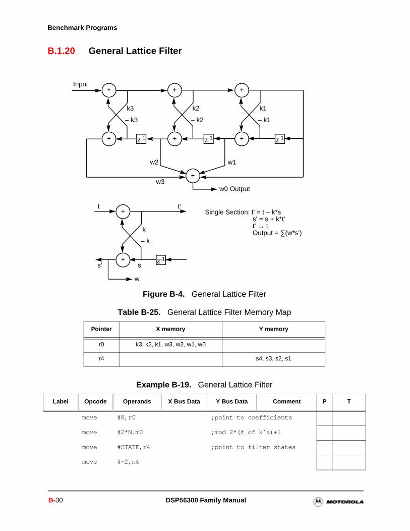
Benchmark Programs
B.1.20 General Lattice Filter
Figure B-4. General Lattice Filter
Table B-25. General Lattice Filter Memory Map
Pointer X memory Y memory
r0 k3, k2, k1, w3, w2, w1, w0
r4 s4, s3, s2, s1
Example B-19. General Lattice Filter
Label Opcode Operands X Bus Data Y Bus Data Comment P T
move #K,r0 ;point to coefficients
move #2*N,m0 ;mod 2*(# of k’s)+1
move #STATE,r4 ;point to filter states
move #-2,n4
t t’
s’
Input
w0 Output
z-1 z-1
+
+
w2
k1
– k1
z-1
s
+
+
k
– k
z-1
+
+
k2
– k2
+
+
k3
– k3
+w3
w1
w
Single Section: t' = t – k*ss' = s + k*t't' → tOutput = ∑(w*s')
B-30 DSP56300 Family Manual

Benchmarks
Label Opcode Operands X Bus Data Y Bus Data Comment P T
move #N,m4 ;mod on filter states
movep y:datin,a ;get input 1 1
move x:(r0)+,x0 y:(r4)-,y0 1 1
do #N,_endlat 2 5
macr -x0,y0,a ; 1 1
tfr y0,b a,x1 b,y:(r4)+n4 ; 1 2 i’lock
macr x1,x0,b x:(r0)+,x0 y:(r4)-,y0 ; 1 1
_endlat
move b,y:(r4)+ ;save s’ 1 2 i’lock
clr a a,y:(r4)+ ;save last s’, ; update r4
1 1
move y:(r4)+,y0 1 1
rep #N ; 1 5
mac x0,y0,a x:(r0)+,x0 y:(r4)+,y0 ;s*w+out, ; get s, get w
1 1
macr x0,y0,a ;last mac 1 1
movep a,y:datout ;output sample 1 2 i’lock
Totals 14 5N + 19
Example B-19. General Lattice Filter (Continued)
Benchmark Programs B-31
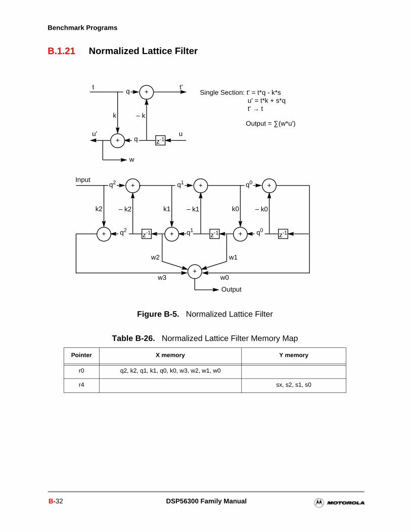
Benchmark Programs
B.1.21 Normalized Lattice Filter
Figure B-5. Normalized Lattice Filter
Table B-26. Normalized Lattice Filter Memory Map
Pointer X memory Y memory
r0 q2, k2, q1, k1, q0, k0, w3, w2, w1, w0
r4 sx, s2, s1, s0
t t’
Input
Output
w2
+
+
k – k
z-1
+w3
w1
w
q
u' uq
Single Section: t' = t*q - k*su' = t*k + s*qt' → t
Output = ∑(w*u')
+
+
k2 – k2
z-1
q2
q2
+
+
k1 – k1
z-1
q1
q1
+
+
k0 – k0
z-1
q0
q0
w0
B-32 DSP56300 Family Manual
Benchmarks
Example B-20. Normalized Lattice Filter
Label Opcode Operands X Bus Data Y Bus Data Comment P T
move #COEF,r0 ; point to; coefficients
move #3*N,m0 ; mod on ; coefficients
move #STATE+1,r4 ; point to ; state variables
move #N,m4 ; mod on filter; states
movep y:datin,y0 ; get input sample 1 1
move x:(r0)+,x1 ; get q in the; table
1 1
do #N,_elat 2 5
mpy x1,y0,a x:(r0)+,x0 y:(r4),y1 ; q * t,get k,get s 1 1
macr -x0,y1,a b,y:(r4)+ ; q * t - k * s,; save new s
1 1
mpy x0,y0,b ; k * t 1 1
macr x1,y1,b x:(r0)+,x1 a,y0 ; k * t + q * s; get next q,set t’
1 1
_elat
move b,y:(r4)+ ; save second ; last state
1 2 i’lock
move a,y:(r4)+ ; save last state 1 1
clr a y:(r4)+,y0 ; clear a, get ; first state
1 1
rep #N 1 5
mac x1,y0,a x:(r0)+,x1 y:(r4)+,y0 ; fir taps 1 1
macr x1,y0,a (r4)+ ; round, ; adj pointer
1 1
movep a,y:datout ; output sample 1 2 i’lock
Totals 15 5N + 19
Benchmark Programs B-33
Benchmark Programs
B.1.22 [1 × 3][3 × 3] Matrix Multiplication
Example B-21. [1 × 3][3 × 3] Matrix Multiplication
Label Opcode Operands X Bus Data Y Bus Data Comment P T
_init
move #MAT_A,r0 ;point to A matrix
move #MAT_B,r4 ;point to B matrix
move #MAT_X,r1 ;output X matrix
move #2,m0 ;mod 3
move #8,m4 ;mod 9
move m0,m1 ;mod 3
_start
move x:(r0)+,x0 y:(r4)+,y0 1 1
mpy x0,y0,a x:(r0)+,x0 y:(r4)+,y0 1 1
mac x0,y0,a x:(r0)+,x0 y:(r4)+,y0 1 1
macr x0,y0,a x:(r0)+,x0 y:(r4)+,y0 1 1
mpy x0,y0,b x:(r0)+,x0 y:(r4)+,y0 1 1
move a,y:(r1)+ 1 1
mac x0,y0,b x:(r0)+,x0 y:(r4)+,y0 1 1
macr x0,y0,b x:(r0)+,x0 y:(r4)+,y0 1 1
mpy x0,y0,a x:(r0)+,x0 y:(r4)+,y0 1 1
move b,y:(r1)+ 1 1
mac x0,y0,a x:(r0)+,x0 y:(r4)+,y0 1 1
macr x0,y0,a 1 1
move a,y:(r1)+ 1 2 i’lock
_end
Totals 13 14
B-34 DSP56300 Family Manual
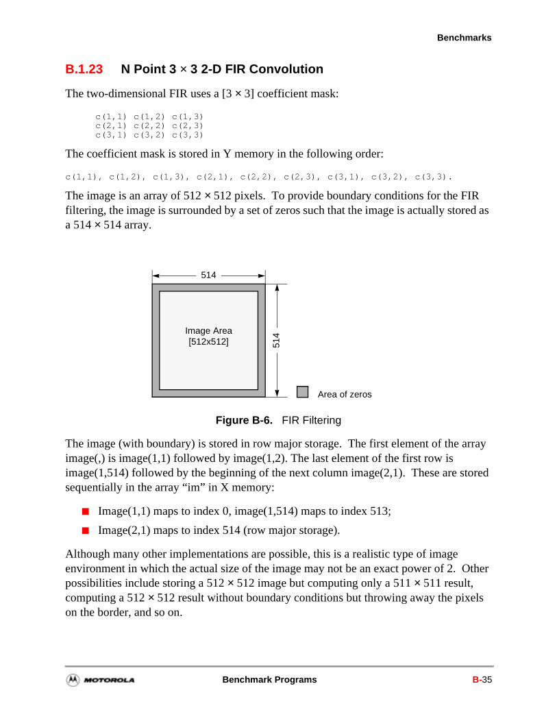
Benchmarks
Other
ls
B.1.23 N Point 3 × 3 2-D FIR Convolution
The two-dimensional FIR uses a [3 × 3] coefficient mask:
c(1,1) c(1,2) c(1,3) c(2,1) c(2,2) c(2,3) c(3,1) c(3,2) c(3,3)
The coefficient mask is stored in Y memory in the following order:
c(1,1), c(1,2), c(1,3), c(2,1), c(2,2), c(2,3), c(3,1), c(3,2), c(3,3).
The image is an array of 512 × 512 pixels. To provide boundary conditions for the FIR filtering, the image is surrounded by a set of zeros such that the image is actually stored as a 514 × 514 array.
The image (with boundary) is stored in row major storage. The first element of the array image(,) is image(1,1) followed by image(1,2). The last element of the first row is image(1,514) followed by the beginning of the next column image(2,1). These are stored sequentially in the array “im” in X memory:
Image(1,1) maps to index 0, image(1,514) maps to index 513;
Image(2,1) maps to index 514 (row major storage).
Although many other implementations are possible, this is a realistic type of image environment in which the actual size of the image may not be an exact power of 2. possibilities include storing a 512 × 512 image but computing only a 511 × 511 result, computing a 512 × 512 result without boundary conditions but throwing away the pixeon the border, and so on.
Figure B-6. FIR Filtering
Image Area[512x512] 51
4
Area of zeros
514
Benchmark Programs B-35
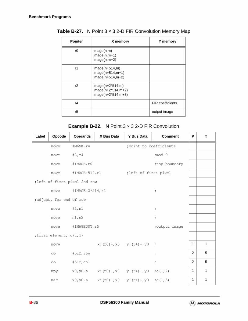
Benchmark Programs
Table B-27. N Point 3 × 3 2-D FIR Convolution Memory Map
Pointer X memory Y memory
r0 image(n,m)image(n,m+1)image(n,m+2)
r1 image(n+514,m)image(n+514,m+1)image(n+514,m+2)
r2 image(n+2*514,m)image(n+2*514,m+2)image(n+2*514,m+3)
r4 FIR coefficients
r5 output image
Example B-22. N Point 3 × 3 2-D FIR Convolution
Label Opcode Operands X Bus Data Y Bus Data Comment P T
move #MASK,r4 ;point to coefficients
move #8,m4 ;mod 9
move #IMAGE,r0 ;top boundary
move #IMAGE+514,r1 ;left of first pixel
;left of first pixel 2nd row
move #IMAGE+2*514,r2 ;
;adjust. for end of row
move #2,n1 ;
move n1,n2 ;
move #IMAGEOUT,r5 ;output image
;first element, c(1,1)
move x:(r0)+,x0 y:(r4)+,y0 ; 1 1
do #512,row ; 2 5
do #512,col ; 2 5
mpy x0,y0,a x:(r0)+,x0 y:(r4)+,y0 ;c(1,2) 1 1
mac x0,y0,a x:(r0)-,x0 y:(r4)+,y0 ;c(1,3) 1 1
B-36 DSP56300 Family Manual
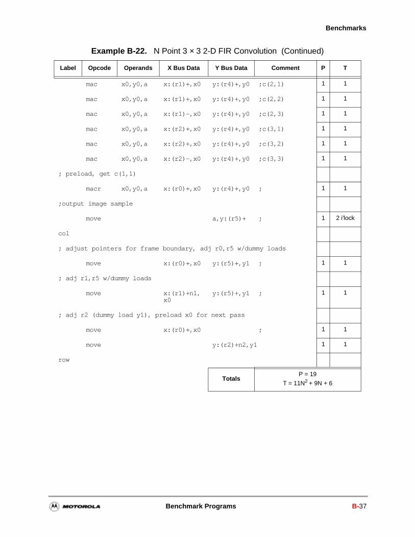
Benchmarks
Label Opcode Operands X Bus Data Y Bus Data Comment P T
mac x0,y0,a x:(r1)+,x0 y:(r4)+,y0 ;c(2,1) 1 1
mac x0,y0,a x:(r1)+,x0 y:(r4)+,y0 ;c(2,2) 1 1
mac x0,y0,a x:(r1)-,x0 y:(r4)+,y0 ;c(2,3) 1 1
mac x0,y0,a x:(r2)+,x0 y:(r4)+,y0 ;c(3,1) 1 1
mac x0,y0,a x:(r2)+,x0 y:(r4)+,y0 ;c(3,2) 1 1
mac x0,y0,a x:(r2)-,x0 y:(r4)+,y0 ;c(3,3) 1 1
; preload, get c(1,1)
macr x0,y0,a x:(r0)+,x0 y:(r4)+,y0 ; 1 1
;output image sample
move a,y:(r5)+ ; 1 2 i’lock
col
; adjust pointers for frame boundary, adj r0,r5 w/dummy loads
move x:(r0)+,x0 y:(r5)+,y1 ; 1 1
; adj r1,r5 w/dummy loads
move x:(r1)+n1,x0
y:(r5)+,y1 ; 1 1
; adj r2 (dummy load y1), preload x0 for next pass
move x:(r0)+,x0 ; 1 1
move y:(r2)+n2,y1 1 1
row
TotalsP = 19
T = 11N2 + 9N + 6
Example B-22. N Point 3 × 3 2-D FIR Convolution (Continued)
Benchmark Programs B-37
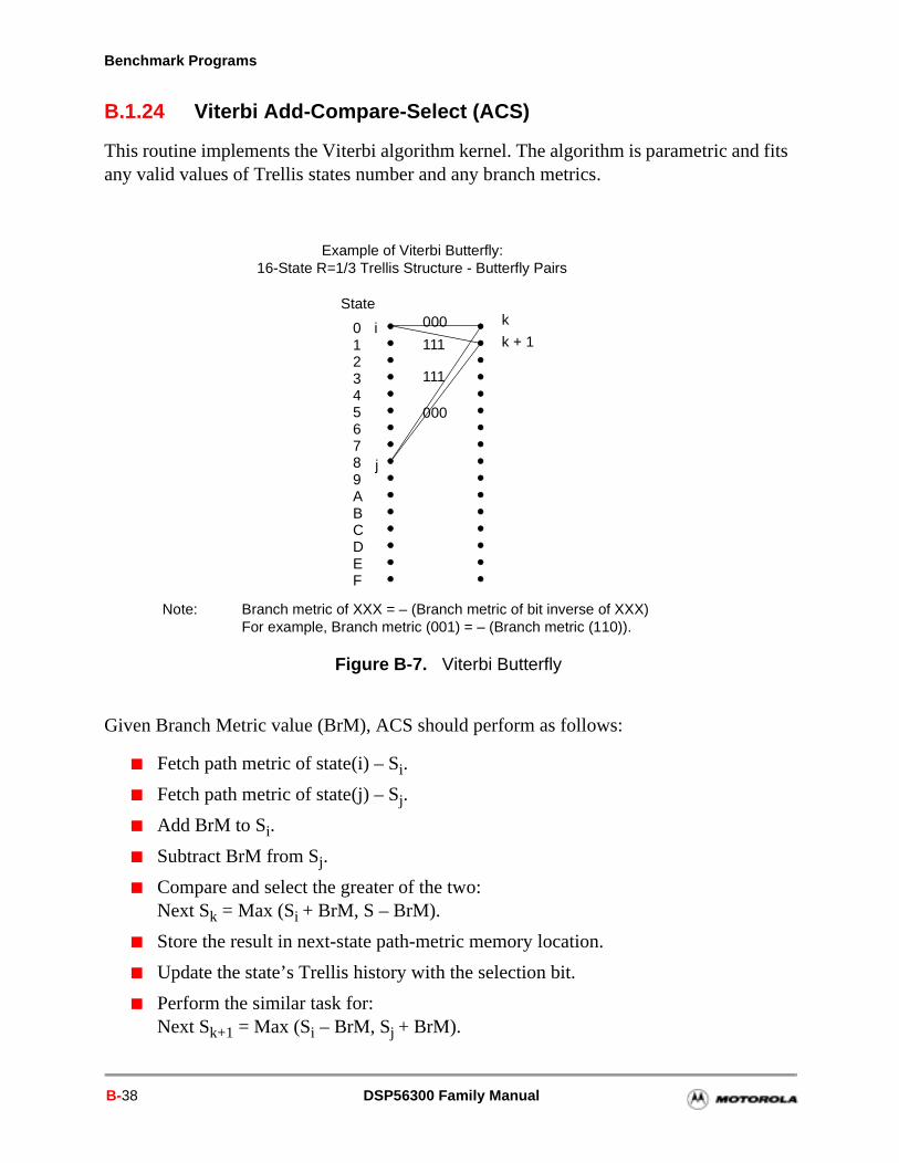
Benchmark Programs
B.1.24 Viterbi Add-Compare-Select (ACS)
This routine implements the Viterbi algorithm kernel. The algorithm is parametric and fits any valid values of Trellis states number and any branch metrics.
Given Branch Metric value (BrM), ACS should perform as follows:
Fetch path metric of state(i) – Si.
Fetch path metric of state(j) – Sj.
Add BrM to Si.
Subtract BrM from Sj.
Compare and select the greater of the two:Next Sk = Max (Si + BrM, S – BrM).
Store the result in next-state path-metric memory location.
Update the state’s Trellis history with the selection bit.
Perform the similar task for: Next Sk+1 = Max (Si – BrM, Sj + BrM).
Figure B-7. Viterbi Butterfly
Example of Viterbi Butterfly:
0123456789ABCDEF
000
111
000
111
State
Note: Branch metric of XXX = – (Branch metric of bit inverse of XXX) For example, Branch metric (001) = – (Branch metric (110)).
16-State R=1/3 Trellis Structure - Butterfly Pairs
i
j
k
k + 1
B-38 DSP56300 Family Manual
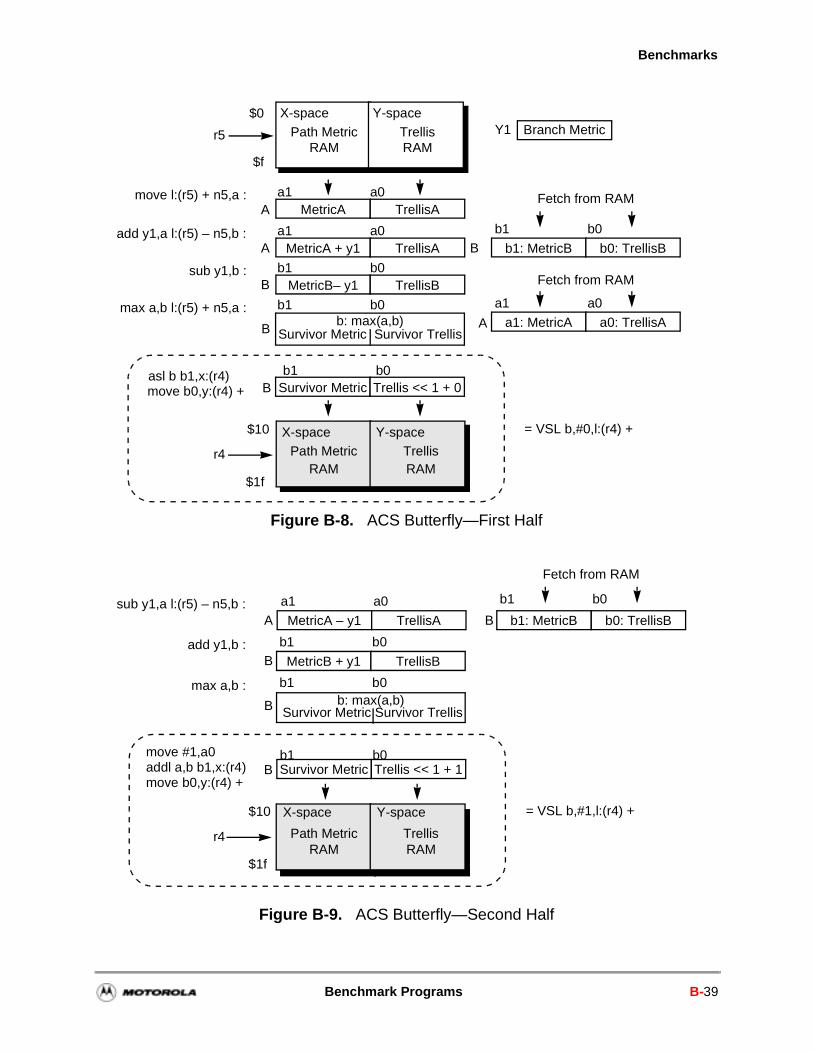
Benchmarks
Figure B-8. ACS Butterfly—First Half
Figure B-9. ACS Butterfly—Second Half
Path MetricRAM
MetricA TrellisA
TrellisRAM
b1: MetricB b0: TrellisB
move l:(r5) + n5,a :
add y1,a l:(r5) – n5,b :MetricA + y1 TrellisA
sub y1,b :MetricB– y1 TrellisB
max a,b l:(r5) + n5,a :b: max(a,b)
Survivor Metrica1: MetricA a0: TrellisA
asl b b1,x:(r4)move b0,y:(r4) + Survivor Metric Trellis << 1 + 0
b0b1
b0b1
b0b1
a0a1
a0a1
r5
Path MetricRAM
TrellisRAM
r4
= VSL b,#0,l:(r4) +
Fetch from RAM
Fetch from RAM
Branch Metric
b0b1
a0a1
A
A
B
B A
B
Y1$0
$f
X-space Y-space
X-space Y-space$10
$1f
B
Survivor Trellis
Survivor Metric Trellis << 1 + 1b0b1
Path MetricRAM
TrellisRAM
r4
= VSL b,#1,l:(r4) +
move #1,a0addl a,b b1,x:(r4)move b0,y:(r4) +
X-space Y-space$10
$1f
B
b1: MetricB b0: TrellisBsub y1,a l:(r5) – n5,b :
MetricA – y1 TrellisA
add y1,b :MetricB + y1 TrellisB
max a,b :b: max(a,b)
Survivor Metric
b0b1
b0b1
a0a1
Fetch from RAM
b0b1
A
B
B
B
Survivor Trellis
Benchmark Programs B-39
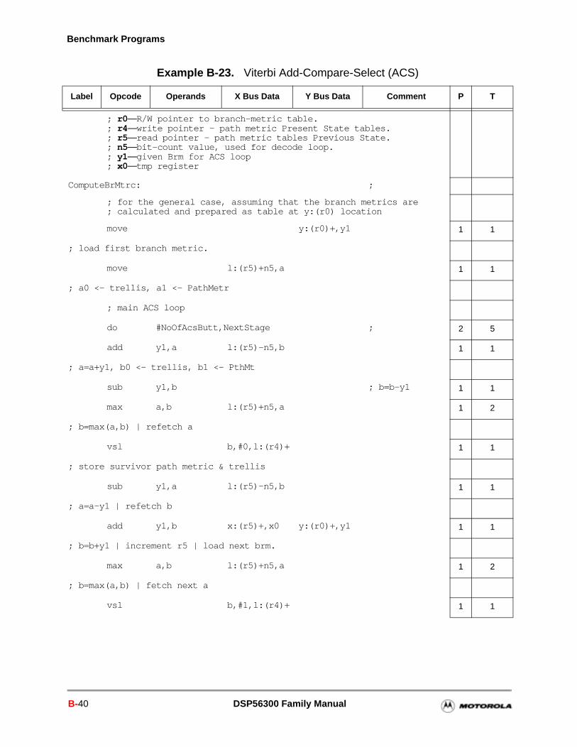
Benchmark Programs
Example B-23. Viterbi Add-Compare-Select (ACS)
Label Opcode Operands X Bus Data Y Bus Data Comment P T
; r0—R/W pointer to branch-metric table.; r4—write pointer - path metric Present State tables.; r5—read pointer - path metric tables Previous State.; n5—bit-count value, used for decode loop.; y1—given Brm for ACS loop; x0—tmp register
ComputeBrMtrc: ;
; for the general case, assuming that the branch metrics are; calculated and prepared as table at y:(r0) location
move y:(r0)+,y1 1 1
; load first branch metric.
move l:(r5)+n5,a 1 1
; a0 <- trellis, a1 <- PathMetr
; main ACS loop
do #NoOfAcsButt,NextStage ; 2 5
add y1,a l:(r5)-n5,b 1 1
; a=a+y1, b0 <- trellis, b1 <- PthMt
sub y1,b ; b=b-y1 1 1
max a,b l:(r5)+n5,a 1 2
; b=max(a,b) | refetch a
vsl b,#0,l:(r4)+ 1 1
; store survivor path metric & trellis
sub y1,a l:(r5)-n5,b 1 1
; a=a-y1 | refetch b
add y1,b x:(r5)+,x0 y:(r0)+,y1 1 1
; b=b+y1 | increment r5 | load next brm.
max a,b l:(r5)+n5,a 1 2
; b=max(a,b) | fetch next a
vsl b,#1,l:(r4)+ 1 1
B-40 DSP56300 Family Manual
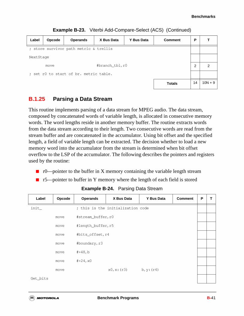
Benchmarks
B.1.25 Parsing a Data Stream
This routine implements parsing of a data stream for MPEG audio. The data stream, composed by concatenated words of variable length, is allocated in consecutive memory words. The word lengths reside in another memory buffer. The routine extracts words from the data stream according to their length. Two consecutive words are read from the stream buffer and are concatenated in the accumulator. Using bit offset and the specified length, a field of variable length can be extracted. The decision whether to load a new memory word into the accumulator from the stream is determined when bit offset overflow to the LSP of the accumulator. The following describes the pointers and registers used by the routine:
r0—pointer to the buffer in X memory containing the variable length stream
r5—pointer to buffer in Y memory where the length of each field is stored
Label Opcode Operands X Bus Data Y Bus Data Comment P T
; store survivor path metric & trellis
NextStage
move #branch_tbl,r0 2 2
; set r0 to start of br. metric table.
Totals 14 10N + 9
Example B-24. Parsing Data Stream
Label Opcode Operands X Bus Data Y Bus Data Comment P T
init_ ; this is the initialization code
move #stream_buffer,r0
move #length_buffer,r5
move #bits_offset,r4
move #boundary,r3
move #>48,b
move #>24,x0
move x0,x:(r3) b,y:(r4)
Get_bits
Example B-23. Viterbi Add-Compare-Select (ACS) (Continued)
Benchmark Programs B-41
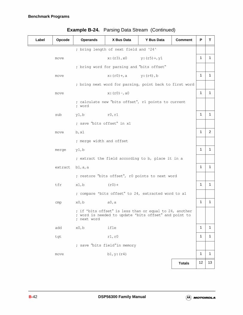
Benchmark Programs
Label Opcode Operands X Bus Data Y Bus Data Comment P T
; bring length of next field and ‘24‘
move x:(r3),x0 y:(r5)+,y1 1 1
; bring word for parsing and "bits offset "
move x:(r0)+,a y:(r4),b 1 1
; bring next word for parsing, point back to first word
move x:(r0)-,a0 1 1
; calculate new "bits offset ", r1 points to current; word
sub y1,b r0,r1 1 1
; save "bits offset " in x1
move b,x1 1 2
; merge width and offset
merge y1,b 1 1
; extract the field according to b, place it in a
extract b1,a,a 1 1
; restore "bits offset ", r0 points to next word
tfr x1,b (r0)+ 1 1
; compare "bits offset " to 24, extracted word to a1
cmp x0,b a0,a 1 1
; if "bits offset " is less than or equal to 24, another ; word is needed to update "bits offset " and point to ; next word
add x0,b ifle 1 1
tgt r1,r0 1 1
; save "bits field " in memory
move b1,y:(r4) 1 1
Totals 12 13
Example B-24. Parsing Data Stream (Continued)
B-42 DSP56300 Family Manual
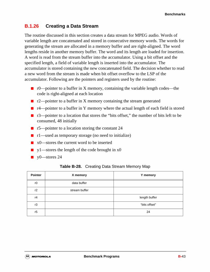
Benchmarks
red
be
B.1.26 Creating a Data Stream
The routine discussed in this section creates a data stream for MPEG audio. Words of variable length are concatenated and stored in consecutive memory words. The words for generating the stream are allocated in a memory buffer and are right-aligned. The word lengths reside in another memory buffer. The word and its length are loaded for insertion. A word is read from the stream buffer into the accumulator. Using a bit offset and the specified length, a field of variable length is inserted into the accumulator. The accumulator is stored containing the new concatenated field. The decision whether to read a new word from the stream is made when bit offset overflow to the LSP of the accumulator. Following are the pointers and registers used by the routine:
r0—pointer to a buffer in X memory, containing the variable length codes—thecode is right-aligned at each location
r2—pointer to a buffer in X memory containing the stream generated
r4—pointer to a buffer in Y memory where the actual length of each field is sto
r3—pointer to a location that stores the “bits offset,” the number of bits left to consumed, 48 initially
r5—pointer to a location storing the constant 24
r1—used as temporary storage (no need to initialize)
x0—stores the current word to be inserted
y1—stores the length of the code brought in x0
y0—stores 24
Table B-28. Creating Data Stream Memory Map
Pointer X memory Y memory
r0 data buffer
r2 stream buffer
r4 length buffer
r3 “bits offset”
r5 24
Benchmark Programs B-43
Benchmark Programs
Example B-25. Creating Data Stream
Label Opcode Operands X Bus Data Y Bus Data Comment P T
init_ ;this is the initialization code
move #data_buffer,r0
move #stream_buffer,r2
move #length_buffer,r4
move #bits_offset,r3
move #boundary,r5
move #>48,b
move #>24,y0
move b,x:(r3) y0,y:(r5)
Put_bits
; bring code and its length
move x:(r0)+,x0 y:(r4)+,y1 1 1
; bring "bits offset" and ‘24‘
move x:(r3),b y:(r5),y0 1 1
; calculate new "bits offset", bring current word ; from stream buffer
sub y1,b x:(r2),a 1 1
; save "bits offset" in x1
move b,x1 1 2
; merge width and offset
merge y1,b 1 1
; insert the field according to b, place it in a
insert b1,x0,a 1 1
; restore "bits offset", r1 points to current word
tfr x1,b r2,r1 1 1
; compare "bits offset" to 24, send new word to stream; buffer
cmp y0,b a1,x:(r2)+ 1 1
B-44 DSP56300 Family Manual
Benchmarks
B.1.27 Parsing a Hoffman Code Data Stream
The routine discussed in this section parses a Hoffman code data stream. It extracts a bit field from the stream and brings two consecutive words to the accumulator from the stream buffer. An address word is extracted using a bit offset and a field length. The field length is determined by the number of bits needed by the address of the two Hoffman code lookup tables. A word is loaded from the first lookup table. If the "Hit" bit in the word is not set, then a field of variable length is extracted. The length of the extracted field is specified in the length field in the word. The bit offset is updated according to the length of the extracted word. If the "Hit" bit in the word is set, a new address word is read from the stream. A word is brought from the second lookup table. The bit field is extracted according to the same guidelines.
Label Opcode Operands X Bus Data Y Bus Data Comment P T
; send a0 to next location in stream buffer in case of ; crossing boundary
move a0,x:(r2) 1 2
; if "bits offset" is less than or equal to 24, then ; update "bits offset" and point to the next word ; in stream buffer
add y0,b ifle 1 1
tgt r1,r2 1 1
; save "bits offset" in memory
move b1,y:(r4) 1 1
Totals 12 14
Example B-25. Creating Data Stream (Continued)
Benchmark Programs B-45
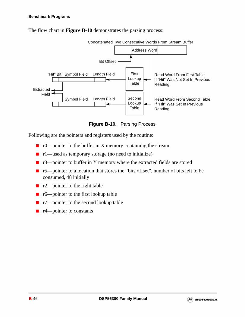
Benchmark Programs
The flow chart in Figure B-10 demonstrates the parsing process:
Following are the pointers and registers used by the routine:
r0—pointer to the buffer in X memory containing the stream
r1—used as temporary storage (no need to initialize)
r3—pointer to buffer in Y memory where the extracted fields are stored
r5—pointer to a location that stores the “bits offset”, number of bits left to be consumed, 48 initially
r2—pointer to the right table
r6—pointer to the first lookup table
r7—pointer to the second lookup table
r4—pointer to constants
Figure B-10. Parsing Process
Concatenated Two Consecutive Words From Stream Buffer
FirstLookupTable
SecondLookupTable
Address Word
Bit Offset
Symbol Field Length Field"Hit" Bit
Symbol Field Length Field
ExtractedField
Read Word From First TableIf "Hit" Was Not Set In Previous Reading
Read Word From Second TableIf "Hit" Was Set In Previous Reading
B-46 DSP56300 Family Manual
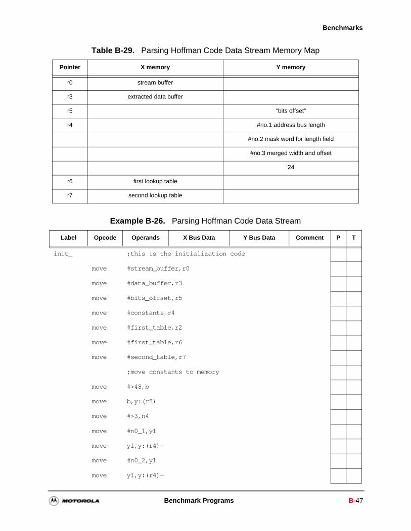
Benchmarks
Table B-29. Parsing Hoffman Code Data Stream Memory Map
Pointer X memory Y memory
r0 stream buffer
r3 extracted data buffer
r5 “bits offset”
r4 #no.1 address bus length
#no.2 mask word for length field
#no.3 merged width and offset
‘24‘
r6 first lookup table
r7 second lookup table
Example B-26. Parsing Hoffman Code Data Stream
Label Opcode Operands X Bus Data Y Bus Data Comment P T
init_ ;this is the initialization code
move #stream_buffer,r0
move #data_buffer,r3
move #bits_offset,r5
move #constants,r4
move #first_table,r2
move #first_table,r6
move #second_table,r7
;move constants to memory
move #>48,b
move b,y:(r5)
move #>3,n4
move #n0_1,y1
move y1,y:(r4)+
move #n0_2,y1
move y1,y:(r4)+
Benchmark Programs B-47
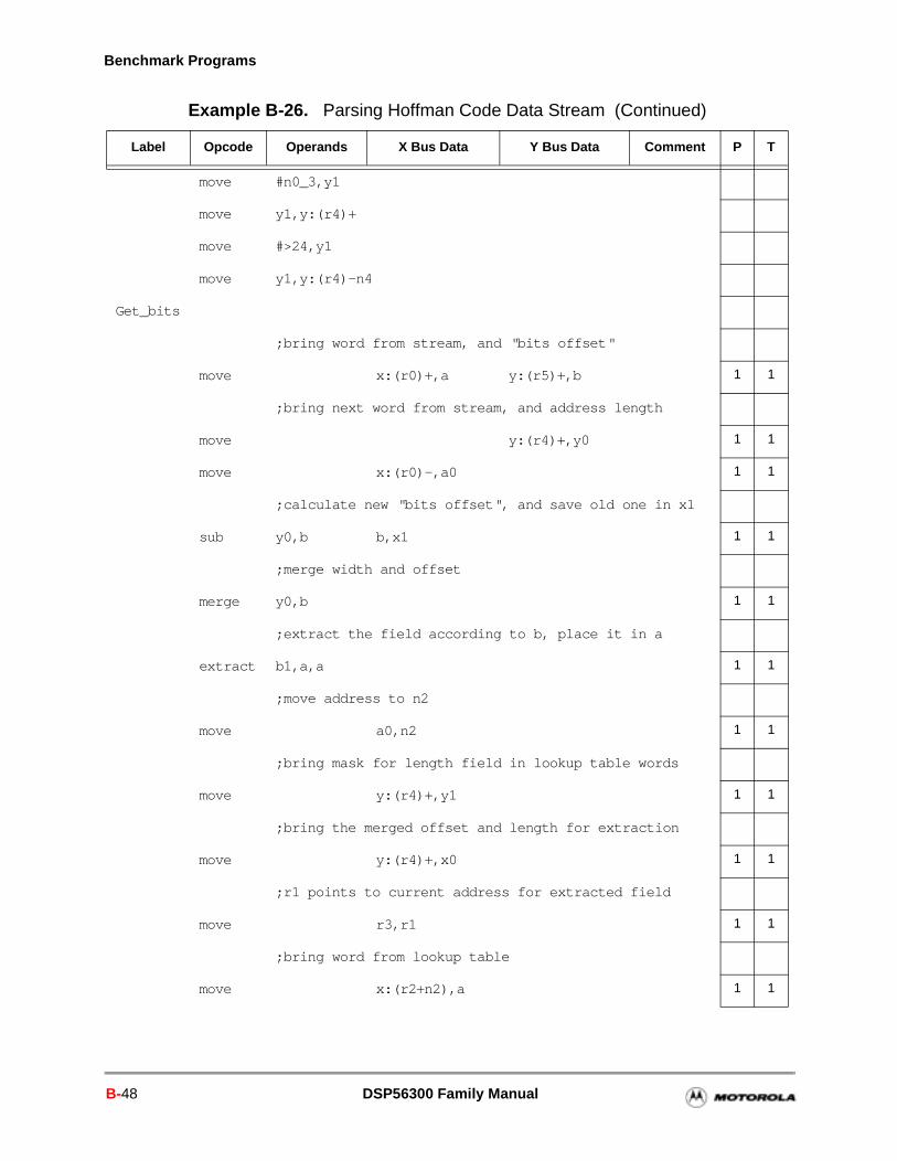
Benchmark Programs
Label Opcode Operands X Bus Data Y Bus Data Comment P T
move #n0_3,y1
move y1,y:(r4)+
move #>24,y1
move y1,y:(r4)-n4
Get_bits
;bring word from stream, and "bits offset"
move x:(r0)+,a y:(r5)+,b 1 1
;bring next word from stream, and address length
move y:(r4)+,y0 1 1
move x:(r0)-,a0 1 1
;calculate new "bits offset", and save old one in x1
sub y0,b b,x1 1 1
;merge width and offset
merge y0,b 1 1
;extract the field according to b, place it in a
extract b1,a,a 1 1
;move address to n2
move a0,n2 1 1
;bring mask for length field in lookup table words
move y:(r4)+,y1 1 1
;bring the merged offset and length for extraction
move y:(r4)+,x0 1 1
;r1 points to current address for extracted field
move r3,r1 1 1
;bring word from lookup table
move x:(r2+n2),a 1 1
Example B-26. Parsing Hoffman Code Data Stream (Continued)
B-48 DSP56300 Family Manual
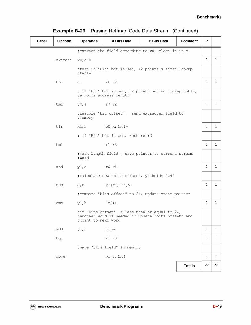
Benchmarks
Label Opcode Operands X Bus Data Y Bus Data Comment P T
;extract the field according to x0, place it in b
extract x0,a,b 1 1
;test if "Hit" bit is set, r2 points s first lookup;table
tst a r6,r2 1 1
; if "Hit" bit is set, r2 points second lookup table,;a holds address length
tmi y0,a r7,r2 1 1
;restore "bit offset" , send extracted field to;memory
tfr x1,b b0,x:(r3)+ 1 1
; if "Hit" bit is set, restore r3
tmi r1,r3 1 1
;mask length field , save pointer to current stream;word
and y1,a r0,r1 1 1
;calculate new "bits offset", y1 holds ’24’
sub a,b y:(r4)-n4,y1 1 1
;compare "bits offset" to 24, update steam pointer
cmp y1,b (r0)+ 1 1
;if "bits offset" is less than or equal to 24,;another word is needed to update "bits offset" and ;point to next word
add y1,b ifle 1 1
tgt r1,r0 1 1
;save "bits field" in memory
move b1,y:(r5) 1 1
Totals 22 22
Example B-26. Parsing Hoffman Code Data Stream (Continued)
Benchmark Programs B-49

Benchmark Programs
B-50 DSP56300 Family Manual
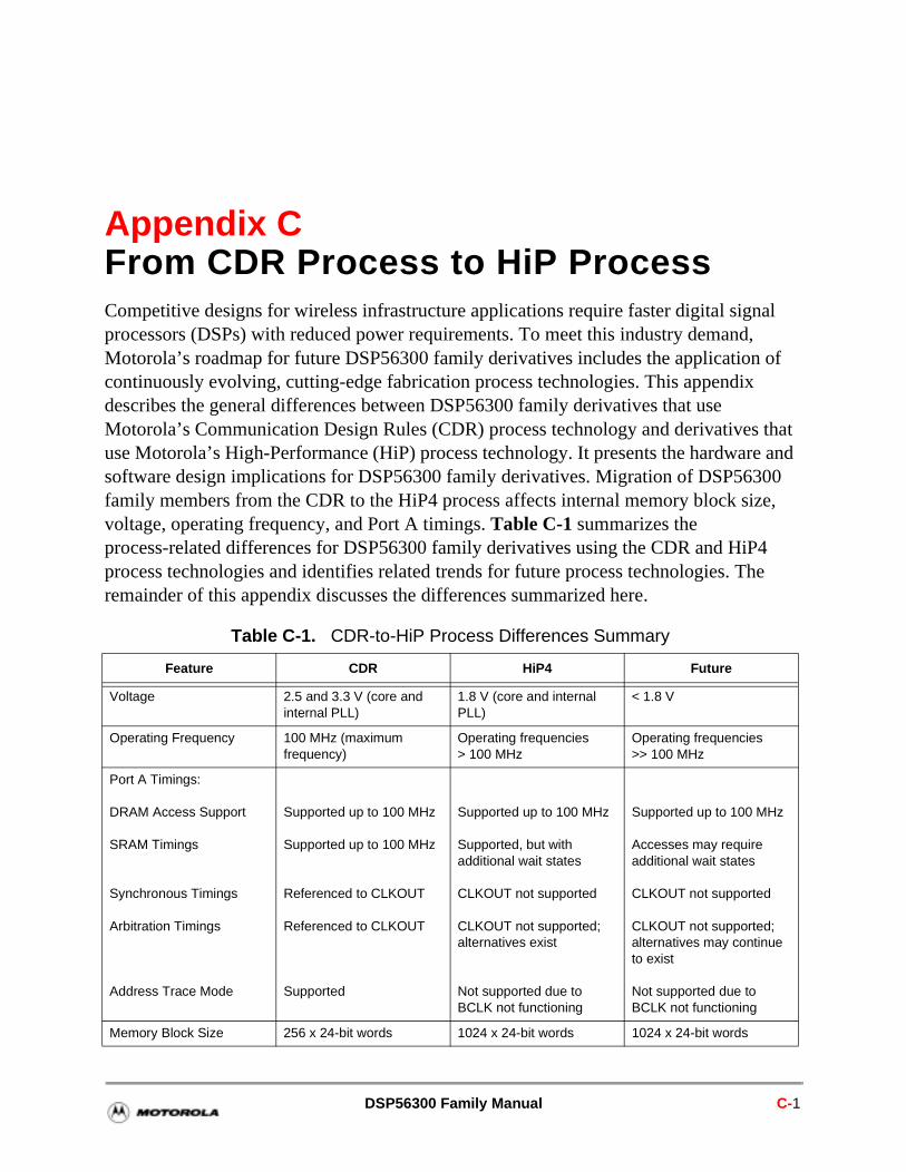
of
that e and 00 e,
4 he
Appendix CFrom CDR Process to HiP ProcessCompetitive designs for wireless infrastructure applications require faster digital signal processors (DSPs) with reduced power requirements. To meet this industry demand, Motorola’s roadmap for future DSP56300 family derivatives includes the applicationcontinuously evolving, cutting-edge fabrication process technologies. This appendixdescribes the general differences between DSP56300 family derivatives that use Motorola’s Communication Design Rules (CDR) process technology and derivativesuse Motorola’s High-Performance (HiP) process technology. It presents the hardwarsoftware design implications for DSP56300 family derivatives. Migration of DSP563family members from the CDR to the HiP4 process affects internal memory block sizvoltage, operating frequency, and Port A timings. Table C-1 summarizes the process-related differences for DSP56300 family derivatives using the CDR and HiPprocess technologies and identifies related trends for future process technologies. Tremainder of this appendix discusses the differences summarized here.
Table C-1. CDR-to-HiP Process Differences Summary
Feature CDR HiP4 Future
Voltage 2.5 and 3.3 V (core and internal PLL)
1.8 V (core and internal PLL)
< 1.8 V
Operating Frequency 100 MHz (maximum frequency)
Operating frequencies > 100 MHz
Operating frequencies >> 100 MHz
Port A Timings:
DRAM Access Support
SRAM Timings
Synchronous Timings
Arbitration Timings
Address Trace Mode
Supported up to 100 MHz
Supported up to 100 MHz
Referenced to CLKOUT
Referenced to CLKOUT
Supported
Supported up to 100 MHz
Supported, but with additional wait states
CLKOUT not supported
CLKOUT not supported; alternatives exist
Not supported due to BCLK not functioning
Supported up to 100 MHz
Accesses may require additional wait states
CLKOUT not supported
CLKOUT not supported; alternatives may continue to exist
Not supported due to BCLK not functioning
Memory Block Size 256 x 24-bit words 1024 x 24-bit words 1024 x 24-bit words
DSP56300 Family Manual C-1
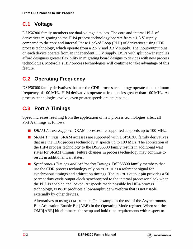
From CDR Process to HiP Process
f this
imum z. As
ll
z.
es on of t to
hen
s e
C.1 Voltage
DSP56300 family members are dual-voltage devices. The core and internal PLL of derivatives migrating to the HiP4 process technology operate from a 1.8 V supply compared to the core and internal Phase Locked Loop (PLL) of derivatives using CDR process technology, which operate from a 2.5 V and 3.3 V supply. The input/output pins on each device operate from an independent 3.3 V supply. DSPs with split power supplies afford designers greater flexibility in migrating board designs to devices with new process technologies. Motorola’s HiP process technologies will continue to take advantage ofeature.
C.2 Operating Frequency
DSP56300 family derivatives that use the CDR process technology operate at a maxfrequency of 100 MHz. HiP4 derivatives operate at frequencies greater than 100 MHprocess technologies evolve, even greater speeds are anticipated.
C.3 Port A Timings
Speed increases resulting from the application of new process technologies affect aPort A timings as follows:
DRAM Access Support. DRAM accesses are supported at speeds up to 100 MH
SRAM Timings. SRAM accesses are supported with DSP56300 family derivativthat use the CDR process technology at speeds up to 100 MHz. The applicatithe HiP4 process technology to the DSP56300 family results in additional waistates for SRAM timings. Future changes in process technology may continueresult in additional wait states.
Synchronous Timings and Arbitration Timings. DSP56300 family members that use the CDR process technology rely on CLKOUT as a reference signal for synchronous timings and arbitration timings. The CLKOUT output pin provides a 50percent duty cycle output clock synchronized to the internal processor clock wthe PLL is enabled and locked. At speeds made possible by HiP4 process technology, CLKOUT produces a low-amplitude waveform that is not usable externally by other devices.
Alternatives to using CLKOUT exist. One example is the use of the AsynchronouBus Arbitration Enable Bit (ABE) in the Operating Mode register. When set, thOMR[ABE] bit eliminates the setup and hold time requirements with respect to
C-2 DSP56300 Family Manual
Memory Block Size
CLKOUT for BB and BG. Future changes in process technology may continue to produce alternatives to CLKOUT.
Address Trace Mode. Address Trace mode, when available and enabled by setting the ATE bit in the Operating Mode Register of DSP56300 family derivatives that use the CDR process technology, allows users to determine the address of internal memory accesses. Specifically, when the OMR[ATE] bit is set, BCLK serves as a sampling signal and results in output of the memory access address on the address lines. With the application of HiP4 process technology, BCLK does not function. Without BCLK functioning, no signal exists to initiate the sampling process, and the DSP does not output any addresses. Therefore, Address Trace mode is not supported under the HiP4 process.
C.4 Memory Block Size
The internal memory block size of DSP56300 derivatives using the HiP4 process technology is 1024 x 24-bit words compared to 256 x 24-bit words in CDR derivatives. This change in size affects DMA/core contention (and EFCOP/core contention for derivatives, such as the DSP56307, that have an enhanced filter coprocessor).
In CDR derivatives, the internal RAM is divided into 256-word blocks. A situation of contention exists if the core and DMA access the same block of 256 words. If both the core and DMA access the same block, then the core always has priority, and the DMA is delayed until a free slot is available. If the core and DMA access different blocks, they do not interfere with one another; each continues to operate at its maximum speed. Memory block boundaries are located at 256 word addresses.
This same situation applies to HiP4 derivatives, except that contention exists if the core and DMA access the same block of 1024 words. Memory block boundaries are located at 1 K words addresses. To avoid DMA/core contention, DMA and core accesses must address different 1024-word blocks. Figure C-1 shows two examples of core and DMA accesses to different 256-word blocks in the DSP56307 (no contention) and the resulting effect of these same accesses in a hypothetical HiP4 derivative.
From CDR Process to HiP Process C-3
From CDR Process to HiP Process
The same change in block size applies to EFCOP/core contention in derivatives that contain an EFCOP. Unlike Core/DMA contention, EFCOP/core contention may result in faulty data output in the Filter Data Output Register. For example, in the DSP56307, contention occurs if the EFCOP and core attempt to access the same 256 word block. In HiP4 derivatives, contention occurs if the EFCOP and core attempt to access the same 1 K words block. Both the DSP56307 and future HiP4 derivatives include the Data/Coefficient Transfer Contention (FCONT) bit in the EFCOP Control Status Register. The FCONT bit allows programmers to detect when EFCOP/core contention occurs.
256 1024
256
256
256
256 1024
256
Example 1: 256 Example 1:
No contention
Core Access → 256 No contention
Core Access →
DMA Access → 256 DMA Access → 1024
Example 2: 256 Example 2:
No contention
DMA Access → 256Contention
DMA Access →
Core Access → 256 Core Access →
CDR Derivatives HiP4 Derivatives
Figure C-1. CDR/HiP DMA and Core Access Comparisons
C-4 DSP56300 Family Manual
Index
A
AAR. See Address Attribute Registers (AARs)ABS instruction 12-7, 13-5accumulator extension register 3-17accumulator registers (A or B) 3-4accumulator shifter 3-5ADC instruction 12-7, 13-6ADD instruction 12-8, 13-8adder
modulo 1-4offset 1-4reverse-carry 1-4
ADDL instruction 12-8, 13-9ADDR instruction 12-8, 13-10Address Attribute Registers (AARs) 9-15
Bit Definitions 9-16Bus Access Type (BAT) bit 9-18Bus Address Attribute Polarity (BAAP) bit 9-18Bus Address Multiplexing (BAM) bit 9-17Bus Address to Compare (BAC) bit 9-16Bus Number of Address Bits to Compare (BNC)
bit 9-16Bus Packing Enable (BPAC) bit 9-17Bus Program Memory Enable (BPEN) bit 9-18Bus X Data Memory Enable (BXEN) bit 9-18Bus Y Data Memory Enable (BYEN) bit 9-17
Address Generation Unit (AGU) 1-3, 4-1addressing modes 4-6
PC-Relative mode 4-6, 4-9Register Direct mode 4-6, 4-7Register Indirect mode 4-6, 4-7Special Address mode 4-9special address modes 4-6
Address modification 4-11, 4-12address modifier types
Linear addressing 4-10Modulo addressing 4-11Multiple wrap-around modulo addressing 4-11Reverse-carry addressing 4-10
address register interlock A-11address registers 4-5
increment or decrement 4-5Address Trace Mode 5-8, 7-1addressing modes 4-6
PC Relative mode 4-9Register Direct mode 4-7Register Indirect mode 4-7
DSP56300 Fa
Special Address mode 4-9AGU. See Address Generation Unitalgorithms, evaluating and increasing their speed 5-7analog signal processing 1-8analog-to-digital 1-9AND instruction 12-10, 13-11ANDI instruction 3-13, 5-11, 12-10, 13-13arithmetic computations 5-11arithmetic instructions 12-7
Absolute Value (ABS) 12-7, 13-5Add (ADD) 12-8, 13-8Add Long With Carry (ADC) 12-7, 13-6Arithmetic Shift Left (ASL) 12-8, 13-14Arithmetic Shift Right (ASR) 12-8, 13-16Clear an Operand (CLR) 12-8, 13-45Compare (CMP) 12-8, 13-46Compare Magnitude (CMPM) 12-8, 13-48Compare Unsigned (CMPU) 12-8, 13-49Decrement Accumulator (DEC) 12-8, 13-52Divide Iteration (DIV) 12-8, 13-53Double Precision Multiply-Accumulate
(DMAC) 12-8, 13-56Fast Accumulator Normalize (NORMF) 12-9,
13-147-13-148Increment Accumulator (INC) 12-8, 13-77Mixed Multiply (MPY(su,uu)) 12-9, 13-139Mixed Multiply-Accumulate (MAC(su,uu)) 12-8,
13-102Negate Accumulator (NEG) 12-9, 13-144Round (RND) 12-9, 13-163-13-164Shift Left and ADD (ADDL) 12-8, 13-9Shift Left and Subtract (SUBL) 12-9, 13-174Shift Right and Add (ADDR) 12-8, 13-10Shift Right and Subtract (SUBR) 12-9, 13-175Signed MAC and Round With Immediate Operand
(MACRI) 13-105Signed Multiply (MPY) 12-9, 13-137-13-138Signed Multiply Accumulate (MAC) 12-8,
13-99-13-100Signed Multiply Accumulate and Round
(MACR) 12-8, 13-103-13-104Signed Multiply Accumulate and Round With
Immediate Operand) (MACRI) 12-8Signed Multiply Accumulate With Immediate
Operand (MACI) 12-8, 13-101Signed Multiply and Round (MPYR) 12-9,
13-141-13-142
mily Manual Index-1
Signed Multiply and Round With Immediate Operand (MPYRI) 12-9, 13-143
Signed Multiply With Immediate Operand (MPYI) 12-9, 13-140
Subtract (SUB) 12-9, 13-172-13-173Subtract Long With Carry (SBC) 12-9, 13-169Test Accumulator (TST) 13-181Test an Operand (TST) 12-9Transfer by Magnitude (MAXM) 12-8, 13-107Transfer by Signed Value (MAX) 12-8, 13-106Transfer Conditionally (Tcc) 12-9, 13-176-13-177Transfer Data ALU Register (TFR) 12-9, 13-178
arithmetic overflow 5-18arithmetic saturation 3-4, 3-11Arithmetic Saturation Mode (SM). See PCU
configuration and status registers, Status Register (SR)
arithmetic stall 3-21arithmetic unit 3-20ASL instruction 12-8, 13-14ASR instruction 12-8, 13-16ATE (Address Trace Enable) bit of the OMR 5-8
B
barrel shifter 1-2, 3-3Bcc instruction 12-13, 13-18BCHG instruction 3-20, 9-12, 12-11, 13-19-13-20BCLR instruction 3-20, 9-12, 12-11, 13-22-13-23BCR. See Bus Control Register (BCR)benchmark programs B-1bit manipulation instructions 3-22, 12-11
Bit Test (BTST) 12-11, 13-41Bit Test and Change (BCHG) 12-11, 13-19-13-20Bit Test and Clear (BCLR) 12-11, 13-22-13-23Bit Test and Set (BSET) 9-12, 12-11
bit parsing instructions 3-20block diagram
Address Generation Unit (AGU) 4-2Clock Generator 6-5Data ALU 3-2DSP56300 family core blocks 2-3OnCE module 7-11OnCE Trace Logic 7-22Phase Locked Loop (PLL) 6-2PLL clock generator 6-1Test Access Port (TAP) With OnCE 7-4
Block Floating Point FFT support 3-14Boundary Scan Register (BSR) 7-2, 7-3, 7-5BRA instruction 12-13, 13-25BRCLR instruction 3-20, 13-27BRKcc inside DO loops A-19BRKcc instruction 5-24, 12-11, 13-28BRSET instruction 3-20, 13-29
BScc instruction 12-13, 13-31-13-32BSCLR instruction 3-20, 3-22, 13-33BSET instruction 3-20, 3-22, 9-12, 12-11, 13-35BSR instruction 12-13, 13-38BSR. See Boundary Scan RegisterBSSET instruction 3-20, 13-39BTST instruction 3-20, 12-11, 13-41Burst Enable (BE) bit 8-3bus arbitration examples
Bus Busy 9-14bus lock 9-14bus parking 9-15default 9-14low priority 9-14Normal 9-14
bus arbitration protocol 9-12bus arbitration scheme 9-13bus arbitration signals
Bus Busy (BB) 9-11Bus Grant (BG) 9-11Bus Request (BR 9-11
Bus Control Register (BCR) 9-12, 9-15, 9-19Bit Definitions 9-19Bus Area 0 Wait State Control (BA0W) bit 9-20Bus Area 1 Wait State Control (BA1W) bit 9-20Bus Area 2 Wait State Control (BA2W) bit 9-20Bus Area 3 Wait State Control (BA3W) bit 9-20Bus Default Area Wait State Control (BDFW)
bit 9-19Bus Lock Hold (BLH) bit 9-13, 9-19Bus Request Hold (BRH) bit 9-13, 9-19Bus State (BBS) bit 9-13, 9-19
Bus Interface Unit (BIU) 10-9bus parking 9-13, 9-14bus signals, external 9-2BYPASS (JTAG) instruction 7-10
C
Cache Enable (CE) bit 5-11, 5-13, 8-1, 8-3cache support 7-20Carry (C) bit in the SR 5-18CCR (Condition Code Register). See PCU configuration
and status registersCDR to the HiP4 process C-1CE (Cache Enable) bit. See Cache Enable (CE) bitcharge pump loop filter 6-3Chip Select (CS) signals 9-5circular buffer 4-10, 10-4, 10-13, 10-15CLAMP instruction 7-9CLB instruction 12-10, 13-43CLKGEN. See Clock GeneratorCLKOUT 6-2, 6-4, 6-5, 9-7Clock Generator (CLKGEN) 1-6, 6-1, 6-5
Index-2 DSP56300 Family Manual
clock input frequency division 6-2, 6-4Clock Out Disable (COD) 6-7Clock Output Disable (COD) bit in the PCTL
register 6-2clock synchronization 6-10CLR instruction 12-8, 13-45CMP instruction 12-8, 13-46CMPM instruction 12-8, 13-48CMPU instruction 12-8, 13-49COD (Clock Ouput Disable) bit in the PCTL 6-7COM (Chip Operating Mode) byte of the OMR 5-6Communication Design Rules (CDR) process C-1condition code computation 12-20Condition Code Register (CCR). See PCU configuration
and status registersCondition Codes 12-15conditional branch instruction A-18Control hardware DO loops and REP 5-1convergent rounding (round-to-nearest-even number).
See roundingCore. See DSP56300 family corecounter modes, DMA channel. See DMA counter
modes
D
DALU register A-29Data ALU 3-1, 5-11
input registers 3-3interlock A-11operations 3-7, 5-11programming model 3-15rounding 5-12scaling 3-6source operands 3-2
Data Arithmetic Logic Unit. See Data ALUdata limiters 3-6data representation 3-7data shifter/limiter circuits 3-5data transfer 8-8, 10-6DCR. See DMA Control Registers (DCRs)DCR. See DRAM Control RegisterDebug Event 7-1DEBUG instruction 12-13, 13-50Debug mode in OnCE module 7-23DEBUG_REQUEST instruction 7-10
executing in OnCE module 7-23DEBUGcc instruction 12-13, 13-51debugging interface signals 7-1
Debug Event (DE) 7-2Test Clock (TCK) 7-1Test Data Input (TDI) 7-1Test Data Output (TDO) 7-2Test Mode Select (TMS) 7-1
Test Reset (TRST) 7-2debugging procedures, OnCE examples 7-28debugging tool 5-8debugging, Instruction Cache operation 8-10DEC instruction 12-8, 13-52Decode instructions 5-1dedicated TAP 7-3digital signal processing 1-9digital-to-analog 1-9Direct Memory Access (DMA). See DMADIV instruction 12-8, 13-53Divide Factor (DF) 1-6DMA 1-7
3D modes (D3D = 1) 10-22address generation mode 10-22advantages of using 10-1Bus Interface Unit (BIU) operations 10-9byte packing 10-9channel priority levels 10-7channels 10-2circular buffer 10-4, 10-13Control Registers (DCRs) 10-16
Bit Definitions 10-16DMA Address Mode (DAM) bit 10-20, 10-21DMA Channel Enable (DE) bit 10-16DMA Channel Priority (DPR) bit 10-18DMA Continuous Mode Enable (DCON)
bit 10-19DMA Destination Space (DDS) bit 10-21DMA Interrupt Enable (DIE) bit 10-16DMA Request Source (DRS) bit 10-20DMA Source Space (DSS) bit 10-21DMA Transfer Mode (DTM) bit 10-17Three-Dimensional Mode (D3D) bit 10-20
counter modesCounter (DCO) register 10-2Counter Mode A 10-11Counter Mode B 10-12Counter Modes C, D and E 10-14Counters (DCO) 10-10data structure specification 10-3Dual Counter mode 10-13Single-Counter mode 10-16
DCR. See DMA Control Registers (DCRs)Destination Address Registers (DDRs) 10-2, 10-10DMA Channel Enable (DE) bit 10-16DOR (DMA Offset Register) 10-24DRAM In-Page accesses 10-9DSTR. See DMA Status Register (DSTR)Dynamic DMA/Core Prioritizing mode 10-8end-of-block transfer interrupt 10-9fast DMA request sources 10-6hardware and software triggers 10-5Linear buffer with non-unit stride 10-4
Index-3
non-3D addressing modes (D3D = 0) 10-21Offset Registers (DORs) 10-24overlap of data movement with core 10-7priority between DMA channel and core 10-8programming model 10-10restrictions 10-26Source Address Registers (DSRs) 10-2, 10-10source and destination data structures 10-4special address modes 10-4Static DMA/Core Prioritizing mode 10-8Status Register (DSTR) 10-24
Bit Definitions 10-25DMA Active (DACT) bit 10-25DMA Active Channel (DCH) bit 10-25DMA Transfer Done (DTD) bit 10-26
transfer dimensions 10-4transfer mode 10-5types of data structures
Constant Addressing 10-3One-dimensional 10-3Three-dimensional 10-3Two-dimensional 10-3
DMA and Instruction Cache 8-8DMAC instruction 3-12, 12-8, 13-56DO FOREVER flag 5-13DO FOREVER instruction 12-11, 13-60DO instruction 4-5, 5-19, 5-20, 5-24, 12-11,
13-57-13-59DOR (DMA Offset Register) 10-24DOR FOREVER instruction 13-65DOR instruction 13-62Double-Precision Multiply mode 3-13, 3-20, 5-14DRAM Control Register (DCR) 9-8, 9-15, 9-21
Bit Definitions 9-21Bus Column In-Page Wait State (BCW) bit 9-24Bus DRAM Page Size (BPS) bit 9-23Bus Mastership Enable (BME) bit 9-22Bus Page Logic Enable (BPLE) bit 9-23Bus Refresh Enable (BREN) bit 9-22Bus Refresh Prescaler (BRP) bit 9-21Bus Refresh Rate (BRF) bit 9-22Bus Row Out-of-page Wait States (BRW) bit 9-23Bus Software Triggered Reset (BSTR) bit 9-22
DSP56300 family corebenchmark programs B-1block diagram 2-3buses 2-2interrupt sources 2-7JTAG implementation 7-3overview 1-2, 2-1processing
instruction set 2-3states (normal, exception, reset, wait, stop,
debug) 2-4, 5-1
DSP56300 family derivatives differences C-1DSTR. See DMA Status Register (DSTR)dynamic scaling of fixed-point data 3-6
E
EBD (External Bus Disable) bit of the OMR 5-10EMR (Extended Mode Register). See PCU
configuration and status registers, Status Register (SR)
ENABLE_ONCE instruction 7-9, 7-29ENDDO inside DO loops A-19ENDDO instruction 5-24, 12-12, 13-67end-of-block-transfer DMA interrupt 10-9EOR instruction 12-10, 13-68-13-69EP (Extension Pointer) register 4-5Expanded mode 11-2EXTAL 6-3, 6-4, 7-10Extended Mode Register (EMR). See PCU
configuration and status registers, Status Register (SR)
Extended Operating Mode (EOM) byte of the OMR 5-6Extension Pointer (EP) register 4-5external address bus signals 9-2external bus control signals 9-2
Address Attribute 9-2Bus Busy 9-4, 9-11Bus Clock 9-4Bus Clock, active low 9-5Bus Grant 9-4Bus Lock 9-4Bus Request 9-3Bus Strobe 9-3Column Address Strobe 9-4Read Enable 9-2Row Address Strobe 9-2Transfer Acknowledge 9-1, 9-3Write Enable 9-2
External Bus Disable 5-10external data bus signals 9-2External Memory Interface (Port A)
accessing slower memories 9-6Address Bus, Data Bus, and Bus Control pins 9-5Bus Access Type bit of the AAR 9-18Bus Address Attribute Polarity (BAAP) bit in the
AAR 9-18Bus Address Multiplexing (BAM) bit in the
AAR 9-17Bus Address to Compare (BAC) bit in the
AAR 9-16bus arbitration 9-1, 9-11bus arbitration signals 9-11Bus Number of Address Bits to Compare (BNC) bit
in the AAR 9-16
Index-4 DSP56300 Family Manual

Bus Packing Enable (BPAC) bit in the AAR 9-17Bus Program Memory Enable (BPEN) bit in
AAR 9-18bus timing 9-5Bus X Data Memory Enable (BXEN) bit in the
AAR 9-18Bus Y Data Memory Enable (BYEN) bit in the
AAR 9-17external address bus signals 9-2external bus control signals 9-2external data bus signals 9-2external memory address defined 9-5Fast or Slow Bus Release mode 9-13internal wait state generator 9-1size 9-1SRAM support 9-6steps in bus arbitration sequence 9-12steps in DRAM in-page access 9-10steps in out-of-page access 9-10steps in SRAM access 9-6
EXTEST instruction 7-7, 7-9EXTRACT instruction 3-20, 12-10, 13-70-13-71EXTRACTU instruction 3-20, 12-10, 13-72-13-73
F
Fast Fourier Transforms (FFTs) 3-6Fast normalization for NORMF 3-5Fast or Slow Bus Release mode 9-13Fetch instructions 5-1FFT butterfly passes 3-14FFT scaling bit 3-14filtering the PLL power supply 6-10finite loops and do forever loops A-19First-In, First-Out (FIFO) queues 4-10Frequency Divider 6-3frequency multiplication 6-4frequency predivider 6-2
H
hardware DO loops 5-2, 5-19, 13-57hardware stack 1-5, 4-5
monitor how many entries are used 5-23stack is full 5-20
hardware stack. See also stackHI-Z instruction 7-9
I
IDCODE instruction 7-7IEEE Standard Test Access Port and Boundary-Scan
Architecture (IEEE 1149.1) 7-2IFcc instruction 12-13, 13-74
IFcc.U instruction 12-13, 13-75ILLEGAL instruction 13-76Illegal Interrupt 8-8Immediate Short Data MOVE 3-19INC instruction 12-8, 13-77Infinite Impulse Response (IIR) filtering 4-13INSERT instruction 3-20, 12-10, 13-78-13-79instruction
bit manipulation instructions 12-11fetch delays A-11format 12-15guide 12-15logical instructions 12-9loop instructions 12-11peripheral pipeline restrictions A-27
polling a peripheral device for write A-28writing to a read-only register A-28XY memory data move A-29
program control instructions 12-13sequence restrictions A-16
ENDDO restrictions A-23General DO restrictions A-19REP restrictions A-25restriction near the end of DO loops A-16RTI restrictions A-24RTS restrictions A-24SP/SC manipulation restrictions A-24SSH/SSL manipulation restrictions A-24stack extension restrictions A-26
Sixteen-bit Compatibility mode restrictions A-29Instruction Cache 8-1
Burst Enable (BE) bit in the Extended Operating Mode (EOM) 8-3
Burst mode 8-4Cache Controller 8-2Cache Enable (CE) bit in the Extended Mode
Register (EMR) of the Status Register (SR) 5-11, 5-13, 8-1, 8-3
cache hit 8-4cache locking 8-6cache miss 8-5cache unlocking 8-6cache word miss, Burst mode disabled 8-4cache word miss, Burst mode enabled 8-5coherency between Program RAM mode and Cache
mode 8-8controlling 8-3debugging 8-10DMA transfers 8-8enable/disable operation of the Instruction
Cache 5-13features 8-1flushing 8-7hardware reset disables cache 8-6
Index-5
Illegal Interrupt 8-8instruction fetch 8-4Memory Array 8-2Operating Mode Register (OMR) bit 8-3operation 8-4PFLUSH 8-4, 8-7PFLUSHUN 8-4, 8-7PFREE 8-4PLOCK 8-4, 8-6PLOCKR 8-4, 8-6PMOVE instruction 8-8PUNLOCK 8-4PUNLOCKR 8-4read of the cache status via the OnCE module 8-10sector miss 8-5Sector Replacement Unit (SRU) 8-2, 8-4, 8-6size 8-1switching from Cache to Program RAM mode 8-8Tag Register File 8-2transferring data 8-8unlocking sectors
PFLUSH instruction 8-7PFREE, PUNLOCK, and PUNLOCKR
instructions 8-6simultaneously by PFREE instruction 8-7
use in real-time applications 8-9Valid Bit Array 8-2VBIT field as an address to the Valid Bit Array 8-4wait states in the pipeline 8-5
instruction cache control instructions 12-14Lock Instruction Cache Relative Sector
(PLOCKR) 13-157Lock Instruction Cache Sector (PLOCK) 13-156Program Cache Flush (PFLUSH) 13-153Program Cache Flush Unlocked Sectors
(PFLUSHUN) 13-154Program Cache Global Unlock (PFREE) 13-155Unlock Instruction Cache Relative Sector
(PUNLOCKR) 13-159Unlock Instruction Cache Sector
(PUNLOCK) 13-158instruction pipeline, seven-stage 5-1instruction set 2-3
ABS 12-7, 13-5ADC 12-7, 13-6ADD 12-8, 13-8ADDL 12-8, 13-9ADDR 12-8, 13-10AND 12-10, 13-11ANDI 3-13, 12-10, 13-13ASL 12-8, 13-14ASR 12-8, 13-16Bcc 12-13, 13-18BCHG 3-20, 9-12, 12-11, 13-19-13-20
BCLR 3-20, 9-12, 12-11, 13-22-13-23BRA 12-13, 13-25BRCLR 3-20, 13-27BRKcc 5-24, 12-11, 13-28BRSET 3-20, 13-29BScc 12-13, 13-31-13-32BSCLR 3-20, 3-22, 13-33BSET 3-20, 3-22, 9-12, 12-11, 13-35BSR 12-13, 13-38BSSET 3-20, 13-39BTST 3-20, 12-11, 13-41CLB 12-10, 13-43CLR 12-8, 13-45CMP 12-8, 13-46CMPM 12-8, 13-48CMPU 12-8, 13-49DEBUG 12-13, 13-50DEBUGcc 12-13, 13-51DEC 12-8, 13-52DIV 12-8, 13-53DMAC 12-8, 13-56DO 5-24, 12-11, 13-57-13-59DO FOREVER 12-11, 13-60DOR 13-62DOR FOREVER 13-65ENDDO 5-24, 12-12, 13-67EOR 12-10, 13-68-13-69EXTRACT 3-20, 12-10, 13-70-13-71EXTRACTU 3-20, 12-10, 13-72-13-73IFcc 12-13, 13-74IFcc.U 12-13, 13-75ILLEGAL 13-76INC 12-8, 13-77INSERT 3-20, 12-10, 13-78-13-79Jcc 12-13, 13-80JCLR 3-20, 12-13, 13-81-13-82JMP 12-13, 13-83JScc 12-14, 13-84JSCLR 3-20, 12-14, 13-85-13-86JSET 3-20, 12-14, 13-87-13-88JSR 12-14, 13-89JSSET 3-20, 12-14, 13-90-13-91LRA 12-12, 13-92LSL 12-10, 13-93-13-94LSR 12-10, 13-95-13-96LUA 12-12, 13-97-13-98MAC 12-8, 13-99-13-100MAC(su,uu) 12-8, 13-102MACI 12-8, 13-101MACR 12-8, 13-103-13-104MACRI 12-8, 13-105MAX 12-8, 13-106MAXM 12-8, 13-107MERGE 3-20, 12-10, 13-108-13-109
Index-6 DSP56300 Family Manual
MOVE 12-12, 13-111I 13-113-13-114L: 13-126-13-127No Parallel Data Move 13-112R 13-115-13-116R:Y 13-124-13-125U 13-117X: 13-118-13-119X:R 13-120-13-121X:Y: 13-128-13-129Y 13-122-13-123
MOVEC 4-5, 5-11, 12-12, 13-130-13-131MOVEM 8-10, 12-12, 13-132-13-133MOVEP 12-12, 13-134-13-136MPY 12-9, 13-137-13-138MPY(su,uu) 12-9, 13-139MPYI 12-9, 13-140MPYR 12-9, 13-141-13-142MPYRI 12-9, 13-143NEG 12-9, 13-144NOP 12-14, 13-145NORM 13-146NORMF 12-9, 13-147-13-148NOT 12-10, 13-149OR 12-10, 13-150-13-151ORI 3-13, 12-10, 13-152PFLUSH 12-14, 13-153PFLUSHUN 12-14, 13-154PFREE 12-14, 13-155
cache unlocking 8-6PLOCK 12-14, 13-156PLOCKR 12-15, 13-157PUNLOCK 12-15, 13-158
cache unlocking 8-6PUNLOCKR 12-15, 13-159
cache unlocking 8-6REP 5-24, 12-14, 13-160-13-161RESET 12-14, 13-162RND 12-9, 13-163-13-164ROL 12-10, 13-165ROR 12-10, 13-166RTI 12-14, 13-167, A-29RTS 12-14, 13-168SBC 12-9, 13-169STOP 2-4, 7-11, 12-14, 13-170-13-171SUB 12-9, 13-172-13-173SUBL 12-9, 13-174SUBR 12-9, 13-175Tcc 12-9, 13-176-13-177TFR 12-9, 13-178TRAP 12-14, 13-179TRAPcc 12-14, 13-180TST 12-9, 13-181VSL 12-13, 13-182
WAIT 2-4, 12-14, 13-183instruction timing A-1instructions. See instructioninterlock condition 3-23, A-15interlock hardware 5-3Internal X I/O space 11-3, 11-6interrupt priority level 2-9, 5-15interrupt processing 2-6interrupt requests 1-4, 2-4, 2-6, 5-3interrupt sources 2-7interrupt, long A-29interrupts and exceptions 5-1IPL. See interrupt priority levelIRQ. See interrupt requests
J
Jcc instruction 12-13, 13-80JCLR instruction 3-20, 12-13, 13-81-13-82JMP instruction 12-13, 13-83Joint Test Action Group. See JTAGJScc instruction 12-14, 13-84JSCLR instruction 3-20, 12-14, 13-85-13-86JSET instruction 3-20, 12-14, 13-87-13-88JSR instruction 4-5, 5-19, 5-20, 12-14, 13-89JSSET instruction 3-20, 12-14, 13-90-13-91JTAG 1-7, 7-2
Bypass register 7-9ID register 7-8instruction register 7-5Instruction Register Format 7-6instruction shift register 7-26instructions 7-6
BYPASS 7-3, 7-10CLAMP 7-3, 7-9DEBUG_REQUEST 7-6, 7-10, 7-11, 7-33
enter Debug mode 7-3TMS sequencing 7-33
ENABLE_ONCE 7-3, 7-6, 7-9, 7-10, 7-11, 7-33
EXTEST 7-3, 7-7, 7-10HI-Z 7-3, 7-6, 7-9IDCODE 7-3, 7-7, 7-9SAMPLE/PRELOAD 7-3, 7-7
JTAG-OnCE interaction examples 7-33mandatory public instructions 7-5restrictions 7-10Stop mode 7-11TAP controller 7-3
Test-Logic-Reset state 7-11Test Access Port (TAP) 7-1, 7-2Test-Logic-Reset controller state 7-6
Jump/Branch on bit instructions 3-20
Index-7
L
LA (Loop Address) register 5-18, 5-24LA values used outside the DO loop A-19LA-1, one-word conditional branch instruction A-18LAs, consecutive A-18LC (Loop Counter) register 5-18, 5-24LC values used outside DO loop A-19limiters in the DSP56300 core 3-6Limiting (L) bit in the SR 3-11Locked state, PLL 6-3logical instructions 12-9
AND Immediate With Control Register (ANDI) 12-10, 13-13
Count Leading Bits (CLB) 12-10, 13-43Extract Bit Field (EXTRACT) 12-10, 13-70-13-71Extract Unsigned Bit Field (EXTRACTU) 12-10,
13-72-13-73Insert Bit Field (INSERT) 12-10, 13-78-13-79Logical AND (AND) 12-10, 13-11Logical Complement (NOT) 12-10, 13-149Logical Exclusive OR (EOR) 12-10, 13-68-13-69Logical Inclusive OR (OR) 12-10, 13-150-13-151Logical Shift Left (LSL) 12-10, 13-93-13-94Logical Shift Right (LSR) 12-10, 13-95-13-96Merge Two Half Words (MERGE) 12-10,
13-108-13-109OR Immediate With Control Register (ORI) 12-10,
13-152Rotate Left (ROL) 12-10, 13-165Rotate Right (ROR) 12-10, 13-166
Logical operations for AND, OR, EOR, and NOT 3-5long interrupt 5-19, 5-24, A-29Loop Address (LA) register 5-18, 5-24Loop Counter (LC) register 5-18, 5-24loop instructions 12-11
Abort and Exit from Hardware Loop (ENDDO) instruction 12-12
Conditionally Break the Current Hardware Loop (BRKcc) instruction 12-11
Start Forever Hardware Loop (DO FOREVER) instruction 12-11
Start Hardware Loop (DO) instruction 12-11loops, finite DO and DO FOREVER A-19Low-Power Divider (LPD) 6-5LRA instruction 12-12, 13-92LRU/Lock Status Register 7-21LSL instruction 12-10, 13-93-13-94LSR instruction 12-10, 13-95-13-96LUA instruction 12-12, 13-97-13-98
M
MAC instruction 12-8, 13-99-13-100
MAC unit. See Multiplier-Accumulator unitMAC(su,uu) instruction 12-8, 13-102MACI instruction 12-8, 13-101MACR instruction 3-3, 12-8, 13-103-13-104MACRI instruction 12-8, 13-105MAX instruction 12-8, 13-106MAXM instruction 12-8, 13-107memory breakpoint logic
OnCE Breakpoint Control Register (OBCR) 7-18OnCE Memory Address Comparator
(OMACx) 7-18OnCE Memory Address Latch (OMAL) 7-18OnCE Memory Limit Register (OMLRx) 7-18
memory breakpoints 7-17enabling 7-24Memory Breakpoint Occurrence (MBO) bit in the
OSCR 7-16memory map 11-3memory module switch mode 5-10MERGE instruction 3-20, 12-10, 13-108-13-109MF (Multiplication Factor) 6-3, 6-10Mode Register (MR). See PCU configuration and status
registers, Status Register (SR)modifier registers 4-6modulo adder 1-4, 4-1modulo addressing 4-12modulo arithmetic types 4-10modulo arithmetic units 4-5modulo M 4-12, 4-13MOVE A,A (or B,B) instruction 3-11MOVE from SSH 5-20MOVE instruction 8-8, 13-111move instructions 12-12
Address Register Update (U) 13-117Immediate Short Data Move (I) 13-113Load PC-Relative Address (LRA) 12-12, 13-92Load Updated Address (LUA) 12-12, 13-97-13-98Long Memory Data Move (L:) 13-126-13-127Move Control Register (MOVEC) 12-12,
13-130-13-131Move Data (MOVE) 12-12, 13-111Move Peripheral Data (MOVEP) 12-12,
13-134-13-136Move Program Memory (MOVEM) 12-12,
13-132-13-133No Parallel Data Move 13-112Register and Y Memory Data Move (R:Y) 13-124Register-to-Register Data Move (R) 13-115-13-116Viterbi Shift Left (VSL) 12-13, 13-182X Memory and Register Data Move
(X:R) 13-120-13-121X Memory Data Move (X:) 13-118-13-119XY Memory Data Move (X:Y:) 13-128-13-129Y Memory Data Move (Y) 13-122-13-123
Index-8 DSP56300 Family Manual
MOVEC 5-23, 5-24MOVEC instruction 4-5, 5-11, 5-20, 12-12,
13-130-13-131MOVEM instruction 8-10, 12-12, 13-132-13-133MOVEP instruction 12-12, 13-134-13-136moves from/to registers or accumulators 3-16-3-17moves in Sixteen-bit Arithmetic mode 3-16MPY instruction 12-9, 13-137-13-138MPY(su,uu) instruction 12-9, 13-139MPYI instruction 12-9, 13-140MPYR instruction 12-9, 13-141-13-142MPYRI instruction 12-9, 13-143MR (Mode Register). See PCU configuration and status
registers, Status Register (SR)Multibit left shift 3-5Multibit right shift 3-5multi-dimensional and special address mode
transfers 10-3Multiple Wrap-Around Addressing mode 4-13Multiplication Factor 6-3, 6-10Multiplier-Accumulator (MAC) unit 1-2, 1-3, 3-3multiply/accumulate operation 3-3multiplying integer number 3-8multiprecision multiplications 3-12
N
Narrow Bandwidth mode 6-3NEG instruction 12-9, 13-144nested hardware DO loops 5-19NOP instruction 12-14, 13-145NORM instruction 13-146Normal mode 7-11NORMF instruction 12-9, 13-147-13-148NOT instruction 12-10, 13-149
O
OBCR. See OnCE Breakpoint Control RegisterOCR. See OnCE Command Register (OCR)ODEC. See OnCE Decoder (ODEC)offset adder 1-4, 4-1, 4-2offset registers 4-5OMACx comparator 7-18OMAL register 7-18OMBC counter 7-20OMLRx register 7-18OMR. See PCU configuration and status registersOnCE
Address Trace mode 7-36block diagram of the OnCE controller 7-12Breakpoint Control Register (OBCR)
Bit Definitions 7-19Breakpoint 0 Condition Code (CC0) bit 7-19
Breakpoint 0 Read/Write (RW0) bit 7-20Breakpoint 1 Condition Code (CC1) bit 7-19Breakpoint 1 Read/Write (RW1) bit 7-19Breakpoint Event Bits (BT) bit 7-19Memory Breakpoint (MBS) bit 7-20
cache support 7-20OnCE Trace Counter (OTC) 7-22OnCE trace logic 7-22
change of flow instruction 7-26Command Register (OCR) 7-12, 7-13
Bit Definitions 7-13Exit Command (EX) bit 7-14Go Command (Go) bit 7-13Read/Write Command (R/W) bit 7-13Register Select (RS) bit 7-14
commands 7-28Debug mode 7-23
returning to Normal mode 7-32verifying chip entered Debug mode 7-28ways to enter 7-23
Decoder (ODEC) 7-12, 7-15displaying a specified register 7-30displaying X memory area 7-30enable Trace mode 7-22ensure Trace Buffer coherence 7-26examples of debugging procedures 7-28examples of OnCE-JTAG interaction 7-33GDB Register (OGDBR) 7-25JTAG-OnCE interaction examples 7-33Memory Breakpoint Counter (OMBC) 7-20memory breakpoint logic 7-17
OnCE Memory Address Comparator (OMACx) 7-18
OnCE Memory Address Latch Register (OMAL) 7-18
OnCE Memory Limit Register (OMLRx) 7-18See also OnCE Breakpoint Control Register
(OBCR)module 7-1, 7-11PAB Register for Decode (OPABDR) 7-25PAB Register for Execute (OPABEX) 7-25PAB Register for Fetch (OPABFR) 7-25polling the JTAG Instruction Register 7-29reading the Trace buffer 7-29Status and Control Register (OSCR) 7-12, 7-15
Bit Definitions 7-16Cache Hit (HIT) bit 7-16, 8-10Core Status (OS) bit 7-16Interrupt Mode Enable (IME) bit 7-16Memory Breakpoint Occurrence (MBO)
bit 7-16Software Debug Occurrence (SWO) bit 7-16Trace Mode Enable (TME) bit 7-16Trace Occurrence (TO) bit 7-16
Index-9
On-Chip Emulation (OnCE) module. See OnCE moduleOPABDR (OnCE PAB Decode) Register 7-25OPABEX (OnCE PAB Execute) Register 7-25OPABFR (OnCE PAB Fetch) Register 7-25Operating Mode Register (OMR). See PCU
configuration and status registersoperating mode, determining 5-6OR instruction 12-10, 13-150-13-151ORI instruction 3-13, 5-11, 12-10, 13-152OSCR. See OnCE Status and Control RegisterOTC counter 7-22out-of-page access 9-8Overflow bit (V bit) in the SR 3-11overflow in the destination operand size 3-6overflow protection 3-4
P
PAG. See Program Address Generator (PAG)Parallel Move Descriptions 13-111
immediate short data move 13-113long memory data move 13-126X memory and register data move 13-120, 13-124X memory data move 13-118, 13-122XY memory data move 13-128
parallel move operations 5-11PCAP 6-2, 6-3PCTL register. See PLL Control (PCTL) registerPCU 1-4, 5-1, 10-1
hardware System Stack. See also PCU System Stack 5-18
processing control registers 5-4Loop Address (LA) register 4-10, 5-2Loop Counter (LC) register 4-10, 5-2Program Counter (PC) register 4-10Vector Base Address (VBA) register 5-2
Program/Loop/Exception processing control registersLoop Address (LA) register 5-2Loop Counter (LC) register 5-2Program Counter (PC) register 5-2Vector Base Address (VBA) register 5-2
programming model 5-4System Stack 5-4, 5-18System Stack. See also PCU System Stack
configuration and operation registersPCU configuration and status registers 5-4, 5-5
Condition Code Register (CCR)Bit Definitions 5-11Carry (C) bit 5-18Extension (E) bit 5-17Limit (L) bit 5-16Negative (N) bit 5-18Overflow (V) bit 5-18
Scaling (S) bit 5-16Unnormalized (U) bit 5-17Zero (Z) bit 5-18
Operating Mode Register (OMR) 5-5, 5-6, 5-19Address Attribute Priority Disable (APD)
bit 5-8Address Trace Enable (ATE) bit 5-8, 7-36Asynchronous Bus Arbitration Enable (ABE)
bit 5-8Bit definitions 5-7Bus Release Timing (BRT) bit 5-8, 9-13Cache Burst Mode Enable (BE) bit 5-9, 8-3Chip Operating Mode (COM) Byte 5-6Chip Operating Mode (MD-MA) bit 5-10Core-DMA Priority (CDP) bit 5-9Extended Chip Operating Mode (EOM)
Byte 5-6External Bus Disable (EBD) bit 5-10, 9-11Memory Switch Configuration (MSW) bit 5-7Memory Switch Mode (MS) bit 5-10Patch Enable (PEN) bit 5-7Stack Extension Enable (SEN) bit 5-7, 5-19Stack Extension Overflow (EOV) bit 5-7Stack Extension Underflow (EUN) bit 5-7Stack Extension Wrap (WRP) bit 5-7Stack Extension XY Select (XYS) bit 4-5, 5-8Stop Delay Mode (SD) bit 5-10System Stack Control/Status (SCS) Byte 5-6TA Synchronize Select (TAS) bit 5-9
Status Register (SR) 4-10, 5-2, 5-5, 5-11Arithmetic Saturation Mode (SM) bit 3-4,
3-11, 5-12Bit Definitions 5-12Cache Enable (CE) bit 5-13, 8-3, 8-9Carry (C) bit 5-18Condition Code Register (CCR). See PCU
configuration and status registersCore Priority (CP) bit 5-12DO FOREVER flag (FV) bit 5-13DO Loop Flag (LF) bit 5-13Double-Precision Multiply Mode (DM)
bit 5-14Extended Mode Register (EMR) 5-11Extension (E) bit 5-17Interrupt Mask (I) bit 5-15Limit (L) bit 3-6, 3-22, 5-16Mode Register (MR) 5-11Negative (N) bit 5-18Overflow (V) bit 5-18Rounding Mode (RM) bit 3-10, 5-12Scaling (S) bit 3-22, 5-16Scaling Mode (S) bit 3-4, 5-15Sixteen-Bit Arithmetic Mode (SA) bit 3-2,
5-13
Index-10 DSP56300 Family Manual
Sixteen-Bit Compatibility Mode (SC) bit 5-14Unnormalized (U) bit 5-17Zero (Z) bit 5-18
PCU processing control registersLoop Address (LA) register 5-18, 5-24Loop Counter (LC) register 5-18, 5-24Program Counter (PC) register 5-23Vector Base Address (VBA) register 5-24
PCU System Stack configuration and operation registers 5-4, 5-18Extension Pointer (EP) register 5-18Stack Counter (SC) register 5-23stack extension bits. See PCU configuration and
status registers, Operating Mode Register (OMR)
Stack Extension Enable bit of the OMR 5-7, 5-19Stack Pointer (SP) register 5-20
Bit Definitions 5-21P bits 5-21SP Register Values in Non-extended
mode 5-22Stack Error/P4 (SE/P4) bit 5-22Stack Pointer (P) bit 5-22Underflow Flag/P5 (UP/PF) bit 5-21
Stack Size (SZ) Register 5-18, 5-23System Stack High (SSH) Register 5-18System Stack Low (SSL) Register 5-2, 5-18
PDC. See Program Decode Controller (PDC)PFLUSH instruction 8-7, 8-8, 12-14, 13-153PFLUSHUN instruction 8-8, 12-14, 13-154PFREE instruction 8-7, 12-14, 13-155Phase Detector (PD) 6-3Phase Locked Loop (PLL). See PLLPIC (position independent code) support 1-5PIC. See Program Interrupt Controller (PIC)PINIT 6-2pipeline conflicts 3-21, A-15pipeline dependencies 3-21pipeline interlocks A-15PLL 1-6
clock generator 6-1clock synchronization 6-10Control (PCTL) register 6-2, 6-6
Bit Definitions 6-7Clock Output Disable (COD) bit 6-7Crystal Range (XTLR) bit 6-9Division Factor (DF) bit 6-9Multiplication Factor (MF) bits 6-10PLL Enable (PEN) bit 6-8PLL Stop State (PSTP) bit 6-8Predivider Factor (PD) bit 6-7XTAL Disable (XTLD) bit 6-8
Control Elements in its circuitryclock input division 6-4
frequency multiplication 6-4skew elimination 6-4
control mechanisms 6-2charge pump loop filter 6-3frequency predivider 6-2phase detector 6-3
Division Factor 6-4operating frequency 6-6PCTL Multiplication Factor 6-4PCTL Predivider Factor (PDF) bits 6-4phase skew 6-4power supply 6-10recommendations for filtering PLL power
supply 6-10skew elimination 6-4
PLL Control (PCTL) register. See PLLPLOCK instruction 8-6, 12-14, 13-156PLOCKR instruction 8-6, 12-15, 13-157PMOVE instruction 8-8PMOVER 8-8, 8-9PMOVEW 8-8, 8-9Port A control 9-15
AAR. See Address Attribute Registers (AARs)BCR. See Bus Control Register (BCR)DCR. See DRAM Control Register (DCR)
Program Address Generator (PAG) 1-4, 5-1, 5-3program control instructions 3-22, 12-13
Branch Always (BRA) 12-13, 13-25Branch Conditionally (Bcc) 12-13, 13-18Branch to Subroutine Always (BSR) 12-13, 13-38Branch to Subroutine Conditionally (BScc) 12-13,
13-31-13-32Enter into the Debug Mode Always
(DEBUG) 12-13, 13-50Enter into the Debug Mode Conditionally
(DEBUGcc) 12-13, 13-51Execute Conditionally (IFcc) 12-13, 13-74Execute Conditionally and Update CCR
(IFcc.U) 12-13, 13-75Jump Always (JMP) 12-13, 13-83Jump Conditionally (Jcc) 12-13, 13-80Jump if Bit Clear (JCLR) 12-13, 13-81-13-82Jump if Bit Set (JSET) 12-14, 13-87-13-88Jump to Subroutine Always (JSR) 12-14, 13-89Jump to Subroutine Conditionally (JScc) 12-14,
13-84Jump to Subroutine if Bit Clear (JSCLR) 12-14,
13-85-13-86Jump to Subroutine if Bit Set (JSSET) 12-14,
13-90-13-91No Operation (NOP) 12-14Repeat Next Instruction (REP) 12-14,
13-160-13-161
Index-11
r
Reset On-Chip Peripheral Devices (RESET) 12-14, 13-162
Return From Interrupt (RTI) 12-14, 13-167Return From Subroutine (RTS) 12-14, 13-168Stop Processing (Low-Power Standby)
(STOP) 12-14, 13-170-13-171Trap Always (TRAP) 12-14, 13-179Trap Conditionally (TRAPcc) 12-14, 13-180Wait for Interrupt (Low-Power Standby)
(WAIT) 12-14, 13-183Program Control Unit. See PCUProgram Counter (PC) register. See PCU processing
control registersProgram Decode Controller (PDC) 1-4, 5-1, 5-3Program Interrupt Controller (PIC) 1-4, 5-1, 5-3program loop 5-13program memory
external 11-8internal 11-8
PUNLOCK instruction 8-2, 8-7, 12-15, 13-158PUNLOCKR instruction 8-7, 12-15, 13-159
R
read-modify-write instructions 3-20REP instruction 5-24, 12-14, 13-160-13-161REPEAT mechanism 5-2representation of integer and fractional numbers 3-8RESET instruction 12-14, 13-162reverse-carry adder 1-4, 4-1, 4-2reverse-carry modifier 4-11RND instruction 12-9, 13-163-13-164ROL instruction 12-10, 13-165ROR instruction 12-10, 13-166rounding
convergent rounding (round-to-nearest-even number) 3-3, 3-8, 3-9
Rounding Mode (RM) bit in the SR 3-8, 3-10selecting the type of rounding performed by the
Data ALU during arithmetic operations 5-12signed multiply-accumulate and round (MACR)
instruction. See also MACR instruction 3-3specifying 3-3two’s-complement rounding3-3, 3-8, 3-10types of rounding (modes)3-8
RTI instruction4-5, 5-20, 12-14, 13-167RTS 5-20RTS instruction12-14, 13-168
S
SAMPLE/PRELOAD instruction7-7saturation mode. See SM bit of the Status Register (SR)SBC instruction12-9, 13-169
SC (Stack Counter) register. See PCU System Stack configuration and operation registers
scaling3-10in Data ALU3-6
scaling and limiting3-19Scaling mode3-4Scaling Mode bits3-6SCS byte of the OMR5-6
See also PCU configuration and status registers, Operating Mode Register (OMR)
SEN (Stack Extension Enable) bit of the OMR5-19seven-stage instruction pipeline5-1shifting and limiting3-4signal processing
analog1-8digital 1-8
signed multiply-accumulate and round (MACR) instruction. See also MACR instruction3-3
Sixteen-bit Arithmetic mode3-5, 3-15, 3-19, 3-20, A-29enable/disable SA bit in the SR5-13Short Data MOVE3-19
Sixteen-bit Compatibility (SC) mode4-4, A-29skew elimination6-4SM (Arithmetic Saturation Mode) bit. See PCU
configuration and status registers, Status Registe(SR)
source code syntax illustrated in benchmarksB-1SP (Stack Pointer) register. See PCU System Stack
configuration and operation registersSS. See System Stack (SS)Stack Counter (SC)5-18Stack Counter (SC) register. See PCU System Stack
configuration and operation registersstack exception5-23stack extension4-5, 5-18
control logic5-20delayA-13enable
restrictionsA-27SEN bit of the OMR5-7SEN bit of the OMR. See also PCU
configuration and status registers, Operating Mode Register (OMR)5-19
mapping5-8overflow 5-7underflow5-7
stack Extension Pointer (EP) Register5-2, 5-20Stack Pointer (SP) register. See PCU System Stack
configuration and operation registersStack Size (SZ) register. See PCU System Stack
configuration and operation registersstack underflow occurs in Stack Extended mode5-7
Index-12 DSP56300 Family Manual
Status Register (SR). See PCU configuration and status registers
STOP instruction 2-4, 7-11, 12-14, 13-170-13-171Stop state 1-12, 2-4, 2-18, 6-2SUB instruction 12-9, 13-172-13-173SUBL instruction 12-9, 13-174SUBR instruction 12-9, 13-175System Configuration modes 11-2System Stack (SS) 5-2, 5-19System Stack (SSH, SSL) 4-10, A-27System Stack configuration and operation registers. See
PCU System Stack configuration and operation registers
System Stack Control/Status (SCS) byte of the OMR 5-6
System Stack High (SSH) Register 5-2, 5-18System Stack Low (SSL) Register 5-2, 5-18System Stack, extending into 24-bit wide X or Y data
memory 5-19SZ (Stack Size) register. See PCU System Stack
configuration and operation registers
T
TAP. See JTAG TAPTcc instruction 3-4, 12-9, 13-176-13-177Test Access Port (TAP). See JTAGtest clock (TCK) 7-1Test Technology Committee of IEEE 7-2TFR instruction 12-9, 13-178TMS (test mode select) pin 7-1TMS Sequencing for Reading Pipeline Register 7-34Trace Buffer 7-25Trace mode 7-22
enabling 7-24transfer saturation 3-4, 3-6transfer stall 3-23TRAP instruction 12-14, 13-179TRAPcc instruction 12-14, 13-180TST instruction 12-9, 13-181two’s-complement rounding. See rounding
U
unlocking the Instruction Cache8-6update-by-offset addressing modes4-5
V
VBA register. See PCU processing control registersVCO
divide by 26-3frequency divider6-3oscillating frequency6-3
Vector Base Address (VBA) register. See PCU processing control registers
Voltage Controlled Oscillator. See VCOVSL instruction12-13, 13-182
W
WAIT instruction2-4, 12-14, 13-183Wait state1-12, 2-4, 2-18wait states, external memory5-20
X
X Data Bus (XDB)3-2X I/O space11-3, 11-6X memory area, displaying7-30
Y
Y Data Bus (YDB)3-2
Index-13

Index-14 DSP56300 Family Manual