Embed Size (px)
Citation preview

DESIGN TECHNIQUES FOR HIGH SPEED LOW VOLTAGE AND LOW POWER
NON-CALIBRATED PIPELINE ANALOG TO DIGITAL CONVERTERS
A Dissertation
by
RIDA SHAWKY ASSAAD
Submitted to the Office of Graduate Studies of
Texas A&M University
in partial fulfillment of the requirements for the degree of
DOCTOR OF PHILOSOPHY
December 2009
Major Subject: Electrical Engineering

DESIGN TECHNIQUES FOR HIGH SPEED LOW VOLTAGE AND LOW POWER
NON-CALIBRATED PIPELINE ANALOG TO DIGITAL CONVERTERS
A Dissertation
by
RIDA SHAWKY ASSAAD
Submitted to the Office of Graduate Studies of
Texas A&M University
in partial fulfillment of the requirements for the degree of
DOCTOR OF PHILOSOPHY
Approved by:
Chair of Committee, Jose Silva-Martinez
Committee Members, Edgar Sanchez-Sinencio
Frederick Strieter
Mahmoud El-Halwagi
Head of Department, Costas N. Georghiades
December 2009
Major Subject: Electrical Engineering

iii
ABSTRACT
Design Techniques for High Speed Low Voltage and Low Power Non-Calibrated
Pipeline Analog to Digital Converters. (December 2009)
Rida Shawky Assaad, B.S., Texas A&M University
Chair of Advisory Committee: Dr. Jose Silva-Martinez
The profound digitization of modern microelectronic modules made Analog-to-
Digital converters (ADC) key components in many systems. With resolutions up to
14bits and sampling rates in the 100s of MHz, the pipeline ADC is a prime candidate for
a wide range of applications such as instrumentation, communications and consumer
electronics. However, while past work focused on enhancing the performance of the
pipeline ADC from an architectural standpoint, little has been done to individually
address its fundamental building blocks. This work aims to achieve the latter by
proposing design techniques to improve the performance of these blocks with minimal
power consumption in low voltage environments, such that collectively high
performance is achieved in the pipeline ADC.
Towards this goal, a Recycling Folded Cascode (RFC) amplifier is proposed as
an enhancement to the general performance of the conventional folded cascode. Tested
in Taiwan Semiconductor Manufacturing Company (TSMC) 0.18µm Complementary
Metal Oxide Semiconductor (CMOS) technology, the RFC provides twice the
bandwidth, 8−10dB additional gain, more than twice the slew rate and improved noise

iv
performance over the conventional folded cascode—all at no additional power or silicon
area. The direct auto-zeroing offset cancellation scheme is optimized for low voltage
environments using a dual level common mode feedback (CMFB) circuit, and amplifier
differential offsets up to 50mV are effectively cancelled. Together with the RFC, the
dual level CMFB was used to implement a sample and hold amplifier driving a single-
ended load of 1.4pF and using only 2.6mA; at 200MS/s better than 9bit linearity is
achieved. Finally a power conscious technique is proposed to reduce the kickback noise
of dynamic comparators without resorting to the use of pre-amplifiers. When all
techniques are collectively used to implement a 1Vpp 10bit 160MS/s pipeline ADC in
Semiconductor Manufacturing International Corporation (SMIC) 0.18µm CMOS, 9.2
effective number of bits (ENOB) is achieved with a near Nyquist-rate full scale signal.
The ADC uses an area of 1.1mm2 and consumes 42mW in its analog core. Compared to
recent state-of-the-art implementations in the 100-200MS/s range, the presented pipeline
ADC uses the least power per conversion rated at 0.45pJ/conversion-step.

v
To my dear parents, my cherished sisters, and my beloved wife.

vi
ACKNOWLEDGEMENTS
I have been privileged to be a graduate student in the Analog and Mixed Signal
Center at Texas A&M University for the past few years leading to this dissertation. My
experience was filled with learning opportunities from a unique faculty and student
body. I would like to begin by thanking my advisor, Dr. Jose Silva-Martinez, for his
invaluable insights into circuit design that brought about this work, endless patience with
a demanding student, and support and guidance in matters both academic and personal. I
also would like to thank Dr. Edgar Sanchez-Sinencio for serving on my committee and
the different perspectives by which he approached and analyzed technical and non-
technical matters alike. I owe a debt of gratitude to Dr. Frederick Strieter for steering me
to analog circuit design from solid-state device physics and for working with him for
many years as a teaching assistant. I am also grateful to Dr. Mahmoud El-Halwagi for
his open door, listening ears and encouraging words when the going got rough.
Many friendships were made in the midst of circuit design chaos that made this
experience all the more memorable. Chinamaya, David, Alberto, Artur, Wennie, Julio,
Faisal, Nozahi, John, Raghavendra, Felix, and many more, thank you for an amazing
journey; you have taught me many things through your character and example. Special
thanks go to Ella, Tammy and Jeanie for bearing with my relentless questions and
always having the answer. Finally, thanks to my parents for shaping me into the man I
am, my sisters for their encouragement, and my wife for her endurance, kindness, faith
and love.

vii
TABLE OF CONTENTS
CHAPTER Page
I INTRODUCTION...................................................................................... 1
A. Motivation ............................................................................................ 2
B. Research Contribution.......................................................................... 4
C. Dissertation Organization..................................................................... 5
II OVERVIEW OF ADCS............................................................................. 7
A. Sampling............................................................................................... 8
B. Quantization ......................................................................................... 11
C. Static ADC Metrics .............................................................................. 12
1. Gain ................................................................................................ 13
2. Offset .............................................................................................. 14
3. Differential Nonlinearity (DNL) .................................................... 14
4. Integral Nonlinearity (INL) ............................................................ 14
D. Dynamic ADC Metrics......................................................................... 15
1. Signal to Noise Ratio (SNR) .......................................................... 15
2. Signal to Noise and Distortion Ratio (SNDR) ............................... 16
3. Spurious Free Dynamic Range (SFDR) ......................................... 16
4. Effective Number of Bits (ENOB)................................................. 17
E. ADC Architectures ............................................................................... 17
III PIPELINE ADCS....................................................................................... 19
A. Pipeline ADC Architecture .................................................................. 19
1. 1.5bits/Stage Pipeline Cell ............................................................. 22
2. Higher Resolutions/Stage............................................................... 25
B. Implementation of Pipeline Stages....................................................... 27
1. Front-End S/H ................................................................................ 27
2. Sub-ADC........................................................................................ 29
3. MDAC............................................................................................ 30
4. Switches ......................................................................................... 33
C. Performance Limitations ...................................................................... 37
1. Capacitor Mismatch ....................................................................... 38
2. Finite Amplifier Gain ..................................................................... 40
3. Finite Amplifier GBW ................................................................... 42
4. Amplifier Offset ............................................................................. 43
5. Amplifier Distortion....................................................................... 44
6. Finite Switch Resistance ................................................................ 47

viii
CHAPTER Page
D. DNL and INL ....................................................................................... 52
E. Noise..................................................................................................... 54
1. Switches ......................................................................................... 55
2. Amplifiers....................................................................................... 57
F. Conclusions .......................................................................................... 58
IV AMPLIFIERS............................................................................................. 60
A. The Differential Pair Amplifier............................................................ 60
1. Bandwidth ...................................................................................... 62
2. Gain ................................................................................................ 64
3. Phase Margin.................................................................................. 66
4. Slew Rate........................................................................................ 70
5. Distortion........................................................................................ 73
6. Noise............................................................................................... 76
7. Process Variations .......................................................................... 81
B. Amplifiers for Pipeline ADCs.............................................................. 85
C. Amplifier Enhancement ....................................................................... 88
1. Multi-Stage Amplifiers .................................................................. 89
2. Gain Boosting................................................................................. 90
D. Conclusions .......................................................................................... 92
V RECYCLING FOLDED CASCODE......................................................... 93
A. Proposed Folded Cascode Amplifier.................................................... 93
B. Recycling Folded Cascode Characteristics .......................................... 95
1. Small Signal Transconductance ..................................................... 96
2. Low Frequency Gain ...................................................................... 96
3. Phase Margin.................................................................................. 97
4. Slew Rate........................................................................................ 98
5. Noise............................................................................................... 99
6. Input Offset .................................................................................... 102
7. Efficiency ....................................................................................... 104
8. Area and Power .............................................................................. 105
C. Characterization ................................................................................... 106
D. The Parameter K................................................................................... 112
E. Conclusions .......................................................................................... 113
VI COMMON MODE FEEDBACK............................................................... 114
A. Continuous Time vs. Switched Capacitor CMFB................................ 116
B. Switched Capacitor CMFB .................................................................. 116

ix
CHAPTER Page
C. Dual Level CMFB................................................................................ 118
D. Design Concerns of Dual Level CMFB ............................................... 123
1. Static Performance ......................................................................... 123
2. Dynamic Performance.................................................................... 124
E. Conclusions .......................................................................................... 129
VII COMPARATORS...................................................................................... 130
A. Comparator Architectures .................................................................... 130
1. Amplifier-Type Comparators ......................................................... 130
2. Latch-Type Comparators................................................................ 131
B. Static Comparators ............................................................................... 133
1. Class A Output ............................................................................... 134
2. Class AB Output............................................................................. 135
C. Dynamic Comparators.......................................................................... 135
1. Resistive Divider Input................................................................... 136
2. Differential Pair Input .................................................................... 137
D. Kickback Noise .................................................................................... 138
1. Kickback Noise Reduction in Static Comparators ......................... 142
2. Kickback Noise Reduction in Dynamic Comparators ................... 146
E. Comparator Implementation and Simulation Results .......................... 154
VIII SIMULATION AND EXPERIMENTAL RESULTS ............................... 159
A. Recycling Folded Cascode ................................................................... 161
1. Gain Bandwidth.............................................................................. 162
2. Slew Rate........................................................................................ 166
3. Distortion........................................................................................ 167
4. Summary ........................................................................................ 168
B. Sample and Hold .................................................................................. 171
C. Pipeline ADC ....................................................................................... 180
IX CONCLUSIONS........................................................................................ 187
REFERENCES............................................................................................................. 189
APPENDIX A .............................................................................................................. 202
APPENDIX B .............................................................................................................. 209
APPENDIX C .............................................................................................................. 217

x
Page
VITA ............................................................................................................................ 221

xi
LIST OF FIGURES
FIGURE Page
1 Consumer digital photography, (a) before and (b) after the development
of the CMOS sensor arrays ........................................................................ 1
2 Survey of recent literature; ♦ oversampling, single-step and multi-
step conversion ADCs................................................................................ 3
3 A continuous analog signal x(t) before (left) and after (right) conversion. 7
4 A general discrete-time ADC block diagram............................................. 8
5 Signal spectra, (a) before sampling, (b) after sampling with fS > 2fB,
(c) after sampling with fS < 2fB .................................................................. 10
6 Samples (dots) of original signal (solid) producing aliased signal
(dashed). ..................................................................................................... 10
7 Ideal characteristic of a 3bit ADC; (a) mapping function, (b) quantization
noise ........................................................................................................... 11
8 Static errors in a 4bit ADC......................................................................... 13
9 A spectrum of a non-ideal 10bit ADC ....................................................... 15
10 The basic architecture of a pipeline ADC .................................................. 20
11 Staggered signal processing scheme of pipeline ADCs ............................. 21
12 Pipeline cell implementation and transfer function, (a) 1bit/stage
and (b) 1.5bits/stage ................................................................................... 23
13 Sub-ADC offset effects on (a) 1bit/stage and (b) 1.5bits/stage pipeline
cells............................................................................................................. 24
14 Summation of stage bits to make output code of a 4bit ADC;
(a) 1bit/stage and (b) 1.5bits/stage ............................................................. 25
15 A 2.5bits/stage pipeline cell implementation and transfer function........... 26

xii
FIGURE Page
16 The flip-around S/H; (a) circuit realization and (b) non-overlapped
clocking scheme ......................................................................................... 28
17 A 1.5bits/stage sub-ADC, (a) circuit realization and (b) an alternative
thermometer-to-binary decoder.................................................................. 29
18 A 1.5bits/stage DAC .................................................................................. 30
19 SC amplifier used in 1.5bits/stage MDAC; (a) overall SC amplifier,
(b) S/H function in Φ1, (c) gain stage by charge redistribution in Φ2
and (d) inversion of VDAC and addition to VIN when super-positioned
on (c) .......................................................................................................... 31
20 Switch implementation using a single MOS device................................... 33
21 Low voltage limitations on single MOS switches...................................... 34
22 Bootstrapped switch; (a) conceptual implementation, (b) ON operation
in Φ1 and (c) OFF operation in Φ2 ............................................................. 35
23 Other MOS switch implementations using (a) an I/O device,
(b) a regulated supply and (c) a low VT device........................................... 36
24 Effect of positive capacitor mismatch on (a) 1bit/stage and
(b) 1.5bits/stage .......................................................................................... 39
25 A 1.5bits/stage loaded MDAC with amplifier non-idealities..................... 40
26 Effect of finite amplifier gain on (a) 1bit/stage and (b) 1.5bits/stage ........ 41
27 Effect of amplifier offset on (a) 1bit/stage and (b) 1.5bits/stage ............... 44
28 Effect of amplifier distortion on (a) 1bit/stage and (b) 1.5bits/stage ......... 45
29 Effect of amplifier SR on GBW requirement.............................................. 47
30 A 1.5bits/stage MDAC in (a) sampling phase, Φ1, and (b) multiplying
and holding phase, Φ2 ................................................................................ 48
31 Four terminal NMOS switch; (a) cross-sectional view and (b) schematic
view ............................................................................................................ 50

xiii
FIGURE Page
32 Effect of variable switch resistance on (a) 1bit/stage and
(b) 1.5bits/stage .......................................................................................... 51
33 Modified bootstrapped switch with bulk connections................................ 51
34 Switch resistance noise model.................................................................... 56
35 Noise sources present in an M bit/stage MDAC for (a) sampling phase
and (b) holding phase ................................................................................. 57
36 The differential pair amplifier; (a) single-ended and (b) fully-differential 61
37 Small signal macro-model of Fig. 36(a) assuming a load RL||CL ............... 63
38 Channel length modulation phenomenon in MOS devices ........................ 64
39 An example of a closed loop amplifier circuit ........................................... 66
40 Improved small signal macro-model of Fig. 36(a)..................................... 67
41 Closed loop step response of the amplifier in Fig. 36(a) for different
phase margin values ................................................................................... 69
42 Small signal macro-model of Fig. 36(b) assuming a load RL||CL .............. 70
43 Amplifier gain degradation for large output swings .................................. 74
44 Slew rate induced distortion for fixed settling time, TS/2; thick solid: Vin,
thin solid: Vout (linear settling) and dashed: Vout (slew rate limited
settling)....................................................................................................... 76
45 Noise sources modeled for the amplifier in Fig. 36(a)............................... 78
46 Fundamental OTA architectures; (a) telescopic, (b) current mirror
and (c) folded cascode................................................................................ 86
47 Miller compensated multi-stage amplifier ................................................. 89
48 Regulated cascode gain boosting applied to a telescopic OTA.................. 91
49 The conventional folded cascode amplifier ............................................... 94

xiv
FIGURE Page
50 The recycling folded cascode (RFC) amplifier .......................................... 95
51 Pole-zero locations of the RFC in the s-domain ........................................ 97
52 Amplifier characterization setup; (a) AC response and noise and
(b) transient response and input offset ....................................................... 107
53 Amplifiers AC response; (a) magnitude and (b) phase .............................. 107
54 Amplifiers transient response; (a) output voltage and (b) total output
current......................................................................................................... 109
55 Input offset distributions; (a) conventional folded cascode, (b) recycling
folded cascode 1 and (c) recycling folded cascode 2 ................................. 110
56 Input referred noise power spectral density ............................................... 111
57 The differential pair amplifier; (a) single-ended and (b) fully-differential 114
58 Fully differential amplifier with CMFB..................................................... 115
59 Classical switched capacitor CMFB circuit ............................................... 117
60 Direct auto-zeroing offset cancellation in (a) flip-around S/H and
(b) pipeline stage MDAC ........................................................................... 119
61 Different input and output CM in a low voltage folded cascode
amplifier ..................................................................................................... 120
62 Switched capacitor CMFB circuits; (a) improved classical circuit and
(b) dual level CMFB .................................................................................. 121
63 Dynamic change in output common mode using a dual level CMFB
circuit; (a) VCMFB and (b) output CM.......................................................... 122
64 Sampled signal in a flip-around SHA showing 50mV sampled offset
and offset free held output.......................................................................... 123
65 Fully-differential folded cascode amplifier with CMFB connections ....... 125
66 Half-circuit small signal model of CMFB loop; (a) classical CMFB,
and (b) dual level CMFB............................................................................ 126

xv
FIGURE Page
67 Effects of supply noise components on the PSR of the dual level CMFB. 128
68 Latch-type comparator; (a) conceptual schematic and (b) time-domain
waveforms .................................................................................................. 132
69 Static latch-type comparators; (a) class A and (b) class AB output........... 134
70 Dynamic latch-type comparators; (a) resistive and (b) differential pair
input............................................................................................................ 136
71 Kickback noise modeling in a pipeline cell ............................................... 139
72 Kickback noise modeling in a pipeline cell with a preamp driven
comparator.................................................................................................. 142
73 Passive cross-coupled capacitive neutralization technique........................ 144
74 Kickback noise isolation using cascode devices ........................................ 145
75 Kickback noise coupling in dynamic comparators; (a) through Cgd and
(b) through Cgs........................................................................................... 147
76 Kickback noise reduction using a charge redistribution capacitive input
circuit.......................................................................................................... 149
77 A pipeline cell and its corresponding timing and delay scheme ................ 150
78 Proposed timing scheme for kickback noise reduction.............................. 151
79 Proposed kickback noise reduction approach including the core
comparator, a replica and the associated timing scheme ........................... 153
80 Transformation of a single-ended input comparator to fully differential... 154
81 The effect of kickback noise on MDAC output ......................................... 155
82 Comparator regeneration time; (a) outputs VA and A
V and (b) VLatch......... 156
83 Comparator and replica total current; (a) control signals VLatch and VRep
and (b) total transient current ..................................................................... 157

xvi
FIGURE Page
84 Amplifiers and S/H prototype chip ............................................................ 160
85 Prototype chip characterization PCB ......................................................... 160
86 Enlarged die section showing the FC, RFC1 and RFC2 with their loads .. 161
87 Amplifier prototype test setup.................................................................... 162
88 Experimental frequency sweep of FC, RFC1 and RFC2 amplifier
outputs ........................................................................................................ 163
89 PCB trace differences for the FC, RFC1 and RFC2 amplifiers ................. 164
90 Small signal step response of the FC, RFC1 and RFC2 amplifiers ........... 165
91 Large signal step response of the FC, RFC1 and RFC2 amplifiers ........... 166
92 Two tone FFT spectrums of the FC, RFC1 and RFC2 for a 1Vpp signal
centered at 1MHz and separated by 100kHz.............................................. 169
93 Enlarged die section showing the S/H amplifier and open drain
buffer .......................................................................................................... 171
94 S/H test setup.............................................................................................. 172
95 On-chip generation of S/H clock phases .................................................... 173
96 S/H amplifier AC response ........................................................................ 174
97 5MHz input and S/H output at 100MS/s.................................................... 175
98 50MHz input and S/H output at 100MS/s.................................................. 176
99 75MHz input and S/H output at 100MS/s.................................................. 176
100 S/H output spectrum for a 1Vpp, 90MHz input sampled at 200MHz........ 178
101 S/H output spectrum for a 2 tone 1Vpp input centered at 90MHz and
separated by 100kHz, sampled at 200MHz................................................ 179
102 Expanded spectrum of Fig. 101.................................................................. 179

xvii
FIGURE Page
103 Block diagram of pipeline ADC designed in SMIC 0.18µm CMOS
technology .................................................................................................. 180
104 Complete pipeline ADC layout in SMIC 0. 18µm measuring 4x4mm2
and featuring 4 separate ADCs multiplexed to the LVDS output drivers.. 181
105 First pipeline stage amplifier AC response ................................................ 182
106 Transient simulation of pipeline ADC showing the input signal and
outputs of the S/H, P1 and P2 blocks ......................................................... 183
107 1k FFT ADC spectrum for fIN = 78MHz at 160MS/s................................. 184

xviii
LIST OF TABLES
TABLE Page
1 A 1.5bits/Stage Logic Table....................................................................... 29
2 A 1.5bits/Stage DAC Logic Table ............................................................. 30
3 Fundamental Parameter Summary of OTAs Seen in Fig. 46 ..................... 87
4 Amplifier Characterization Results ............................................................ 112
5 Simulation and Experimental Results Performance Summary of the FC,
RFC1 and RFC2 Amplifiers....................................................................... 170
6 Performance Summary of Recent State-of-the-Art Pipeline ADCs........... 185

1
CHAPTER I
INTRODUCTION
The advancements of CMOS technologies continue to enable the growth of
digital systems in size, complexity and robustness. Consequently, more and more signal
processing functions are diverted from the analog to the digital domain for increased
reliability and reduced cost. Such diversion is illustrated in the simplified consumer
digital photography example of Fig. 1. When charge-coupled devices (CCD) were the
predominant sensor base, analog conditioning was performed on the picture before it
was digitized to simplify the digital processing. As CMOS technologies continued to
mature, they brought by the development of CMOS sensors and increased digital signal
processing (DSP) power. Now, many of the functions previously performed in the
analog domain are carried out in the digital domain with enhanced performance.
Fig. 1. Consumer digital photography, (a) before and (b) after the development of the
CMOS sensor arrays.
____________ This dissertation follows the style of IEEE Journal of Solid-State Circuits.

2
This domain shift, however, places stringent requirements on the analog to digital
converter (ADC). In the digital photography example of Fig. 1, the signal bandwidth of
the ADC in Fig. 1(b) needs to be greater than that in Fig. 1(a) to capture the finer details
necessary for the additional digital processing; this generally translates to a higher speed
and/or resolution for the ADC.
A. Motivation
The dominion of DSP over core functions of microelectronics systems continues
to push the development of high performance ADCs forward, but not without obstacles.
The first hurdle is the adaptation of analog circuit design to the low voltage supplies of
modern CMOS technologies; reduced device gain and reduced signal swing are a couple
of examples of the difficulties faced.
A survey of CMOS ADCs, which shows the resolution/bandwidth plane of
different ADC architectures found in recent literature is summarized in Fig. 2 [1]-[29]. A
key observation is that oversampling ∆Σ ADCs [1]-[6] are dominant where high
resolution is needed in a limited signal bandwidth, whereas single-step Flash ADCs [7]-
[11] push the signal bandwidth envelope for low resolutions. A best line fit of their
combined data reveals that multi-stage conversion ADCs [12]-[29], of which the
pipeline ADC is the most prevalent architecture, are on the frontier of high speed and
high resolution ADCs. This is due to the wide variety of consumer electronics—digital
cameras, camcorders, cell phones, digital radio, GPS ... etc—that demand such high
performance on both fronts. The increased portability of such systems, however, adds

3
another critical obstacle to analog circuit design: low power consumption.
Previous work tackled the low voltage low power obstacles of analog design in
pipeline ADCs from an architectural level; the optimization of bit resolutions per
pipeline stage, amplifier sharing among stages and digital calibration techniques are
some examples. While these techniques have proved effective, they withdrew attention
away from the fundamental performance of the individual pipeline ADC building
blocks. This work will focus on robust low voltage design techniques that reduce power
consumption in these blocks without sacrificing, if not improving, performance. The
target is a pipeline ADC with 10bit resolution and a signal bandwidth around 100MHz,
since these specifications seem fitting for many applications as concluded from Fig. 2.
2
4
6
8
10
12
14
16
18
20
0.1 1 10 100 1000 10000
Signal Bandwidth (MHz)
Re
so
luti
on
(b
its
)
0.01
Fig. 2. Survey of recent literature; ♦ oversampling, single-step and multi-step
conversion ADCs.

4
B. Research Contribution
The linearity of the pipeline ADC is limited primarily by the performance of the
amplifiers and comparators which together make the bulk of its building blocks.
Foreground and background digital calibration can be used, but are costly—even
unnecessary—for resolutions at or below 12bits. Therefore, it is imperative to advance
the analog design techniques on the transistor level. This is achieved in this research by:
A systematic approach of extracting the non-linearity sources in pipeline ADCs
and how they translate to the required specifications of amplifiers and
comparators, thus eliminating the need for digital calibration.
A novel Recycling Folded Cascode amplifier that enhances the majority of the
fundamental performance metrics of the conventional folded cascode, and
promises significant savings in both power dissipation, and silicon area. The
proposed circuit modifications to the conventional Folded Cascode are simple
and inexpensive in terms of design, and are robust in low voltage environments.
A dual level CMFB approach to optimize the auto-zeroing offset cancellation
scheme in low voltage environments, which has a direct impact on the
performance of pipeline ADCs using high bit resolutions per stage.
A power conscious technique to reducing the kickback noise of dynamic
comparators that are indispensable to the implementation of low power and low
voltage pipeline ADCs.
Moreover, the circuit design techniques proposed are not limited to pipeline ADCs, but
may also be adopted by many other discrete and continuous time applications.

5
C. Dissertation Organization
Chapter II of this dissertation gives an overview of ADCs. The principles of
sampling and quantization are presented, and the major static and dynamic metrics
commonly used to quantify the performance of ADCs are described. A survey of the
recent ADCs in literature concludes the chapter and highlights the role and domain of
pipeline ADCs among different ADC architectures.
Chapter III presents the pipeline ADCs in a systematic manner. The architecture
is first introduced, and then broken down into the basic building blocks where the
sources of the main non-idealities are identified and translated into design specifications.
Low voltage implementation concerns and power optimization techniques are also
presented. Amplifiers are discussed in Chapter IV; the amplifier limitations previously
highlighted in Chapter III are closely examined in Chapter IV and their physical origins
are presented. Moreover, some amplifier enhancement techniques are covered.
Chapter V is devoted to the proposed recycling folded cascode amplifier. It
covers the design methodology of the amplifier and analytically demonstrates its
enhanced performance over the conventional folded cascode.
In Chapter VI, the dual level CMFB approach is introduced and its application to
optimize the direct auto-zeroing offset cancellation scheme in low voltage environments
is described and demonstrated.
Chapter VII discusses the implementation of low voltage low power dynamic
comparators and presents a power conscious technique to reduce their kickback noise
without relying on preamplifiers.

6
Chapter VIII includes the experimental results supporting the proposed circuit
techniques; a comparison of the conventional and recycling folded cascode amplifiers
performances, a 10bit 200MS/s Sample and hold amplifier and simulations of a 10bit
160MS/s pipeline ADC are presented.
The dissertation is concluded in Chapter IX.

7
CHAPTER II
OVERVIEW OF ADCS
Analog to Digital Converters (ADCs) are the bridge connecting the sensed
physical realm to the world of computation. Portable electronics, instrumentation
equipment and communications are but a handful of applications where ADCs are at the
heart of what humans can perceive and machine can understand. The principal function
of ADCs, as the name implies, is the conversion of analog continuous signals to digital
binned data-points through the processes of sampling and quantization as depicted by
Fig. 3, which shows a signal x(t) before and after conversion.
x(t)
t
x(n)
nT
Fig. 3. A continuous analog signal x(t) before (left) and after (right) conversion.
The resolution of the digital data, or the smallest discernible value by the ADC,
is defined by the number of bits N representing the digital data and the signal full-scale
range (FS, or VFS for voltage) an ADC can handle. This is commonly referred to by ∆—

8
the value represented by the least significant bit of the digital output, 1 LSB—and can be
expressed as in (1).
1212 >>
≅−
=N
N
FS
N
FS VV∆ (1)
A. Sampling
Digital data are discrete in time; this is the result of sampling. A general block
diagram of a discrete-time ADC is given in Fig. 4. The first step in analog-to-digital
conversion is sampling the analog data so it can be quantized and it is often performed at
a uniform rate determined by the ADC sampling clock period TS.
Fig. 4. A general discrete-time ADC block diagram.
There are several considerations to the quality of the sampled signal that need be
taken during the sampling process, and perhaps the most critical is fulfilling Nyquist-
Shannon sampling theorem [30]-[31], which states: a bandwidth limited signal x(t),
whose maximum spectral component is at fB, can be reconstructed without loss of
information if it was sampled at fS, where fS > 2fB. Ideally, the sampling process yields a

9
sequence of delta functions whose amplitude is that of the input signal at the sampling
instance, and for uniform sampling with time period TS, the output can be given by (2).
( ) ( ) ( ) ( )∑∞
−∞=
−= →n
SS
samplingnTttxnTxtx δ (2)
In the time domain, the sampled signal looks as shown in Fig. 3 (right) with valid
values at integer intervals of TS. As for the frequency domain, Fig. 5 shows the spectra of
the input signal before and after sampling. The sampling process replicates the signal’s
spectrum at integer intervals of the sampling frequency fS. If, however, the condition set
by the sampling theorem was not met, the replicated signal spectra overlap. This spectral
overlap is commonly referred to by aliasing. When a sampled signal is reconstructed,
only the spectral content in the range –fS/2, fS/2 is used. Clearly in the case of Fig. 5(c)
the signal is corrupted. This is represented in the time domain in Fig. 6, where a high
frequency signal can be mistaken for a low frequency signal due to aliasing [32].
Another form of aliasing occurs if the signal spectrum had some noise or unwanted
content beyond fB. Once sampled, this noise is folded back into the range –fS/2, fS/2,
thus corrupting the signal. Hence the use of anti-aliasing filters, as shown in Fig. 4, is
desirable before an ADC in systems where the signal is noisy or contains unwanted
content beyond the bandwidth of interest fB.

10
Fig. 5. Signal spectra, (a) before sampling, (b) after sampling with fS > 2fB, (c) after
sampling with fS < 2fB.
Fig. 6. Samples (dots) of original signal (solid) producing aliased signal (dashed).
11
B. Quantization
Digital data are discrete in magnitude; this is the result of quantization.
Quantization is perhaps the fundamental differentiating feature between analog and
digital data. While analog data can take any value within a specified range, digital data
can only assume fixed and predetermined values within the same range. This was
presented in Fig. 3 (right), where the sampled data do not necessarily take the same
magnitude as the analog data, but the closest predetermined value that causes the least
amount of error.
Fig. 7. Ideal characteristic of a 3bit ADC; (a) mapping function,
(b) quantization noise.

12
The ideal characteristic mapping function of a 3bit ADC and its quantization
error are given in Fig. 7. The main principal of the quantization process is to place the
analog input in predefined bins of width ∆ corresponding to a single digital code with a
maximum absolute error of ∆/2 or ½ LSB. The errors introduced to the signal in the
process are referred to as quantization noise. Under the assumptions that all quantization
levels are exercised with equal probability independent of the input and that a large
number of uniform quantization levels are used, the quantization noise power can be
expressed by (3) [33]. These assumptions, while inaccurate, provide a very good
approximation for resolutions greater than 4bits.
12
1 22
2
2 ∆
∆
∆
∆
=⋅= ∫−
qqQ deeP (3)
C. Static ADC Metrics
ADCs implemented in silicon do not share the ideal characteristics shown in Fig.
7. Several performance metrics are used to measure an ADC’s deviation from its ideal
characteristic, and here we discuss some of the static metrics which measure the ADC’s
performance independent of time or the input signal. A depiction of these metrics is
given in Fig. 8.
A transfer characteristic of an ADC such as the one in Fig. 8 can be obtained
using a slow ramp signal for the input that spans the whole range of the ADC. The ramp
needs to be slow enough such that each code is hit 10s or 100s of times. The collected

13
data can then be plotted such that the number of hits per code represents the code width.
The ideal code width can also found from the speed of the ramp.
Fig. 8. Static errors in a 4bit ADC.
1. Gain
A gain error is a deviation in the slope of the real transfer characteristic of an
ADC from the ideal transfer characteristic. The most practical method to evaluate the
gain error is using the endpoint-fit line of the ADC output, as it can provide insight into
the ADC dynamic performance. Another method of evaluating the gain error is the best-
line fit of the transfer characteristic, which generally yields a smaller gain error value.

14
2. Offset
The offset changes the ADC transfer function by shifting the code transition
points by the offset’s value. The offset is simply measured by extracting the horizontal
intercept of the first code transition less ½ LSB.
3. Differential Nonlinearity (DNL)
A deviation in the real code width from the ideal code width ∆, 1 LSB, in the
transfer function of an ADC constitutes a DNL error. DNL is measured after the gain and
offset errors are compensated for in the real transfer characteristic of the ADC. In severe
cases where the DNL exceeds 1 LSB, some digital codes cannot be represented by any
analog input—missing codes—and the ADC effectively loses 1bit of resolution.
Therefore, practical ADCs are designed with a DNL range of -½ LSB, ½ LSB.
4. Integral Nonlinearity (INL)
The INL is the summation of buildup of DNL over the span of the ADC transfer
function. It can be evaluated using (4). Note that if the endpoint-fit line method was used
to evaluate the gain error, 0121 ==
−NINLINL , and the shape of the INL plot could
accurately predict some of the dynamic performance metrics of the ADC [34]-[35].
∑=
=k
l
lk DNLINL1
(4)

15
D. Dynamic ADC Metrics
The dynamic performance of an ADC is strongly related to the input signal
bandwidth and conversion speed, and hence its dynamic metrics are generally evaluated
for a specific set of conditions. The overall dynamic performance of the ADC is then
performed by adjusting a single variable in the set of conditions, and repeating the
measurement until the whole ADC range is characterized. A graphical representation of
some of the most frequently used dynamic measurements is given in Fig. 9.
Am
pli
tud
e (
dB
)
SF
DR
Fig. 9. A spectrum of a non-ideal 10bit ADC.
1. Signal to Noise Ratio (SNR)
Spectral noise of the ADC is the random fluctuations that determine the smallest

16
detectable signal. In Fig. 9 the noise floor level is roughly -92dB; any signal below this
level is undetectable. The SNR is the ratio between the power of the FS signal, generally
a sinusoid, and the total noise generated by the ADC within the bandwidth of interest.
The errors induced by the quantization process set the limit for SNR and the signal to
quantization noise ratio can be evaluated using (5).
[ ]dBNV
SNR FSQ 76.102.6
12
2log10
2
2
+≅=∆
(5)
2. Signal to Noise and Distortion Ratio (SNDR)
The ADC spectrum of Fig. 9 contains spurs that rise above the noise floor. These
spurs are classified as distortion. In general distortion is harmonic to the fundamental,
occurring at integer multiples of the fundamental frequency. The quality of the ADC
output signal is degraded by distortion. This degradation can be quantified using SNDR.
Similar to the SNR, the SNDR measures the ratio of FS signal power with respect to
combined power of noise and distortion components.
3. Spurious Free Dynamic Range (SFDR)
The ratio of FS signal root-mean-square (rms) value to the rms value of the
highest spur in the ADC spectrum is the SFDR. This is generally, but not necessarily,
equivalent to the ratio of the fundamental to the 3rd
harmonic component in fully-
differential ADCs.

17
4. Effective Number of Bits (ENOB)
For a noiseless ADC—apart from quantization noise—the SNR given by (5) will
show that the ADC effectively has N bits of resolution. However, the noise and
distortion added by the ADC components result in a smaller value for SNR and SNDR
than that predicted by (5). This translates into an effectively lower resolution than what
the ADC was designed for. By equating either SNR or SNDR to SNRQ given by (5) and
solving for N we can determine the ENOB as in (6) of the ADC. The ENOB of practical
ADCs is within 1bit of what the ADC was designed for.
02.6
76.1−=
SNDRENOB (6)
E. ADC Architectures
While ADC characterization is virtually the same for all ADCs, ADC
architectures differ according to their respective applications. ADCs can be divided into
two major groups from an operation standpoint: oversampling ADCs and Nyquist Rate
ADCs. Oversampling ADCs, as the name implies, use a clock frequency fS >> 2fB. The
result is a significantly lower noise floor compared to Nyquist rate ADCs, which benefits
the ADC SNR and dynamic range and increases its resolution beyond 16bits [36]. This,
however, is at the expense of a very narrow signal bandwidth and hence finds use
primarily in high fidelity audio systems and some communication and medical systems.
Nyquist rate ADCs follow the Nyquist-Shannon sampling theorem and hence
their bandwidth is solely dependent on how fast can a signal be accurately sampled for a

18
desired resolution, which in turn is limited by the technology process used. These ADCs
can be further divided into two sub-groups: single-step and multi-step conversion ADCs,
where the first sub-group is predominately based on the Flash architecture and the
second on Sub-Ranging architectures such as successive approximation, time-interleaved
and pipeline ADCs [37], where the latter is the main focus of this dissertation.

19
CHAPTER III
PIPELINE ADCS
Pipeline ADCs are Nyquist rate data converters that are able to achieve
resolutions up to 14bits and sampling rates beyond 100MHz while maintaining a high
SNDR and SFDR performance. They are ideal for many applications such as
instrumentation (digital oscilloscopes, spectrum analyzers, and medical imaging),
communications (video, radar and software radio), and consumer electronics (digital
cameras, flat panel displays and high-definition TV). This extensive range of
applications along with the design challenges posed by modern day CMOS technologies
had been a motivating force behind developing new techniques to enhance the overall
performance of pipeline ADCs, particularly its power consumption. In this chapter the
pipeline ADC architecture is introduced and the limiting attributes of its building
components are highlighted. This is done in an effort to propose new design techniques
that can be applied in a low voltage environment and build a pipeline ADC that is very
competitive with the state-of-the-art implementations in literature [13], [15], [16], [23],
[26].
A. Pipeline ADC Architecture
The conceptual block diagram of Fig. 10 describes the basic architecture of a
pipeline ADC with a resolution of N bits. It consists of a front-end sample and hold
(S/H), several pipeline stages (or cells) and a digital decoder. Each pipeline stage

20
resolves M bits using a sub-ADC where M < N. The digital to analog converter (DAC)
converts the M bits back to analog and the result is subtracted from the original signal
thus generating a residue. This residue represents the signal portion not yet resolved by
the ADC and is passed on to the following stage for further processing. An amplification
G = 2M
is applied to the residue to keep its dynamic range equal to the full scale signal,
VFS. This is necessary to allow the use of the same reference voltages in all stages for
simplicity, and to also relax the design requirements of the sub-ADCs in subsequent
stages given that otherwise the residue gets too small to process. At the end of
conversion, the M bits resolved by each pipeline stage are decoded with appropriate
delays corresponding to each stage and synchronized to form the N bits of the ADC.
S/H
Σsub-
ADCDAC G
+
-
MDAC
S/H1
st
Stage
2nd
Stage
ith
-1
Stage
ith
Stage
Digital DecodingDigital
Output
Analog
Input
M1 M2 Mi-1 Mi
M
(N bits)
Fig. 10. The basic architecture of a pipeline ADC.

21
Despite its sequential manner of data conversion, the speed of the pipeline ADC
is not adversely affected. The use of a S/H in each stage ensures that a new signal
sample can be acquired every clock cycle while the older samples progress down the
pipeline, hence the name. This processing scheme is illustrated in Fig. 11. There is a
time latency at startup, however, which amounts to the clock cycles needed to fill up the
pipeline. Henceforth, the pipeline ADC generates a new output for every clock cycle.
Fig. 11. Staggered signal processing scheme of pipeline ADCs.
There are many variants to the pipeline ADC configuration of Fig. 10.
Particularly, the number of bits resolved in each stage is not necessarily kept the same,
and modifying the division of bits among stages can have a significant impact on the
overall ADC performance as will be demonstrated in later sections. Also, the last stage is
typically implemented using only a sub-ADC, or low resolution Flash ADC, since there
is no need to generate a residue.

22
1. 1.5bits/Stage Pipeline Cell
The most fundamental pipeline stage implementation commonly used for high
speed is the 1.5bits/stage cell. It is shown in Fig. 12 side by side next to its predecessor
the 1bit/stage pipeline cell. The sub-ADCs are implemented using comparators. The
S/H, DAC, summation and residue amplification are implemented using the SC
amplifier, which makes the multiplying DAC (MDAC). The ideal transfer functions of
the 1bit/stage and 1.5bits/stage pipeline cells are given by (7) and (8) respectively, where
VR is a reference voltage. The reference voltage, VR, also defines the full scale range; VFS
= 2VR. Moreover, the capacitor values here are nominally equal to implement a gain G of
2; C1 = C2 = C.
>−
+
<+
+
=
0,1
0,1
1
2
1
2
1
2
1
2
INRIN
INRIN
OUT
VC
CV
C
CV
VC
CV
C
CV
V (7)
>−
+
<<−
+
−<+
+
=
4,1
44,1
4,1
1
2
1
2
1
2
1
2
1
2
RINRIN
RIN
RIN
RINRIN
OUT
VV
C
CV
C
CV
VV
V
C
CV
VV
C
CV
C
CV
V (8)

23
Φ1
Φ2
Φ2
Φ1
M
C1
C2
A
MUX
VIN
VOUT
Sub-ADC MDAC
Φ1
Φ2
Φ2
Φ1
M+1
C1
C2
A
MUX
VR/4
VIN
-VR/4
VOUT
Sub-ADC MDAC
-VR
-VR
VR
VR -VR
-VR
VR
VR
0 1 0 0 1 00 1
(a) (b)
VIN
VOUT
VIN
VOUT
Fig. 12. Pipeline cell implementation and transfer function, (a) 1bit/stage and
(b) 1.5bits/stage.
In reality, the transfer functions of (7) and (8) suffer errors from imperfections in
circuit implementation. For example, suppose the decision level of the 1bit/stage is
shifted by δ due to a comparator offset, then the output exceeds the -VR, VR range by
2δ. If the error 2δ is greater than the quantization noise of the remaining stages, VR/2Nr
(½ LSB), where Nr is the resolution of the remaining pipeline stages, a conversion error

24
occurs and the resolution of the whole ADC is reduced. Hence, such an error is most
severe in the early stages of the ADC. On the other hand, the 1.5bits/stage shifts the
original decision level and adds another to avoid exceeding the output range. By
choosing the decision levels ±VR/4, the immunity of the 1.5bits/stage against comparator
offsets is maximized. The transfer functions of the 1bit/stage and 1.5bits/stage including
offsets in the sub-ADC are shown in Fig. 13; offsets as large as VR/4 can be tolerated in
1.5bits/stage without exceeding the range -VR, VR.
VR/4
-VR/4
VR/4
Fig. 13. Sub-ADC offset effects on (a) 1bit/stage and (b) 1.5bits/stage pipeline cells.
The use of an additional decision level in the 1.5bits/stage is called digital
correction [38], and ADCs utilizing this correction method are named redundant signed
digit (RSD) ADCs [39]. The correction is realized in the fact that the stage now gives 2
bits instead of 1. These 2 bits, however, are incomplete as not all 2 bit levels are used in

25
the 1.5bits/stage. The most significant bit (MSB) is the actual bit resolved, while the LSB
acts as an uncertainty flag; codes 00 and 10 are a certain 0 and 1 respectively, but 01
denotes a result needing further processing. If an uncertainty arises from an input within
±VR/4 but close to either decision level, it may quickly be resolved by the next stage, but
an uncertainty arising from an input closer to 0 may need the whole pipeline to resolve
it. Also, as 1 bit is used for correction, the gain of the stage G (Fig. 10) remains 2M
instead of 2M+1
. Finally, the digital decoding and correction process is a weighted
summation of the M+1 bits from all stages for a given input sample and is depicted in
Fig. 14 for a 4-stage 4bit pipeline ADC with a single comparator for the last stage.
Fig. 14. Summation of stage bits to make output code of a 4bit ADC; (a) 1bit/stage and
(b) 1.5bits/stage.
2. Higher Resolutions/Stage
Digitally corrected pipeline stages with higher bit resolutions are possible and are
often used in higher resolution ADCs (12-14bits). They are easily derived from the
original cells without digital correction by adding additional comparators to the sub-

26
ADC, and evenly separating their decision levels by VR/2M
symmetrically around 0
input. A 2.5bits/stage pipeline cell is presented in Fig. 15 with its ideal transfer function,
which is given in (9). While higher resolutions/stage offers attractive benefits as will be
demonstrated later, two main aspects need to be considered in their implementation.
First, increasing the number of comparators means power-efficient designs need to be
adopted. Second, the immunity against sub-ADC errors is reduced.
Fig. 15. A 2.5bits/stage pipeline cell implementation and transfer function.
>−
<<−
<<−
<<−
−<<−+
−<<−+
−<+
=
85,34
8583,24
838,4
88,4
883,4
8385,24
85,34
RINRIN
RINRRIN
RINRRIN
RINRIN
RINRRIN
RINRRIN
RINRIN
OUT
VVVV
VVVVV
VVVVV
VVVV
VVVVV
VVVVV
VVVV
V (9)

27
B. Implementation of Pipeline Stages
The following sub-sections treat the implementation of the front-end S/H and the
individual pipeline stages. The topologies most commonly used to realize these
functions are presented, and whenever applicable the limitations or concerns regarding
their performance in low voltage environments are addressed.
1. Front-End S/H
The front-end S/H is a SC circuit that relies greatly on the performance of
amplifier used to implement it. Here we examine the topology from a functional
standpoint; the effects of amplifier non-idealities are examined in section C, while their
physical sources, low voltage limitations and the amplifier architectures best suited for
pipeline ADCs are discussed in detail in Chapter IV.
The flip-around S/H [40] is perhaps the most adopted architecture for the
pipeline ADC front-end. It is given in Fig. 16 in the single-ended form along with the
non-overlapped clock phases used to perform its function and operates as follows.
During the sampling phase, Φ1, the amplifier is reset providing a virtual ground at x, and
the input is sampled on CSH. Hence, the charge stored on CSH by the end of Φ1 referenced
to x is given by (10). In the holding phase, Φ2, CSH is flipped-around and connected to
the output. The charge stored on CSH by the end of Φ2 referenced to x is now given by
(11). Since there is no discharge path for CSH between Φ1 and Φ2, the charge is
conserved and the output can be expressed by (12). As for the early falling-edge phase,
Φ1e, it is used to implement a technique commonly known as bottom-plate sampling; it

28
defines the sampling moment and effectively minimizes switching errors associated with
charge injection and clock feed through, especially in fully-differential implementations.
Fig. 16. The flip-around S/H; (a) circuit realization and (b) non-overlapped
clocking scheme.
INSHVCq =1Φ (10)
OUTSHVCq =2Φ (11)
INOUT VVqq =⇒= 21 ΦΦ (12)
There are several benefits to the flip-around S/H that led to its popularity. The
resetting of the amplifier during Φ1 samples the amplifier offset on CSH, which is then
effectively cancelled in Φ2; this is known as direct auto-zeroing [41]. Another benefit is
the relaxation of the amplifier slew rate requirement for Nyquist-rate input signals; the
resetting of the amplifier in Φ1 ensures a maximum step of half the full-scale input
between consecutive samples, while track and hold circuits or S/H with previous output
memory experience a full-scale step between samples at Nyquist-rate. Finally, during Φ2
the amplifier feedback factor is almost unity, which reduces its bandwidth requirement.
29
2. Sub-ADC
The sub-ADC can be divided into two parts, analog and digital. The analog part
is implemented using comparators, which generate a thermometer code representing the
position of the input with respect to pre-set voltage references; the circuit realization and
design considerations of comparators are presented in detail in Chapter VII. As for the
digital part of the sub-ADC, it is a simple thermometer-to-binary decoder. The complete
implementation of a 1.5bits/stage sub-ADC showing the thermometer-to-binary decoder
is depicted in Fig. 17, and a truth table of the logic is given in Table 1.
(a)
VR/4
-VR/4
VIN
CMP1
CMP2
M
m1
m2
(b)
m1
m2
CMP1
CMP2
Fig. 17. A 1.5bits/stage sub-ADC, (a) circuit realization and (b) an alternative
thermometer-to-binary decoder.
TABLE 1
A 1.5BITS/STAGE LOGIC TABLE
CASE VIN CMP2 CMP1 M2 M1
1 VIN < -VR/4 0 0 0 0
2 -VR/4 < VIN < VR/4 0 1 0 1
3* VIN < -VR/4, VIN > VR/4 1 0 X (0) X (1)
4 VIN > VR/4 1 1 1 0
* Not feasible, but can simplify logic implementation if used; X = don’t care.

30
3. MDAC
The MDAC in Fig. 10 acts as a DAC, S/H, adder and gain stage. For the
1.5bits/stage pipeline cell given in Fig. 12(b), the DAC can be realized as shown in Fig.
18 following the logic of Table 2. Note that the implementation of the switch signals S2
and S3 overlap with m1 and m2 from the sub-ADC.
CMP1
CMP2 S3 (m2)
S2 (m1)
S1
VDAC
-VR VR
Fig. 18. A 1.5bits/stage DAC.
TABLE 2
A 1.5BITS/STAGE DAC LOGIC TABLE.
CMP2 CMP1 S3 S2 S1 VDAC
0 0 0 0 1 -VR
0 1 0 1 0 0
1 1 1 0 0 VR
As for the S/H, adder and gain stage, they are all embedded in the SC amplifier
of Fig. 19(a); the individual functions are depicted in Fig. 19(b-d). The SC amplifier uses
the same non-overlapped clocking scheme of Fig. 16(b), and its operation is described as

31
follows with all charge referenced to the virtual ground node x. In Φ1 the input VIN is
sampled on C1 and C2 as shown in Fig. 19(b), and the total stored charge at the end of
this phase is given by (13). In Φ2 the amplifier is reconfigured; C1 is connected to the
amplifier output, while C2 is connected to the DAC output, VDAC. The total stored charge
at the end of Φ2 is given by (14). While the charge stored on C1 and C2 has changed
between Φ1 and Φ2, no charge has been lost or added to the system and hence the change
in charge is attained by redistribution. By charge conservation, the transfer function of
the SC amplifier is expressed by (15), which demonstrates the gain applied to VIN, the
inversion of VDAC and their summation. For the 1.5bits/stage pipeline cell, C1 and C2 are
nominally equal to achieve a gain of 2.
Φ2
AVOUTФ2
CL
C2 x
VDAC
C1 Ф2
Φ2
Φ1
Φ2
Φ1eC1
AVOUT
VIN
Ф2
CL
C2 x
VDAC
Φ1
C1
VINC2 x
(a)
Φ2
AVOUTФ2
CL
C2 x
C1 Ф2qC2
(b)
(c) (d)
Fig. 19. SC amplifier used in 1.5bits/stage MDAC; (a) overall SC amplifier, (b) S/H
function in Φ1, (c) gain stage by charge redistribution in Φ2 and (d) inversion of VDAC
and addition to VIN when super-positioned on (c).

32
=
==
INC
INC
VCq
VCqq
21,2
11,1
1
Φ
Φ
Φ (13)
=
==
DACC
OUTC
VCq
VCqq
22,2
12,1
2
Φ
Φ
Φ (14)
1
2
1
221 10
C
CV
C
CVVqq DACINOUTCC −
+=⇒=+ ∆∆ (15)
The same result in (15) can be obtained by applying superposition and
considering VIN and VDAC individually. Considering VIN only, the amplifier is configured
in Φ2 as shown in Fig. 19(c), and C2 is discharged. However, x acts as a virtual ground
and the charge is not lost, but transferred to C1. Now C1 holds the charge of C1 and C2
from the previous phase, which generates to a higher voltage across C1, and hence VIN is
amplified by (C1+C2)/C1. Now considering VDAC only, the amplifier is configured in Φ2
as shown in Fig. 19(d), which is an inverting topology with gain –C2/C1. By adding the
outputs of each scenario, the transfer function is identical to that given by (15).
The SC amplifier in Fig. 19(a) shares many benefits with the flip-around S/H in
Fig. 16(a); this is expected since the flip-around S/H is a special case of the SC amplifier
in Fig. 19(a) with C2 = 0. Nonetheless, they also share the same low voltage limitation.
The direct auto-zeroing technique used in these circuits to cancel the amplifier offset
relies on the input and output common modes of the amplifier to be the same. Low
voltage applications (1.2V), however, dictate different input and output common modes,
where the first is set to optimize the amplifier for speed and the latter for signal swing.

33
Hence, direct auto-zeroing cannot be used. This is explored further in Chapter VI, where
a dual level common mode feedback (CMFB) is proposed to alleviate this issue and
reinstate the use of the direct auto-zeroing technique to cancel the amplifier offset. Other
amplifier limitations and their effects on the MDAC performance are examined in
section C.
4. Switches
Switches are a fundamental component of SC circuits and play a significant role
in their performance. The simplest implementation of a switch is a single MOS device,
as depicted in Fig. 20. The ON phase Φ1 is an active high (VDD) or active low (GND) for
an NMOS and PMOS switches respectively. When the switch is ON, the MOS device
operates in the linear region and its resistance RON is expressed by (16) for an NMOS,
where W and L are the device dimensions, Cox is the oxide capacitance, µ is the carrier
mobility, VGS is the gate to source voltage and VT is the threshold voltage.
Fig. 20. Switch implementation using a single MOS device.
( )TGSoxN
ONVVWC
LR
−=
µ (16)

34
While the realization of switches as in Fig. 20 is straight-forward, their
implementation in modern CMOS technologies poses many challenges. Here we discuss
the most fundamental challenge: to turn the switch on; the effects of switches on
performance are reserved for section C.
The minimum requirement for a MOS switch to turn on is VGS > VT. This means,
and according to Fig. 20, that VIN needs to be at least a VT below VDD for an NMOS, or a
VT above GND for a PMOS. The low voltage supplies imposed by modern CMOS
technologies severely limit the input range satisfying these conditions such that a simple
implementation MOS switches as in Fig. 20 is no longer feasible; this is depicted in Fig.
21 where both NMOS and PMOS switches are OFF around the ideal signal range
centered around VDD/2.
Fig. 21. Low voltage limitations on single MOS switches.
Several techniques have been developed to tackle this limitation, and the
bootstrapping technique is quite possibly the most utilized [42]. Conceptually, the
bootstrapping technique is presented in Fig. 22(a). When the switch is turned on in Φ1,
the pre-charged capacitor CB is applied across the gate and source of MSW thereby fixing

35
its VGS to VDD as shown in Fig. 22(b). This enables VIN to take any value in the GND,
VDD range without turning off the switch. Moreover, not only does the use of
bootstrapping minimize RON by maximizing VGS, but also helps keep its value fixed for
any VIN and hence reduce its non-idealities. However, bootstrapping comes with a high
price; every bootstrapped switch needs an independent CB, which is fairly sizable
(>0.5pF) to maintain a steady voltage. Nevertheless, bootstrapping is indispensable for
high resolution (12-14bits) pipeline ADCs.
Fig. 22. Bootstrapped switch; (a) conceptual implementation, (b) ON operation in Φ1 and
(c) OFF operation in Φ2.
Another technique, which is more technology based, is the use of dual gate oxide
(DGO) processes. In these processes, two types of MOS devices are used, where one is
optimized for speed and low voltage operation (thinner oxide), and the other is
optimized for input/output (I/O) interfaces and can tolerate higher voltage stresses
(thicker oxide). Some examples are the 65nm/90nm/130nm CMOS in 1.2/2.5V and
0.18µm CMOS in 1.8/3.3V. Therefore, the switch and its clocking scheme can be
implemented with I/O devices, while the rest of the analog blocks are implemented with

36
low voltage devices as shown in Fig. 23(a). While the implementation is not costly since
both MOS device masks are standard is the process, the I/O devices have smaller µN and
larger VT, which makes it difficult to minimize RON without using large dimensions.
Moreover, RON is not fixed with VIN swing as VGS is not constant. These shortcomings
limit the use to 8-10bits of resolution.
On the other hand, regulated power supplies as proposed in [13] and [23] may be
used. Although the use of the technique as depicted in Fig. 23(b) is not how it was
intended in [13] and [23], the basic principle is to provide a supply level VDD,R that is
higher than the low voltage supply, VDD,L (VDD in Fig. 21). Hence, the useful range of the
low voltage MOS device is extended without excessive oxide stress. This approach
reclaims many benefits of using the fast low voltage MOS device as a switch, but RON
still varies with VIN and the resolution is limited to less than 12bits.
Fig. 23. Other MOS switch implementations using (a) an I/O device, (b) a regulated
supply and (c) a low VT device.

37
Finally, and in recent years, low VT devices have been adopted as switches in
pipeline ADCs [15], and their use is shown in Fig. 23(c). The robustness of the low VT
MOS devices may still be a topic for debate, but certainly has improved as they are
becoming standard devices with the increased integration of systems on single chips.
Nonetheless, they still suffer the same variable RON as the previously discussed
techniques. With proper sizing, resolutions up to 10bits may be attainable.
In summary, the bootstrapped switch is still the best option as far as linearity (up
to +14bits) and robustness are concerned. However, if the target resolution is below
12bits, then the techniques in Fig. 23 may provide a cheaper, but reliable, alternative
solutions.
C. Performance Limitations
The non-idealities of the SC circuit components used to implement the front-end
S/H and MDAC can introduce conversion errors that limit the performance of the
pipeline ADC. The main causes for such errors are the capacitor mismatch, finite
amplifier gain, finite amplifier bandwidth, amplifier offset, distortion and finite switch
resistance. The following sub-sections the effects of each on the transfer function of a
1.5bits/stage pipeline cell are examined, and the minimum requirements for the first
stage MDAC in a 1Vpp 10bit 160MS/s pipeline ADC are evaluated. Also, graphical
representations of the effects on the 1bit/stage will be included to aid the discussion. The
physical sources of amplifier non-idealities and the low voltage challenges of
implementing robust amplifiers are discussed in detail in Chapter IV.

38
1. Capacitor Mismatch
The capacitors used in 1.5bits/stage pipeline cell are nominally equal; C1=C2=C.
Process variations and design imperfections, however, induce mismatches between the
capacitor values, which result in errors in the transfer function. Equation (17) shows the
transfer function (15) of the pipeline cell in the presence of capacitor mismatch. The
mismatch considered in (17) is relative; one capacitor with respect to the other.
+−
+=
+−
++=
C
CV
C
CV
C
CCV
C
CCVV
DACIN
DACINOUT
∆∆
∆∆
12
12
1
(17)
The ideal transfer function (dotted) and one affected by a positive capacitor
mismatch (solid) are shown in Fig. 24. The 1bit/stage experiences a gain conversion
error as the output is beyond the range -VR, VR. Likewise, the 1.5bit/stage is corrupted
even with its output being within -VR, VR, and the error is maximized at VIN = 0 if we
consider a potential comparator offset of ±VR/4. To maintain the performance of the
overall ADC, the maximum error must be less than the quantization noise—half an LSB
of the remaining stages. This is expressed by (18) where the maximum error is obtained
by using VIN = 0 and VDAC = VR in (17). Given that the capacitor value is determined by
its dimensions and process parameters, a simple model for the capacitor mismatch is
derived and presented in (19), where W, L, Cox, εox and tox are the capacitor width and
length, oxide capacitance, permittivity and thickness respectively.

39
VR/4
-VR/4
Fig. 24. Effect of positive capacitor mismatch on (a) 1bit/stage and (b) 1.5bits/stage.
While variations in the oxide thickness are process dependent and out of the
designer’s control, the choice of the capacitor dimensions is crucial to reducing
mismatch errors; for metal-insulator-metal (MIM) capacitors in 0.18µm CMOS with a
density of ~1fF/µm2, a 3σ mismatch of less than 0.2% — 9bit accuracy — between two
1pF capacitors is achievable. Also, the dependency of the mismatch error on the
resolution of the remaining stages as demonstrated by (18) is very significant, because it
allows for the implementation of 12-14bit non-calibrated pipeline ADCs if higher bit
resolution stages (3.5 or 4.5) are utilized in the first stage [43].
NrNr
RR
C
CV
C
CV
2
1
2
21
<⇒<+
∆∆ (18)
222
+
+
=≡⇒==
ox
ox
ox
oxox
t
t
L
L
W
W
C
C
C
C
tWLWLCC
σσσσ∆ε (19)

40
Finally, while the MDAC performance is prone to capacitor mismatch errors, the
flip-around S/H previously discussed is not, even in the fully-differential realization.
This is confirmed by examining its transfer function given by (12), where it is clearly
capacitor independent. Hence the capacitor size of the front-end S/H need only be as
large as dictated by the noise requirement as will be explained in section E. This is
another strong advantage for the flip-around S/H over other S/H implementations.
2. Finite Amplifier Gain
The transfer functions (7)-(9), (12) and (15) were derived assuming an ideal
amplifier. Consider the non-ideal MDAC amplifier in Fig. 25 with finite gain A, parasitic
capacitance CP and input offset VOS. By conserving the charge at x between clock phases
and adding capacitor mismatch, the 1.5bits/stage transfer function given by (15) is
modified to (20), which for now ignores the effects of VOS. Here βФ2 is the amplifier
feedback factor during Ф2 and is given by the last term in (21) for a general M bit
pipeline stage using digital correction and neglecting capacitor mismatch.
Fig. 25. A 1.5bits/stage loaded MDAC with amplifier non-idealities.

41
+−
+
−≅
C
CV
C
CV
AV DACINOUT
∆∆
βΦ
12
121
12
(20)
+
≅++
=
C
CCCC
C
M
PMP
212
1
21
12Φβ (21)
The finite gain also results in a gain error similar to capacitor mismatch.
However, unlike capacitor mismatch which affects individual terms in the transfer
function and can be positive or negative, the finite gain error scales the whole transfer
function and is always negative as seen in Fig. 26. It reaches its maximum when VIN = -
VR, 0, VR, which needs to be kept under ½ LSB of the remaining stages. Ignoring all
errors but the finite gain, the minimum gain required is given by (22).
VR/4
-VR/4
Fig. 26. Effect of finite amplifier gain on (a) 1bit/stage and (b) 1.5bits/stage.
+>⇒< +
+ C
CA
V
A
VM
PMNr
Nr
RR
212
2
21
2Φβ (22)

42
This shows that the gain of the amplifier in the first 1.5bit/stage MDAC needs to
be at least 2N at maximum output swing (Nr = N−1, M=1). For a 10bit ADC, the gain of
the first MDAC amplifier needs to be at least 60.2dB, ignoring CP. Since this gain is at
maximum output swing, the nominal gain may need to be an order of magnitude (20dB)
greater than the limit set by (22); that is 80.2dB. As for the front-end flip-around S/H,
recall that it is a special case of the 1.5bits/stage MDAC when C2=0. For the same 10bits
ADC and using (22), the minimum S/H amplifier gain needs to be greater than 60.2dB at
maximum output swing.
3. Finite Amplifier GBW
The amplifier speed is limited by its gain bandwidth product (GBW) and its
configuration feedback factor. Together they define the system time constant τ, which is
given by (23) for the 1.5bits/stage MDAC during Ф2. On the other hand, the functions
performed by the MDAC are time limited; since Ф1 and Ф2 are symmetric, the
maximum time allocated for the MDAC to generate the output is half the clock period,
TS/2. As the input to the MDAC is best modeled by a step, and the output is reset during
Ф1, the transfer function of the 1.5bits/stage may be further modified to give (24).
GBW2
1
Φβτ = (23)
+−
+
−
−≅
−
C
CV
C
CV
AeV DACIN
GBWT
OUT
S ∆∆
βΦ
βΦ
12
121
112
2
2
(24)

43
Therefore, the incomplete settling due to the finite amplifier GBW applies
another scaling factor to the transfer function similar to the finite amplifier gain, and
results in the same effect as in Fig. 26. This error is maximum when VIN = -VR, 0, VR,
and needs to be less than ½ LSB of the remaining stages. Considering only the effect of
the finite amplifier GBW, a minimum specification is set by the condition in (25). For the
first stage MDAC operating at 160MS/s with 5% clock non-overlap and assuming CP =
0.2C, a minimum GBW of 745MHz is required. As for the front-end S/H with similar
assumption, a minimum GBW of 450MHz is needed. In a real design, however, the
GBW values implemented for the front-end S/H and the MDAC amplifier almost double
these calculated values; this will be examined in section F.
Nr
M
P
S
M
Nr
R
GBWT
RC
C
TGBW
VeV
S
2ln2
12
2
2 1
12
2
+>⇒<
+
+
− Φβ
(25)
4. Amplifier Offset
The effect of the amplifier offset as depicted by Fig. 25, can be incorporated in
(24) to generate (26). Ignoring all other errors, the offset causes a vertical shift in the
transfer function as demonstrated by Fig. 27. The MDAC implementation of Fig. 25,
however, uses direct auto-zeroing offset cancellation making the error negligible; in Ф1
the offset is sampled on C1 and C2 by resetting the amplifier, and is then used in Ф2 to
compensate the offset error at the output. This is confirmed in (26) with the factor (1+A),
and offsets as large as 10s of millivolts are effectively reduced well below 1mV.

44
( )
++
+−
+
−
−≅
−
A
V
C
CV
C
CV
AeV OS
DACIN
GBWT
OUT
S
11
212
111
22
2
2
ΦΦ
β
β
∆∆
β
Φ
(26)
VR/4
-VR/4
Fig. 27. Effect of amplifier offset on (a) 1bit/stage and (b) 1.5bits/stage.
5. Amplifier Distortion
When the output values get closer to ±VR the MDAC shows nonlinear effects as
depicted in Fig. 28. This behavior is attributed to distortion in the amplifier. The two
dominant distortion factors are the amplifier slew rate (SR) and variable gain. The SR
sets the maximum current the amplifier can provide to charge/discharge its load, which
for large output values may be smaller than the current necessary to maintain the
exponential settling of (24), thus introducing larger settling errors than for smaller output
values. Similarly, the amplifier gain is variable for different output values. It is at its
maximum when VOUT = 0, and minimum when VOUT = ±VR. Both the SR and variable
gain contribute to the bowing effect in the transfer function of Fig. 28, which can be

45
included in the transfer function as seen in (27), where OUTV as expressed by (28) is the
expected output with no GBW or SR limitations.
−≅
−+−
SR
VTGBW
OUT
OUTOUT
OUTS
eGBWV
SRVV
21
2
2
1Φβ
Φβ (27)
( )
++
+−
+
−≅
A
V
C
CV
C
CV
AV OS
DACINOUT1
12
121
122 ΦΦ β
∆∆
β (28)
VR/4
-VR/4
Fig. 28. Effect of amplifier distortion on (a) 1bit/stage and (b) 1.5bits/stage.
The maximum distortion error is at OUTV = ±VR, which needs to be kept smaller
than ½ LSB of the remaining stages to maintain the linearity of the ADC; this is
described by (29). Using (29), however, an analytical limit on the SR cannot be directly
obtained. In Appendix A the amplifier slewing behavior is analyzed and it is

46
demonstrated that by allotting a portion δ of the maximum output step VR to be achieved
by slewing, the minimum required SR can be given by (30), whereas the ratio of slewing
time, tslew, with respect to TS/2 can be given by (31).
1
21
2 2
22
+
−+−
<Nr
RSR
VTGBW V
eGBW
SRRS
Φβ
Φβ (29)
( ) ( )( )[ ]δδδ −−+> 12ln12 Nr
S
R
T
VSR (30)
( ) ( )( )δδδ
δ
−−+=
12ln12/ N
S
slew
T
t (31)
Because of the amplifier slewing, the GBW needs to be increased over what is
described by (25) to ensure the amplifier settles to the desired accuracy within TS/2. The
relation given by (32) shows the ratio of the new GBWw/slew with respect to the original
GBW in terms of the scaling factor δ. The percentage of settling time spent slewing, (31),
and the normalized GBW of (32) are presented in Fig. 29.
( ) ( )( )( ) ( )Nr
Nr
sleww
GBW
GBW
2ln1
12ln1/
δ
δδδ
−
−−+= (32)
Considering the first stage MDAC (Nr = 9) of the pipeline ADC, a 1Vpp output
range means that the maximum step is 500mV. If while slewing the amplifier reaches
350mV (δ = 0.7), then according to (30) a minimum SR of 370V/µs is required, tslew

47
constitutes about 30% of the settling time, and the GBWw/slew needs to be increased 20%
over the original GBW (745MHz → 895MHz). Using the same assumptions for the
front-end S/H, a SR of at least 410V/µs is needed with a GBWw/slew of 540MHz.
0
10
20
30
40
50
60
70
80
90
100
0 0.1 0.2 0.3 0.4 0.5 0.6 0.7 0.8 0.9
0.5
1
1.5
Normalized slewing step, δ
Nr = 6
Nr = 8
Nr = 10
Fig. 29. Effect of amplifier SR on GBW requirement.
6. Finite Switch Resistance
Considering the MDAC states of Fig. 19(b) and (d), which are repeated in Fig. 30
for convenience with switch names, we notice the switches are in the charging path of
capacitors C1 and C2. Given their finite resistance described by (16), they introduce a
settling time constant and cause errors within the limited settling time TS/2.

48
Fig. 30. A 1.5bits/stage MDAC in (a) sampling phase, Φ1, and (b) multiplying and
holding phase, Φ2.
From Fig. 30(a), it is safe to assume that S1 and S2 have the same RON, as they are
generally sized the same and experience the same operating conditions. Therefore, for C1
= C2 = C, the time constant τ1 associated with charging either C1 or C2 can be expressed
by (33), where Rx is the resistance looking into the node x. As for Fig. 30(b), we can
define two time constants associated with VOUT charging C1 and VDAC charging C2; these
are given by τ2 and τ3 in (34) and (35) respectively.
( )xON RRC 22,12,11 +=τ (33)
412 ONRC=τ (34)
323 ONRC=τ (35)
These time constants affect the charge stored on C1 and C2 at the end of either
clock phase—TS/2 of settling time—as shown in (36)-(38) assuming no amplifier
limitations, and the error is demonstrated by α compared to the original (13)-(15).

49
=
−=
=
−=
=−
−
IN
T
INC
IN
T
INC
VCeVCq
VCeVCq
qS
S
21
2
21,2
11
2
11,1
1
1
1
1
1
α
α
τΦ
τΦ
Φ (36)
=
−=
=
−=
=−
−
DAC
T
DACC
OUT
T
OUTC
VCeVCq
VCeVCq
qS
S
23
2
22,2
12
2
12,1
2
3
2
1
1
α
α
τΦ
τΦ
Φ (37)
1
2
2
3
1
2
2
121 10
C
CV
C
CVVqq DACINOUTCC
α
α
α
α∆∆ −
+=⇒=+ (38)
While the terms α1/α2 and α3/α2 are the source of the error, they offer a couple of
solutions. First, using a brute force approach, the resistances associated with the time
constants (33)-(35) can be reduced to make α very close to unity; the capacitors C1 and
C2 may also be reduced to achieve the same effect, but there are matching and noise
limitations on their values which may prohibit their reduction. Second, τ1, τ2 and τ3 can be
matched, such that α1, α2 and α3 are all equal.
The second approach, while elegant, is quite problematic to implement because
RON can be variable. The RON expression associated with Fig. 31 is given by (39), which
is an expansion of (16), and shows the dependency of the resistance on VIN, the gate
voltage VG, and the bulk voltage VB.

50
Fig. 31. Four terminal NMOS switch; (a) cross-sectional view and (b) schematic view.
( )[ ]
−−++−−
=
4444444 34444444 2143421
TGS V
FBBINFBT
V
INGoxN
ON
VVVVVWC
LR
φφγµ 220
(39)
For a fixed VG and VB, it is clear that as VIN increases, VGS decreases and VT
increases, and effectively RON is increased. This dependence of RON on VIN is why it is
impractical to match τ1, τ2 and τ3 and make α1, α2 and α3 all equal. Moreover, it is another
source for distortion in the MDAC transfer function as depicted in Fig. 32, which unlike
the amplifier distortion is asymmetric. This distortion asymmetry is due to VDAC. While
VIN and VOUT cover the whole -VR, VR range, VDAC takes fixed values (-VR, 0 or VR)
according to which region VIN falls into. Hence, α3 is fixed for a particular VDAC value,
whereas α1 and α2 are continually changing. To a weak approximation α1 and α2 track
and so α1/α2 is fairly constant, but α3/α2 experiences a clear and distinct jump as VDAC
changes from -VR to VR.

51
VR/4
-VR/4
Fig. 32. Effect of variable switch resistance on (a) 1bit/stage and (b) 1.5bits/stage.
The maximum error caused by the switches occurs at VIN = VR, but to express it
analytically and extract a set of switch requirements is no easy task. Fortunately, modern
CMOS technologies offer small device lengths L and high oxide capacitance Cox which
naturally reduce RON without a lot of design effort. However, this brute force approach
may only go up to 12bits of resolution.
Fig. 33. Modified bootstrapped switch with bulk connections.

52
On the other hand, there are effective design techniques that ensure high switch
linearity and virtually eliminate the RON dependency on VIN. Consider for example the
modified bootstrapped switch with bulk connections in Fig. 33; the bootstrapping
effectively keeps VGS constant independent of VIN, while the bulk switching eliminates
the VT dependency on VIN when the switch is on, and grounds the bulk when the switch
is off for maximum VIN/VOUT isolation.
D. DNL and INL
The common factor of all the errors examined in section C is that they are
repeatable for the same VIN, and hence can be used to estimate the DNL and
consequently the INL of the pipeline ADC.
We begin by rewriting the MDAC transfer function of (27) and (28) as shown in
(40), where εS, εA and εC represent the error components due to settling (SR and GBW
limitations), amplifier gain and capacitor mismatch respectively. Note that the finite
switch resistance effects were not considered, as the amplifier settling limitations
generally pose more design challenges than the switches.
( )( ) ( )
++−
+−−≅ OSACDAC
CINASOUT VVVV εε
εεε 1
21211 (40)
By expanding (40) and neglecting second order errors, the MDAC transfer
function simplifies to (41) taking into account that the capacitor mismatch and VOS are

53
random and therefore can be either positive or negative; their sign reversal in (41) is to
maximize the error.
( )
444444444 3444444444 2143421error
OSACASDACC
ASIN
Ideal
DACINOUT VVVVVV
+++−
++−−≅ εεεε
εεε
222 (41)
Collectively, the error in (41) is maximized at VIN = 0, VDAC = ±VR, considering a
potential comparator offset of ±VR/4. This is expressed by (42) for VR >> VOS, and needs
to be kept smaller than ½ LSB of the remaining stages as described by (43). Unlike
section C where each MDAC error was considered individually for demonstration
purposes, (43) is more practical as it limits all errors under the quantization noise, which
guarantees a maximum DNL of ½ LSB if (43) is fulfilled by all pipeline stages; naturally
the front-end S/H also needs to fulfill (43) for a total ADC resolution N.
( )CASR
R
OSACASR V
V
VVV εεεεεεεε ++≅
+++= (42)
( )NrCASNr
RCASR
VV
2
1
2
21
<++⇒<+++
εεεεεε (43)
As for INL, it is the buildup of the S/H and MDAC errors through all stages and
can be given by (44) at the output of the front-end S/H for a pipeline ADC of N
1.5bits/stage. To limit the INL to less than ½ LSB, the condition set by (45) needs to be

54
met, which is very difficult to analyze as the individual stage errors are not correlated.
Nonetheless, an absolute worst case scenario can be evaluated assuming all stages have
the same error and it builds up with the same sign; this is described in (46).
( ) ( )( )
+++++= ∑
−
=
+−
−
1
1
1
12
2
1 N
iiCAS
iN
NSHCASRVINL εεεεεε (44)
( ) ( )( )1
1
1
1
1 2
22
2
1+
−
=
+−
−<
+++++ ∑ N
RN
iiCAS
iN
NSHCASR
VV εεεεεε (45)
( ) ( )( )122
1
2
1
2
121 −
<++⇒<++−− NCASNCASN
N
εεεεεε (46)
Considering the front-end S/H and comparing (43) with (46), the error tolerance
is halved. Moreover, (46) assumes that all stage errors are the same and hence becomes
very demanding and inefficient in the design of the last stages where accuracy can be
significantly relaxed. Therefore, as far as INL is concerned, it is best to analyze it from a
statistical approach where the errors are scaled with each stage but are random and
uncorrelated as described by (45).
E. Noise
ADC quantization noise was the result of the conversion process, and is used in
design to mask over well-defined and predictable circuit non-idealities. However, there
is another source of non-ideality that cannot be predicted and can influence the ADC
performance. Electronic noise—random fluctuations of voltage and/or current—

55
contributed by the circuit components is added to the output of each pipeline stage and
builds up through the ADC. Using the pipeline ADC diagram of Fig. 10, and
representing the output noise power of stage i by 2
,inov , the total ADC input referred noise
power 2
,totnv can be expressed as in (47), where Gi is the gain of the ith
stage.
( ) ( ) ( ) ( )2
2
,
2
1
2
1,
2
21
2
2,
2
1
2
1,
2
2
,2
,
iSH
ino
iSH
ino
SH
no
SH
no
SH
SHno
totnGG
v
GG
v
GGG
v
GG
v
G
vv
LL
L +++++=−
− (47)
It is clear that the early stages are the dominant noise contributors and need to be
considered carefully in design; the front-end S/H alone may contribute more than 50% of
2
,totnv . To better understand the noise behavior of the pipeline ADC, however, we
examine the two fundamental contributors of noise: switches and amplifiers.
1. Switches
The noise generated by the finite on-resistance of switches is characterized as
thermal noise. Its model is presented in Fig. 34 where Rsw is the switch resistance and
v2
n,sw is its noise power spectral density defined by (48) [44]. Here, kB and T represent
Boltzman’s constant and the absolute temperature respectively.
fTRkv swBswn ∆⋅= 42
, (48)

56
Fig. 34. Switch resistance noise model.
The noise sampled on CH is transferred to the next stage and has to be analyzed
to evaluate its effect on the overall ADC performance. It is necessary to consider the
integrated noise power over all frequencies to account for the aliased noise due to
sampling. This is evaluated in (49), and the result shows that the total noise power is
solely dependent on the capacitance value and can only be reduced by increasing CH.
( ) H
B
Hsw
swBCnC
Tk
CRf
dfTRkv
H=
+= ∫
∞
0
2
2
,21
4π
(49)
For simple passive sampling as that modeled in Fig. 34, (49) can be used in
conjunction with the quantization noise of the ADC to determine the minimum
capacitance required such that the effect of switch resistance noise on the linearity and
resolution of the overall ADC is diminished; this is expressed by (50).
( )
( ) 2
2
2
22
3212
2
R
B
N
HN
R
H
B
V
TkC
V
C
Tk>⇒< (50)

57
2. Amplifiers
Amplifiers also contribute to the noise seen at the output of the ADC. Consider
Fig. 35, which depicts all the noise sources present for both the sampling and holding
phases in an M bit/stage MDAC based on the example of Fig. 15. To see how the
amplifier affects the noise performance of the pipeline cell, we need to analyze the total
output noise. Once evaluated, the output noise can be referred back to the input to
formulate a figure of merit for amplifier noise and determine the minimum capacitance
needed to keep the overall thermal noise of the MDAC below the ADC’s quantization
noise requirements. This analysis is the subject of Appendix B, where it is demonstrated
that the input referred noise of an MDAC can be expressed by (51), where m = 2M
-1 and
αn is given by (52)—a similar noise analysis is presented in [45], but assumes a passive
sampling approach and thus ignores the amplifier noise in the sampling phase.
(a) (b)
C0
A(s)
Cm
R0
Rm
Rfbv
2n,0
v2n,m
v2n,fb
*
v2n,out
v2n,A
C1
A(s)
Cm
R1
Rm
R0v
2n,1
v2n,m
v2n,0
*
v2
n,out
v2n,A
C0
x x
Fig. 35. Noise sources present in an M bit/stage MDAC for (a) sampling phase and (b)
holding phase.
( )
( )( ) ( )
( )n
u
Bsw
L
B
MDACinn
Cm
Tk
m
gmR
Cm
Tkv αηγ +
++
+++
+= 1
12
1
21
1
2
, (51)

58
( )
+
++
++
++
=
uswu
sw
uswu
uswuuswu
n
CRgmR
CR
CR
m
CR
ω
ηγ
ω
ωωα
11
1
112
1
1222
(52)
The input referred MDAC noise shows that the contributions of the switches and
amplifier to the MDAC noise are limited by the unit capacitance, Cu, used in the MDAC
and effective loading capacitance, CL, seen by the amplifier. Also, the use of multi-
bit/stage pipeline cells has an added filtering effect on the total noise; this added benefit
of lower noise, however, is a direct trade-off with the speed of the pipeline ADC due to
the reduced feedback factor of the MDAC amplifier. Another trade-off occurs between
the amplifier bandwidth and switch time constant, which is exemplified in αn; setting
RswCu significantly smaller than 1/ωu results in the switch resistance noise dominating,
and vice versa. Nonetheless, a good compromise is achieved when RswCu ≈ 1/ωu, where
power consumption can be optimized. Further power optimization can be realized if
CL—the loading of the following stage—is recognized as a function of Cu and the
MDAC gain, which defines the capacitor scaling along the pipeline stages [46]. Finally,
(51) can also be used to evaluate the input referred noise of the S/H by using m = 0.
F. Conclusions
The primary focus of this chapter was the analysis of all the underlying
phenomena that govern the performance of the pipeline ADC from an analog standpoint.
Through numerous derivations, many analog circuit design limitations were linked to
characteristic errors in the ADC, and boundaries of their acceptable bounds where

59
established to facilitate the design process of a non-calibrated pipeline ADC. The
amplifier in particular was identified as a major contributor to ADC errors, and hence
Chapter IV is devoted to its study. On the other hand, while amplifier errors can be
alleviated by design, capacitors and switches remain as the ultimate limitation in non-
calibrated pipeline ADC. This is mostly evident from the DNL/INL analysis where
capacitor mismatch dominates the performance, and also from the study of MDAC noise
where a lower bound is primarily set by kBT/Cu.

60
CHAPTER IV
AMPLIFIERS
It was demonstrated in Chapter III that amplifiers in pipeline ADCs have a direct
and major role in the operation of the individual pipeline stages by performing active
sampling and residue amplification. Consequently, the amplifier limitations have a direct
impact on the overall ADC performance, which for high speed and very high (>12 bits)
resolutions may require the ADC to be digitally calibrated.
This chapter focuses on the study of the performance metrics that govern the
design of amplifiers and influence the accuracy of pipeline ADCs. Each performance
metric will be discussed using an actively-loaded differential pair amplifier as an
example, and keys to high speed design will be highlighted. Also, some optimization
methods on the transistor level will be discussed that are applicable to low voltage and
low power applications. Then, the fundamental amplifier topologies commonly used in
SC applications will be compared for their suitability in a high speed, low voltage and
low power pipeline ADCs, along with some techniques of amplifier performance
enhancement and the challenges associated with their implementations.
A. The Differential Pair Amplifier
An actively-loaded differential amplifier is shown in Fig. 36 for single-ended and
fully-differential configurations. In the following sections, many amplifier aspects will
be discussed based on Fig. 36. In order to facilitate the discussion, frequent reference

61
will be made to the square law I-V model of MOS devices [47], which for an NMOS
device in saturation is expressed by (53) where µN, Cox, W, L, VGS, NTV and VGSTN are the
electron mobility, gate oxide per unit area, width, length, gate-source, threshold, and
overdrive voltages respectively. While this simple model does not take into account
many of the secondary effects seen and modeled for state-of-the-art CMOS technologies
[48], it serves as a reasonable first-order approximation to MOS device behavior.
Nevertheless, secondary order effects will be presented as the need arise and where
applicable.
+Vin/2 - Vin/2
Vout
GND
Vbp1
VDD
M1 M2
M3 M4
M0
IT
IT/2IT/2
(a) (b)
+Vin/2 - Vin/2
Vout+
GND
Vbp1
VDD
M1 M2
M3 M4
M0
IT
IT/2IT/2
Vout-
VCMFB
Fig. 36. The differential pair amplifier; (a) single-ended and (b) fully-differential.
( ) 22
02
1
2
1GSTNoxNTGSoxND V
L
WCVV
L
WCI
Nµµ =−= , (53)

62
1. Bandwidth
The bandwidth of an amplifier is the first indicator to its speed performance. It is
also a measure of the frequency bandwidth for which the amplifier’s gain is larger than
unity, and is commonly referred to as the gain bandwidth product (GBW). There are
several factors on which the amplifier’s GBW depends; the CMOS technology used,
device size, quiescent operating point, driven load and amplifier architecture are some
examples.
CMOS technology has been aggressively scaling down in device size over the
past four decades to accommodate a lager number of gates per unit area. The scaling
down of device size also improved the bandwidth. The most commonly used figure of
merit to quantify the maximum speed for a given CMOS technology is the transit
frequency, fT [49], at which the small signal drain current to gate current ratio of a MOS
device is unity, and can be expressed by (54). We can deduce from (54) that the speed of
CMOS devices and hence a CMOS amplifier can be enhanced by increasing the
overdrive voltage, VGST, or reducing the device channel length, L.
22 L
Vf GSTT
π
µ≅ (54)
From a designer’s perspective, however, the amplifier’s transconductance and
load determine its bandwidth, and hence its speed. The transconductance, gm, is the
amplifier’s ability to convert the input voltage signal into a current that drives the output
load, and is defined for an NMOS operating in saturation by (55). Note that all three
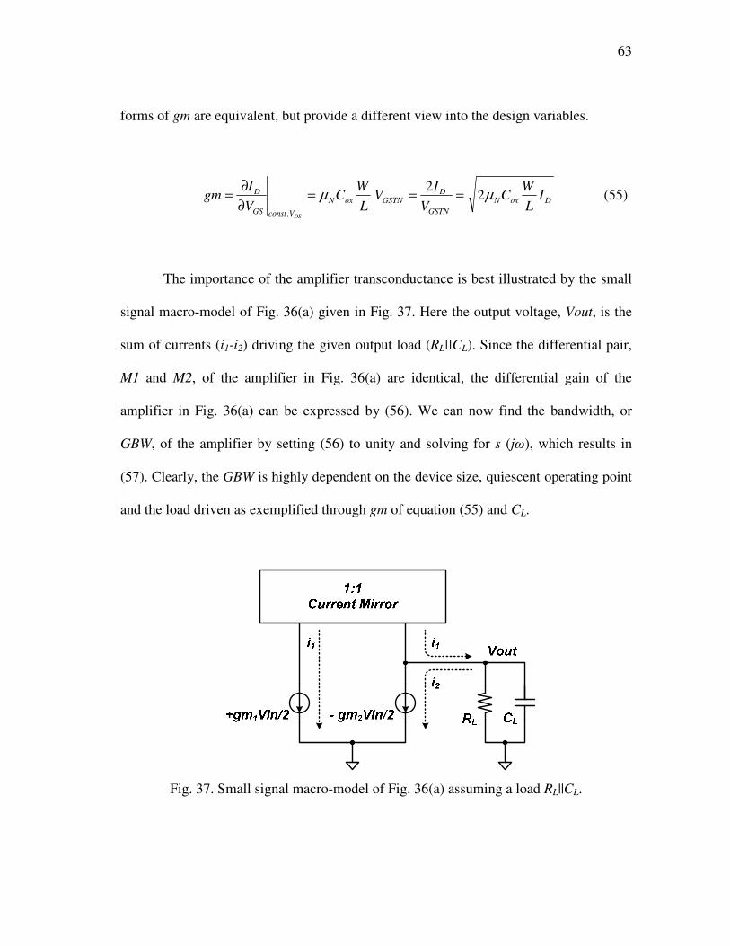
63
forms of gm are equivalent, but provide a different view into the design variables.
DoxN
GSTN
DGSTNoxN
VconstGS
D IL
WC
V
IV
L
WC
V
Igm
DS
µµ 22
.
===∂
∂= (55)
The importance of the amplifier transconductance is best illustrated by the small
signal macro-model of Fig. 36(a) given in Fig. 37. Here the output voltage, Vout, is the
sum of currents (i1-i2) driving the given output load (RL||CL). Since the differential pair,
M1 and M2, of the amplifier in Fig. 36(a) are identical, the differential gain of the
amplifier in Fig. 36(a) can be expressed by (56). We can now find the bandwidth, or
GBW, of the amplifier by setting (56) to unity and solving for s (jω), which results in
(57). Clearly, the GBW is highly dependent on the device size, quiescent operating point
and the load driven as exemplified through gm of equation (55) and CL.
Fig. 37. Small signal macro-model of Fig. 36(a) assuming a load RL||CL.
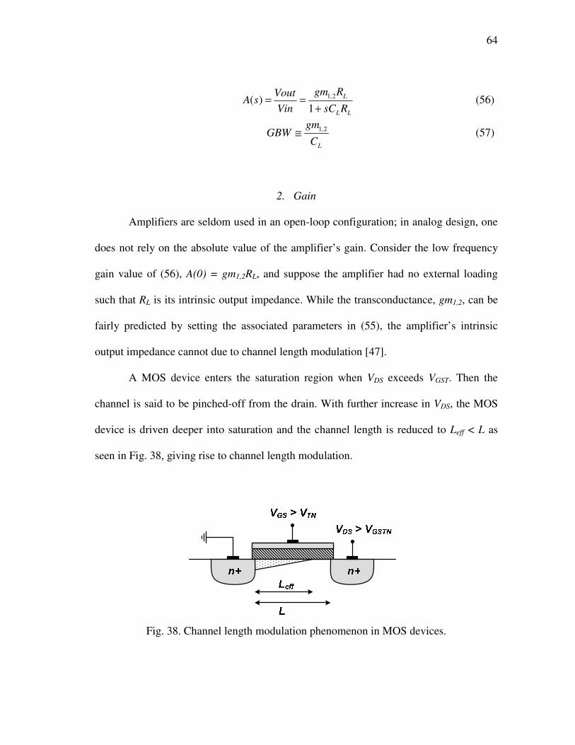
64
LL
L
RsC
Rgm
Vin
VoutsA
+==
1)( 2,1 (56)
LC
gmGBW
2,1≅ (57)
2. Gain
Amplifiers are seldom used in an open-loop configuration; in analog design, one
does not rely on the absolute value of the amplifier’s gain. Consider the low frequency
gain value of (56), A(0) = gm1,2RL, and suppose the amplifier had no external loading
such that RL is its intrinsic output impedance. While the transconductance, gm1,2, can be
fairly predicted by setting the associated parameters in (55), the amplifier’s intrinsic
output impedance cannot due to channel length modulation [47].
A MOS device enters the saturation region when VDS exceeds VGST. Then the
channel is said to be pinched-off from the drain. With further increase in VDS, the MOS
device is driven deeper into saturation and the channel length is reduced to Leff < L as
seen in Fig. 38, giving rise to channel length modulation.
Fig. 38. Channel length modulation phenomenon in MOS devices.

65
The channel length modulation can be incorporated in the square law I-V model
of (53) to yield (58), where ID0 is the ideal drain current expressed by (53). Using (58)
we can express the intrinsic output impedance of a MOS device as in (59). We can again
derive the transconductance, gm, from (58) and together with (59), express the intrinsic
gain Ai = gm rds of a MOS device as in (60).
( ) ( )DSDDSGSToxGST
eff
oxD VIVVL
WCV
L
WCI λλµµ +=+≡= 11
2
1
2
10
22 (58)
0
2
.
1
12
DGSTNoxNVconst
DS
Dds
IVWC
L
V
Ir
GS
λλµ==
∂
∂=
−
(59)
( )
GSTN
DSi
V
VA
λ
λ+=
12 (60)
Equations (59) and (60) demonstrate the uncertainty in the intrinsic output
impedance and gain of a MOS device, and hence of an amplifier. However, because
amplifiers are used in a closed loop configuration, i.e. using feedback, this gain
uncertainty is of little concern. Fig. 39 shows a simple example of an amplifier in closed
loop for which the gain Vout/Vin is given by (61). For a sufficiently large intrinsic
amplifier gain A, Vout/Vin is virtually independent of A and is set by the capacitor ratio
C1/C2. Nonetheless, (60) highlights the importance of the quiescent operating point of
the MOS device, and can give an approximate measure of the maximum intrinsic MOS
gain achievable for a particular CMOS technology.

66
Fig. 39. An example of a closed loop amplifier circuit.
++−−≅
+++−=
−
2
21
2
1
1
2
21
2
1 11CA
CCC
C
C
CA
CCC
C
C
Vin
Vout PP (61)
What is critical for low voltage applications and can be deduced from (60) is how
the amplifier gain is related to the output swing. For large signals, the quiescent
operating point of a MOS device can no longer be considered fixed as with small
signals, but is incrementally changing; as the output swings closer to either supply rail,
the quiescent VDS of the respective device decreases and hence the gain is reduced. This
has to be closely considered in low voltage applications, where the signal swing needs to
be maximized while maintaining the highest gain possible.
3. Phase Margin
Although the macro-model of Fig. 36(a) provides a good approximation of the
small signal amplifier behavior, it overlooks the parasitics of the current mirror now
modeled in Fig. 40. The mirrored current, i*
1, is no longer identical to the source i1,

67
which modifies the overall gain expression as given by (62). Unlike (56), the gain
expression in (62) is a two-pole system, and its significance is best explained by
examining the phase of Vout. Since the amplifier transfer function is variable with
frequency, it results in a magnitude and phase change at the output. Given the complex
nature of the gain expression (s=jω), the phase is given by the cumulative effect of the
poles and zeros, and the general phase expression is given by (63) for a transfer function
with n poles (ωp) and m zeros (ωz).
Fig. 40. Improved small signal macro-model of Fig. 36(a).
( ) ( )( )( )43
432,1
2
*
111
2/1
1)(
,GSLL
,GSL
LL
L
gmCsRsC
gmsCRgm
RsC
Rii
Vin
VoutsA
++
+=
+−≅= (62)
∑∑=
−
=
−
−
=
m
k zk
n
l pl 1
1
1
1 tantan)(ω
ω
ω
ωωθ (63)

68
Using (63) we can express the phase of (56) and (62) as in (64) and (65)
respectively, where CGS = Cgs3+Cgs4. From (64) and (65), we see the phase is negative
and decreasing with frequency in the presence of poles. This is potentially problematic
with closed-loop amplifier configurations such as in Fig. 39, and detailed analyses are
presented in [50]-[51]. However, an intuitive way to analyze this is as follows. The
magnitude of the amplifier transfer function is generally a decreasing function of s,
similar to (56) and (62). Suppose for some transfer function with multiple poles that the
phase shift between Vout and Vin exceeds 180° at some frequency ωo while the
amplifier’s gain is greater than unity (ωo < GBW), then the output of the amplifier in Fig.
39 will oscillate indefinitely and become unstable.
−= −
LLiii RC1
tan)( 1
)5(
ωωθ (64)
+
−
−= −−−
GSGSLLiii CgmCgmRC 4,3
1
4,3
11
)11( 2tantan
1tan)(
ωωωωθ (65)
The phase margin is a measure of how far is the amplifier from being unstable
and is measured at s=GBW. The phase margin is also a good indicator to the amplifier
ability to reach steady state should a fast time-varying signal, such as a step function, be
applied to its input. This is illustrated in Fig. 41 by considering the 0.1% step response
settling time of the amplifier in Fig. 36(a) when used as in Fig. 39 for C1 = C2, CP = 0,
A(0) = 60dB, GBW =100MHz and different phase margin values.

69
Fig. 41. Closed loop step response of the amplifier in Fig. 36(a) for different phase
margin values.
The results of Fig. 41 lead to the conclusion that a phase margin around 60° is
ideal for high speed performance. Indeed, this is the case for the chosen settling error
(0.1%) and if there are no pole-zero doublets within the amplifier’s GBW. If on the other
hand the latter is the case, the frequency of the doublet and separation between the pole
and zero can dominate the settling behavior and significantly slow down the amplifier’s
response [52]-[53].
The amplifier architecture can also play a role in determining the speed. The
transfer function of (62) demonstrated that the presence of the current mirror M3:M4 in
Fig. 36(a) led to the addition of a pole-zero pair that may hinder the speed of the
amplifier if not considered in design. On the other hand, the fully differential amplifier
in Fig. 36(b) does not suffer the same limitation. Fig. 42 shows the macro-model of the

70
fully differential amplifier in Fig. 36(b) and (66) describes the amplifier’s transfer
function. Note that (66) is identical to (56). Unlike the single ended amplifier, the two
signal paths in the fully differential amplifier are identical and their summation at the
output does not generate a pole-zero pair that can slow down the speed. This is one of
numerous advantages for using fully differential amplifiers over their single ended
counterparts.
+gm1Vin/2
- gm2Vin/2RL CL
Vout +
i2
RLCL
Vout -
i1
Fig. 42. Small signal macro-model of Fig. 36(b) assuming a load RL||CL.
( ) ( )
LL
L
RsC
Rgm
Vin
VoutVoutsA
+=
−−+=
1)(
2,1. (66)
4. Slew Rate
In SC application, the settling time and accuracy of a circuit is crucial to good
linearity. Consider the single ended amplifier of Fig. 36(a) configured as in Fig. 39, and
for simplicity refer to its gain transfer function as in (56). The time-domain step response
can then be described by (67), where the feedback factor, β, is C2/(C1+C2+CP), and
closed loop amplifier gain, α, is given by (68).

71
( )tGBWeVinVout ⋅⋅−−⋅−= βα 1 (67)
1
2
1
)0(
11
−
+=
AC
C
βα (68)
Given sufficient time, the final value is that described by (61). However, the
maximum time allocated for the amplifier to settle is limited by half the sampling clock
period, TS. This emphasizes the maximization of the amplifier GBW through circuit
configuration selection, and β through input parasitic consideration, especially when
high accuracy settling is desired. However, this is only half the picture.
Equation (67) holds true if and only if the amplifier is capable of handling any
level of input. In reality the amplifier’s ability to drive current into its output impedance
is generally limited by the amount of current available to bias it. In Fig. 36, M0 is
referred to as the tail of the amplifier, which provides the tail current IT. For large step
inputs, one of the input drivers enters into the subthreshold region (shuts off), while the
other is strongly driven to conduct all of IT. The current IT is then driven directly, or
indirectly through the current mirror, into the output load. In this operation mode, the
amplifier is said to be slewing, and the linear settling behavior described by (67) is no
longer valid. The rate at which the output voltage changes with respect to time in the
slewing mode defines the slew rate, SR, of the amplifier as described by (69).
L
T
C
I
t
VoutSR =
∂
∂= (69)

72
Now it can be shown that Vout may be expressed by (70) when the slew rate is
taken into account for zero initial conditions [54]—derivations are also available in
appendix A. Furthermore, given an absolute settling error εS, the overall settling time tS
is expressed by (71) and the slewing time tslew and linear settling time tlin are given by
(72) and (73) respectively.
( )
( )
≤−⋅−
>
⋅
⋅⋅⋅−⋅−
<⋅
=
⋅⋅−
−⋅−
0,1
,1
,
slew
tGBW
slew
ttGBW
slew
teVin
tteGBWVin
SRVin
tttSR
Vout slew
β
β
α
βαα (70)
−
⋅⋅⋅⋅+
⋅=+= 1ln
1
GBWVin
SR
GBWSR
Vinttt
S
linslewSβαεβ
α (71)
GBWSR
Vintslew
⋅−
⋅=
β
α 1 (72)
⋅⋅⋅⋅=
GBWVin
SR
GBWt
S
linβαεβ
ln1
(73)
The fastest settling performance is inarguably that for all-linear settling, which
can be proven by taking the derivative of (71) with respect to SR, and substituting the
outcome in (72). More importantly, however, using (72) we can find the maximum input
step for which no slewing will occur. The result is given by (74).
βαβα ⋅
=⋅⋅
≤ GST
slewno
V
GBW
SRVin (74)
73
The expression in (74) shows that slewing is inevitable for high speed Nyquist
rate SC applications such as pipeline ADCs. In such applications the input step size
between consecutive cycles can be in the order of the system’s full-scale voltage, VFS,
which is much larger than (74) predicts. In part, the amplifier’s input pair VGST is limited
to the range of 100-200mV to maximize signal headroom and input common mode
range. On the other hand, α and β are set by the amplifier’s configuration and their
product can loosely be considered unity for high speed designs. These conditions yield a
maximum non-slewing step of roughly 0.2 VFS in present-day CMOS technologies.
Therefore the only viable approach to reducing the settling time is to enhance both SR
and GBW of the amplifier, and hence it is critical to account for the amplifier slewing
performance in the power budget.
5. Distortion
By examining the square law I-V relationship in (53) we can conclude that the
MOS transistor is not a linear device. However, through the use of feedback, CMOS
amplifiers are used successfully to implement highly linear functions. Intuitively,
because of the high amplifier gain, the positive and negative input terminals of the
amplifiers experience a virtual short; that is the amplifier’s input terminals seem fixed
about the ideal quiescent operating point for any input signal.
The paradox of feedback, however, is the use of a non-linear device to linearize
itself. The transfer function described by (61) is ideally given by the ratio C1/C2, but the
finite amplifier gain results in an error term. When an input is applied, the output swing

74
modulates the VDS of the output devices thereby changing the amplifier gain and
subsequently the error term in the transfer function. To reflect this behavior, (61) is
modified to (75) where the gain is now a function of the input. Also, Fig. 43 depicts this
graphically for the absolute values of (61) and (75). The result is an input dependent gain
error for large output swings and consequently observable distortion at the output, which
is undesirable in many applications such as pipeline ADCs.
++−−≅
+++−=
−
2
21
2
1
1
2
21
2
1
)(1
)(1
CVinA
CCC
C
C
CVinA
CCC
C
C
Vin
Vout PP (75)
Fig. 43. Amplifier gain degradation for large output swings.
Another source of distortion is the SR limited settling. Consider the flip-around
S/H amplifier discussed in Chapter III. For the case of all-linear settling, the final output
is expressed by (76) where all parameters with the SH subscript have the same previous

75
definitions, but pertaining to the flip-around S/H. Note that the error term is independent
of Vin and therefore is a fixed for all input values. If the settling becomes SR limited,
however, then the output is expressed by (77).
−−=
−21S
SH
TGBW
SH eVinVoutβ
α (76)
>
⋅
⋅−−
≤
−−
=
−+−
−
SHSH
GSTSR
VinTGBW
SHSH
SHSH
SHSH
GSTT
GBW
SH
SHSH
SHSSH
SH
SSH
VVine
GBWVin
SRVin
VVineVin
Vout
βαβαα
βαα
αβ
β
,1
,1
21
2
(77)
From (76) we conclude that for the all-linear settling, the value of TS/2 is
irrelevant as far as distortion is concerned, because it will result in a consistent gain error
for all values of Vin. The same is true for the SR limited settling, but for a small range of
input values. As Vin crosses the limit described in (74), the settling error becomes input
dependent and results in distortion. This is depicted in Fig. 44, where the thick solid
trace is the input, and thin solid trace and dotted trace are the all-linear and SR limited
settling of the S/H output respectively. The upper traces are the real-time waveforms,
while the bottom traces are the end-points plot of the S/H output in the hold phase. Note
that the input trace is shifted forward in time by half a clock cycle to correspond to the
end points of the S/H traces. In the shaded regions of Fig. 44, the output is compressed
for the SR limited case, whereas otherwise it follows the all-linear settling curve.

76
Therefore, when considering SC linear applications, the linearity is often
expressed as a maximum settling error specification; say εmax, which for the S/H example
above is expressed by (78).
Fig. 44. Slew rate induced distortion for fixed settling time, TS/2; thick solid: Vin, thin
solid: Vout (linear settling) and dashed: Vout (slew rate limited settling).
SHSH
GSTSR
VinTGBW
SHSHSH
SH SHSH
SHSSHSH V
VineGBWVin
SR
βαβαε
αβ
>⋅⋅
≥
−+−
max
21
max
max ,
max
(78)
6. Noise
Noise in circuits can be generally defined as spontaneous fluctuations in current,
voltage or temperature that set the lower limit on measurements taken on a system under
test [55]. In many applications, such as data converters, continuous time filters and audio

77
amplifiers, these fluctuations are the limiting factors in a design’s dynamic performance.
There are two dominant noise sources that affect the performance of CMOS
circuits, namely the thermal and flicker noise. Thermal noise is attributed to the random
charge carrier motion in a conductor due to the ambient temperature. As for the flicker
noise, the major contributor is the interaction of the charge carriers with the Si-SiO2
interface, where the carriers are trapped and then released back into the channel in a
random process [55]. These noise sources can be modeled in MOS devices as a current
source in parallel with the device representing the power spectral density, which is given
by (79) where the first and second terms represent the thermal and flicker noise
contributions respectively. Here, kB, T, γ, KF and f represent Boltzman’s constant, the
absolute temperature, noise factor, process dependent flicker noise coefficient and
frequency respectively. Equation (79) is a simplified form of other complex models [56]-
[57], but is very useful for design.
ffLC
IKgmTki
ox
DFo ∆γ ⋅
+=
2B
2 4 (79)
To aid the derivation of the amplifier noise, we refer to the amplifier noise model
in Fig. 45 from which we can express the maximum noise seen at the output by (80). To
minimize clutter, the thermal and flicker noise components will be examined separately
by substituting (79) into (80).
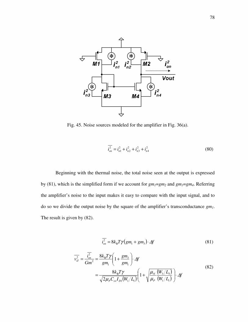
78
2
1ni2
2ni
2
3ni2
4ni
2oni
Fig. 45. Noise sources modeled for the amplifier in Fig. 36(a).
2
4
2
3
2
2
2
1
2
nnnnon iiiii +++= (80)
Beginning with the thermal noise, the total noise seen at the output is expressed
by (81), which is the simplified form if we account for gm1=gm2 and gm3=gm4. Referring
the amplifier’s noise to the input makes it easy to compare with the input signal, and to
do so we divide the output noise by the square of the amplifier’s transconductance gm1.
The result is given by (82).
( ) fgmgmTkion ∆γ ⋅+= 31B
2 8 (81)
( )( )( )
fLW
LW
LWIC
Tk
fgm
gm
gm
Tk
Gm
iv
P
N
DoxP
oniT
∆µ
µ
µ
γ
∆γ
⋅
+=
⋅
+==
11
33
111
B
1
3
1
B
2
22
12
8
18
(82)

79
Following the same approach with respect to the flicker noise component, the
output noise and input referred noise are given by (83) and (84) respectively. Note that
the results of (81)-(84) are the same for the fully differential amplifier of Fig. 36(b) since
the sum of currents at the output is the same.
fL
K
L
K
fC
Ii FNFP
ox
Don ∆⋅
+=
2
3
2
1
2 22 (83)
fL
L
K
K
fCLW
K
fL
K
L
K
fCgm
I
Gm
iv
FP
FN
oxP
FP
FNFP
ox
Don
fi
∆µ
∆
⋅
+=
⋅
+==
2
3
1
2
11
2
3
2
1
2
1
2
22
1
1
2
(84)
There are a few conclusions that can be drawn from (82) and (84) regarding the
amplifier’s noise. First, and foremost, the gm of the input pair has a huge impact on the
overall amplifier noise performance. Note that referring the output noise to the input was
done through the input pair gm, and hence it is crucial to maximize the input gm beyond
any other transistor; in a truly low noise amplifier, the maximum gm is that of the input
pair. Second, the sizing plays a direct role in the noise performance. From (82) we see
the ratio of the dimensions of M1 and M3 and also in (84) in terms of the channel length
and input pair area. Moreover, a closer look at (84) shows that the flicker noise
expression is a quadratic function of L1, and hence there exists a value for L1 at which
the flicker noise is minimized and is given by (85).

80
FN
FP
K
KLL 31 = (85)
Finally, the device type is also a factor in the amplifier’s noise. Both (82) and
(84) contain parameters that are device type dependent, namely the mobility µN,P and the
flicker noise coefficient KFN,P. This brings up the question of which device type is most
suitable for the input pair for the best noise performance. To answer part of the question,
let us first consider the device mobility. The electron mobility µN is 3-4 times faster than
the hole mobility µP in semiconductors [58]-[59], and hence it is best to use NMOS
devices as the input pair to minimize the thermal noise.
On the other hand, in CMOS technologies the transistors gates are commonly n+
polysilicon, which result in a buried-channel-like behavior for PMOS devices that
minimizes the interaction of the carriers with the Si-SiO2 interface and consequently the
flicker noise coefficient [60]-[62]. This results in KFP to be an order of magnitude
smaller than KFN, and hence PMOS devices are ideal as input pair devices to minimize
the flicker noise. For p+ polysilicon gates, however, KFP and KFN are of the same order.
Therefore, the answer as to which device type is more suitable for low noise
amplifier design seems different for each type of noise. Nonetheless, in light of the
advancement of CMOS technologies, the contribution of each noise type is also
different. From (79), the thermal noise has a flat behavior with frequency, while the
flicker noise is inversely proportional to frequency. Equating the two noise components
and solving for f, yields the noise corner frequency, fnc, given by (86).

81
22 84 LCTk
VK
LgmCTk
IKf
oxB
GSTF
oxB
DFnc
γγ== (86)
Using (86), the noise corner frequency of present-day CMOS technologies is in
the 100s of MHz, which makes the flicker noise the major contributor to amplifier noise
in many applications. Hence, for overall noise performance, it is generally better to use
PMOS devices as the input pair of amplifiers.
In summary, to optimize the noise performance of amplifiers for high speed, low
voltage and low power applications, one can follow these guidelines:
Use PMOS devices for the input pair, unless p+ polysilicon is used for the gate
material, or extremely high speed applications (GHz range) are targeted.
Maximize ID of the input pair within the given power budget.
Maximize the area and the aspect ratio of the input pair devices (WL and W/L).
Once all device aspect ratios are defined, use (85) to set the value of the input
pair channel length, but maintain the aspect ratio.
7. Process Variations
Amplifiers are ideally symmetric by design, but once fabricated a zero-input
signal commonly results in a finite output. This behavior is attributed to minor
asymmetries that are either systematic or random but together constitute what is known
by offset. Systematic offset is imposed on the amplifier by the design and choice of

82
quiescent operating points of devices and can be reduced by good design practices.
Random offset, on the other hand, is the result of manufacturing process variations.
Manufacturing process variations are a result of finite lithography resolution,
non-uniform oxide thickness growth and doping profiles across the wafer’s plane. A
mismatch model [63] based on the study of equal area rectangular devices, states that the
one-dimensional variance of a parameter P can be expressed by (87) where AP is the area
proportionality constant for parameter P, W and L are the device dimensions, SP is the
variation of P with spacing, and Dx is the distance between two devices along x. In
practice, critical devices such as the input pair or current mirrors are interdigitated or
cross-coupled, and hence Dx approaches zero, and the second term of (87) can be
neglected. Using (53), the drain-current variance due to process variation can be
expressed as in (88) assuming σ2(VT) and σ
2(βI) are uncorrelated [63]-[66]. Here βI
represents µCoxW/L. Equation (88) is very useful, because from a circuit analysis stand
point, the drain-current variance can be treated as a small signal that can be referred to
the gate of the MOS device through its transconductance, gm. The result is given by
(89).
( ) xPP DS
WL
AP
22
2 +=σ , (87)
( ) ( ) ( )2
22
2
222 4
I
ID
GST
TDD I
V
VII
β
βσσσ += (88)
( ) ( )( )
( )2
2
2
22 1
I
I
D
TGSIgm
VVβ
βσσσ += (89)

83
It was demonstrated in [67] that for nominal biasing conditions (VGST < 650mV),
σ2(VT) is the dominant mismatch factor. Moreover, in analog design the term gm/ID is
generally maximized, which further supports the dominance of σ2(VT) and reduces the
effect of the second term of (89). Therefore, we can reduce (89) to (90) to describe the
gate-referred (input-referred) current variance in MOS devices. HereTVA is the area
proportionality constant for the threshold voltage, VT.
( ) ( )WL
AVV TV
TGS
2
22 =≅ σσ (90)
Using (90), the input offset variance can be expressed as the sum of all device
drain current variances at the amplifier’s output, and then referred to the input using the
amplifier’s gm. This analysis is quite similar to the noise analysis and the noise model of
Fig. 45 can be used here, but with the substitution of σ2(ID) = gm
2σ
2(VGS) for 2
ni . Thus,
the total output current variance and input offset variance of the amplifier in Fig. 36(a)
are given by (91) and (92) respectively, which again is the simplified form if we account
for gm1=gm2 and gm3=gm4.
( )
+
=
33
2
2
3
11
2
2
1
2 2LW
Agm
LW
AgmI TNTP VV
outputDσ (91)
( )
+=
+
=
2
3
1
2
11
2
33
2
2
1
2
3
11
2
2 122L
L
A
A
LW
A
LW
A
gm
gm
LW
AV
TP
TNTPTNTP
V
V
P
NVVV
OSµ
µσ (92)
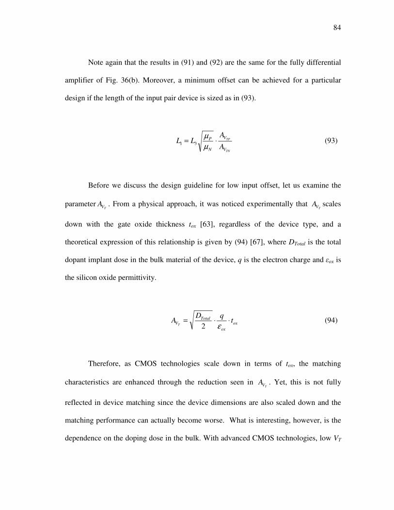
84
Note again that the results in (91) and (92) are the same for the fully differential
amplifier of Fig. 36(b). Moreover, a minimum offset can be achieved for a particular
design if the length of the input pair device is sized as in (93).
TN
TP
V
V
N
P
A
ALL ⋅=
µ
µ31 (93)
Before we discuss the design guideline for low input offset, let us examine the
parameterTVA . From a physical approach, it was noticed experimentally that
TVA scales
down with the gate oxide thickness tox [63], regardless of the device type, and a
theoretical expression of this relationship is given by (94) [67], where DTotal is the total
dopant implant dose in the bulk material of the device, q is the electron charge and εox is
the silicon oxide permittivity.
ox
ox
TotalV t
qDA
T⋅⋅=
ε2 (94)
Therefore, as CMOS technologies scale down in terms of tox, the matching
characteristics are enhanced through the reduction seen in TVA . Yet, this is not fully
reflected in device matching since the device dimensions are also scaled down and the
matching performance can actually become worse. What is interesting, however, is the
dependence on the doping dose in the bulk. With advanced CMOS technologies, low VT

85
devices are becoming more robust and their use in low voltage applications more
diverse. Their lower VT is achieved by a counter type implant in the bulk region
immediately under the gate where the channel is formed. This effectively reduces the
total dose and improves their matching performance over regular devices.
In conclusion, the following design guidelines can be adopted for low input
offset amplifiers:
Maximize the width of the input pair devices.
Maximize the length of devices apart from the input pair.
Set the input pair device length as given by (89).
Use low VT devices if they can support the design requirements.
The best type of device for the input pair is dependent on theTVA parameter for
each device type.
B. Amplifiers for Pipeline ADCs
The preceding discussion demonstrated the many aspects of amplifier design, and
the choice of the amplifier architecture to use in a pipeline cell must consider all to
guarantee proper performance within the boundaries imposed by power and area. Fig. 46
shows the three fundamental topologies that are commonly seen in pipeline ADCs, and
they are the Telescopic, Current Mirror and Folded Cascode OTAs. The following is a
brief comparison of each and a presentation of their key performance metrics; detailed
expressions of their performance metrics are given in Appendix C.

86
K I
T/2
K I
T/2
I T/2
I T/2
K I
T/2
K I
T/2
Fig. 46. Fundamental OTA architectures; (a) telescopic, (b) current mirror
and (c) folded cascode.
If we assume the transconductance gm1 of M1 to be the same for all amplifiers in
Fig. 46, then the summary of parameters in Table 3 can easily be used to summarize the
strengths and weakness of each amplifier topology as follows.

87
TABLE 3
FUNDAMENTAL PARAMETER SUMMARY OF OTAS SEEN IN FIG. 46
Parameter Telescopic Current Mirror Folded Cascode
Minimum Supply satDSGS VV ,3+ satDSGS VV ,2+ satDSGS VV ,2+
Maximum Signal Swing satDSDD VV ,5− satDSDD VV ,4− satDSDD VV ,4−
Total Current (ITOT) TI ( )KIT +1 TI2
Transconductance (Gm) 1gm 1Kgm 1gm
LHP Poles 2 3 2
Slew rate (for a CL load) L
T
C
I
L
T
C
KI
L
T
C
I
Input Referred Thermal
Noise ( )1316 gmkT∗
+
1
71gm
gm
+++
1
2
115
1
31gmK
gmgm
gm
gm
++
1
931gm
gmgm
Efficiency (Gm/ITOT) TI
gm1 TIK
Kgm
)1(
1
+
TI
gm
2
1
The Telescopic OTA is undoubtedly the most power efficient amplifier. It also
has the best frequency response in term of the number of poles and zeros and their
locations, and the least noise contribution. On the other hand, it requires a higher supply
than both the Current Mirror and Folded Cascode OTAs, and leaves the least headroom
for signal swing at the output, which makes it the least suitable for low voltage
applications despite its other strengths. Overall, the Telescopic OTA is best suited for
designs that require very high speed and low noise performance where the signal swing
is not very critical.
The Current Mirror OTA is superior to the Telescopic in term of low voltage

88
operation. It can also deliver a higher slew rate performance and a wider GBW, but at
the expense of higher power dissipation. However, its noise contribution is the highest of
all amplifiers, and its efficiency is lesser than that of the Telescopic OTA. Furthermore,
while the efficiency can be enhanced by increasing K, the frequency response is
degraded as K plays a significant role is the placement of one of its poles. Overall, the
Current Mirror OTA is best suited for low voltage and large signal swing applications,
where the noise, speed and power performances are not very critical.
Finally, the Folded Cascode OTA is the comfortable medium of both the
Telescopic and Current Mirror OTA. It shares a good low voltage performance with the
Current Mirror OTA, but without the additional noise. It also shares a very good
frequency performance with the Telescopic OTA, but a degraded efficiency. Overall, the
Folded Cascode OTA is suitable for a larger range of applications where speed, noise
and signal headroom are valued. It is not surprising then to see the increased use of the
Folded Cascode amplifier in the literature in state-of-the-art designs whether as a single
stage or the first stage in a multi-stage amplifier [26], [68]-[73].
C. Amplifier Enhancement
Some of the amplifier requirements needed to implement pipeline cells cannot be
satisfied by a simple OTA as those presented in section B. For example, a 200MS/s 10bit
resolution MDAC requires an amplifier with a minimum gain of 66dB to keep the static
settling errors within ½ LSB. Yet, in modern CMOS technologies the gain attainable by
any of the OTAs in Fig. 46 may not exceed 50dB while operating at that speed. To

89
overcome this limitation, amplifier enhancement techniques are widely used with the
most common being multi-stage cascading and regulated cascode gain boosting.
1. Multi-Stage Amplifiers
Gain enhancement using multi-stage amplifiers is a well-established technique
that relies on the cascading of two or more gain stages as depicted by the Miller
compensated example in Fig. 47. The low frequency gain of the multi-stage amplifier is
the product of all cascaded gain stages; A = A1A2 for the example in Fig. 47. However,
each additional gain stage introduces another low frequency pole, which limits the
bandwidth of the amplifier and more importantly increases the risk of instability.
Therefore, multi-stage amplifiers utilize different compensation techniques to overcome
such limitations [74], and the most popular is the Miller compensation represented by
the dashed lines in Fig. 47.
Fig. 47. Miller compensated multi-stage amplifier.
In addition to the increased gain of the overall amplifier, multi-stage amplifiers
can utilize the full supply range for signal swing by adopting a rail-to-rail output stage.

90
This is a significant advantage in low voltage applications as it maximizes the noise
tolerance. However, multi-stage amplifiers are often bulky and power hungry due to the
use of compensation capacitors, and while some techniques attempt to alleviate these
drawbacks, multi-stage amplifiers are still no match to the speed and power efficiency of
a single stage amplifier.
2. Gain Boosting
Another amplifier enhancement technique is the regulated cascode gain boosting.
Instead of cascading several amplifiers to increase the gain, the regulated cascode gain
boosting approach relies on active feedback to limit the VDS variations at the source of
the cascode device. This is illustrated in Fig. 48 for a Telescopic OTA, but can readily be
applied to Current Mirror and Folded Cascode OTAs as well.
The feedback loop of the auxiliary amplifier and the cascode transistor enhances
the output impedance, and thus increases the amplifier gain [75]. An advantage of this
approach over multi-stage amplifiers is the transparency of the gain enhancement to the
signal path; it does not add low frequency poles that slow down the amplifier or
compromise its stability. However, as is the case with any feedback loop, some
conditions must be satisfied as expressed by (95). Namely, the GBW of the auxiliary
amplifier needs to be greater than the closed loop bandwidth of the main amplifier, and
less than its non-dominant pole; the first condition guarantees no pole-zero doublets
within the closed loop bandwidth that may introduce slow settling components, while the
second ensures the stability of the auxiliary amplifier and cascode transistor loop.

91
opampmainPBoostinguLoopCloseddB 23 ωωω <<− (95)
VCMFB
Vin-Vin+
Vout-
GND
Vbp1
VDD
M1 M2
M3 M4
M5 M6
M7 M8
M0
IT
IT/2IT/2
Vout+
-A -A
-A -A
Fig. 48. Regulated cascode gain boosting applied to a telescopic OTA.
Overall, as the auxiliary amplifiers only drive their respective cascode device,
they are quite small, which makes the regulated cascode gain boosting method more
efficient than utilizing a multi-stage amplifier from a power and area stand point.
However, the main drawback to the regulated cascode approach is the limited head for
the output swing.

92
D. Conclusions
Numerous aspects of amplifier design have a direct impact on the performance of
pipeline cells. Through a systematic approach, key performance metrics of amplifiers
were derived and discussed with a focus on building robust amplifiers for the application
of high speed, high resolution and high efficiency S/H and MDAC pipeline cells.
Particular emphasis was given to distortion, noise and offset as they are detrimental to
the operation of such cells. Moreover, a survey of the fundamental OTA architectures is
undertaken to isolate the best overall design for high speed, low voltage and low power
applications. Finally, the widely used gain enhancement techniques are described, and
for optimum efficiency the regulated cascode gain boosting approach is recommended.
However, a combination of gain boosted first stage followed by a rail-to-rail output stage
serves as the best compromise.

93
CHAPTER V
RECYCLING FOLDED CASCODE*
Chapter IV highlighted the strengths of the Folded Cascode (FC) amplifier,
which recently has become one of the most commonly used amplifier architectures in
low voltage pipeline ADCs whether in the single or multi-stage form. Therefore, it is not
surprising to see efforts in the literature aimed to enhance its performance, and other
amplifiers in general.
Earlier work to enhance the performance of the FC used multi-path schemes [76]
and [77]. Other multi-path schemes such as [78] and [79] were applied to the Current-
Mirror OTA to specifically enhance the output impedance and slew rate, and to emulate
a class AB output stage operation. The concept behind these schemes is to split the input
signal among several paths whose sum at the amplifier output is in phase—similar to a
current mirror active load in single-ended amplifiers. This may result, however, in
numerous low frequency pole-zero pairs in the amplifier’s open loop transfer function
that may render it useless for high speed applications such as in Nyquist ADCs. While
[76]-[79] may fall in that category of slower amplifiers, they nevertheless form the basis
of the proposed modification to the FC amplifier presented in Section A.
* Part of the data reported in this chapter is reprinted with permission from “The recycling folded cascode:
a general enhancement of the folded cascode amplifier,” by R. S. Assaad and J. Silva-Martinez, 2009.
Journal of Solid-State Circuits, vol. 44, no. 9, pp. 2535-2542, Copyright 2009 by IEEE. This material is
posted here with permission of the IEEE. Such permission of the IEEE does not in any way imply IEEE
endorsement of any of Texas A&M University’s products or services. Internal or personal use of this
material is permitted. However, permission to reprint/republish this material for advertising or promotional
purposes or for creating new collective works for resale or redistribution must be obtained from the IEEE
by writing to [email protected]. By choosing to view this material, you agree to all provisions of
the copyright laws protecting it.

94
A. Proposed Folded Cascode Amplifier
The conventional FC is shown again in Fig. 49 for convenience. Note how
transistors M3 and M4 are the two transistors in the signal path that conduct the most
current, and in many designs have the largest transconductance. However, their role is
strictly limited to providing a folding node for the small signal current generated by the
input differential pair M1 and M2.
Fig. 49. The conventional folded cascode amplifier.
To address this inefficiency, a modified FC amplifier is presented in Fig. 50. The
proposed modifications are intended to use M3 and M4 as driving transistors [80], and
proceed as follows. First, the input differential pair, M1 and M2 (Fig. 49), are split in
half to produce transistors M1a, M1b, M2a, and M2b (Fig. 50). Next, M3 and M4 (Fig.

95
49) are split to form the current mirrors M3a:M3b and M4a:M4b with a ratio of K:1
(Fig. 50), where K is chosen to be 3 strictly to maintain the same current consumption as
the FC in Fig. 49; naturally K has to be greater than 1 to maintain current in the output
devices M5-M10. The diode connected transistors, M3b and M4b, are cross-coupled with
the input transistors, M2b and M1b, to ensure the small signal currents added at the
sources of M5 and M6 are in phase. Finally, cascode devices may be added inside the
diode connection of M3b and M4b to reduce the current dependency on VDS and improve
matching in the current mirrors. The modified Folded Cascode will be referred to by the
Recycling Folded Cascode (RFC), since we are reusing, or recycling, existing devices
and currents to perform an additional task.
Fig. 50. The recycling folded cascode (RFC) amplifier.

96
B. Recycling Folded Cascode Characteristics
The modifications presented in Section A provide the RFC with enhanced
features over the FC. In this section, various amplifier merits will be derived for the RFC
to present these enhancements quantitatively, similar to Chapter IV. This will also help
examine the costs associated with the proposed modifications from a design perspective.
1. Small Signal Transconductance
We first examine the amplifier’s transconductance, Gm. By finding the short-
circuit current at the output of the RFC with respect to its input, its small signal
transconductance can be expressed as in (96). Since M1 in the original FC is twice the
size of M1a and conducts twice the amount of current for the same bias conditions, then
gm1,FC = 2gm1a,RFC. Using this result and by substituting for the value of K = 3 in (96),
the low frequency transconductance of the RFC is demonstrated to be twice that of the
FC for the same power consumption. In other words, for the same capacitive load, the
GBW of the RFC is twice as wide as that of the FC.
( )KgmGm aRFC += 11 (96)
2. Low Frequency Gain
It was demonstrated that GmRFC = 2GmFC, which results in a 6dB gain
enhancement for the same output impedance. However, RoRFC is also enhanced over
RoFC. The expression for RoRFC is given by (97) and that of RoFC by (98). Because of the

97
modifications in RFC, M2a and M4a conduct less current than their counterparts M2 and
M4 of the FC, which enhances their intrinsic output impedance, rds. It is this
enhancement in rds2a and rds4a that adds an additional 2–4dB to the gain of the RFC.
Therefore, an overall low frequency gain enhancement of 8−10dB can be seen in the
RFC compared to the FC; settling errors associated with the finite amplifier gain are thus
reduced by a factor of ~3 for a RFC over a FC.
( ) 10884266 dsdsadsadsdsRFC rrgmrrrgmRo ≅ (97)
( ) 10884266 dsdsdsdsdsFC rrgmrrrgmRo ≅ (98)
3. Phase Margin
The phase margin was identified in Chapter IV as a good indicator to the
transient response of an amplifier. The expected phase margin expression of the RFC is
given by (99), and the corresponding pole-zero locations by (100). The pole-zero
locations in the s-domain are depicted in Fig. 51; it is assumed that all non-dominant
poles-zeros are beyond ωu for stability and good phase margin.
+
−
−
−°= −−−−
1
1
3
1
2
1
1
1 tantantantan180z
u
p
u
p
u
p
u
RFCPMω
ω
ω
ω
ω
ω
ω
ω (99)
( )
( ) 21
5
53
3
321 1,,
1,
1, pzp
b
bp
LRFC
p
L
RFCu K
Cgs
gm
CgsK
gm
CRoC
Gmωωωωωω +=
−≅
+
−≅
−== (100)

98
ωp1
ωp3
ωp2
ωz1
ωu
Im
Re
s-plane
Fig. 51. Pole-zero locations of the RFC in the s-domain.
In comparison with the FC, the RFC has the same poles, but also an additional
pole-zero pair, ωp2 and ωz1, associated with the current mirrors M3a:M3b (and
M4a:M4b). However, this pole-zero pair is associated with NMOS devices, which puts it
at a high frequency. Moreover, the choice of K plays a significant role in determining the
phase margin, so the selection of K will be limited by the amplifier application; for high
speed applications K is ideally chosen such that ωp2 > 3ωu, which can be used to place
an upper boundary on K as described by (101).
13
331
32 −<⇒>
ba
Lbup
Cgsgm
CgmKωω (101)
4. Slew Rate
For this derivation, we again assume a single-ended capacitive output load, CL,
and a large signal seen at the inputs of the RFC. Suppose Vin+ goes high, it follows that
M1a and M1b turn off, which forces M4b and M4a to turn off. Consequently, the drain
potential of M4a rises and M6 is turned off whereas M2a is forced into deep triode. This
directs the tail current, IT, into M2b, which in turn is mirrored by a factor K (M3b:M3a)

99
into M5. Therefore, the total current discharging CL at Vout- is IT(3K+1)/4. On the other
hand, only IT(K-1)/4 is available to charge CL at Vout+. This results in a common mode
error, which is corrected by the common mode feedback such that the current
discharging/charging CL at either output is the same and equal to KIT/2. The reverse
chain of events occurs when Vin- goes high, and the end result is a symmetric slew rate
expressed by (102) for a differential load of CL/2. The FC slew rate is repeated in (103).
L
TRFC
C
KISR = (102)
L
TFC
C
ISR = (103)
By examining (102) and (103), and substituting for the value of K = 3, the slew
rate of the RFC is enhanced 3 times over the FC for the same power consumption. This,
however, is the maximum theoretical limit for this K value. In an actual design the
devices assumed to fully turn off still conduct some residual current, and hence reduce
the amount reaching the output. Moreover, the accuracy of the current mirrors is
degraded for large transients. Nevertheless, with proper sizing and biasing of devices, a
slew rate enhancement greater than 2 can be realized for K = 3.
5. Noise
The modifications proposed in the RFC add additional devices and alter the
signal path. It is therefore imperative to study their effects on the noise performance.

100
For the purpose of comparison with the FC, the thermal and flicker noise components of
the RFC are examined individually to reduce clutter, and following the same procedure
adopted in Chapter IV. We begin by evaluating the output current thermal noise PSD of
the RFC, which is expressed in (104). Note that the cascode devices are excluded in
(104), as their noise contribution was shown to be negligible in Chapter IV.
[ ]93
2
31
2
1
2 222224 gmgmKgmgmKgmTki babaBoT ++++= γ (104)
By observing that gm1a = gm1b, and gm3a = Kgm3b, (104) becomes
( ) ( )[ ]93
2
1
2 118 gmKgmKgmTki aaBoT ++++= γ . (105)
The result in (105) can be referred to the input through the amplifier transconductance,
GmRFC, given by (96) to result in the input referred thermal noise PSD.
( )
( )( ) ( )
+++
+
+
+==
Kgm
gm
gm
gm
K
K
Kgm
Tk
Gm
iv
aa
a
a
B
RFC
oT
iT11
1
1
8
1
9
1
3
2
1
2
22 γ
(106)
Or equivalently by substituting the gm expression of (55),
( )( )( )
( )( ) ( )
( )( )( )
−
++
++
+
+=
aa
a
P
N
TaoxP
BiT
LW
LWK
KLW
LWK
K
K
K
ILWC
Tkv
1
9
2
1
3
2
2
1
2
11
1
1
1
1
1
2
8
µ
µ
µ
γ
(107)

101
To minimize the thermal noise component, we can maximize IT and (W/L)1a and
minimize (W/L)3a, (W/L)9 and K. However, K has to be greater than 1. Otherwise, M5-
M10 will conduct zero current.
Now considering the output current flicker noise PSD, we can write
( )
−++++=
2
9
2
3
2
2
3
2
1
2
2
1
2 12 L
KK
L
KK
L
KK
L
KK
L
K
fC
Ii FP
b
FN
a
FN
b
FP
a
FP
ox
Tof (108)
By observing that L1a = L1b, and L3a = L3b, (108) becomes
( ) ( ) ( )
−++++=
2
9
2
3
2
1
22 1112 L
KK
L
KKK
L
KK
fC
Ii FP
a
FN
a
FP
ox
Tof (109)
To obtain the input referred flicker noise PSD, we refer (109) to the input through
GmRFC, which results in
( )( ) ( )
( )( )
+
−+
++
+
+==
2
9
1
2
2
3
1
2
2
11
22
2
2
1
1
11
1
L
L
K
K
L
L
K
K
K
K
K
K
fLWC
K
Gm
iv a
a
a
FP
FN
aaoxP
FP
RFC
of
ifµ
(110)
To minimize the flicker noise component, we can maximize W1a, L3a and L9 and
minimize K. Once L3a, L9 and K are set, a minimum value for (110) occurs at
( )
( )( )( )
21
2
9
22
3
21
1
1
11
1
1−
⋅
+
−+⋅
+
+=
LK
K
LK
KKL
a
a (111)

102
Finally, in order to have a meaningful comparison between the noise
performance of the FC and the RFC, (106) and (110) need to be transformed in terms of
the parameters found in (C-29) and (C-30) of Appendix C respectively. To do so we note
that gm1a = 2gm1/(1+K), gm3a = Kgm3/(1+K), W1 = 2W1a, L1a = L1, L3a = L3 and K = 3.
The transformed (106) and (110) are given by (112) and (114), whereas (C-29) and (C-
30) are repeated here in (113) and (115), respectively. A first look through (112)-(115) is
inconclusive as to which has lesser noise. However, since two terms in (112) and (114)
are smaller than their counterparts in (113) and (115), it is likely the RFC has a lesser or
equivalent noise to that of the FC.
++=
1
9
1
3
1
2
,4
1
4
3
4
58
gm
gm
gm
gm
gm
Tkv B
RFCiT
γ (112)
++=
1
9
1
3
1
2
, 18
gm
gm
gm
gm
gm
Tkv B
FCiT
γ (113)
+
+=
2
9
1
2
3
1
11
2
2
,4
1
2
3
4
5
L
L
L
L
K
K
fLWC
Kv
FP
FN
oxP
FPRFCif
µ (114)
+
+=
2
9
1
2
3
1
11
2
2
, 21L
L
L
L
K
K
fLWC
Kv
FP
FN
oxP
FPRFCif
µ (115)
6. Input Offset
The input offset variance of the RFC can be expressed as the sum of all device
drain-current variances seen at the output, and then referred to the input using GmRFC.

103
Using (86), where TVA is the area proportionality constant of VT according to Pelgrom’s
mismatch model [63], we can write the RFC output drain-current variance as
( )
+
++
+=
99
2
92
33
2
32
33
2
32
11
2
12
11
2
1222
LW
gmA
LW
gmK
LW
gmA
LW
gmK
LW
gmAI
TPTNTP V
bb
b
aa
aV
bb
b
aa
aVDσ (116)
By observing that W1a = W1b, L1a = L1b, W3a = KW3b, L3a = L3b, gm1a = gm1b, and gm3a =
Kgm3b, (116) becomes
( ) ( ) ( )
++++=
99
2
2
9
33
2
2
3
2
11
2
2
1
2 112LW
AgmK
LW
AgmK
LW
AgmI TPTNTP V
aa
V
a
aa
V
aDσ (117)
The result in (117) can be converted to the input referred offset through GmRFC, which
after some algebra gives the input offset variance as
( ) ( )( ) ( )
( )( )
+
−+
++
+
+=
2
9
1
2
2
3
1
2
2
2
11
2
,
2
1
1
11
12
L
L
K
K
L
L
A
A
K
K
K
K
LW
AV a
a
a
V
V
P
N
aa
V
RFCOS
TP
TNTP
µ
µσ (118)
To minimize the input offset, we can maximize W1a, L3a and L9, and minimize K. Once
W1a, L3a, L9 and K are set, a minimum value for (118) occurs at
( )
( )( )( )
21
2
9
22
3
2
21
1
1
11
1
1
−
⋅
+
−+
+
+=
LK
K
LA
A
K
KKL
aV
V
P
Na
TP
TN
µ
µ (119)

104
Again, for a meaningful comparison between the FC and the RFC, (118) needs to be
transformed in terms of the parameters found in (C-32). To do so we note that W1 =
2W1a, L1a = L1, L3a = L3 and K = 3. The transformed (118) is given by (120), whereas (C-
32) is repeated here in (121) for convenience.
( )
+
+=
2
9
1
2
3
1
2
11
2
,
2
4
1
2
3
4
52
L
L
L
L
A
A
LW
AV
TP
TNTP
V
V
P
NV
RFCOSµ
µσ (120)
( )
+
+=
2
9
1
2
3
1
2
11
2
,
2 212L
L
L
L
A
A
LW
AV
TP
TNTP
V
V
P
NV
FCOSµ
µσ (121)
Once again, a first look at (120) and (121) is inconclusive as to which has lesser input
offset. However, since two terms in (120) are smaller than their counterparts in (121), it
is likely the RFC has a lesser or equivalent input offset to that of the FC.
7. Efficiency
In Chapter IV an efficiency parameter, η, was defined as the ratio of the amplifier
transconductance to the quiescent DC current consumed. Here we examine the
efficiency of the RFC, which is expressed in (122).
( )
( )
( ) T
a
T
a
TT
RFCRFC
I
gm
KI
Kgm
KI
I
Gm 11 2
12
1
12
=
+
+=
−+
=η (122)
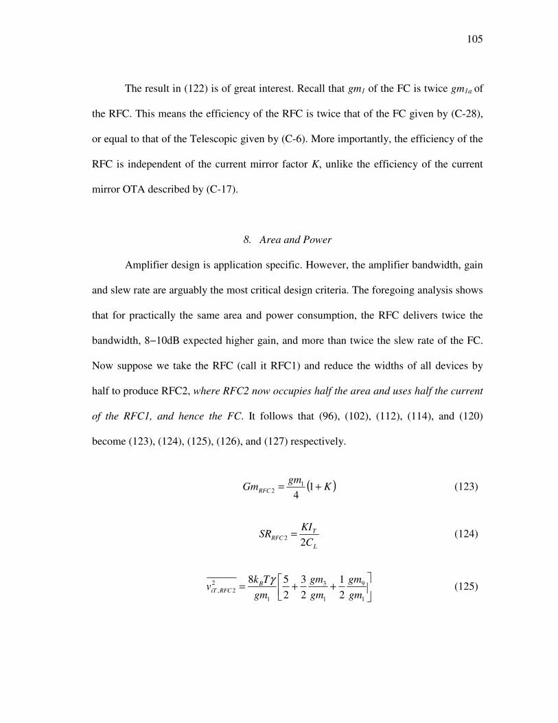
105
The result in (122) is of great interest. Recall that gm1 of the FC is twice gm1a of
the RFC. This means the efficiency of the RFC is twice that of the FC given by (C-28),
or equal to that of the Telescopic given by (C-6). More importantly, the efficiency of the
RFC is independent of the current mirror factor K, unlike the efficiency of the current
mirror OTA described by (C-17).
8. Area and Power
Amplifier design is application specific. However, the amplifier bandwidth, gain
and slew rate are arguably the most critical design criteria. The foregoing analysis shows
that for practically the same area and power consumption, the RFC delivers twice the
bandwidth, 8−10dB expected higher gain, and more than twice the slew rate of the FC.
Now suppose we take the RFC (call it RFC1) and reduce the widths of all devices by
half to produce RFC2, where RFC2 now occupies half the area and uses half the current
of the RFC1, and hence the FC. It follows that (96), (102), (112), (114), and (120)
become (123), (124), (125), (126), and (127) respectively.
( )Kgm
GmRFC += 14
12 (123)
L
TRFC
C
KISR
22 = (124)
++
=
1
9
1
3
1
2
2,2
1
2
3
2
58
gm
gm
gm
gm
gm
Tkv B
RFCiT
γ (125)

106
+
+=
2
9
1
2
3
1
11
2
2
2,2
13
2
5
L
L
L
L
K
K
fLWC
Kv
FP
FN
oxP
FPRFCif
µ (126)
( )
+
+
=
2
9
1
2
3
1
2
11
2
2,
2
2
13
2
52
L
L
L
L
A
A
LW
AV
TP
TNTP
V
V
P
NV
RFCOSµ
µσ (127)
Examining (123) shows the RFC2 to have the same transconductance as the FC,
whereas (124) shows the RFC2 still has a better slew rate than the FC. Equations (125)-
(127), however, demonstrate a degradation in noise and input offset compared to RFC1,
and hence FC.
C. Characterization
To validate the theoretical results, a FC amplifier was designed as a benchmark
in a mainstream 0.18µm CMOS process using core devices. The design procedure
followed proven analog design practices; a large input pair in weak/moderate inversion
to maximize bandwidth and minimize noise and offset, and current mirror devices with
long channels biased in strong inversion to improve accuracy and output impedance. The
main constraint applied to the design is a power budget of 800µA. Once the FC design
was finalized, RFC1 and RFC2 were derived as outlined in Sections A and B.8.
A single-ended version of the amplifiers was used in the setup of Fig. 52 to
simplify the characterization. To preserve the high output impedance and limit the DC
output current drawn, R was set to be 560kΩ. As for C1 and C2 they were set to 2.2pF
and 2.5pF respectively, which yields an overall load of 3.6pF.
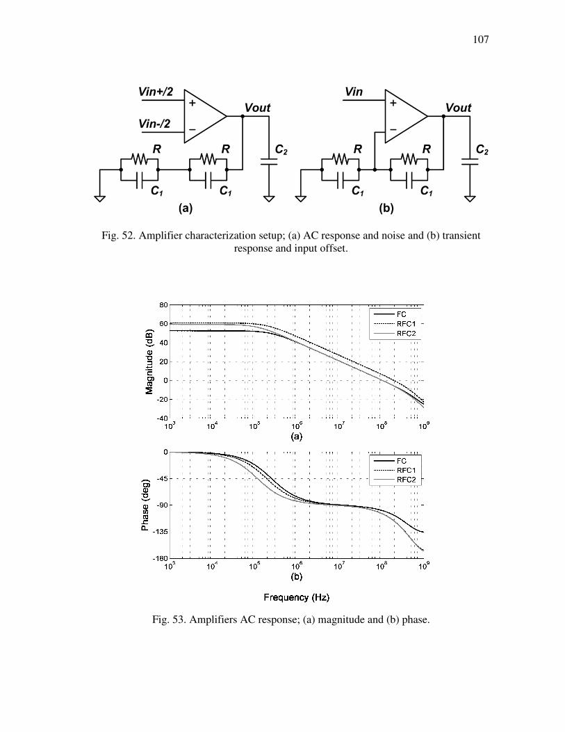
107
Fig. 52. Amplifier characterization setup; (a) AC response and noise and (b) transient
response and input offset.
Fig. 53. Amplifiers AC response; (a) magnitude and (b) phase.

108
As seen in Fig. 53, RFC1 indeed has a wider bandwidth and higher gain than the
FC, whereas RFC2 has virtually the same bandwidth, but higher gain than the FC. The
higher gain of RFC2 is not surprising; while RFC1 has +6dB gain due to an enhanced
Gm, RFC2 has +6dB gain because it consumes half the current—the additional ~3dB
improvement is attributed to M2a and M4a as explained in Section B.2.
On the other hand, the phase response shows some degradation for both RFC1
and RFC2 with respect to the FC. This is to be expected. As discussed earlier, the
addition of current mirrors in the signal path (M3a:M3b-M4a:M4b) introduces additional
pole-zero pairs. However, these pole-zero pairs are for an NMOS low gain current
mirror, which are at high frequencies. Moreover, by satisfying the condition set by (101)
for the upper limit of K, the degradation in the phase margin should not significantly
affect the transient response of the amplifiers; here the phase margins of the FC, RFC1
and RFC2 are 80.6°, 62.5° and 75.1° respectively.
For the transient response shown in Fig. 54, the input signal was a 500mVpp
10MHz pulse with a common mode level of 450mV. This results in an output of 1Vpp
centered at 900mV (VDD/2) using the configuration in Fig. 52(b). Undoubtedly, RFC1
has a superior slew rate performance than FC as seen in Fig. 54(a). RFC2 too has a better
slew rate performance, which is seen more clearly in Fig. 54(b) as a higher peak output
current. Moreover, the settling behavior of both RFC1 and RFC2 was not affected by the
phase margin degradation in comparison to FC.

109
Fig. 54. Amplifiers transient response; (a) output voltage and (b) total output current.
The input offset was measured by applying a 450mV DC input and observing the
output in a Monte Carlo simulation. The offset was extracted using (128), where βFB is
the feedback factor and A is the amplifier’s DC gain, and used to create Fig. 55. While
the offset standard deviation is similar for both FC and RFC1, it is larger for RFC2 as
demonstrated by (127). Also, a non-zero mean is observed in Fig. 55 due to systematic
offset, not random process variations. This systematic offset has two components. First,
there is a finite current drawn by the load (2R), which causes an imbalance in the

110
currents of the output devices. Second, the feedback network sets the output to 900mV,
while ideally Vout should follow the gate voltage of M9; in the single-ended version of
the amplifiers, M9 in Fig. 49 and Fig. 50 is diode connected to bias M10. This systematic
offset is more evident in FC because of the lower DC gain.
VinA
VoutV FBOS −
+=
1β (128)
Fig. 55. Input offset distributions; (a) conventional folded cascode, (b) recycling folded
cascode 1 and (c) recycling folded cascode 2.

111
As for noise, Fig. 56 shows the PSD of the input referred noise for the FC, RFC1
and RFC2 over the bandwidth 1Hz–100MHz. Note how the flicker noise dominates the
noise performance of advanced CMOS technologies as discussed in Chapter IV. From
Fig. 56 we can see how the RFC1 has a better noise performance than the FC, and RFC2
clearly has a worse noise performance as predicted by (125) and (126).
Fig. 56. Input referred noise power spectral density.
A summary of the discussed results is shown in Table 4. In addition, the 0.1%
settling time is also included to demonstrate that indeed the modifications proposed to
the FC amplifier do enhance the overall general performance.

112
TABLE 4
AMPLIFIER CHARACTERIZATION RESULTS
Parameter FC RFC1 RFC2
Power [µA] 796 782 394
DC Gain [dB] 52.63 60.91 59.32
GBW [MHz] 106.3 197.2 105.9
Phase Margin [deg] 80.6 62.5 75.1
Capacitive Load [pF] 3.6 3.6 3.6
Slew Rate (average) [V/µs] 99.3 231.1 116.5
0.1% Settling Time [ns] 21.7 11.6 21.7
Input Offset (3σ) [mV] 7.917 7.635 11.079
Input Noise (1Hz-100MHz) [µVrms] 53.16 48.48 69.71
D. The Parameter K
Thus far, the analysis and results have been for a single value of K, which was
chosen to be 3. This choice was solely made to minimize device changes and keep the
area and power consumption of the RFC1 equal to the FC, and hence served as a good
example for comparison. However, K can take any value greater than 1. The choice of K
is design specific, and hence is left to the designer’s judgment. Nonetheless, here are
some guidelines.

113
By steadily increasing K we get a:
Larger transconductance
Higher slew rate
Degrading phase margin (best phase margin achieved at K = 1)
Degrading noise performance (minimum noise achieved at K = 1)
Degrading offset performance (minimum offset achieved at K =1)
E. Conclusions
It has been demonstrated, both in theory and simulation results, that the proposed
modifications to the conventional folded cascode, using the same area and power
budgets, can boost the gain, bandwidth and slew rate without affecting the noise
performance or introducing excess offset. On the other hand, by using half the area and
half the power budgets of the conventional folded cascode, the proposed amplifier is still
capable of delivering the same or even better dynamic performance, but on the expense
of a 1.7dB noise increase and up to 40% added offset.

114
CHAPTER VI
COMMON MODE FEEDBACK*
The use of fully-differential amplifiers has several advantages over their single-
ended counterparts; an increased output signal range, a better phase response and high
tolerance to common mode noise are a few examples. Unlike single-ended amplifiers,
however, their output common mode (CM) level—the level about which the signal
alternates—is not well defined.
Fig. 57. The differential pair amplifier; (a) single-ended and (b) fully-differential.
Consider the single-ended amplifier in Fig. 36(a), and suppose an external
feedback network is designed to set the input terminals at VICM and the output at VOCM.
* Part of the data reported in this chapter is reprinted with permission from “Optimization of direct auto-
zeroing offset cancellation in low voltage applications using dual level CMFB,” by R. Assaad and J. Silva-
Martinez, 2009. Electronics Letters, vol. 45, no. 16, pp. 809-811, Copyright 2009 by IET.
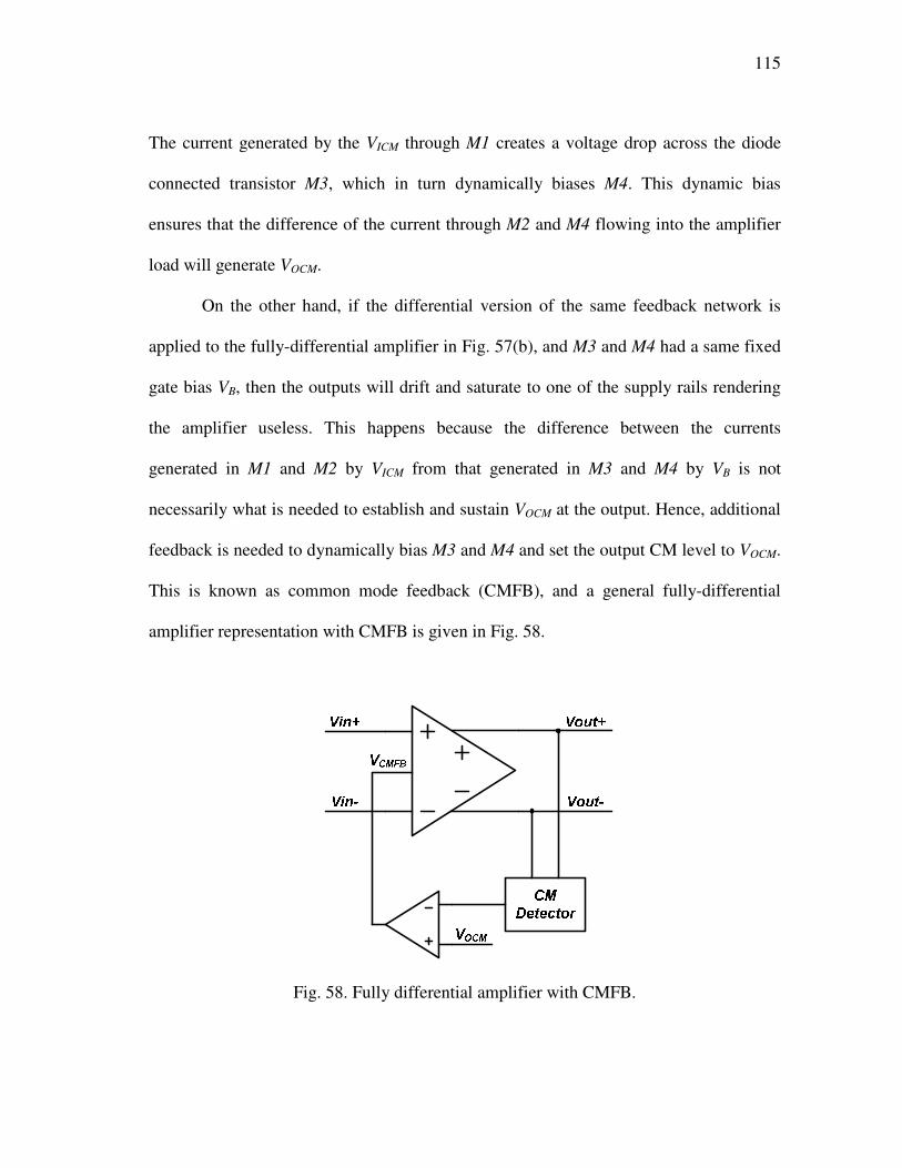
115
The current generated by the VICM through M1 creates a voltage drop across the diode
connected transistor M3, which in turn dynamically biases M4. This dynamic bias
ensures that the difference of the current through M2 and M4 flowing into the amplifier
load will generate VOCM.
On the other hand, if the differential version of the same feedback network is
applied to the fully-differential amplifier in Fig. 57(b), and M3 and M4 had a same fixed
gate bias VB, then the outputs will drift and saturate to one of the supply rails rendering
the amplifier useless. This happens because the difference between the currents
generated in M1 and M2 by VICM from that generated in M3 and M4 by VB is not
necessarily what is needed to establish and sustain VOCM at the output. Hence, additional
feedback is needed to dynamically bias M3 and M4 and set the output CM level to VOCM.
This is known as common mode feedback (CMFB), and a general fully-differential
amplifier representation with CMFB is given in Fig. 58.
Fig. 58. Fully differential amplifier with CMFB.

116
In Fig. 58, a CM detector is used to extract the CM level of the output, which
given its differential nature is a simple averaging process. In order to capitalize on the
output signal headroom of fully-differential amplifiers, the output CM is generally
centered between the supply rails, especially in low voltage applications. This is
achieved by a comparison with VOCM where the outcome is fed back to the amplifier to
adjust its bias levels; in the case of the amplifier in Fig. 57(b), VCMFB replaces the bias VB
of M3 and M4 so that their currents adjust to match those of M1 and M2 and set VOCM as
the CM output.
A. Continuous Time vs. Switched Capacitor CMFB
CMFB implementations can be classified under two main categories, continuous
time and SC. Generally, a SC CMFB is favored in a SC system such as a pipeline ADC
since the clock phases necessary for its operation are preexistent. However, the preferred
choice of SC CMFB is not just based on mere convenience. Continuous time CMFB is
based on transistors which increase the power budget, and often use current mirrors
which introduce extra poles in the CMFB loop that effectively reduce its bandwidth and
stability [81]-[82]. These shortcomings are mostly alleviated in SC CMFB.
B. Switched Capacitor CMFB
The most commonly used SC CMFB implementation is presented in Fig. 59 [83].
In this implementation capacitors C2 perform the CM detection by simply averaging the
output voltage. As for the comparison with VOCM as seen in Fig. 58 it is performed in two

117
phases. During Φ1 capacitors C1 are pre-charged to the difference of the desired output
CM level VOCM and the ideal voltage VREF needed to bias the current sources/sinks in the
amplifier to achieve the desired level. In Φ2 the charge of C1 is shared with C2 such that
the voltage across C2 becomes VOCM - VREF. Should the average of Vout+ and Vout- be
different than VOCM by some δ, then VCMFB is shifted by the same δ from VREF which
represents a unity gain comparison. This repeats over a few cycles where eventually δ
approaches 0 if the common mode loop gain is sufficiently large.
Φ1Φ1 Φ2Φ2
C1C2C2C1
Vout+ Vout-
VOCMVOCM
VREFVREF VCMFB
CP
Fig. 59. Classical switched capacitor CMFB circuit.
There are some considerations necessary for an efficient implementation of a SC
CMFB. Primarily, we consider the CMFB loop bandwidth. The capacitors C2 increase
the differential mode (DM) load and therefore should be minimized so as not to
significantly slow down the amplifier. However, as VCMFB biases the gate of a current
source/sink, there is a finite parasitic capacitance CP at that node. CP along with C2
determine the high frequency feedback factor β of the CMFB loop where β = 2C2 /(2C2
+ CP). To maximize the CMFB loop bandwidth, β needs to be maximized which creates

118
a trade-off between the DM bandwidth and CMFB loop bandwidth. Fortunately, while it
is beneficial to have a fast CMFB loop, it is not necessary for it to be comparable to the
differential mode (DM) loop. This is because CM disturbances are generally small and
the accuracy at which the CM is set can be an order of magnitude lower than that needed
by the DM. Additional considerations pertaining to the time needed to reach stead-state
and the absolute steady-state conditions are detailed in [84].
C. Dual Level CMFB
The direct auto-zeroing technique [41] presented in Chapter III is a reliable and
power conscious method to eliminate the low frequency disturbances and amplifier DC
offset in applications where the amplifier is reset in one of the clock phases. Some
examples of circuits using the direct auto-zeroing technique to reduce amplifier offset
are the S/H and MDAC shown in Fig. 60, which are extensively used in pipeline ADCs.
The output of the S/H and MDAC during Φ2 are given by (129) and (130) respectively,
where VOS is the amplifier offset, M is the effective number of bits resolved in the
pipeline stage and βΦ2 is the amplifier feedback factor during Φ2. Hence the output is
virtually offset free for a sufficiently high open loop gain, A.
( ) A
A
A
VVV OS
INSHOUT,+
=+
+=1
,1
11
1 αα
α (129)
( ) A
A
A
VVV OS
M
IN
M
MDACOUT,
2
22
22
1,
1
22
Φ
Φ
β
βα
αα
+=
++= (130)

119
Fig. 60. Direct auto-zeroing offset cancellation in (a) flip-around S/H and (b) pipeline
stage MDAC.
In low voltage applications, however, amplifiers are designed such that VDD is in
the order of VGS+2VGST, which forces the input and output CM, VICM and VOCM, to be
different as illustrated in Fig. 61 for a folded cascode, and prohibits the use of direct
auto-zeroing. Hence, current low voltage examples of pipeline ADCs [85]-[87] rely
solely on digital correction to overcome the amplifier input offset, which translates to a
comparator offset in the next stage. Instead of resetting the amplifier during Ф1, the input
and output terminals are shorted to the appropriate VICM and VOCM so the amplifier is
properly biased during Ф2. The offset then appears at the output without reduction—the
term (1+A) is eliminated from (129) and (130)—and is most severe for the MDAC

120
where in fact it is amplified; a 10mV input offset in a 2.5bits/stage pipeline stage MDAC
is seen as 40mV at the output and leaves little room for comparator offsets to be
corrected. As it is quite common for non-calibrated pipeline ADCs to utilize high
resolution stages at the beginning of the pipeline to overcome capacitor mismatch, offset
cancellation becomes necessary. In this dissertation, a dual level CMFB is presented to
alleviate this issue.
Fig. 61. Different input and output CM in a low voltage folded cascode amplifier.
In Fig. 62(a) an improved implementation [88] of the classical SC CMFB is
shown, which has the advantage of balancing the load in applications where the
amplifier is used in both clock phases. The drawback, however, is the added switches
and capacitors. By removing C2 and introducing two CM levels, VICM and VOCM, a dual
level CMFB is achieved and is shown in Fig. 62(b). The operation of the dual level
CMFB is as follows. During Ф1 the output CM is set to VICM. Thus by resetting the

121
amplifier as in Fig. 60, the offset is sampled and the amplifier is biased properly in
preparation for Ф2. During Ф2 the output CM is switched to VOCM to maximize the
output swing. Hence, direct auto-zeroing is reinstated to actively cancel the offset,
despite the different input and output CM of low voltage applications.
Fig. 62. Switched capacitor CMFB circuits; (a) improved classical circuit and (b) dual
level CMFB.
Such dynamic change in the CM output is simulated in TSMC 0.18µm CMOS
for the fully-differential implementation of the S/H shown in Fig. 60(a), using the
recycling folded cascode amplifier with gain boosting and a supply of 1.2V at sampling
rate of 100MS/s. The S/H has a total single-ended capacitive load of 1.4pF. The

122
waveforms in Fig. 63 show the change in VCMFB and output CM for each clock phase;
VICM is around 300mV to optimize the biasing of a PMOS driver, and VOCM is 600mV to
maximize the output swing.
Fig. 63. Dynamic change in output common mode using a dual level CMFB circuit; (a)
VCMFB and (b) output CM.
For the CM step of 300mV shown here, the amplifier can completely switch CM
levels in less than 2ns within 1% accuracy. An input differential offset of 50mV was
imposed in the schematic similar to Fig. 60(a), and Fig. 64 shows the input and sampled
output signals demonstrating effective offset sampling in the reset phase and cancellation
in the hold phase for a 500mVpp 12.6MHz signal.

123
Fig. 64. Sampled signal in a flip-around SHA showing 50mV sampled offset and offset
free held output.
D. Design Concerns of Dual Level CMFB
Similar to the classical SC CMFB, there are some considerations with the dual
level CMFB. These considerations can be either static and thus related to the steady-state
performance, or dynamic and are best analyzed from the frequency domain perspective.
1. Static Performance
The principal function of the dual level CMFB is to change the CM output level
for each clock phase thereby enabling the use of direct auto-zeroing in low voltage
applications. When setting the output CM level to VICM, the VDS drop across the output
devices is reduced and so is the gain, which may imply a reduced efficiency in offset

124
reduction according to (129) and (130). This, however, is not a major issue for multi-
stage amplifiers as the gain is mostly provided by the first stage(s) and the last stage is
designed for rail-to-rail swing. As for single stage cascode amplifiers, gain boosting
techniques are necessary for small settling errors and can be designed to provide
sufficient gain even when the output is at VICM; a gain of only 40dB reduces an effective
output offset of 50mV down to 500µV, which has negligible impact on the accuracy of a
pipeline stage even at high bits/stage resolution.
Another concern arises from potential different amplifier offsets when the output
CM is set to VICM and VOCM. Again, multi-stage amplifiers are immune to such change,
because the last stage contributes negligible offset and isolates the output from the
previous stage, thus maintaining the same amplifier offset for both output CM values.
Single-stage amplifiers, however, may be affected. It was demonstrated in Chapter IV
that the offset contribution of cascode devices is negligible as long as the devices
directly connected to the supply rails are kept in saturation. This is further affirmed when
gain boosting is used. Therefore, as long as VICM is greater than one VGST away from the
supply rails such that the rail devices are kept in saturation, the offset of single-stage
amplifiers will be virtually the same when the CM is set to either VICM or VOCM.
2. Dynamic Performance
The cost of removing C2 (see Fig. 62) means that for the brief time of clock non-
overlap, the amplifier has no CM control. However, high sampling rates have 100-200ps
of clock non-overlap, which minimize the risk by allowing for minor CM drifts. Another

125
aspect of the removal of C2 is the loss of the direct high frequency CM path. Instead, the
finite resistance of the switches added in series with either C1a or C1b has a mild low pass
filter effect, which can be optimized with proper switch and capacitor sizing without
adversely affecting the CMFB bandwidth. Moreover, the CM feedback factor given here
by β = 2C1a,b /(2C1a,b+CP), where CP represents the parasitics at VCMFB can be optimized
to the best compromise in speed and stability.
An added benefit of a CMFB circuits is the additional CM noise reduction they
provide to fully-differential amplifiers. However, amplifiers using SC CMFB have been
demonstrated to be vulnerable to poor power supply rejection (PSR) performance, [83]
and [89], and therefore the PSR of the dual level CMFB is analyzed and compared to the
classical implementation. To begin, a fully-differential folded cascode amplifier with
CMFB circuit connections is shown in Fig. 65. The CMFB can be substituted with the
classical implementation of Fig. 59, or the dual level CMFB of Fig. 62(b). Also shown in
Fig. 65 are simple implementations of how to generate VREF, VOCM and VICM.
Fig. 65. Fully-differential folded cascode amplifier with CMFB connections.

126
For the small signal analysis, consider the simplified half-circuit model of Fig. 65
given in Fig. 66 for the classical and dual level CMFB circuits. The amplifier ACM has
M5 as input driver and shares the same load as the folded cascode. A noise source, vn, is
imposed on VDD and a portion leaks to VREF, VOCM and VICM with factors of α and γ. The
CM output noise is denoted by vocm. By conserving charge between clock phases, the
PSR of the classical and dual level CMFB circuits seen at Ф2 can be expressed by (131)
and (132) respectively. The PSR is defined here as vocm / vn, which is desired to be <<1.
Fig. 66. Half-circuit small signal model of CMFB loop; (a) classical CMFB,
and (b) dual level CMFB.
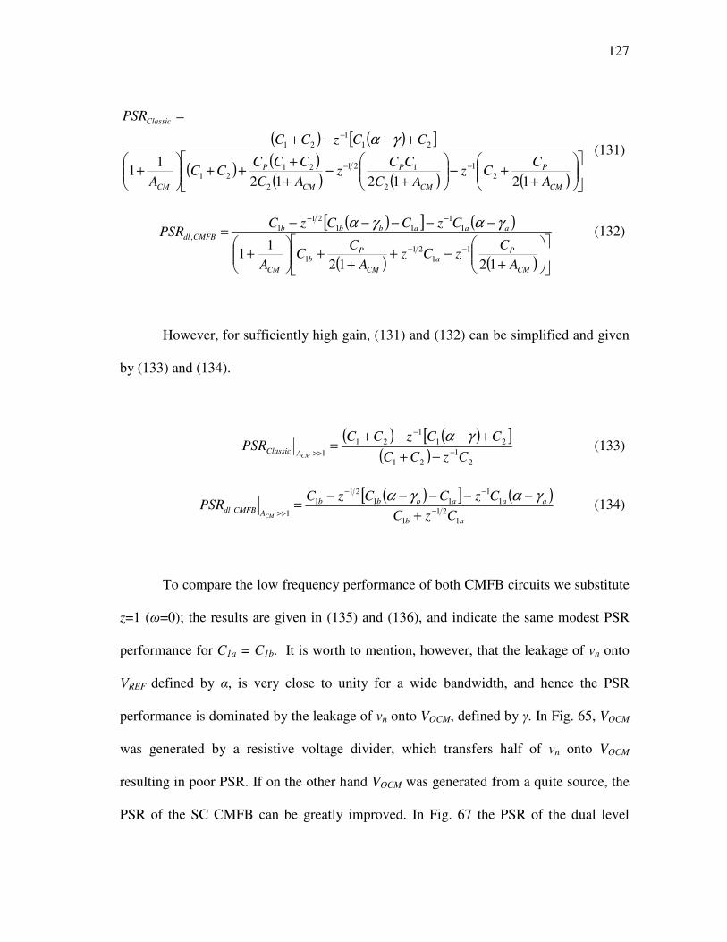
127
( ) ( )[ ]
( ) ( )( ) ( ) ( )
++−
+−
+
+++
+
+−−+
=
−−
−
CM
P
CM
P
CM
P
CM
Classic
A
CCz
AC
CCz
AC
CCCCC
A
CCzCC
PSR
121212
11 2
1
2
121
2
2121
21
1
21 γα (131)
( )[ ] ( )
( ) ( )
+−+
++
+
−−−−−=
−−
−−
CM
Pa
CM
Pb
CM
aaabbbCMFBdl
A
CzCz
A
CC
A
CzCCzCPSR
1212
11 1
1
21
1
1
1
11
21
1,
γαγα (132)
However, for sufficiently high gain, (131) and (132) can be simplified and given
by (133) and (134).
( ) ( )[ ]
( ) 2
1
21
21
1
21
1 CzCC
CCzCCPSR
CMAClassic −
−
>> −+
+−−+=
γα (133)
( )[ ] ( )
ab
aaabbb
ACMFBdlCzC
CzCCzCPSR
CM1
21
1
1
1
11
21
1
1, −
−−
>> +
−−−−−=
γαγα (134)
To compare the low frequency performance of both CMFB circuits we substitute
z=1 (ω=0); the results are given in (135) and (136), and indicate the same modest PSR
performance for C1a = C1b. It is worth to mention, however, that the leakage of vn onto
VREF defined by α, is very close to unity for a wide bandwidth, and hence the PSR
performance is dominated by the leakage of vn onto VOCM, defined by γ. In Fig. 65, VOCM
was generated by a resistive voltage divider, which transfers half of vn onto VOCM
resulting in poor PSR. If on the other hand VOCM was generated from a quite source, the
PSR of the SC CMFB can be greatly improved. In Fig. 67 the PSR of the dual level
128
CMFB was simulated using transient periodic steady state analysis; Fig. 67(a) shows α,
γa and γb versus frequency up to fS/2, and Fig. 67(b) shows the PSR of different noise
combinations onto VICM and VOCM for C1a = C1b. Clearly, a quite VICM and VOCM can
significantly improve the PSR performance.
γαω
+−=→
10ClassicPSR (135)
( ) ( )
ab
aabbCMFBdl
CC
CCPSR
11
11
0,
11
+
+−++−=
→
γαγαω
(136)
Fig. 67. Effects of supply noise components on the PSR of the dual level CMFB.

129
As for the high frequency PSR performance, the parasitics and the reduced
amplifier gain will have an impact. The high frequency PSR can be found by substituting
z = -1 (ω=∞) in (131) and (132) once all powers of z have been changed to positive
integers. The results are given by (137) and (138) respectively. Note that both CMFB
circuits have again almost the same performance where γα −+1 approaches unity at
high frequencies in agreement with Fig. 67; γ approaches unity because of the
deglitching capacitor CD in Fig. 65.
( )
++
+
+−=
∞→
CM
P
CM
Classic
AC
CC
A
PSR
11
11
1
2
1
γαω
(137)
( ) ( )
( )
+
−+≅
−
+
−+−−+=
∞→
CM
ba
ab
CM
aabb
CMFBdl
ACC
A
CCPSR
11
1
11
11 ,
11
11,
γαγαγαω
(138)
E. Conclusions
The presented dual level CMFB aids the robust implementation of direct auto-
zeroing offset cancellation techniques under low voltage conditions, and its effectiveness
has been demonstrated with a S/H example. The static errors of the dual level CMFB are
negligible so long as sufficient amplifier gain is maintained. As for the dynamic
performance, speed optimization techniques were discussed, and the PSR was analyzed
and shown to be similar to that of the classical CMFB.

130
CHAPTER VII
COMPARATORS
Comparators are functional blocks in many analog circuits, particularly pipeline
ADCs. In Chapter III, it was demonstrated that the sub-ADC block of a pipeline cell is
predominately based on a group of comparators with a handful of supplemental logic
gates. In this chapter we discuss the circuit implementation of comparators with a focus
on their uses in pipeline ADCs.
A. Comparator Architectures
The main function of a comparator is to amplify the difference between two
signals to a level large enough to be detected by subsequent digital circuitry in a very
short time. The first architectural difference among comparators is the input signal type,
which can be either voltage or current in nature, but in the case of pipeline ADCs voltage
comparators are the most widely used. Another architectural difference is the method by
which the input difference is amplified to reach logic values, which classifies
comparators into amplifier-type or latch-type.
1. Amplifier-Type Comparators
Amplifiers are most commonly used in a closed loop configuration, but if used in
open loop can also function as comparators. However, amplifier-type comparators
seldom find use in high speed applications. First, the amplifier gain is strongly related to

131
its output swing, which degrades significantly near rail-to-rail operation necessary to
drive subsequent digital circuits; this may require cascading of several amplifiers to
achieve the necessary gain, thereby needlessly increasing the complexity, area and
power consumption of the comparator. Second, the amplifier is ultimately limited by its
slew rate in charging/discharging its load; to achieve a faster rail-to-rail transition will
generally dictate a higher bias current. Therefore, amplifier-type comparators are rarely
seen in practical application, apart from slow and low cost designs [90].
2. Latch-Type Comparators
At the heart of a latch-type comparator is a pair of back-to-back inverters—a
latch—from which this comparator type gets its name. Latch-type comparators are
generally faster than amplifier-type comparators due to the positive feedback loop of the
latch. To briefly examine how a latch-type comparator functions, consider the
conceptual schematic in Fig. 68(a). Focusing on the latch alone, and assuming the
following small-signal parameters for the inverters: transconductance gmLatch,
conductance gO,Latch and output capacitance CLatch, we can write the following KCL
equations at the output of each inverter.
0, =++dt
dVCVgVgm A
LatchALatchOALatch (139)
0, =++dt
dVCVgVgm A
LatchALatchOALatch (140)

132
Equations (139) and (140) can be combined as seen in (141), where
AA VVV −=∆ . When integrated, (141) results in (142) where τLatch represents the latch
time constant. Therefore, to enhance the speed of the latch, one needs to minimize the
load capacitance at the nodes AV and A
V and maximize the transconductance of the
inverters; with proper design, decision times in the order of 100s of pico seconds can be
achieved.
( ) 0, =−−dt
dVCVggm LatchLatchOLatch
∆∆ (141)
( )( )
( ) LatchLatch
LatchOLatch tt
C
ggm
eVeVVτ
∆∆∆ 00
,
==
−
(142)
Fig. 68. Latch-type comparator; (a) conceptual schematic and (b) time-domain
waveforms.
The exponential behavior of the latch described by (142) is triggered by the input
pair M1 and M2; according to the values of V1 and V2, a small differential current is

133
generated which causes an imbalance in the charge held by the output capacitance at AV
and A
V thus triggering the exponential behavior of the latch. The resulting time-domain
waveforms of AV and A
V are shown in Fig. 68(b); beginning at some initial value VA(0),
AV and A
V start drifting exponentially towards opposite supply rails. This exponential
behavior eventually dampens as the inverters saturate at either rail due to the
conductance gO,Latch increasing and transconductance gmLatch diminishing. Once the latch
reaches a stable condition, it will retain that state until reset for a new comparison to take
place. Therefore, latch-type comparators are naturally clocked comparators and are
commonly followed by an SR latch to preserve their output after reset for post
processing while waiting for a new comparison event to take place.
Because of their high speed operation and fairly low power consumption, latch-
type comparators are preferred over amplifier-type comparators, and are extensively
used in ADCs, particularly in Pipeline and Flash ADCs. The following sections are
devoted to the sub-division of latch-type comparators: Static and Dynamic.
B. Static Comparators
Static comparators continually conduct a fixed and known bias current regardless
of the comparator state; reset or latched. There are several topologies that fall under this
category, and are easily classified as class A or class AB output similar to the
comparator architectures of Fig. 69.

134
1. Class A Output
First, let us consider the class A output comparator in Fig. 69(a) [91]-[93]. When
VLatch is HIGH, M1-M4 pre-amplify the difference VIP - VIN and the result is injected as a
differential current via M5-M6 and triggers the latch M7-M8. When VLatch goes LOW, S1
and S2 pull the comparator outputs to VDD, while S3 blocks the current path in the latch.
Hence, during either phase the steady state current flowing through the comparator is IB.
This topology is fairly fast and can achieve a low input offset by optimizing the
operating points and dimensions of M1-M4. A simpler class A output comparator
topology can be implemented by feeding the output of M1-M2 directly into a PMOS
cross-coupled load. However, this approach eliminates the preamplifier and thus makes
the comparator slower and more vulnerable to kickback noise as will be demonstrated in
later sections.
Fig. 69. Static latch-type comparators; (a) class A and (b) class AB output.

135
2. Class AB Output
Now we consider the class AB output comparator in Fig. 69(b) [94]-[98]. When
VLatch is HIGH, M1-M2 convert the difference VIP - VIN into current, which is directly
injected into the output nodes thereby triggering the latch M3-M6. Here, and unlike Fig.
69(a), the latch is implemented in a true push-pull manner and hence is class AB output.
When VLatch goes LOW, S1 shorts the output nodes, while S2 blocks the current path in
the latch. The outputs finally settle at roughly VDD - VT(3,4). For low voltage applications,
this may not be large enough to be considered logic HIGH, and therefore a reset
mechanism similar to that of Fig. 69(a) may be used. As for the power consumption, and
similar to the class A output comparator, the steady state current during either phase
flowing through the comparator of Fig. 69(b) is IB.
An advantage of the class AB output over the class A is the shorter regeneration
time in the latch due to a larger transconductance—(gm3 + gm5) for class AB vs. gm7
only for class A output—which makes it a faster comparator. However, class AB output
comparators may suffer worse input referred offset than class A due to the larger latch
transconductance. Nonetheless, because pipeline cells use digital redundancy as in the
1.5bits/stage, they are fairly immune to comparator offsets, which makes class AB
output comparators the more attractive choice.
C. Dynamic Comparators
The principal drawback of static comparators is the constant use of power
regardless of the comparator being latched or reset. While the power consumed per

136
comparator could be small, pipeline ADCs may have +20 comparators whose total
power may amount to a significant value. Dynamic comparators aim to resolve this
inefficiency by consuming power only when needed, and like static comparators there
are several variants of dynamic comparators, but virtually all have the same basic core as
either architecture of Fig. 70 [99]-[101].
VLatch VLatch
VIP VIN
VOPVON
VDD
GND
M1 M2
M3 M4
M5 M6
S3 S4
S1 S2
VL
atc
h
VIP VIN
VOPVON
VDD
GND
M1 M2
M3 M4
M5 M6S3 S2
VLatch S3
(a) (b)
S1
VL
atc
h
S4
Fig. 70. Dynamic latch-type comparators; (a) resistive and (b) differential pair input.
1. Resistive Divider Input
We begin by analyzing the operation of the resistive divider dynamic comparator
in Fig. 70(a). When VLatch is LOW, S1 and S2 pull the comparator outputs and thus the
gates of M3-M6 to VDD, while S3 and S4 ensures that VDS(1-4) = 0, and hence VGS(3,4) =
VDD. Note that in this operation mode, the comparator conducts no current. As VLatch
goes HIGH, S1 and S2 release the gates of M3-6 while S3 and S4 pull the drains of M3
and M4 towards VDD. At this stage, M3 and M4 enter saturation mode. However, M1 and

137
M2 are operating in triode and act as voltage controlled resistors. Assuming that M3-M6
are all well-matched, the imbalance of the voltage drop across the rds of M1 and M2 is
amplified by M3 and M4 thereby triggering the latch.
Once the regeneration is complete, one of the comparator outputs is held at VDD
while the other is at GND, and the comparator conducts no current. If the VLatch signal
had a 50% duty cycle, then the comparator conducts current no more than 50% of the
time, which is a significant reduction in power consumption compared to the static latch-
type comparators. Naturally, however, the sizing of the devices will dictate the current
conducted when the comparator is in the regeneration phase and needs to be limited.
As for its input referred offset, the resistive divider dynamic comparator
performance is modest at best. Transistors operating in triode are poorly matched as they
are very sensitive to VDS and process variations. Moreover, triode devices M1 and M2
have very small gain—near or smaller than unity—which may amplify any mismatch in
M3 and M4 when referred to the input. Nonetheless, because of the inherent digital
redundancy in pipeline cells, offsets in the order of 100mV may be tolerated for 1.5-
2.5bits/stage even in low voltage applications, making the resistive divider comparator a
viable option for its low power consumption.
2. Differential Pair Input
Now consider the differential pair dynamic comparator in Fig. 70(b), neglecting
S3 and S4. In the reset phase, when VLatch is LOW, the outputs are held at VDD and hence
M3 and M4 are configured in a diode connection, but conduct no current because S3 is

138
off. Also, and due to the diode connection, the sources of M3 and M4 and drains of M1
and M2 are held at approximately VDD - VT(3,4). The moment VLatch turns HIGH, M1-M4
are all in saturation and M1 and M2 act as a differential pair steering current to either
output according to their inputs, and triggering the latch.
Compared to the resistive divider comparator, the power consumption of the
differential pair is quite similar; both comparators consume current only in the
regeneration phase. However, the differential pair input is superior as far as input
referred offset is concerned, and its performance is comparable to that of static
comparators. This enhanced performance is primarily attributed to M1 and M2 being in
saturation when the comparator is latched. Moreover, with the inclusion of S3 and S4,
the input referred offset of the differential pair comparator is further enhanced; with S3
and S4 included, only M1 and M2 are in saturation when the comparator is latched and
hence become the sole dominant contributors to input offset. There is, however, a trade-
off for using the differential pair comparator over its resistive divider counterpart; the
resistive divider comparator has a wider input range.
D. Kickback Noise
The preceding discussion spanned the operation of several comparator
architectures and key comparator design issues such as power consumption and input
referred offset. Another aspect to be examined here, and perhaps the most critical for
high speed and low voltage comparator design, is kickback noise.
The inputs and outputs of a comparator are not perfectly isolated. Thus, the rail-

139
to-rail transients seen at the output are likely to leak back to the input of the comparator
resulting in kickback noise, which can be quite problematic depending on its magnitude
and the circuit configuration driving the comparator. In a pipeline ADC for example, the
input to a pipeline cell is applied to the comparators of the sub-ADC and sampled by the
cell’s S/H. Kickback noise generated by the comparators may corrupt the sampled value
resulting in conversion errors. This is demonstrated in Fig. 71, where A represents the
amplifier of the previous stage in the HOLD phase, with input and feedback capacitors
CI and CF respectively; CL represents the sampling capacitor of the following stage; and
Comp is a single-path representation of the comparator where the input and output are
coupled through capacitor CC.
Fig. 71. Kickback noise modeling in a pipeline cell.
Regarding the rail-to-rail transient at the comparator output as a source VI, we
can find the effects of the kickback noise coupling on the sampled value of the next
pipeline cell by evaluating VO across CL; this is expressed by (143), where
βA=CF/(CF+CI) is the feedback factor of amplifier A. The kickback noise transfer

140
function of (143) has a zero at ω = 0 and a high frequency pole ωpk given by (144).
Since the comparator is aimed to react very fast, the location of ωpk and the maximum
magnitude of the kickback noise transfer function given by (145) for which ω >> ωpk,
are of greater interest.
( )[ ]AFLCOAAA
C
I
O
CCCsggm
sC
V
V
ββ −++++=
1 (143)
( ) ( )AFLC
AA
AFLC
OAAApk
CCC
gm
CCC
ggm
β
β
β
βω
−++≅
−++
+=
11 (144)
( )AFLC
C
I
O
I
O
CCC
C
V
V
V
V
pk
βωω
−++==
>>1
max
(145)
Through the examination of the modeling results, we make two observations
regarding the reduction of kickback noise. First, ωpk coincides with the amplifier’s
bandwidth, ω-3dB. Intuitively, closed loop wide bandwidth amplifiers such as those used
in high speed pipeline ADCs force VO to behave as a low impedance node, which has a
natural tendency to dissipate kickback noise quickly. This is only true as long as the
frequency of the transients caused by kickback noise is below the amplifier’s ω-3dB,
which is maximized when βA = 1. Therefore, a possible approach to minimize kickback
noise is to design the amplifier’s time constant τA driving the comparator to be smaller
than that of the latch as expressed by (146), and in so doing maximize the amplifier’s
immunity against kickback noise.

141
( )
Latch
LatchOLatch
Latch
OAAA
AFLCA
ggm
C
ggm
CCCτ
β
βτ =
−<
+
−++=
,
1 (146)
Nevertheless, relying solely on the condition set by (146) to reduce kickback
noise may not be practical as it may require increasing the power consumption of
amplifier A. This leads to the second observation; the kickback noise magnitude is
strongly related to the value of the coupling capacitor, CC. Indeed, if CC is reduced, so
would be the kickback noise, and that is precisely what almost all kickback noise
reduction techniques aim to accomplish.
Before we discuss these techniques, however, let us take a closer look at (145).
Note that the values of CL, CF and βA are all predefined by the architecture used to
implement the pipeline cells. Also, it seems that a smaller βA, and thus a larger number
of bits per stage, would minimize the kickback noise. On the other hand, and due to
capacitor scaling, CL and CF become increasingly smaller as the number of bits per stage
increases, whereas CC remains unchanged as the same comparator architecture is
generally used throughout the ADC; this effectively increases the effects of kickback
noise in latter stages of the pipeline ADC. Moreover, a smaller βA would reduce the
amplifier’s natural ability to suppress kickback noise by lowering ωpk as expressed in
(144). Therefore, to maximize the pipeline ADC natural immunity against kickback
noise induced conversion errors, the use of smaller number of bits per stage is
encouraged, especially when an aggressive capacitor scaling approach is used.

142
1. Kickback Noise Reduction in Static Comparators
In addition to the natural approach of kickback noise reduction outside of the
comparator, some design techniques are used to physically limit the value of CC and here
we discuss the most relevant to static comparators.
First, we examine the preamplifier approach [37], [81]. The kickback noise
leakage through CC can be reduced if a preamplifier is inserted between the previous
stage amplifier and the latched comparator; this is similar to Fig. 69(a), where M1-M4
represent the preamplifier and is modeled in Fig. 72.
Fig. 72. Kickback noise modeling in a pipeline cell with a preamp driven comparator.
Naturally, deriving the kickback noise transfer function at VO is more complex
than that of Fig. 71, but from an intuitive standpoint, Cgd1 introduces another zero at ω
= 0 and gm3 introduces another low impedance node in the kickback noise path to
dissipate it. It is simple, however, to determine the maximum magnitude of the kickback
noise transfer function by evaluating the capacitive path represented in solid lines in Fig.
72; the result is given by (147).
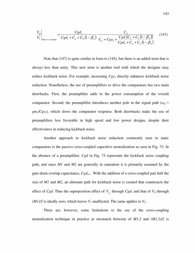
143
( ) ( )( )
( )AFL
AFLC
C
AFLpreampwI
O
CCCgd
CCCgdCgsC
C
CCCgd
Cgd
V
V
β
ββ−++
−+++
⋅−++
=
1
11
1
13
1
1
/max,
(147)
Note that (147) is quite similar in form to (145), but there is an added term that is
always less than unity. This new term is another tool with which the designer may
reduce kickback noise. For example, increasing Cgs3 directly enhances kickback noise
reduction. Nonetheless, the use of preamplifiers to drive the comparators has two main
drawbacks. First, the preamplifier adds to the power consumption of the overall
comparator. Second, the preamplifier introduces another pole in the signal path (ωp ≈
gm3/Cgs3), which slows the comparator response. Both drawbacks make the use of
preamplifiers less favorable in high speed and low power designs, despite their
effectiveness in reducing kickback noise.
Another approach to kickback noise reduction commonly seen in static
comparators is the passive cross-coupled capacitive neutralization as seen in Fig. 73. In
the absence of a preamplifier, Cgd in Fig. 73 represents the kickback noise coupling
path, and since M1 and M2 are generally in saturation it is primarily assumed by the
gate-drain overlap capacitance, Cgdov. With the addition of a cross-coupled pair half the
size of M1 and M2, an alternate path for kickback noise is created that counteracts the
effect of Cgd. Thus the superposition effect of A
V through Cgd1 and that of VA through
(M1)/2 is ideally zero, which leaves V1 unaffected. The same applies to V2.
There are, however, some limitations to the use of the cross-coupling
neutralization technique in practice as mismatch between of M1,2 and (M1,2)/2 is

144
unavoidable; physical mismatch in size is a limitation induced by process variations,
which leads to imperfect kickback noise cancellation. Moreover, saturation conditions in
short channel devices are no longer characterized by the classical channel pinch-off
where charge vanishes at the drain [56]. Therefore Cgd1,2 can be considerably different
from Cgdov provided by (M1,2)/2 creating an even greater mismatch and consequently
only modest kickback noise reduction.
V1 V2
M1 M2
Cgd1 Cgd2
IB
(M1)/2 (M2)/2
VAVA
Fig. 73. Passive cross-coupled capacitive neutralization technique.
Finally, an additional technique to reduce the effects of kickback noise is the
insertion of cascode devices inline with the differential pair of the comparator as
pictured in Fig. 74. Cascode devices are commonly used in amplifiers to enhance their
gain by limiting the output induced signal variations across the rds of the device they are
isolating. The same concept can be extended to comparators, but to isolate Cgd of M1
and M2 from the output. Thus, the effect of A
V on the drain of M1 and VA on the drain of
M2 is initially reduced by the gains of MC1 and MC2 respectively. Eventually, MC1 and
MC2 enter triode and lose their gain as VA and A
V reach the supply rails. Therefore, it is

145
crucial to ensure the bulk terminals of MC1 and MC2 are grounded and not shorted to
their sources. This guarantees a resistive path, however small, between the drains and
sources of MC1 and MC2 that impedes the propagation of kickback noise to V1 and V2.
Otherwise, CdbC1 and CdbC2 create an easy high frequency path for the kickback noise to
propagate to the inputs of the comparator.
Fig. 74. Kickback noise isolation using cascode devices.
While perhaps the most effective approach to kickback noise reduction, the use
of cascode devices shares a drawback with the preamplifier approach, and that is the
insertion of an additional pole (ωp ≈ gmC1/CgsC1) in the signal path which slows the
response of the comparator. Moreover, the use of cascode devices may be problematic as
voltage supplies continue to shrink. Nonetheless, when used together, as is the common
practice, the preceding techniques can significantly reduce the kickback noise of latch-
type static comparators.

146
2. Kickback Noise Reduction in Dynamic Comparators
The techniques described in the previous section are not strictly associated with
static comparators, but can also be used to with dynamic comparators. However, because
of the different mechanisms of operation and propagation of kickback noise in dynamic
comparators compared to their static counterparts, these techniques may not be very
effective or efficient. For example, the use of a static power consuming preamp with a
dynamic comparator is counter productive as far as power saving is concerned. This
section begins with a description of how kickback noise is generated in dynamic
comparators, followed by a presentation of a commonly used sampling-based kickback
noise reduction technique, and finally proposes a new power conscious approach to
kickback noise cancellation.
In static comparators, the primary leakage path of kickback noise was through
the gate-drain capacitance, Cgd, of the input pair M1 and M2. This is not always the case
in dynamic comparators. For instance, Fig. 75(a) shows an enlarged partial schematic of
the differential pair dynamic comparator of Fig. 70(b), including explicit representation
of the gate-drain parasitics and key waveforms. Unlike the static comparators where the
drain potentials of M1 and M2 begin at the same voltage and end at opposite supply rails,
thus generating kickback noise, the drain potentials of M1 and M2 in dynamic
comparators begin at the same voltage and end at the same supply rail, which is GND in
this case.
Hence, and from a signal perspective, it seems that Cgd1 and Cgd2 do not provide
a leakage path for kickback noise as they experience the same input step. However, what

147
is not seen in Fig. 75(a) is the dependency of Cgd1 and Cgd2 on their respective input
values, and it is this input voltage dependency that creates a path for kickback noise.
This path is strongest when the differential input is at its maximum (Cgd1 ≠ Cgd2), and
virtually nonexistent when the differential input is very small (Cgd1 ≈ Cgd2). The
resistive divider dynamic comparator is more sensitive to this kickback noise path as M1
and M2 are normally operating in triode, unlike the differential pair comparator where
M1 and M2 begin their operation in saturation; suppose a maximum differential input is
applied to the resistive divider comparator with V1 > V2, then it is likely that M2 is off
while M1 is in deep triode making Cgd1 >> Cgd2 and inducing a significant kickback
signal at the inputs.
Fig. 75. Kickback noise coupling in dynamic comparators; (a) through Cgd and (b)
through Cgs.
There is also another kickback noise path that is found in dynamic comparators
and not static comparators, and that is through Cgs1 and Cgs2. The differential pair

148
comparator is more vulnerable to this path due to the presence of a latched switch at the
sources of M1 and M2 as seen in Fig. 75(b). When VLatch is LOW, the source potential
VS1,2 of M1 and M2 is approximately at maxV1,V2 – VT(1,2). As VLatch goes HIGH, VS1,2
is pulled to GND generating a step that is fed back to the inputs through Cgs1 and Cgs2.
Similar to the kickback noise path through Cdg described earlier, this path is strongest
when the differential input is at its maximum (Cgs1 ≠ Cgs2), and virtually nonexistent
when the differential input is very small (Cgs1 ≈ Cgs2). The resistive divider comparator
can too suffer from this kickback noise path but at a much smaller scale; if the routing
parasitic to GND has a sizable resistance RGND, then the inrush current as the comparator
is latched can create a step across RGND leading to kickback noise through Cgs1 and Cgs2.
Unfortunately, none of the kickback noise reduction techniques used for static
comparators are robust against voltage-dependent capacitors. Therefore, to overcome the
effects of kickback noise in dynamic comparator, a sampling based approach is used
[102]. This is demonstrated in Fig. 76 for a sub-ADC comparator in a pipeline cell, and
the operation is based on a two-phase clock cycle synchronous with that of the pipeline
ADC. In the sampling phase, Φ1, the input and reference voltages are sampled on CIN
and CR respectively, and in the holding/latching phase, Φ2, the charge is redistributed
and applied to M1 and M2 and the comparator is latched. Any kickback noise is now
completely isolated from the inputs due to the sample and hold process. Instead, the
comparator kickback noise is dumped on CIN + CR at either input and the error is
compensated for by the digital redundancy of the pipeline cell. The only error seen at the
original inputs, Vin+ and Vin-, is the clock feed-through from the switches.
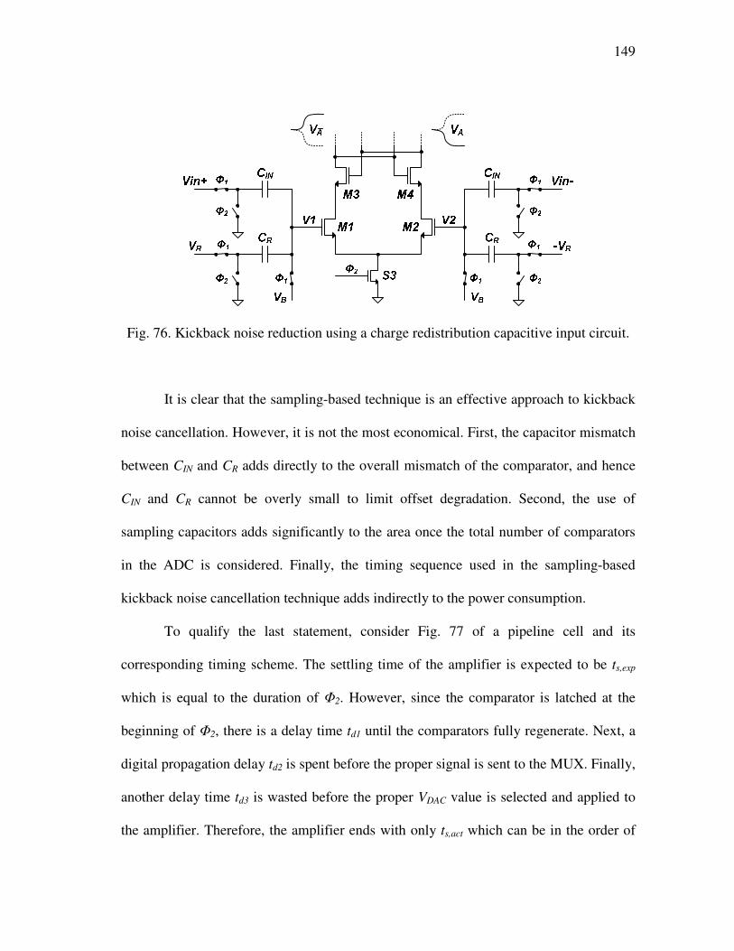
149
Fig. 76. Kickback noise reduction using a charge redistribution capacitive input circuit.
It is clear that the sampling-based technique is an effective approach to kickback
noise cancellation. However, it is not the most economical. First, the capacitor mismatch
between CIN and CR adds directly to the overall mismatch of the comparator, and hence
CIN and CR cannot be overly small to limit offset degradation. Second, the use of
sampling capacitors adds significantly to the area once the total number of comparators
in the ADC is considered. Finally, the timing sequence used in the sampling-based
kickback noise cancellation technique adds indirectly to the power consumption.
To qualify the last statement, consider Fig. 77 of a pipeline cell and its
corresponding timing scheme. The settling time of the amplifier is expected to be ts,exp
which is equal to the duration of Φ2. However, since the comparator is latched at the
beginning of Φ2, there is a delay time td1 until the comparators fully regenerate. Next, a
digital propagation delay td2 is spent before the proper signal is sent to the MUX. Finally,
another delay time td3 is wasted before the proper VDAC value is selected and applied to
the amplifier. Therefore, the amplifier ends with only ts,act which can be in the order of

150
100s of pico seconds less than ts,exp. As a result, and to achieve the required settling
accuracy in ts,act, the amplifiers need to be faster and that can only be achieved by
increasing their power budget since the loads are predefined by matching and thermal
noise requirements and cannot be reduced.
-VR
VR
VD
AC
Fig. 77. A pipeline cell and its corresponding timing and delay scheme.
In an effort to reduce the kickback noise of dynamic comparators without
excessively compromising the power and area budgets, a replica approach and a
different timing scheme are proposed, which are geared towards the differential pair
dynamic comparator. First we reexamine the timing scheme as given by Fig. 78 where
the main change from Fig. 77 is the separation of VLatch from Φ2; VLatch now goes HIGH
halfway into Φ1 and LOW synchronous to Φ1. This separation of VLatch from Φ2 provides
ample time for comparator regeneration, digital delay propagation and selection of the

151
proper VDAC before is Φ2 enabled. Thus, the amplifier indeed utilizes all of Φ2 for settling
and an increase in its power consumption for these delays as in the case of the sampling
approach is avoided.
t
Φ1
Φ2
td1
td2
Comparator
output ready
Digital delay to
MUX input
MUX delay to
VDAC ready
ts,act = ts,exp
VLatch
td3
Fig. 78. Proposed timing scheme for kickback noise reduction.
A concern may arise from the timing scheme of Fig. 78 in regard to the
comparator being latched before the MDAC of the previous pipeline stage has
completely settled at the end of Φ1. However, since the settling requirement of an
MDAC is far stringent than the input requirement of a sub-ADC, latching the
comparator halfway through Φ1 will not result in decision errors. Consider for example
the first MDAC in a 1.5bits/stage of a 10bit ADC. The error in the final settling of the
MDAC needs to be within 0.05% (½ LSB of 9+1 bits), which translates to a minimum of

152
7.6 time constants. On the other hand, due to the inherent digital redundancy of the sub-
ADC and the output being only 2bits, the accuracy of the input to the comparators needs
to be within 12.5% (½ LSB of 2 bits), which is only 2 time constants. If indeed the
comparators are latched halfway into Φ1, then the MDAC of the previous stage would
have settled to within 2.2% (3.8 time constants) and an accurate comparator decision is
guaranteed. Moreover, latching the comparators early maximizes the time for the
amplifier to naturally recover from kickback noise as discussed at the beginning of
section D.
In addition to the timing scheme, the proposed approach makes use of a
comparator replica to counteract the step seen at the sources of M1 and M2 when the
comparator is latched. This is demonstrated in Fig. 79 along with the necessary latch
signals. The replica is intended to be an exact copy of the comparator, but only sharing
the input connections. To generate the replica latch signal VRep, an inversion of VLatch and
Φ1 are passed through an AND gate. Hence, the comparator and replica are only latched
during the duration of Φ1 to save on power. Neither the rising edge of VRep nor the falling
edge of VLatch is of significance as they occur with the rising and falling edges of Φ1. The
crossing of VRep and VLatch is where the kickback noise reduction takes place.
The area increase for the replica is disadvantageous but necessary to be able to
replicate the dynamics of the kickback noise through Cgs of M1 and M2. Moreover, a
replica is only needed for the first few pipeline stages. Once the capacitor scaling of
stages is ceased and the last pipeline stage is copied down, the resolution becomes rather
coarse and the pipeline cells more tolerant to kickback noise, and thus a replica is no

153
longer necessary. Therefore, the comparator area is not doubled, but perhaps increased
by 40% if a replica is no longer used beyond the fourth pipeline stage based on a
1.5bits/stage architecture. Finally, the replica does not provide perfect cancellation as the
dynamics of the voltage-dependent capacitors are difficult to match precisely.
Nonetheless, together with the timing scheme good results can be achieved.
V1 V2M1 M2
VAVA
M3 M4
Cgs1 Cgs2
VLatch
VS1,2
S3
t
Φ1
Φ2
VLatch
VRep
Comparator Replica
V1 V2M1R M2R
M3R M4R
Cgs1R Cgs2R
VRep
VS1,2R
S3R
Fig. 79. Proposed kickback noise reduction approach including the core comparator, a
replica and the associated timing scheme.

154
E. Comparator Implementation and Simulation Results
The comparator architecture used in the pipeline ADC is based on the dynamic
differential pair input comparator and the proposed kickback noise reduction technique
discussed in the previous section. Here the focus is shifted to the implementation of the
comparator used in the pipeline ADC of this work and the simulation results.
The comparator presentation thus far was based on single ended input
comparators, but in a pipeline ADC all signals are take differential form. To convert the
comparator from single to differential input, one need only modify the differential pair
as in Fig. 80. Moreover, since the differential input pair operate in saturation when the
comparator is latched, the switching threshold of the comparators is adjusted by scaling
the dimension of M1 and M2 as expressed by (148) [99]-[101].
Fig. 80. Transformation of a single-ended input comparator to fully differential.
( )( )
( ) ( )( ) RRRININThresholdIN V
LW
LWVV
LW
LWVVV
1
2
1
2 =−=−= −+−+ (148)

155
For the following simulation results, the setup used a model for a first stage
MDAC with 90dB DC gain, 1.35GHz GBW and total capacitive load of 2.0pF to drive
the comparator differentially based on Fig. 71. The MDAC is sampling a 10MHz signal
at 200MS/s with a 1Vpp swing. The waveforms in Fig. 81 show the output of the
MDAC without a comparator; with a comparator but no kickback noise reduction; and
with a comparator and proposed kickback noise reduction.
A
A
B
B
Fig. 81. The effect of kickback noise on MDAC output.
Note how the magnitude of the kickback noise follows that of the input signal
due to the voltage-dependent capacitance that dominates the leakage path as previously
discussed. This is fairly clear from the enlarged sections where the magnitude of the
glitches is larger for larger inputs and vice versa. Also, while the proposed technique

156
does not fully eliminate the kickback noise as apparent from the presence of glitches, the
overall charge injected from the comparator and replica help bring the final settling
value closer to the ideal case. In the case of the comparator alone the final value was
715µV greater than the ideal case (0.73 LSB), whereas using the proposed kickback
noise reduction technique the final value was only 153µV (0.16 LSB) away.
As for timing, using the proposed scheme and sampling at 200MHz, the
comparator has roughly 1ns to fully regenerate. In Fig. 82, the outputs of the comparator
AV and A
V are captured along with VLatch. The worst case regeneration time occurs for
the smallest input and is typically 380ps, which leaves ample time to account for digital
circuitry and MUX delays.
380ps
1.3ns
(a)
Fig. 82. Comparator regeneration time; (a) outputs VA and A
V and (b) VLatch.

157
Finally, the greatest advantage of the dynamic comparators is their low power
consumption, and Fig. 83 shows the total transient current of the comparator including
the replica used for kickback noise reduction. Notice how the current transient is
characterized with three distinctive spikes per sampling period (5ns), which indicate the
shoot-through currents as the comparator and replica latches are activated. These spikes,
however, decay quickly as the comparator regenerates. The average power consumption
of the comparator including the replica is 120µA, which amounts for a total power of
1.8mA for the whole ADC—approximately 6.9%. This can be further improved if a
slight non-overlap is established for VLatch and VRep to drive the PMOS and NMOS
devices separately and minimize shoot-through.
Fig. 83. Comparator and replica total current; (a) control signals VLatch and VRep and (b)
total transient current.

158
In summary, through a survey of the different comparator types and analysis of
kickback noise behavior, a power conscious technique for kickback noise reduction is
proposed for dynamic differential pair input comparators. When examined with a true
MDAC, the proposed technique proved useful in reducing the error caused by kickback
noise such that the settling error is within 0.16 LSB. This is achieved through the use of a
timing scheme that allows the amplifier to capitalize on its natural kickback noise
rejection, and a replica which reduces the kickback noise by superposition of opposite
polarity signals. Moreover, the proposed technique is power efficient despite the fact that
it relies on a replica approach, as it ensures the maximum allowable settling time for the
amplifiers through the elimination of digital circuit and MUX delay intrusions into the
HOLD phase of the MDAC.

159
CHAPTER VIII
SIMULATION AND EXPERIMENTAL RESULTS
The discussion in the preceding chapters demonstrated the direct effects of the
amplifier performance on that of the pipeline ADC, and the challenges that come with
high speed, low voltage and low power design. For that purpose, a new amplifier
topology—the recycling folded cascode—was proposed that effectively addresses many
of these limitations.
In this chapter, the simulation and experimental results of the research are
presented. First, the conventional folded cascode and the recycling folded cascode are
examined. Then, a S/H amplifier suitable for a 1Vpp 10bit Pipeline ADC with up to
200MS/s, which is built on the recycling folded cascode and employing the dual level
CMFB is presented. The prototype amplifiers and the S/H were fabricated on the same
die using TSMC 0.18µm CMOS technology, and the die was packaged in a QFN40 chip.
To facilitate the testing, a PCB was designed to accommodate both test setups, and
provide easy access to multiple points in the signal path for verification. Fig. 84 shows
the bonded die in the open cavity QFN40 package, and Fig. 85 shows the PCB used in
the test. Finally, a complete low voltage, low power, 10bit, 160MS/s pipeline ADC is
discussed, highlighting the performance with respect to state-of-the-art present
implementations.

160
Fig. 84. Amplifiers and S/H prototype chip.
Fig. 85. Prototype chip characterization PCB.

161
A. Recycling Folded Cascode
The simulation results of the prototype amplifiers were presented in the
characterization section of Chapter V. Here we examine the experimental results. The
prototype amplifiers, FC, RFC1 and RFC2 were fabricated in a closed loop
configuration driving the same on-chip load, and biased with 800µA for the FC and
RFC1, and 400µA for RFC2. Fig. 86 shows the amplifiers and their respective loads as
they appear on silicon; the FC, RFC1 and RFC2 measure roughly 4700, 5000, and
3000µm2 respectively. The amplifiers configuration is shown schematically in Fig. 87
with the load and test setup. The internal load R||C1 and C2 are 560kΩ||2.16pF and 2.5pF
respectively. As for C3, it represents the total parasitic capacitance of the output PCB
trace and the oscilloscope probe.
Fig. 86. Enlarged die section showing the FC, RFC1 and RFC2 with their loads.
RC Load RC Load RC Load
Biasing
FC RFC1 RFC2
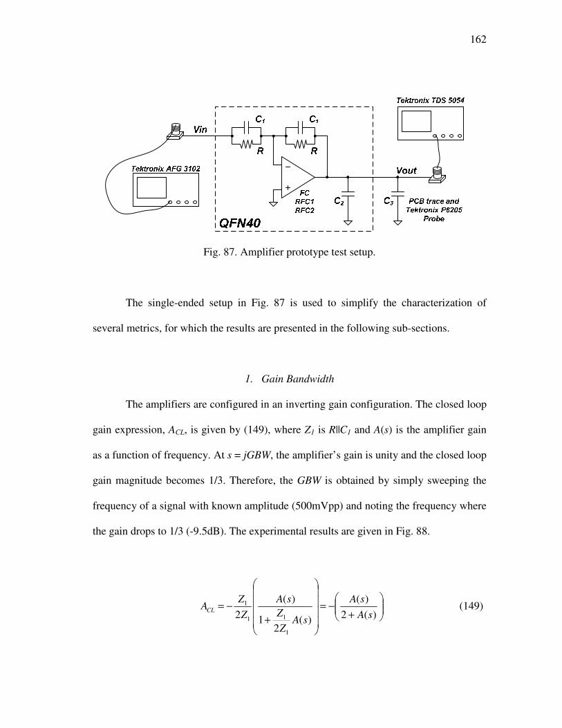
162
Fig. 87. Amplifier prototype test setup.
The single-ended setup in Fig. 87 is used to simplify the characterization of
several metrics, for which the results are presented in the following sub-sections.
1. Gain Bandwidth
The amplifiers are configured in an inverting gain configuration. The closed loop
gain expression, ACL, is given by (149), where Z1 is R||C1 and A(s) is the amplifier gain
as a function of frequency. At s = jGBW, the amplifier’s gain is unity and the closed loop
gain magnitude becomes 1/3. Therefore, the GBW is obtained by simply sweeping the
frequency of a signal with known amplitude (500mVpp) and noting the frequency where
the gain drops to 1/3 (-9.5dB). The experimental results are given in Fig. 88.
+−=
+
−=)(2
)(
)(2
1
)(
2
1
11
1
sA
sA
sAZ
Z
sA
Z
ZACL (149)

163
-15
-12
-9
-6
-3
0
3
1.E+03 1.E+04 1.E+05 1.E+06 1.E+07 1.E+08 1.E+09
Frequency (Hz)
Gain
(d
B)
FC
RFC1
RFC2
-6dB/Octave
Fig. 88. Experimental frequency sweep of FC, RFC1 and RFC2 amplifier outputs.
The first observation is that the frequency performance of the FC and RFC2 is
virtually identical despite RFC2 using only half the area and half the power of the FC.
The frequency at which the gain of the FC and RFC2 amplifiers falls to -9.5dB is
roughly 70MHz, in disagreement with the simulation results in Chapter V. This is
because in the simulations results the parasitic capacitance of the PCB traces and the
oscilloscope probes was not taken into account. By accounting for 0.25pF of PCB trace
capacitance and 2pF for the Tektronix P6205 active FET probe, the simulated load is
increased by 60%, which reduces the simulated GBW (115MHz) of the FC and RFC2 to
72MHz, in good agreement with the experimental results. As for the RFC1, the
frequency range of the Tektronix AFG 3102 was limited to 100MHz, and hence the
response was extrapolated with a -6dB/octave slope as shown in Fig. 88. Through

164
extrapolation the GBW of the RFC1 is found to be 110MHz. However, the GBW of the
RFC1 was expected to be twice that of the FC. This discrepancy is the result of the
different PCB trace capacitance seen by RFC1. Fig. 89 is a closer look at the PCB traces
associated with each amplifier and their differences. Given the width of the traces and
thickness of the PCB, the trace capacitance for the FC, RFC1 and RFC2 can be
calculated to be 0.18pF, 1.39pF and 0.24pF respectively. In addition to the 2pF input
capacitance of the Tektronix P6205 active FET probe, the overall capacitive load seen
by the FC, RFC1 and RFC2 is 5.76pF, 6.97pF and 5.82pF respectively. The difference in
trace capacitance for the FC and RFC2 is negligible when compared to the overall load
(~1%). However, the trace capacitance for the RFC1 increases the overall load by 21%.
When this is taken into account and by normalizing the GBW with respect to the FC
capacitive load, the GBW of the RFC1 becomes 133.1MHz, almost twice (1.9 times) the
GBW of the FC.
Fig. 89. PCB trace differences for the FC, RFC1 and RFC2 amplifiers.
FC
RFC
RFC
VI

165
An alternative way to measure the GBW is by applying a small step signal and
measuring the settling time. Fig. 90 shows the step response of the prototype amplifiers
to a 10MHz, 100mVpp step signal. The amplitude of 100mVpp ensures that the
amplifiers will not slew as predicted by (28). The FC and RFC2 traces are closely
overlapped indicating similar GBW, while the RFC1 clearly demonstrates a higher GBW.
The settling time of the FC, RFC1 and RFC2 to an accuracy of 1% is 20.7ns, 13.2ns and
20.8ns respectively. This translates to a GBW of 70.7MHz for the FC, 110.9MHz for
RFC1 and 70.4MHz for RFC2, in good agreement with the frequency sweep results.
Fig. 90. Small signal step response of the FC, RFC1 and RFC2 amplifiers.

166
2. Slew Rate
The amplifiers are forced to slew if the input is greater than the maximum
described by (28), which is roughly 200mV. The output response of the FC, RFC1 and
RFC2 amplifiers to a 5MHz, 1Vpp input step is shown in Fig. 91. From Fig. 91, the
RFC1 has a clearly improved SR over the FC despite the same bias current. Moreover, at
half the bias current, the SR of the RFC2 is slightly better than the FC. The average SR
of the FC, RFC1 and RFC2 normalized to the FC total capacitive load is 42.15V/µs,
94.13V/µs and 48.12V/µs respectively; that is the SR of the RFC1 is enhanced 2.23
times over the FC for the same bias current, while that of the RFC2 is enhanced 1.14
times over the FC for half the bias current.
Fig. 91. Large signal step response of the FC, RFC1 and RFC2 amplifiers.

167
3. Distortion
The linearity of the amplifiers can be measured through their distortion behavior.
A 1Vpp two tone test centered at 1MHz and separated by 100kHz (500mVpp at
0.95MHz and 500mVpp at 1.05MHz) was applied to all amplifiers and the FFT data of
the outputs was captured using the Tektronix TDS 5054 and plotted in MATLAB. The
results for the FC, RFC1 and RFC2 are given in Fig. 92. The third intermodulation
distortion, IM3, is -61.7dB for the FC, -66.1dB for RFC1 and -61.6dB for RFC2.
In Chapter IV the amplifier slew rate effects were considered for step inputs. For
continuous signals, the SR can indicate the maximum input frequency as given by (150),
where the output voltage is a time-varying signal Amcos(2πfint), with amplitude Am and
frequency fin. According to (150) and the average SR results presented earlier, the FC,
RFC1 and RFC2 amplifiers can support signals up to 13.4MHz, 29.9MHz and 15.3MHz
respectively without slewing.
( )m
ininminA
SRftfAf
t
VoutSR
πππ
22sin2
max≤⇒=
∂
∂≥ (150)
Therefore, the distortion is solely due to the reduced amplifier gain around
1MHz. The FC and RFC2 have almost identical GBWs and hence it is not surprising to
see them have similar IM3 performance, as they have the same voltage gain around
1MHz. The RFC1, on the other hand has a wider GBW and hence a higher gain around
1MHz, which explains the improved IM3 performance. According to the absolute GBW

168
results, the open loop gain at 1MHz of the FC and RFC2 amplifiers is 36.6dB and the
gain of the RFC1 amplifier is 40.8dB. The difference in gains is in good agreement with
the difference in IM3 performance for the FC, RFC1 and RFC2.
4. Summary
The overall summary of the FC, RFC1 and RFC2 performance is presented in
Table 5. Overall, if one intends to better utilize the power, RFC1 proved to be a more
efficient amplifier. It provides a higher gain, almost twice the GBW, better than twice the
average SR, a better IM3 and a lower noise and offset—all while utilizing the same
power and virtually the same silicon area. On the other hand, for half the power and
almost half the area, the same performance of the FC can be replicated using RFC2, on
the expense of an increase in noise and input offset.

169
Fig. 92. Two tone FFT spectrums of the FC, RFC1 and RFC2 for a 1Vpp signal centered
at 1MHz and separated by 100kHz.

170
TABLE 5
SIMULATION AND EXPERIMENTAL RESULTS PERFORMANCE SUMMARY OF THE FC, RFC1
AND RFC2 AMPLIFIERS
Parameter FC RFC1 RFC2
Power (µA) 800 800 400
Area (µm2)
4712.9
(53.8 x 87.6)
4958.2
(56.6 x 87.6)
3001.8
(58.4 x 51.4)
GBW (MHz) 70.7 110.9 (134.2*) 70.4
Load CL (pF) 5.76 6.97 5.82
DC Gain (dB)
46.02
(52.63**)
53.56
(60.91**)
54.89
(59.32**)
SR+ (V/µs) 42.75 65.13 (78.81*) 41.09
SR- (V/µs) 41.55
90.45
(109.44*)
55.14
Average SR (V/µs) 42.15 77.79 (94.13*) 48.12
IM3—1Vpp input
at 1MHz (dB)
-61.7 -66.1 -61.6
Input integrated noise (µVrms)
(1Hz – 100MHz)**
53.16 48.48 69.71
Input offset – 3σ (mV)** 7.92 7.64 11.08
Settling Time – 1% (ns) 20.7 13.2 (10.91*) 20.8
* Normalized to the FC capacitive load
** Simulation results

171
B. Sample and Hold
The front end of a pipeline ADC is the S/H amplifier. A flip-around S/H
architecture was designed for a 10 bit 1Vpp pipeline ADC and fabricated in TSMC
0.18µm CMOS technology as an application of the recycling folded cascode. The S/H
also utilized the low voltage two-stage gain boosting technique discussed in Chapter IV
and the dual level CMFB discussed in Chapter VI. An enlarged section of the die where
the S/H amplifier is placed is shown in Fig. 93, where CSH and CC are the sample and
hold and coupling capacitors respectively.
Fig. 93. Enlarged die section showing the S/H amplifier and open drain buffer.

172
Tektronix AFG 3102
Tektronix TDS 5054
HP 81110A
QFN40
50
50
5050
500
500
500
500
560k560k
40
100100
16.5
16.50.22µ
0.22µ
0.22µ0.22µ
0.22µ
0.22µ
3.3p
3.3p
1p
1p
Φ1
Φ1e
Φ2
Φ1e
Φ2
Φ1
Φ1
Φ1e
Φ2
Clock
Generation
1p
1p
1p
1p
32mA 32mA
Vout -
Vout +
THS4513
1.8V
5.0V
1.2V
SHA
OR
100MHz
200MHz
100
Fig. 94. S/H test setup.

173
The test setup used to characterize the S/H is given in Fig. 94, showing all
components and their values. As the testing is done at high frequencies, careful choice of
components was necessary to improve impedance matching between the equipment used
and the PCB. The single-ended input signal was converted to fully differential using the
THS4513 wideband low distortion fully differential amplifier. Also, the THS4513
configuration acts as an anti-aliasing filter, with a corner frequency of 96.5MHz. The
clock phases necessary for operation were generated on chip using a self-biased
amplifier [103] and the logic shown in Fig. 95, which in simulations guaranteed a 50%
duty cycle ±2% for different corners and temperatures up to a CLK input of 250MHz in
a 1.8V domain. The switches were implemented using NMOS low VT devices, which
eliminated the use of bootstrapping techniques. The CLK input was provided by either a
pure sinusoidal waveform from the Tektronix AFG 3102 up to 100MHz, or the HP
81110A pulse/pattern generator up to 200MHz.
Fig. 95. On-chip generation of S/H clock phases.

174
In practice the S/H will drive the input of the first pipeline stage, which is a small
capacitive load compared to the bondpad and equipment input parasitics. Therefore, to
facilitate the testing, a highly linear open drain buffer was designed to support the drive
capability. However, as the S/H and the output buffer operate from different supply
domains, AC coupling was necessary. Overall, the total capacitance seen at the output of
the S/H is 2 pF. Assuming all-linear settling, a GBW of 700MHz is necessary for the S/H
amplifier to settle to 10 bit accuracy at 200MS/s. However, taking into account that
slewing is inevitable, the S/H was designed with GBW of 0.935GHz and more than 60°
of phase margin. The simulated AC response is given in Fig. 96.
Fig. 96. S/H amplifier AC response.

175
To verify functionality, the S/H amplifier was first tested at a 100MS/s for
various input frequencies up to and beyond the Nyquist rate. For this purpose the
Tektronix AFG 3102 dual signal generator was used. This simplified the capture of the
signals on the Tektronix TDS 5054 as both signals come from the same source. Figs. 97,
98 and 99, show trace captures on the Tektronix TDS 5054 for an input of 5MHz,
50MHz and 75MHz respectively.
Fig. 97. 5MHz input and S/H output at 100MS/s.

176
Fig. 98. 50MHz input and S/H output at 100MS/s.
Fig. 99. 75MHz input and S/H output at 100MS/s.

177
The results shown in Figs. 97-99 confirm functionality of the S/H amplifier.
More specifically, the functionality of the low voltage gain boosting, the dual level
CMFB and the use of low VT devices as switched are verified. One note, however, is the
attenuated output level with respect to the input signal. By examining the signal path
from the Tektronix AFG 3102 to the Tektronix TDS 5054, the THS4513 configuration
contributes an attenuation of 0.95, the internal coupling an attenuation of 0.5, the output
buffer an attenuation of 0.92 and finally the output matching network with an attenuation
of 0.375. This results in a total attenuation of 0.164, which is in good agreement with the
results seen in Figs. 97-99.
To step up the sampling frequency to 200MS/s, the HP 81110A pulse/pattern
generator was used for CLK. For this test, the FFT function of the Tektronix TDS 5054
was used to capture the output data of the S/H amplifier and processed in MATLAB to
generate the plots. A single tone test was first performed near the Nyquist sampling limit
using a 90MHz full scale (1Vpp) input. The results are shown in Fig. 100. The spectrum
of the S/H amplifier shows an HD3 of 57.32dB. As the spectrum is clear of any other
spurs, the SFDR is also 57.32dB. As for the SNR, the noise floor seen in Fig. 100 is
dominated by the noise of the equipment used and the output buffer. Nonetheless,
assuming a 10bit noise floor, the ENOB can be calculated to give 9.03 bits. As for Fig.
101 and 102, they show the results of a two tone test with tones of 500mVpp each
centered at 90MHz and separated by 100kHz. The spectrum is clear of any spurs, apart
from the intermodulation distortion seen in Fig. 102, yielding an IM3 of 51.34dB.

178
Fig. 100. S/H output spectrum for a 1Vpp, 90MHz input sampled at 200MHz.

179
Fig. 101. S/H output spectrum for a 2 tone 1Vpp input centered at 90MHz and separated
by 100kHz, sampled at 200MHz.
Fig. 102. Expanded spectrum of Fig. 101.

180
C. Pipeline ADC
A 10bit, 1Vpp, 160MS/s pipeline ADC was designed using the techniques
presented in the previous chapters, and laid-out using SMIC 0.18µm CMOS technology.
The general architecture of the pipeline ADC and layout of the whole chip are presented
in Fig. 103 and Fig. 104 respectively. The individual building blocks in Fig. 103 are
based on those discussed in Chapter III, using the gain boosted RFC amplifier with dual
level CMFB and dynamic comparators with kickback noise reduction where applicable.
Grey and white blocks operate from 1.2V and 1.8V supplies respectively.
Fig. 103. Block diagram of pipeline ADC designed in SMIC 0.18µm CMOS technology.

181
Fig. 104. Complete pipeline ADC layout in SMIC 0. 18µm measuring 4x4mm2 and
featuring 4 separate ADCs multiplexed to the LVDS output drivers.

182
The most challenging block in the pipeline ADC is the amplifier used to
implement the MDAC of the first pipeline stage. It needs to settle within 0.1% (10bit
accuracy) in less than 2.8ns for 160MS/s at full scale input (1Vpp). For that purpose, a
1.45GHz bandwidth amplifier is designed with 55° of phase margin and Fig. 105 shows
its AC response. To demonstrate functionality of the internal blocks, a small input is
applied to the ADC and the output of the S/H, P1 and P2 stages are plotted in Fig. 106.
This shows the multiply by 2 function of the pipeline cells and the capability to handle a
1Vpp swing.
Fig. 105. First pipeline stage amplifier AC response.

183
Fig. 106. Transient simulation of pipeline ADC showing the input signal and outputs of
the S/H, P1 and P2 blocks.
Sampling at 160MS/s, a FS single tone near the Nyquist sample rate at 78MHz
was applied as an input to the pipeline ADC. The FFT plot is given in Fig. 107. The only
visible spur is that of the third harmonic, and the HD3 is 62.46dB. Also from Fig. 107,
the calculated SNDR is 57.12 which translates to an ENOB of 9.19. A figure of merit
(FoM1) used to measure the efficiency of an ADC is described by (151), which links the
ADC power P to the resolution ENOB and sampling frequency fS. The efficiency is
quantified as pJ/conversion-step. However, to incorporate the added speed advantage of
newer CMOS technologies over older ones in the comparison, a modified version of
(151) given in (152) can be used. In (152), the transit frequency fT,other of other CMOS
implementations is normalized to that of the device under test, fT,DUT. Thus, the resulting
FoM2 is more design based than technology based.

184
Fig. 107. 1k FFT ADC spectrum for fIN = 78MHz at 160MS/s.
S
ENOBf
PFoM
21 = (151)
DUTT
OtherT
S
ENOBf
f
f
PFoM
,
,
22
⋅= (152)
A comparison of the pipeline ADC presented here with recent state-of-the-art
implementations of comparable resolution in literature is summarized in Table 6.

185
TABLE 6
PERFORMANCE SUMMARY OF RECENT STATE-OF-THE-ART PIPELINE ADCS
Parameter [13] [15] [16] [19] [23] [26]
This
Work*
CMOS
Technology
0.18/0.35
µm 90nm 130nm 130nm
0.18/0.35
µm 90nm 0.18 µm
Resolution 10bits 10bits 10bits 10bits 10bits 10bits 10bits
fS [MHz] 170 200 400 100 210 205 160
Supply [V] 3.3 1.2 1.2 3 1.8 1.2 1.2
Vin [Vpp] 2 0.8 1.2 2 1.5 1 1
Power [mW] 180 55 160 72 140 40 42
Area [mm2] 0.85 1.26 4.2 0.54 1.5 1 1.1
SNDR [dB] 57.8 53.6 53.7 56.3 59.3 53.9 57.12
SFDR [dBc] 70.3 66.5 60.9 67.5 85.9 61.8 62.46
ENOB 9.31 8.61 8.63 9.06 9.56 8.66 9.19
FoM1
[pJ/Conv-Step]
1.67 0.71 1.01 1.35 0.88 0.48 0.45
FoM2
[pJ/Conv-Step]
1.67 1.97 1.82 2.43 0.88 1.35 0.45
* Simulation Results

186
From Table 6, the pipeline ADC presented in this work demonstrates the highest
potential efficiency. Considering the technology of implementation, the presented work
is twice as efficient as a similar 0.18µm CMOS implementation, but using 27% smaller
area. The presented work also shows a slightly better efficiency than similar 90nm
CMOS implementations with only 10% increase in area.

187
CHAPTER IX
CONCLUSIONS
The pipeline ADC is a popular architecture that finds use in a wide range of
applications with resolutions up to 14bits and +100MHz sampling speeds. The current
approach to its design puts a lot of emphasis on the architectural level, rather than
finding new techniques to enhance the performance on the transistor design level. In
order to propose such new techniques, a thorough study of the pipeline ADC behavior
was undertaken, highlighting the main limitations posed by the individual building
blocks. This study concludes that the majority of errors are attributed to the performance
metrics of the amplifier used in the front-end S/H and MDACs.
A Recycling Folded Cascode (RFC) amplifier was proposed as a replacement to
the conventional folded cascode to remedy or reduce many of its limitations. It has been
demonstrated, both in theory and experimental results, that the RFC can achieve twice
the gain bandwidth, 8-10 additional gain and at least twice the slew rate as the
conventional folded cascode, without adding noise, degrading offset or using additional
area or power. Moreover, the recycling folded cascode was confirmed to be robust low
voltage environments.
To tackle the amplifier offset effects, the direct auto-zeroing offset cancellation
scheme is optimized for low voltage environments using a dual level CMFB circuit, and
it was shown that amplifier differential offsets up to 50mV are effectively cancelled.
Together with the RFC, the dual level CMFB was used to implement a fully-differential

188
flip-around sample and hold amplifier driving a single-ended load of 1.4pF and using
only 2.6mA, and at 200MS/s better than 9bit linearity is achieved.
Finally the kickback noise of dynamic comparators was addressed using a power
conscious technique that replicates the noise with the opposite polarity such that the
overall effect is reduced.
Together, these techniques were used in the design of a non-calibrated 1Vpp
10bit 160MS/s pipeline ADC in SMIC 0.18µm CMOS technology. The ADC is
composed of a simple architecture; a front-end S/H, eight 1.5bits/stage pipeline cells and
a 2bit flash. The ADC uses an area of 1.1mm2 and consumes 42mW in its analog core,
and with a near Nyquist-rate full scale signal, 9.2 ENOB is achieved. Compared to recent
state-of-the-art implementations in the 100-200MS/s range, the presented ADC design
uses the least power per conversion rated at 0.45pJ/conversion-step.

189
REFERENCES
[1] R. Brewer, J. Gorbold, P. Hurrel, C. Lyden, R. Maurino, et al., “A 100dB SNR
2.5MS/s output data rate ∆Σ ADC,” ISSCC Dig. Tech. Papers, vol. 1, pp. 172-
591, Feb 2005.
[2] P. Morrow, M. Chamarro, C. Lyden, P. Ventura, A. Abo, et al., “A 0.18µm
102dB-SNR mixed CT SC audio-band ∆Σ ADC,” ISSCC Dig. Tech. Papers, vol.
1, pp. 178-592, Feb 2005.
[3] R. Schreier, N. Abaskharoun, H. Shibata, I. Mehr, S. Rose, et al., “A 375-mW
quadrature bandpass ∆Σ ADC with 8.5-MHz BW and 90-dB DR at 44MHz,”
IEEE J. Solid-State Circuits, vol. 41, no. 12, pp. 2632-2640, Dec 2006.
[4] G. Mitteregger, C. Ebner, S. Mechnig, T. Blon, C. Holuigue, et al., “A 20-mW
640-MHz CMOS continuous-time Σ∆ ADC with 20-MHz signal bandwidth, 80-
dB dynamic range and 12-bit ENOB,” IEEE J. Solid-State Circuits, vol. 41, no.
12, pp. 2641-2649, Dec 2006.
[5] T. Chang, L. Dung, J. Guo and K. Yang, “A 2.5-V 14-bit, 180-mW cascaded Σ∆
ADC for ADSL2+ application,” IEEE J. Solid-State Circuits, vol. 42, no. 11, pp.
2357-2368, Nov 2007.
[6] Y. Yang, T. Sculley and J. Abraham, “A single-die 124dB stereo audio delta-
sigma ADC with 111dB THD,” IEEE J. Solid-State Circuits, vol. 43, no. 7, pp.
1657-1665, July 2008.
[7] S. Park, Y. Palaskas and M. P. Flynn, “A 4-GS/s 4-bit flash ADC in 0.18-µm

190
CMOS,” IEEE J. Solid-State Circuits, vol. 42, no. 9, pp. 1865-1872, Sep 2007.
[8] H. Yu and M. F. Chang, “A 1-V 1.25-GS/s 8-bit self-calibrated flash ADC in 90-
nm digital CMOS,” IEEE Trans. Circuits and Systems—II: Express Briefs, vol.
55, no. 7, pp. 668-672, July 2008.
[9] A. Ismail and M. Elmasry, “A 6-bit 1.6-GS/s low-power wideband flash ADC in
0.13-µm CMOS technology,” IEEE J. Solid-State Circuits, vol. 43, no. 9, pp.
1982-1990, Sep 2008.
[10] K. Deguchi, N. Suwa, M. Ito, T. Kumamoto and T. Miki, “A 6-bit 3.5-GS/s 0.9-
V 98-mW flash ADC in 90-nm CMOS,” IEEE J. Solid-State Circuits, vol. 43,
no. 10, pp. 2303-2310, Oct 2008.
[11] Z. Wang and M. F. Chang, “A 600-MSPS 8-bit CMOS ADC using distributed
track-and-hold with complementary resistor/capacitor averaging,” IEEE Trans.
Circuits and Systems—I: Regular Papers, vol. 55, no. 11, pp. 3621-3627, Dec
2008.
[12] T. N. Andersen, B. Hernes, A. Briskemyr, F. Telsto, J. Bjornsen, et al., “A cost-
efficient high-speed 12-bit pipeline ADC in 0.18-µm digital CMOS,” IEEE J.
Solid-State Circuits, vol. 40, no. 7, pp. 1506-1513, July 2005.
[13] J. Li, G. Manganaro, M. Courcy, B. Min, L. Tomasi, et al., “A 10b 170MS/s
CMOS pipelined ADC featuring 84dB SFDR without calibration,” VLSI Circuits
Symp. Dig. Tech. Papers, pp. 226-227, 2006.
[14] K. Iizuka, H. Matsui, M. Ueda and M. Daito, “A 14-bit digitally self-calibrated
pipelined ADC with adaptive bias optimization for arbitrary speeds up to

191
40MS/s,” IEEE J. Solid-State Circuits, vol. 41, no. 4, pp. 883-890, Apr 2006.
[15] D. Kurose, T. Ito, T. Ueno, T. Yamaji and T. Itakura, “55-mW 200-MSPS 10-bit
pipeline ADC for wireless receivers,” IEEE J. Solid-State Circuits, vol. 41, no. 7,
pp. 1589-1595, July 2006.
[16] S.-C. Lee, K. Kim, J. Kwon, J. Kim and S.-H. Lee, “A 10-bit 400-MS/s 160-mW
0.13-µm CMOS dual-channel pipeline ADC without channel mismatch
calibration,” IEEE J. Solid-State Circuits, vol. 41, no. 7, pp. 1596-1605, July
2006.
[17] A. M. A. Ali, C. Dillon, R. Sneed, A. S. Morgan, S. Bradsley, et al, “ A 14-bit
125 MS/s IF/RF sampling pipeline ADC with 100dB SFDR and 50 fs jitter,”
IEEE J. Solid-State Circuits, vol. 41, no. 8, pp. 1846-1855, Aug 2006.
[18] K. Gulati, M. S. Peng, A. Pulincherry, C. E. Munoz, M. Lugin, et al, “A highly
integrated CMOS analog baseband transceiver with 180 MSPS 13-bit pipelined
CMOS ADC and dual 12-bit DACs,” IEEE J. Solid-State Circuits, vol. 41, no. 8,
pp. 1856-1866, Aug 2006.
[19] T. Oh, S. Yoo, K. Moon and J. Kim, “A 3.0V 72mW 10b 100 MSample/s
Nyquist-rate CMOS pipelined ADC in 0.54 mm2,” IEEE ISCAS Proc., pp. 1027-
1030, 2006.
[20] S. K. Gupta, M. A. Inerfield and J. Wang, “A 1-GS/s 11-bit ADC with 55-dB
SNDR, 250-mW power realized by a high bandwidth scalable time-interleaved
architecture,” IEEE J. Solid-State Circuits, vol. 41, no. 12, pp. 2650-2657, Dec
2006.

192
[21] S. M. Chen and R. W. Brodersen, “A 6-bit 600MS/s 5.3-mW asynchronous ADC
in 0.13-µm CMOS,” IEEE J. Solid-State Circuits, vol. 41, no. 12, pp. 2669-2680,
Dec 2006.
[22] B. P. Ginsburg and A. P. Chandrakasan, “500-MS/s 5-bit ADC in 65-nm CMOS
with split capacitor array DAC,” IEEE J. Solid-State Circuits, vol. 42, no. 4, pp.
739-748, Apr 2007.
[23] J. Li, R. Leboeuf, M. Courcy and G. Manganaro, “A 1.8V 10b 210MS/s CMOS
pipelined ADC featuring 86dB SFDR without calibration,” IEEE CICC Proc.,
pp. 317-320, Sep 2007.
[24] Z. Lee, C. Wang and J. Wu, “A CMOS 15-bit 125MS/s time-interleaved ADC
with digital background calibration,” IEEE J. Solid-State Circuits, vol. 42, no.
10, pp. 2149-2160, Oct 2007.
[25] L. Brooks and H. Lee, “A zero-crossing-based 8-bit 200 MS/s pipelined ADC,”
IEEE J. Solid-State Circuits, vol. 42, no. 12, pp. 2677-2687, Dec 2007.
[26] S. Lee, Y. Jeon, J. Kwon and J. Kim, “A 10-bit 205-MS/s 1.0-mm2 90-nm
CMOS pipeline ADC for flat panel display applications,” IEEE J. Solid-State
Circuits, vol. 42, no. 12, pp. 2688-2695, Dec 2007.
[27] Y. Shu and B. Song, “A 15-bit linear 20-MS/s pipelined ADC digitally calibrated
with signal-dependent dithering,” IEEE J. Solid-State Circuits, vol. 43, no. 2, pp.
342-350, Feb 2008.
[28] S. Jiang, M. Do, K. Yeo and W. Lim, “An 8-bit 200-MSample/s pipelined ADC
with mixed-mode front-end S/H circuit,” IEEE Trans. Circuits and Systems—I:

193
Regular Papers, vol. 55, no. 6, pp. 1430-1440, July 2008.
[29] T. Liechti, A. Tajalli, O. C. Akgun, Z. Toprak and Y. Leblebici, “A 1.8V 12-bit
230-MS/s pipeline ADC in 0.18µm CMOS technology,” IEEE APCCAS Proc.,
pp. 21-24, Dec 2008.
[30] H. Nyquist, “Certain topics in telegraph transmission theory,” Trans. AIEE, vol.
47, pp. 617-644, Apr 1928.
[31] C. E. Shannon, “Communication in the presence of noise,” Proc. Institute of
Radio Engineers, vol. 37, no.1, pp. 10-21, Jan 1949.
[32] J. G. Proakis and D. G. Manolakis, Digital Signal Processing, 4th ed., Upper
Saddle River, NJ: Pearson, 2007.
[33] J. C. Candy and G. C. Temes, Oversampling Delta-Sigma Data Converters, New
York, NY: IEEE Press, 1992.
[34] W. Kester (ed.), The Data Conversion Handbook, Burlington, MA: Elsevier,
2005.
[35] F. Maloberti, Data Converters, Dordrecht, The Netherlands: Springer, 2007.
[36] P. M. Aziz, H. V. Sorensen and J. V. Spiegel, “An overview of sigma-delta
converters: how a 1-bit ADC achieves more than 16-bit resolution,” Signal
Processing Magazine, IEEE, vol. 13, no. 1, pp. 61-84, Jan 1996.
[37] B. Razavi, Principles of Data Conversion System Design, New York, NY: IEEE
Press, 1995.
[38] S. H. Lewis and P. R. Gray, “A pipelined 5-Msample/s 9-bit analog-to-digital
converter,” IEEE J. Solid-State Circuits, vol. SC-22, no. 6, pp. 954-961, Dec

194
1987.
[39] B. Ginetti, P. G. A. Jespers and A. Vandemeulebroecke, “A CMOS 13-b cyclic
RSD A/D converter,” IEEE J. Solid-State Circuits, vol. 27, no. 7, pp. 957-964,
July 1992.
[40] Y. A. Haque, R. Gregorian, R. W. Blasco, R. A. Mao and W. E. Nicholson, “A
two-chip PCM voice CODEC with filters,” IEEE J. Solid-State Circuits, vol. 14,
no. 6, pp. 961-969, Dec 1979.
[41] C.C. Enz, and G.C. Temes, “Circuit techniques for reducing the effects of op-
amp imperfections: autozeroing, correlated double sampling, and chopper
stabilization,” IEEE Proceedings, vol. 84, no. 11, pp. 1584-1614, Nov 1996.
[42] A. M. Abo and P. R. Gray, “A 1.5 V, 10 bit, 14.3 MS/s CMOS pipeline analog-
to-digital converter,” IEEE J. Solid-State Circuits, vol. 34, no. 5, pp. 599–606,
May 1999.
[43] J. Goes, J. C. Vital and J. E. Franca, “Systematic design for optimization of high-
speed self-calibrated pipelined A/D converters,” IEEE Trans. Circuits and
Systems—II: Analog and Digital Signal Processing, vol. 45, no. 12, pp. 1513-
1526, Dec 1998.
[44] C. T. Motchenbacher and J. A. Connelly, Low-Noise Electronics System Design,
New York, NY: John Wiley & Sons, 1993.
[45] M. Y. Azizi, A. Saeedfar, H. Z. Hoseini and O. Shoaei, “Thermal noise analysis
of multi-bit SC gain-stages for low-voltage high-resolution pipeline ADC
design,” ISSCS Dig. Tech. Papers, vol. 2, pp. 581-584, July 2003.

195
[46] D. W. Cline and P. R. Gray, “A power optimized 13-b 5 Msamples/s pipelined
analog-to-digital converter in 1.2 µm CMOS,” IEEE J. Solid-State Circuits, vol.
31, no. 3, pp. 294–303, Mar 1996.
[47] H. Shichman and D. A. Hodges, “Modeling and simulation of insulated-gate
field-effect transistors switching circuits,” IEEE J. Solid-State Circuits, vol. SC-
3, pp. 285–289, Sep 1968.
[48] X. Xi, M. Dunga, J. He, W. Liu, K. M. Cao, et al., BSIM4.3.0 MOSFET Model-
User’s Manual, Berkeley, CA: University of California, Berkeley, 2003.
[49] B. Razavi, Design of Analog CMOS Integrated Circuits, New York, NY:
McGraw-Hill, 2001.
[50] E. H. Nordholt, Design of High-Performance Negative-Feedback Amplifiers,
Amsterdam, The Netherlands: Elsevier, 1983.
[51] S. Rosenstark, Feedback Amplifier Principles, New York, NY: Macmillan, 1986.
[52] Y. B. Klamath, R. G. Meyer, and P. R. Gray, “Relationship between frequency
response and settling time of operational amplifiers,” IEEE J. Solid-State
Circuits, vol. 9, pp. 347–352, Dec 1974.
[53] B. K. Thandri and J. Silva-Martinez, “A robust feed-forward compensation
scheme for multistage operational transconductance amplifiers with no miller
capacitors,” IEEE J. Solid-State Circuits, vol. 38, no.2, pp.237-243, Feb 2003.
[54] L. A. Williams, III and B. A. Wooley, “A third-order sigma-delta modulator with
extended dynamic range,” IEEE J. Solid-State Circuits, vol. 29, no. 3, pp. 193-
202, Mar 1994.

196
[55] A. V. Ziel, Noise in Solid State Devices and Circuits, New York, NY: John
Wiley & Sons, 1986.
[56] Y. Tsividis, Operation and Modeling of the MOS Transistor, 2nd ed., New York,
NY: Oxford University Press, 1999.
[57] W. Liu, MOSFET Models for SPICE Simulation including BSIM3v3 and BSIM4,
New York, NY: John Wiley & Sons, 2001.
[58] H. C. Casey, Devices for Integrated Circuits: Silicon and III-V Compound
Semiconductors, New York, NY: John Wiley & Sons, 1999.
[59] U. Cilingiroglu, Systematic Analysis of Bipolar and MOS Transistors, Norwood,
MA: Artech House, 1993.
[60] A. S. Roy, Noise and Small Signal Modeling of Nanoscale MOSFETS, Doctoral
Dissertation, Ecole Polytechnique Fédérale de Lausanne, Switzerland, 2007.
[61] E. Simoen and C. Claeys, “On the ficker noise in submicron silicon MOSFETs,”
Elsevier J. Solid-State Electronics, vol. 43, pp. 865-882, June 1999.
[62] K. W. Chew, K. S. Yeo and S. F. Chu, “Effect of technology scaling on the 1/f
noise of deep submicron PMOS transistors,” Elsevier J. Solid-State Electronics,
vol. 48, pp. 1101-1109, Mar 2004.
[63] M. J. M. Pelgrom, A. C. J. Duinmaijer and A. P. G. Welbers, “Matching
properties of MOS transistors,” IEEE J. Solid-State Circuits, vol. 24, no. 5, pp.
1433-1440, Oct 1989.
[64] J. Bastos, M. Steyaert, R. Roovers, P. Kinget, W. Sansen, et al., “Mismatch
characterization of small size MOS transistors,” in Proc. IEEE Int. Conf.

197
Microelectronic Test Structures, pp. 271–276, Mar 1995.
[65] L. Portmann, C. Lallement, and F. Krummenacher, “A high density integrated
test matrix of MOS transistors for matching study,” in Proc. IEEE Int. Conf.
Microelectronic Test Structures, pp. 19–24, Mar 1998.
[66] U. Gruenebaum, J. Oehm, and K. Schumacher, “Mismatch modeling and
simulation—A comprehensive approach,” Analog Integrated Circuits and Signal
Processing, vol. 29, no. 3, pp. 165–171, Dec 2001.
[67] P. R. Kinget, “Device mismatch and tradeoffs in the design of analog circuits,”
IEEE J. Solid-State Circuits, vol. 40, no. 6, pp. 1212-1224, June 2005.
[68] R. Adams, et al., “A 113dB SNR oversampling DAC with segmented noise-
shaped scrambling,” IEEE J. Solid-State Circuits, vol. 33, no. 12, pp. 1871-1878,
Dec 1998.
[69] K. Nguyen, R. Adams, K. Sweetland, and H. Chen, “A 106-dB SNR Hybrid
Oversampling Analog to Digital Converter for Digital Audio,” IEEE J. Solid-
State Circuits, vol. 40, no. 12, pp. 2408-2415, Dec 2005.
[70] P. Y. Wu, V. S. -L. Cheung and H. C. Luong, “A 1V 100MS/s 8bit CMOS
switched-opamp pipelined ADC using loading-free architecture,” IEEE J. Solid-
State Circuits, vol. 42, no. 4, pp. 730-738, Apr 2007.
[71] K. Lee, S. Kwon and F. Maloberti, “A power efficient two-channel time-
interleaved Σ∆ modulator for broadband applications,” IEEE J. of Solid-State
Circuits, vol. 42, no. 6, pp. 1206-1215, June 2007.
[72] J. Shen and P. R. Kinget, “0.5V 8bit 10MS/s pipeline ADC in 90nm CMOS,”

198
IEEE J. Solid-State Circuits, vol. 43, no. 4, pp. 787-795, Apr 2008.
[73] I. Ahmed and D. A. Johns, “An 11bit 45MS/s pipelined ADC with rapid
calibration of DAC errors in a multibit pipeline stage,” IEEE J. Solid-State
Circuits, vol. 43, no. 7, pp. 1626-1637, July 2008.
[74] R. G. H. Eschauzier and J. H. Huijsing, Frequency Compensation Techniques for
Low-Power Operational Amplifiers, Dordrecht, The Netherlands: Kluwer, 1995.
[75] K. Bult and G. Geelen, “A fast-settling CMOS opamp for SC circuits with 90-dB
DC gain,” IEEE J. Solid-State Circuits, vol. 25, no. 6, pp. 1397-1384, Dec 1990.
[76] K. Nakamura and L. R. Carley, “An enhanced fully differential folded-cascode
op amp,” IEEE J. Solid-State Circuits, vol. 27, no.4, pp. 563-568, Apr 1992.
[77] J. Adut, J. Silva-Martinez and M. Rocha-Perez, “A 10.7MHz sixth-order SC
ladder filter in 0.35µm CMOS technology,” IEEE Trans. Circuits and Systems—
I: Regular Papers, vol. 53, no. 8, pp. 1625-1635, Aug 2006.
[78] J. Roh, “High-gain class-AB OTA with low quiescent current,” Springer J.
Analog Integrated Circuits and Signal Processing, vol. 47, no.2, pp. 225-228,
May 2006.
[79] L. Yao, M. Steyaert and W. Sansen, “A 1-V 140µW 88-dB audio sigma-delta
modulator in 90-nm CMOS,” IEEE J. Solid-State Circuits, vol. 39, no. 11, pp.
1809-1818, Nov 2004.
[80] R. Assaad and J. Silva-Martinez, “Enhancing general performance of folded
cascode amplifier by recycling current,” IEE Electronics Letters, vol. 43, no. 23,
Nov 2007.

199
[81] D. Johns and K. Martin, Analog Integrated Circuits Design, New York, NY:
John Wiley & Sons, 1997.
[82] J. E. Duque-Carrillo, “Control of the common-mode components in CMOS
continuous-time fully differential signal processing,” Kluwer J. Analog
Integrated Circuits and Signal Processing, vol. 4, no. 2, pp. 131-140, Sep 1993.
[83] D. Senderowicz, S. F. Dreyer, J. H. Huggins, C. F. Rahim and C. A. Laber, “A
family of differential NMOS analog circuits for a PCM codec filter chip,” IEEE
J. Solid-State Circuits, vol. SC-17, no. 6, pp. 1014-1023, Dec 1982.
[84] O. Choksi and L. R. Carley, “Analysis of switched-capacitor common-mood
feedback circuit,” IEEE Trans. Circuits and Systems—II: Analog and Digital
Signal Processing, vol. 50, no. 12, pp. 906-917, Dec 2003.
[85] B. Hernes, A. Briskemyr, T. N. Andersen, F. Telste, T. E. Bonnerud, et al., “A
1.2V 220MS/s 10b pipeline ADC implemented in 0.13µm digital CMOS,”
ISSCC Dig. Tech. Papers, pp. 256-258, Feb 2004.
[86] G. Geelen, E. Paulus, D. Simanjuntak, H. Pastoor and R. Verlinden, “A 90nm
CMOS 1.2V 10b power and speed programmable pipelined ADC with
0.5pJ/Conversion-Step,” ISSCC Dig. Tech. Papers, pp. 782-791, Feb 2006.
[87] M. Boulemnakher, E. Andre, J. Roux and F. Paillardet, “A 1.2V 4.5mW 10b
100MS/s pipeline ADC in a 65nm CMOS,” ISSCC Dig. Tech. Papers, pp. 250-
252, Feb. 2008.
[88] D. Garrity and P. Rakers, “Common-mode output sensing circuit,” U.S. Patent
No. 5894284, Apr 13, 1999.

200
[89] D. Hernandez-Garduno and J. Silva-Martinez, “A continuous-time common-
mode feedback for high-speed switched-capacitor networks,” IEEE J. Solid-State
Circuits, vol. 40, no. 8, pp. 1610-1617, Aug 2005.
[90] M. Gustavsson, J. J. Wikner and N. N. Tan, CMOS Data Converters for
Communications, Dordrecht, The Netherlands: Kluwer, 2000.
[91] H. L. Fiedler, B. Hoefflinger, W. Demmer and P. Draheim, “A 5-bit building
block for 20 MHz A/D converters,” IEEE J. Solid-State Circuits, vol. SC-16, no.
3, pp. 151–155, June 1981.
[92] J. Robert, G. C. Temes, V. Valencic, R. Dessoulavy and P. Deval, “A 16-bit low-
voltage CMOS A/D converter,” IEEE J. Solid-State Circuits, vol. SC-22, no. 2,
pp. 157–163, Apr 1987.
[93] B.-S. Song, S.-H. Lee, and M. F. Tompsett, “A 10-b 15-MHz CMOS recycling
two-step A/D converter,” IEEE J. Solid-State Circuits, vol. 25, no. 6, pp. 1328–
1338, Dec 1990.
[94] A. Yukawa, “A CMOS 8-bit high-speed A/D converter IC,” IEEE J. Solid-State
Circuits, vol. SC-20, no. 3, pp. 775–779, June 1985.
[95] S. Sutarja and P. Gray, “A pipelined 13-bit, 250-ks/s, 5-V analog-to-digital
converter,” IEEE J. Solid-State Circuits, vol. 23, no. 6, pp. 1316–1323, Dec
1988.
[96] G. Yin, F. Eynde, and W. Sansen, “A high-speed CMOS comparator with 8-b
resolution,” IEEE J. Solid-State Circuits, vol. 27, no. 2, pp. 208–211, Feb 1992.
[97] P. Amaral, J. Goes, N. Paulino and A. Steiger-Garcao, “An improved low-

201
voltage low-power CMOS comparator to be used in high-speed pipeline ADCs,”
IEEE ISCAS Proc., vol. 5, pp. 141–144, May 2002.
[98] K. Uyttenhove and M. Steyaert, “A 1.8 V 6-bit 1.3-GHz flash ADC in 0.25µm
CMOS,” IEEE J. Solid-State Circuits, vol. 38, no. 7, pp. 1115–1122, July 2003.
[99] T. Kobayashi, K. Nogami, T. Shirotori, and Y. Fujimoto, “A current controlled
latch sense amplifier and a static power-saving input buffer for low-power
architecture,” IEEE J. Solid-State Circuits, vol. 28, no. 4, pp. 523–527, Apr
1993.
[100] T. Cho and P. Gray, “A 10 b, 20 Msample/s, 35 mW pipeline A/D converter,”
IEEE J. Solid-State Circuits, vol. 30, no. 3, pp. 166–172, Mar 1995.
[101] W. Song, H. Choi, S. Kwak, and B. Song, “A 10-b 20-Msample/s low power
CMOS ADC,” IEEE J. Solid-State Circuits, vol. 30, no. 5, pp. 514–521, May
1995.
[102] M. Waltari and K. A. I. Halonen, “1-V 9-bit pipelined switched-opamp ADC,”
IEEE J. Solid-State Circuits, vol. 36, no. 1, pp. 129–134, Jan 2001.
[103] M. Bazes, “Two novel fully complementary self-biased CMOS differential
amplifiers,” IEEE J. Solid-State Circuits, vol. 26, no. 2, pp. 165-168, Feb 1991.

202
APPENDIX A
AMPLIFIER SETTLING PERFORMANCE UNDER SLEWING CONDITIONS
Consider the switched-capacitor amplifier given in Fig. A-1. Under no slewing
conditions, Vout(t) is expressed by (A-1) in Φ2 where the time constant τ = 1/(βGBW)
and β = CSH/(CSH+CP). Given sufficient time, the final value of Vout(t) is given by (A-
2). However, as the amplifier is limited by its slew rate (SR) when tracking fast
transients, the settling no longer follows the exponential behavior.
Fig. A-1. A switched-capacitor amplifier.
( ) ( )GBWt
t
eVineA
VintVoutβτ α
β−
−−
−=
−
+= 11
11
1
(A-1)
( ) VinVoutVout α=≡∞ (A-2)
An amplifier settling with SR limitation is depicted by Fig. A-2. The settling can
be divided into two regions, SR-limited and GBW-limited, and if given sufficient time,

203
the final value will be limited by the amplifier DC gain only.
Vo
ut
Vo
ut
Fig. A-2. Amplifier settling with SR limitation.
The SR is defined as the rate of change of Vout(t) with respect to time as given by
(A-3), where ISR is the maximum current the amplifier can provide to charge/discharge
its effective load CLeff. Since the value given by (A-3) is a linear quantity, Vout(t) can be
expressed by (A-4) in the SR-limited portion of the amplifier settling.
( )
PL
SR
Leff
SR
CC
I
C
I
t
tVoutSR
β+==
∂
∂= (A-3)
( ) slewtttSRtVout ≤⋅= , (A-4)
As the amplifier enters the GBW-limited region, the remainder of the input step
takes an exponential settling behavior and can be described by (A-5).

204
( ) ( )( )
( )( )
slew
tt
slew
tt
slewslew
ttetSRVoutVout
etSRVouttSRtVout
slew
slew
≥⋅−−=
−⋅−+⋅=
−−
−−
,
1
τ
τ
(A-5)
Note that (A-4) and (A-5) satisfy the boundary value condition between the SR-
and GBW-limited settling regions at t = tslew, but they also need to preserve continuity at
the same boundary as described by (A-6). This is evaluated in (A-7), which defines tslew
such that continuity is preserved.
( )( ) ( )( )
slewslew tt
A
tt
A
t
tVout
t
tVout
=
−
=
−
∂
∂=
∂
∂ 54 (A-6)
( ) ττ
−=⇒⋅−=SR
VoutttSRVoutSR slewslew
1 (A-7)
Using (A-2) and (A-7) we can find the maximum input step Vin such that no
slewing will occur as shown by (A-8). However, GBW can be expressed by (A-9), where
the transconductance of the input differential pair gm = IT /VGST, IT is the total tail current
of the differential pair and VGST is the overdrive voltage VGS -VT. Moreover, for many
amplifiers the current ISR is equivalent to the differential pair tail current IT. Therefore,
the maximum input step Vin for no slewing conditions can be expressed by (A-10).
Leff
SRslew
CGBW
ISRVin
SR
Vint
βαα
ττ
α=
⋅≤⇒≤−= 0 (A-8)

205
LeffGST
T
Leff CV
I
C
gmGBW == (A-9)
βαβα
GST
Leff
SR V
CGBW
IVin =≤ (A-10)
The result in (A-10) is significant as it demonstrates that amplifier slewing is
inevitable in low voltage applications as VGST is limited to 100-200mV and αβ is roughly
unity, whereas input steps can be as large as 500mV, especially in Nyquist-rate ADCs.
Hence it is important to consider the settling time needed to attain a given accuracy in
the presence of slewing and not solely rely on the GBW calculation given by (A-1).
We can rewrite Vout(t) as in (A-11) by substituting tslew from (A-7) in (A-5) and
using τ = 1/(βGBW). Then, for a given absolute settling error εS, we can find the settling
time tS as given by (A-12). By subtracting tslew from (A-12) we get the time spent in the
GBW-limited region, tlin, given in (A-13).
( ) slew
SR
VouttGBW
tteGBW
SRVouttVout ≥−=
−+−
,1 β
β (A-11)
−
+=⇒=
−+−
1ln11
GBW
SR
GBWSR
Voutte
GBW
SR
S
S
SR
VouttGBW
S
S
βεββε
β
(A-12)
=
GBW
SR
GBWt
S
linβεβ
ln1
(A-13)
On the other hand, and as it is the case with switched-capacitor circuits, the final

206
settling value is determined at half the clock period TS/2, which is then used to determine
the requirements of the GBW and SR of the amplifier according to a desired final error.
For this purpose we can express Vout(TS/2) in terms of TS/2 for the different settling
regions as shown in (A-14). From the previous discussion, most amplifiers in low
voltage applications will fall under the second expression in (A-14).
≤
−
≤−
≥
=
−
−+−
0,1
2,
2,
2
2
2
21
slew
TGBW
Sslew
SR
VoutTGBW
Sslew
S
teVout
Tte
GBW
SRVout
Tt
TsSR
TVout
S
S
β
β
β (A-14)
In ADCs the settling error is generally expressed in terms of bit resolutions. So
for N bits desired accuracy, the error can be expressed by (A-15), but a direct analytical
solution for either SR or GBW is not possible.
N
SR
VoutTGBW
S
Voute
GBW
SRS
2
21
<=
−+− β
βε (A-15)
This difficulty is alleviated, however, by introducing a parameter δ, which
represents the portion of Vout that is covered in the SR-limited region as depicted in Fig.
A-2, and can be used to substitute for βGBW as shown in (A-16). Using (A-16) with (A-

207
15), and after some algebra, an expression for the minimum SR necessary for N bits
accuracy is reached, which is given in (A-17). The result of (A-17) can be applied to (A-
16) to find a similar expression for GBW, which is given in (A-18).
( )δ
βδβ −
=⇒=−=1
1
Vout
SRGBW
SR
Vout
GBWSR
Vouttslew (A-16)
( ) ( )( )[ ]δδδ −−+> 12ln12 Nr
STVoutSR (A-17)
( )
( )( )
−+
−> δ
δ
δ
β12ln
1
2/
Nr
S
slewwT
GBW (A-18)
If we considered the GBW needed for N bits accuracy in the absence of SR
limitation as given by the third expression of (A-14), the result would be (A-19). By
normalizing (A-18) with respect to (A-19) we get (A-20).
( )( )δβ
−> 12ln2 Nr
STGBW (A-19)
( ) ( )( )( ) ( )Nr
Nr
sleww
GBW
GBW
2ln1
12ln1/
δ
δδδ
−
−−+= (A-20)
Moreover, by rearranging (A-17) to express the TS/2 and using the first half of
(A-16), we can normalize tslew with respect to TS/2 as in (A-21).
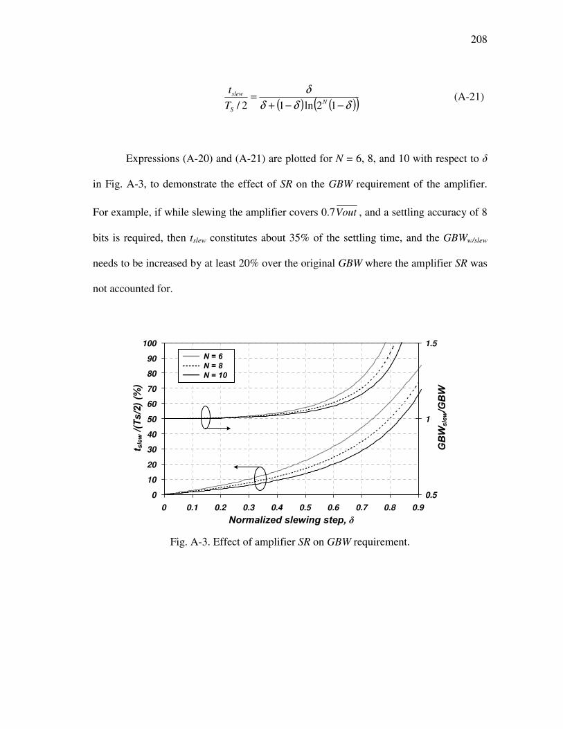
208
( ) ( )( )δδδ
δ
−−+=
12ln12/ N
S
slew
T
t (A-21)
Expressions (A-20) and (A-21) are plotted for N = 6, 8, and 10 with respect to δ
in Fig. A-3, to demonstrate the effect of SR on the GBW requirement of the amplifier.
For example, if while slewing the amplifier covers 0.7Vout , and a settling accuracy of 8
bits is required, then tslew constitutes about 35% of the settling time, and the GBWw/slew
needs to be increased by at least 20% over the original GBW where the amplifier SR was
not accounted for.
0
10
20
30
40
50
60
70
80
90
100
0 0.1 0.2 0.3 0.4 0.5 0.6 0.7 0.8 0.9
0.5
1
1.5
t sle
w/(
Ts
/2)
(%)
GB
Wsle
w/G
BW
Normalized slewing step, δ
N = 6
N = 8
N = 10
Fig. A-3. Effect of amplifier SR on GBW requirement.

209
APPENDIX B
MDAC NOISE ANALYSIS WITH ACTIVE SAMPLING
Switches and amplifiers are the fundamental contributors to the noise seen at the
output of an MDAC. All noise sources present for both the sampling and holding phases
in an M bit/stage MDAC are shown in Fig. B-1. Here, the power spectral density of the
amplifier’s input referred noise is denoted by 2
, Anv , whereas the subscripts fb, and 0
through m, where m = 2M
-1, represent the feedback and input switches and capacitors
respectively. The forthcoming analysis will aim to find the total noise at the output to see
how the switches and amplifier affect the MDAC noise performance.
(a) (b)
C0
A(s)
Cm
R0
Rm
Rfbv
2n,0
v2n,m
v2n,fb
*
v2n,out
v2n,A
C1
A(s)
Cm
R1
Rm
R0v
2n,1
v2n,m
v2n,0
*
v2
n,out
v2n,A
C0
x x
Fig. B-1. Noise sources present in an M bit/stage MDAC for (a) sampling phase and (b)
holding phase.
Beginning with the sampling phase, the integrated noise on each capacitor is
examined. Referring to Fig. B-1(a), and using R0 ..Rm=Rsw, and C0 ..Cm=Cu, the circuit
can be described by (B-1)-(B-3). Here, A(s) is the amplifier transfer function and is
defined by ωu/s for simplicity, where ωu is the amplifier unity gain frequency.

210
( )[ ] ( ) 01
1
0
,,, =
−
+++− ∑
=
m
i
inx
usw
u
fbnoutnx
sw
vvCsR
sCvvv
R (B-1)
( )( ) ( )xAnu
xAnoutn vvs
vvsAv −≅−= ,,,
ω (B-2)
( )usw
nx
CnCsR
vvv
+
−=
1
0,
, 0 (B-3)
By substituting (B-1) and (B-2) into (B-3), the noise power stored on C0 can be
expressed as shown in (B-4), where H1(s), H2(s), H3(s) and H4(s) are given by (B-5), (B-
6), (B-7) and (B-8) respectively.
( ) ( ) ( ) ( ) ∑=
⋅+⋅+⋅+⋅=m
i
infbnAnnCn vsHvsHvsHvsHv1
2
,
2
4
2
,
2
3
2
,
2
2
2
0,
2
1
2
, 0 (B-4)
( )( )
( ) ( )
++
+++
++
++
−=
21
11
11
1
2
2
1
mCR
sCRsCsR
mCR
sCRs
sH
u
uswusw
u
usw
u
uswusw
u
ωω
ωω (B-5)
( )( )2
11
1
2
2
++
++
=
mCR
sCRs
sH
u
uswusw
u ωω
(B-6)
( )( )2
11 2
3
++
++
=
mCR
sCRs
s
sH
u
uswusw
u
u
ωω
ω (B-7)

211
( )( ) ( )
++
+++
=
21
11 2
2
4
mCR
sCRsCsR
CRs
sH
u
uswusw
u
usw
u
usw
ωω
ω (B-8)
Next, the square magnitude of H1(s), H2(s), H3(s) and H4(s) is to be integrated
over the frequency range 0,∞ to find the total noise power. A closed form solution for
these integrals, however, is not easily achieved due to the complex roots of the second
order transfer function in the numerator of (B-5) and denominators of (B-5)-(B-8). To
alleviate this difficulty, we can drop the term (m+1) and (m+2) from (B-5)-(B-8) thereby
transforming (B-5)-(B-8) to (B-9)-(B-12) respectively.
( )( )uswCsR
sH+
−=1
11 (B-9)
( )( )
++
=
u
usw
sCsR
sH
ω11
12 (B-10)
( )( )
++
=
u
usw
u
sCsR
s
sH
ω
ω
11
3 (B-11)
( )( )
++
=
u
usw
u
usw
sCsR
CRs
sH
ω
ω
112
2
4 (B-12)

212
Naturally, the simplification introduces an error, which is clearly visible in Fig.
(B-2), where (B-5)-(B-8) are plotted for m = 1, 2, 3, along with (B-9)-(B-12); the values
for Rsw, Cu and ωu used in the plots were 100Ω, 1pF and 5G rad/s respectively.
Fig. B-2. The magnitude plots of the original and simplified transfer function; (a) H1(s),
(b) H2(s), (c) H3(s) and (d) H4(s).
While, this shows that (B-9)-(B-12) will yield an over estimate for the integrated
noise, the resulting closed form integrals make for a more useable hand calculations tool

213
that inherently leaves a comfortable margin for design error. The final integral values are
now given in (B-13)-(B-16).
( )uswCR
dfsH4
1
0
2
1 =⋅∫∞
(B-13)
( )
+
=⋅∫∞
uswu
uswCR
CR
dfsH
ω
114
1
0
2
2 (B-14)
( )( )uswuusw CRCR
dfsHω+
=⋅∫∞
14
1
0
2
3 (B-15)
( )
++
=⋅∫∞
uswu
uswuusw
CR
CRCR
dfsH
ω
ω
118
1222
0
2
4 (B-16)
The computed integrals of (B-13)-(B-16) can now be substituted in (B-4) to get
the total noise power sampled on C0, which is given by (B-17).
( )
++
+
++
+
+=
∑=
uswu
uswuusw
m
i
in
uswuusw
fbn
uswu
usw
An
usw
n
Cn
CR
CRCR
v
CRCR
v
CRCR
v
CR
vv
ω
ω
ω
ω
114
14114
4
222
1
,
2
,
2
,
2
0,2
, 0
(B-17)
The thermal noise power spectral density of a resistor is defined by (B-18) [44],

214
while the input referred noise of an amplifier can be modeled by (B-19) [49], where gm
is the input pair transconductance, γ is a process dependent excess noise co-efficient and
η is the amplifier architecture noise factor.
fTRkv swBswn ∆⋅= 42
, (B-18)
( )
fgm
Tkv B
An ∆ηγ
⋅+
=142
, (B-19)
Using (B-18) and (B-19) in (B-17) yields the final form of 2
, 0Cnv , which is the
same for any 2
, iCnv as the characteristic equations (B-1)-(B-3) apply to any capacitor in
Fig. B-1(a). The final result is given in (B-20). During the holding phase, Fig. B-1(b), all
the noise power stored on the capacitors C0 ..Cm is transferred to the now feedback
capacitor C0. Therefore the sampling phase component of the output noise can be
expressed by (B-21).
( )
+
++
++
++
+=
uswu
sw
uswu
uswuuswuu
BCn
CRgmR
CR
CR
m
CRC
Tkv
Si
ω
ηγ
ω
ωωΦ 11
1
112
1
11
222
2
, (B-20)
( )S
iS
i
S
SCn
m
Cn
totn
outn vmvC
Qv
ΦΦΦ
2
,
0
2
,2
0
2
,2
, 1 ⋅+=== ∑ (B-21)
As for the holding phase component of the output noise, it can be evaluated using

215
Fig. B-1(b), which is characterized by (B-22) and (B-23).
( ) ( ) 00
,,, =−++− ∑=
m
i
inxfbnoutnx vvvvv (B-22)
( )( ) ( )xAnu
xAnoutn vvs
vvsAv −≅−= ,,,
ω (B-23)
Using (B-22) and (B-23) to eliminate vx, the output noise power in the holding
phase, H
outnvΦ
2
, , can be expressed by (B-24), where H5(s) is given by (B-25).
( ) ( )
++⋅= ∑
=
m
i
inAnoutn vvmsHvH
1
2
,
2
,
2
5
2
, 1Φ
(B-24)
( )( )
u
mssH
ω
11
15 +
+
= (B-25)
For the final form of the holding phase output noise, the square magnitude of
H5(s) is integrated over the frequency range 0,∞, and (B-18) and (B-19) are substituted
for 2
,inv and 2
, Anv respectively. This results in (B-26), where ωu is substituted with gm/CL,
and CL being the effective loading capacitance.
( )( )[ ]112
, +++= mgmRC
Tkv sw
L
Boutn
H
ηγΦ
(B-26)

216
The total noise seen at the output of the MDAC is the summation of (B-21) and
(B-26), and is given in (B-27) where αn is described by (B-28). Note that (B-21) is
doubled for a fully differential implementation as well as the effect of the switch
resistance in (B-26). Also, it is common practice to refer this noise to the input of the
pipeline cell for a meaningful comparison with the input signal. This is accomplished by
simply normalizing the output noise to the square of the MDAC gain (m+1), and is
demonstrated by (B-29).
( )( )[ ] ( ) ( )n
u
Bsw
L
B
MDACoutn
C
TkmmgmR
C
Tkv αηγ ++++++= 1121122
, (B-27)
( )
+
++
++
++
=
uswu
sw
uswu
uswuuswu
n
CRgmR
CR
CR
m
CR
ω
ηγ
ω
ωωα
11
1
112
1
1222
(B-28)
( )
( )( ) ( )
( )n
u
Bsw
L
B
MDACinn
Cm
Tk
m
gmR
Cm
Tkv αηγ +
++
+++
+= 1
12
1
21
1
2
, (B-29)
In conclusion, the noise contributions of the switches and amplifier to the MDAC
noise are limited by the unit capacitance, Cu, used in the MDAC and the effective
loading capacitance, CL, seen by the amplifier. Moreover, the use of multi-bit/stage
pipeline cells has an added filtering effect on the total noise. However, this added benefit
of lower noise is a direct trade-off with the speed of the pipeline ADC.

217
APPENDIX C
OPERATIONAL TRANSCONDUCTANCE AMPLIFIER PARAMETERS
Referring to the OTAs in Fig. 46, the following is a summary of key performance
metrics expressions, based on the following assumptions: all amplifiers are driving a
capacitive load CL, cascode devices are treated as source degenerated devices for noise
and offset calculations and hence are neglected due to their small transconductance, and
finally M denotes the transistor aspect ratio W/L.
A. Telescopic OTA (TL)
1gmGmTL = (C-1)
( )7553131)0( dsdsdsdsOUTTL rrgmrrgmgmRGmA ⋅≅= (C-2)
−
−= −−
2
1
1
1 tantan180PP
GBWGBWPM
ωω (C-3)
3
321
1 ,1
,gs
P
LOUT
P
L C
gm
CRC
gmGBW ≅== ωω (C-4)
L
T
C
ISR = (C-5)
Ttotal
TL
I
gm
I
Gm 1==η (C-6)
fM
M
MIC
Tkf
gm
gm
gm
Tkv
P
N
DoxP
iT ∆µ
µ
µ
γ∆
γ⋅
+=⋅
+=
1
3
11
B
1
3
1
B2 12
81
8 (C-7)

218
fL
L
K
K
fCLW
Kf
L
K
L
K
fCgm
Iv
FP
FN
oxP
FPFNFP
ox
D
fi
∆µ
∆ ⋅
+=⋅
+=
2
7
1
2
11
2
7
2
1
2
1
2
1 12
(C-8)
FN
FP
fi K
KLLv 71
min
2
1 =⇒ (C-9)
( )
+=
2
7
1
2
11
2
2 12L
L
A
A
LW
AV
TP
TNTP
V
V
P
NV
OSµ
µσ (C-10)
( )TN
TP
V
V
N
POS
A
ALLV ⋅=⇒
µ
µσ 31
min
2 (C-11)
B. Current Mirror OTA (CM)
1gmKGmCM ⋅= (C-12)
( )11995771)0( dsdsdsdsOUTCM rrgmrrgmgmKRGmA ⋅⋅≅= (C-13)
−
−
−= −−−
3
1
2
1
1
1 tantantan180PPP
GBWGBWGBWPM
ωωω (C-14)
( )KC
gm
C
gm
CRC
gmKGBW
gs
P
gs
P
LOUT
P
L +≅≅=
⋅=
1,,
1,
3
32
7
721
1 ωωω (C-15)
L
T
C
IKSR
⋅= (C-16)
( )
Ttotal
CM
IK
gmK
I
Gm
1
1
+
⋅==η (C-17)
fM
M
KM
M
KM
M
MIC
Tk
fgmK
gm
gmK
gm
gm
gm
gm
Tkv
P
N
P
N
DoxP
iT
∆µ
µ
µ
µ
µ
γ
∆γ
⋅
++
+=
⋅
+++=
1
11
2
1
5
2
1
3
11
B
1
2
11
1
2
5
1
3
1
B2
111
2
8
18
(C-18)

219
fL
L
KL
L
K
K
KL
L
K
K
fCLW
K
fL
KK
L
KK
L
KK
L
KK
fCgm
Iv
FP
FN
FP
FN
oxP
FP
FPFNFNFP
ox
D
fi
∆µ
∆
⋅
+
+
+=
⋅
+++=
2
11
1
2
5
1
2
3
1
2
11
2
11
2
5
2
3
2
2
1
2
2
1
2
1
111
2
(C-19)
212
11
2
5
2
3
1
min
2
1
11111−
+
+
=⇒
LKLK
K
KLK
KLv
FP
FN
FP
FN
fi
(C-20)
( )
+
+
+=
2
11
1
2
5
1
22
3
1
2
11
2
2 1112
L
L
KL
L
A
A
KL
L
A
A
LW
AV
TP
TN
TP
TNTP
V
V
P
N
V
V
P
NV
OSµ
µ
µ
µσ (C-21)
( )
212
11
2
5
22
3
2
1min
2 11111
−
+
+
=⇒
LKLA
A
KLA
ALV
TP
TN
TP
TN
V
V
P
N
V
V
P
NOS
µ
µ
µ
µσ (C-22)
C. Folded Cascode OTA (FC)
1gmGmFC = (C-23)
( )( )97731551)0( dsdsdsdsdsOUTFC rrgmrrrgmgmRGmA ⋅≅= (C-24)
−
−= −−
2
1
1
1 tantan180PP
GBWGBWPM
ωω (C-25)
5
521
1 ,1
,gs
P
LOUT
P
L C
gm
CRC
gmKGBW ≅=
⋅= ωω (C-26)
L
T
C
ISR = (C-27)
Ttotal
FC
I
gm
I
Gm
2
1==η (C-28)

220
fM
M
M
M
MIC
Tkf
gm
gm
gm
gm
gm
Tkv
P
N
DoxP
iT ∆µ
µ
µ
γ∆
γ⋅
+
+=⋅
++=
1
9
1
3
11
B
1
9
1
3
1
B2 212
81
8 (C-29)
fL
L
L
L
K
K
fCLW
K
fL
K
L
K
L
K
fCgm
Iv
FP
FN
oxP
FP
FNFNFP
ox
D
fi
∆µ
∆
⋅
+
+=
⋅
++=
2
9
1
2
3
1
2
11
2
9
2
3
2
1
2
1
2
1
21
22
(C-30)
212
9
2
3
1
min
2
1
112
−
+
=⇒
LLK
KLv
FP
FN
fi
(C-31)
( )
+
+=
2
9
1
2
3
1
2
11
2
2 212L
L
L
L
A
A
LW
AV
TP
TNTP
V
V
P
NV
OSµ
µσ (C-32)
( )
212
9
2
3
2
1min
2 112
−
+
=⇒
LLA
ALV
TP
TN
V
V
P
NOS
µ
µσ (C-33)

221
VITA
Rida Shawky Assaad received his Bachelor of Science degree in electrical
engineering from Texas A&M University in May 2002. He joined the Analog and Mixed
Signal Center at Texas A&M University in August 2002 and received his Ph.D. degree
in electrical engineering in December 2009. During 2005 he was an assistant lecturer at
the Electrical and Computer Engineering Department where he taught the introductory
course to electronics. He was an intern IC designer with Mobile Integrated Solutions at
Texas Instruments, Dallas, in the fall of 2007 and 2008. His research interests include
the design and optimization of base-band amplifiers and high resolution analog-to-digital
converters.
Mr. Assaad can be reached at the Analog and Mixed Signal Center, Weisenbaker
Engineering Research Center, Texas A&M University, College Station, TX 77843-3128.
His email address is: [email protected].