Embed Size (px)
Citation preview
Design-Analysis (Thermal and Mechanical) Integration Research for Electronic Packaging
1Ryuichi Matsuki, 3Russell S. Peak, 2Sai Zeng, 3Miyako W. Wilson, 2Injoong Kim, 2Manas Bajaj
1Advanced Product Design & Development Div.
Shinko Electric Industries Co., Ltd. 2Engineering Information System Lab, 3Manufacturing Research Center,
Georgia Institute of Technology Abstract:
Simulating the characteristics of electronic packages like thermal resistance, thermomechanical stress distribution and electromagnetics is important to guide and verify their design. Since packages consist of densely packed components of varied materials and shapes, the simulation time for generating their finite element analysis (FEA) models can span from hours to days.
This paper overviews efforts to develop an automated tool aimed at one phase for CAD-CAE integration, that is FEA modeling. Automating idealized body decomposition and the use of SOAP have enabled a large -scale time reduction in FEA of packages while simultaneously providing the freedom to perform simulations across multiple platforms over the Internet. Additionally, proof-of-concept usage of STEP-based information models for chip packages (ISO 10303-210) holds promise for overcoming additional barriers in heteroge neous CAD-CAE transformations. Nomenclature ABB analysis building block API application programming interface APM analyzable product model EBGA enhanced ball grid array CBAM context-based analysis model COB constrained object FEA finite element analysis MRA multi-representation architecture SOAP Simple Object Access Protocol SMM solution method model STEP Standard for Exchange of Product Model Data (ISO 10303) XCP XaiTools ChipPackage™
Introduction: There is a pressing need to reduce the time and
cost of product realization in the area of electronics packaging. Use of CAE tools to simulate package behavior is growing at an accelerating pace to reduce the need for physical measurements and trial production iterations. However, current tools do not fully address the needs of Concurrent Engineering especially for CAD-CAE integration in the thermal and mechanical areas.
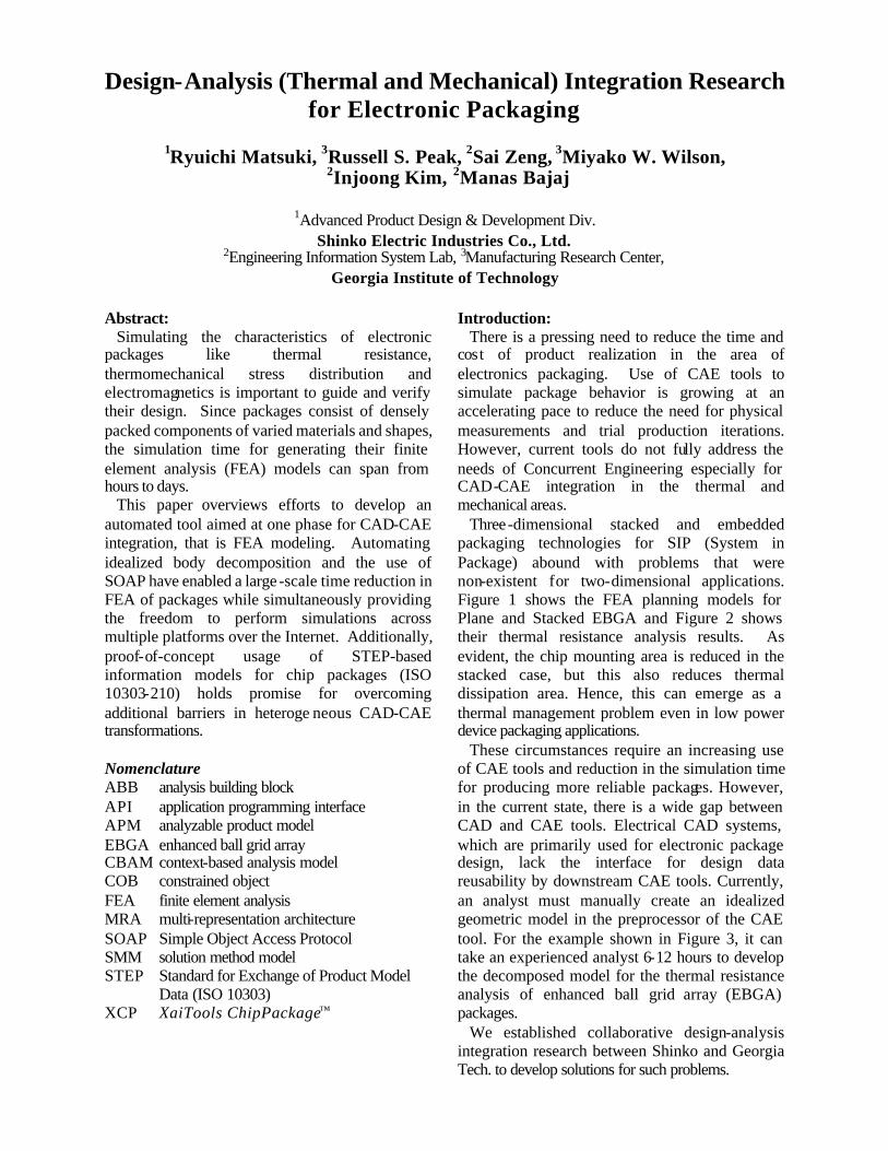
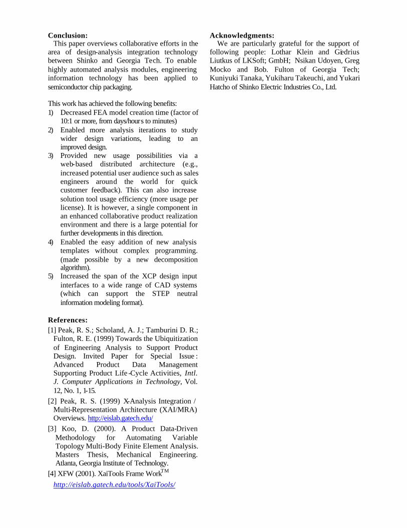
Three-dimensional stacked and embedded packaging technologies for SIP (System in Package) abound with problems that were non-existent for two-dimensional applications. Figure 1 shows the FEA planning models for Plane and Stacked EBGA and Figure 2 shows their thermal resistance analysis results. As evident, the chip mounting area is reduced in the stacked case, but this also reduces thermal dissipation area. Hence, this can emerge as a thermal management problem even in low power device packaging applications.
These circumstances require an increasing use of CAE tools and reduction in the simulation time for producing more reliable packages. However, in the current state, there is a wide gap between CAD and CAE tools. Electrical CAD systems, which are primarily used for electronic package design, lack the interface for design data reusability by downstream CAE tools. Currently, an analyst must manually create an idealized geometric model in the preprocessor of the CAE tool. For the example shown in Figure 3, it can take an experienced analyst 6-12 hours to develop the decomposed model for the thermal resistance analysis of enhanced ball grid array (EBGA) packages.
We established collaborative design-analysis integration research between Shinko and Georgia Tech. to develop solutions for such problems.
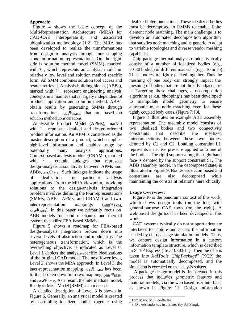
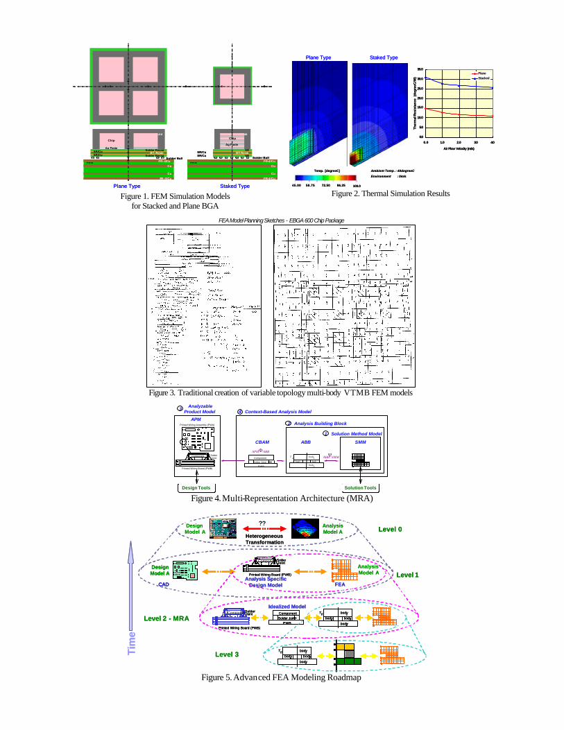
Approach: Figure 4 shows the basic concept of the
Multi-Representation Architecture (MRA) for CAD-CAE interoperability and associated ubiquitization methodology [1,2]. The MRA has been developed to realize the transformations from design to analysis through four stepping stone information representations. On the right side is solution method model (SMM), marked with ? , which represents an analysis model in relatively low level and solution method specific form. An SMM combines solution tool access and results retrieval. Analysis building blocks (ABBs), marked with ? , represent engineering analysis concepts in a manner that is largely independent of product application and solution method. ABBs obtain results by generating SMMs through transformations, ABBΨSMM, that are based on solution method considerations.
Analyzable Product Model (APMs), marked with ? , represent detailed and design-oriented product information. An APM is considered as the master description of a product, which supplies high-level information and enables usage by potentially many analysis applications. Context-based analysis models (CBAMs), marked with ? , contain linkages that represent design-analysis associativity between APMs and ABBs, APMΦABB. Such linkages indicate the usage of idealizations for particular analysis applications. From the MRA viewpoint, providing solutions to the design-analysis integration problem involves defining the four representations (SMMs, ABBs, APMs, and CBAMs) and two inter-representation mappings (ABBΨSMM,
APMΦABB). In this paper we primarily focus on ABB models for solid mechanics and thermal systems that utilize FEA-based SMMs.
Figure 5 shows a roadmap for FEA-based design-analysis integration broken down into several levels of abstraction and modularity. The heterogeneous transformation, which is the overarching objective, is indicated as Level 0. Level 1 depicts the analysis-specific idealizations of the original CAD model. The next lower level, Level 2, shows the MRA approach. In Level 3, the inter-representation mapping ABBΨSMM has been further broken down into two mappings ABBΨRMM and RMMΨSMM. As a result, the intermediate model, Ready-to-Mesh Model (RMM) is introduced.
A detailed description of Level 3 is shown in Figure 6. Generally, an analytical model is created by assembling idealized bodies together using
idealized interconnections. These idealized bodies must be decomposed to RMMs to enable finite element node matching. The main challenge is to develop an automated decomposition algorithm that satisfies node matching and is generic to adapt to variable topologies and diverse vendor meshing capabilities.
Chip package thermal analysis models typically consist of a number of idealized bodies (e.g., 20-30 bodies) of different materials (e.g., 10 or so). These bodies are tightly packed together. Thus the meshing of one body can strongly impact the meshing of bodies that are not directly adjacent to it. Targeting those challenges, a decomposition algorithm (a.k.a. chopping1) has been developed2 to manipulate model geometry to ensure automatic mesh node matching even for these tightly coupled body cases. (Figure 7) [3].
Figure 8 illustrates an example ABB assembly representation. The assembly model consists of two idealized bodies and two connectivity constraints that describe the idealized interconnections between these two bodies, denoted by C1 and C2. Loading constraint L1 represents an active pressure applied onto one of the bodies. The rigid support along the right hand face is denoted by the support constraint S1. The ABB assembly model, in the decomposed state, is illustrated in Figure 9. Bodies are decomposed and constraints are also decomposed while maintaining the constraint relations hierarchically. Usage Overview:
Figure 10 is the panorama context of this work, which shows design tools (on the left) with general-purpose CAE tools (on the right). A web-based design tool has been developed in this work.
CAD systems typically do not support adequate interfaces to capture and access the information needed by chip package simulation models. Thus, we capture design information in a custom information template structure, which is described in STEP Express (ISO 10303-11). Then the data is taken into XaiTools ChipPackage™ (XCP) the model is automatically decomposed, and the simulation is executed on the analysis solvers.
A package design model is first created in this process that includes geometric features and material models, via the web-based user interface, as shown in Figure 11. Design information
1 Tom Mack, MSC Software. 2 PhD thesis underway in this area (by Sai Zeng).
transformed to the custom STEP-based description is then taken into XCP. XCP is developed as an end-user-oriented STEP-Book application (a technology initiated by LKSoft, GmbH). Figure 12 shows an example of the EBGA thermal analysis model view. The model information tree, displayed on the left side and the information regarding the specific leaves, as shown on the right side, enables the user to easily retrieve the needed information (e.g. chip size, young’s modules, etc.).
XCP also provides three-dimensional geometric model viewer capabilities based on standard STEP capabilities (ISO 10303-514). Undecomposed and decomposed ABB assembly views are shown in Figure13, 14. Operations such as pan, zoom and rotate can be perfor med in the 3D viewer, for a detailed view of the geometric model, using simple mouse operations.
The step-by-step operation procedure for thermal analysis in XCP is performed in the order shown in Figure 15 (or a single button push is possible to run everything all at once). “Solve ABB” solves for the geometrical relations of ABB. Then, “Chop ABB” decomposes the ABB. An SMM for a preprocessor (PATRAN)-dependent model, is created in the next step: “Setup FEA SMM”. “Solve FEA” executes the analysis solver (ABAQUS) on the said SMM.
After the analysis job has been done, “Update FEA SMM” loads the results back into XCP and transforms them from generic FEA data into chip package-specific knowledge (e.g., thermal resistance values). XCP displays the computed numerical and graphical results. Figure 16 is an example for EBGA thermal resistance results that displays temperature values and distribution contour. In the stress analysis case, deformation, stress distribution contours, and maximum and minimum stresses on each block are displayed.
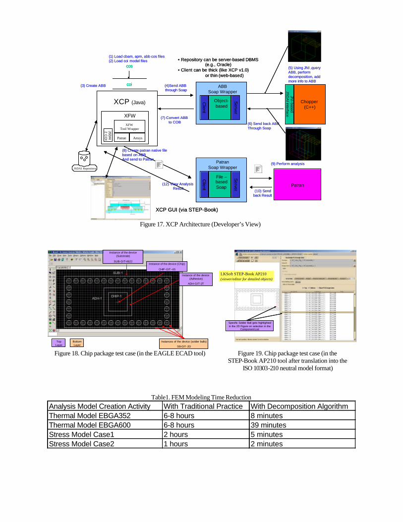
XCP uses an Internet standard called SOAP3 (Simple object access Protocol), which enables the access to the solver server from a remote client across the Web. Data exchange and remote procedure calls are done between the client and server. Thereby, an efficient system operation is achieved by distributing low memory intensive operations like XCP usage on the client side and high memory intensive tasks like decomposition
3 SOAP is an Internet protocol based on XML, which performs a remote procedure call and data exchange in order to achieve automated web services. See www.w3.org for further information.
module execution and FEA solution on the server side (Figure 17). These operations have successfully been tested between Shinko (Nagano, Japan) and Georgia Tech (Atlanta, GA, USA).
Ideally standards -based CAD models could be leveraged directly from the CAD tools. A trial data translation example from CAD to STEP -Book AP210 is shown in Figure 18. This test design is an assembly model that consists of a simplified chip, the substrate and solder balls. This test design was captured in the EAGLE 4 electrical CAD system (CadSoft Computer GmbH) since a STEP AP210 translator was already available for it (by LKSoftWare , GmbH). The translated information model for this example is shown in Figure 19. The detailed information about the selected solder ball instance (left side figure) is displayed in the table (on the right side).
STEP AP210 interfaces for other ECAD tools like Zuken and Mentor Graphics are now at the alpha level of development at LKSoft5. Hence, in the future, tools like XCP will be able to more easily support analysis simulations for electronic packages designed across varied CAD systems that have an AP210 interface or a converter.
Results:
Based on industrial usage and testing, Table 1 summarizes the analyst efforts required for model creation activities for various analysis models. In the case of thermal analysis, it takes 6-8 hours to create the thermal analysis model using the traditional method. On the other hand with the use of the new concurrent engineering tool, XCP, the modeling time has reduced from 8 hours to 39 minutes. Reduction in the modeling time is of the same order even in the case of stress analysis. Although the decomposition time increases for complex models, the manual effort is still greatly reduced, and we expect further improvements in decomposition algorithm efficiency.
XCP combined with this new decomposition algorithm has the capability to add analysis templates for new types of packages without complex programming. Furthermore, this tool has paved the way for simulation usage by people who do not have detailed knowledge about analysis simulations (e.g. design and sales engineers) by the application of interoperability and Internet technologies.
4 See http://www.cadsoft.de for more information. 5 See www.lksoft.com for examples and the latest status.
Conclusion: This paper overviews collaborative efforts in the
area of design-analysis integration technology between Shinko and Georgia Tech. To enable highly automated analysis modules, engineering information technology has been applied to semiconductor chip packaging. This work has achieved the following benefits: 1) Decreased FEA model creation time (factor of
10:1 or more, from days/hours to minutes) 2) Enabled more analysis iterations to study
wider design variations, leading to an improved design.
3) Provided new usage possibilities via a web-based distributed architecture (e.g., increased potential user audience such as sales engineers around the world for quick customer feedback). This can also increase solution tool usage efficiency (more usage per license). It is however, a single component in an enhanced collaborative product realization environment and there is a large potential for further developments in this direction.
4) Enabled the easy addition of new analysis templates without complex programming. (made possible by a new decomposition algorithm).
5) Increased the span of the XCP design input interfaces to a wide range of CAD systems (which can support the STEP neutral information modeling format).
References: [1] Peak, R. S.; Scholand, A. J.; Tamburini D. R.;
Fulton, R. E. (1999) Towards the Ubiquitization of Engineering Analysis to Support Product Design. Invited Paper for Special Issue : Advanced Product Data Management Supporting Product Life -Cycle Activities, Intl. J. Computer Applications in Technology, Vol. 12, No. 1, 1-15.
[2] Peak, R. S. (1999) X-Analysis Integration / Multi-Representation Architecture (XAI/MRA) Overviews. http://eislab.gatech.edu/
[3] Koo, D. (2000). A Product Data-Driven Methodology for Automating Variable Topology Multi-Body Finite Element Analysis. Masters Thesis, Mechanical Engineering. Atlanta, Georgia Institute of Technology.
[4] XFW (2001). XaiTools Frame WorkTM http://eislab.gatech.edu/tools/XaiTools/
Acknowledgments: We are particularly grateful for the support of
following people: Lothar Klein and Giedrius Liutkus of LKSoft; GmbH; Nsikan Udoyen, Greg Mocko and Bob. Fulton of Georgia Tech; Kuniyuki Tanaka, Yukiharu Takeuchi, and Yukari Hatcho of Shinko Electric Industries Co., Ltd.
Mold
Chip
Ag Paste
FR-4Cu
Cu
Solder BallFR-4/Cu
FR-4/Cu
Plane Type Staked Type
BT-Resin Solder Resist
Solder Resist
Mold
FR-4Cu
Cu
Solder BallFR-4/Cu
FR-4/Cu
Chip
Ag Paste
BT-ResinSR
SRSR/Cu SR/Cu
SR/Cu SR/Cu
Mold
Chip
Ag Paste
FR-4Cu
Cu
Solder BallFR-4/Cu
FR-4/Cu
Plane Type Staked Type
BT-Resin Solder Resist
Solder Resist
Mold
FR-4Cu
Cu
Solder BallFR-4/Cu
FR-4/Cu
Chip
Ag Paste
BT-ResinSR
SRBT-Resin
SR
SRSR/Cu SR/Cu
SR/Cu SR/Cu
Figure 1. FEM Simulation Models
for Stacked and Plane BGA
Temp. [degreeC]
45.00 58.75 72.50 86.25 100.0
Plane Type Staked Type
Ambient Temp. : 40degreeC
Environment : 0m/s
0.0
5.0
10.0
15.0
20.0
25.0
30.0
35.0
0.0 1.0 2.0 3.0 4.0
Air Flow Velocity (m/s)
Ther
mal
Res
ista
nce
(de
gree
C/W
)
PlaneStacked
Temp. [degreeC]
45.00 58.75 72.50 86.25 100.0
Plane Type Staked Type
Ambient Temp. : 40degreeC
Environment : 0m/s
0.0
5.0
10.0
15.0
20.0
25.0
30.0
35.0
0.0 1.0 2.0 3.0 4.0
Air Flow Velocity (m/s)
Ther
mal
Res
ista
nce
(de
gree
C/W
)
PlaneStacked
Figure 2. Thermal Simulation Results
FEA Model Planning Sketches - EBGA 600 Chip Package
Figure 3. Traditional creation of variable topology multi-body VTMB FEM models
1 Solution Method Model
ΨABB SMM
2 Analysis Building Block
4 Context-Based Analysis Model3
SMMABB
ΦAPM ABB
CBAM
APM
Design Tools Solution Tools
Printed Wiring Assembly (PWA)
Solder Joint
Component
PWB
body 3body
2
body1
body4
T0
Printed Wiring Board (PWB)
SolderJoint
Component
AnalyzableProduct Model
Figure 4. Multi-Representation Architecture (MRA)
CAD
DesignModel A
FEA
AnalysisModel A
Heterogeneous Transformation
??Level 0
DesignModel A
AnalysisModel A
Printed Wiring Board (PWB)
SolderJoint
Component
Analysis Specific Design Model
Level 1
Solder JointComponent
PWB
body3body2
body1body4
T0
Printed Wiring Board (PWB)
SolderJointComponent
Level 2 - MRA body3body2
body1body4
T0
Level 3Tim
e
Idealized Model
CAD
DesignModel A
CAD
DesignModel A
FEA
AnalysisModel A
Heterogeneous Transformation
??Level 0
DesignModel A
AnalysisModel A
Printed Wiring Board (PWB)
SolderJoint
Component
Printed Wiring Board (PWB)
SolderJoint
Component
Analysis Specific Design Model
Level 1
Solder JointComponent
PWBSolder JointComponent
PWB
body3body2
body1body4
T0body3
body2
body1body4
T0
Printed Wiring Board (PWB)
SolderJointComponent
Printed Wiring Board (PWB)
SolderJointComponent
Level 2 - MRA body3body2
body1body4
T0body3
body2
body1body4
T0
Level 3Tim
e
Idealized Model
Figure 5. Advanced FEA Modeling Roadmap
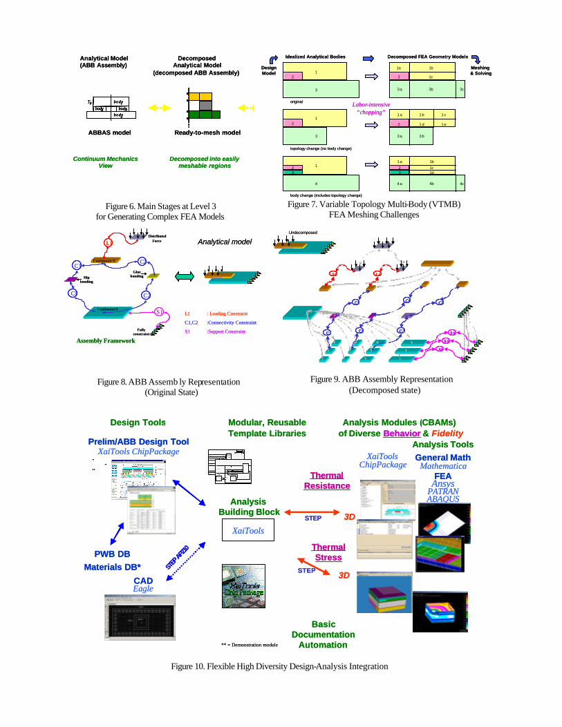
Analytical Model(ABB Assembly)
DecomposedAnalytical Model
(decomposed ABB Assembly)
Continuum MechanicsView
Decomposed into easilymeshable regions
body3body2
body1body4
T0body3
body2
body1body4
T0
ABBAS model Ready-to-mesh model
Analytical Model(ABB Assembly)
DecomposedAnalytical Model
(decomposed ABB Assembly)
Continuum MechanicsView
Decomposed into easilymeshable regions
body3body2
body1body4
T0body3
body2
body1body4
T0
ABBAS model Ready-to-mesh model
Figure 6. Main Stages at Level 3 for Generating Complex FEA Models
12
3
12
3
12
4
1a
2
3a
1b
1c
3b 3c
3a 3b
2
1a 1b 1c
1d 1e
3
1a 1b
1c1d
23
4a 4b 4c
Idealized Analytical Bodies Decomposed FEA Geometry Models
original
topology change (no body change)
body change (includes topology change)
Labor-intensive “chopping”
Meshing & Solving
DesignModel 1
2
3
12
3
12
4
1a
2
3a
1b
1c
3b 3c
3a 3b
2
1a 1b 1c
1d 1e
3
1a 1b
1c1d
23
4a 4b 4c
Idealized Analytical Bodies Decomposed FEA Geometry Models
original
topology change (no body change)
body change (includes topology change)
Labor-intensive “chopping”
Meshing & Solving
DesignModel
Figure 7. Variable Topology Multi-Body (VTMB) FEA Meshing Challenges
Figure 8. ABB Assemb ly Representation (Original State)
Figure 9. ABB Assembly Representation
(Decomposed state)
Analysis Modules (CBAMs) of Diverse Behavior & Fidelity
FEAAnsys
PATRANABAQUS
General MathMathematica
XaiTools
XaiToolsChipPackage
ThermalResistance
3D
Modular, ReusableTemplate Libraries
temperature change, ∆T
material model
temperature, T
reference temperature, T o
cte, αyoungs modulus, E
force, F area, A stress, σ
undeformed length, L o
strain, ε
total elongation, ∆L
length, Lstart, x1end, x
2
mv6
mv5
smv1
m v 1mv4
E
α
One D LinearElastic Model
(no shear)
∆T
εσ
ε e
εt
thermal strain, ε t
elastic strain, εe
m v 3
m v 2
x
FF
E, A, α
∆ LLo
∆T , ε , σ
yL
r1
12 xxL −=r2
oLLL −=∆
r4
AF
=σ
sr1
oTTT −=∆
r 3
LL∆
=ε
material
effective length, L eff
deformation model
linear elastic model
L o
T o r s i o n a l Rod
G
ϕ
τ
J
γ
r
θ2
θ 1
shear modulus, G
cross section:ef fect ive r ing polar moment of inertia, J
al1
al3
al2a
l i n k a g e
mode: shaft torsion
condition reac t ionT
outer radius, ro al2b
stress mos model
allowable stress
twist mos m o d e l
Margin of Safety(> case)
al lowablea c t u a l
M S
Margin of Safety(> case)
al lowablea c t u a l
M S
allowablet w i s t
Analysis Tools
Design Tools
PWB DBMaterials DB*
Prelim/ABB Design ToolXaiTools ChipPackage
ThermalStress
3D
** = Demonstration module
BasicDocumentation
Automation
Analysis Building Block
CADEagle
STEP
AP210
STEP
STEP
Figure 10. Flexible High Diversity Design-Analysis Integration
L1 L1
C1 C1
C1 C1
C2
C 2 S 1
S 1
S1
Undecomposed
L1 L1
C1 C1
C1 C1
C2
C 2 S 1
S 1
S1
L1L1 L1L1
C1C1 C1C1
C1C1 C1C1
C2C2
C 2C 2 S 1S 1
S 1S 1
S1S1
Undecomposed
L1
C1C2
C1 C2
S1
Distributed Force
Slip bonding
Glue bonding
Continuum A
Continuum B
Fully constraint
Assembly Framework
L1 : Loading Constraint
C1,C2 :Connectivity Constraint
S1 :Support Constraint
Analytical modelL1L1
C1C2
C1 C2
S1
Distributed Force
Slip bonding
Glue bonding
Continuum A
Continuum B
Fully constraint
Assembly Framework
L1 : Loading Constraint
C1,C2 :Connectivity Constraint
S1 :Support Constraint
Analytical model
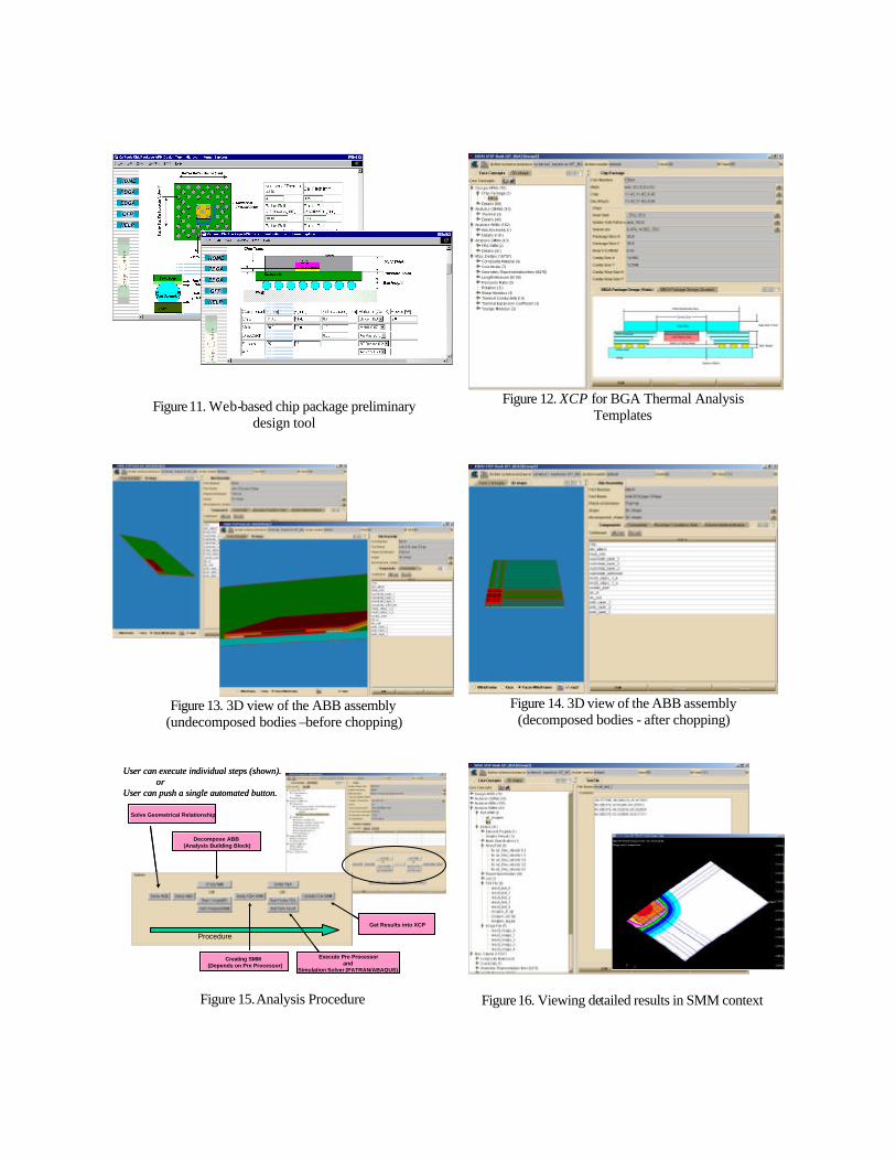
Figure 11. Web-based chip package preliminary design tool
Figure 12. XCP for BGA Thermal Analysis Templates
Figure 13. 3D view of the ABB assembly
(undecomposed bodies –before chopping)
Figure 14. 3D view of the ABB assembly
(decomposed bodies - after chopping)
Solve Geometrical Relationship
Procedure
Decompose ABB (Analysis Building Block)
Creating SMM (Depends on Pre Processor)
Execute Pre Processorand
Simulation Solver (PATRAN/ABAQUS)
Get Results into XCP
User can execute individual steps (shown). or
User can push a single automated button.
Solve Geometrical Relationship
Procedure
Decompose ABB (Analysis Building Block)
Creating SMM (Depends on Pre Processor)
Execute Pre Processorand
Simulation Solver (PATRAN/ABAQUS)
Get Results into XCP
User can execute individual steps (shown). or
User can push a single automated button.
Figure 15. Analysis Procedure
Figure 16. Viewing detailed results in SMM context
coi
cos
(1) Load cbam, apm, abb cos files(2) Load coi model files
JSDAI Repository
Chopper (C++)
(4)Send ABB through Soap
XCP (Java)
(5) Using JNI ,query ABB, perform decomposition, add more info to ABB
XFW Tool Wrapper
Patran Ansys
XFW
JSD
AI
2 CO
I
Patran
(8) Create patran native file based on ABBAnd send to Patran
Server
Client
File –based Soap
PatranSoap Wrapper
(9) Perform analysis
(12) View AnalysisResult
(10) Send back Result
(3) Create ABB
(6) Send back ABBThrough Soap
JNI-based
JSD
AI interface
Server
Client
Object-based
ABBSoap Wrapper
(7) Convert ABBto COB
• Repository can be server-based DBMS (e.g., Oracle)
• Client can be thick (like XCP v1.0) or thin (web-based)
XCP GUI (via STEP-Book)
coi
cos
coi
cos
(1) Load cbam, apm, abb cos files(2) Load coi model files
JSDAI RepositoryJSDAI Repository
Chopper (C++)
(4)Send ABB through Soap
XCP (Java)
(5) Using JNI ,query ABB, perform decomposition, add more info to ABB
XFW Tool Wrapper
Patran Ansys
XFW Tool Wrapper
Patran Ansys
XFW
JSD
AI
2 CO
I
Patran
(8) Create patran native file based on ABBAnd send to Patran
Server
Client
File –based Soap
Server
Client
File –based Soap
PatranSoap Wrapper
(9) Perform analysis
(12) View AnalysisResult
(10) Send back Result
(3) Create ABB
(6) Send back ABBThrough Soap
JNI-based
JSD
AI interface
Server
Client
Object-based
ABBSoap Wrapper
Server
Client
Object-based
Server
Client
Object-based
ABBSoap Wrapper
(7) Convert ABBto COB
• Repository can be server-based DBMS (e.g., Oracle)
• Client can be thick (like XCP v1.0) or thin (web-based)
XCP GUI (via STEP-Book)
Figure 17. XCP Architecture (Developer’s View)
Instance of the device (Chip)
CHIP-GIT -4S
Instance of the device (Adhesive)
ADH-GIT-2T
Instance of the device (Substrate)
SUB-GIT-4622
Instances of the device (solder balls)
SB-GIT -2D
Top Layer
Bottom Layer
Instance of the device (Chip)
CHIP-GIT -4S
Instance of the device (Adhesive)
ADH-GIT-2T
Instance of the device (Substrate)
SUB-GIT-4622
Instances of the device (solder balls)
SB-GIT -2D
Top Layer
Bottom Layer
Figure 18. Chip package test case (in the EAGLE ECAD tool)
Specific Solder Ball gets highlighted in the 2D Figure on selection in the
Component List
LKSoft STEP-Book AP210(viewer/editor for detailed objects)
Specific Solder Ball gets highlighted in the 2D Figure on selection in the
Component List
LKSoft STEP-Book AP210(viewer/editor for detailed objects)
Figure 19. Chip package test case (in the STEP-Book AP210 tool after translation into the
ISO 10303-210 neutral model format)
Table1. FEM Modeling Time Reduction
Analysis Model Creation Activity With Traditional Practice With Decomposition AlgorithmThermal Model EBGA352 6-8 hours 8 minutesThermal Model EBGA600 6-8 hours 39 minutesStress Model Case1 2 hours 5 minutesStress Model Case2 1 hours 2 minutes