Embed Size (px)
Citation preview
DEFENSEUS military researches GaNtransistors for X-band radar
Cree and Nichia signwhite-LED contract
InP lasers made on 4 inch HBT line
Kopin sets up InGaNjoint venture in Asia
ALSO INSIDE
March 2005 Volume 11 Number 2
MARCH 2005 VOLUME 11 NUMBER 2
Cree and Nichia agree a cross-license dealfor white-lighting technology. p5
Chips or rice? Agilent Technologies plots itsfuture path in consumer electronics. p28
A famous UK laboratory gets a new lease oflife as the Centre for Integrated Photonics. p16
5 Headline News Shareholders on warpath as improperaccounting plagues Veeco TurboDisc...Cree and Nichia combine forces on white lighting
8 GaAs & Wireless News Slowing phone market to top 700 m units in 2005...Filtronic is upbeat on prospects as it signs PHEMT supply deal...Endwave bags defense deal
11 Opto News DVD demand accelerates AlGaInP-market growth...Nichia develops UV and blue–green lasers...Laser-diode makers push power envelope
12 LED News Kopin sets up InGaN LED-production venture in Asia...III-N Technology unveils novel single-chip power AC-LED lamp
14 Fiber News 4 inch HBT wafer line makes InP lasers...BinOptics to scale up production following $10 m funding scoop
30 M&E News Kopin wins two patents covering GaAsInN HBT wafer technology...IQE order book grows
COMPOUND SEMICONDUCTOR MARCH 2005 1
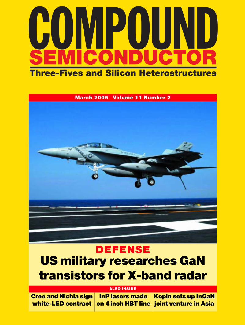
On the cover: GaN transistors could be an essential building block for the communication systems installed in next-generation unmanned air-combat systems(image courtesy of the US Navy).
NEWS
19 X-band radar is set to reap benefits of GaN technologyComplex US military projects demand an investment inhigh-technology equipment. Yvonne Carts-Powell tells ofsome progress that has been made with GaN transistors.
COVER STORY: DEFENSE
16 UK research center aims to exploit famed historyThe Centre for Integrated Photonics has inherited theintellectual property and wafer-processing equipment ofthe BT Photonics Technology Research Centre. RichardStevenson finds out what the start-up plans to do with it all.
23 Additional pipework opens up transistor applications for SiCPeter Wellmann describes a new approach to SiC substrategrowth that could improve LED and Schottky-diodeperformance, as well as pave the way for new devices.
27 Nichia marches on, Nakamura licks wounds and pays lawyersMichael Hatcher looks back at the blue-LED legal battlebetween Nichia and Shuji Nakamura and assesses thereaction of the two protagonists.
28 Agilent sets out its consumer vision for future profitabilityAgilent’s semiconductor product group is looking toincrease revenue from consumer electronics applications.Michael Hatcher reports on how they plan to achieve this.
FEATURES
Compound Semiconductor’s circulationfigures are audited by BPA International
32 Portfolio Slowdown of phone market is a challenge for GaAs industry
DEPARTMENTS
26 Suppliers Guide31 Product Showcase
ADVERTISING SECTION
CR
EE
AG
ILE
NT
CIP
Editor Michael [email protected]: +44 117 930 1013. Fax: +44 117 925 1942
Features editor Richard [email protected]: +44 117 930 1192
Consulting editor Tim [email protected]: +44 117 930 1233
Commercial manager Rebecca [email protected]: +44 117 930 1032. Fax: +44 117 930 1178
Sales executive Luke [email protected]: +44 117 930 1033. Fax: +44 117 930 1178
Circulation manager Jackie [email protected]: +44 117 930 1218. Fax +44 117 930 1178
Publisher Sarah [email protected]: +44 117 930 1020
Production Teresa RyanAd production Jackie Cooke, Tanwen HafArt directorAndrew GiaquintoTechnical illustratorAlison ToveyPublishing director Richard Roe
SubscriptionsAvailable free of charge to qualifying individualsworking at compound semiconductor fabs andfoundries. For further information visitcompoundsemiconductor.net/subscribe.Subscriptions for individuals not meeting qualifyingcriteria: individual £82/$148 US/7119; library£184/$331 US/7267. Orders to CompoundSemiconductor, WDIS, Units 12 & 13, CranleighGardens Industrial Estate, Southall, MiddlesexUB1 2DB, UK. Tel: +44 208 606 7518; Fax: +44 208 606 7303. General enquiries:[email protected].
7979 total qualified circulation*
*June 2004 BPA audit statement
Editorial boardMayank Bulsara (USA); Andrew CarterBookham Technology (UK); Jacob TarnEpistar/Gigacomm (Taiwan); Ian FergusonGeorgia Institute of Technology (USA); Toby StriteJDS Uniphase (Poland); Mark Wilson Motorola(USA); Dwight Streit Northrop Grumman (USA);Joseph Smart RF Micro Devices (USA);Colombo Bolognesi Simon Fraser University(Canada); Shuji Nakamura University ofCalifornia at Santa Barbara (USA)
©2005 IOP Publishing Ltd. All rights reserved.
US mailing information: CompoundSemiconductor (ISSN 1096-598X) is published 11 times a year for $148 by Institute of PhysicsPublishing, Dirac House, Temple Back, Bristol BS1 6BE, UK. Periodicals postage paid atMiddlesex, NJ 08846. POSTMASTER: sendaddress corrections to Compound Semiconductor,c/o PO Box 177, Middlesex, NJ 08846. US agent:Pronto Mailers Association Inc, 200 Wood Avenue,PO Box 177, Middlesex, NJ 08846.
2
Editorial
2005 CS Mantech 18
Air Products & Chemicals 12
Aixtron 3
Applied Optoelectronics 6
Bandwidth Semiconductor 25
Compound Semiconductor Week 7
Crosslight Software 22
Fraunhofer Institut Angewandte 25
Groupe Arnaud 25
Instrument Systems 22
INTRINSIC Semiconductor IFC
KLA-Tencor 14
Lake Shore Cryotronics 31
Luxtron 6
Micro Processing Technology 31
Nitronex 9
Raboutet 13
Riber IBC
Samco International 29
SEMICON Europe 2005 20
Shiva Technologies 29
SiCrystal 8
Suppliers’Guide 26
Tecdia 4
Technology Tracking 30
Thomas Swan Scientific Equipment 15
Veeco OBC
Advertisers’ Index
Cell phones dominate the compound semiconductor industrylike no other application today. The symbiotic relationshipbetween III-V chip manufacturers and the killer application inmodern technology is spelled out in Jerry Neal’s biography ofRF Micro Devices, Fire in the Belly, from the moment hiscompany’s first GaAs-based power-amplifier (PA) chips melted
under test through to today’s multibillion-dollar market.The link is similarly evident in optoelectronics, with HB-LED industry
analyst Bob Steele’s figures painting a clear picture at Strategies in Light2005 last month. Since 2001, the market for HB-LEDs in mobile applianceshas rocketed from $400 million to reach $2.1 billion last year. Fueled first byblue keypad backlights, the consumer demand for full-color LCD screensand camera phones ensured that the upward trend continued.
But with the expansion of the cell-phone market expected to slow to about5–10% unit growth in 2005, things are changing. Steele is expecting furthersaturation in keypad backlights to extend to LCD backlighting applications.
As many of the PA makers have found, just because an application marketis growing 25–30% year on year, this doesn’t translate into easy profits. Inthe most recent financial quarter, which included the traditionally lucrativeholiday period of unabashed consumer spending, only one of the major PAsuppliers was in the black on the bottom line.
With LED makers facing similar commoditization – allied to likelyconsolidation among low-cost Asian manufacturers – the challenge for thewhole industry is to penetrate more applications so that consumers buygadgets with more III-V content. For RFIC makers, that means more GaAsin the RF electronics as amplifier stages get more complex in the latestphones, while the obvious area to increase LED content is in camera-phoneflashes, for phones such as Nokia’s new 6680 model (p10).
While the uptake of 3G technology will go some way to bolstering themarket, manufacturers will have to look outside of cell phones and towardother consumer technologies – mobile or otherwise – to ensure future growth.
Michael Hatcher
COMPOUND SEMICONDUCTOR MARCH 2005
It’s the cell phones, stupid

AIXTRON AG · Kackertstraße 15–17 · D-52072 Aachen, Germany · www.aixtron.com
Telling you what is available from our individualCVD service starts with listening… to you.
push yourPERFORMANCE
Performance stems from service. And at AIXTRON, service means genuine
added value for you. All areas of our company are oriented towards
the ”Global Service Network of AIXcellence”, based on your individual
requirements. Globally present, dedicated and close to our customers.
Product managers, process engineers, service technicians: Our staff
provides system consulting, technological installation, process-oriented
support and technical service. All to ensure exactly the right solution for
you, so that you are in a position to produce top CVD quality with top
productivity. Call us! We’ll listen.
TECHNOLOGY PRODUCTIVITY SERVICE PURE PLAY
con
sen
s G
mb
H, B
ad N
auh
eim
, Ger
man
y
HEADLINE NEWS compoundsemiconductor.net
COMPOUND SEMICONDUCTOR MARCH 2005 5
Shareholders on warpath as improperaccounting plagues Veeco TurboDiscVeeco Instruments has launched an investi-gation into what it calls “improper account-ing” within its TurboDisc division. Thedivision, which Veeco acquired from Emcorein late 2003, makes MOCVD equipment thatis widely used in LED manufacturing.
According to Veeco officials, the impropertransactions came to light when the companywas in the process of switching from thelegacy TurboDisc accounting system inher-ited from Emcore to its business-wide SAPaccounting system.
While the investigation is ongoing, VeecoCEO Ed Braun revealed that two senior mem-bers of the TurboDisc operation have beenfired, including the division’s controller.
Although the incident is thought to be lim-ited to Veeco’s TurboDisc division, Braun andVeeco CFO John Rein admitted to being “verydisappointed” with the development.
Veeco did not say whether it believes theaccounting errors to be willful and thereforefraudulent, but the company points out that ithas hired a forensic accounting team as partof the investigation.
The New York-based business, which com-petes with Aixtron in the MOCVD market,could now face class actions from four lawfirms representing Veeco shareholders own-
ing stock since the Emcore division was pur-chased. Schiffrin and Barroway of Radnor,PA, will seek to recover damages on the basisthat Veeco violated the Securities ExchangeAct of 1934. The law firm specifically citedimproper accounting procedures, that Veecolacked internal controls, and that as a result,its financial results were materially overstated.
Veeco officials refused to speculate whenasked whether the accounting problem hadexisted prior to its acquisition of TurboDiscfrom Emcore. The incorrect entries in theTurboDisc accounts effectively mean thatVeeco has been selling MOCVD equipmentat a price that is too low to achieve the profitmargin that it is aiming for.
Braun says that the incorrect pricing meansthat MOCVD equipment was essentiallybeing sold at a discount of $80,000–100,000per $1.5 million tool.
To remedy the situation, Veeco will look toincrease the amount of revenue it generatesper MOCVD tool sale, as well as reduce thebill of materials in each tool that it builds.Braun says that the number of employees inthe TurboDisc division will now be cut, andthat the next generation of its GaNzillaMOCVD equipment will be introduced inJune in a bid to boost margins.
The overall effect on Veeco’s bottom lineis still to be calculated, and the company haspostponed the filing of its full-year accountsas a result. It is now battling to submit itsreport to the Securities and ExchangeCommission before a March deadline.
The company estimates that its last threequarterly financial statements have beenaffected as a result of the accounting mess,and that the total cost of the mistake is in theregion of $5.5 million–7.5 million.
On a brighter note, Braun says that sales ofepitaxy equipment have bounced back froma weak third quarter, although Taiwan andChina still have excess MOCVD capacity.
A strong return to form is now expectedin 2006 and 2007, especially for blue, greenand white LED manufacturing. Braun identi-fies large-area LCD backlights and automo-tive applications as primary growth drivers,with the rapid increase of the cell-phone mar-ket now set to cool.
Braun also believes that the solid-state-lighting market will start to take off around2008. “If you visit Lumileds, they will showyou four or five of our machines beinginstalled. They will also show you the floor-space that they have allocated for the next 25machines,” he said.
Arch-rival GaN LED manufacturers Cree andNichia have signed a new patent cross-licenseagreement that specifically covers solid-statewhite-lighting technology.
The deal is said to complement an agree-ment initiated when the two companies firstsettled mutual litigation claims back inNovember 2002.
“This agreement gives Cree access to[Nichia’s] important technology,” acknow-ledged Cree CEO Chuck Swoboda.
Nichia says that it expects the cross-licenseto consolidate it and Cree’s position as lead-ers in solid-state lighting technology in theface of future competition. “Our market is get-ting more competitive,” said the Japanesecompany in a statement.
At the recent Strategies in Light event inBurlingame, CA, Cree also detailed some
recent progress that it has made with white-light sources, which it says will speed theadoption of LEDs into mainstream lightingapplications.
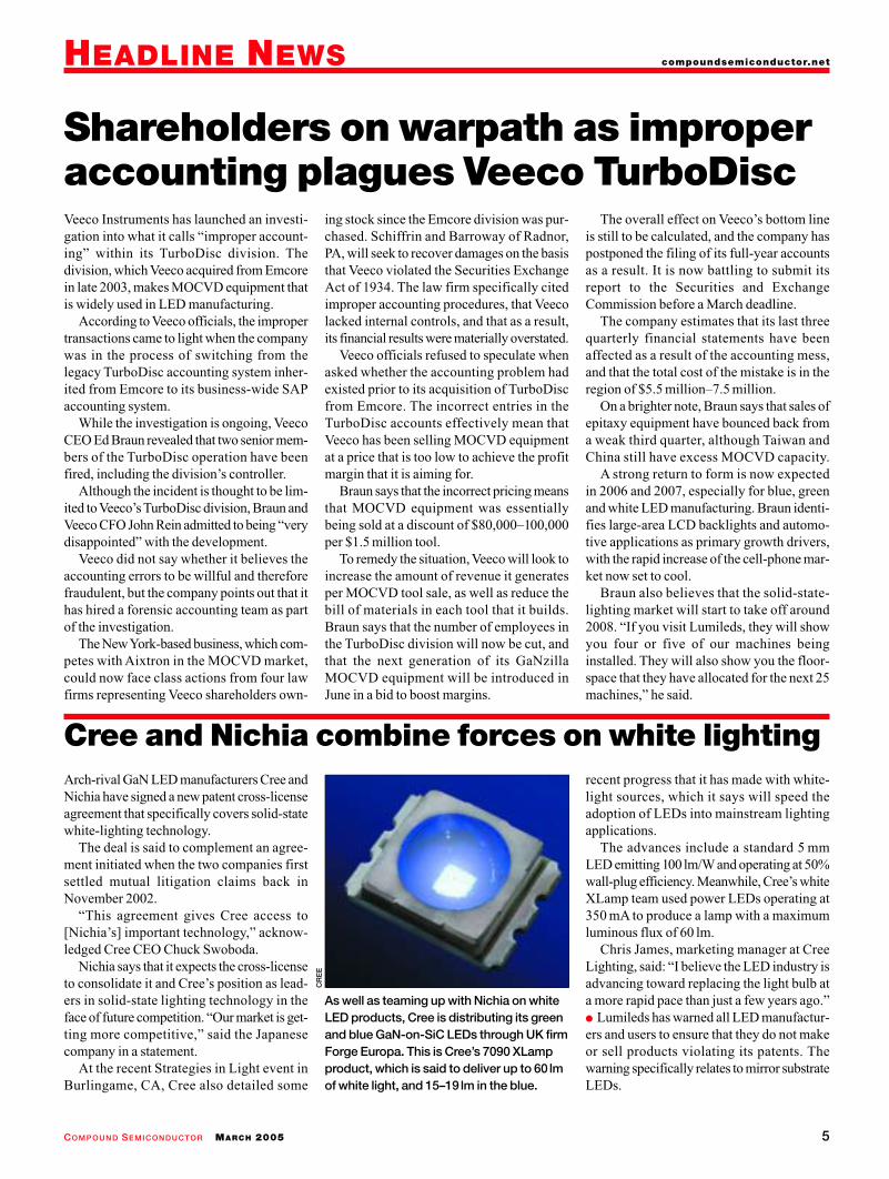
The advances include a standard 5 mmLED emitting 100 lm/W and operating at 50%wall-plug efficiency. Meanwhile, Cree’s whiteXLamp team used power LEDs operating at350 mA to produce a lamp with a maximumluminous flux of 60 lm.
Chris James, marketing manager at CreeLighting, said: “I believe the LED industry isadvancing toward replacing the light bulb ata more rapid pace than just a few years ago.” Lumileds has warned all LED manufactur-ers and users to ensure that they do not makeor sell products violating its patents. Thewarning specifically relates to mirror substrateLEDs.
Cree and Nichia combine forces on white lighting
As well as teaming up with Nichia on whiteLED products, Cree is distributing its greenand blue GaN-on-SiC LEDs through UK firmForge Europa. This is Cree’s 7090 XLampproduct, which is said to deliver up to 60 lmof white light, and 15–19 lm in the blue.
CR
EE
Infineon Technologies has agreed to sell partof its fiber-optic business to US-based Finisar,just weeks after trashing the original deal tosell the entire unit.
The revised agreement involves Finisarissuing Infineon some 34 million shares,valued at $50 million, in exchange forInfineon assets associated with the design,development and manufacture of opticaltransceiver products. The acquisition givesInfineon a 13% stake in Finisar.
Infineon says that 350 of its staff associatedwith the fiber-optic business will leave the firm,from sites in Berlin and Munich in Germany,and Longmont in the US. They will not betransferred to Finisar through the acquisition.
Finisar will acquire 10 Gbit/s transceiverdesigns for XPAK, X2, XENPAK and XFPform factors. Infineon will retain its com-ponents division for parallel optics and
fiber-to-the-home applications, and plasticoptical fiber products that are used in the auto-motive industry.
Infineon had previously withdrawn from a$200 million agreement to sell Finisar itsentire fiber-optic business unit. Both firmsthen appeared to be heading for the courts, butsince striking this new pact Infineon andFinisar have called off any legal action.
“The acquisition considerably broadensour customer and product portfolio, particu-larly our 10 Gbit/s product platforms,” saidFinisar’s CEO, Jerry Rawls.
Infineon’s CEO, Wolfgang Ziebart, indi-cates that more changes are on the way for theGerman outfit. “The transition supports theongoing consolidation of the fiber optic mar-ket, and is the first major step toward therestructuring of our fiber-optics group in orderto return to profitability.”
HEADLINE NEWS compoundsemiconductor.net
COMPOUND SEMICONDUCTOR MARCH 20056
Finisar and Infineon agreeon revamped fiber deal
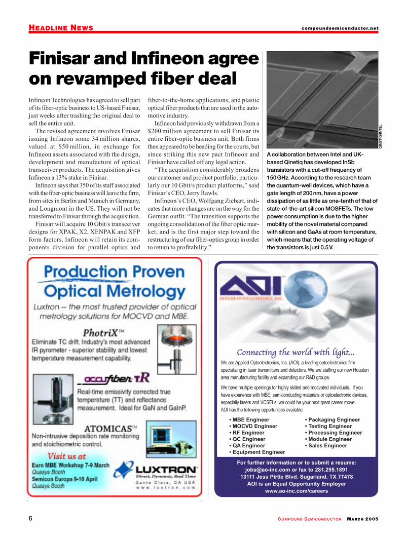
A collaboration between Intel and UK-based Qinetiq has developed InSbtransistors with a cut-off frequency of150GHz. According to the research teamthe quantum-well devices, which have agate length of 200nm, have a powerdissipation of as little as one-tenth of that ofstate-of-the-art silicon MOSFETs. The lowpower consumption is due to the highermobility of the novel material comparedwith silicon and GaAs at room temperature,which means that the operating voltage ofthe transistors is just 0.5V.
QIN
ET
IQ/I
NT
EL
NEW TO COMPOUND SEMICONDUCTOR WEEK 2005
THE KEY CONFERENCENovember 1–2, 2005
DATES FOR YOUR DIARYCOMPOUNDSEMICONDUCTORWEEK 2005
October 30 – November 2, 2005Compound Semiconductor Week is the annual meeting place for the compoundsemiconductor industry. Encompassing the 2005 IEEE Compound Semiconductor ICSymposium (CSICS), the Compound Semiconductor Manufacturing Expo (CS-MAX2005), the Key Conference and an exhibition showcasing suppliers of equipment andmaterials, it provides the ideal opportunity for your company to network across all levelsof the supply chain – in one great location.
For the first time The Key Conference will run alongside the other events inCompound Semiconductor Week 2005. This event is an executive-level meeting thatwill focus on the key technological themes and market trends that will dominate thefuture of the compound semiconductor industry. It is a must for senior managementwho appreciate how vital it is to gain an in-depth understanding of key marketdevelopments and competitor strategies.
To request more information please visit our website: www.compoundsemiconductor.net /csmax
October 30 – November 2, 2005 Palm Springs, California, USA
WHO SHOULD ATTEND?SENIOR CORPORATE MANAGERS/MARKET
ANALYSTS
COMPOUNDSEMICONDUCTORWEEK 2005
October 30 –November 2, 2005Palm Springs,California, USA
COMPOUND SEMICONDUCTOR MARCH 20058
Cell-phone unit sales are set to hit the 700mil-lion mark in 2005, but the market will growat a much slower rate than in the past twoyears. That’s the conclusion reached by botha report from IC Insights, a market-researchfirm based in Scottsdale, AZ, and Nokia, themarket-leading phone maker.
Cell phones are the single biggest applica-tion area for GaAs IC devices and LEDs.
Last year saw the fastest market growthin unit sales of cell phones since 2000, accord-ing to the report. Total shipments rose 29% in2004 to reach 670 million. But growth in 2005will be much slower, with the market expand-ing 5% and 705 million phones being sold, ICInsights predicts. Nokia estimates the 2004figure to be somewhat lower, but is predict-ing 10% growth this year.
However, the long-term forecast from ICInsights shows that the rate of growth will thenincrease every year through 2008. As a result,2008 will see shipments of more than one bil-
lion handsets, claims the report.The replacement market will become
increasingly important in the future, and hand-set makers will need to convince subscribersto invest in the latest technology with thenewest features to maintain overall marketgrowth. While 63% of phones sold in 2004were replacements, this figure is expected torise to 81% in 2008.
Camera phones have driven the replace-ment market in the past couple of years, reviv-ing the overall sector after it suffered its onlyyearly decline back in 2001. Since then, thenumber of phones sold per year has doubled.
IC Insights fully expects that consumerswill continue to be won over by new tech-nologies and functions, and predicts that theaverage time before a cell phone is replacedwill drop to just 30 months in 2008.
The market’s compound annual growth rate– in terms of units sold – will be 16% over the2001–2008 period, IC Insights concludes.
Slowing phone market totop 700m units in 2005
Filtronic, a UK microwave subsystems manu-facturer with a 6 inch GaAs fab, is enjoyingincreased demand for its products.
In its half-year financial report, the com-pany highlighted rapid growth in demand forpower amplifiers (PAs) bound for 3G hand-sets, as well as in low-cost transceivers forpoint-to-point microwave links.
Filtronic has also signed a supply agreementthat will see it become RF Micro Devices’number-one supplier of GaAs PHEMTs.Filtronic will make the components at its wafer-processing facility in Newton Aycliffe, UK.
Volume production is scheduled to beginin Q2 with the PHEMTs set to be incorporatedinto RFMD modules destined for cell-phonehandset and wireless LAN applications.
Filtronic says that its improved product mixshould lead to revenue growth in its compoundsemiconductor unit as this year unfolds,although it admits that chip manufacturing hasbeen adversely affected by some customerdelays in orders for volume production.
But with the PHEMT supply order,
increased demand for more complex, higher-value MMICs, and more foundry activity forhandset and wireless infrastructure OEMs,Filtronic has succeeded in broadening its cus-tomer base for GaAs devices.
Company chairman David Rhodes saysthat after what has been a tricky period finan-cially, the company can now take advantageof strengthening markets for wireless infra-structure and US defense.
Recently, Filtronic won a contract to up-grade US military aircraft, and a second PAproduct should be launched soon as the firmtargets 3G applications. “The W-CDMAmar-ket for PAs is considered to be showing 20%compound annual growth,” said the company.
However, Filtronic is not going ahead withthe planned initial public offering of its hand-set-products division, “in light of market con-ditions”. The division is focused on antennaproducts rather than semiconductor chips.
Overall, Filtronic posted an after-tax profitof £1.7 million on revenue of £130 million forthe six months ended November 30, 2004.
Filtronic is upbeat on prospectsas it signs PHEMT supply deal
GAAS & WIRELESS NEWS
SiCrystal AG - Paul-Gossen-Str. 100D-91052 Erlangen - [email protected] - fax: +49 9131 734952phone: +49 9131 734984 / +49 9131 734363
ll!
Ca usr ous
Cu i?
9COMPOUND SEMICONDUCTOR MARCH 2005
GAAS & WIRELESS NEWScompoundsemiconductor.net
Agilent Technologies has increased its focuson the mobile-handset market with the launchof the Agilent Asia Mobile DevelopmentCenter in Seoul, Korea.
The center will initially employ 50 staff,including the engineering team from Seoul-based Wavics, a fabless designer of ICs forpower amplifier (PA) applications. Agilentacquired Wavics in February.
Work at the center will focus on Agilent’smobile-handset components, including PAsfor CDMAand W-CDMA. As well as hostingresearch activity, the base will provide mar-keting and applications support.
One of the center’s aims is to create front-end modules that can integrate Agilent’s PAs
with its film bulk acoustic resonator duplexers.According to Agilent this combination will
allow phone manufacturers to significantlyreduce circuit-board space, enabling smallerand thinner clamshell-style handsets.
“Korea is a mobile technology leader, andits universities are graduating large numbersof highly educated and skilled electricalengineers,” said Young Sohn, president ofAgilent’s semiconductor products group.
“We chose Korea because it places us closeto our mobile-handset customers, where wecan better serve them and help define tomor-row’s innovative, feature-rich handsets.” See “Agilent sets out its consumer visionfor future profitability”, p28.
Agilent carves out mobileresearch base in Korea
20-year-old NATO aircraft are to have somesystems back-fitted with GaAs-based low-power amplifiers in a program that will helpto extend the service life of the fleet.
US-based Endwave will initially developprototype devices at its Sunnyvale, CA, head-quarters, while low-rate production is slatedto begin next year at the company’s newdefense systems division.
The $0.5 million development contractshould see the delivery of prototypes towardthe end of this year. Production will then begin
in 2006, assuming successful field qualifi-cation testing and subsequent authorization.
Amplifier production will take place inDiamond Springs, CA, at the firm’s manu-facturing center of excellence, and is expectedto run for between two and four years.
Chip fabrication will likely take place atNorthrop Grumman’s foundry, with whichEndwave has a strategic alliance.
Endwave recently consolidated its existingdefense product division with that of JCATechnology, a company that it acquired fromBookham Technology in July last year, toform Endwave Defense Systems. The divi-sion is retaining the JCA brand name for itsRF amplifier modules, which is the key tech-nology behind its products.
Endwave bagsdefense deal
RF Micro Devices has shrunk its GaAsHBT PowerStar power amplifier (PA)modules by 30%. The firm showed off thetwo new products in the PowerStar familyat the 3GSM World Congress event inCannes, France, last month. Both modulesfeature integrated battery voltage trackingcircuitry, which is said to be an industryfirst for standard PA modules. Xindium Technologies, a US firm that isdeveloping advanced RF devices for mobilephones, has introduced a new PAmodulebased on InGaP HBT technology. Xindiumsays that its product gives handset builders
greater diversity in their supplier base. Californian GaAs device manufacturerCeleritek made revenue of $2.8 million inits most recent quarter, following the sale ofits defense subsystem business to Teledynelast October. That sale netted the firm$31.4 million, and as a result Celeritek gaveout a cash dividend of $3 per share to everyshareholder – totaling $38.9 million. Agilent Technologies introduced anE-PHEMT low-noise amplifier suitable forthe 0.5–6 GHz frequency range, includingwireless LAN, WiMAX point-to-multipoint systems and cordless phones.
In brief
GAAS & WIRELESS NEWS compoundsemiconductor.net
COMPOUND SEMICONDUCTOR MARCH 200510
Leading cell-phone maker Nokia has pre-dicted a massive uptake of 3G wireless ser-vices this year. It believes that the number ofsubscribers to wideband code division multi-ple access (W-CDMA) will more than quadru-ple to 70 million in 2005.
The Finnish company is also very bullishon overall subscriber growth, forecasting thatthe global base will rise to 2 billion this yearand on to 3 billion by 2010.
Nokia’s forecast came at the 3GSM WorldCongress, the annual mobile jamboree heldin Cannes on the French Riviera.
“We expect to see widespread commer-cialization of 3G W-CDMAnetworks duringthe year,” said Simon Beresford-Wylie,Nokia’s executive vice-president of networks.“With more than 100 3G networks opened bythe end of 2005, Nokia is projecting a sharprise in the number of 3G subscribers, to70 million by the end of the year.” Only16 million subscribers signed up to 3G ser-vices in 2004, adds Beresford-Wylie.
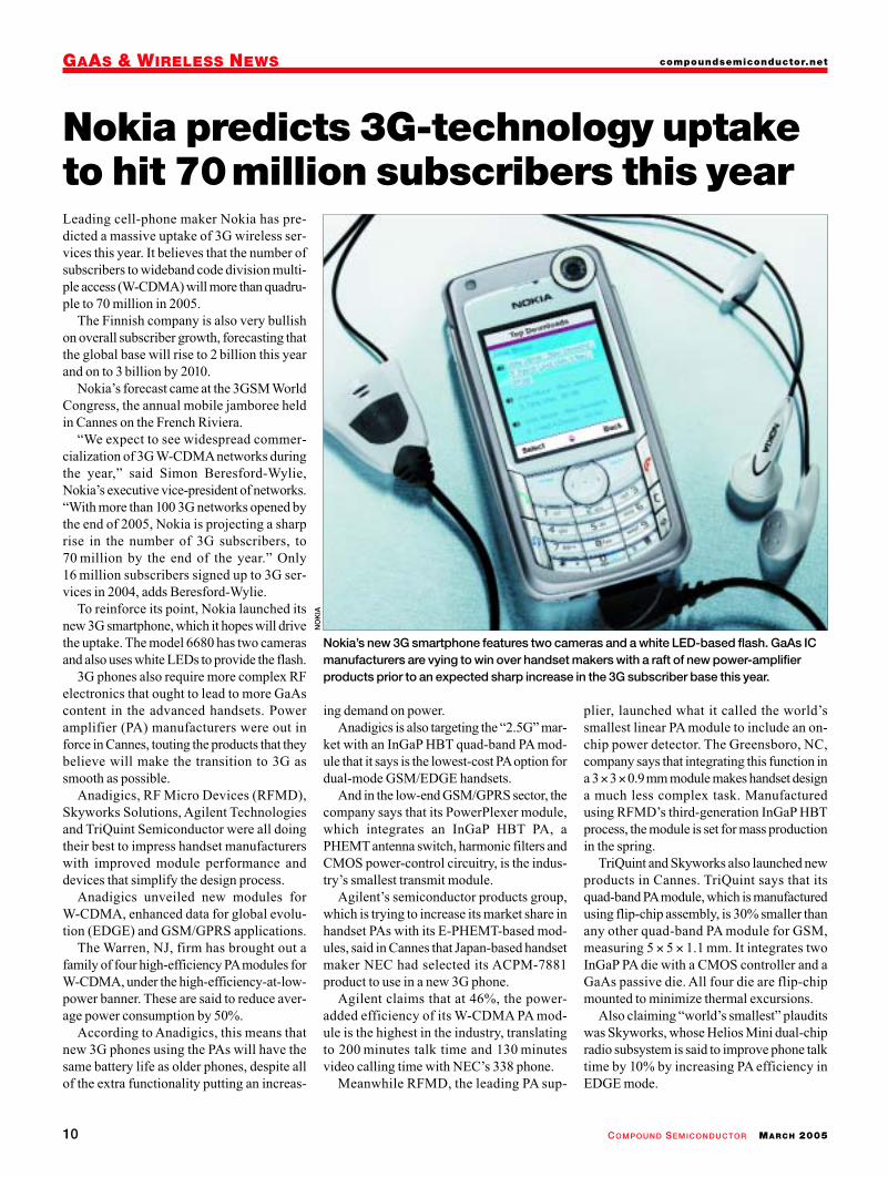
To reinforce its point, Nokia launched itsnew 3G smartphone, which it hopes will drivethe uptake. The model 6680 has two camerasand also uses white LEDs to provide the flash.
3G phones also require more complex RFelectronics that ought to lead to more GaAscontent in the advanced handsets. Poweramplifier (PA) manufacturers were out inforce in Cannes, touting the products that theybelieve will make the transition to 3G assmooth as possible.
Anadigics, RF Micro Devices (RFMD),Skyworks Solutions, Agilent Technologiesand TriQuint Semiconductor were all doingtheir best to impress handset manufacturerswith improved module performance anddevices that simplify the design process.
Anadigics unveiled new modules forW-CDMA, enhanced data for global evolu-tion (EDGE) and GSM/GPRS applications.
The Warren, NJ, firm has brought out afamily of four high-efficiency PAmodules forW-CDMA, under the high-efficiency-at-low-power banner. These are said to reduce aver-age power consumption by 50%.
According to Anadigics, this means thatnew 3G phones using the PAs will have thesame battery life as older phones, despite allof the extra functionality putting an increas-
ing demand on power.Anadigics is also targeting the “2.5G” mar-
ket with an InGaP HBT quad-band PA mod-ule that it says is the lowest-cost PAoption fordual-mode GSM/EDGE handsets.
And in the low-end GSM/GPRS sector, thecompany says that its PowerPlexer module,which integrates an InGaP HBT PA, aPHEMT antenna switch, harmonic filters andCMOS power-control circuitry, is the indus-try’s smallest transmit module.
Agilent’s semiconductor products group,which is trying to increase its market share inhandset PAs with its E-PHEMT-based mod-ules, said in Cannes that Japan-based handsetmaker NEC had selected its ACPM-7881product to use in a new 3G phone.
Agilent claims that at 46%, the power-added efficiency of its W-CDMA PA mod-ule is the highest in the industry, translatingto 200 minutes talk time and 130 minutesvideo calling time with NEC’s 338 phone.
Meanwhile RFMD, the leading PA sup-
plier, launched what it called the world’ssmallest linear PA module to include an on-chip power detector. The Greensboro, NC,company says that integrating this function ina 3×3×0.9mm module makes handset designa much less complex task. Manufacturedusing RFMD’s third-generation InGaP HBTprocess, the module is set for mass productionin the spring.
TriQuint and Skyworks also launched newproducts in Cannes. TriQuint says that itsquad-band PAmodule, which is manufacturedusing flip-chip assembly, is 30% smaller thanany other quad-band PA module for GSM,measuring 5 × 5 × 1.1 mm. It integrates twoInGaP PA die with a CMOS controller and aGaAs passive die. All four die are flip-chipmounted to minimize thermal excursions.
Also claiming “world’s smallest” plauditswas Skyworks, whose Helios Mini dual-chipradio subsystem is said to improve phone talktime by 10% by increasing PA efficiency inEDGE mode.
Nokia predicts 3G-technology uptaketo hit 70million subscribers this year
Nokia’s new 3G smartphone features two cameras and a white LED-based flash. GaAs ICmanufacturers are vying to win over handset makers with a raft of new power-amplifierproducts prior to an expected sharp increase in the 3G subscriber base this year.
NO
KIA
OPTO NEWS compoundsemiconductor.net
COMPOUND SEMICONDUCTOR MARCH 2005 11
Booming sales of DVD players and driveswill spur the market for AlGaInP laser diodesto $1.5 billion by 2009, according to a newreport from Strategy Analytics.
The current market, estimated to be wortharound $970 million, is dominated by Japan-ese firms such as Sony, Sharp, Mitsubishi andMatsushita, with a market share of about 75%between them. Samsung in Korea is anothermajor producer, while a handful of Chinese andTaiwanese companies make up the remainder.
While the market will grow at around 7%annually through 2009, stiff competition fromnew entrants in China and Taiwan will meanthat an increasing proportion of the deviceswill be made in South East Asia rather thanJapan. “Commodity LED production hasalready moved from Japan to lower-cost coun-tries,” said Asif Anwar, the director of StrategyAnalytics’ GaAs service. “Taiwanese andChinese manufacturers will press for a simi-lar migration of laser-diode production andcompete on price.”
This trend can be observed at HuaguangOptoelectronics, mainland China’s largestdomestic producer of 650 nm laser-diodechips, which is planning to double productioncapacity this year. Currently manufacturingaround 10 million chips per month, the com-pany says that it will invest in processingequipment to increase output of the red lasers,which are used in DVD applications, laserpointers and barcode scanners.
Huaguang, which also makes a range ofyellow and red LEDs, started red-laser pro-duction two years ago, and chief technologyofficer Xiangang Xu believes that the com-pany has a market share of 50–60% in main-land China. Xu says that products are basedon proprietary technology developed atShandong University.
Despite the drive toward cheaper produc-tion, Anwar does not a see a major switchaway from Japanese manufacturers in theshort term, however. He expects that sometechnical challenges in the design of deviceswill require the attention of established ven-dors, and that this will slow the progressionto lower-cost sites. These design challengesinclude making the chips suitable for high-temperature operation so that they can be usedfor faster DVD burning.
Indeed, production capacity for high-powerlasers used to write data in DVD recorders isexpected to double at Japan-based MitsubishiElectric. According to the Nihon KeizaiShimbun newspaper, the company, which isbelieved to have a 70% share of the globalmarket for such devices, will invest $20 mil-lion – 30 million at its Hyogo manufacturingbase in a bid to raise production volume to10 million units per month by September.
Mitsubishi previously ramped productionfrom 1.5million to 3.5million units per monthin December 2003, and then to 5 million unitsper month last spring.
By Jacqueline Hewett in San JoseWith mass production of high-power pulsedand low-power continuous-wave (CW)405 nm lasers set to begin in a couple ofmonths, Nichia is working to develop similardevices emitting in the ultraviolet and theblue–green. Such devices should be useful forbiological, medical and display applications.
Reporting on progress at the recent Pho-tonics West conference in San Jose, CA,Nichia researchers told delegates about a newLED structure with an increased aluminumcontent that emits at 365 nm, the same wave-length as its commercial i-LED.
The structure consists of an AlInGaN sin-gle quantum well layer, with Al0.13Ga0.87N/
Al0.09Ga0.91N cladding regions and anAl0.065Ga0.935N waveguide. The laser, whichhas an expected lifetime of 2000 h, works inCW mode at room temperature, with a thresh-old current of 50 mA at 4.8 V.
Progress in the blue–green region has beenless significant because of the poor crystal qual-ity of the InGaN active layer. Nichia said thatit was proving difficult to make 485 nm lasers.The best result achieved so far is a 482nm laserwith 5mWcontinuous operation at room tem-perature, which is said to be the longest-wave-length laser diode based on GaN yet made.
Jacqueline Hewett is technology editor ofOptics.org and Opto & Laser Europe magazine.
Bookham Technology and nLight havelaunched high-power laser diodes that targetapplications including materials processing,medical treatment, and act as pump sourcesfor other solid-state, fiber and disk lasers.
Bookham’s 120 W multimode laser, whichwas developed at its Zurich, Switzerland,facility, is claimed to be the most powerfulcommercially available continuous-wave(CW) laser-diode bar in the world. Standardproducts emit at 915, 940 and 980 nm.
“We are confident that the high brightnessand reliability of our industrial laser-diodebars will continue to attract new customersand accelerate the growth of diode-pumpedlaser systems,” remarked Greg Smolka, Book-ham’s vice-president of sales and marketing,commercial products.
Bookham’s laser-diode bar is suitable forapplications as diverse as multimode pump-ing of cable-TV amplifiers, optical pumpingfor frequency-doubled lasers operating in thevisible range, marking and printing, hairremoval, and intersatellite communication.
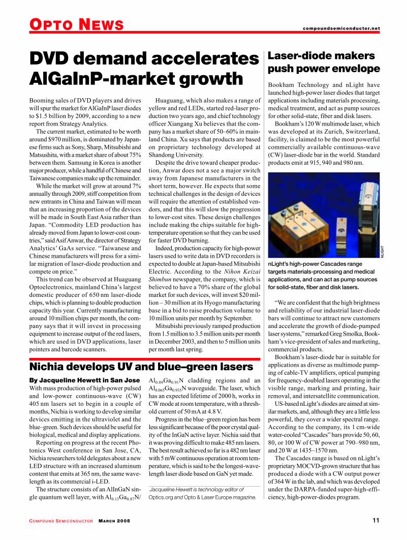
US-based nLight’s diodes are aimed at sim-ilar markets, and, although they are a little lesspowerful, they cover a wider spectral range.According to the company, its 1 cm-widewater-cooled “Cascades” bars provide 50, 60,80, or 100 W of CW power at 790–980 nm,and 20 W at 1435–1570 nm.
The Cascades range is based on nLight’sproprietary MOCVD-grown structure that hasproduced a diode with a CW output powerof 364 W in the lab, and which was developedunder the DARPA-funded super-high-effi-ciency, high-power-diodes program.
DVD demand acceleratesAlGaInP-market growth
Nichia develops UV and blue–green lasers
Laser-diode makerspush power envelope
nLight’s high-power Cascades rangetargets materials-processing and medicalapplications, and can act as pump sourcesfor solid-state, fiber and disk lasers.
NLI
GH
T
LED NEWS compoundsemiconductor.net
COMPOUND SEMICONDUCTOR MARCH 200512
By Michael HatcherKopin Corporation has formed a joint venturecompany to spin off its LED technology to alow-cost manufacturing operation in Asia.
The Taunton, MA, firm will take a share inKo-Brite Corporation in return for its techni-cal knowledge relating to InGaN LED pro-duction and a $3 million investment.
In addition to Kopin’s investment, venture-capital group WK Technology Fund, Taiwan-based Kopin subsidiary KTC, and LEDpackaging company Bright LED have com-mitted $11.5 million to the project.
The initial deal puts only a small value onKopin’s InGaN technology, but the US firmstands to receive $7.5 million by providingtraining services and transferring equipmentto Ko-Brite. Overall, the transfer is expectedto net Kopin around $3 million.
Under the deal, GaN-materials-growthcapability will be established in Taiwan, alongwith die-production facilities near Hong Kongin mainland China. Ko-Brite will market thepackaged LEDs globally.
Kopin has been trying to find a low-costLED-manufacturing partner to pair with itstechnology for some time. It made the deci-sion to switch to a different manufacturingstructure after LED prices, in particular for blue
cell-phone backlights, plummeted in 2003,thanks largely to low-cost Asian chip makers.
“Current trends affecting the LED indus-try clearly indicate that successful participantswill need both leading-edge technology anda competitive cost structure,” said John Fan,Kopin’s CEO. He claims that the best busi-ness model for LED manufacturing is to per-form epitaxy in Taiwan and labor-intensivepackaging in mainland China. He believes thatChina provides the biggest market for solid-state lighting applications of LEDs.
“This joint venture...will position Ko-Briteas a technology leader with a strong manage-ment team and one of the lowest manu-facturing cost structures in the industry,” saidFan. He adds that Kopin had decided to forma joint venture, rather than establish an Asiansubsidiary to make its LEDs, partly becauseit would allow the company to focus on its tworemaining core products – HBT wafers andmicrodisplay technology.
Kopin plans to stop the costly exercise ofmanufacturing LEDs itself by March 31, andis aiming to have completed training andtransfer of its LED operations to Ko-Brite byJuly 1. The production transfer will leave oneof Kopin’s two manufacturing sites in the US90% empty and probably up for sale.
Kopin sets up InGaN LED-production venture in Asia
By Richard Stevenson inBurlingameThe market for high-brightness LEDs grewby 37% in 2004 to reach $3.7 billion. That’saccording to Bob Steele, who opened lastmonth’s Strategies in Light 2005 conferencein Burlingame, CA.
Once again, applications in mobile ter-minals dominated HB-LED sales. Cell phonesand their like accounted for 58% of the mar-ket ($2.15 billion), followed by 13% sharesfor automotive and signage applications.
According to Steele, the application ofwhite LEDs in full-color-display backlight-ing enjoyed 75% market growth in 2004. Infact, LCD backlighting overtook keypadbacklighting as the biggest sector for HB-LEDs in mobile appliances, and was worth48% of the $2.15billion market. In 2003, LCDbacklights represented 42% of this market.
Keypad backlights represented 38% of themobile-appliance market for HB-LEDs in2004, down from 45% in the previous year.
In automotive applications, center high-mounted stop lamps continued to show mod-est growth. European sales of these productsare now beginning to saturate, with an esti-mated market penetration of more than 80 %.
Steele believes that in 2004 the largestgrowth in epitaxy and chip processing activ-ity took place in Asia. However, he also notedthat overcapacity in the region has led to severeprice pressure, especially in low- to mid-rangeapplications such as keypad backlights.
Looking ahead, Steele predicts that the HB-LED market will nearly double by 2009,increasing to a value of around $7 billion.Strong though this growth is, it represents aslow-down compared with the tremendouslyfast expansion seen between 1999 and 2004.
HB-LED market will be worth $7bn by 2009
Rajiv K.Agarwal,Ph.D.LeadResearchEngineer
Higher background levels ofn type dopants in GaAs andAlGaAs structures are causedby trace levels of germanium,
silicone and sulfur species present in the arsine.As customer applications evolve, the purityrequirements for arsine must as well. Untilrecently, background doping levels of 1015/cm3
were considered acceptable in most applica-tions. In general, most currently available high-purity grades of arsine can satisfy these require-ments. However, process changes and demandfor more sophisticated devices have resultedin the need for lower background doping levels.To address these more stringent requirements,Air Products is introducing MegabitTM IIIarsine, our purest grade available. Our newMegabit III arsine has significantly reduced theamounts of germanium, silicon and sulfur spe-cies. Testing done at an independent laboratoryproved the effectiveness of Megabit III on thickgallium arsenide films, with excellent results.In all cases, the background doping level was<<1014/cm3. Our research has shown thatAir Products’ Megabit III arsine will performmore consistently and produce fewer defectsin our customers’ finished products.
For more information or to submit aquestion for "Ask the Expert," visit us atwww.airproducts.com/AsktheExpert or callus at (800) 654-4567 or (610) 706-4730 andmention code #144.
© Air Products and Chemicals, Inc., 2004 (24061) LCS-1
tell me morewww.airproducts.com/AsktheExpert
Ask the Expert
I am experiencing highn type backgrounddoping levels in myMOCVD process when Igrow GaAs and AlGaAsdevices. I think theproblem is in the arsineI use. I’m buying the bestgrade available. Whatcan I do?
A
Q
13COMPOUND SEMICONDUCTOR MARCH 2005
LED NEWScompoundsemiconductor.net
By Tim WhitakerIII-N Technology, a company located inManhattan, Kansas, has developed single-chip power AC-LED lamps that can beplugged directly into standard power outletsand lamp sockets without power conversion.The company has applied for patent protec-tion covering its invention.
While standard power LEDs operate froma DC supply with a voltage of around 3.5V(forblue devices), the new chips are capable ofoperating directly from an AC supply with avoltage of 110V(in the US) or 220V(in Asia).
The announcement was made at thePhotonics West conference on January 26 byHongxing Jiang, who founded III-N Tech-nology with fellow Kansas State Universityprofessor Jingyu Lin.
III-N Technology says that its AC-LEDswere demonstrated to the US Department ofDefense community in a forum held in May2004 in Reston, VA.
Seoul Semiconductor unveiled a similartechnology at a press conference in Koreaaround the same time that III-N made itsannouncement.
III-N Technology’s invention came out ofthe micro-LED array technology devised bythe same team and which featured on the coverof Compound Semiconductor in November2000. The micro-LED array consists of sev-eral tens of nitride LED devices fabricated ona single semiconductor chip. The emitters canbe individually addressed so that the chip acts
as a multipixel microdisplay.III-N Technology has further developed the
manufacturing technology to fabricate arraysof emitters linked in series by on-chip inter-connects. The number of linked emitters ischosen so that the sum of the voltage dropacross the individual emitters adds up to thevoltage of the AC supply.
Since LEDs only emit light when they areforward biased, two arrays are created, one ofwhich lights up during the first half-cycle ofthe AC power source. The second array lightsup when the polarity of the source is reversed.It is also possible to use a single array and ahigh-voltage DC source, if required.
The technology eliminates the need for anAC/DC power converter, which is expectedto lead to significant cost savings, while thechip-level architecture could lead to improve-ments in efficiency compared with single-chiphigh-power LEDs. The main advantage, how-ever, is its compatibility with the existinglighting and electricity infrastructure.
III-N Technology says that its power AC-LEDs have comparable luminous efficiencyto existing DC power LEDs of the same chipsize. Hongxing Jiang says that the companyis seeking to license its technology to manu-facturers of DC power LEDs, and that thechip-fabrication technology is fully compat-ible with DC power LED production lines.
Tim Whitaker is editor of LEDs Magazine, seewww.ledsmagazine.com.
III-N Technology unveils novelsingle-chip power AC-LED lamp
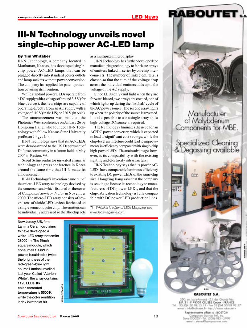
New Jersey, US, firmLamina Ceramics claimsto have developed awhite-LED array that emits28000 lm. The 5 inchsquare module, whichconsumes 1.4kW inpower, is said to be twicethe brightness of thered–green–blue lightsource Lamina unveiledlast year. Called “AterionWhite”, the array contains1120 LEDs. Itscolor-correctedtemperature is 5500K,while the color renditionindex is rated at 80. LA
MIN
A C
ER
AM
ICS
FIBER NEWS compoundsemiconductor.net
COMPOUND SEMICONDUCTOR MARCH 200514
US firm Vitesse Semiconductor and Ireland’sEblana Photonics have applied a standardHBT manufacturing process to fabricate laserchips on Vitesse’s 4 inch InP wafer line.
The two companies have also signed amanufacturing agreement, and Eblana is plan-ning to start ordering materials and fabrica-ting chips around the middle of this year.
Vitesse and Eblana believe that the low-cost process, which avoids the costly regrowthsteps normally used in laser fabrication,demonstrates that optoelectronic chips can bemade in very high volumes in a way that imi-tates silicon IC manufacture.
Eblana CEO James O’Gorman says thatconventional laser fabrication is totallyunsuited to very-high-volume manufacturing,and therefore only useful for niche applica-tions such as the long-haul market. He claimsthat his technology platform is suitable foraccess, metro and long-haul applications.
O’Gorman believes that with huge fiber-to-the-home build-out programs promised in
Japan and South Korea, as well as smallerdevelopments in progress in the US currently,there is a need for low-cost, high-volumelaser-manufacturing technology. “This is aonce-in-a-lifetime infrastructure build-out,”O’Gorman told Compound Semiconductor.
The performance of the lasers fabricatedon Vitesse’s 4 inch InP foundry line is said tobe as good as those made using distributedfeedback technology. The singlemode lasersemit at 1.54 µm, with a threshold current of12mA. The sidemode suppression ratio is bet-ter than 40 dB, with a 20 mW laser output.
Eblana’s technology, developed byO’Gorman and others at Trinity CollegeDublin and the Irish National Microelec-tronics Research Center in Cork, uses “pho-ton-mode engineering” to control laser modes.
This means that after growing the laser’sepitaxial layers, the wafer is structured to formphotonic bandgaps that control the device out-put. Because there is no need to regrow semi-conductor heterointerfaces, claims Eblana,the technology is inherently cheaper to manu-facture and is more reliable than its rivals’.
“Since Eblana’s technology only uses stan-dard electronics design rules and matureprocesses, it achieves performance and prod-uct consistency typical of ICs, which to datehave not been a feature of photonics prod-ucts,” said Ray Milano, vice-president of opti-cal technologies at Vitesse.
Milano, who is not aware of any similarapproaches to laser production that avoid theregrowth step, adds that he sees no drawbacksto Eblana’s technology. “To my knowledge,nobody else has established this kind ofprocess flow,” he said.
Milano added that as well as being moremanufacturable, Eblana’s lasers also had someadvantages: “[Our] process, with its pho-tolithographically defined features, ends upproducing a tighter spread in wavelengths.”
Using Vitesse’s standard VIP-2 InP HBTprocess will reduce the overall cost of trans-ceiver manufacture by more than 50% in vol-ume applications, claims Eblana.
O’Gorman says that Eblana is in discus-sions with potential customers and has bookedfoundry time with Vitesse. He adds that thecompany hopes to be ordering the necessarymaterials by the middle of this year.
Eblana, founded in late 2000, had raised atotal of $7.75 million after it closed its SeriesB funding round in February 2003.
Think that epi-ready sapphire waferis defect free? Think again.
Detect and classify those critical transparent wafer defects with Candela.™ Our CandelaOptical Surface Analyzers are unique surface inspection systems that automaticallydetect and classify defects on transparent materials like sapphire, SiC, LiNbO3, and glass.Faster than operator-dependent microscope inspection, these systems can detect surfacecontaminants and defects on wafer substrates that hurt device performance. Measures scattered light, reflected light, phase shift, and surface topography Detects and classifies epi and coating defects Accommodates 50 to 200 mm wafers Manual or cassette-to-cassette operation For more product information, go to: www.kla-tencor.com/candela
Accelerating Yield®
©20
05 K
LA-T
enco
r Cor
pora
tion.
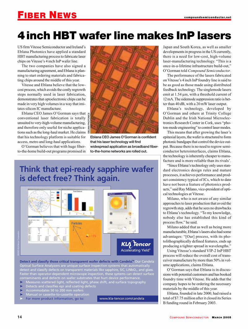
Eblana CEO James O’Gorman is confidentthat his laser technology will findwidespread application as broadband fiber-to-the-home networks are rolled out.
4inch HBT wafer line makes InP lasers
EB
LAN
A P
HO
TO
NIC
S
15COMPOUND SEMICONDUCTOR MARCH 2005
FIBER NEWScompoundsemiconductor.net
BinOptics, the US company that makesetched-facet lasers, has raised $10 million inSeries B funding.
The company says that it will use themoney to scale up its production capabilityfor its existing InPproducts, while it also plansto target the emerging next-generation DVDmarket with blue diode lasers based on GaN.
“BinOptics has shown that its etched-facettechnology is advantageous for a wide rangeof semiconductor materials,” said Dan Brown,a partner at ArrowPath Venture Capital, oneof two new investors in the company that ledthe funding round.
Greg Hulecki, managing partner at the sec-ond new investor, FA Technology Ventures,added: “BinOptics will play a significant rolein reducing the cost of its customers’ equip-ment and systems through efficient manu-facturing and functional integration.” Huleckisays that BinOptics will now move its prod-ucts to full-scale production.
Those products include the proprietaryhorizontal-cavity surface-emitting laser
(HCSEL) – a chip technology that integratesa horizontal laser cavity with a 45° etchedreflecting mirror to direct the beam vertically(Compound Semiconductor July 2004 p14).
Unlike most laser fabricators, which use acleaving technique to create laser facets,BinOptics uses etching. This means that a dis-tributed Bragg reflector can be used insteadof an optical coating to produce high reflec-tion of the laser light.
BinOptics’ InP-based HCSELs emit atwavelengths of 1310 and 1550 nm, and thecompany plans to integrate these devices withhigh-speed detectors to create transceiverchips for passive optical networks. It expectsto have a commercial product available beforethe end of this year.
The etched-facet laser technology was firstdeveloped at Cornell University, and Bin-Optics remains based at the nearby CornellBusiness and Technology Park in Ithaca, NY.
The firm was founded in 2000 with fund-ing from Draper Fisher Jurveston, CayugaVenture Fund II and Stanford University.
BinOptics to scale up productionfollowing $10m funding scoop
JDS Uniphase’s communicationsbusiness is seeing solid growth as the fiber-optic market settles down. The group hasreported a sequential increase in revenuefor five consecutive quarters.
For its second quarter of fiscal 2005ending December 31, 2004, JDSU reportedtotal revenue of $180.5 million. Thecommunications group contributed$106.7 million, or 59% of this total. Theother $73.8 million came from thecompany’s commercial and consumerproducts group. For much of the past twoyears, the two product groups havereported roughly equal revenues. Californian optoelectronic chipmakerInPhenix has received ISO 9001:2000certification for its manufacturing ofoptoelectronic components and modules.The Livermore company owns a wafer fabthat produces GaAs and InP chips, where italso offers foundry services. Fiber module and InP chipmakerBookham Technology saw revenueincrease 5% sequentially to $45.8 million
in its second quarter, which ended January1, 2005. However, the company’s negativegross margin widened, something that thecompany attributed to the weakness of theUS dollar versus UK sterling.
Despite improving revenue, net losscame in at $41.1 million, compared withjust $10.6 million this time last year. Thefirm’s costs have escalated as it is runningtwo production lines while switching muchof its assembly operation to China. Emcore reported a 17% year-on-yearrevenue increase as it made sales of$27 million in its first fiscal quarter of 2005,which ended on December 31, 2004.Having cut some research and developmentcosts, the firm posted a loss of $9.1 million. Avanex, the US firm that acquired AlcatelOptronics in May 2003, posted a net loss of$24.4 million on revenue of $41.9 million inits second quarter, ended December 31,2004. Although the loss is slightly greaterthan that of the prior quarter, it represents asubstantial improvement on the$33.5 million net loss seen one year ago.
In Brief
Thomas SwanScientific Equipment
Thomas Swan Scientific Equipment LtdBuckingway Business ParkSwaveseyCambridge CB4 5FQ UK
t +44 (0)1223 519444f +44 (0)1223 519888e [email protected]
A member of the AIXTRON group of companies
• The Next Generation of an IndustryStandard: Epison 4 OM GasConcentration Analyser
• Improved accuracy, extended to lower concentration, better signal to noise ratio
• Optimised design – integrated ultrasonic cell and control unit
• DeviceNet and Profibus fieldbuscommunications for system integration
CIP’s sitIpswichpedigrecomponwas whresearcproductmonomwas parthat devfiber amalso insdevelopburied hAfter BTCorningcompanequipmdeparte
CIP w2004 aslaboratoboth indOwned Developnot-for-any incoreinvest
The C
compoundsemiconductor.net
COMPOUND SEMICONDUCTOR MARCH 200516
COMPONENT DEVELOPMENT
UK research center aims In late 2004 The Centre for Integrated
Photonics (CIP), an independent researchand development firm with a rich heritage
in InP-based optical components, released itsfirst products. Electro-absorption modulators(EAMs), which operate at either 1300 or1550 nm and at 10 or 40 Gbit/s, are the resultof a development program that began whenBritish Telecom (BT) owned the premises, andcontinued when Corning took over the site.
Today, however, CIP’s facility is owned bythe East of England Development Agency.Fitted out with £40 million ($74 million) ofinherited high-tech equipment, these facilitiesare used by the not-for-profit research organ-ization to develop products for both industryand academia. The firm has released its EAMspartly in a bid to raise its profile and stimulatecollaboration with industrial partners. Thecomponents themselves have useful charac-teristics, including low-voltage operation, highoptical throughput and high-power handling.
The key attribute of EAMs – devices whichare analogous with camera shutters – is thatthey generate short optical pulses at frequen-cies unattainable by laser modulation. Sincethey do not emit light, they are used in con-junction with a continuous-wave laser. Apply-ing an electric field across the device enablesrapid switching, thereby circumventing theslower electron-hole recombination process.Dave Moodie, CIP’s EAM specialist, said:“The speed is fundamentally limited by theuncertainty principle”, implying that thedevices could operate in the terahertz regime.
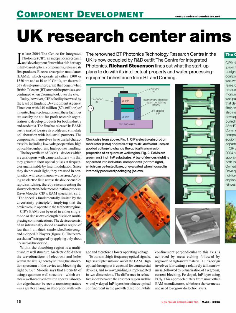
CIP’s EAMs can be used in either single-mode or dense-wavelength division multi-plexing communications. The devices consistof an intrinsically doped absorber region ofless than 1 µm thick, sandwiched between p-and n-doped InP layers (figure 1). The “cam-era shutter” is triggered by applying only about3 V across the device.
Within the absorbing region is a multi-quantum well structure. An electric field altersthe wavefunctions of electrons and holeswithin the wells, thereby shifting the absorp-tion spectrum of the device and blocking thelight output. Moodie says that a benefit ofusing a quantum well structure – which cre-ates a well-resolved exciton spectral absorp-tion edge that can be seen at room temperature– is a greater change in absorption with volt-
age and therefore a lower operating voltage.To transmit high-frequency optical signals,
light is coupled into and out of the EAM. Highoptical throughput is essential for commercialdevices, and so waveguiding is implementedin two dimensions. The difference in refrac-tive index between the absorber region and then- and p-doped InP layers introduces opticalconfinement in the growth direction, while
confinement perpendicular to this axis isachieved by mesa etching followed byregrowth of high-index material. CIP’s designinvolves fabricating a relatively tall, narrowmesa, followed by planarization of a regrown,current-blocking, Fe-doped, InP layer usingPCl3. This approach differs from most otherEAM manufacturers, which use shorter mesasand need to regrow dielectric layers.
The renowned BT Photonics Technology Research Centre in theUK is now occupied by R&D outfit The Centre for IntegratedPhotonics. Richard Stevenson finds out what the start-upplans to do with its intellectual-property and wafer-processing-equipment inheritance from BT and Corning.
p-dopedcap
quarternary absorberregion containing
MQWs
InP substrate
p-InP
n-InP
Fe-dopedInP
~VFe-doped
InP
Clockwise from above. Fig. 1. CIP’s electro-absorptionmodulator (EAM) operates at up to 40Gbit/s and uses anapplied voltage to change the optical transmissionproperties of its quantum well region. Fig. 2. EAMs aregrown on 2 inch InP substrates. A bar of devices (right) isseparated into individual components (bottom right),which can be tested bare, or evaluated when housed ininternally produced packaging (below).
CIP
17COMPOUND SEMICONDUCTOR MARCH 2005
COMPONENT DEVELOPMENTcompoundsemiconductor.net
Moodie says that CIP’s design has theadvantage of distributing optical absorptionmore gradually along the EAM’s length,which improves optical power handling. Theoptical mode between the EAM and the opti-cal fiber is also better matched, thereby reduc-ing coupling losses and resulting in low deviceinsertion losses (typically < 4.5 dB in the low-loss stage). Afurther advantage of this design
is the lower electrical capacitance per unitlength, allowing fabrication of high-speed(40 Gbit/s) EAMs. The end result is uncom-pensated 40 Gbit/s transmission in the1550 nm waveband over distances of up to100 km, a feat that usually requires an addi-tional optical amplifier.
Size is everythingThe size of the EAMs also gives them a com-petitive edge – tens of thousands of milli-meter-sized devices can be produced from a2 inch InP wafer. “Size is becoming a hugeissue,” said Moodie, who believes that estab-lished lithium niobate-based EAMs are toobulky to compete in tomorrow’s market-place.
CIP is targeting a range of applications withits high-speed EAMs, including optical modu-lators for low-chirp 10 Gbit/s systems,40 Gbit/s transmission, optical sampling anddemultiplexing for 160 Gbit/s optical timedivision multiplexing, and as compact opti-cal-pulse sources. The devices could also besuitable for more exotic networks, for instanceproviding RF-to-optical conversion in mili-tary, medical and sensor applications.
According to Moodie’s colleague AlastairPoustie, who investigates EAM performance,CIP is also able to produce variants of thedevice with application-specific characteris-tics designed to operate “anywhere across theInP band”. Poustie acknowledges that CIPrequires a partner for the large-volume manu-facture of EAMs, because although chip pro-duction can be carried out in-house, packagingwould have to be undertaken elsewhere. Thefirm, which can integrate EAMs with otheroptoelectronics, will also consider other agree-ments, such as licensing its process.
The cycle time for CIP to manufacture itsEAMs is currently around two weeks, thoughCIP’s III-V growth specialist MichaelRobertson says this could be speeded up byintroducing some automation.
The range of growth, processing, and testequipment that CIP owns, with a total valueof £40 million, is truly outstanding when oneconsiders its size. EAM material growth iscarried out by MOCVD on an Aixtron2400G3 system with an 8 × 2 inch platform,with the current focus on proof of concept,rather than manufacturing issues. AsRobertson pointed out: “Everything was writ-
ten off by Corning when it was sold to CIP, sowe don’t suffer from capital depreciation.That’s why we can afford to have a multimil-lion pound kit running one wafer per day.”
However, using a multiwafer reactor doesat least demonstrate that the EAM growthprocess is applicable to large-scale produc-tion, says Robertson. Although the subsequentover-growth step – depositing an iron-dopedsemi-insulating InP layer – is performed onone of three 2 inch single-wafer horizontalreactors inherited from BT, he says that thereis no reason, in principle, why the Aixtronreactor cannot be used for over-growths.
CIP’s epiwafers can be evaluated in-houseusing X-ray diffraction, room-temperaturephotoluminescence mapping, electrochemi-cal carrier concentration profiling, and anadvanced form of ellipsometry. Wet etchingis carried out in a dedicated room that’sdesigned for flexibility, and CIP can performdry etching and metallization through eithera sputtering technique using an RF plasmasource, or electron beam evaporation.
To improve EAM performance, oxide-based films containing more than 100 layersand with a total thickness of 7 µm are appliedto the facets of EAM chips by plasma-ion-assisted deposition. These coatings increasethe optical coupling into the device by reduc-ing reflectivity from 30 to ≥ 0.1 %. Film-thick-ness control is maintained through acombination of optical monitoring and feed-back from 12 quartz-crystal oscillators.
Adedicated test and measurement room isused to examine bare and packaged devicesat various temperatures. Robertson explainsthat most of the testing, coined “red flag test-ing”, aims to determine whether any majorchanges are occurring within the material,such as the movement of dopants. Packagingthe bare EAMs chips can be done in CIPssmall mechanical workshop, which also hascleaving, scribing and polishing facilities.
CIP intends to release more optical compo-nents in 2005, and recently launched a fam-ily of 40 Gbit/s semiconductor opticalamplifiers. The company is aiming to becomea sustainable commercial enterprise in the nextthree to four years, and so any income gener-ated through interaction with commercialdevice manufacturers will be crucial in itsquest for economic independence.
te at Adastral Park,h, has a strongee in optoelectronicnent development. It
here BT did pioneeringh – includingtion of the world’s first
mode optical fibers; itrt of the collaborationveloped erbium-doped
mplifiers; and it wastrumental in the
pment of InP-basedheterostructure lasers.T sold the site tog in 2000, the USny invested heavily in
ment until it eventuallyed in 2003.was set up on 1Januarys an open-accessory offering services todustry and academia.by the East of England
pment Agency, CIP is aprofit organization, andome it generates isted in its facilities.
A third of its funding comesfrom UK grants, another thirdfrom contract work,commercial activities, andconsultancy, with theremainder from EuropeanUnion grants and internationalcontracts.
CIP’s areas of expertiseinclude InP growth, structuredefinition in planar silica andsilicon, thin optical coatingdeposition, prototypepackaging and opticaltesting. Applications for thesetechnologies includebiophotonics, opticalcommunications,RF/microwave sensing andterahertz-wave generation.
Today CIP has a staff ofabout 30, most of whom haveheld positions at BT, AgilentTechnologies, or Corning.Between them the staff havea combined experience in thephotonics industry of morethan 500 years.
Centre for Integrated Photonics
to exploit famed history
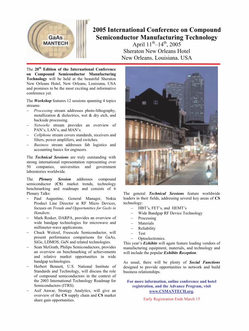
The 20th
Edition of the International Conference
on Compound Semiconductor Manufacturing
Technology will be held at the beautiful Sheraton
New Orleans Hotel, New Orleans, Louisiana, USA
and promises to be the most exciting and informative
conference yet.
The Workshop features 12 sessions spanning 4 topics
streams:
Processing stream addresses photo-lithography,
metallization & dielectrics, wet & dry etch, and
backside processing.
Networks stream provides an overview of
PAN’s, LAN’s, and MAN’s.
Cellphone stream covers standards, receivers and
filters, power amplifiers, and switches.
Business stream addresses fab logistics and
accounting basics for engineers.
The Technical Sessions are truly outstanding with
strong international representation representing over
50 companies, universities and government
laboratories worldwide.
The Plenary Session addresses compound
semiconductor (CS) market trends, technology
benchmarking and roadmaps and consists of 6
Plenary Talks:
Paul Augustine, General Manager, Nokia
Product Line Director at RF Micro Devices,
focuses on Trends and Opportunities for GaAs in Handsets.
Mark Rosker, DARPA, provides an overview of
wide bandgap technologies for microwave and
millimeter-wave applications.
Chuck Weitzel, Freescale Semiconductor, will
present performance comparisons for GaAs,
SiGe, LDMOS, GaN and related technologies.
Sean McGrath, Philips Semiconductors, provides
an overview on benchmarking of achievements
and relative market opportunities in wide
bandgap technologies.
Herbert Bennett, U.S. National Institute of
Standards and Technology, will discuss the role
of compound semiconductors in the context of
the 2003 International Technology Roadmap for
Semiconductors (ITRS).
Asif Anwar, Strategy Analytics, will give an
overview of the CS supply chain and CS market
share gain opportunities.
The general Technical Sessions feature worldwide
leaders in their fields, addressing several key areas of CS
technology:
HBT’s, FET’s, and HEMT’s
Wide Bandgap RF Device Technology
Processing
Materials
Reliability
Test
Optoelectronics.
This year’s Exhibits will again feature leading vendors of
manufacturing equipment, materials, and technology and
will include the popular Exhibits Reception.
As usual, there will be plenty of Social Functions
designed to provide opportunities to network and build
business relationships.
For more information, online conference and hotel
registration, and the Advance Program, visit
www.CSMANTECH.org.
Early Registration Ends March 15
2005 International Conference on Compound
Semiconductor Manufacturing TechnologyApril 11
th–14
th, 2005
Sheraton New Orleans Hotel
New Orleans, Louisiana, USA
COVER STORY compoundsemiconductor.net
COMPOUND SEMICONDUCTOR MARCH 2005 19
The impressive speed and power hand-ling of GaN has been evident for someyears, and the potential of transistors
based on the material is sufficiently promis-ing that the US military and others are fund-ing their development. Now, GaN transistorsaimed at uses in future high-performancemillimeter-wave (MMW) military commu-nications links and X-band radar are beingreported by a number of groups.
The US military employs RF transmittersand receivers for a plethora of applications,which include all-weather radar, surveillance,reconnaissance, electronic attack and com-munications systems. However, power ampli-fiers (PAs) in many systems still use vacuumtubes. As recently as last year, the US Navywas still funding research to improve this tech-nology, in particular for high-data-ratecommunications and high-power, high-fre-quency radar applications.
An ideal PA is small, light, cheap, reliableand efficient, and it should provide high powerdensities, transmit across a wide range ofbandwidths and operate in a broad range oftemperatures. Wide-bandgap semiconductorelectronics can provide power amplification(and low-noise amplification) with the poten-tial advantages of being more compact, robustand longer-lived than vacuum tubes. Beforesolid-state electronics can replace vacuumtubes, however, the technology must be opti-mized and shown to be manufacturable.Material quality and process technology willdictate device performance.
GaAs and silicon PAs are already beingused in some of these military systems, butGaN (along with SiC) can potentially operatefrom VHF through X-band frequencies whileproviding higher breakdown voltage, betterthermal conductivity and wider transmissionbandwidths than conventional devices areable to offer. GaN transistors that are the samesize as GaAs devices can operate at higherpowers with higher impedance.
Within the field of RF applications, MMWcommunications links and X-band radar aretwo major areas of interest. Strategic militarycommunications systems range from 7 to44 GHz and beyond. Some of these will bespace-borne, in which case high efficiency,reliability and low weight are all crucial.Radar traditionally requires very high pulsepowers in the microwave bands from UHF toX-band (8–12 GHz) and beyond, and itincludes a variety of ground, air, ship andmobile platform installations.
Signal quality is paramountMillimeter-wave AlGaN/GaN HEMTs havebeen developed with an emphasis on both out-put signal quality and linearity, and the USNavy is now in the process of testing the life-
times of GaN HEMTs and MMICs.Military systems that use active aperture
antenna arrays need a linear amplifier behindeach antenna element, and GaN is well suitedto provide that amplifier for many of thesecommunications and radar systems. The USNavy has also funded the development ofhigh-power broadband AlGaN HEMT ampli-fiers that emit tens of watts of power at manyfrequencies for use as electronic decoys.
GaN’s competitors can’t keep upOther materials, including GaAs and SiC, can-not measure up to GaN’s ability to providehigh power and high frequency at the sametime. GaN’s wide bandgap of 3.4 eV, highelectron saturation velocity (2.7 × 107 cm/s),low onset resistance and ability to operate athigh temperatures together result in poten-tially high-efficiency devices. GaN can alsooperate at higher voltages: it has a breakdownvoltage of 70 V compared with GaAs’s 5 Vand InP’s 3 V. GaN’s large bandgap alsomakes it much less susceptible to radiationdamage, which provides an additional bene-fit for satellite systems.
Satellite-based communications trans-ceivers need efficient, robust and reliable tran-sistors that can act as power amplifiers atMMW frequencies. Jeong-Sun Moon at HRLLaboratories in Malibu, CA, who presented apaper entitled “Deep-submicron gate-recessedand field-plated AlGaN/GaN HFETs for mil-limeter wave applications” at the MRS Fall2004 meeting in Boston last December,believes that GaN devices compare well toGaAs for Ka-band and even higher-frequencycommunications equipment. “Current GaAspower HEMT technology is hitting a wall try-ing to deliver high power and high efficiencyat the same time,” he said. “GaN may over-come [GaAs] and move beyond it.”
In his talk, Moon said that PAs based onGaAs PHEMTs could produce less than 6 Wof output power in the Ka-band with a power-
Complex US military projects, such as the development of unmanned air-combat systems, demandan investment in high-technology equipment and a likely role for a range of III-V devices. YvonneCarts-Powell describes some recent progress that has been made with GaN transistors.
GAN TRANSISTORS
X-band radar is set to reapbenefits of GaN technology
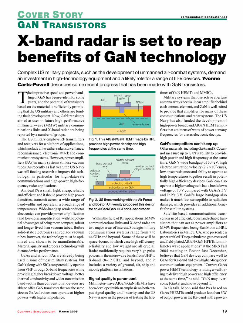
SiNx AlGaN
GaN
4H-SiC
recessed gate
sourcegate
drain
Fig. 1. This AlGaN/GaN HEMT made by HRLprovides high power density and highfrequencies at the same time.
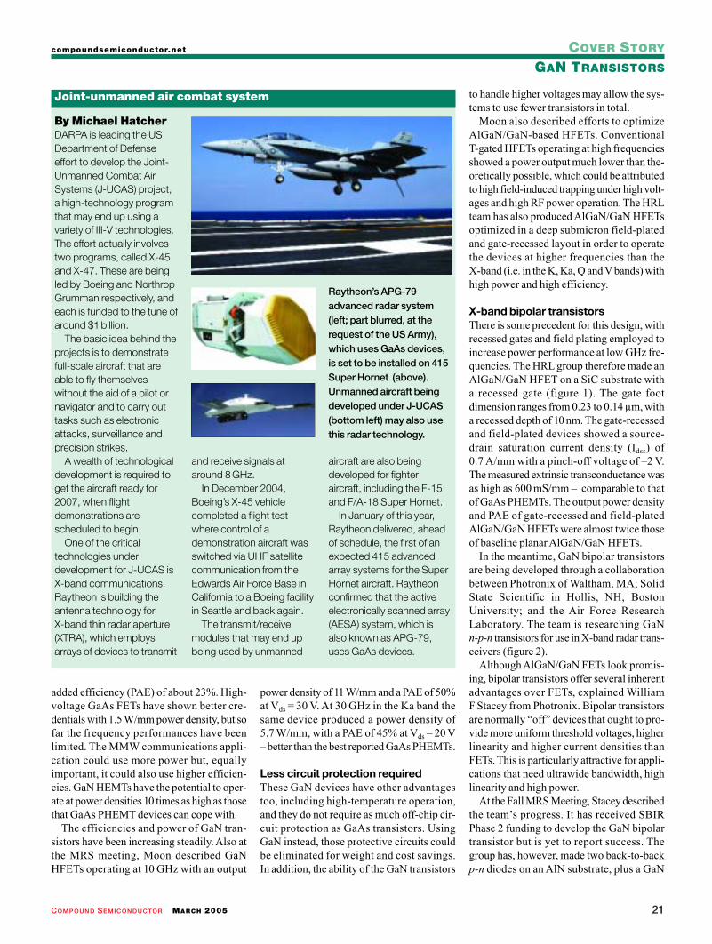
Fig. 2. US firms working with the Air Forceand Boston University proposed this designfor an AlGaN/GaN HBT for X-band radar.
emitter contactmetalbase contact
metal
collectorcontactmetal
emitter contactlayer, n-AlGaN
base, p-GaNcollector, n-GaN
subcollector, n+GaNundoped AlN template

SEMICON® Europa is the industry’s distinctive European forumfor addressing the challenges facing today’s global semiconductorindustry. Thousands of visitors meet at SEMICON Europa eachyear to access:Innovation• An impressive array of new manufacturing tools and solutions from 800 top-notch
industry suppliers exhibiting in more than 33,000 square meters• Technology platforms providing valuable insight through
innovative displays and presentations in MEMS/nanotechnology and photovoltaic
Knowledge• Competitive and market intelligence that allows
you to benchmark the current environment• Specialized technology and business programs
designed to advance your manufacturingknowledge and promote industry best practices
People• Networking opportunities with industry
professionals at all levels of the supply chain• Access to a global network of suppliers in
industry related vertical markets
Register on www.semi.org/semiconeuropafor your FREE exhibit pass today!
For questions, contact:Laura Jäth Melissa GarciaSEMI® Europe SEMI® HeadquartersPh: 32.2.289.6498 Ph: 1.408.943.7009Email: [email protected] Email: [email protected]
Access toInnovation—Knowledge—People
12–14 April | New Munich Trade Fair Centre | Munich, Germany
TechnologyPlatform Includes:• Automation
• MEMS/Nanotechnology• Photovoltaic
• Lithography/Masks• Interconnect/Reliability• Front-end Processing
SEM
ICO
NEuro p a2005
21COMPOUND SEMICONDUCTOR MARCH 2005
COVER STORYcompoundsemiconductor.net
GAN TRANSISTORS
added efficiency (PAE) of about 23%. High-voltage GaAs FETs have shown better cre-dentials with 1.5 W/mm power density, but sofar the frequency performances have beenlimited. The MMW communications appli-cation could use more power but, equallyimportant, it could also use higher efficien-cies. GaN HEMTs have the potential to oper-ate at power densities 10 times as high as thosethat GaAs PHEMT devices can cope with.
The efficiencies and power of GaN tran-sistors have been increasing steadily. Also atthe MRS meeting, Moon described GaNHFETs operating at 10 GHz with an output
power density of 11 W/mm and a PAE of 50%at Vds = 30 V. At 30 GHz in the Ka band thesame device produced a power density of5.7 W/mm, with a PAE of 45% at Vds = 20 V– better than the best reported GaAs PHEMTs.
Less circuit protection requiredThese GaN devices have other advantagestoo, including high-temperature operation,and they do not require as much off-chip cir-cuit protection as GaAs transistors. UsingGaN instead, those protective circuits couldbe eliminated for weight and cost savings.In addition, the ability of the GaN transistors
to handle higher voltages may allow the sys-tems to use fewer transistors in total.
Moon also described efforts to optimizeAlGaN/GaN-based HFETs. ConventionalT-gated HFETs operating at high frequenciesshowed a power output much lower than the-oretically possible, which could be attributedto high field-induced trapping under high volt-ages and high RF power operation. The HRLteam has also produced AlGaN/GaN HFETsoptimized in a deep submicron field-platedand gate-recessed layout in order to operatethe devices at higher frequencies than theX-band (i.e. in the K, Ka, Q and V bands) withhigh power and high efficiency.
X-band bipolar transistorsThere is some precedent for this design, withrecessed gates and field plating employed toincrease power performance at low GHz fre-quencies. The HRL group therefore made anAlGaN/GaN HFET on a SiC substrate witha recessed gate (figure 1). The gate footdimension ranges from 0.23 to 0.14 µm, witha recessed depth of 10 nm. The gate-recessedand field-plated devices showed a source-drain saturation current density (Idss) of0.7 A/mm with a pinch-off voltage of –2 V.The measured extrinsic transconductance wasas high as 600 mS/mm – comparable to thatof GaAs PHEMTs. The output power densityand PAE of gate-recessed and field-platedAlGaN/GaN HFETs were almost twice thoseof baseline planar AlGaN/GaN HFETs.
In the meantime, GaN bipolar transistorsare being developed through a collaborationbetween Photronix of Waltham, MA; SolidState Scientific in Hollis, NH; BostonUniversity; and the Air Force ResearchLaboratory. The team is researching GaNn-p-n transistors for use in X-band radar trans-ceivers (figure 2).
Although AlGaN/GaN FETs look promis-ing, bipolar transistors offer several inherentadvantages over FETs, explained WilliamF Stacey from Photronix. Bipolar transistorsare normally “off” devices that ought to pro-vide more uniform threshold voltages, higherlinearity and higher current densities thanFETs. This is particularly attractive for appli-cations that need ultrawide bandwidth, highlinearity and high power.
At the Fall MRS Meeting, Stacey describedthe team’s progress. It has received SBIRPhase 2 funding to develop the GaN bipolartransistor but is yet to report success. Thegroup has, however, made two back-to-backp-n diodes on an AlN substrate, plus a GaN
By Michael HatcherDARPA is leading the USDepartment of Defenseeffort to develop the Joint-Unmanned Combat AirSystems (J-UCAS) project,a high-technology programthat may end up using avariety of III-V technologies.The effort actually involvestwo programs, called X-45and X-47. These are beingled by Boeing and NorthropGrumman respectively, andeach is funded to the tune ofaround $1 billion.
The basic idea behind theprojects is to demonstratefull-scale aircraft that areable to fly themselveswithout the aid of a pilot ornavigator and to carry outtasks such as electronicattacks, surveillance andprecision strikes.
A wealth of technologicaldevelopment is required toget the aircraft ready for2007, when flightdemonstrations arescheduled to begin.
One of the criticaltechnologies underdevelopment for J-UCAS isX-band communications.Raytheon is building theantenna technology forX-band thin radar aperture(XTRA), which employsarrays of devices to transmit
and receive signals ataround 8 GHz.
In December 2004,Boeing’s X-45 vehiclecompleted a flight testwhere control of ademonstration aircraft wasswitched via UHF satellitecommunication from theEdwards Air Force Base inCalifornia to a Boeing facilityin Seattle and back again.
The transmit/receivemodules that may end upbeing used by unmanned
aircraft are also beingdeveloped for fighteraircraft, including the F-15and F/A-18 Super Hornet.
In January of this year,Raytheon delivered, aheadof schedule, the first of anexpected 415 advancedarray systems for the SuperHornet aircraft. Raytheonconfirmed that the activeelectronically scanned array(AESA) system, which isalso known as APG-79,uses GaAs devices.
Joint-unmanned air combat system
Raytheon’s APG-79advanced radar system(left; part blurred, at therequest of the US Army),which uses GaAs devices,is set to be installed on 415Super Hornet (above).Unmanned aircraft beingdeveloped under J-UCAS(bottom left) may also usethis radar technology.
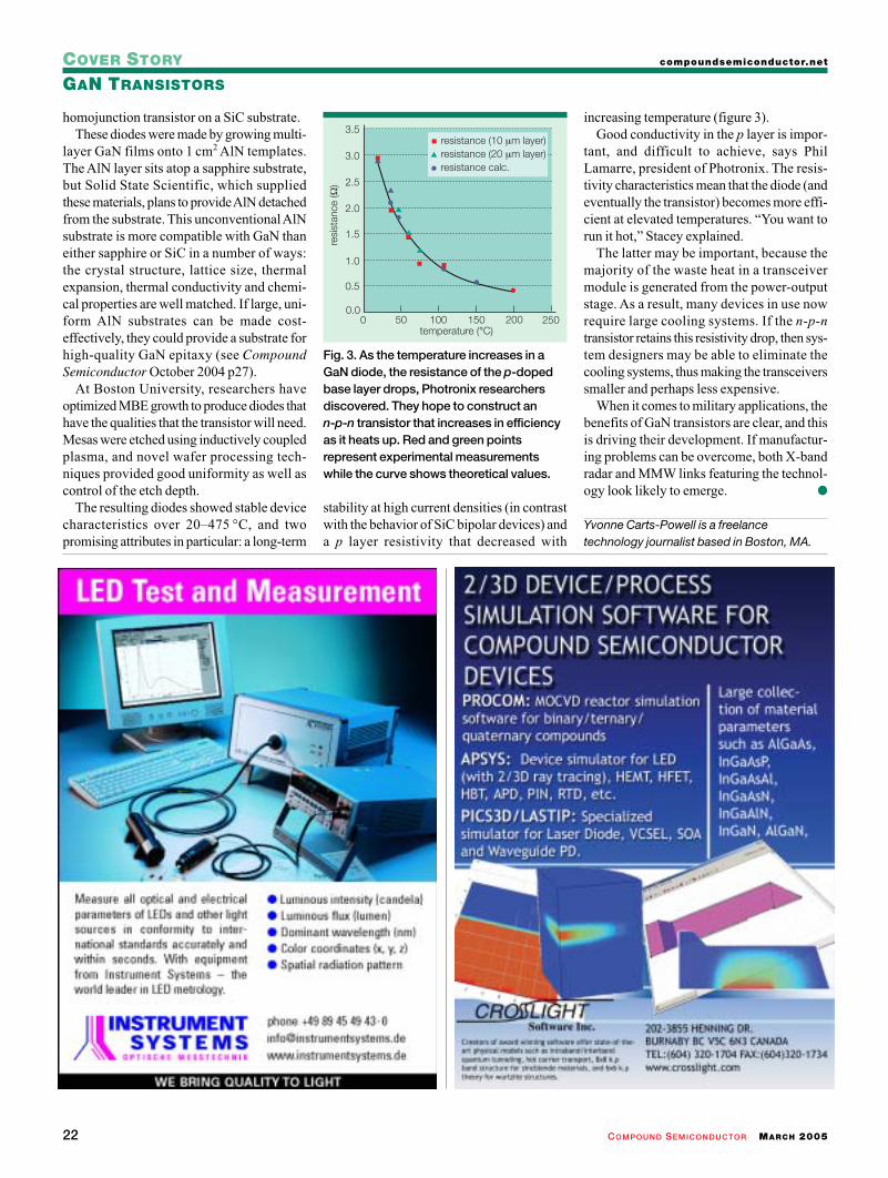
COVER STORY compoundsemiconductor.net
COMPOUND SEMICONDUCTOR MARCH 200522
GAN TRANSISTORS
homojunction transistor on a SiC substrate.These diodes were made by growing multi-
layer GaN films onto 1 cm2 AlN templates.The AlN layer sits atop a sapphire substrate,but Solid State Scientific, which suppliedthese materials, plans to provide AlN detachedfrom the substrate. This unconventional AlNsubstrate is more compatible with GaN thaneither sapphire or SiC in a number of ways:the crystal structure, lattice size, thermalexpansion, thermal conductivity and chemi-cal properties are well matched. If large, uni-form AlN substrates can be made cost-effectively, they could provide a substrate forhigh-quality GaN epitaxy (see CompoundSemiconductor October 2004 p27).
At Boston University, researchers haveoptimized MBE growth to produce diodes thathave the qualities that the transistor will need.Mesas were etched using inductively coupledplasma, and novel wafer processing tech-niques provided good uniformity as well ascontrol of the etch depth.
The resulting diodes showed stable devicecharacteristics over 20–475 °C, and twopromising attributes in particular: a long-term
stability at high current densities (in contrastwith the behavior of SiC bipolar devices) anda p layer resistivity that decreased with
increasing temperature (figure 3).Good conductivity in the p layer is impor-
tant, and difficult to achieve, says PhilLamarre, president of Photronix. The resis-tivity characteristics mean that the diode (andeventually the transistor) becomes more effi-cient at elevated temperatures. “You want torun it hot,” Stacey explained.
The latter may be important, because themajority of the waste heat in a transceivermodule is generated from the power-outputstage. As a result, many devices in use nowrequire large cooling systems. If the n-p-ntransistor retains this resistivity drop, then sys-tem designers may be able to eliminate thecooling systems, thus making the transceiverssmaller and perhaps less expensive.
When it comes to military applications, thebenefits of GaN transistors are clear, and thisis driving their development. If manufactur-ing problems can be overcome, both X-bandradar and MMW links featuring the technol-ogy look likely to emerge.
Yvonne Carts-Powell is a freelancetechnology journalist based in Boston, MA.
0 50 100 150 200 250temperature (°C)
0.0
0.5
1.0
1.5
2.0
2.5
3.0
3.5
resi
stan
ce (Ω
)
resistance (10 µm layer)resistance (20 µm layer)resistance calc.
Fig. 3. As the temperature increases in aGaN diode, the resistance of the p-dopedbase layer drops, Photronix researchersdiscovered. They hope to construct ann-p-n transistor that increases in efficiencyas it heats up. Red and green pointsrepresent experimental measurementswhile the curve shows theoretical values.
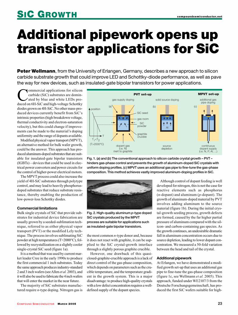
SIC GROWTH compoundsemiconductor.net
COMPOUND SEMICONDUCTOR MARCH 2005 23
Additional pipework opens uptransistor applications for SiC
Commercial applications for siliconcarbide (SiC) substrates are domin-ated by blue and white LEDs pro-
duced on 6H-SiC and high-voltage Schottkydiodes grown on 4H-SiC. No other mass-pro-duced devices currently benefit from SiC’sintrinsic properties (high breakdown voltage,thermal conductivity and electron-saturationvelocity), but this could change if improve-ments can be made to the material’s dopinguniformity and the range of dopants available.
Modified physical vapor transport (MPVT),an alternative method for bulk wafer growth,could be the answer. This approach has pro-duced aluminum-doped substrates that are suit-able for insulated-gate bipolar transistors(IGBTs) – devices that could be used in elec-trical power converters and power circuits forthe control of higher-power electrical motors.
The MPVT process could also increase theyield of 4H-SiC substrates through polytypecontrol, and may lead to heavily phosphorus-doped substrates that reduce substrate resis-tance, thereby enabling the production oflow-power-loss Schottky diodes.
Commercial limitationsBulk single crystals of SiC that provide sub-strates for industrial device fabrication areusually grown by a seeded-sublimation tech-nique, referred to as either physical vaportransport (PVT) or the modified Lely tech-nique. The process involves sublimating SiCpowder at high temperatures (T>2000°C), fol-lowed by recrystallization on a slightly coolersingle-crystal SiC seed (figure 1a).
It is a method that was used by current mar-ket leader Cree in the early 1990s to producethe first commercial 1 inch substrates. Todaythe same approach produces industry-standard2 and 3 inch wafers (see Allen et al. 2003), andit will also be used to fabricate the 4inch wafersthat will enter the market in the near future.
The majority of SiC substrates manufac-tured require n-type doping. Nitrogen gas is
the most common n-type donor and, becauseit does not react with graphite, it can be sup-plied to the SiC crystal-growth interfacethrough a slightly porous graphite crucible.
However, one drawback of this quasi-closed-graphite-crucible approach is a lack ofdirect control of the gas-phase composition,which depends on parameters such as the cru-cible temperature, and the temperature gradi-ent in the growth system. This is a majordisadvantage: to produce high-quality crystalswith a low defect concentration requires a well-defined supply of the dopant species.
Although control of dopant feeding is welldeveloped for nitrogen, this is not the case forreactive elements such as phosphorus(n-dopant) and aluminum (p-dopant). Thegrowth of aluminum-doped material by PVTinvolves adding aluminum to the sourcematerial (figure 1b). During the initial crys-tal-growth seeding process, growth defectsare formed, caused by the far higher partialpressure of aluminum compared with the sil-icon- and carbon-containing gas species. Asthe growth continues, an undesirable dramaticfall in aluminum concentration occurs due tosource depletion, leading to lower dopant con-centration. We measured a 50-fold variationbetween the head and tail of the crystal.
Additional pipeworkAt Erlangen, we have demonstrated a modi-fied growth set-up that uses an additional gaspipe to fine-tune the gas-phase composition(figure 1c, see Wellmann et al. 2005). Thisapproach, funded under WE2107/3 from theDeutsche Forschungsgemeinschaft, has pro-duced the first SiC wafers suitable for high-
Peter Wellmann, from the University of Erlangen, Germany, describes a new approach to siliconcarbide substrate growth that could improve LED and Schottky-diode performance, as well as pavethe way for new devices, such as insulated-gate bipolar transistors for power applications.
position
T1<T2(T>2000°C)
T
dopant gas(i.e. N)
inert to graphite
(a)
SiC seed
gas room
SiCpowder
graphitecrucible
gas supply doping solid source doping
Al
sourcedepletion
continuousdopant supply(i.e. N, P, Al, ...)
additional gaspipe doping
MPVT set-upPVT set-up
(b) (c)
Fig. 1. (a) and (b) The conventional approach to silicon carbide crystal growth – PVT –hinders gas-phase control and prevents the growth of aluminum-doped SiC crystals withuniform doping profiles. (c) MPVT uses an additional gas pipe to fine-tune the gas-phasecomposition. This method achieves vastly improved aluminum-doping profiles in SiC.
Fig. 2. High-quality aluminum p-type dopedSiC crystals produced by the MPVTprocess are suitable for applications suchas insulated-gate bipolar transistors.
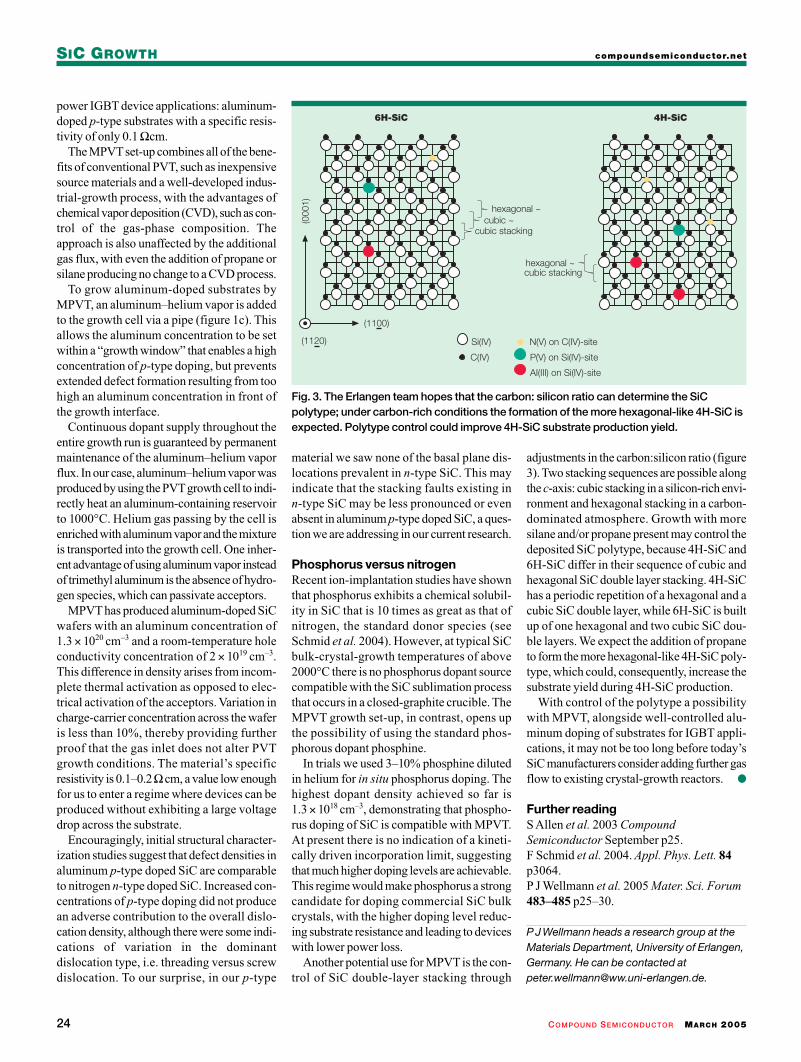
SIC GROWTH compoundsemiconductor.net
COMPOUND SEMICONDUCTOR MARCH 200524
power IGBT device applications: aluminum-doped p-type substrates with a specific resis-tivity of only 0.1 Ωcm.
The MPVTset-up combines all of the bene-fits of conventional PVT, such as inexpensivesource materials and a well-developed indus-trial-growth process, with the advantages ofchemical vapor deposition (CVD), such as con-trol of the gas-phase composition. Theapproach is also unaffected by the additionalgas flux, with even the addition of propane orsilane producing no change to a CVD process.
To grow aluminum-doped substrates byMPVT, an aluminum–helium vapor is addedto the growth cell via a pipe (figure 1c). Thisallows the aluminum concentration to be setwithin a “growth window” that enables a highconcentration of p-type doping, but preventsextended defect formation resulting from toohigh an aluminum concentration in front ofthe growth interface.
Continuous dopant supply throughout theentire growth run is guaranteed by permanentmaintenance of the aluminum–helium vaporflux. In our case, aluminum–helium vapor wasproduced by using the PVTgrowth cell to indi-rectly heat an aluminum-containing reservoirto 1000°C. Helium gas passing by the cell isenriched with aluminum vapor and the mixtureis transported into the growth cell. One inher-ent advantage of using aluminum vapor insteadof trimethyl aluminum is the absence of hydro-gen species, which can passivate acceptors.
MPVT has produced aluminum-doped SiCwafers with an aluminum concentration of1.3 × 1020 cm–3 and a room-temperature holeconductivity concentration of 2 × 1019 cm–3.This difference in density arises from incom-plete thermal activation as opposed to elec-trical activation of the acceptors. Variation incharge-carrier concentration across the waferis less than 10%, thereby providing furtherproof that the gas inlet does not alter PVTgrowth conditions. The material’s specificresistivity is 0.1–0.2Ωcm, a value low enoughfor us to enter a regime where devices can beproduced without exhibiting a large voltagedrop across the substrate.
Encouragingly, initial structural character-ization studies suggest that defect densities inaluminum p-type doped SiC are comparableto nitrogen n-type doped SiC. Increased con-centrations of p-type doping did not producean adverse contribution to the overall dislo-cation density, although there were some indi-cations of variation in the dominantdislocation type, i.e. threading versus screwdislocation. To our surprise, in our p-type
material we saw none of the basal plane dis-locations prevalent in n-type SiC. This mayindicate that the stacking faults existing inn-type SiC may be less pronounced or evenabsent in aluminum p-type doped SiC, a ques-tion we are addressing in our current research.
Phosphorus versus nitrogenRecent ion-implantation studies have shownthat phosphorus exhibits a chemical solubil-ity in SiC that is 10 times as great as that ofnitrogen, the standard donor species (seeSchmid et al. 2004). However, at typical SiCbulk-crystal-growth temperatures of above2000°C there is no phosphorus dopant sourcecompatible with the SiC sublimation processthat occurs in a closed-graphite crucible. TheMPVT growth set-up, in contrast, opens upthe possibility of using the standard phos-phorous dopant phosphine.
In trials we used 3–10% phosphine dilutedin helium for in situ phosphorus doping. Thehighest dopant density achieved so far is1.3 × 1018 cm–3, demonstrating that phospho-rus doping of SiC is compatible with MPVT.At present there is no indication of a kineti-cally driven incorporation limit, suggestingthat much higher doping levels are achievable.This regime would make phosphorus a strongcandidate for doping commercial SiC bulkcrystals, with the higher doping level reduc-ing substrate resistance and leading to deviceswith lower power loss.
Another potential use for MPVT is the con-trol of SiC double-layer stacking through
adjustments in the carbon:silicon ratio (figure3). Two stacking sequences are possible alongthe c-axis: cubic stacking in a silicon-rich envi-ronment and hexagonal stacking in a carbon-dominated atmosphere. Growth with moresilane and/or propane present may control thedeposited SiC polytype, because 4H-SiC and6H-SiC differ in their sequence of cubic andhexagonal SiC double layer stacking. 4H-SiChas a periodic repetition of a hexagonal and acubic SiC double layer, while 6H-SiC is builtup of one hexagonal and two cubic SiC dou-ble layers. We expect the addition of propaneto form the more hexagonal-like 4H-SiC poly-type, which could, consequently, increase thesubstrate yield during 4H-SiC production.
With control of the polytype a possibilitywith MPVT, alongside well-controlled alu-minum doping of substrates for IGBT appli-cations, it may not be too long before today’sSiC manufacturers consider adding further gasflow to existing crystal-growth reactors.
Further readingS Allen et al. 2003 CompoundSemiconductor September p25.F Schmid et al. 2004. Appl. Phys. Lett. 84p3064.P J Wellmann et al. 2005 Mater. Sci. Forum483–485 p25–30.
P J Wellmann heads a research group at theMaterials Department, University of Erlangen,Germany. He can be contacted [email protected].
(000
1)
(1120)
(1100)
hexagonal ~cubic ~
cubic stacking
hexagonal ~cubic stacking
6H-SiC 4H-SiC
Si(IV)
C(IV)
N(V) on C(IV)-site
P(V) on Si(IV)-site
AI(III) on Si(IV)-site
Fig. 3. The Erlangen team hopes that the carbon: silicon ratio can determine the SiCpolytype; under carbon-rich conditions the formation of the more hexagonal-like 4H-SiC isexpected. Polytype control could improve 4H-SiC substrate production yield.
With a cohesive and complete team of professionals, Bandwidth Semiconductor continues to growin today's marketplace. We operate a complete compound semiconductor growth & device fabricationline housed in a 13,500 sq. ft. class 100/1000 cleanroom.
BANDWIDTH SEMICONDUCTOR, LLC25 Sagamore Park Rd., Hudson, NH 03051
www.bandwidthsemi.com(603) 595-8900
Epitaxial and Foundry Inquiries: [email protected] M/F/D/V
Epitaxial Services MOCVD Experts – 20 Years ExperienceOur extensive MOCVD experience and capacity enable us to grow a wide range ofGaAs and InP epitaxial structures to our ownor to customer's designs.
• GaAs and InP-based materials• 2", 3", 4" Custom Epi-Wafer Capability• Excellent Uniformity & Reproducibility• Production & Development Quantities
Foundry ServicesWe design the process steps and conditions tomeet the desired device characteristics andimplement the process in our fab. Processequipment includes:
• PECVD • Metallization • Wet & Dry Etch• Photolithography • Dielectric & Optical Thin Film Deposition• Wafer Polishing, Lapping, Dicing & Cleaving
European Sole Agent of
• Arsenic 7N5 MBE slugs• Arsenic 6N, 7N, 7N5 chunks
Tel : 0033-1-44 73 10 70 Fax : 0033-1-44 73 10 [email protected]
Your MBE materialsone stop shop
• Arsenic 7N5• Gallium 7N• Indium 7N• Aluminium 6N5• Red Phosphorous 7N• Magnesium 6N• Manganese 5N8• Antimony 7N• Beryllium 5N• Silicon Dopant• PBN Crucibles
Your Wafersone stop shop
• Indium Antimonide• Indium Arsenide• Indium Phosphide• Gallium Antimonide• Gallium Arsenide• Gallium Phosphide• Silicon Carbide• Silicon • Sapphire
NewTMGa, TM In, DE Zn, Ce, Dy, Er, Gd, HfO2,Ho, La, Lu, Nd, Pr, Sm, Sc, Ta, Tb, Tm, Yb, Y
WWW.ARNAUDELECTRONICS.COM
COMPOUND SEMICONDUCTOR MARCH 200526
SUPPLIERS GUIDECHARACTERIZATION, TEST & MEASUREMENTIf you would like to advertise in future issues, contact Luke Neel (tel: +44 117 930 1033, fax: +44 117 920 0809, e-mail: [email protected]).
Char
acte
rizat
ion,
Tes
t & M
easu
rem
ent S
uppl
iers
Gui
de
Com
pany
nam
eW
eb a
ddre
ssTe
leph
one
num
ber
Cont
act
CL equipmemt
CV, hall equipment
Electron microscope, AFM and spectroscopy equipment
Materials characterization equipment
Other wafer characterization equipment
PL Raman equipment
SIMS equipment
X-ray diffraction equipment
Defect inspection
Laser beam profiling
LED output measurement
RF probe stations, cards and test equipment
Wafer-level burn-in and test equipment
Other test and measurement products
Acce
l-RF
acce
lrf.c
om+1
858
449
975
0Ro
land
Sha
w
Acce
nt O
ptic
alTe
chno
logi
esac
cent
opto
.com
+44
1904
715
500
Dal
e Pa
ge
KLA-
Tenc
ore
kla-
tenc
ore.
com
+1 5
10 4
56 2
490
Fran
k Bu
rkee
n
Inst
rum
ent
Syst
ems
inst
rum
ents
yste
ms.
com
+49
89 4
5494
3 24
Pete
r Läp
ple
Lake
Sho
reCr
yotro
nics
Inc
lake
shor
e.co
m+1
614
891
224
4Sa
les
Dep
artm
ent
Mic
rom
anip
ulat
orm
icro
man
ipul
ator
.com
+1 7
75 8
82 2
400
Mel
issa
Wic
kste
ad
Opt
roni
cLa
bora
torie
sol
inet
.com
+1 4
07 4
42 3
171
Mau
reen
Kno
wle
s
ORS
Ltd
ww
w.o
rs-lt
d.co
m+4
4 17
45 5
35 1
88Ke
lvin
Wee
ks
Suss
Mic
roTe
cw
ww
.sus
s.co
m+4
9 35
240
730
Mic
hael
Har
z
SUPPLIERS GUIDE SPONSORS
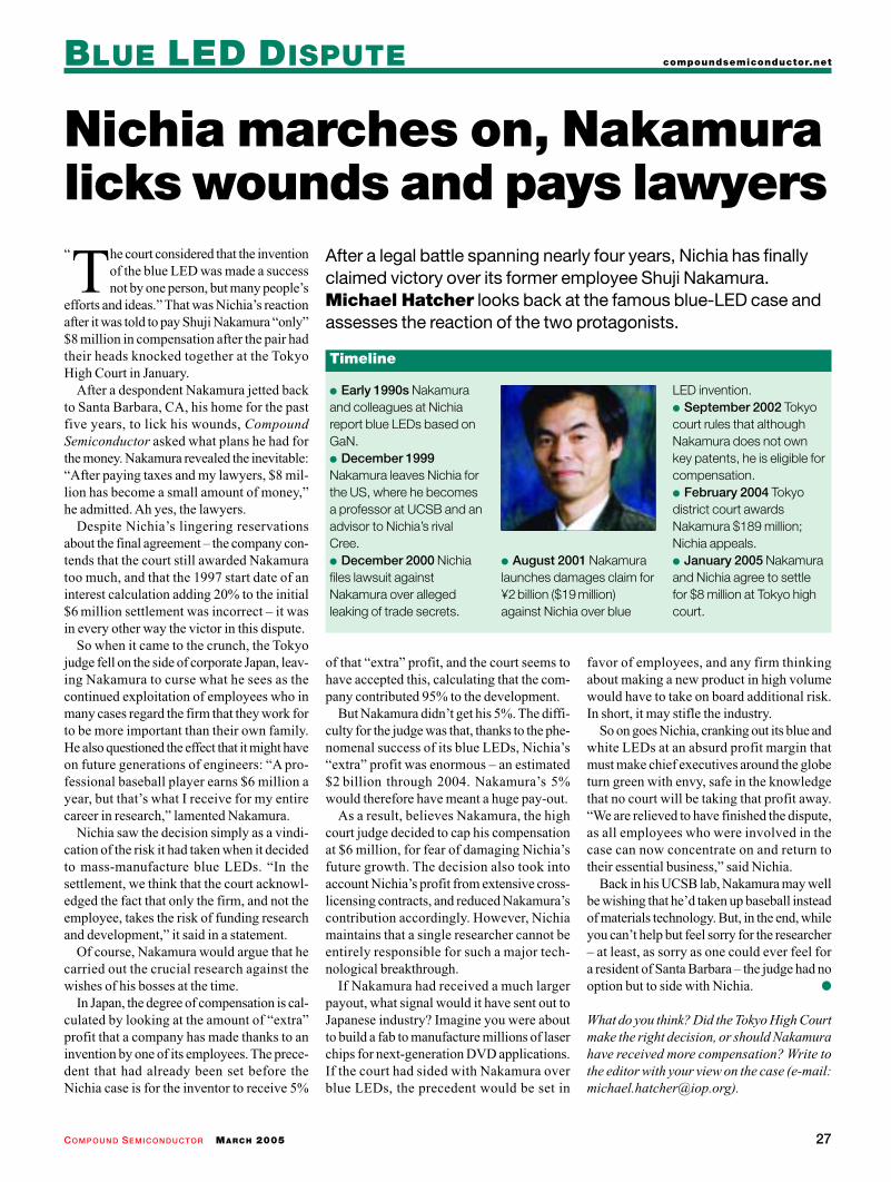
BLUE LED DISPUTE compoundsemiconductor.net
COMPOUND SEMICONDUCTOR MARCH 2005 27
Nichia marches on, Nakamuralicks wounds and pays lawyers
The court considered that the inventionof the blue LED was made a successnot by one person, but many people’s
efforts and ideas.” That was Nichia’s reactionafter it was told to pay Shuji Nakamura “only”$8 million in compensation after the pair hadtheir heads knocked together at the TokyoHigh Court in January.
After a despondent Nakamura jetted backto Santa Barbara, CA, his home for the pastfive years, to lick his wounds, CompoundSemiconductor asked what plans he had forthe money. Nakamura revealed the inevitable:“After paying taxes and my lawyers, $8 mil-lion has become a small amount of money,”he admitted. Ah yes, the lawyers.
Despite Nichia’s lingering reservationsabout the final agreement – the company con-tends that the court still awarded Nakamuratoo much, and that the 1997 start date of aninterest calculation adding 20% to the initial$6 million settlement was incorrect – it wasin every other way the victor in this dispute.
So when it came to the crunch, the Tokyojudge fell on the side of corporate Japan, leav-ing Nakamura to curse what he sees as thecontinued exploitation of employees who inmany cases regard the firm that they work forto be more important than their own family.He also questioned the effect that it might haveon future generations of engineers: “A pro-fessional baseball player earns $6 million ayear, but that’s what I receive for my entirecareer in research,” lamented Nakamura.
Nichia saw the decision simply as a vindi-cation of the risk it had taken when it decidedto mass-manufacture blue LEDs. “In thesettlement, we think that the court acknowl-edged the fact that only the firm, and not theemployee, takes the risk of funding researchand development,” it said in a statement.
Of course, Nakamura would argue that hecarried out the crucial research against thewishes of his bosses at the time.
In Japan, the degree of compensation is cal-culated by looking at the amount of “extra”profit that a company has made thanks to aninvention by one of its employees. The prece-dent that had already been set before theNichia case is for the inventor to receive 5%
of that “extra” profit, and the court seems tohave accepted this, calculating that the com-pany contributed 95% to the development.
But Nakamura didn’t get his 5%. The diffi-culty for the judge was that, thanks to the phe-nomenal success of its blue LEDs, Nichia’s“extra” profit was enormous – an estimated$2 billion through 2004. Nakamura’s 5%would therefore have meant a huge pay-out.
As a result, believes Nakamura, the highcourt judge decided to cap his compensationat $6 million, for fear of damaging Nichia’sfuture growth. The decision also took intoaccount Nichia’s profit from extensive cross-licensing contracts, and reduced Nakamura’scontribution accordingly. However, Nichiamaintains that a single researcher cannot beentirely responsible for such a major tech-nological breakthrough.
If Nakamura had received a much largerpayout, what signal would it have sent out toJapanese industry? Imagine you were aboutto build a fab to manufacture millions of laserchips for next-generation DVD applications.If the court had sided with Nakamura overblue LEDs, the precedent would be set in
favor of employees, and any firm thinkingabout making a new product in high volumewould have to take on board additional risk.In short, it may stifle the industry.
So on goes Nichia, cranking out its blue andwhite LEDs at an absurd profit margin thatmust make chief executives around the globeturn green with envy, safe in the knowledgethat no court will be taking that profit away.“We are relieved to have finished the dispute,as all employees who were involved in thecase can now concentrate on and return totheir essential business,” said Nichia.
Back in his UCSB lab, Nakamura may wellbe wishing that he’d taken up baseball insteadof materials technology. But, in the end, whileyou can’t help but feel sorry for the researcher– at least, as sorry as one could ever feel fora resident of Santa Barbara – the judge had nooption but to side with Nichia.
What do you think? Did the Tokyo High Courtmake the right decision, or should Nakamurahave received more compensation? Write tothe editor with your view on the case (e-mail:[email protected]).
After a legal battle spanning nearly four years, Nichia has finallyclaimed victory over its former employee Shuji Nakamura.Michael Hatcher looks back at the famous blue-LED case andassesses the reaction of the two protagonists.
Early 1990s Nakamuraand colleagues at Nichiareport blue LEDs based onGaN. December 1999Nakamura leaves Nichia forthe US, where he becomesa professor at UCSB and anadvisor to Nichia’s rivalCree. December 2000 Nichiafiles lawsuit againstNakamura over allegedleaking of trade secrets.
August 2001 Nakamuralaunches damages claim for¥2 billion ($19 million)against Nichia over blue
LED invention. September 2002 Tokyocourt rules that althoughNakamura does not ownkey patents, he is eligible forcompensation. February 2004 Tokyodistrict court awardsNakamura $189 million;Nichia appeals. January 2005 Nakamuraand Nichia agree to settlefor $8 million at Tokyo highcourt.
Timeline
“
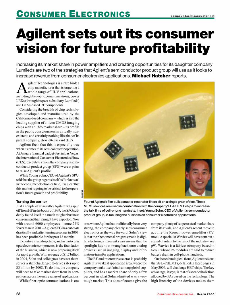
compoundsemiconductor.net
COMPOUND SEMICONDUCTOR MARCH 200528
CONSUMER ELECTRONICS
Agilent sets out its consumervision for future profitability
Agilent Technologies is a rare bird: achip manufacturer that is targeting awhole range of III-V applications,
including fiber-optic communications, powerLEDs (through its part-subsidiary Lumileds)and GaAs-based RF components.
Considering the breadth of chip technolo-gies developed and manufactured by theCalifornia-based company – which is also theleading supplier of silicon CMOS imagingchips with an 18% market share – its profilein the public consciousness is virtually non-existent, and certainly nothing like that of itsparent company, Hewlett-Packard (HP).
Agilent feels that this is especially truewhen it comes to its semiconductor operation.At January’s annual gadget-fest in Las Vegas,the International Consumer Electronics Show(CES), executives from the company’s semi-conductor product group (SPG) were at painsto raise Agilent’s profile.
While Young Sohn, CEO of Agilent’s SPG,said that the group regards itself as “unknown”in the consumer electronics field, it is clear thatthis market is going to be critical to the opera-tion’s future growth and profitability.
Turning the cornerJust a couple of years after Agilent was spunoff from HPin the boom of 1999, the SPG sud-denly found itself in a much tougher businessenvironment than it might have expected. Nowwith around 6000 employees – some 24%fewer than in 2001 – Agilent SPG has cut costsdrastically and, after turning a corner in 2003,has been profitable for the past 18 months.
Expertise in analog chips, and in particularoptoelectronic components, is the foundationof the business, which is now preparing itselffor rapid growth. With revenue of $1.7 billionin 2004, Sohn and colleagues have set them-selves a stiff challenge: to drive sales up to$3 billion by 2008. To do this, the companywill need to take market share from its com-petitors across the entire range of applications.
While fiber-optic communications is one
area where Agilent has traditionally been verystrong, the company clearly sees consumerelectronics as the way forward. Sohn’s viewis that the phenomenal progress made in digi-tal electronics in recent years means that thespotlight has now swung back onto analogdevices used in imaging, display and infor-mation-transfer applications.
The RF and microwave sector is probablyAgilent’s weakest application area, where thecompany ranks itself ninth among global sup-pliers, and has a market share of only a fewpercent in what Sohn admitted was a verytough market. This does of course give the
company plenty of scope to steal market sharefrom its rivals, and Agilent’s recent move toacquire the Korean power-amplifier (PA)module specialist Wavics will have sent out asignal of intent to the rest of the industry (seep9). Wavics is a fabless company based inSeoul whose PA modules are said to reducebattery drain in cell-phone handsets.
On the technological front, Agilent reckonsthat its E-PHEMTs, detailed in these pages inMay 2004, will challenge HBT chips. The keyadvantage, it says, is that of extended talk timeallowed by PAs based on the technology. Thehigh linearity of the devices makes them
Increasing its market share in power amplifiers and creating opportunities for its daughter companyLumileds are two of the strategies that Agilent’s semiconductor product group will use as it looks toincrease revenue from consumer electronics applications. Michael Hatcher reports.
Four of Agilent’s film bulk acoustic-resonator filters sit on a single grain of rice. TheseMEMS devices are used in combination with the company’s E-PHEMT chips to increasethe talk time of cell-phone handsets. Inset: Young Sohn, CEO of Agilent’s semiconductorproduct group, is focusing the business on consumer electronics applications.
AG
ILE
NT
29COMPOUND SEMICONDUCTOR MARCH 2005
CONSUMER ELECTRONICScompoundsemiconductor.net
particularly good for the more complex front-end electronics used in more advanced cellphones. E-PHEMTs are manufactured atAgilent’s 6 inch GaAs fab in Fort Collins, CO,and the company has recently releasedE-PHEMTFETs for base-station applications.
But with its dominant position in CMOSimagers, the camera cell phone is Agilent’score strength, and now its daughter company,Lumileds, is looking to exploit this leadershipas the camera’s performance improves. That’sbecause the more pixels there are in an imag-ing chip, the more light is required to generatesufficient illumination for taking high-qual-ity photos. Xenon lamps currently provide theflash function in such phones, howeverLumileds has worked hard on improving thebrightness of its white LEDs.
Having developed the chip design to sup-port a junction current of around 1A, Lumiledsbelieves that it is well on the way to making itsLEDs competitive with xenon lamps. Andbecause imaging and illumination technologygo hand-in-hand, Lumileds has a straightfor-ward route into the market through Agilent’sexisting leadership position in handsets.
Camera flash was one of many power-LEDmarkets identified by Mike Holt, CEO ofLumileds, during Agilent’s vision summit atthe CES. He also pointed to automotive appli-cations as a large existing market for redpower LEDs in products such as high-mountstop lights. Despite the 50 million new carssold every year, however, Holt said that thissector had “kind of plateaued”, with the rel-atively high cost of the technology still prov-ing to be a barrier for introduction in vehiclesthat are made in very high volumes.
Lumileds now has a partnership with itsother parent company – Philips – that isfocused on developing more LED-based light-ing systems for automotive use.
Rebirth of TrinitronHolt identified two key consumer applicationsin Las Vegas: illuminators for personal hand-held projectors; and backlights for large LCDtelevisions. 450 Luxeon emitters provide thebacklight for Sony’s top-of-the-rage Qualiatelevisions, and Holt did his best to wow theCES delegates with the dazzling color repro-duction that the technology provides. He said
that Sony believes that the technology will bethe “rebirth of Trinitron”.
Trinitron is the advanced cathode-ray-tubetechnology developed at Sony that led to thecompany’s dominance of the television mar-ket in the 1980s. The latest high-spec LCDtelevisions featuring the three-color LEDbacklights are only available in Japan at pre-sent, but Holt hinted that Sony might releasethe televisions in the US shortly.
While many of the applications it is focusedon lie in the future, Lumileds is already enjoy-ing rude financial health. According to Philips,the joint venture made a profit of $62 millionfrom total sales of $280 million in fiscal 2004.That represents a 43% year-on-year growth –in line with the expansion of the overall high-brightness LED market.
Meanwhile, Agilent Labs – the R&D facil-ity that is charged with coming up with theSPG’s next-generation products – has someinnovative ideas in the pipeline. These includean LED-based eyeball-tracking system that isdesigned to monitor and warn drowsy drivers,and a range of fiber-optic systems, includinga prototype 500 Gbit/s optical “engine”.
compoundsemiconductor.netMATERIALS & EQUIPMENT NEWS
COMPOUND SEMICONDUCTOR MARCH 200530
Kopin has received two US patents coveringadvanced wafer technology for next-gener-ation cell-phone power amplifiers (PAs).
Patents 6,847,060 and 6,750,480 cover so-called GAIN-HBT technology, which is basedon the quarternary material system GaAsInN.
According to the Taunton, MA, wafer sup-plier, the physics of the material will enablegreater flexibility in transistor design, some-thing that will become crucial as PAs used incell phones are increasingly required to run athigher frequencies and duty cycles.
Applications such as mobile video will putcurrent PA technology under pressure as datarates increase, and Kopin believes that its tech-nology could be implemented without the usualdifficulties associated with a new material.
“The changes in transistor structure can berendered transparent to the circuit-fabricationprocess, lowering the technological barriersfor implementation,” said Roger Welser,
Kopin’s director of GaAs HBT technology.Welser led the Kopin team that engineered
the GAIN-HBT structure by introducingindium and nitrogen into the 50 nm base layerof a GaAs wafer. The more complex materialincreases the transistor’s frequency range andimproves its temperature stability, whilesimultaneously reducing operating voltage.
Patent 6,750,480 covers basic GAIN-HBTdevice technology, while 6,847,060 describesan enhanced transistor that contains gradedcompositions of the four constituent elements.
“GAIN-HBT transistor wafers provideimprovements in all key areas of mobile appli-ances: performance, battery life, integrationand durability,” said Kopin’s CEO John Fan.
“Although the base layer is only 200 atomiclayers thick and composed of four elementsin varying compositions, production controlallows reproducible growth of these transis-tors for maximum performance advantages.”
Millimetre-wave MMICs offer serious growth potential for device and module manufacturers. CommercialApplications for Millimetre-Wave MMICs, a new strategic report from IOP Publishing, will provide you withcrucial information on the new markets opening up for millimetre-wave technology.
The next big challenge will be to deliver packaged and tested parts that meet the performance, cost andsize criteria being demanded by commercial end-users.
This report will provide you with an insight into the time and resources required for MMIC design andevaluate the emerging technologies being investigated by designers and manufacturers, at both thedevice and subsystem levels, to deliver millimetre-wave solutions to the commercial marketplace.
Give your company the competitive edge …. place an advance order todayTo see an executive summary and table of contents, contact Susan Curtis at [email protected] +44 (0)117 930 1035.
TechnologytrackingNEW REPORT
Order the report before 31 May 2005 and get a FREE copy of the CS-MAX 2004
conference proceedings
Commercial Applications for Millimetre-Wave MMICs
FREE CS-MAX 2004 CONFERENCE PROCEEDINGS WITH YOUR ORDER OF:
OVER 150 PAGES
OF ANALYSIS AND
COMMENTARY
Kopin wins two patents coveringGaAsInN HBT wafer technology UK-based epiwafer supplier IQE says that,
despite a near-term drop in revenue, its orderbook is now at its highest level for two years.
Wireless applications are showingstrongest, with the company having alreadybegun volume shipments to a US-based RF-component maker that decided to close downits own wafer-manufacturing facility.
With more business from Asian customersand US government contractors too, IQE saysthat its wireless unit will be profitable by theend of its fiscal first half, June 30.
In optoelectronics the picture is mixed, withsome weakness in optical-storage applicationsand a flat HB-LED market offset by improv-ing business in telecom and industrial laserapplications.
Overall, the firm expects to report 2004revenue of at least £15.3 million ($28.9 mil-lion). That is slightly down on the 2003 fig-ure, when IQE’s revenue came in at£18.8 million. The company says that a weakthird quarter and a weak US dollar have com-bined to produce the drop.
IQE order book grows
31COMPOUND SEMICONDUCTOR MARCH 2005
MATERIALS & EQUIPMENT NEWScompoundsemiconductor.net
Substrate supplier AXT says that customersare starting to order its 4 inch GaAs substratesnow that it has managed to iron out problemswith material quality.
The Fremont-based company made theannouncement as it attempted to draw a lineunder what has been a tumultuous fiscal 2004in its full-year financial results. After a year inwhich it faced a shareholder lawsuit; took asales hit due to non-compliance with product-testing procedures that led to a boardroomreshuffle; paid a $1.4million charge followinglitigation by rival substrate supplier SumitomoElectric Industries; and laid off 50 employees,AXT reported a net loss of $13.6 million.
That bottom-line figure contrasts with a netloss of $26.7 million in the previous year. At$35.5 million, overall revenue came in justslightly up on 2003 sales.
“We made significant quality improve-ments in our 4 and 6 inch GaAs substrates,”said interim CEO Don Tatzin. “Samples of4 inch-diameter substrates sent to several cus-tomers that were processed using our newcleaning equipment appear to be largely haze-free, similar to our 2 and 3 inch substrates.”
Tatzin adds that the company has recentlywon a number of orders for 4 inch productsfrom customers who had steered clear of AXTfor several months: “We believe that this indi-
cates a turnaround is at hand if we can main-tain high quality.”
In its most recent quarter, however, sales toLED-manufacturing customers declined inwhat AXT called a seasonal fluctuation,although the decline was partially offset byincreased sales of gallium. AXT made a netloss of $2.3million on revenue of $7.6millionin the three months up to December 31, 2004.
Despite the improving picture regardingsubstrate orders, the company forecast rev-enue in the current quarter to be flat, resultingin a net loss of around $3.2million. AXT plansto expand its joint-venture activity in Chinain a bid to return to profitability in 2005.
PRODUCT SHOWCASETo advertise your product in this section, contact Luke Neel on tel: +44 117 930 1033, or e-mail: [email protected].
High-precision scribe dicingMicro Processing Technology
MPT’s new High-Precision Scribe Dicing System for scribingcompound semiconductors and MEMS devices incorporates aporous ceramic vacuum chuck and a scribe force feedback controlsystem to produce scribe lines that are uniform in depth across the
entire surface of the wafer. For the firsttime, this allows the process engineerto optimize and reproduce scribeprocesses to maximize dicing yield andto minimize chip-out.
Contact: Patricia MendellTel: +1 925 299 8940Fax: +1 925 299 8942E-mail: [email protected]: www.microptech.com
Gallium sales help AXT cut loss by half
Magneto-transport measurementsLake Shore Cryotronics, Inc
Hall effect measurements on dilute magnetic semiconductors andcompound semiconductors. Resistance ranges from 10 µΩ to 200 GΩ,fields to 9 T, and temperatures from 2 K to 800 K. Quantitative MobilitySpectrum Analysis software resolves individual carrier mobilities anddensities for multi-carrier devices and compound semiconductors.Anomalous Hall Effect measurements for spintronics and an ACcurrent option measures resistance down to 10 µΩ, and increases
resolution to 10 ppm at 2 mΩ.
Contact: Lake Shore CryotronicsTel: +1 614 891 2244E-mail: [email protected]: www.lakeshore.com
Despite posting a year-on-year fall inrevenue of 22% in 2004, Riber starts 2005with an order backlog worth 79.9 million($12.9 million), almost double the75 million on the books at the beginning ofthe previous year.
The French supplier of MBE equipmentrecorded 713.5 million sales for fiscal2004, comprising three productionmachines netting 73.8 million, 10 researchmachines contributing 75.9 million, andaccessories and spare parts adding
73.7 million. Year-on-year sales increasedby 14% in Europe, but fell by 62% in Asiaand 16% in North America. Oxford Instruments PlasmaTechnology has made the first sale of itsnew Clusterlab600 MBE system to theNational Changhua University ofEducation (NCUE), Taiwan. NCUE willuse the Clusterlab600 tool to grow GaNfilms and epitaxial layers for laser diodes,including DVD lasers and VCSELs, as wellas for InGaN- and AlGaN-based LED
devices. Other intended applicationsinclude spintronics, with the growth ofepitaxial Mn-doped GaN/InGaN films. Lasertel has purchased a GEN200 MBEsystem from Veeco Instruments to increaseits capacity for the production of high-power laser diodes. The Tucson, AZ,company, which uses solid-source MBEtechnology to produce its lasers, says that itselected the GEN200 MBE system in partfor its silicon-style, cluster-tool wafer-handling feature.
In brief
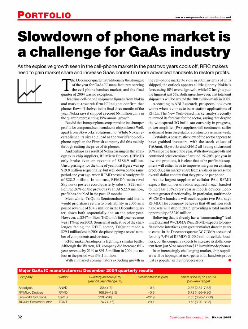
www.compoundsemiconductor.netPORTFOLIO
COMPOUND SEMICONDUCTOR MARCH 200532
The December quarter is traditionally the strongestof the year for GaAs IC manufacturers servingthe cell-phone handset market, and the final
quarter of 2004 was no exception.Headline cell-phone shipment figures from Nokia
and market-research firm IC Insights confirm thatphones flew off shelves in the final three months of theyear. Nokia says it shipped a record 66 million units inthe quarter, representing 19% annual growth.
But did that bumper phone crop translate into bumperprofits for compound semiconductor chipmakers? Well,apart from Skyworks Solutions, no. While Nokia re-established its sizeable lead as the world’s top cell-phone supplier, the Finnish company did this mainlythrough cutting the price of its phones.
And perhaps as a result of Nokia passing on that strat-egy to its chip suppliers, RF Micro Devices (RFMD)only broke even on revenue of $186.9 million.Unsurprisingly for the time of year, that figure was up$19.8 million sequentially, but well down on the sameperiod one year ago, when RFMD posted a handy profitof $28.2 million. In contrast, RFMD’s main rivalSkyworks posted record quarterly sales of $220 mil-lion, up 26% on the previous year. At $22.9 million,profit has doubled in the past 12 months.
Meanwhile, TriQuint Semiconductor said that itwould prioritize a return to profitability in 2005 as itposted revenue of $74.7 million in the December quar-ter, down both sequentially and on the prior year.However, at $347 million, TriQuint’s full-year revenuewas 11% up on 2003. Somewhat indicative of the chal-lenges facing the RFIC sector, TriQuint made a$29.1million loss in 2004 despite shipping a record num-ber of components and devices.
RFIC maker Anadigics is fighting a similar battle.Although the Warren, NJ, company did increase full-year revenue by 21% to $91.3 million in 2004, its netloss in the period was $43.1 million.
With all market commentators expecting growth in
the cell-phone market to slow in 2005, in terms of unitsshipped, the outlook appears a little gloomy. Nokia isforecasting 10% overall growth, while IC Insights putsthe figure at just 5%. Both agree, however, that total unitshipments will be around the 700 million mark in 2005.
According to ABI Research, prospects look evenworse when it comes to base-station applications ofRFICs. The New York-based market analyst recentlyreiterated its forecast for the sector, saying that despitethe widespread 3G build-out currently in progress,power-amplifier (PA) suppliers will continue to sufferas demand from base-station constructors remains weak.
Certainly, a pessimistic view of the sector appears tohave grabbed investors, with the stock values ofTriQuint, Skyworks and RFMD all having slid around20% since the turn of the year. With slowing growth andcontinued price erosion of around 15–20% per year inlow-end products, it is clear that to be profitable sup-pliers will either have to improve margins on existingproducts, gain market share from rivals, or increase theoverall dollar content that they provide per phone.
As the largest supplier of cellular PAs, RFMDexpects the number of radios required in each handsetto increase 30% every year as mobile devices incor-porate greater functionality. In particular, multimodeW-CMDA handsets will each require two PAs, saysRFMD. The company believes that 40 million suchhandsets will ship in 2005, providing a total marketopportunity of $240 million.
Believing that it already has a “commanding” leadin EDGE and W-CDMAPAs, RFMD expects to bene-fit as these interfaces gain greater market share in yearsto come. In the December quarter, W-CDMAaccountedfor only 7.4% of RFMD’s $150.5 million cellular busi-ness, but the company expects to increase its dollar con-tent from just $2 to more than $12 in multimode phones.
In an increasingly challenging market, chip suppli-ers will be hoping that next-generation handsets provejust as popular as their predecessors.
Slowdown of phone market isa challenge for GaAs industry
Anadigics ANAD 22.4 (–5) –10.3 2.56 (2.34–7.68)RF Micro Devices RFMD 168.9 (–12.5) +0.6 5.72 (4.66–9.80)Skyworks Solutions SWKS 220 (+26) +22.9 7.55 (6.98–12.68)TriQuint Semiconductor TQNT 74.7 (–16) –29.1 3.58 (3.20–8.95)
Company Symbol Quarterly revenue ($ m) Net income/loss ($ m) Share price ($) on Feb 14(year on year change, %) (52-week range)
Major GaAs IC manufacturers: December 2004 quarterly results
As the explosive growth seen in the cell-phone market in the past two years cools off, RFIC makersneed to gain market share and increase GaAs content in more advanced handsets to restore profits.

Solutions for a nanoscale world.
For high-volume production of compound semiconductors from GaN LEDs to RF integrated circuits, Veeco provides the world's leading epitaxial equipment and processsolutions. Higher throughput, performance and quality give you a clear advantage.Coupled with our worldwide customer service, and complementary deposition, etch and metrology solutions, these tools make Veeco your ideal production partner. To learn more, visit www.veeco.com or call 1.888.24.VEECO today.
For high-volume epitaxial production, there’s only one choice: Veeco.
Veeco MOCVD and MBE: highest throughput, lowest cost of ownership, superior quality.
Compound SemiconductorSolutions:
MBE, MOCVD, PVD, IBD, IBEAFM and Optical MetrologyProcess Integration Center
Veeco’s high-volume GaNzilla™ MOCVD system.