Embed Size (px)
Citation preview
Contents
DC Biasing of BJTs
DC Biasing of BJTs
Three States of Operation
BJT DC Analysis
DC Biasing CircuitsFixed-Bias Circuit
Emitter-Stabilized Bias Circuit
Voltage Divider Bias Circuit
DC Bias with Voltage Feedback
Various Dierent Bias Circuits
pnp Transistors
Bias StabilizationStability Factors
Stability of Transistor Circuits with Active Components
Practical ApplicationsRelay Driver
Transistor Switch
Transistor Switching Networks
Logic Gates
Current Mirror
Voltage Level Indicator
Dr. U. Sezen & Dr. D. Gökçen (Hacettepe Uni.) ELE230 Electronics I 15-Mar-2017 1 / 59
DC Biasing of BJTs DC Biasing of BJTs
DC BiasingBiasing refers to the DC voltages applied to the transistor to put it into active mode, sothat it can amplify the AC signal.
The DC input establishes an operating point or quiescent point called the Q-point.
Proper DC biasing should try to set the Q-point towards the middle of active region, e.g.,Point B in the gure below.
Dr. U. Sezen & Dr. D. Gökçen (Hacettepe Uni.) ELE230 Electronics I 15-Mar-2017 2 / 59
DC Biasing of BJTs Three States of Operation
Three States of Operation
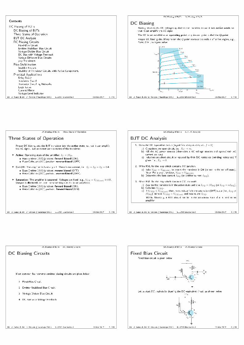
Proper DC biasing sets the BJT transistor into the active state, so that it can amplifythe AC signal. Let us remember the states of the transistor:
I Active: Operating state of the amplier: IC = βIB .
Base-Emitter (BE) junction: forward-biased (ON).Base-Collector (BC) junction: reverse-biased (OFF).
I Cut-O: The amplier is basically o. There is no current, i.e., IC = IB = IE = 0A.
Base-Emitter (BE) junction: reverse-biased (OFF).Base-Collector (BC) junction: reverse-biased (OFF).
I Saturation: The amplier is saturated. Voltages are xed, e.g., VCE = VCE(sat)∼= 0V.
Output is distorted, i.e., not the same shape as the input waveform.
Base-Emitter (BE) junction: forward-biased (ON).Base-Collector (BC) junction: forward-biased (ON).
Dr. U. Sezen & Dr. D. Gökçen (Hacettepe Uni.) ELE230 Electronics I 15-Mar-2017 3 / 59
DC Biasing of BJTs BJT DC Analysis
BJT DC Analysis
1. Draw the DC equivalent circuit (signal frequency is zero, i.e., f = 0)
a) Capacitors are open circuit, i.e., XC →∞.b) Kill the AC power sources (short-circuit AC voltage sources and open-circuit AC
current sources).c) Inductors are short circuit or replaced by their DC resistance (winding resistance) if
given, i.e., XL → 0.
2. Write KVL for the loop which contains BE junction
a) Take VBE = VBE(ON) to ensure the transistor is ON (or not in the cut-o state).Note: For a pnp transistor, VEB = VBE(ON).
b) Determine the base current IBQ (or emitter current IEQ).
3. Write KVL for the loop which contains CE terminals
a) Assume the transistor is in the active state and take ICQ = βIBQ (or ICQ = αIEQ).b) Calculate VCEQ.c) If VCEQ ≤ VCE(sat) then the transistor is in the saturation (SAT) state (i.e., ICQ 6=
βIBQ), so take VCEQ = VCE(sat) and recalculate ICQ.
NOTE: Normally, a BJT should not be in the saturation state if it is used as anamplier.
Dr. U. Sezen & Dr. D. Gökçen (Hacettepe Uni.) ELE230 Electronics I 15-Mar-2017 4 / 59
DC Biasing of BJTs DC Biasing Circuits
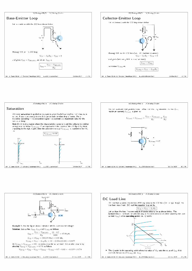
DC Biasing Circuits
Most common four common-emitter biasing circuits are given below
1. Fixed-Bias Circuit
2. Emitter-Stabilized Bias Circuit
3. Voltage Divider Bias Circuit
4. DC Bias with Voltage Feedback
Dr. U. Sezen & Dr. D. Gökçen (Hacettepe Uni.) ELE230 Electronics I 15-Mar-2017 5 / 59
DC Biasing of BJTs DC Biasing Circuits
Fixed-Bias CircuitFixed-bias circuit is given below
Let us start DC analysis by drawing the DC equivalent circuit as shown below
Dr. U. Sezen & Dr. D. Gökçen (Hacettepe Uni.) ELE230 Electronics I 15-Mar-2017 6 / 59
DC Biasing of BJTs DC Biasing Circuits
Base-Emitter Loop
Let us continue with the BE loop shown below
Writing KVL on the BE loop
VCC − IBRB − VBE = 0
and given VBE = VBE(ON), we obtain IBQ as
IBQ =VCC − VBE(ON)
RB
Dr. U. Sezen & Dr. D. Gökçen (Hacettepe Uni.) ELE230 Electronics I 15-Mar-2017 7 / 59
DC Biasing of BJTs DC Biasing Circuits
Collector-Emitter LoopLet us continue with the CE loop shown below
Writing KVL on the CE loop (i.e., DC load-line equation)
VCC − ICRC − VCE = 0
and given (assuming BJT is in active state)
ICQ = βIBQ
we obtain VCEQ as
VCEQ = VCC − ICQRC
Dr. U. Sezen & Dr. D. Gökçen (Hacettepe Uni.) ELE230 Electronics I 15-Mar-2017 8 / 59
DC Biasing of BJTs DC Biasing Circuits
Saturation
The term saturation is applied to any system where levels have reached their maximumvalues. A saturated sponge is one that cannot hold another drop of water. For atransistor operating in the saturation region, the current is a maximum value for theparticular design.
Note that it is in a region where the characteristic curves join and the collector-to-emittervoltage is at or below VCE(sat). If we approximate the curves of the left gure by thoseappearing in the right gure, then the saturation voltage VCE(sat) is assumed to be 0V,i.e,
VCE(sat)∼= 0V
Dr. U. Sezen & Dr. D. Gökçen (Hacettepe Uni.) ELE230 Electronics I 15-Mar-2017 9 / 59
DC Biasing of BJTs DC Biasing Circuits
For the xed-bias conguration shown below, the resulting saturation current (i.e.,maximum current) IC(sat) is given by
IC(sat) = IC(max) =VCC − VCE(sat)
RC∼=VCC
RC
Dr. U. Sezen & Dr. D. Gökçen (Hacettepe Uni.) ELE230 Electronics I 15-Mar-2017 10 / 59
DC Biasing of BJTs DC Biasing Circuits
Example 1: For the gure above, calculate all DC currents and voltages.
Solution: Let us nd IBQ, ICQ and VCEQ as follows
IBQ =VCC − VBE(ON)
RB=
12− 0.7
240k= 47.08µA,
ICQ = βIBQ = (50)(47.08µ) = 2.35mA,
VCEQ = VCC − ICQRC = 12− (2.35m)(2.2k) = 6.83V.
As VCEQ > VCE(sat) = 0V, transistor is in the active state. Let us also prove it byshowing VBCQ < VBC(ON) = 0.7V as follows
VBCQ = VBQ − VCQ = VBEQ − VCEQ = 0.7− 6.83 = −6.13V < 0.7V.
Dr. U. Sezen & Dr. D. Gökçen (Hacettepe Uni.) ELE230 Electronics I 15-Mar-2017 11 / 59
DC Biasing of BJTs DC Biasing Circuits
DC Load LineDC load line equation comes from KVL equation in the CE loop (i.e., output loop). Forthe xed-bias circuit, DC load line equation is given by
VCE = VCC − ICRCLet us draw the load line over output characteristics curve as shown below. Theintersection of the load-line with the output characteristics curve (determined by the basecurrent IBQ) is the operating point, i.e., Q-point.
I The Q-point is the operating point where the value of RB sets the value of IBQ thatcontrols the values of VCEQ and ICQ.
Dr. U. Sezen & Dr. D. Gökçen (Hacettepe Uni.) ELE230 Electronics I 15-Mar-2017 12 / 59
DC Biasing of BJTs DC Biasing Circuits
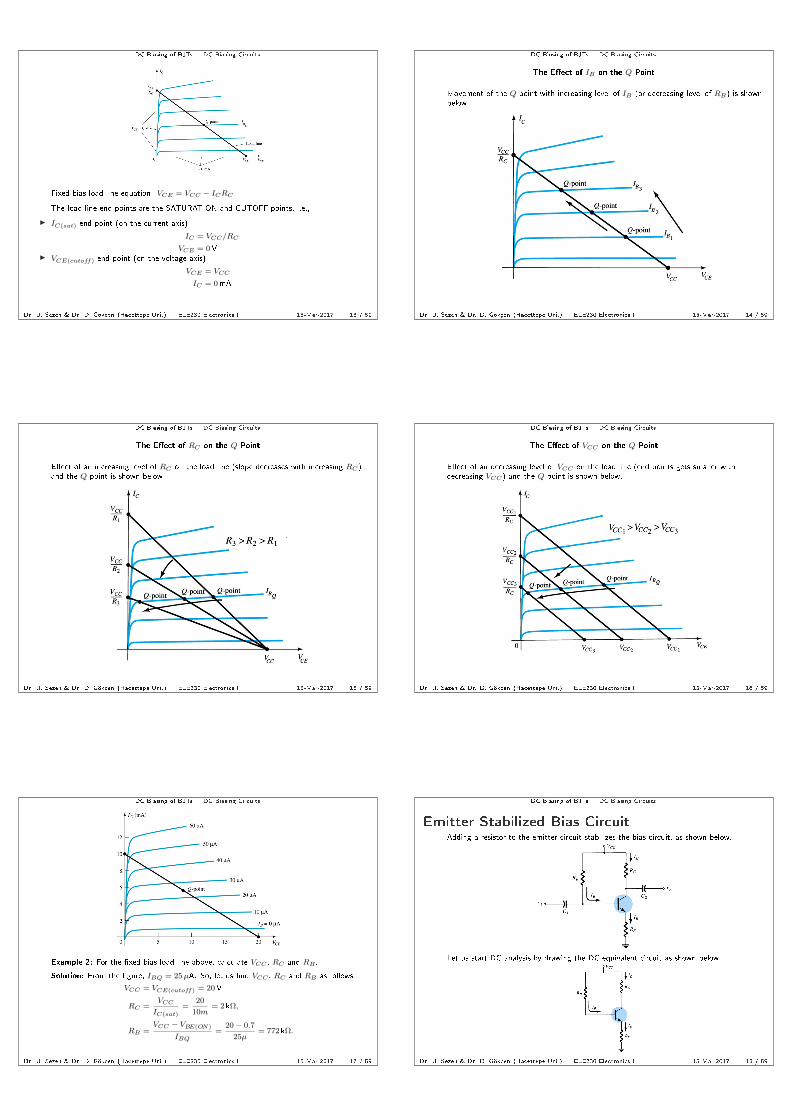
Fixed-bias load line equation: VCE = VCC − ICRC
The load line end points are the SATURATION and CUTOFF points, i.e.,
I IC(sat) end point (on the current axis):
IC = VCC/RC
VCE = 0VI VCE(cutoff) end point (on the voltage axis):
VCE = VCC
IC = 0mA
Dr. U. Sezen & Dr. D. Gökçen (Hacettepe Uni.) ELE230 Electronics I 15-Mar-2017 13 / 59
DC Biasing of BJTs DC Biasing Circuits
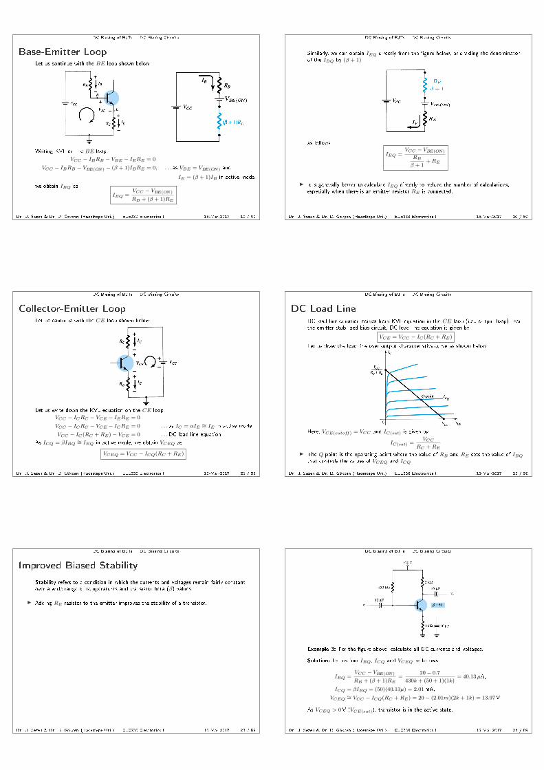
The Eect of IB on the Q-Point
Movement of the Q-point with increasing level of IB (or decreasing level of RB) is shownbelow.
Dr. U. Sezen & Dr. D. Gökçen (Hacettepe Uni.) ELE230 Electronics I 15-Mar-2017 14 / 59
DC Biasing of BJTs DC Biasing Circuits
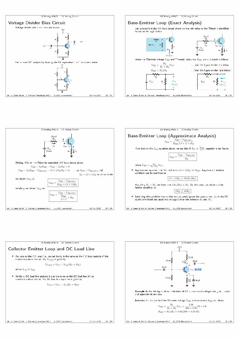
The Eect of RC on the Q-Point
Eect of an increasing level of RC on the load line (slope decreases with increasing RC)and the Q-point is shown below.
Dr. U. Sezen & Dr. D. Gökçen (Hacettepe Uni.) ELE230 Electronics I 15-Mar-2017 15 / 59
DC Biasing of BJTs DC Biasing Circuits
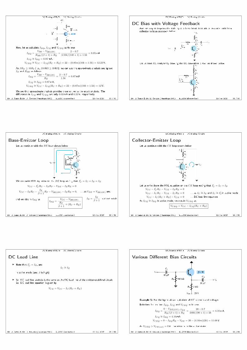
The Eect of VCC on the Q-Point
Eect of an decreasing level of VCC on the load line (end points gets smaller withdecreasing VCC) and the Q-point is shown below.
Dr. U. Sezen & Dr. D. Gökçen (Hacettepe Uni.) ELE230 Electronics I 15-Mar-2017 16 / 59
DC Biasing of BJTs DC Biasing Circuits
Example 2: For the xed-bias load line above, calculate VCC , RC and RB .
Solution: From the gure, IBQ = 25µA. So, let us nd VCC , RC and RB as follows
VCC = VCE(cutoff) = 20V,
RC =VCC
IC(sat)
=20
10m= 2 kΩ,
RB =VCC − VBE(ON)
IBQ=
20− 0.7
25µ= 772 kΩ.
Dr. U. Sezen & Dr. D. Gökçen (Hacettepe Uni.) ELE230 Electronics I 15-Mar-2017 17 / 59
DC Biasing of BJTs DC Biasing Circuits
Emitter-Stabilized Bias CircuitAdding a resistor to the emitter circuit stabilizes the bias circuit, as shown below.
Let us start DC analysis by drawing the DC equivalent circuit as shown below
Dr. U. Sezen & Dr. D. Gökçen (Hacettepe Uni.) ELE230 Electronics I 15-Mar-2017 18 / 59
DC Biasing of BJTs DC Biasing Circuits
Base-Emitter LoopLet us continue with the BE loop shown below
Writing KVL on the BE loop
VCC − IBRB − VBE − IERE = 0
VCC − IBRB − VBE(ON) − (β + 1)IBRE = 0, . . . as VBE = VBE(ON) and
IE = (β + 1)IB in active mode
we obtain IBQ as
IBQ =VCC − VBE(ON)
RB + (β + 1)RE
Dr. U. Sezen & Dr. D. Gökçen (Hacettepe Uni.) ELE230 Electronics I 15-Mar-2017 19 / 59
DC Biasing of BJTs DC Biasing Circuits
Similarly, we can obtain IEQ directly from the gure below, or dividing the denominatorof the IBQ by (β + 1)
as follows
IEQ =VCC − VBE(ON)
RB
β + 1+RE
I It is generally better to calculate IEQ directly to reduce the number of calculations,especially when there is an emitter resistor RE is connected.
Dr. U. Sezen & Dr. D. Gökçen (Hacettepe Uni.) ELE230 Electronics I 15-Mar-2017 20 / 59
DC Biasing of BJTs DC Biasing Circuits
Collector-Emitter LoopLet us continue with the CE loop shown below
Let us write down the KVL equation on the CE loop
VCC − ICRC − VCE − IERE = 0
VCC − ICRC − VCE − ICRE = 0 . . . as IC = αIE ∼= IE in active mode
VCC − IC(RC +RE)− VCE = 0 . . .DC load line equation
As ICQ = βIBQ ∼= IEQ in active mode, we obtain VCEQ as
VCEQ = VCC − ICQ(RC +RE)
Dr. U. Sezen & Dr. D. Gökçen (Hacettepe Uni.) ELE230 Electronics I 15-Mar-2017 21 / 59
DC Biasing of BJTs DC Biasing Circuits
DC Load LineDC load line equation comes from KVL equation in the CE loop (i.e., output loop). Forthe emitter-stabilized bias circuit, DC load line equation is given by
VCE = VCC − IC(RC +RE)
Let us draw the load line over output characteristics curve as shown below.
Here, VCE(cutoff) = VCC and IC(sat) is given by
IC(sat) =VCC
RC +REI The Q-point is the operating point where the value of RB and RE sets the value of IBQ
that controls the values of VCEQ and ICQ.
Dr. U. Sezen & Dr. D. Gökçen (Hacettepe Uni.) ELE230 Electronics I 15-Mar-2017 22 / 59
DC Biasing of BJTs DC Biasing Circuits
Improved Biased Stability
Stability refers to a condition in which the currents and voltages remain fairly constantover a wide range of temperatures and transistor beta (β) values.
I Adding RE resistor to the emitter improves the stability of a transistor.
Dr. U. Sezen & Dr. D. Gökçen (Hacettepe Uni.) ELE230 Electronics I 15-Mar-2017 23 / 59
DC Biasing of BJTs DC Biasing Circuits
Example 3: For the gure above, calculate all DC currents and voltages.
Solution: Let us nd IBQ, ICQ and VCEQ as follows
IBQ =VCC − VBE(ON)
RB + (β + 1)RE=
20− 0.7
430k + (50 + 1)(1k)= 40.13µA,
ICQ = βIBQ = (50)(40.13µ) = 2.01mA,
VCEQ ∼= VCC − ICQ(RC +RE) = 20− (2.01m)(2k + 1k) = 13.97V.
As VCEQ > 0V (VCE(sat)), transistor is in the active state.
Dr. U. Sezen & Dr. D. Gökçen (Hacettepe Uni.) ELE230 Electronics I 15-Mar-2017 24 / 59
DC Biasing of BJTs DC Biasing Circuits
Voltage Divider Bias CircuitVoltage divider bias circuit is given below
Let us start DC analysis by drawing the DC equivalent circuit as shown below
Dr. U. Sezen & Dr. D. Gökçen (Hacettepe Uni.) ELE230 Electronics I 15-Mar-2017 25 / 59
DC Biasing of BJTs DC Biasing Circuits
Base-Emitter Loop (Exact Analysis)Let us transform the BE loop circuit shown on the left below to the Thévenin simpliedcircuit on the right below
where the Thévenin voltage VBB and Thévenin resistance RBB are calculated as follows
VBB =R2
R1 +R2VCC . . . from the gure on the left below
RBB = R1||R2 . . . from the gure on the right below
Dr. U. Sezen & Dr. D. Gökçen (Hacettepe Uni.) ELE230 Electronics I 15-Mar-2017 26 / 59
DC Biasing of BJTs DC Biasing Circuits
Writing KVL on the Thévenin equivalent BE loop shown above
VBB − IBRBB − VBE − IERE = 0
VBB − IBRBB − VBE(ON) − (β + 1)IBRE = 0, . . . as VBE = VBE(ON) and
IE = (β + 1)IB in active mode
we obtain IBQ as
IBQ =VBB − VBE(ON)
RBB + (β + 1)RE
Similarly, we obtain IEQ as
IEQ =VBB − VBE(ON)
RBB
β + 1+RE
Dr. U. Sezen & Dr. D. Gökçen (Hacettepe Uni.) ELE230 Electronics I 15-Mar-2017 27 / 59
DC Biasing of BJTs DC Biasing Circuits
Base-Emitter Loop (Approximate Analysis)IEQ =
VBB − VBE(ON)
RBB/(β + 1) +RE
If we look at the IEQ equation above, we see that if RE RBBβ+1
, equation simplies to
IEQ =VBB − VBE(ON)
RE
where VBB = R2R1+R2
VCC .
I Approximate approach can be used when (β + 1)RE RBB . Approximate analysiscondition can be rewritten as
(β + 1)RE ≥ 10(R1||R2).
Assuming R1 > R2, we know that (R1||R2) ≤ R2. So, the condition above can befurther simplied to
βRE ≥ 10R2.
I Satisfying this condition means that we can safely ignore the base current IB in the DCequivalent circuit and apply the voltage divider rule between R2 and R1.
Dr. U. Sezen & Dr. D. Gökçen (Hacettepe Uni.) ELE230 Electronics I 15-Mar-2017 28 / 59
DC Biasing of BJTs DC Biasing Circuits
Collector-Emitter Loop and DC Load Line
I Analysis on the CE loop (i.e., output loop), is the same as the CE loop analysis of theemitter-stabilized circuit. So, VCEQ is given by
VCEQ = VCC − ICQ(RC +RE)
where ICQ ∼= IEQ.
I Similarly, DC load line analysis is also the same as the DC load line of theemitter-stabilized circuit. So, DC load line equation is given by
VCE = VCC − IC(RC +RE)
Dr. U. Sezen & Dr. D. Gökçen (Hacettepe Uni.) ELE230 Electronics I 15-Mar-2017 29 / 59
DC Biasing of BJTs DC Biasing Circuits
Example 4: For the gure above, calculate all DC currents and voltages using both exactand approximate analysis.
Solution: Let us rst nd the Thévenin voltage VBB and resistance RBB as follows
VBB =R2
R1 +R2VCC =
3.9k
39k + 3.9k22 = 2V,
RBB = R1||R2 = 3.9k||39k = 3.55 kΩ.
Dr. U. Sezen & Dr. D. Gökçen (Hacettepe Uni.) ELE230 Electronics I 15-Mar-2017 30 / 59
DC Biasing of BJTs DC Biasing Circuits
Now, let us calculate IBQ, ICQ and VCEQ as follows
IEQ =VBB − VBE(ON)
RBB/(β + 1) +RE=
2− 0.7
3.55k/(140 + 1) + 1.5k= 0.85mA,
ICQ ∼= IEQ = 0.85mA,
VCEQ ∼= VCC − ICQ(RC +RE) = 22− (0.85m)(10k + 1.5k) = 12.23V.
As βRE ≥ 10R2 (i.e., 210 kΩ ≥ 39 kΩ), we can use the approximate analysis and ignoreIB and RBB as follows
IEQ =VBB − VBE(ON)
RE=
2− 0.7
1.5k= 0.87mA,
ICQ ∼= IEQ = 0.87mA,
VCEQ ∼= VCC − ICQ(RC +RE) = 22− (0.87m)(10k + 1.5k) = 12V.
We see that approximate analysis provides close values to the exact analysis. Thedierences in ICQ and VCEQ are only 0.02mA and 0.23V, respectively.
Dr. U. Sezen & Dr. D. Gökçen (Hacettepe Uni.) ELE230 Electronics I 15-Mar-2017 31 / 59
DC Biasing of BJTs DC Biasing Circuits
DC Bias with Voltage FeedbackAnother way to improve the stability of a bias circuit is to add a feedback path fromcollector to base as shown below
Let us start DC analysis by drawing the DC equivalent circuit as shown below
Dr. U. Sezen & Dr. D. Gökçen (Hacettepe Uni.) ELE230 Electronics I 15-Mar-2017 32 / 59
DC Biasing of BJTs DC Biasing Circuits
Base-Emitter LoopLet us continue with the BE loop shown below
We can write KVL equation on the BE loop noting that I′C = IC + IB = IE
VCC − I′CRC − IBRF − VBE − IERE = 0
VCC − IERC −IE
β + 1RF − VBE(ON) − IERE = 0, . . . as VBE = VBE(ON) and
IB =IE
β + 1in active modeand we obtain IEQ as
IEQ =VCC − VBE(ON)
RF
β + 1+ (RC +RE)
Dr. U. Sezen & Dr. D. Gökçen (Hacettepe Uni.) ELE230 Electronics I 15-Mar-2017 33 / 59
DC Biasing of BJTs DC Biasing Circuits
Collector-Emitter LoopLet us continue with the CE loop shown below
Let us write down the KVL equation on the CE loop noting that I′C = IC + IB
VCC − I′CRC − VCE − IERE = 0
VCC − ICRC − VCE − ICRE = 0 . . . as IC ∼= IE and IC ∼= I′C in active mode
VCC − IC(RC +RE)− VCE = 0 . . .DC load line equation
As ICQ ∼= IEQ in active mode, we obtain VCEQ as
VCEQ = VCC − ICQ(RC +RE)
Dr. U. Sezen & Dr. D. Gökçen (Hacettepe Uni.) ELE230 Electronics I 15-Mar-2017 34 / 59
DC Biasing of BJTs DC Biasing Circuits
DC Load Line
I Note that I′C = IE , andIC ∼= IE
in active mode (and β is high).
I So, DC load line analysis is the same as the DC load line of the emitter-stabilized circuit.So, DC load line equation is given by
VCE = VCC − IC(RC +RE)
Dr. U. Sezen & Dr. D. Gökçen (Hacettepe Uni.) ELE230 Electronics I 15-Mar-2017 35 / 59
DC Biasing of BJTs DC Biasing Circuits
Various Dierent Bias Circuits
Example 5: For the gure above, calculate all DC currents and voltages.
Solution: Let us nd IEQ, ICQ and VCEQ as follows
IEQ =0− VBE(ON)−VEE
RB/(β + 1) +RE=
20− 0.7
240k/(90 + 1) + 2k= 4.16mA,
ICQ ∼= IEQ = 4.16mA,
VCEQ = 0− IEQRE − VEE = 20− (4.16m)(2k) = 11.68V.
As VCEQ > VCE(sat) = 0V, transistor is in the active state.
Dr. U. Sezen & Dr. D. Gökçen (Hacettepe Uni.) ELE230 Electronics I 15-Mar-2017 36 / 59
DC Biasing of BJTs DC Biasing Circuits
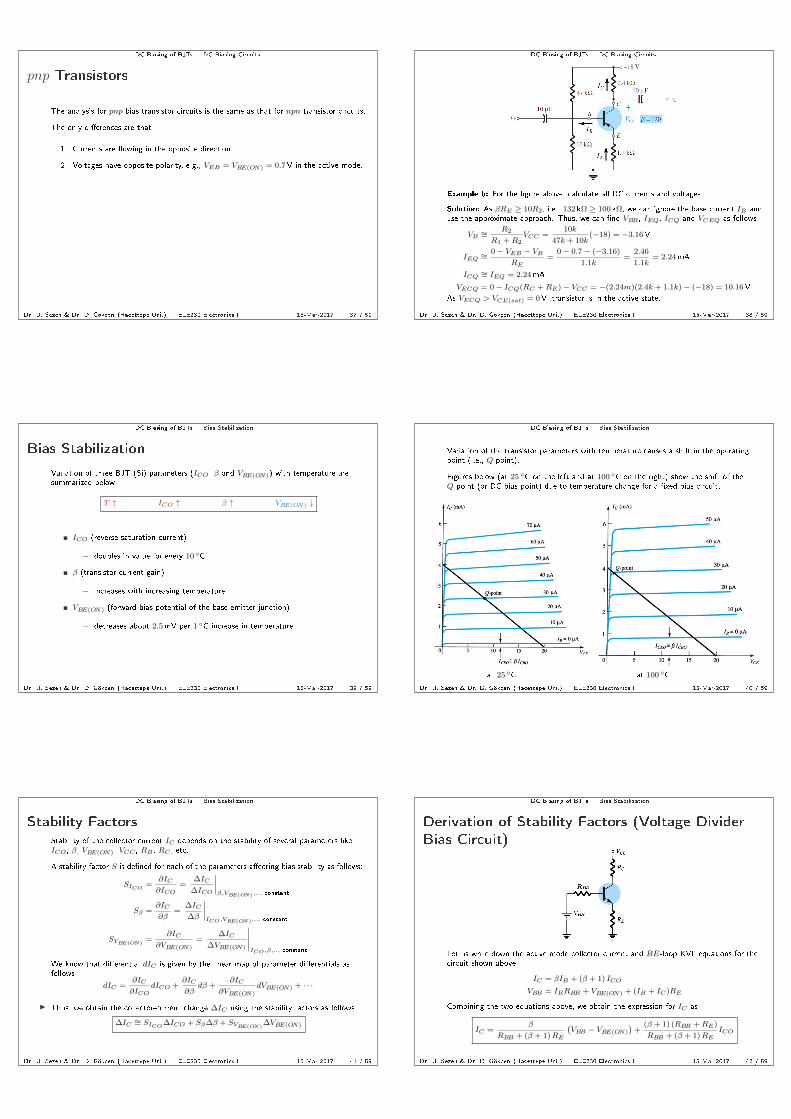
pnp Transistors
The analysis for pnp bias transistor circuits is the same as that for npn transistor circuits.
The only dierences are that
1. Currents are owing in the opposite direction.
2. Voltages have opposite polarity, e.g., VEB = VBE(ON) = 0.7V in the active mode.
Dr. U. Sezen & Dr. D. Gökçen (Hacettepe Uni.) ELE230 Electronics I 15-Mar-2017 37 / 59
DC Biasing of BJTs DC Biasing Circuits
Example 6: For the gure above, calculate all DC currents and voltages.
Solution: As βRE ≥ 10R2, i.e., 132 kΩ ≥ 100 kΩ, we can ignore the base current IB anduse the approximate approach. Thus, we can nd VBB , IEQ, ICQ and VCEQ as follows
VB ∼=R2
R1 +R2VCC =
10k
47k + 10k(−18) = −3.16V
IEQ ∼=0− VEB − VB
RE=
0− 0.7− (−3.16)
1.1k=
2.46
1.1k= 2.24mA,
ICQ ∼= IEQ = 2.24mA,
VECQ = 0− ICQ(RC +RE)− VCC = −(2.24m)(2.4k + 1.1k)− (−18) = 10.16V.
As VECQ > VCE(sat) = 0V, transistor is in the active state.
Dr. U. Sezen & Dr. D. Gökçen (Hacettepe Uni.) ELE230 Electronics I 15-Mar-2017 38 / 59
DC Biasing of BJTs Bias Stabilization
Bias Stabilization
Variation of three BJT (Si) parameters (ICO, β and VBE(ON)) with temperature aresummarized below
T ↑ ICO ↑ β ↑ VBE(ON) ↓
ICO (reverse saturation current)
− doubles in value for every 10 C
β (transistor current gain)
− increases with increasing temperature
VBE(ON) (forward bias potential of the base-emitter junction)
− decreases about 2.5mV per 1 C increase in temperature
Dr. U. Sezen & Dr. D. Gökçen (Hacettepe Uni.) ELE230 Electronics I 15-Mar-2017 39 / 59
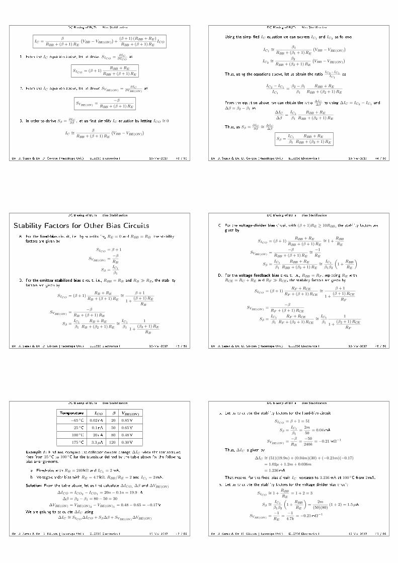
DC Biasing of BJTs Bias Stabilization
Variation of the transistor parameters with temperature causes a shift in the operatingpoint (i.e., Q-point).
Figures below (at 25 C on the left and at 100 C on the right) show the shift of theQ-point (or DC bias point) due to temperature change for a xed-bias circuit.
at 25 C at 100 C
Dr. U. Sezen & Dr. D. Gökçen (Hacettepe Uni.) ELE230 Electronics I 15-Mar-2017 40 / 59
DC Biasing of BJTs Bias Stabilization
Stability FactorsStability of the collector current IC depends on the stability of several parameters likeICO, β, VBE(ON), VCC , RB , RC , etc.
A stability factor S is dened for each of the parameters aecting bias stability as follows:
SICO=
∂IC
∂ICO=
∆IC
∆ICO
∣∣∣∣β,VBE(ON),... constant
Sβ =∂IC
∂β=
∆IC
∆β
∣∣∣∣ICO,VBE(ON),... constant
SVBE(ON)=
∂IC
∂VBE(ON)
=∆IC
∆VBE(ON)
∣∣∣∣∣ICO,β,... constant
We know that dierential dIC is given by the linear map of parameter dierentials asfollows
dIC =∂IC
∂ICOdICO +
∂IC
∂βdβ +
∂IC
∂VBE(ON)
dVBE(ON) + · · ·
I Thus, we obtain the collector-current change ∆IC using the stability factors as follows
∆IC ∼= SICO∆ICO + Sβ∆β + SVBE(ON)
∆VBE(ON)
Dr. U. Sezen & Dr. D. Gökçen (Hacettepe Uni.) ELE230 Electronics I 15-Mar-2017 41 / 59
DC Biasing of BJTs Bias Stabilization
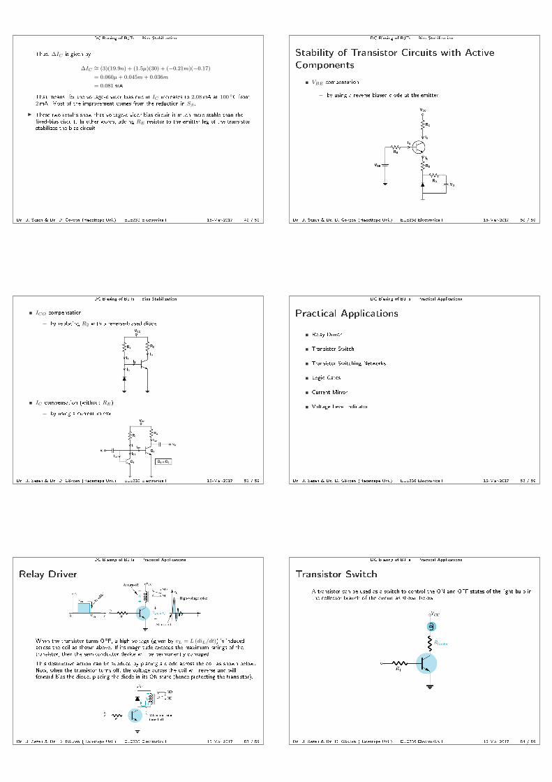
Derivation of Stability Factors (Voltage-DividerBias Circuit)
Let us write down the active mode collector current and BE-loop KVL equations for thecircuit shown above,
IC = βIB + (β + 1) ICO
VBB = IBRBB + VBE(ON) + (IB + IC)RE
Combining the two equations above, we obtain the expression for IC as
IC =β
RBB + (β + 1)RE
(VBB − VBE(ON)
)+
(β + 1) (RBB +RE)
RBB + (β + 1)REICO
Dr. U. Sezen & Dr. D. Gökçen (Hacettepe Uni.) ELE230 Electronics I 15-Mar-2017 42 / 59
DC Biasing of BJTs Bias Stabilization
IC =β
RBB + (β + 1)RE
(VBB − VBE(ON)
)+
(β + 1) (RBB +RE)
RBB + (β + 1)REICO
1. From the IC equation above, let us derive SICO= ∂IC
∂ICOas
SICO= (β + 1)
RBB +RE
RBB + (β + 1)RE
2. From the IC equation above, let us derive SVBE(ON)= ∂IC
∂VBE(ON)as
SVBE(ON)=
−βRBB + (β + 1)RE
3. In order to derive Sβ = ∂IC∂β
, let us rst simplify IC equation by letting ICO ∼= 0
IC ∼=β
RBB + (β + 1)RE
(VBB − VBE(ON)
)
Dr. U. Sezen & Dr. D. Gökçen (Hacettepe Uni.) ELE230 Electronics I 15-Mar-2017 43 / 59
DC Biasing of BJTs Bias Stabilization
Using the simplied IC equation we can express IC1and IC2
as follows
IC1∼=
β1
RBB + (β1 + 1)RE
(VBB − VBE(ON)
)IC2∼=
β2
RBB + (β2 + 1)RE
(VBB − VBE(ON)
)Thus, using the equations above, let us obrain the ratio
IC2−IC1IC1
as
IC2− IC1
IC1
=β2 − β1
β1
RBB +RE
RBB + (β2 + 1)RE
From the equation above, we can obtain the ratio ∆IC∆β
by using ∆IC = IC2 − IC1 and
∆β = β2 − β1 as∆IC
∆β=IC1
β1
RBB +RE
RBB + (β2 + 1)RE
Thus, as Sβ = ∂IC∂β∼= ∆IC
∆β
Sβ =IC1
β1
RBB +RE
RBB + (β2 + 1)RE
Dr. U. Sezen & Dr. D. Gökçen (Hacettepe Uni.) ELE230 Electronics I 15-Mar-2017 44 / 59
DC Biasing of BJTs Bias Stabilization
Stability Factors for Other Bias Circuits
A. For the xed-bias circuit, i.e., by substituting RE = 0 and RBB = RB , the stabilityfactors are given by
SICO= β + 1
SVBE(ON)=−βRB
Sβ =IC1
β1
B. For the emitter-stabilized bias circuit, i.e., RBB = RB and RB RE , the stabilityfactors are given by
SICO= (β + 1)
RB +RE
RB + (β + 1)RE∼=
β + 1
1 +(β + 1)RE
RB
SVBE(ON)=
−βRB + (β + 1)RE
Sβ =IC1
β1
RB +RE
RB + (β2 + 1)RE∼=IC1
β1
1
1 +(β2 + 1)RE
RB
Dr. U. Sezen & Dr. D. Gökçen (Hacettepe Uni.) ELE230 Electronics I 15-Mar-2017 45 / 59
DC Biasing of BJTs Bias Stabilization
C. For the voltage-divider bias circuit with (β + 1)RE ≥ 10RBB , the stability factors aregiven by
SICO= (β + 1)
RBB +RE
RBB + (β + 1)RE∼= 1 +
RBB
RE
SVBE(ON)=
−βRBB + (β + 1)RE
∼=−1
RE
Sβ =IC1
β1
RBB +RE
RBB + (β2 + 1)RE∼=
IC1
β1β2
(1 +
RBB
RE
)D. For the voltage-feedback bias circuit, i.e., RBB = RF , replacing RE with
RCE = RC +RE and RF RCE , the stability factors are given by
SICO= (β + 1)
RF +RCE
RF + (β + 1)RCE∼=
β + 1
1 +(β + 1)RCE
RF
SVBE(ON)=
−βRF + (β + 1)RCE
Sβ =IC1
β1
RF +RCE
RF + (β2 + 1)RCE∼=IC1
β1
1
1 +(β2 + 1)RCE
RF
Dr. U. Sezen & Dr. D. Gökçen (Hacettepe Uni.) ELE230 Electronics I 15-Mar-2017 46 / 59
DC Biasing of BJTs Bias Stabilization
Temperature ICO β VBE(ON)
−65 C 0.02 nA 20 0.85V
25 C 0.1 nA 50 0.65V
100 C 20 nA 80 0.48V
175 C 3.3µA 120 0.30V
Example 7: Find and compare the collector current change ∆IC when the temperaturerises from 25 C to 100 C for the transistor dened by the table above for the followingbias arrangements.
a. Fixed-bias with RB = 240 kΩ and IC1 = 2mA,
b. Voltage-divider bias with RE = 4.7 kΩ, RBB/RE = 2 and IC1 = 2mA.
Solution: From the table above, let us rst calculate ∆ICO, ∆β and ∆VBE(ON)
∆ICO = ICO2 − ICO1 = 20n− 0.1n = 19.9 nA
∆β = β2 − β1 = 80− 50 = 30
∆VBE(ON) = VBE(ON)2 − VBE(ON)1 = 0.48− 0.65 = −0.17V
We are goiung to calculate ∆IC using
∆IC ∼= SICO∆ICO + Sβ∆β + SVBE(ON)
∆VBE(ON)
Dr. U. Sezen & Dr. D. Gökçen (Hacettepe Uni.) ELE230 Electronics I 15-Mar-2017 47 / 59
DC Biasing of BJTs Bias Stabilization
a. Let us calculate the stability factors for the xed-bias circuit
SICO= β + 1 = 51
Sβ =IC1
β1=
2m
50= 0.04mA
SVBE(ON)=−βRB
=−50
240k= −0.21mΩ−1
Thus, ∆IC is given by
∆IC ∼= (51)(19.9n) + (0.04m)(30) + (−0.21m)(−0.17)
= 1.02µ+ 1.2m+ 0.036m
= 1.236mA
That means, for the xed-bias circuit IC increases to 3.236mA at 100 C from 2mA.
b. Let us calculate the stability factors for the voltage-divider bias circuit
SICO∼= 1 +
RBB
RE= 1 + 2 = 3
Sβ ∼=IC1
β1β2
(1 +
RBB
RE
)=
2m
(50)(80)(1 + 2) = 1.5µA
SVBE(ON)=−1
RE=−1
4.7k= −0.21mΩ−1
Dr. U. Sezen & Dr. D. Gökçen (Hacettepe Uni.) ELE230 Electronics I 15-Mar-2017 48 / 59
DC Biasing of BJTs Bias Stabilization
Thus, ∆IC is given by
∆IC ∼= (3)(19.9n) + (1.5µ)(30) + (−0.21m)(−0.17)
= 0.060µ+ 0.045m+ 0.036m
= 0.081mA
That means, for the voltage-divider bias circuit IC increases to 2.08mA at 100 C from2mA. Most of the improvement comes from the reduction in Sβ .
I These two results show that voltage-divider bias circuit is much more stable than thexed-bias circuit. In other words, adding RE resistor to the emitter leg of the transistorstabilizes the bias circuit.
Dr. U. Sezen & Dr. D. Gökçen (Hacettepe Uni.) ELE230 Electronics I 15-Mar-2017 49 / 59
DC Biasing of BJTs Bias Stabilization
Stability of Transistor Circuits with ActiveComponents
VBE compensation
− by using a reverse-biased diode at the emitter
Dr. U. Sezen & Dr. D. Gökçen (Hacettepe Uni.) ELE230 Electronics I 15-Mar-2017 50 / 59
DC Biasing of BJTs Bias Stabilization
ICO compensation
− by replacing R2 with a reverse-biased diode
IC compensation (without RE)
− by using a current mirror
Dr. U. Sezen & Dr. D. Gökçen (Hacettepe Uni.) ELE230 Electronics I 15-Mar-2017 51 / 59
DC Biasing of BJTs Practical Applications
Practical Applications
Relay Driver
Transistor Switch
Transistor Switching Networks
Logic Gates
Current Mirror
Voltage Level Indicator
Dr. U. Sezen & Dr. D. Gökçen (Hacettepe Uni.) ELE230 Electronics I 15-Mar-2017 52 / 59
DC Biasing of BJTs Practical Applications
Relay Driver
When the transistor turns OFF, a high voltage (given by vL = L (diL/dt)) is inducedacross the coil as shown above. If its magnitude exceeds the maximum ratings of thetransistor, then the semiconductor device will be permanently damaged.
This destructive action can be subdued by placing a diode across the coil as shown below.Now, when the transistor turns o, the voltage across the coil will reverse and willforward-bias the diode, placing the diode in its ON state (hence protecting the transistor).
Dr. U. Sezen & Dr. D. Gökçen (Hacettepe Uni.) ELE230 Electronics I 15-Mar-2017 53 / 59
DC Biasing of BJTs Practical Applications
Transistor Switch
A transistor can be used as a switch to control the ON and OFF states of the light-bulb inthe collector branch of the circuit as shown below.
Dr. U. Sezen & Dr. D. Gökçen (Hacettepe Uni.) ELE230 Electronics I 15-Mar-2017 54 / 59
DC Biasing of BJTs Practical Applications
Transistor Switching Networks
Transistors can also be used as switches for computer and control applications. Thecircuit shown above can be employed an inverter in computer logic circuitry.
Inversion process requires that the Q-point switch from cuto (Vo = VCE(cutoff) = 5V)to saturation (Vo = VCE(sat) = 0V) along the load line depicted below.
Dr. U. Sezen & Dr. D. Gökçen (Hacettepe Uni.) ELE230 Electronics I 15-Mar-2017 55 / 59
DC Biasing of BJTs Practical Applications
The total time required for the transistor to switch from the OFF to the ON state isdesignated as ton, and he total time required for a transistor to switch from the ON tothe OFF state is referred to as toff as shown below. ton and toff are dened by
ton = tr + td
toff = ts + tfwhere tr is the rise time from 10% to 90% of the output, td is the delay time between thechanging state of the input and the beginning of a response at the output, ts is thestorage time and and tf the fall time from 90% to 10% of the output.
Dr. U. Sezen & Dr. D. Gökçen (Hacettepe Uni.) ELE230 Electronics I 15-Mar-2017 56 / 59
DC Biasing of BJTs Practical Applications
Logic Gates
The gure above shows a BJT logic OR gate, and similarly The gure below shows a BJTlogic AND gate.
Dr. U. Sezen & Dr. D. Gökçen (Hacettepe Uni.) ELE230 Electronics I 15-Mar-2017 57 / 59
DC Biasing of BJTs Practical Applications
Current Mirror
The current mirror shown below is a DC circuit in which the current through a load iscontrolled by a current at another point in the circuit. That is, the current through theload is indepedent of the load.
Homework 1: For the gure above, show that the load current is equal to the loadcontrol current and given by
IL ∼= Icontrol =VCC − VBE(ON)
R
where the transistors are identical (Q1 ≡ Q2), i.e., VBE1(ON) = VBE2(ON) = VBE(ON)
and β1 = β2 = β, and current gain β is high, e.g., β ≥ 100.
Dr. U. Sezen & Dr. D. Gökçen (Hacettepe Uni.) ELE230 Electronics I 15-Mar-2017 58 / 59
DC Biasing of BJTs Practical Applications
Voltage Level IndicatorThe voltage level indicator circuit uses a green LED to indicate when the source voltage isclose to its monitoring level of 9V. The potentiometer is set to establish 5.4V at thepoint indicated below. The result is sucient voltage to turn on both the 4.7V Zener andthe transistor and establish a collector current through the LED sucient in magnitude toturn on the green LED. The LED will immediately turn o, revealing that the supplyvoltage has dropped below 9V or that the power source has been disconnected (i.e., whenthe voltage set up by the voltage divider circuit drops below 5.4V).
Dr. U. Sezen & Dr. D. Gökçen (Hacettepe Uni.) ELE230 Electronics I 15-Mar-2017 59 / 59