Embed Size (px)
Citation preview
ESE319 Introduction to Microelectronics
12009 Kenneth R. Laker, update 24Sep10
BJT Biasing Cont.● Biasing for DC Operating Point Stability● BJT Bias Using Emitter Negative Feedback● Single Supply BJT Bias Scheme● Constant Current BJT Bias Scheme● “Rule of Thumb” BJT Bias Design
ESE319 Introduction to Microelectronics
22009 Kenneth R. Laker, update 24Sep10
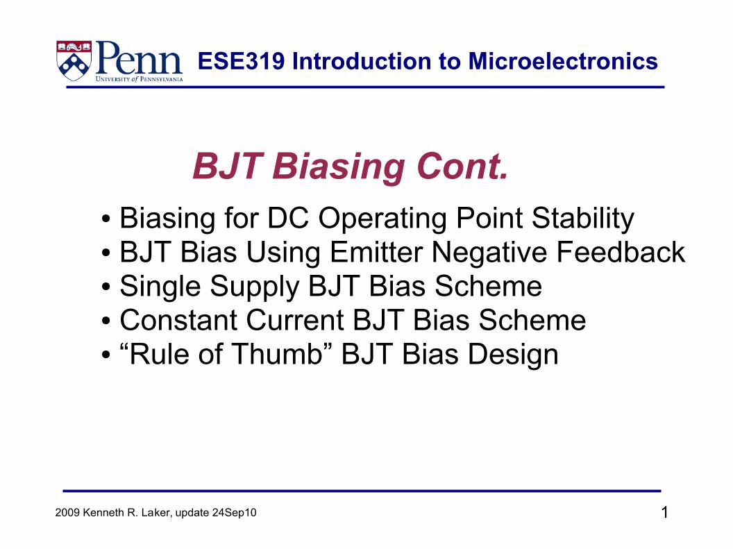
Previous Simple Base Biasing Schemes
What's wrong with these schemes?
ESE319 Introduction to Microelectronics
32009 Kenneth R. Laker, update 24Sep10
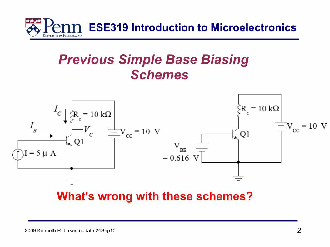
Biasing for Operating Point StabilityA practical biasing scheme must be insensitive to changes in transistor β and operating temperature! Negative feedback is one solution.
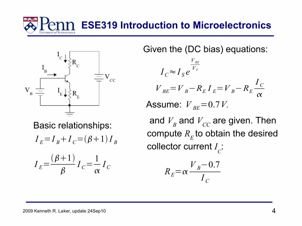
IC
IB
IE R
E
RC
VCC
VB
ESE319 Introduction to Microelectronics
42009 Kenneth R. Laker, update 24Sep10
I C≈ I S eV BE
V T
V BE=V B−RE I E=V B−RE
I C
Basic relationships:I E=I B I C=1 I B
I E=1
I C=
1
I C
Given the (DC bias) equations:
Assume: V BE=0.7V.
and VB and VCC are given. Thencompute RE to obtain the desiredcollector current I
C:
RE=V B−0.7
I C
ESE319 Introduction to Microelectronics
52009 Kenneth R. Laker, update 24Sep10
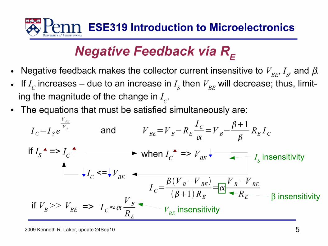
● Negative feedback makes the collector current insensitive to VBE, IS, and β. ● If IC increases – due to an increase in IS then VBE will decrease; thus, limit-
ing the magnitude of the change in IC.
● The equations that must be satisfied simultaneously are:
Negative Feedback via RE
I C=V B−V BE1RE
=V B−V BE
RE
V BE=V B−REI C
=V B−
1
RE I CI C=I S eV BE
V T and
if IS => IC when IC => VBE
IC <= VBE
IS insensitivity
β insensitivityif VB >> VBE VBE insensitivityI C≈
V B
RE=>
ESE319 Introduction to Microelectronics
62009 Kenneth R. Laker, update 24Sep10
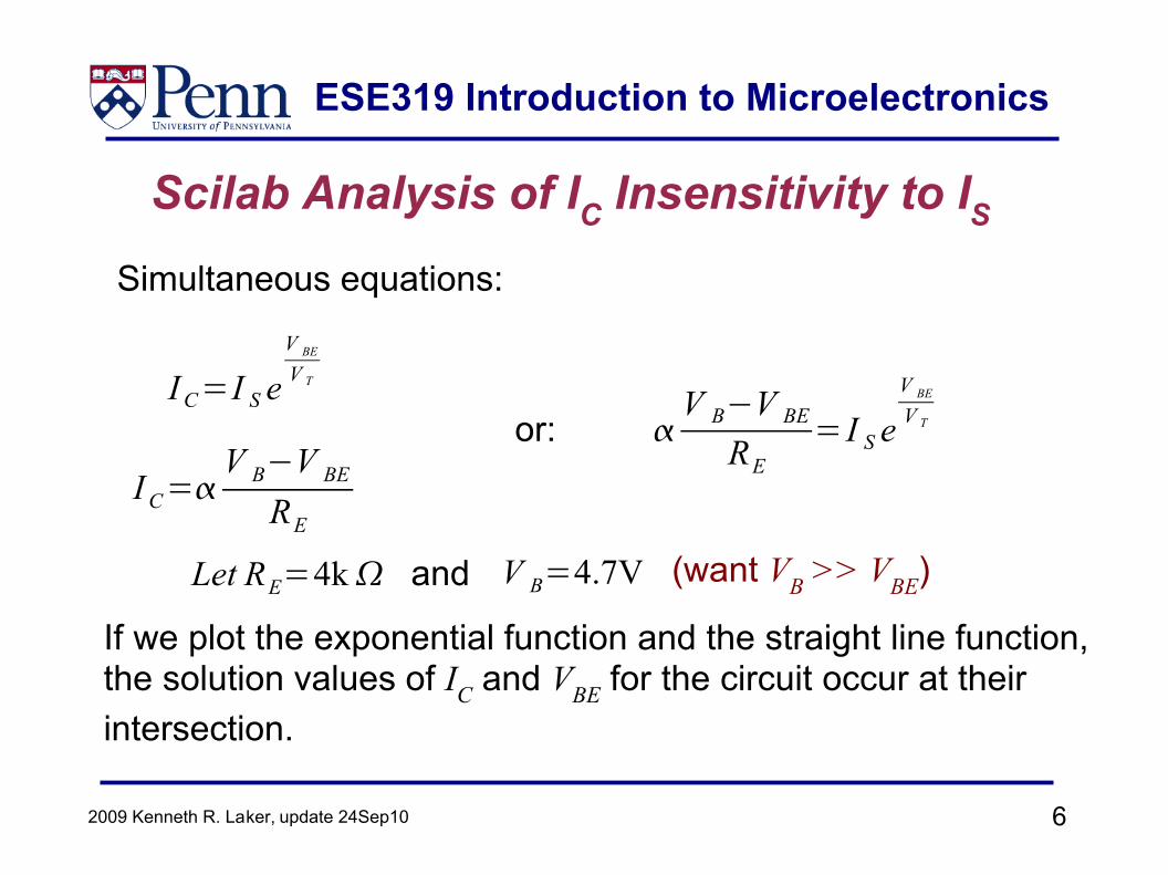
Scilab Analysis of IC Insensitivity to ISSimultaneous equations:
I C=I S eV BE
V T
I C=V B−V BE
RE
or: V B−V BE
RE= I S e
V BE
V T
If we plot the exponential function and the straight line function,the solution values of IC and VBE for the circuit occur at theirintersection.
Let RE=4k V B=4.7Vand (want VB >> VBE)

ESE319 Introduction to Microelectronics
72009 Kenneth R. Laker, update 24Sep10
Scilab Program//Calculate and plot npn BJT bias characteristicbeta=100;alpha=beta/(beta+1);VsubT=0.025;VTinv=1/VsubT;VBB=4.7;Re=4;vBE=0.0:0.01:1;iCline=alpha*(VBB-vBE)/Re;//mA.plot(vBE,iCline);iC=0.01:0.01:2; //mA.!IsubS =1E-16; //mA.for k= 1:1:8 IsubS=10*IsubS; vBE2=VsubT*log(iC/IsubS); plot(vBE2,iC); //Current in mA.end
I C=V B−V BE
RE
V BE=V T lnI C
I S
ESE319 Introduction to Microelectronics
82009 Kenneth R. Laker, update 24Sep10
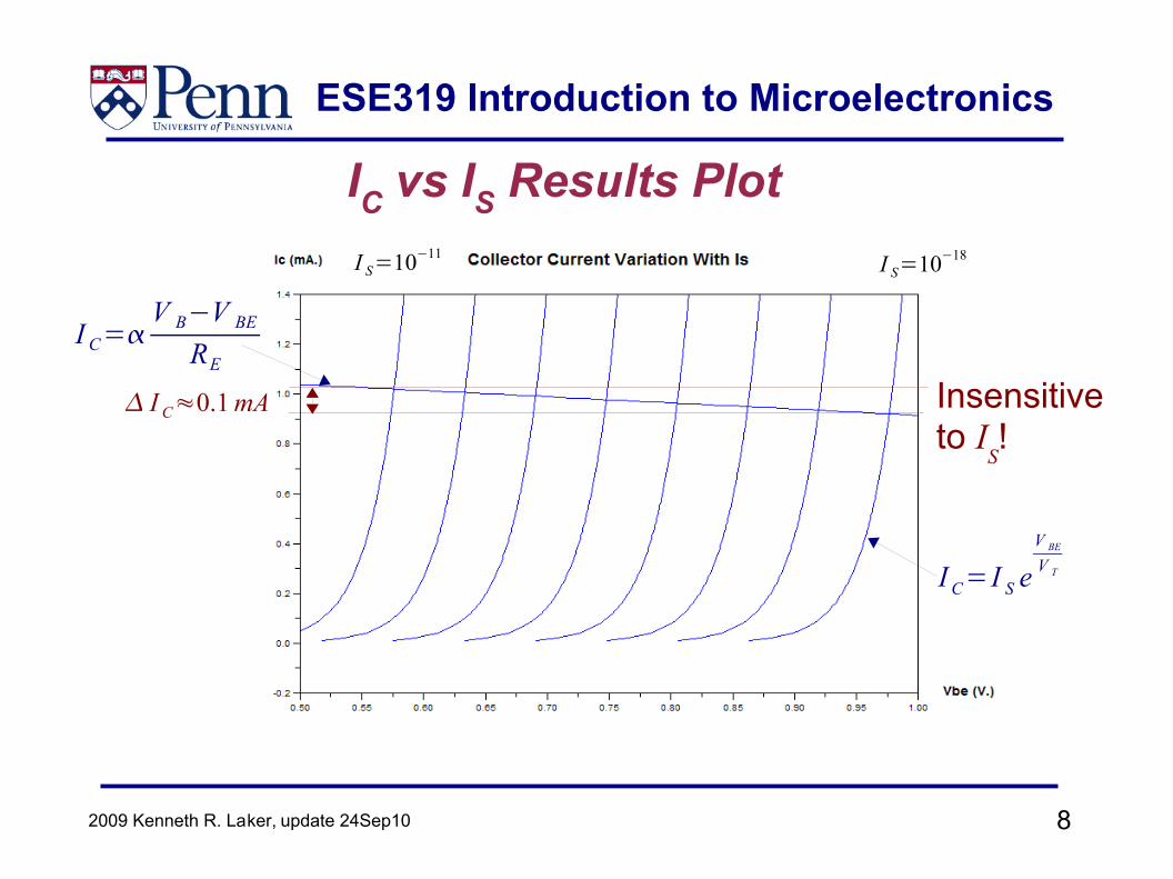
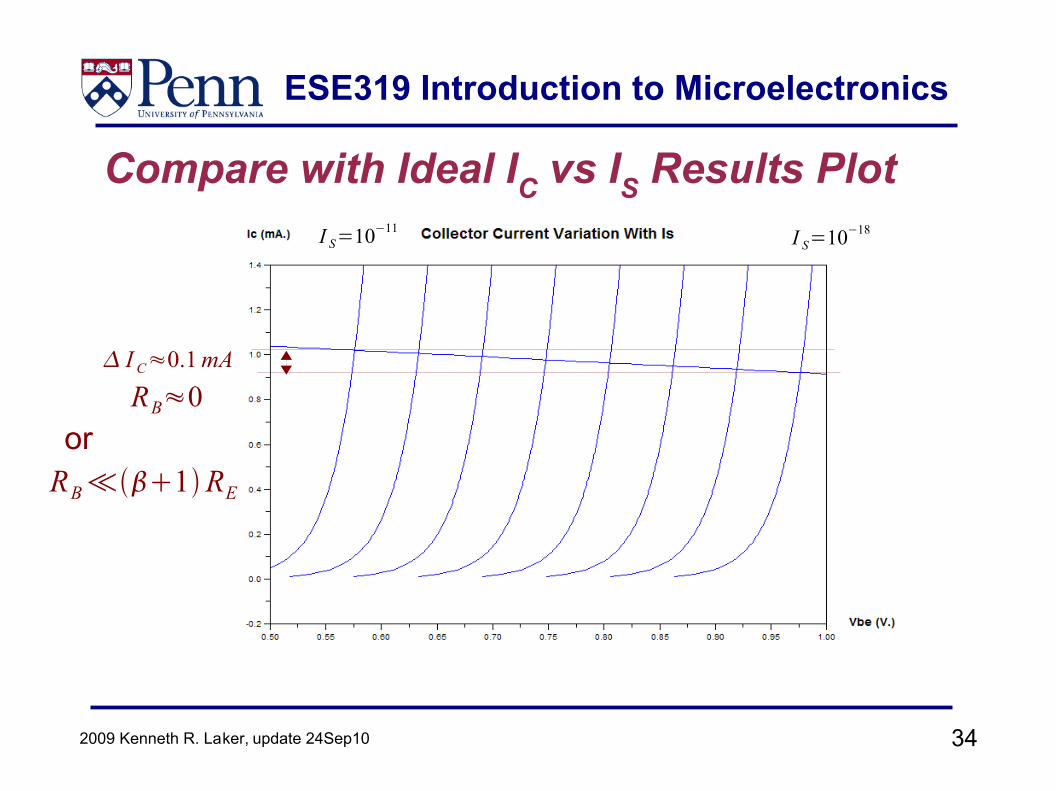
IC vs IS Results PlotI S=10−11 I S=10−18
I C≈0.1 mA Insensitive to I
S!
I C=V B−V BE
RE
I C= I S eV BE
V T
ESE319 Introduction to Microelectronics
92009 Kenneth R. Laker, update 24Sep10
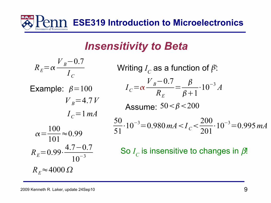
RE=V B−0.7
I C
Example: =100V B=4.7VI C=1mA
RE=0.99⋅4.7−0.710−3
=100101
≈0.99
IC=V B−0.7
RE=
1
⋅10−3 A
Writing IC as a function of β:
Assume: 50200
5051⋅10−3=0.980mAI C
200201
⋅10−3=0.995mA
So IC is insensitive to changes in β!
RE≈4000
Insensitivity to Beta
ESE319 Introduction to Microelectronics
102009 Kenneth R. Laker, update 24Sep10
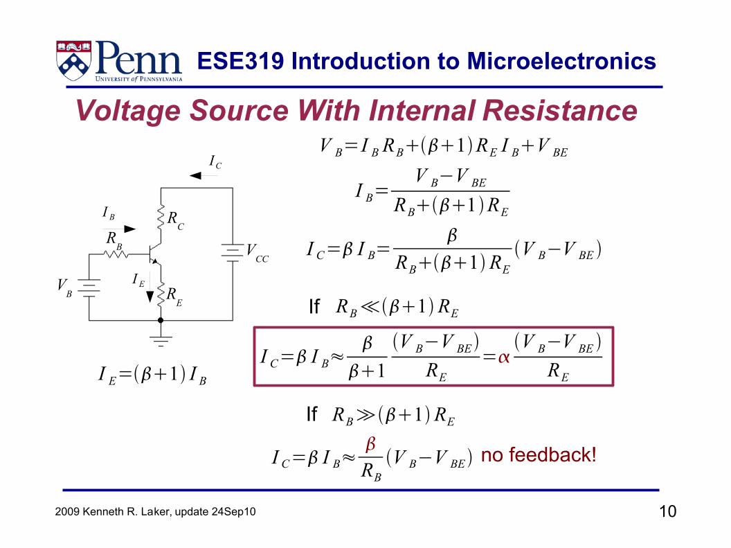
Voltage Source With Internal Resistance
I B
IC
V B=I B RB1RE I BV BE
I B=V B−V BE
RB1RE
I E=1 I B
I C= I B=
RB1REV B−V BE
I C= I B≈
1V B−V BE
RE=
V B−V BE RE
If RB≪1RE
I E
RC
RE
RB
VB
VCC
If RB≫1RE
I C= I B≈RB
V B−V BE no feedback!
ESE319 Introduction to Microelectronics
112009 Kenneth R. Laker, update 24Sep10
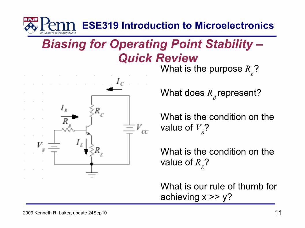
Biasing for Operating Point Stability – Quick Review
What is the purpose RE?
What does RB represent?
What is the condition on the value of V
B?
What is the condition on the value of R
E?
What is our rule of thumb for achieving x >> y?
ESE319 Introduction to Microelectronics
122009 Kenneth R. Laker, update 24Sep10
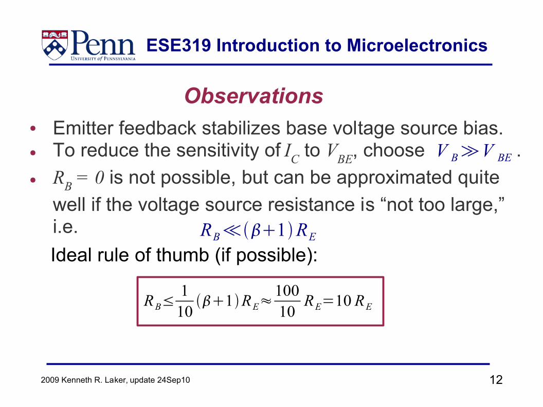
Observations● Emitter feedback stabilizes base voltage source bias.● To reduce the sensitivity of IC to VBE, choose .● RB = 0 is not possible, but can be approximated quite
well if the voltage source resistance is “not too large,” i.e. RB≪1RE
Ideal rule of thumb (if possible):
RB≤1
101RE≈
10010
RE=10 RE
V B≫V BE
ESE319 Introduction to Microelectronics
132009 Kenneth R. Laker, update 24Sep10
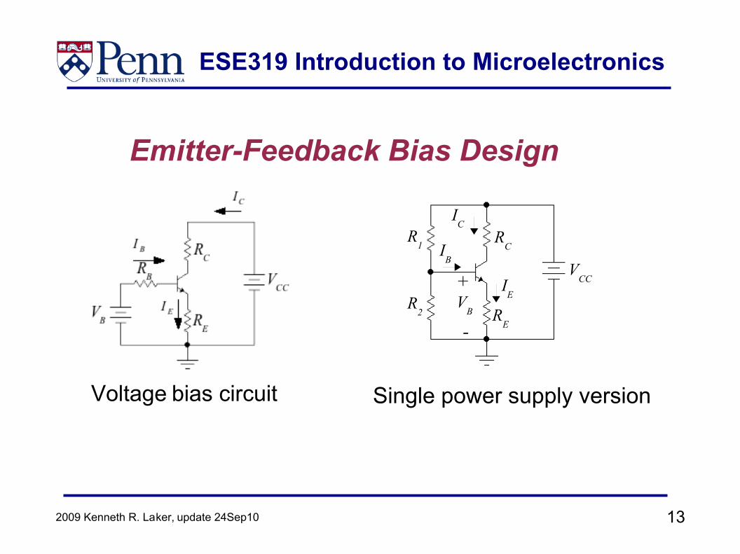
Emitter-Feedback Bias Design
Voltage bias circuit Single power supply version
R1
R2
VCC
RC
RE
IC
IE
IB
VB
+
-
ESE319 Introduction to Microelectronics
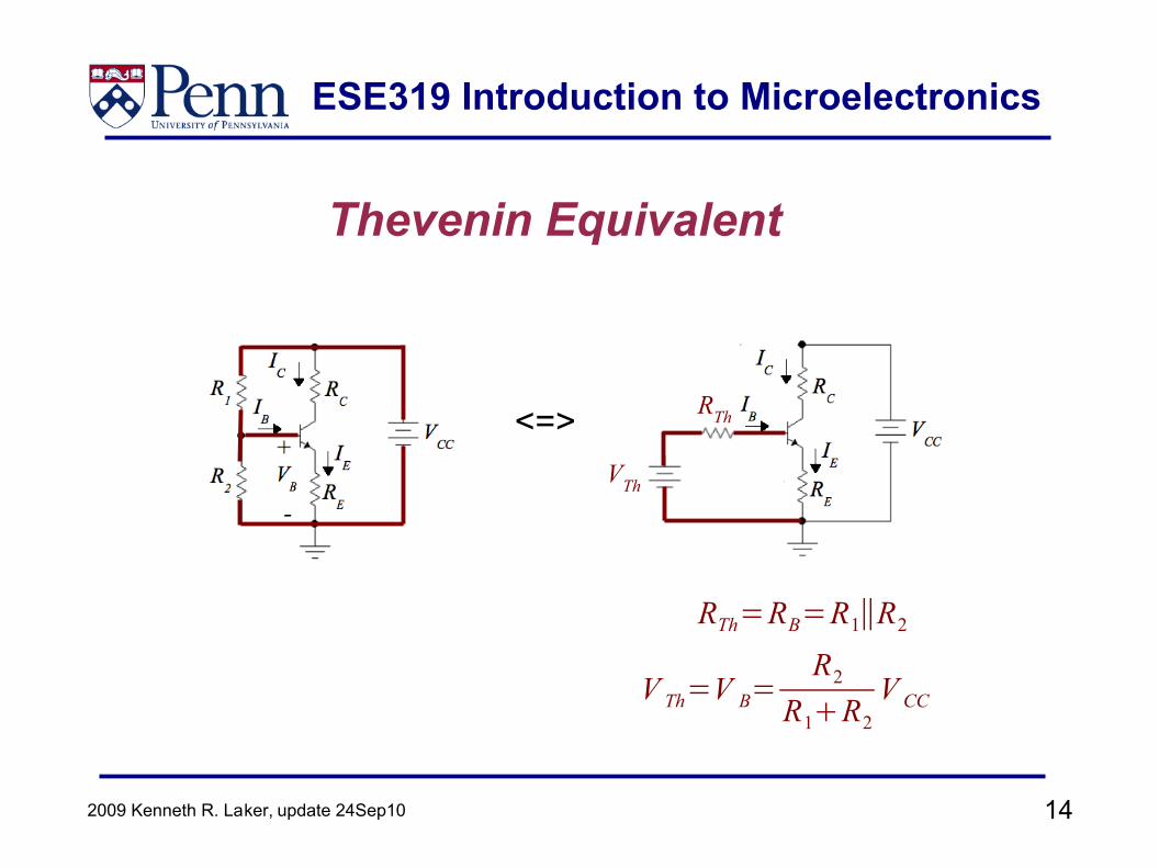
142009 Kenneth R. Laker, update 24Sep10
RTh=RB=R1∥R2
RTh
VTh
V Th=V B=R2
R1R2V CC
<=>
Thevenin Equivalent
ESE319 Introduction to Microelectronics
152009 Kenneth R. Laker, update 24Sep10
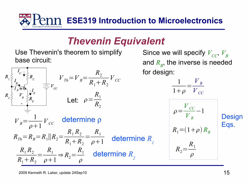
Thevenin EquivalentUse Thevenin's theorem to simplify base circuit:
RTh=RB=R1∥R2=R1 R2
R1R2=
R1
1
Since we will specify VCC, VB and RB, the inverse is needed for design:
11
=V B
V CC
=R1
R2=
V CC
V B−1
R1=1RB
V B=1
1V CC
Let:
R2=R1
Design Eqs.
I B≈0
V Th=V B=R2
R1R2V CC
determine ρ
determine R1
R1 R2
R1R2=
R1
1⇒ R2=
R1
determine R
2
ESE319 Introduction to Microelectronics
162009 Kenneth R. Laker, update 24Sep10
A “Rule of Thumb” for Single Supply Biasing1. Choose RT = R
1 + R
2 so that I1 << IC, i.e.
I1 is about 1/10 of the desired collector (or emitter) current (ignoring I
B):
RT=R1R2=10V CC
I C
2. Use a voltage divider to give the desiredbase voltage V
B and solve for R
2:
R2=RTV B
V CC
R1=RT−R2=RT 1−V B
V CC
I 1
I 1=V CC
RT=
I C
10V
B
+
-
V B=V CC
R2
RT
I 1=V CC
R1R2=
V CC
RT3. Solve for R
1:
I B≈0R1
R2
RC
RE
V CC
I C
4. Calculate RB: RB=R1∥R2
Oops! Ignored I1
in previous slide.
ESE319 Introduction to Microelectronics
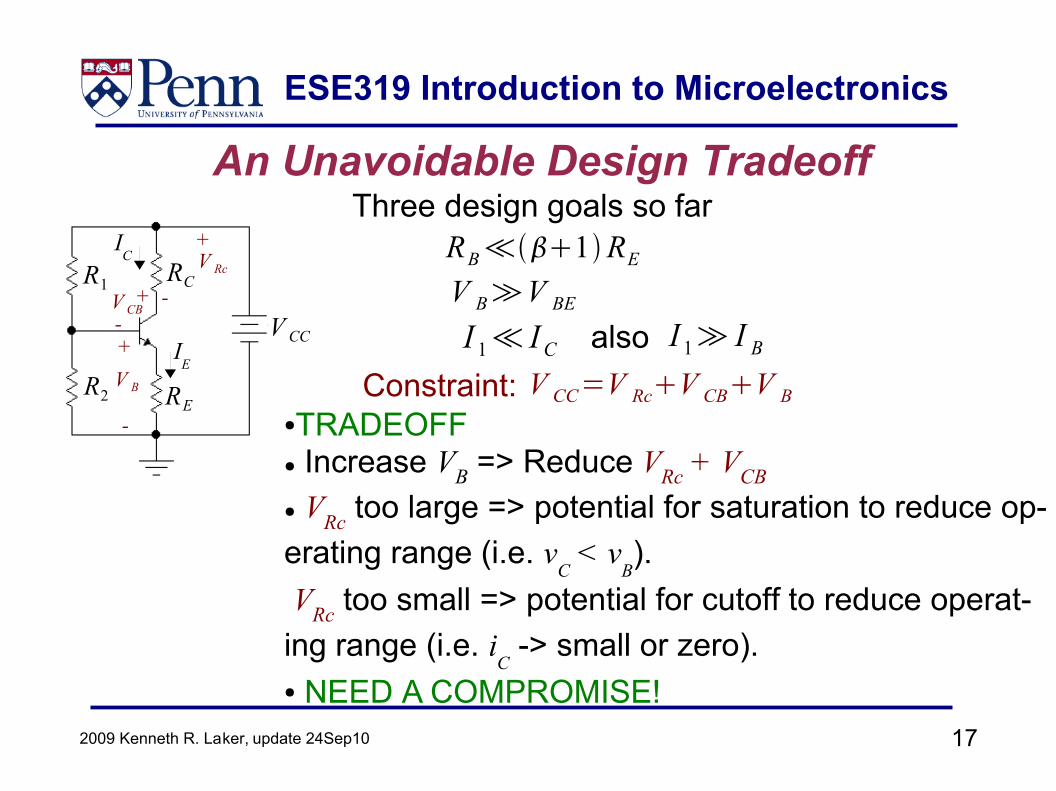
172009 Kenneth R. Laker, update 24Sep10
IC
R1
R2
RC
RE
V CCI
E
V CB+
-
V B
+
-
+
-
V Rc
Three design goals so farRB≪1RE
V B≫V BE
Constraint: V CC=V RcV CBV B●TRADEOFF● Increase VB => Reduce VRc + VCB ● VRc too large => potential for saturation to reduce op-erating range (i.e. v
C < v
B).
VRc too small => potential for cutoff to reduce operat-ing range (i.e. i
C -> small or zero).
● NEED A COMPROMISE!
An Unavoidable Design Tradeoff
I 1≪ I C also I 1≫ I B
ESE319 Introduction to Microelectronics
182009 Kenneth R. Laker, update 24Sep10
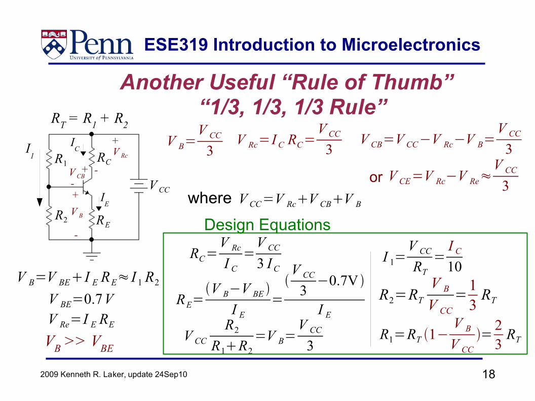
Another Useful “Rule of Thumb” “1/3, 1/3, 1/3 Rule”
V B=V CC
3V Rc=I C RC=
V CC
3V CB=V CC−V Rc−V B=
V CC
3
V CC=V RcV CBV B
RC=V Rc
I C=
V CC
3 I C
RE=V B−V BE
I E=V CC
3−0.7V
I E
V CCR2
R1R2=V B=
V CC
3
Design Equationswhere
IC
R1
R2
RC
RE
V CCI
E
V CB+
-
V B
+
-
+
-
V Rc
V B=V BEI E RE≈ I 1 R2
V BE=0.7V
VB >> VBE
V CE=V Rc−V Re≈V CC
3
V Re=I E RE
or
I 1=V CC
RT=
I C
10
R2=RTV B
V CC=1
3RT
R1=RT 1−V B
V CC=
23
RT
RT = R1 + R2
I1
ESE319 Introduction to Microelectronics
192009 Kenneth R. Laker, update 24Sep10
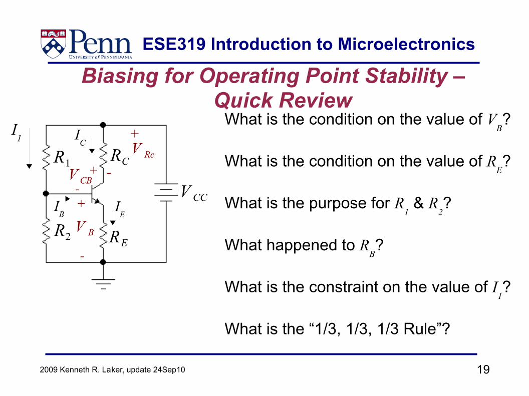
Biasing for Operating Point Stability – Quick Review
What is the condition on the value of VB?
What is the condition on the value of RE?
What is the purpose for R1 & R
2?
What happened to RB?
What is the constraint on the value of I1?
What is the “1/3, 1/3, 1/3 Rule”?
IC
R1
R2
RC
RE
V CCI
E
V CB+
-
V B
+
-
+
-V Rc
I1
IB
ESE319 Introduction to Microelectronics
202009 Kenneth R. Laker, update 24Sep10
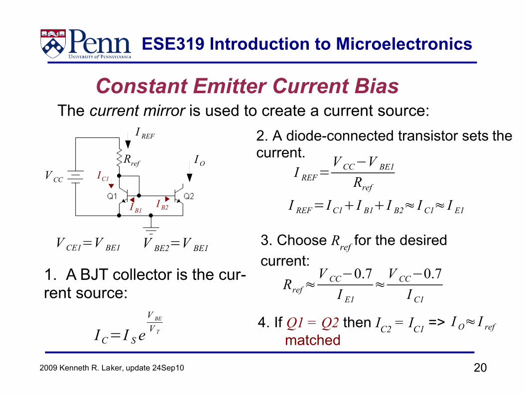
Constant Emitter Current BiasThe current mirror is used to create a current source:
1. A BJT collector is the cur-rent source:
I C=I S eV BE
V T
I REF
I
2. A diode-connected transistor sets the current.
3. Choose Rref for the desiredcurrent:
Rref≈V CC−0.7
I E1≈
V CC−0.7I C1
V BE2=V BE1
I O
I REF=I C1I B1I B2≈ I C1≈ I E1
I REF=V CC−V BE1
Rref
Rref
V CC IC1
I B1I B2
V CE1=V BE1
4. If Q1 = Q2 then IC2 = IC1 => I O≈ I ref
matched
ESE319 Introduction to Microelectronics
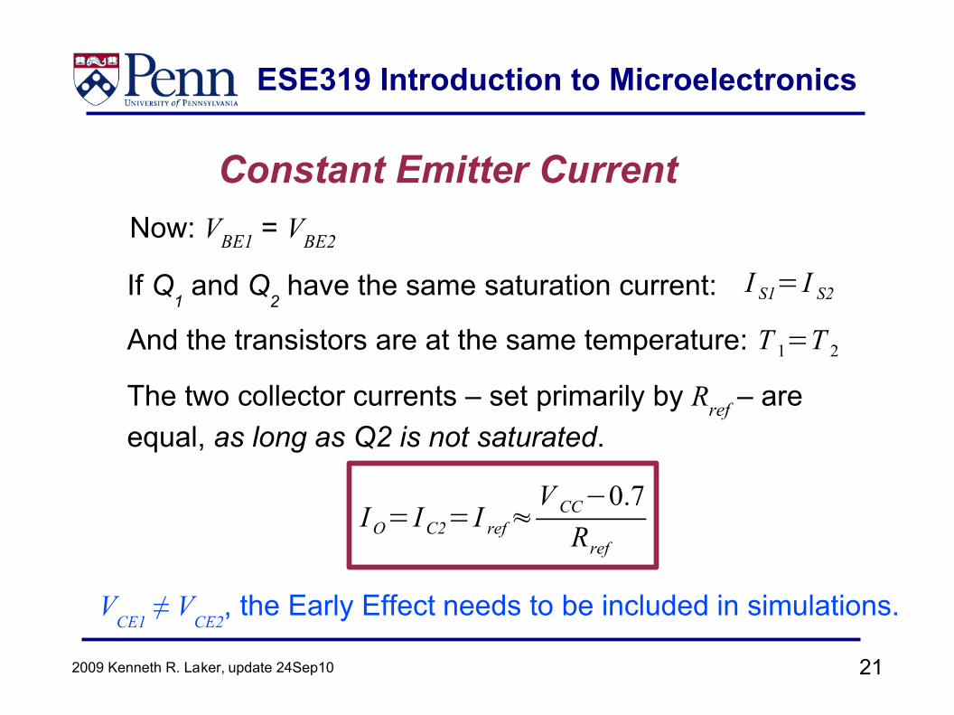
212009 Kenneth R. Laker, update 24Sep10
Constant Emitter Current
If Q1 and Q
2 have the same saturation current:
Now: VBE1 = VBE2
I S1= I S2
And the transistors are at the same temperature: T 1=T 2
The two collector currents – set primarily by Rref – are equal, as long as Q2 is not saturated.
I O= I C2= I ref≈V CC−0.7
Rref
VCE1
≠ VCE2
, the Early Effect needs to be included in simulations.
ESE319 Introduction to Microelectronics
222009 Kenneth R. Laker, update 24Sep10
Constant Emitter Current – Early Voltage
IC2=I O
I B2
I B1
IC1
Assume Q1 = Q2
I O= I C2= I S eV BE /V T 1V CE2
V A
Early Effect
Since IB is not effected by VA, i.e.
I B2=I S
eV BE /V T=
I C2
F
For Q2:
For Q1: IB1
= IB2
I ref= I C1 I B1 I B2= I C12 I B
V BE2=V BE1=V CE1=V BE
I ref= I S eV BE /V T 1V CE1
V A2
I S
e
V BE
V T
F=1V CE2
V Awhere
I S eV BE/V T 1V BE
V A2
I S
e
V BE
V T=
Solving for I S eV BE /V T
I S eV BE/V T=I ref
1V BE
V T 2
I O= I C2= I ref
1V CE2
V A
1V BE
V A 2
(1) (2)
Sub (2) into (1)
RrefI ref
V CC
ESE319 Introduction to Microelectronics
232009 Kenneth R. Laker, update 24Sep10
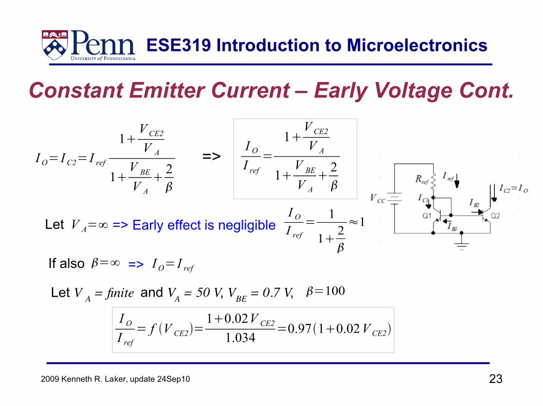
Constant Emitter Current – Early Voltage Cont.
I O= I C2= I ref
1V CE2
V A
1V BE
V A 2
=>I O
I ref=
1V CE2
V A
1V BE
V A 2
Let V A=∞ => Early effect is negligibleI O
I ref=
1
1 2
≈1
I O= I ref=>
Let V A = finite and VA = 50 V, VBE = 0.7 V, =100
I O
I ref= f V CE2=
10.02V CE2
1.034=0.9710.02V CE2
If also =∞
ESE319 Introduction to Microelectronics
242009 Kenneth R. Laker, update 24Sep10
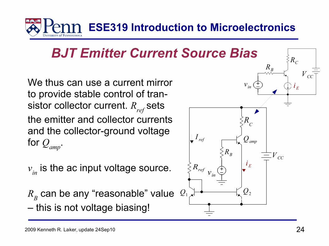
We thus can use a current mirror to provide stable control of tran-sistor collector current. Rref sets the emitter and collector currents and the collector-ground voltage for Qamp.
vin is the ac input voltage source.
RB can be any “reasonable” value – this is not voltage biasing!
Rref
Rref
RB
V B
V CC
vin
I ref
i E
Qamp
Q1Q2
iEv in
V CC
RB
RCBJT Emitter Current Source Bias
RC
ESE319 Introduction to Microelectronics
252009 Kenneth R. Laker, update 24Sep10
Summary● Two practical methods for achieving stable
bias for a BJT are:● Use a voltage source in the base with a feed-
back resistance in the emitter circuit.● Place a current source directly in the emitter cir-
cuit.
ESE319 Introduction to Microelectronics
262009 Kenneth R. Laker, update 24Sep10
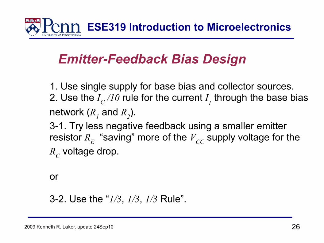
Emitter-Feedback Bias Design
1. Use single supply for base bias and collector sources.2. Use the IC /10 rule for the current I
1 through the base bias
network (R1 and R2).3-1. Try less negative feedback using a smaller emitterresistor RE “saving” more of the VCC supply voltage for theRC voltage drop.
or
3-2. Use the “1/3, 1/3, 1/3 Rule”.
ESE319 Introduction to Microelectronics
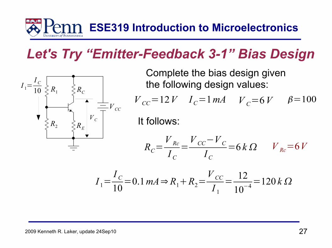
272009 Kenneth R. Laker, update 24Sep10
I 1=I C
10
Let's Try “Emitter-Feedback 3-1” Bias Design
V CC=12V
Complete the bias design giventhe following design values:
I C=1mA V C=6V
It follows:
RC=V Rc
I C=
V CC−V C
I C=6 k
I 1=I C
10=0.1 mA⇒R1R2=
V CC
I 1= 12
10−4=120 k
V C
=100RC
RE
R1
R2
V CC
V Rc=6V
ESE319 Introduction to Microelectronics
282009 Kenneth R. Laker, update 24Sep10
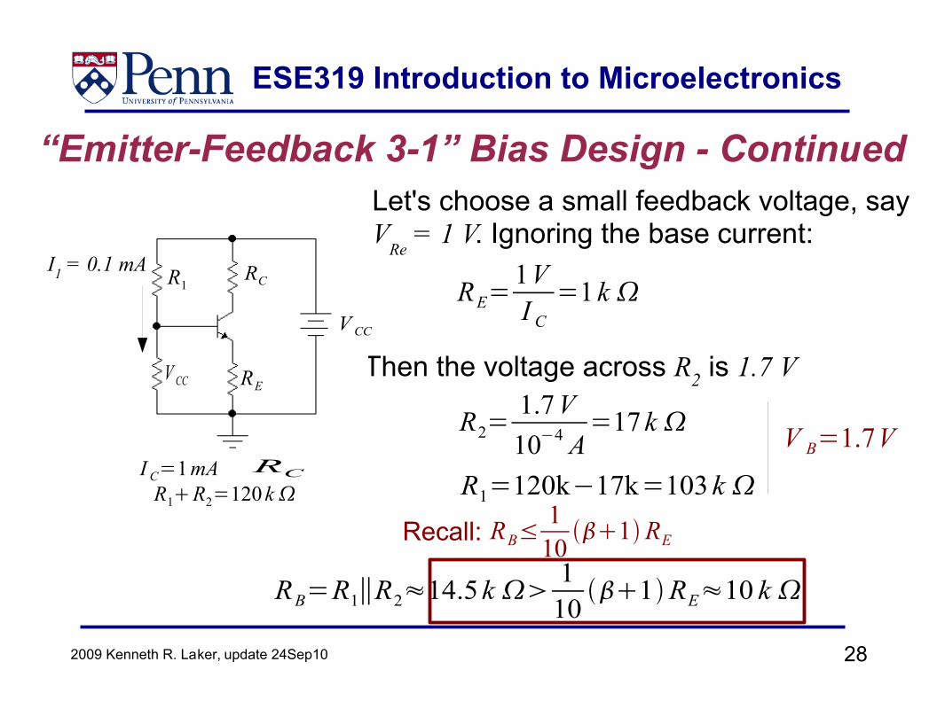
“Emitter-Feedback 3-1” Bias Design - ContinuedLet's choose a small feedback voltage, say V
Re = 1 V. Ignoring the base current:
RE=1VI C
=1k
Then the voltage across R2 is 1.7 V
R2=1.7V10−4 A
=17 k
R1=120k−17k=103 k
RB=R1∥R2≈14.5k 1
101RE≈10 k
I1 = 0.1 mA
I C=1 mAR1R2=120 k
RC
R1
V CC RE
RB≤1
101RERecall:
V B=1.7V
RC
V CC
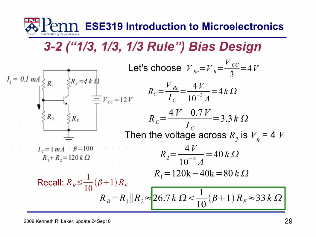
ESE319 Introduction to Microelectronics
292009 Kenneth R. Laker, update 24Sep10
3-2 (“1/3, 1/3, 1/3 Rule”) Bias DesignV Rc=V B=
V CC
3=4V
RC=V Rc
I C= 4V
10−3 A=4 k
RE=4 V−0.7V
I C=3.3k
Then the voltage across R2 is VB = 4 V
R2=4V
10−4 A=40 k
4
Let's choose
R1=120k−40k=80 kRB≤
110
1RERecall:
RB=R1∥R2≈26.7k 1
101RE≈33 k
ESE319 Introduction to Microelectronics
302009 Kenneth R. Laker, update 24Sep10
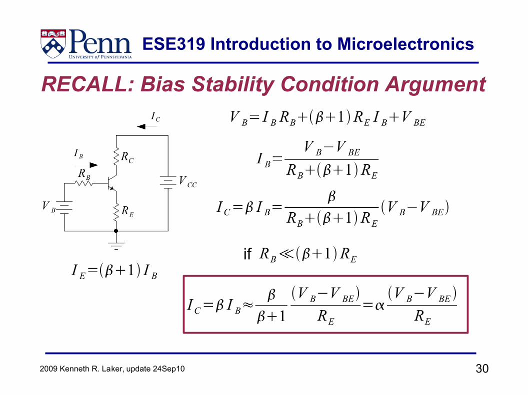
RECALL: Bias Stability Condition Argument
I B
IC V B= I B RB1RE I BV BE
I B=V B−V BE
RB1RE
I E=1 I B
I C= I B=
RB1REV B−V BE
I C= I B≈
1V B−V BE
RE=
V B−V BE RE
RB≪1REif
RC
RE
RB
V B
V CC
ESE319 Introduction to Microelectronics
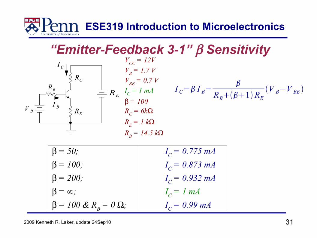
312009 Kenneth R. Laker, update 24Sep10
I C= I B=
RB1REV B−V BE
RC
RE
RB
V B
RE
I C
I B
VCC = 12VVB = 1.7 VVBE = 0.7 VIC = 1 mAβ = 100RC = 6kΩRE = 1 kΩRB = 14.5 kΩ
β = 50; IC = 0.775 mAβ = 100; IC = 0.873 mAβ = 200; IC = 0.932 mAβ = ∞; IC = 1 mAβ = 100 & RB = 0 Ω; IC = 0.99 mA
“Emitter-Feedback 3-1” β Sensitivity
ESE319 Introduction to Microelectronics
322009 Kenneth R. Laker, update 24Sep10
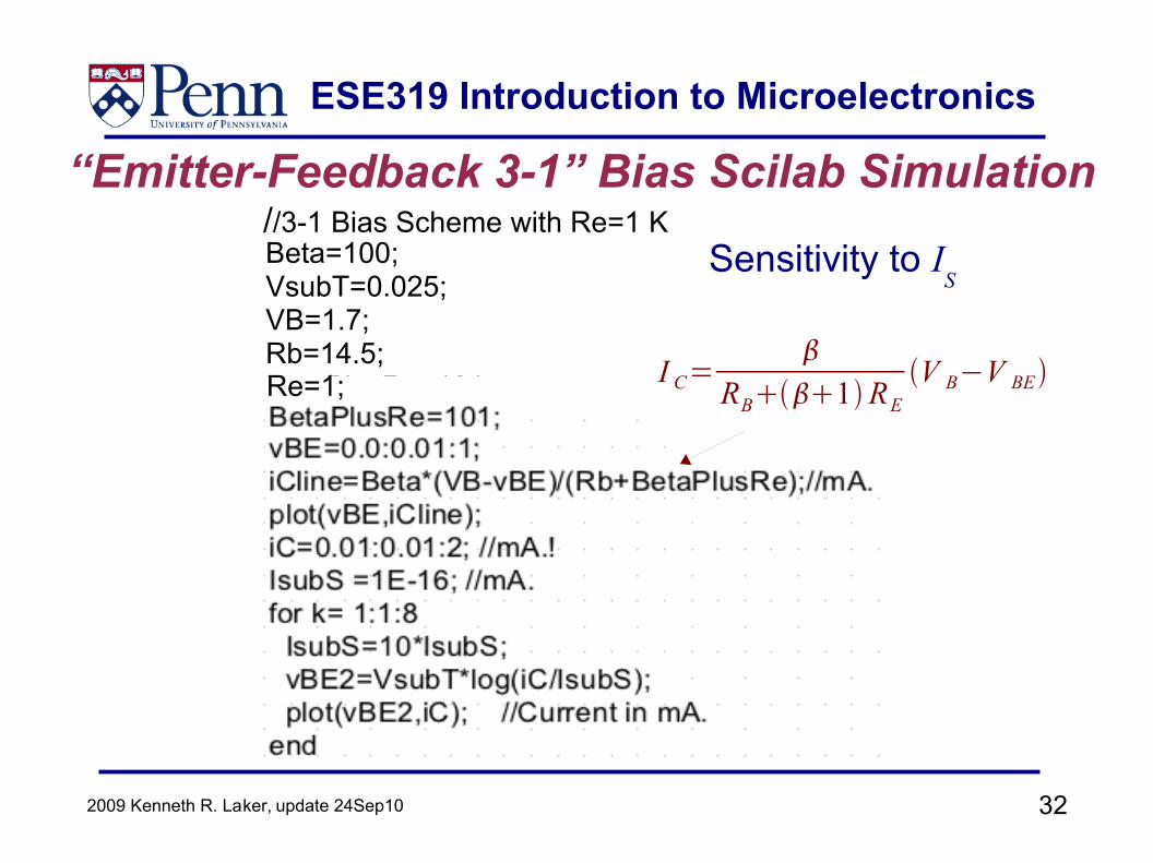
“Emitter-Feedback 3-1” Bias Scilab Simulation//Rule of thumb BJT bias sensitivityBeta=100;VsubT=0.025;VB=1.7;Rb=14.5;BetaPlusRe=101;vBE=0.0:0.01:1;iCline=Beta*(VB-vBE)/(Rb+BetaPlusRe);//mA.plot(vBE,iCline);iC=0.01:0.01:2; //mA.!IsubS =1E-16; //mA.for k= 1:1:8 IsubS=10*IsubS; vBE2=VsubT*log(iC/IsubS); plot(vBE2,iC); //Current in mA.end
Sensitivity to IS
//3-1 Bias Scheme with Re=1 K
Re=1; I C=
RB1REV B−V BE
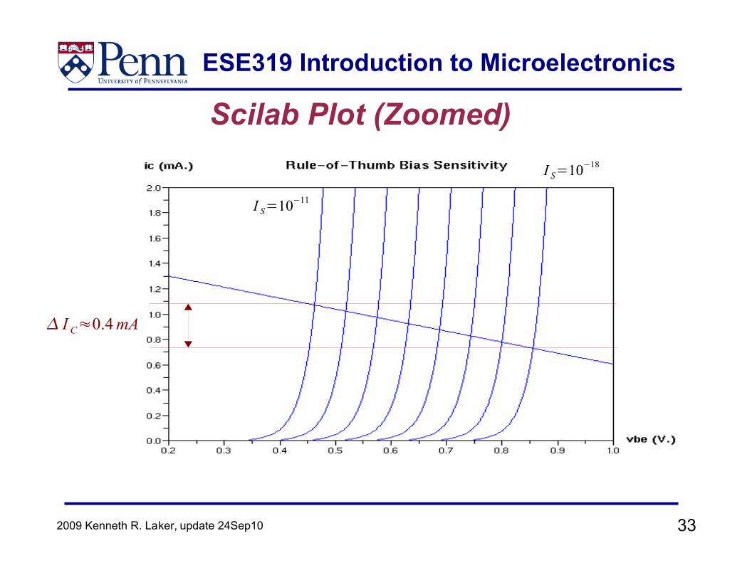
ESE319 Introduction to Microelectronics
332009 Kenneth R. Laker, update 24Sep10
Scilab Plot (Zoomed)
I S=10−11
I S=10−18
I C≈0.4 mA
ESE319 Introduction to Microelectronics
342009 Kenneth R. Laker, update 24Sep10
Compare with Ideal IC vs IS Results PlotI S=10−11 I S=10−18
I C≈0.1 mA
RB≈0or
RB≪1RE
ESE319 Introduction to Microelectronics
352009 Kenneth R. Laker, update 24Sep10
Conclusion
“1/3, 1/3, 1/3 Rule” Provides a Good Compromise Base Voltage Bias Scheme
![Chapter 5 BJT Biasing Circuits Engineering/833... · 2017. 12. 8. · BJT Biasing Circuits 5.1 The DC Operation Point [5] DC Bias: Bias establishes the dc operating point for proper](https://img.pdfslide.us/doc/110x75/6109b3612d57d967952ea81a/chapter-5-bjt-biasing-circuits-engineering833-2017-12-8-bjt-biasing-circuits.jpg)