Embed Size (px)
Citation preview
1
Chapter 2. - DC Biasing - BJTs
Objectives
To Understand :• Concept of Operating point and stability• Analyzing Various biasing circuits and their comparison with respect to stability
BJT – A Review
• Invented in 1948 by Bardeen, Brattain and Shockley• Contains three adjoining, alternately doped semiconductor regions: Emitter (E),
Base (B), and Collector (C)• The middle region, base, is very thin• Emitter is heavily doped compared to collector. So, emitter and collector are not
interchangeable.
Three operating regions
• Linear – region operation:– Base – emitter junction forward biased– Base – collector junction reverse biased
• Cutoff – region operation:– Base – emitter junction reverse biased– Base – collector junction reverse biased
• Saturation – region operation:– Base – emitter junction forward biased– Base – collector junction forward biased
Three operating regions of BJT
• Cut off: VCE = VCC, IC 0
• Active or linear : VCE VCC/2 , IC IC max/2
• Saturation: VCE 0 , IC IC max
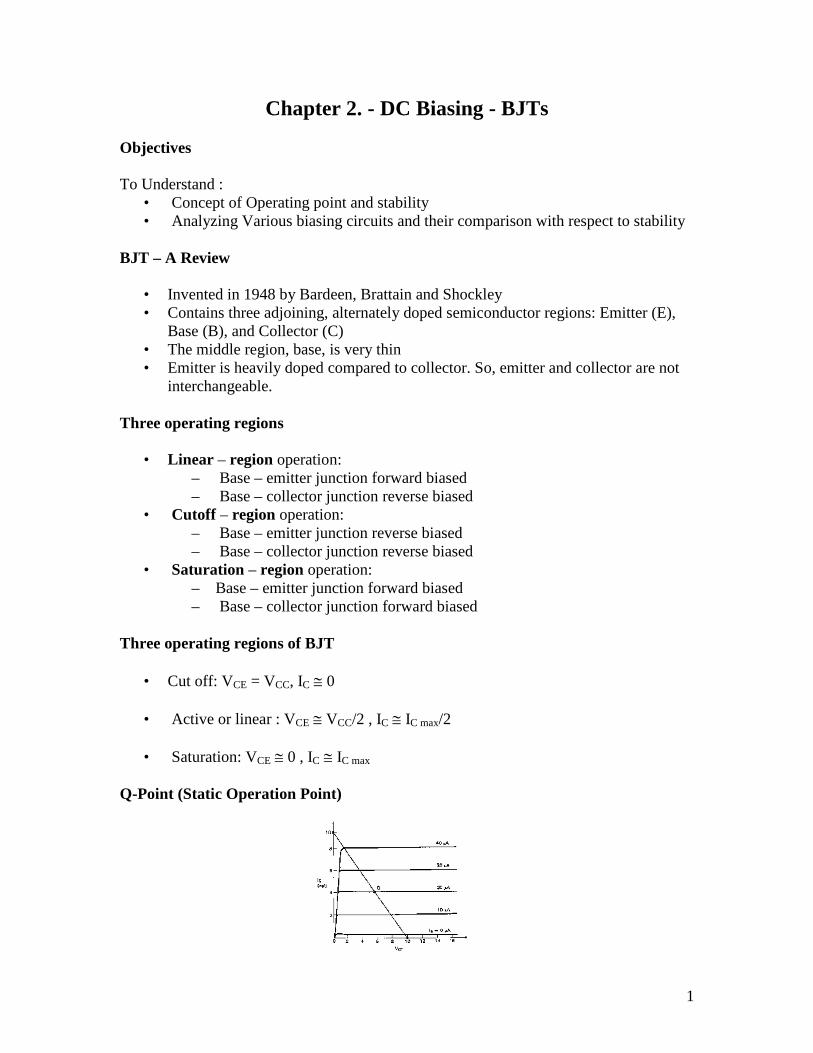
Q-Point (Static Operation Point)

2
• The values of the parameters IB, IC and VCE together are termed as ‘operatingpoint’ or Q ( Quiescent) point of the transistor.
Q-Point
• The intersection of the dc bias value of IB with the dc load line determines the Q-point.
• It is desirable to have the Q-point centered on the load line. Why?• When a circuit is designed to have a centered Q-point, the amplifier is said to be
midpoint biased.• Midpoint biasing allows optimum ac operation of the amplifier.
Introduction - Biasing
The analysis or design of a transistor amplifier requires knowledge of both the dc andac response of the system.In fact, the amplifier increases the strength of a weak signalby transferring the energy from the applied DC source to the weak input ac signal• The analysis or design of any electronic amplifier therefore has two components:
• The dc portion and• The ac portion
During the design stage, the choice of parameters for the required dc levels willaffect the ac response.
What is biasing circuit?
• Once the desired dc current and voltage levels have been identified, a networkmust be constructed that will establish the desired values of IB, IC and VCE, Such anetwork is known as biasing circuit. A biasing network has to preferably makeuse of one power supply to bias both the junctions of the transistor.
Purpose of the DC biasing circuit
• To turn the device “ON”• To place it in operation in the region of its characteristic where the device
operates most linearly, i.e. to set up the initial dc values of IB, IC, and VCE
Important basic relationship
• VBE = 0.7V• IE = ( + 1) IB IC
• IC = IB
3
Biasing circuits:
• Fixed – bias circuit• Emitter bias• Voltage divider bias• DC bias with voltage feedback• Miscellaneous bias
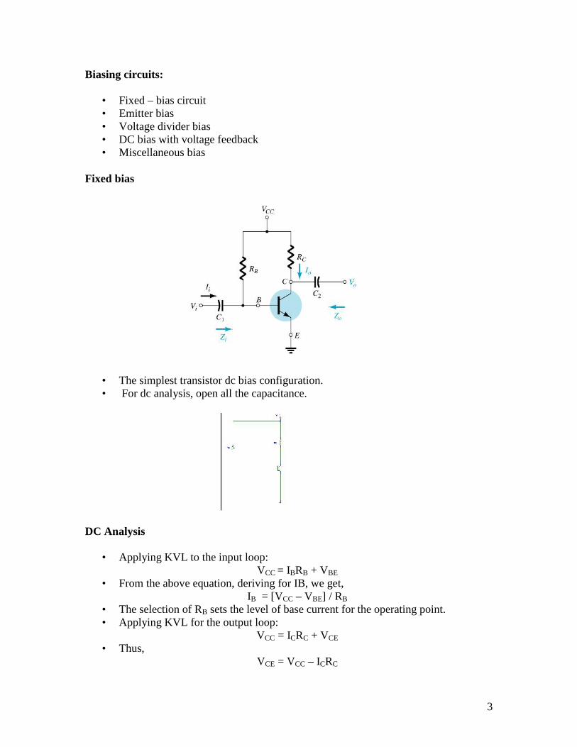
Fixed bias
• The simplest transistor dc bias configuration.• For dc analysis, open all the capacitance.
DC Analysis
• Applying KVL to the input loop:VCC = IBRB + VBE
• From the above equation, deriving for IB, we get,IB = [VCC – VBE] / RB
• The selection of RB sets the level of base current for the operating point.• Applying KVL for the output loop:
VCC = ICRC + VCE
• Thus,VCE = VCC – ICRC

4
• In circuits where emitter is grounded,VCE = VE
VBE = VB
Design and Analysis
• Design: Given – IB, IC , VCE and VCC, or IC , VCE and , design the values of RB,RC using the equations obtained by applying KVL to input and output loops.
• Analysis: Given the circuit values (VCC, RB and RC), determine the values of IB,IC , VCE using the equations obtained by applying KVL to input and output loops.
Problem – Analysis
Given the fixed bias circuit with VCC = 12V, RB = 240 k, RC = 2.2 k and = 75.Determine the values of operating point.
Equation for the input loop is:IB = [VCC – VBE] / RB where VBE = 0.7V,
thus substituting the other given values in the equation, we get
IB = 47.08uAIC = IB = 3.53mA
VCE = VCC – ICRC = 4.23V• When the transistor is biased such that IB is very high so as to make IC very high
such that ICRC drop is almost VCC and VCE is almost 0, the transistor is said to bein saturation.
IC sat = VCC / RC in a fixed bias circuit.
Verification
• Whenever a fixed bias circuit is analyzed, the value of ICQ obtained could beverified with the value of ICSat ( = VCC / RC) to understand whether the transistor isin active region.
• In active region,ICQ = ( ICSat /2)
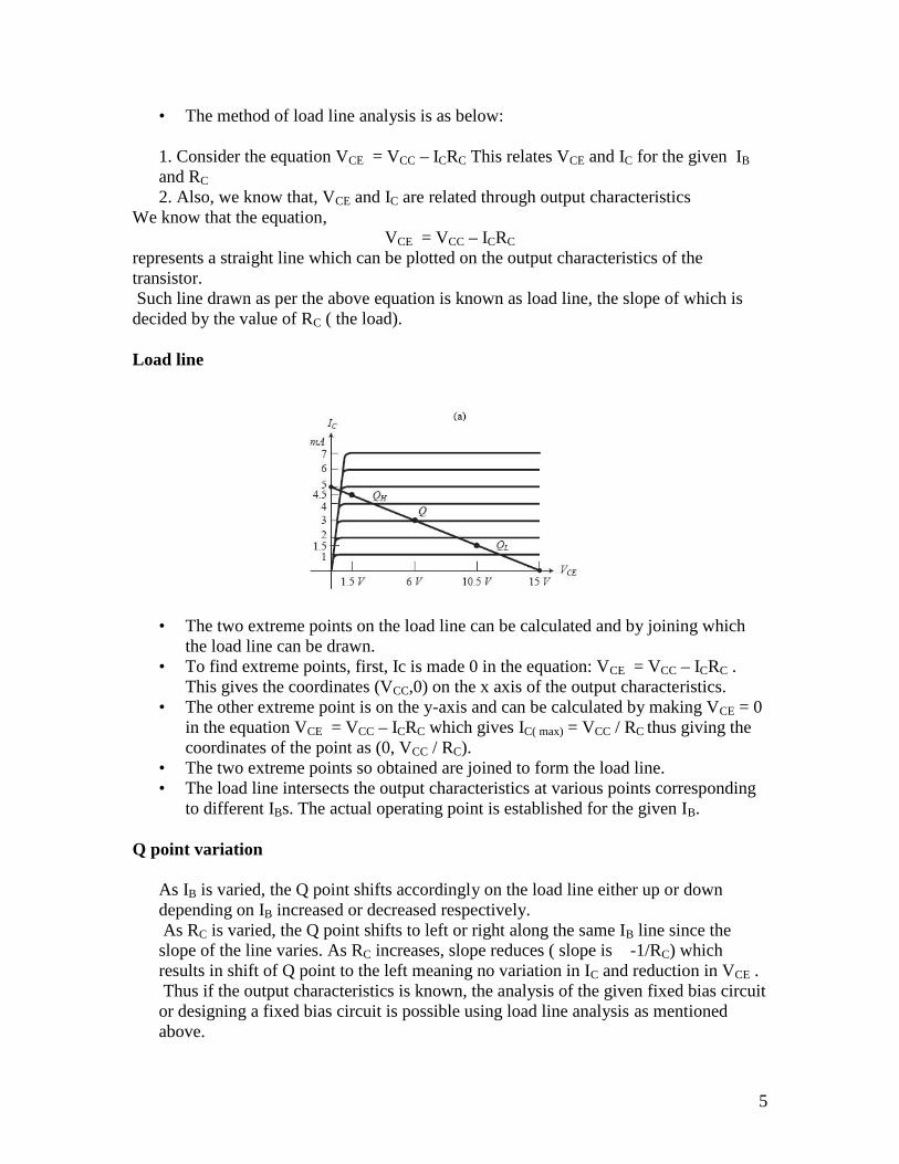
Load line analysis
A fixed bias circuit with given values of VCC, RC and RB can be analyzed ( means,determining the values of IBQ, ICQ and VCEQ) using the concept of load line also.Here the input loop KVL equation is not used for the purpose of analysis, instead, theoutput characteristics of the transistor used in the given circuit and output loop KVLequation are made use of.
5
• The method of load line analysis is as below:
1. Consider the equation VCE = VCC – ICRC This relates VCE and IC for the given IB
and RC
2. Also, we know that, VCE and IC are related through output characteristicsWe know that the equation,
VCE = VCC – ICRC
represents a straight line which can be plotted on the output characteristics of thetransistor.Such line drawn as per the above equation is known as load line, the slope of which is
decided by the value of RC ( the load).
Load line
• The two extreme points on the load line can be calculated and by joining whichthe load line can be drawn.
• To find extreme points, first, Ic is made 0 in the equation: VCE = VCC – ICRC .This gives the coordinates (VCC,0) on the x axis of the output characteristics.
• The other extreme point is on the y-axis and can be calculated by making VCE = 0in the equation VCE = VCC – ICRC which gives IC( max) = VCC / RC thus giving thecoordinates of the point as (0, VCC / RC).
• The two extreme points so obtained are joined to form the load line.• The load line intersects the output characteristics at various points corresponding
to different IBs. The actual operating point is established for the given IB.
Q point variation
As IB is varied, the Q point shifts accordingly on the load line either up or downdepending on IB increased or decreased respectively.As RC is varied, the Q point shifts to left or right along the same IB line since the
slope of the line varies. As RC increases, slope reduces ( slope is -1/RC) whichresults in shift of Q point to the left meaning no variation in IC and reduction in VCE .Thus if the output characteristics is known, the analysis of the given fixed bias circuit
or designing a fixed bias circuit is possible using load line analysis as mentionedabove.
6
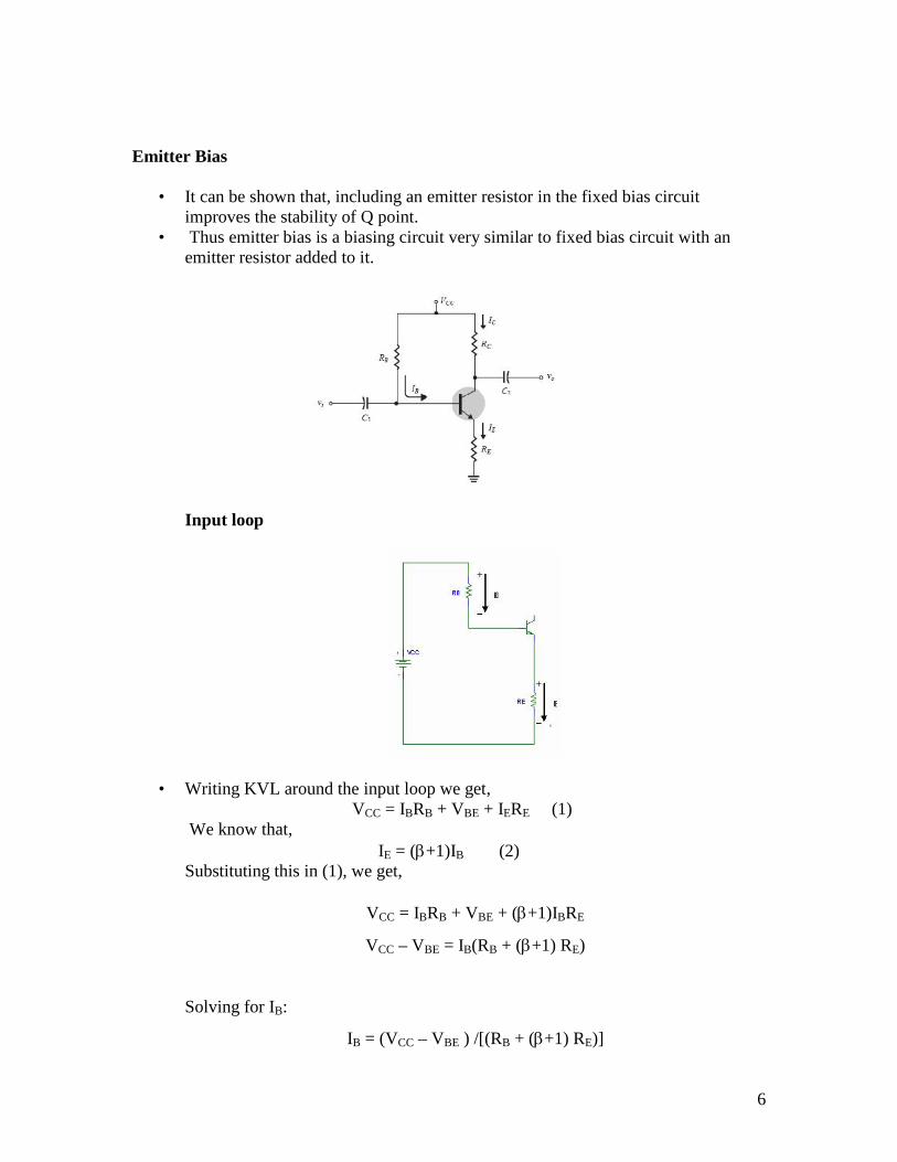
Emitter Bias
• It can be shown that, including an emitter resistor in the fixed bias circuitimproves the stability of Q point.
• Thus emitter bias is a biasing circuit very similar to fixed bias circuit with anemitter resistor added to it.
Input loop
• Writing KVL around the input loop we get,VCC = IBRB + VBE + IERE (1)
We know that,IE = (+1)IB (2)
Substituting this in (1), we get,
VCC = IBRB + VBE + (+1)IBRE
VCC – VBE = IB(RB + (+1) RE)
Solving for IB:
IB = (VCC – VBE ) /[(RB + (+1) RE)]
7
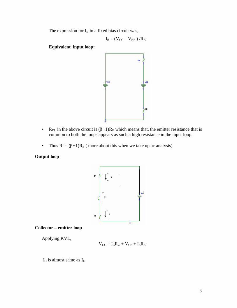
The expression for IB in a fixed bias circuit was,
IB = (VCC – VBE ) /RB
Equivalent input loop:
• REI in the above circuit is (+1)RE which means that, the emitter resistance that iscommon to both the loops appears as such a high resistance in the input loop.
• Thus Ri = (+1)RE ( more about this when we take up ac analysis)
Output loop
Collector – emitter loop
Applying KVL,VCC = ICRC + VCE + IERE
IC is almost same as IE

8
Thus,
VCC = ICRC + VCE + ICRE
= IC (RC + RE) +VCE
VCE = VCC - IC (RC + RE)
Since emitter is not connected directly to ground, it is at a potential VE, given by,
VE = IERE
VC = VCE + VE OR VC = VCC – ICRC
Also, VB = VCC – IBRB OR VB = VBE + VE
Problem:
Analyze the following circuit: given = 75, VCC = 16V, RB = 430k, RC = 2k and RE = 1k
Solution:
IB = (VCC – VBE ) /[(RB + (+1) RE)]
= ( 16 – 0.7) / [ 430k + (76) 1k] = 30.24A
IC = ( 75) (30.24A) = 2.27mA
VCE = VCC - IC (RC + RE) = 9.19V
VC = VCC – ICRC = 11.46V
VE = VC – VCE = 2.27V
VB = VBE + VE = 2.97V
VBC = VB – VC = 2.97 – 11.46 = - 8.49V

9
Improved bias stability
• Addition of emitter resistance makes the dc bias currents and voltages remaincloser to their set value even with variation in
– transistor beta– temperature
Stability
In a fixed bias circuit, IB does not vary with and therefore whenever there is anincrease in , IC increases proportionately, and thus VCE reduces making the Q pointto drift towards saturation.In an emitter bias circuit, As increases, IB reduces,maintaining almost same IC and VCE thus stabilizing the Q point against variations.
Saturation current
In saturation VCE is almost 0V, thus
VCC = IC ( RC + RE )Thus, saturation current
IC,sat = VCC / ( RC + RE )
Load line analysis
The two extreme points on the load line of an emitter bias circuit are,
(0, VCC / [ RC + RE ]) on the Y axis, and
( VCC, 0) on the X axis.
Voltage divider bias
RC
R1
+VCC
RE
R2
v out
v in
C2C1
C3

10
This is the biasing circuit wherein, ICQ and VCEQ are almost independent of .The level of IBQ will change with so as to maintain the values of ICQ and VCEQ almost
same, thus maintaining the stability of Q point.
Two methods of analyzing a voltage divider bias circuit are:Exact method – can be applied to any voltage divider circuitApproximate method – direct method, saves time and energy, can be applied in most ofthe circuits.
Exact method
In this method, the Thevenin equivalent network for the network to the left of the baseterminal to be found.
To find Rth:
From the above circuit,
Rth = R1 R2
= R1 R2 / (R1 + R2)

11
To find Eth
From the above circuit,
Eth = VR2 = R2VCC / (R1 + R2)
In the above network, applying KVL
( Eth – VBE) = IB [ Rth +( + 1) RE ]
IB = ( Eth – VBE) / [ Rth +( + 1) RE ]
Analysis of Output loop
KVL to the output loop:
VCC = ICRC + VCE + IERE
IE IC
Thus, VCE = VCC – IC (RC + RE)
Note that this is similar to emitter bias circuit.

12
Problem
For the circuit given below, find IC and VCE.Given the values of R1, R2, RC, RE and = 140 and VCC = 18V.For the purpose of DC analysis, all the capacitors in the amplifier circuit are opened.
Solution
Considering exact analysis:
1. Let us find Rth = R1 R2
= R1 R2 / (R1 + R2) = 3.55K
2. Then find Eth = VR2 = R2VCC / (R1 + R2)
= 1.64V3. Then find IB
IB = ( Eth – VBE) / [ Rth +( + 1) RE ]
= 4.37A
4. Then find IC = IB = 0.612mA
5. Then find VCE = VCC – IC (RC + RE)= 12.63V
13
Approximate analysis:
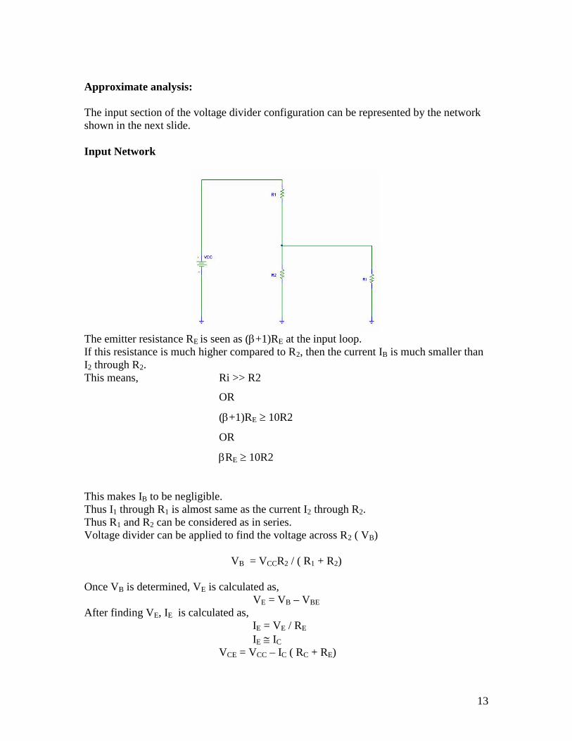
The input section of the voltage divider configuration can be represented by the networkshown in the next slide.
Input Network
The emitter resistance RE is seen as (+1)RE at the input loop.If this resistance is much higher compared to R2, then the current IB is much smaller thanI2 through R2.This means, Ri >> R2
OR
(+1)RE 10R2
OR
RE 10R2
This makes IB to be negligible.Thus I1 through R1 is almost same as the current I2 through R2.Thus R1 and R2 can be considered as in series.Voltage divider can be applied to find the voltage across R2 ( VB)
VB = VCCR2 / ( R1 + R2)
Once VB is determined, VE is calculated as,VE = VB – VBE
After finding VE, IE is calculated as,IE = VE / RE
IE IC
VCE = VCC – IC ( RC + RE)
14
Problem
Given: VCC = 18V, R1 = 39k , R2 = 3.9k , RC = 4k , RE = 1.5k and = 140.Analyse the circuit using approximate technique.In order to check whether approximate technique can be used, we need to verify thecondition,
RE 10R2
Here,RE = 210 k and 10R2 = 39 k
Thus the conditionRE 10R2 satisfied
Solution
• Thus approximate technique can be applied.
1. Find VB = VCCR2 / ( R1 + R2) = 1.64V
2. Find VE = VB – 0.7 = 0.94V
3. Find IE = VE / RE = 0.63mA = IC
4. Find VCE = VCC – IC(RC + RE) = 12.55V
Comparison
Exact Analysis Approximate Analysis
IC = 0.612mA IC = 0.63mA
VCE = 12.63V VCE = 12.55V
Both the methods result in the same values for IC and VCE since the condition RE 10R2 is satisfied.It can be shown that the results due to exact analysis and approximate analysis havemore deviation if the above mentioned condition is not satisfied.For load line analysis of voltage divider network, Ic,max = VCC/ ( RC+RE) when VCE
= 0V and VCE max = VCC when IC = 0.

15
DC bias with voltage feedback
Input loop
Applying KVL for Input Loop:
VCC = IC1RC + IBRB + VBE + IERE
Substituting for IE as ( +1)IB and solving for IB,
IB = ( VCC – VBE) / [ RB + ( RC + RE)]
Output loop

16
Neglecting the base current, KVL to the output loop results in,
VCE = VCC – IC ( RC + RE)
DC bias with voltage feedback
Input loop
Applying KVL to input loop:
VCC = ICRC + IBRB + VBE + IERE
IC IC and IC IE
Substituting for IE as ( +1)IB [ or as IB] and solving for IB,
IB = ( VCC – VBE) / [ RB + ( RC + RE)]
Output loop

17
Neglecting the base current, and applying KVL to the output loop results in,
VCE = VCC – IC ( RC + RE)
In this circuit, improved stability is obtained by introducing a feedback path fromcollector to base.Sensitivity of Q point to changes in beta or temperature variations is normally less thanthat encountered for the fixed bias or emitter biased configurations.
Problem:
Given:VCC = 10V, RC = 4.7k, RB = 250 and RE = 1.2k. = 90.Analyze the circuit.
IB = ( VCC – VBE) / [ RB + ( RC + RE)]
= 11.91A
IC = ( IB ) = 1.07mA
VCE = VCC – IC ( RC + RE) = 3.69V
In the above circuit, Analyze the circuit if = 135 ( 50% increase).
With the same procedure as followed in the previous problem, we get
IB = 8.89A
IC = 1.2mA
VCE = 2.92V
50% increase in resulted in 12.1% increase in IC and 20.9% decrease in VCEQ
Problem 2:

18
Determine the DC level of IB and VC for the network shown:
Solution:
Open all the capacitors for DC analysis.
RB = 91 k + 110 k = 201k
IB = ( VCC – VBE) / [ RB + ( RC + RE)]
= (18 – 0.7) / [ 201k + 75( 3.3+0.51)]
= 35.5A
IC = IB = 2.66mA
VCE = VCC – (ICRC)
= 18 – ( 2.66mA)(3.3k)
= 9.22V
Load line analysis
The two extreme points of the load line IC,max and VCE, max are found in the same as avoltage divider circuit.
IC,max = VCC / (RC + RE) – Saturation current
VCE, max – Cut off voltage
Miscellaneous bias configurations
19
There are a number of BJT bias configurations that do not match the basic types ofbiasing that are discussed till now.
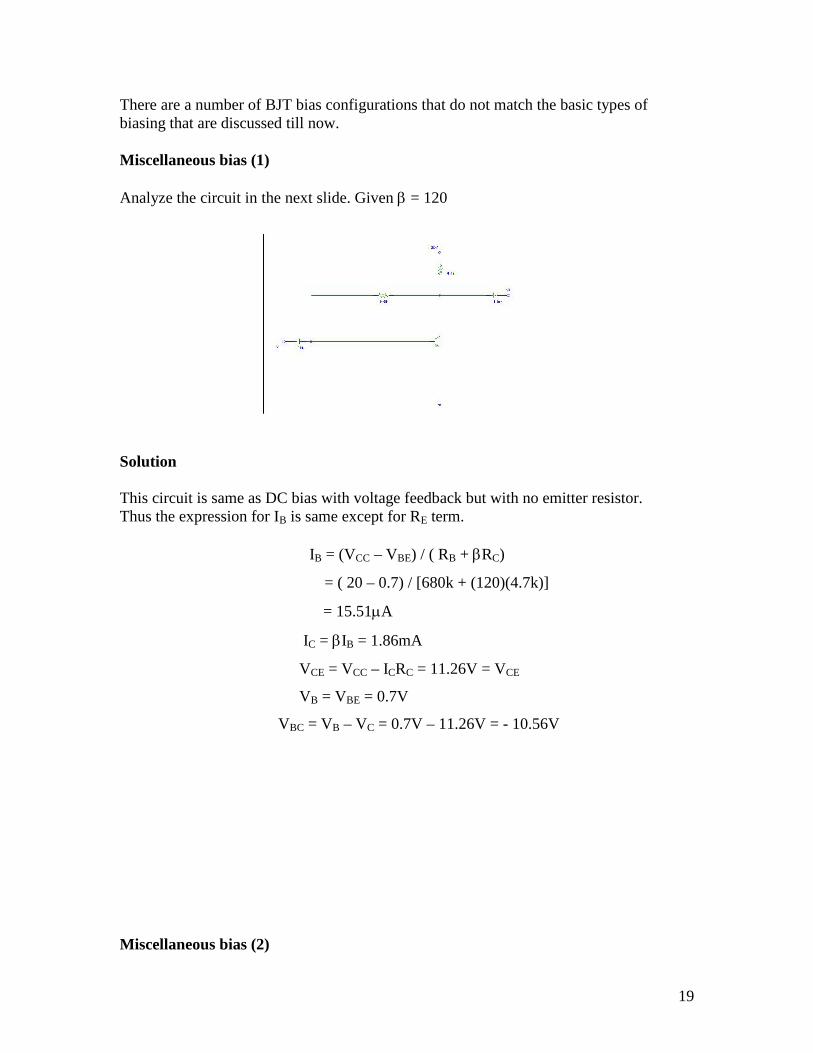
Miscellaneous bias (1)
Analyze the circuit in the next slide. Given = 120
Solution
This circuit is same as DC bias with voltage feedback but with no emitter resistor.Thus the expression for IB is same except for RE term.
IB = (VCC – VBE) / ( RB + RC)
= ( 20 – 0.7) / [680k + (120)(4.7k)]
= 15.51A
IC = IB = 1.86mA
VCE = VCC – ICRC = 11.26V = VCE
VB = VBE = 0.7V
VBC = VB – VC = 0.7V – 11.26V = - 10.56V
Miscellaneous bias (2)

20
Equivalent circuit
Input loop
Output loop

21
Solution
The above circuit is fixed bias circuit.
Applying KVL to input loop:
VEE = VBE + IBRB
IB = ( VEE – VBE) / RB = 83A
IC = IB = 3.735mA
VC = -ICRC = - 4.48V
VB = - IBRB = - 8.3V
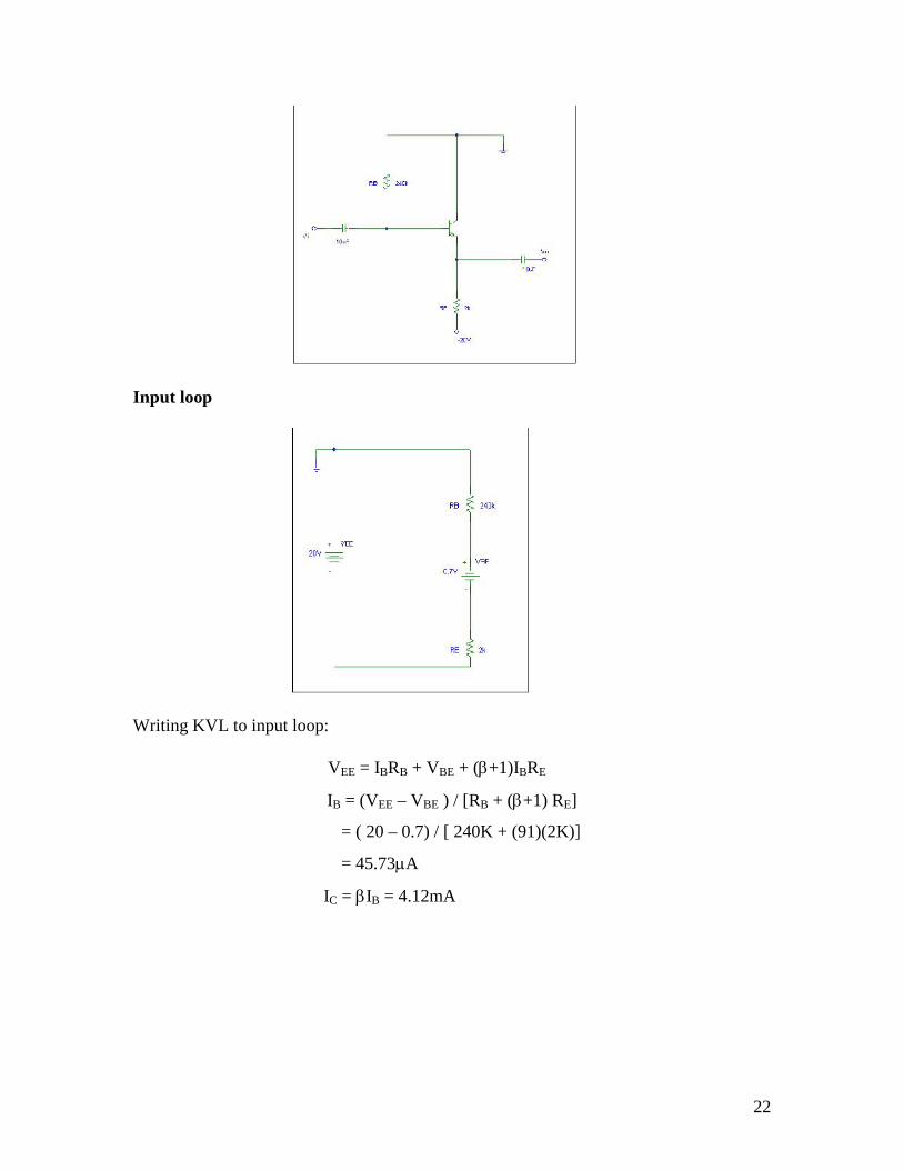
Miscellaneous bias (3)
Determine VCE,Q and IE for the network.Given = 90( Note that the circuit given is common collector mode which can be identified byNo resistance connected to the collector output taken at the emitter)
22
Input loop
Writing KVL to input loop:
VEE = IBRB + VBE + (+1)IBRE
IB = (VEE – VBE ) / [RB + (+1) RE]
= ( 20 – 0.7) / [ 240K + (91)(2K)]
= 45.73A
IC = IB = 4.12mA
23
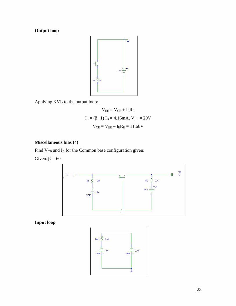
Output loop
Applying KVL to the output loop:
VEE = VCE + IERE
IE = (+1) IB = 4.16mA, VEE = 20V
VCE = VEE – IERE = 11.68V
Miscellaneous bias (4)
Find VCB and IB for the Common base configuration given:
Given: = 60
Input loop

24
Applying KVL to input loop
IE = ( VEE – VBE ) / RE
= 2.75mA
IE = IC = 2.75mA
IB = IC / = 45.8A
Output loop
Applying KVL to output loop:
VCC = ICRC + VCB
VCB = VCC – ICRC = 3.4V
Miscellaneous bias (5)
Determine VC and VB for the network given below.Given = 120Note that this is voltage divider circuit with split supply.( +VCC at the collector and – VEE at the emitter)

25
Thevinin equivalent at the input
Rth= (8.2k)(2.2k) / [ 8.2k+2.2k] = 1.73k
I = (VCC + VEE) / [R1 + R2]
= ( 20 + 20) / ( 8.2K + 2.2K)
= 3.85mA
Eth = IR2 – VEE
= - 11.53V
Equivalent circuit
26
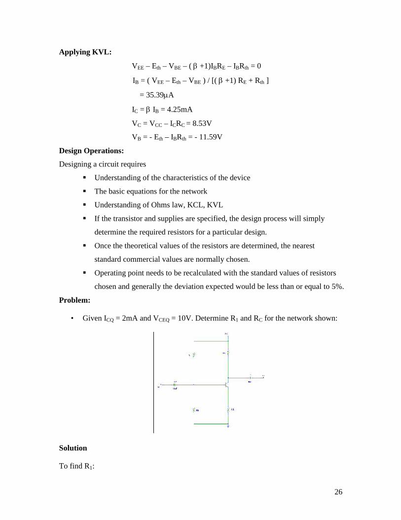
Applying KVL:
VEE – Eth – VBE – ( +1)IBRE – IBRth = 0
IB = ( VEE – Eth – VBE ) / [( +1) RE + Rth ]
= 35.39A
IC = IB = 4.25mA
VC = VCC – ICRC = 8.53V
VB = - Eth – IBRth = - 11.59V
Design Operations:
Designing a circuit requires
Understanding of the characteristics of the device
The basic equations for the network
Understanding of Ohms law, KCL, KVL
If the transistor and supplies are specified, the design process will simply
determine the required resistors for a particular design.
Once the theoretical values of the resistors are determined, the nearest
standard commercial values are normally chosen.
Operating point needs to be recalculated with the standard values of resistors
chosen and generally the deviation expected would be less than or equal to 5%.
Problem:
• Given ICQ = 2mA and VCEQ = 10V. Determine R1 and RC for the network shown:
Solution
To find R1:
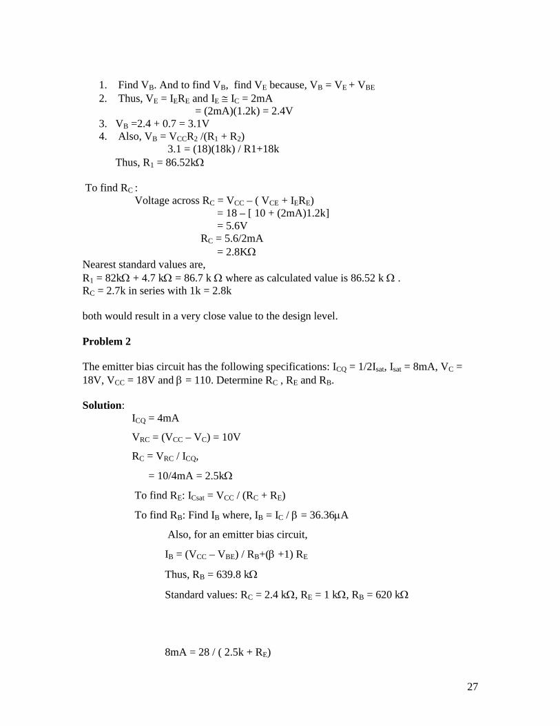
27
1. Find VB. And to find VB, find VE because, VB = VE + VBE
2. Thus, VE = IERE and IE IC = 2mA= (2mA)(1.2k) = 2.4V
3. VB =2.4 + 0.7 = 3.1V4. Also, VB = VCCR2 /(R1 + R2)
3.1 = (18)(18k) / R1+18kThus, R1 = 86.52k
To find RC :Voltage across RC = VCC – ( VCE + IERE)
= 18 – [ 10 + (2mA)1.2k]= 5.6V
RC = 5.6/2mA= 2.8K
Nearest standard values are,R1 = 82k + 4.7 k = 86.7 k where as calculated value is 86.52 k .RC = 2.7k in series with 1k = 2.8k
both would result in a very close value to the design level.
Problem 2
The emitter bias circuit has the following specifications: ICQ = 1/2Isat, Isat = 8mA, VC =18V, VCC = 18V and = 110. Determine RC , RE and RB.
Solution:ICQ = 4mA
VRC = (VCC – VC) = 10V
RC = VRC / ICQ,
= 10/4mA = 2.5k
To find RE: ICsat = VCC / (RC + RE)
To find RB: Find IB where, IB = IC / = 36.36A
Also, for an emitter bias circuit,
IB = (VCC – VBE) / RB+( +1) RE
Thus, RB = 639.8 k
Standard values: RC = 2.4 k, RE = 1 k, RB = 620 k
8mA = 28 / ( 2.5k + RE)

28
Thus, RE = 1k
Transistor switching networks:
Through proper design transistors can be used as switches for computer and controlapplications.When the input voltage VB is high ( logic 1), the transistor is in saturation ( ON). Andthe output at its collector = VCE is almost 0V( Logic 0)
Transistor as a switch
When the base voltage VB is low( logic 0), i.e, 0V, the transistor is cutoff( Off) and IC
is 0, drop across RC is 0 and therefore voltage at the collector is VCC.( logic 1)Thus transistor switch operates as an inverter.This circuit does not require any DC bias at the base of the transistor.
Design
When Vi ( VB) is 5V, transistor is in saturation and ICsat
Just before saturation, IB,max = IC,sat / DC
Thus the base current must be greater than IB,max to make the transistor to work insaturation.
Analysis
When Vi = 5V, the resulting level of IB is
IB = (Vi – 0.7) / RB
29
= ( 5 – 0.7) / 68k
= 63A
ICsat = VCC / RC = 5/0.82k
= 6.1mA
Verification
( IC,sat / ) = 48.8A
Thus IB > ( IC,sat / ) which is required for a transistor to be in saturation.
A transistor can be replaced by a low resistance Rsat when in saturation ( switch on)Rsat = VCE sat/ ICsat (VCE sat is very small and ICsat is IC,max is maximum current)A transistor can be replaced by a high resistance Rcutoff when in cutoff ( switch on)
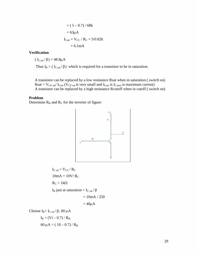
ProblemDetermine RB and RC for the inverter of figure:
IC sat = VCC / RC
10mA = 10V/ RC
RC = 1k
IB just at saturation = IC sat /
= 10mA / 250
= 40A
Choose IB> IC sat / , 60 A
IB = (Vi – 0.7) / RB
60 A = ( 10 – 0.7) / RB

30
RB = 155k
Choose RB = 150k, standard value,
re calculate IB, we get IB = 62 A which is also > IC sat /
Thus, RC = 1k and RB = 155k
Switching Transistors
Transistor ‘ON’ time = delay time + Rise timeDelay time is the time between the changing state of the input and the beginning of aresponse at the output.Rise time is the time from 10% to 90% of the final value.Transistor ‘OFF’ time = Storage time + Fall timeFor an ‘ON’ transistor, VBE should be around 0.7VFor the transistor to be in active region, VCE is usually about 25% to 75% of VCC.If VCE = almost VCC, probable faults:
– the device is damaged– connection in the collector – emitter or base – emitter circuit loop is open.
One of the most common mistake in the lab is usage of wrong resistor value.Check various voltages with respect to ground.Calculate the current values using voltage readings rather than measuring current bybreaking the circuit.
Problem – 1
Check the fault in the circuit given.
Problem - 2
31
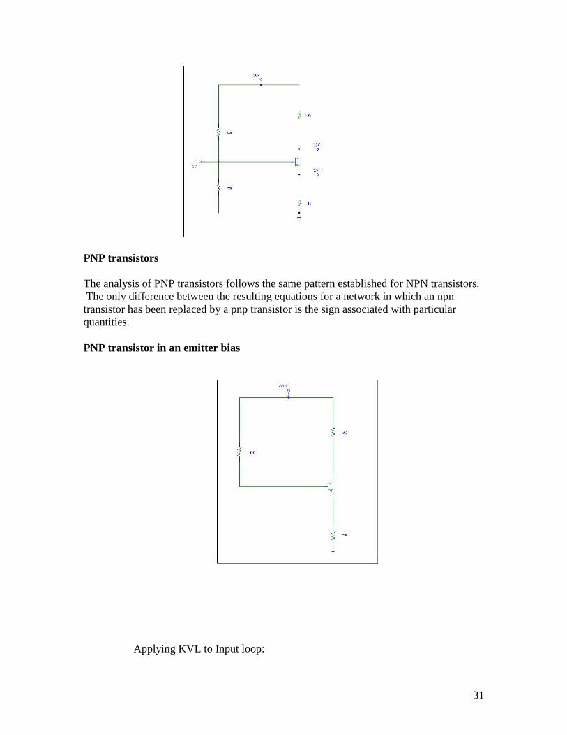
PNP transistors
The analysis of PNP transistors follows the same pattern established for NPN transistors.The only difference between the resulting equations for a network in which an npn
transistor has been replaced by a pnp transistor is the sign associated with particularquantities.
PNP transistor in an emitter bias
Applying KVL to Input loop:

32
VCC = IBRB +VBE+IERE
Thus, IB = (VCC – VBE) / [RB + (+1) RE]
Applying KVL Output loop:
VCE = - ( VCC – ICRC)
Bias stabilization
The stability of a system is a measure of the sensitivity of a network to variations inits parameters.In any amplifier employing a transistor the collector current IC is sensitive to each ofthe following parameters. increases with increase in temperature.Magnitude of VBE decreases about 2.5mV per degree Celsius increase in temperature.ICO doubles in value for every 10 degree Celsius increase in temperature.
T (degreeCelsius)
Ico (nA) VBE (V)
- 65 0.2 x 10⁻³ 20 0.85
25 0.1 50 0.65
100 20 80 0.48
175 3.3 x 10³ 120 0.3
Stability factors
S (ICO) = IC / IC0
S (VBE) = IC / VBE
S () = IC / Networks that are quite stable and relatively insensitive to temperature variationshave low stability factors.
The higher the stability factor, the more sensitive is the network to variations in thatparameter.

33
S( ICO)
• Analyze S( ICO) for– emitter bias configuration– fixed bias configuration– Voltage divider configuration
For the emitter bias configuration,
S( ICO) = ( + 1) [ 1 + RB / RE] / [( + 1) + RB / RE]
If RB / RE >> ( + 1) , then
S( ICO) = ( + 1)
For RB / RE <<1, S( ICO) 1
Thus, emitter bias configuration is quite stable when the ratio RB / RE is as small aspossible.Emitter bias configuration is least stable when RB / RE approaches ( + 1) .
Fixed bias configuration
S( ICO) = ( + 1) [ 1 + RB / RE] / [( + 1) + RB / RE]
= ( + 1) [RE + RB] / [( + 1) RE + RB]
By plugging RE = 0, we get
S( ICO) = + 1
This indicates poor stability.
Voltage divider configuration
S( ICO) = ( + 1) [ 1 + RB / RE] / [( + 1) + RB / RE]
Here, replace RB with Rth
S( ICO) = ( + 1) [ 1 + Rth / RE] / [( + 1) + Rth / RE]
Thus, voltage divider bias configuration is quite stable when the ratio Rth / RE is as small
as possible.

34
Physical impact
In a fixed bias circuit, IC increases due to increase in IC0. [IC = IB + (+1) IC0]IB is fixed by VCC and RB. Thus level of IC would continue to rise with temperature –a very unstable situation.
In emitter bias circuit, as IC increases, IE increases, VE increases. Increase in VE
reduces IB. IB = [VCC – VBE – VE] / RB. A drop in IB reduces IC.Thus, thisconfiguration is such that there is a reaction to an increase in IC that will tend tooppose the change in bias conditions.
In the DC bias with voltage feedback, as IC increases, voltage across RC increases,thus reducing IB and causing IC to reduce.
The most stable configuration is the voltage – divider network. If the condition RE
>>10R2, the voltage VB will remain fairly constant for changing levels of IC. VBE =VB – VE, as IC increases, VE increases, since VB is constant, VBE drops making IB tofall, which will try to offset the increases level of IC.
S(VBE)
S(VBE) = IC / VBE
For an emitter bias circuit, S(VBE) = - / [ RB + ( + 1)RE]
If RE =0 in the above equation, we get S(VBE) for a fixed bias circuit as,S(VBE) = - / RB.
For an emitter bias,
S(VBE) = - / [ RB + ( + 1)RE] can be rewritten as,
S(VBE) = - (/RE )/ [RB/RE + ( + 1)]
If ( + 1)>> RB/RE, thenS(VBE) = - (/RE )/ ( + 1)
= - 1/ RE
The larger the RE, lower the S(VBE) and more stable is the system.
Total effect of all the three parameters on IC can be written as,
IC = S(ICO) ICO + S(VBE) VBE + S()General conclusion:
The ratio RB / RE or Rth / RE should be as small as possible considering all aspects ofdesign.

35

36