Embed Size (px)
Citation preview

Microcontrollers
C166 Family16-Bit Single-Chip Microcontroller
C161PI
Data Sheet 1999-07 Preliminary
C161PI
ww
w.in
fineo
n.co
m

Edition 1999-07Published by Infineon Technologies AG i. Gr.,St.-Martin-Strasse 53D-81541 München© Infineon Technologies AG 1999.All Rights Reserved.Attention please!The information herein is given to describe certain components and shall not be considered as warranted characteristics.Terms of delivery and rights to technical change reserved.We hereby disclaim any and all warranties, including but not limited to warranties of non-infringement, regarding circuits, descriptions and charts stated herein.Infineon Technologies is an approved CECC manufacturer.InformationFor further information on technology, delivery terms and conditions and prices please contact your nearest Infineon Technologies Office in Germany or our Infineon Technologies Representatives worldwide (see address list).WarningsDue to technical requirements components may contain dangerous substances. For information on the types in question please contact your nearest Infineon Technologies Office.Infineon Technologies Components may only be used in life-support devices or systems with the express written approval of Infineon Tech-nologies, if a failure of such components can reasonably be expected to cause the failure of that life-support device or system, or to affect the safety or effectiveness of that device or system. Life support devices or systems are intended to be implanted in the human body, or to support and/or maintain and sustain and/or protect human life. If they fail, it is reasonable to assume that the health of the user or other persons may be endangered.
The C161PI is the successor of the C161RI. Therefore this data sheet also replaces the C161RIdata sheet (see also revision history).
C161PIRevision History: 1999-07 Preliminary
Previous Versions: 1998-05 (C161RI / Preliminary)1998-01 (C161RI / Advance Information)1997-12 (C161RI / Advance Information)
Page Subjects
--- 3 V specification introduced
4, 5, 7 Signal FOUT added
14 XRAM description added
15 Unlatched CS description added
23 Block Diagram corrected
24 Description of divider chain improved
25, 51, 52 ADC description updated to 10-bit
36, 37 Revised description of Absolute Max. Ratings and Operating Conditions
39, 44 Power supply values improved
45 - 50 Revised description for clock generation including PLL
54 ff. Standard 25-MHz timing
We Listen to Your CommentsAny information within this document that you feel is wrong, unclear or missing at all?Your feedback will help us to continuously improve the quality of this document.Please send your proposal (including a reference to this document) to:[email protected]

• High Performance 16-bit CPU with 4-Stage Pipeline– 80 ns Instruction Cycle Time at 25 MHz CPU Clock– 400 ns Multiplication (16 × 16 bit), 800 ns Division (32 / 16 bit)– Enhanced Boolean Bit Manipulation Facilities– Additional Instructions to Support HLL and Operating Systems– Register-Based Design with Multiple Variable Register Banks– Single-Cycle Context Switching Support– 16 MBytes Total Linear Address Space for Code and Data– 1024 Bytes On-Chip Special Function Register Area
• 16-Priority-Level Interrupt System with 27 Sources, Sample-Rate down to 40 ns• 8-Channel Interrupt-Driven Single-Cycle Data Transfer Facilities via
Peripheral Event Controller (PEC)• Clk. Generation via on-chip PLL (1:1.5/2/2.5/3/4/5), via prescaler or via direct clk. inp.• On-Chip Memory Modules
– 1 KByte On-Chip Internal RAM (IRAM)– 2 KBytes On-Chip Extension RAM (XRAM)
• On-Chip Peripheral Modules– 4-Channel 10-bit A/D Converter with Programm. Conversion Time down to 7.8 µs– Two Multi-Functional General Purpose Timer Units with 5 Timers– Two Serial Channels (Synchronous/Asynchronous and High-Speed-Synchronous)– I2C Bus Interface (10-bit Addressing, 400 KHz) with 2 Channels (multiplexed)
• Up to 8 MBytes External Address Space for Code and Data– Programmable External Bus Characteristics for Different Address Ranges– Multiplexed or Demultiplexed External Address/Data Buses with 8-Bit or 16-Bit
Data Bus Width– Five Programmable Chip-Select Signals
• Idle and Power Down Modes with Flexible Power Management• Programmable Watchdog Timer and Oscillator Watchdog• On-Chip Real Time Clock• Up to 76 General Purpose I/O Lines,
partly with Selectable Input Thresholds and Hysteresis• Supported by a Large Range of Development Tools like C-Compilers,
Macro-Assembler Packages, Emulators, Evaluation Boards, HLL-Debuggers,Simulators, Logic Analyzer Disassemblers, Programming Boards
• On-Chip Bootstrap Loader• 100-Pin MQFP / TQFP Package
Data Sheet 1 1999-07
C166 Family of C161PIHigh-Performance CMOS 16-Bit Microcontrollers
PreliminaryC161PI 16-Bit Microcontroller

&3,
Data Sheet 2 1999-07
This document describes the SAB-C161PI-LM, the SAB-C161PI-LF, the SAF-C161PI-LM and the SAF-C161PI-LF.For simplicity all versions are referred to by the term C161PI throughout this document.
Ordering Information
The ordering code for Infineon microcontrollers provides an exact reference to therequired product. This ordering code identifies:
• the derivative itself, i.e. its function set• the specified temperature range• the package• the type of delivery.
For the available ordering codes for the C161PI please refer to the„Product Catalog Microcontrollers“, which summarizes all available microcontrollervariants.
Note: The ordering codes for Mask-ROM versions are defined for each product afterverification of the respective ROM code.

&3,
Data Sheet 3 1999-07
Introduction
The C161PI is a derivative of the Infineon C166 Family of 16-bit single-chip CMOSmicrocontrollers. It combines high CPU performance (up to 8 million instructions persecond) with high peripheral functionality and enhanced IO-capabilities. The C161PIderivative is especially suited for cost sensitive applications.
Figure 1 Logic Symbol
C161PI
XTAL2
XTAL1
RSTIN
NMI
EA
RSTOUT
ALERDWR/WRL
VDD VSS
PORT016 bit
PORT116 bit
Port 28 bit
Port 315 bit
Port 47 bit
Port 68 bit
Port 56 bit
VAREF VAGND

&3,
Data Sheet 4 1999-07
Pin Configuration MQFP Package(top view)
Figure 2
807978777675747372717069686766656463626160595857565554535251
100
99 98 97 96 95 94 93 92 91 90 89 88 87 86 85 84 83 82 81
C161PI
123456789101112131415161718192021222324252627282930
31 32 33 34 35 36 37 38 39 40 41 42 43 44 45 46 47 48 49 50
NMIRSTOUTRSTINVDD
VSS
P1H.7/A15P1H.6/A14P1H.5/A13P1H.4/A12P1H.3/A11P1H.2/A10P1H.1/A9P1H.0/A8VDD
VSS
P1L.7/A7P1L.6/A6P1L.5/A5P1L.4/A4P1L.3/A3P1L.2/A2P1L.1/A1P1L.0/A0P0H.7/AD15P0H.6/AD14P0H.5/AD13P0H.4/AD12P0H.3/AD11P0H.2/AD10P0H.1/AD9
P5.2/AN2P5.3/AN3
P5.14/T4EUDP5.15/T2EUD
VSS
XTAL1XTAL2
VDD
P3.0/SCL0P3.1/SDA0
P3.2/CAPINP3.3/T3OUTP3.4/T3EUD
P3.5/T4INP3.6/T3INP3.7/T2IN
P3.8/MRSTP3.9/MTSRP3.10/TxD0P3.11/RxD0
P3.12/BHE/WRHP3.13/SCLK
P3.15/CLKOUT/FOUT VSS
VDD
P4.0/A16P4.1/A17P4.2/A18P4.3/A19P4.4/A20
P5.
1/A
N1
P5.
0/A
N0
VA
GN
D
VA
RE
F
P2.
15/E
X7I
NP
2.14
/EX
6IN
P2.
13/E
X5I
NP
2.12
/EX
4IN
P2.
11/E
X3I
NP
2.10
/EX
2IN
P2.
9/E
X1I
NP
2.8/
EX
0IN
P6.
7/S
DA
2P
6.6/
SC
L1P
6.5/
SD
A1
P6.
4/C
S4
P6.
3/C
S3
P6.
2/C
S2
P6.
1/C
S1
P6.
0/C
S0
P4.
5/A
21P
4.6/
A22 RD
WR
/WR
LR
EA
DY
ALE E
AV
SS
VD
D
P0L
.0/A
D0
P0L
.1/A
D1
P0L
.2/A
D2
P0L
.3/A
D3
P0L
.4/A
D4
P0L
.5/A
D5
P0L
.6/A
D6
P0L
.7/A
D7
VS
S
VD
D
P0H
.0/A
D8

&3,
Data Sheet 5 1999-07
Pin Configuration TQFP Package(top view)
Figure 3
P5.
3/A
N3
P5.
2/A
N2
P5.
1/A
N1
P5.
0/A
N0
VA
GN
D
VA
RE
F
P2.
15/E
X7I
NP
2.14
/EX
6IN
P2.
13/E
X5I
NP
2.12
/EX
4IN
P2.
11/E
X3I
NP
2.10
/EX
2IN
P2.
9/E
X1I
NP
2.8/
EX
0IN
P6.
7/S
DA
2P
6.6/
SC
L1P
6.5/
SD
A1
P6.
4/C
S4
P6.
3/C
S3
P6.
2/C
S2
P6.
1/C
S1
P6.
0/C
S0
NM
IR
ST
OU
TR
ST
IN
75747372717069686766656463626160595857565554535251
100
99 98 97 96 95 94 93 92 91 90 89 88 87 86 85 84 83 82 81 80 79 78 77 76
C161PI
12345678910111213141516171819202122232425
26 27 28 29 30 31 32 33 34 35 36 37 38 39 40 41 42 43 44 45 46 47 48 49 50
VDD
VSS
P1H.7/A15P1H.6/A14P1H.5/A13P1H.4/A12P1H.3/A11P1H.2/A10P1H.1/A9P1H.0/A8VDD
VSS
P1L.7/A7P1L.6/A6P1L.5/A5P1L.4/A4P1L.3/A3P1L.2/A2P1L.1/A1P1L.0/A0P0H.7/AD15P0H.6/AD14P0H.5/AD13P0H.4/AD12P0H.3/AD11
P5.14/T4EUDP5.15/T2EUD
VSS
XTAL1XTAL2
VDD
P3.0/SCL0P3.1/SDA0
P3.2/CAPINP3.3/T3OUTP3.4/T3EUD
P3.5/T4INP3.6/T3INP3.7/T2IN
P3.8/MRSTP3.9/MTSRP3.10/TxD0P3.11/RxD0
P3.12/BHE/WRHP3.13/SCLK
P3.15/CLKOUT/FOUT VSS
VDD
P4.0/A16P4.1/A17
P4.
2/A
18P
4.3/
A19
P4.
4/A
20P
4.5/
A21
P4.
6/A
22 RD
WR
/WR
LR
EA
DY
ALE E
AV
SS
VD
D
P0L
.0/A
D0
P0L
.1/A
D1
P0L
.2/A
D2
P0L
.3/A
D3
P0L
.4/A
D4
P0L
.5/A
D5
P0L
.6/A
D6
P0L
.7/A
D7
VS
S
VD
D
P0H
.0/A
D8
P0H
.1/A
D9
P0H
.2/A
D10

&3,
Data Sheet 6 1999-07
Table 1 Pin Definitions and Functions
Symbol Pin Num.TQFP
Pin Num.MQFP
InputOutp.
Function
P5
P5.0P5.1P5.2P5.3P5.14P5.15
97989910012
991001234
I
IIIIII
Port 5 is a 6-bit input-only port with Schmitt-Trigger characteristics. The pins of Port 5 also serve as (up to 4) analog input channels for the A/D converter, or they serve as timer inputs:AN0AN1AN2AN3T4EUD GPT1 Timer T4 Ext. Up/Down Ctrl. InputT2EUD GPT1 Timer T5 Ext. Up/Down Ctrl. Input
XTAL1
XTAL2
4
5
6
7
I
O
XTAL1: Input to the oscillator amplifier and input tothe internal clock generator
XTAL2: Output of the oscillator amplifier circuit.To clock the device from an external source, drive XTAL1, while leaving XTAL2 unconnected. Minimum and maximum high/low and rise/fall times specified in the AC Characteristics must be observed.
&3,
Data Sheet 7 1999-07
P3
P3.0P3.1P3.2P3.3P3.4P3.5
P3.6P3.7
P3.8P3.9P3.10P3.11P3.12
P3.13P3.15
789101112
1314
1516171819
2021
91011121314
1516
1718192021
2223
IO
I/OI/OIOII
II
I/OI/OOI/OOOI/OOO
Port 3 is a 15-bit bidirectional I/O port. It is bit-wise programmable for input or output via direction bits. For a pin configured as input, the output driver is put into high-impedance state. Port 3 outputs can be configured as push/pull or open drain drivers. The input threshold of Port 3 is selectable (TTL or special). The following Port 3 pins also serve for alternate functions:SCL0 I2C Bus Clock Line 0SDA0 I2C Bus Data Line 0CAPIN GPT2 Register CAPREL Capture InputT3OUT GPT1 Timer T3 Toggle Latch OutputT3EUD GPT1 Timer T3 External Up/Down Ctrl.InpT4IN GPT1 Timer T4 Count/Gate/Reload/
Capture InputT3IN GPT1 Timer T3 Count/Gate InputT2IN GPT1 Timer T2 Count/Gate/Reload/
Capture InputMRST SSC Master-Rec. / Slave-Trans. Inp/Outp.MTSR SSC Master-Trans. / Slave-Rec. Outp/Inp.T×D0 ASC0 Clock/Data Output (Async./Sync.)R×D0 ASC0 Data Input (Async.) or I/O (Sync.)BHE External Memory High Byte Enable Signal,WRH External Memory High Byte Write StrobeSCLK SSC Master Clock Outp. / Slave Clock Inp.CLKOUT System Clock Output (=CPU Clock)FOUT Programmable Frequency Output
Note: Pins P3.0 and P3.1 are open drain outputs only.
Table 1 Pin Definitions and Functions (continued)
Symbol Pin Num.TQFP
Pin Num.MQFP
InputOutp.
Function

&3,
Data Sheet 8 1999-07
P4
P4.0P4.1P4.2P4.3P4.4P4.5P4.6
24252627282930
26272829303132
IO
OOOOOOO
Port 4 is a 7-bit bidirectional I/O port. It is bit-wise programmable for input or output via direction bits. For a pin configured as input, the output driver is put into high-impedance state. Port 4 outputs can be configured as push/pull or open drain drivers. The input threshold of Port 4 is selectable (TTL or special). Port 4 can be used to output the segment address lines:A16 Least Significant Segment Address LineA17 Segment Address LineA18 Segment Address LineA19 Segment Address LineA20 Segment Address LineA21 Segment Address LineA22 Most Significant Segment Address Line
RD 31 33 O External Memory Read Strobe. RD is activated for every external instruction or data read access.
WR/WRL
32 34 O External Memory Write Strobe. In WR-mode this pin is activated for every external data write access. In WRL-mode this pin is activated for low byte data write accesses on a 16-bit bus, and for every data write access on an 8-bit bus. See WRCFG in register SYSCON for mode selection.
READY 33 35 I Ready Input. When the Ready function is enabled, a high level at this pin during an external memory access will force the insertion of memory cycle time waitstates until the pin returns to a low level.An internal pullup device will hold this pin high when nothing is driving it.
ALE 34 36 O Address Latch Enable Output. Can be used for latching the address into external memory or an address latch in the multiplexed bus modes.
Table 1 Pin Definitions and Functions (continued)
Symbol Pin Num.TQFP
Pin Num.MQFP
InputOutp.
Function
&3,
Data Sheet 9 1999-07
EA 35 37 I External Access Enable pin. A low level at this pin during and after Reset forces the C161PI to begin instruction execution out of external memory. A high level forces execution out of the internal program memory."ROMless" versions must have this pin tied to ‘0’.
PORT0P0L.0-7
P0H.0-7
38-4548-55
40-4750-57
IO PORT0 consists of the two 8-bit bidirectional I/O ports P0L and P0H. It is bit-wise programmable for input or output via direction bits. For a pin configured as input, the output driver is put into high-impedance state.In case of external bus configurations, PORT0 serves as the address (A) and address/data (AD) bus in multiplexed bus modes and as the data (D) bus in demultiplexed bus modes.Demultiplexed bus modes:Data Path Width: 8-bit 16-bitP0L.0 – P0L.7: D0 – D7 D0 - D7P0H.0 – P0H.7: I/O D8 - D15Multiplexed bus modes:Data Path Width: 8-bit 16-bitP0L.0 – P0L.7: AD0 – AD7 AD0 - AD7P0H.0 – P0H.7: A8 - A15 AD8 - AD15
PORT1P1L.0-7
P1H.0-7
56-6366-73
58-6568-75
IO PORT1 consists of the two 8-bit bidirectional I/O ports P1L and P1H. It is bit-wise programmable for input or output via direction bits. For a pin configured as input, the output driver is put into high-impedance state. PORT1 is used as the 16-bit address bus (A) in demultiplexed bus modes and also after switching from a demultiplexed bus mode to a multiplexed bus mode.
Table 1 Pin Definitions and Functions (continued)
Symbol Pin Num.TQFP
Pin Num.MQFP
InputOutp.
Function

&3,
Data Sheet 10 1999-07
RSTIN 76 78 I/O Reset Input with Schmitt-Trigger characteristics. A low level at this pin while the oscillator is running resets the C161PI. An internal pullup resistor permits power-on reset using only a capacitor connected to 9SS.A spike filter suppresses input pulses <10 ns. Input pulses >100 ns safely pass the filter.The minimum duration for a safe recognition should be 100 ns + 2 CPU clock cycles.In bidirectional reset mode (enabled by setting bit BDRSTEN in register SYSCON) the RSTIN line is internally pulled low for the duration of the internal reset sequence upon any reset (HW, SW, WDT).See note below this table.
Note: To let the reset configuration of PORT0 settleand to let the PLL lock a reset duration of ca.1 ms is recommended.
RST OUT
77 79 O Internal Reset Indication Output. This pin is set to a low level when the part is executing either a hardware-, a software- or a watchdog timer reset. RSTOUT remains low until the EINIT (end of initialization) instruction is executed.
NMI 78 80 I Non-Maskable Interrupt Input. A high to low transition at this pin causes the CPU to vector to the NMI trap routine. When the PWRDN (power down) instruction is executed, the NMI pin must be low in order to force the C161PI to go into power down mode. If NMI is high, when PWRDN is executed, the part will continue to run in normal mode.If not used, pin NMI should be pulled high externally.
Table 1 Pin Definitions and Functions (continued)
Symbol Pin Num.TQFP
Pin Num.MQFP
InputOutp.
Function

&3,
Data Sheet 11 1999-07
P6
P6.0P6.1P6.2P6.3P6.4P6.5P6.6P6.7
7980818283848586
8182838485868788
IO
OOOOOI/OI/OI/O
Port 6 is an 8-bit bidirectional I/O port. It is bit-wise programmable for input or output via direction bits. For a pin configured as input, the output driver is put into high-impedance state. Port 6 outputs can be configured as push/pull or open drain drivers.The Port 6 pins also serve for alternate functions:CS0 Chip Select 0 OutputCS1 Chip Select 1 OutputCS2 Chip Select 2 OutputCS3 Chip Select 3 OutputCS4 Chip Select 4 OutputSDA1 I2C Bus Data Line 1SCL1 I2C Bus Clock Line 1SDA2 I2C Bus Data Line 2
Note: Pins P6.7-5 are open drain outputs only.
P2
P2.8P2.9P2.10P2.11P2.12P2.13P2.14P2.15
8788899091929394
8990919293949596
IO
IIIIIIII
Port 2 is an 8-bit bidirectional I/O port. It is bit-wise programmable for input or output via direction bits. For a pin configured as input, the output driver is put into high-impedance state. Port 2 outputs can be configured as push/pull or open drain drivers. The input threshold of Port 2 is selectable (TTL or special).The Port 2 pins also serve for alternate functions:EX0IN Fast External Interrupt 0 InputEX1IN Fast External Interrupt 1 InputEX2IN Fast External Interrupt 2 InputEX3IN Fast External Interrupt 3 InputEX4IN Fast External Interrupt 4 InputEX5IN Fast External Interrupt 5 InputEX6IN Fast External Interrupt 6 InputEX7IN Fast External Interrupt 7 Input
9AREF 95 97 - Reference voltage for the A/D converter.
9AGND 96 98 - Reference ground for the A/D converter.
Table 1 Pin Definitions and Functions (continued)
Symbol Pin Num.TQFP
Pin Num.MQFP
InputOutp.
Function

&3,
Data Sheet 12 1999-07
Note: The following behaviour differences must be observed when the bidirectional resetis active:
• Bit BDRSTEN in register SYSCON cannot be changed after EINIT and is clearedautomatically after a reset.
• The reset indication flags always indicate a long hardware reset.• The PORT0 configuration is treated like on a hardware reset. Especially the bootstrap
loader may be activated when P0L.4 is low.• Pin RSTIN may only be connected to external reset devices with an open drain output
driver.• A short hardware reset is extended to the duration of the internal reset sequence.
9DD 6, 23, 37, 47, 65, 75
8, 25, 39, 49, 67, 77
- Digital Supply Voltage:+ 5 V or + 3 V during normal operation and idle mode.≥ 2.5 V during power down mode
9SS 3, 22, 36, 46, 64, 74
5, 24, 38, 48, 66, 76
- Digital Ground.
Table 1 Pin Definitions and Functions (continued)
Symbol Pin Num.TQFP
Pin Num.MQFP
InputOutp.
Function

&3,
Data Sheet 13 1999-07
Functional Description
The architecture of the C161PI combines advantages of both RISC and CISCprocessors and of advanced peripheral subsystems in a very well-balanced way. Thefollowing block diagram gives an overview of the different on-chip components and of theadvanced, high bandwidth internal bus structure of the C161PI.
Note: All time specifications refer to a CPU clock of 25 MHz(see definition in the AC Characteristics section).
Figure 4 Block Diagram
(nointernalROM) Instr./Data
3(&
&38&RUH
Interrupt Bus
InternalRAM
.%\WHDua
l Por
t
Port 2Port 3Port 4 Port 1
8
16
16Data
Data
32
Watchdog
Port 5
6C161RI V0.1
&38
&&RUH
XB
US
(16
-bit
NO
N M
UX
Dat
a / A
ddre
sses
)
16
External Instr./Data
16
USART
ASC
Sync.Channel
(SPI)
SSC
XTAL
15
BRGBRG
16
Peripheral Data
GPT 1
T 3
T 4
T 2
XRAM2 KByte
GPT 2
T 6
T 5
I²C-BusInterface
16
Interrupt Controller 11 ext. IR
OSC(input: 16MHz;
prescaleror direct drive)
ExternalBus
(MUXonly) &XBUS
Control,CS Logic
(4 CS)
16
Por
t 0P
ort 6
8
7
4-Channel
8-bitADC
RTC
Oscillator(16MHz)
PLL
10-bit

&3,
Data Sheet 14 1999-07
Memory Organization
The memory space of the C161PI is configured in a Von Neumann architecture whichmeans that code memory, data memory, registers and I/O ports are organized within thesame linear address space which includes 16 MBytes. The entire memory space can beaccessed bytewise or wordwise. Particular portions of the on-chip memory haveadditionally been made directly bitaddressable.
1 KByte of on-chip Internal RAM (IRAM) is provided as a storage for user definedvariables, for the system stack, general purpose register banks and even for code. Aregister bank can consist of up to 16 wordwide (R0 to R15) and/or bytewide (RL0, RH0,…, RL7, RH7) so-called General Purpose Registers (GPRs).
1024 bytes (2 * 512 bytes) of the address space are reserved for the Special FunctionRegister areas (SFR space and ESFR space). SFRs are wordwide registers which areused for controlling and monitoring functions of the different on-chip units. Unused SFRaddresses are reserved for future members of the C166 Family.
2 KBytes of on-chip Extension RAM (XRAM) are provided to store user data, userstacks, or code. The XRAM is accessed like external memory and therefore cannot beused for the system stack or for register banks and is not bitaddressable. The XRAMpermits 16-bit accesses with maximum speed.
In order to meet the needs of designs where more memory is required than is providedon chip, up to 8 MBytes of external RAM and/or ROM can be connected to themicrocontroller.

&3,
Data Sheet 15 1999-07
External Bus Controller
All of the external memory accesses are performed by a particular on-chip External BusController (EBC). It can be programmed either to Single Chip Mode when no externalmemory is required, or to one of four different external memory access modes, which areas follows:
– 16-/18-/20-/23-bit Addresses, 16-bit Data, Demultiplexed– 16-/18-/20-/23-bit Addresses, 16-bit Data, Multiplexed– 16-/18-/20-/23-bit Addresses, 8-bit Data, Multiplexed– 16-/18-/20-/23-bit Addresses, 8-bit Data, Demultiplexed
In the demultiplexed bus modes, addresses are output on PORT1 and data is input/output on PORT0 or P0L, respectively. In the multiplexed bus modes both addressesand data use PORT0 for input/output.
Important timing characteristics of the external bus interface (Memory Cycle Time,Memory Tri-State Time, Length of ALE and Read Write Delay) have been madeprogrammable to allow the user the adaption of a wide range of different types ofmemories and external peripherals.In addition, up to 4 independent address windows may be defined (via register pairsADDRSELx / BUSCONx) which allow to access different resources with different buscharacteristics. These address windows are arranged hierarchically where BUSCON4overrides BUSCON3 and BUSCON2 overrides BUSCON1. All accesses to locations notcovered by these 4 address windows are controlled by BUSCON0.Up to 5 external CS signals (4 windows plus default) can be generated in order to saveexternal glue logic. The C161PI offers the possibility to switch the CS outputs to anunlatched mode. In this mode the internal filter logic is switched off and the CS signalsare directly generated from the address. The unlatched CS mode is enabled by settingCSCFG (SYSCON.6).
Access to very slow memories is supported via a particular ‘Ready’ function.
For applications which require less than 8 MBytes of external memory space, thisaddress space can be restricted to 1 MByte, 256 KByte or to 64 KByte. In this case Port 4outputs four, two or no address lines at all. It outputs all 7 address lines, if an addressspace of 8 MBytes is used.

&3,
Data Sheet 16 1999-07
Central Processing Unit (CPU)
The main core of the CPU consists of a 4-stage instruction pipeline, a 16-bit arithmeticand logic unit (ALU) and dedicated SFRs. Additional hardware has been spent for aseparate multiply and divide unit, a bit-mask generator and a barrel shifter.
Based on these hardware provisions, most of the C161PI’s instructions can be executedin just one machine cycle which requires 2 CPU clocks (4 TCL). For example, shift androtate instructions are always processed during one machine cycle independent of thenumber of bits to be shifted. All multiple-cycle instructions have been optimized so thatthey can be executed very fast as well: branches in 2 cycles, a 16 × 16 bit multiplicationin 5 cycles and a 32-/16 bit division in 10 cycles. Another pipeline optimization, the so-called ‘Jump Cache’, reduces the execution time of repeatedly performed jumps in a loopfrom 2 cycles to 1 cycle.
Figure 5 CPU Block Diagram

&3,
Data Sheet 17 1999-07
The CPU has a register context consisting of up to 16 wordwide GPRs at its disposal.These 16 GPRs are physically allocated within the on-chip RAM area. A Context Pointer(CP) register determines the base address of the active register bank to be accessed bythe CPU at any time. The number of register banks is only restricted by the availableinternal RAM space. For easy parameter passing, a register bank may overlap others.
A system stack of up to 1024 bytes is provided as a storage for temporary data. Thesystem stack is allocated in the on-chip RAM area, and it is accessed by the CPU via thestack pointer (SP) register. Two separate SFRs, STKOV and STKUN, are implicitlycompared against the stack pointer value upon each stack access for the detection of astack overflow or underflow.
The high performance offered by the hardware implementation of the CPU can efficientlybe utilized by a programmer via the highly efficient C161PI instruction set which includesthe following instruction classes:
– Arithmetic Instructions– Logical Instructions– Boolean Bit Manipulation Instructions– Compare and Loop Control Instructions– Shift and Rotate Instructions– Prioritize Instruction– Data Movement Instructions– System Stack Instructions– Jump and Call Instructions– Return Instructions– System Control Instructions– Miscellaneous Instructions
The basic instruction length is either 2 or 4 bytes. Possible operand types are bits, bytesand words. A variety of direct, indirect or immediate addressing modes are provided tospecify the required operands.

&3,
Data Sheet 18 1999-07
Interrupt System
With an interrupt response time within a range from just 5 to 12 CPU clocks (in case ofinternal program execution), the C161PI is capable of reacting very fast to theoccurrence of non-deterministic events.
The architecture of the C161PI supports several mechanisms for fast and flexibleresponse to service requests that can be generated from various sources internal orexternal to the microcontroller. Any of these interrupt requests can be programmed tobeing serviced by the Interrupt Controller or by the Peripheral Event Controller (PEC).
In contrast to a standard interrupt service where the current program execution issuspended and a branch to the interrupt vector table is performed, just one cycle is‘stolen’ from the current CPU activity to perform a PEC service. A PEC service implies asingle byte or word data transfer between any two memory locations with an additionalincrement of either the PEC source or the destination pointer. An individual PEC transfercounter is implicity decremented for each PEC service except when performing in thecontinuous transfer mode. When this counter reaches zero, a standard interrupt isperformed to the corresponding source related vector location. PEC services are verywell suited, for example, for supporting the transmission or reception of blocks of data.The C161PI has 8 PEC channels each of which offers such fast interrupt-driven datatransfer capabilities.
A separate control register which contains an interrupt request flag, an interrupt enableflag and an interrupt priority bitfield exists for each of the possible interrupt sources. Viaits related register, each source can be programmed to one of sixteen interrupt prioritylevels. Once having been accepted by the CPU, an interrupt service can only beinterrupted by a higher prioritized service request. For the standard interrupt processing,each of the possible interrupt sources has a dedicated vector location.
Fast external interrupt inputs are provided to service external interrupts with highprecision requirements. These fast interrupt inputs feature programmable edgedetection (rising edge, falling edge or both edges).
Software interrupts are supported by means of the ‘TRAP’ instruction in combination withan individual trap (interrupt) number.
The following table shows all of the possible C161PI interrupt sources and thecorresponding hardware-related interrupt flags, vectors, vector locations and trap(interrupt) numbers.
Note: Interrupt nodes which are not used by associated peripherals, may be used togenerate software controlled interrupt requests by setting the respective interruptrequest bit (xIR).

&3,
Data Sheet 19 1999-07
Table 2 C161PI Interrupt Nodes
Source of Interrupt or PEC Service Request
RequestFlag
EnableFlag
InterruptVector
VectorLocation
TrapNumber
External Interrupt 0 CC8IR CC8IE CC8INT 00’0060H 18H
External Interrupt 1 CC9IR CC9IE CC9INT 00’0064H 19H
External Interrupt 2 CC10IR CC10IE CC10INT 00’0068H 1AH
External Interrupt 3 CC11IR CC11IE CC11INT 00’006CH 1BH
External Interrupt 4 CC12IR CC12IE CC12INT 00’0070H 1CH
External Interrupt 5 CC13IR CC13IE CC13INT 00’0074H 1DH
External Interrupt 6 CC14IR CC14IE CC14INT 00’0078H 1EH
External Interrupt 7 CC15IR CC15IE CC15INT 00’007CH 1FH
GPT1 Timer 2 T2IR T2IE T2INT 00’0088H 22H
GPT1 Timer 3 T3IR T3IE T3INT 00’008CH 23H
GPT1 Timer 4 T4IR T4IE T4INT 00’0090H 24H
GPT2 Timer 5 T5IR T5IE T5INT 00’0094H 25H
GPT2 Timer 6 T6IR T6IE T6INT 00’0098H 26H
GPT2 CAPREL Register
CRIR CRIE CRINT 00’009CH 27H
A/D Conversion Complete
ADCIR ADCIE ADCINT 00’00A0H 28H
A/D Overrun Error ADEIR ADEIE ADEINT 00’00A4H 29H
ASC0 Transmit S0TIR S0TIE S0TINT 00’00A8H 2AH
ASC0 Transmit Buffer S0TBIR S0TBIE S0TBINT 00’011CH 47H
ASC0 Receive S0RIR S0RIE S0RINT 00’00ACH 2BH
ASC0 Error S0EIR S0EIE S0EINT 00’00B0H 2CH
SSC Transmit SCTIR SCTIE SCTINT 00’00B4H 2DH
SSC Receive SCRIR SCRIE SCRINT 00’00B8H 2EH
SSC Error SCEIR SCEIE SCEINT 00’00BCH 2FH
I2C Data Transfer Event
XP0IR XP0IE XP0INT 00’0100H 40H
I2C Protocol Event XP1IR XP1IE XP1INT 00’0104H 41H
X-Peripheral Node 2 XP2IR XP2IE XP2INT 00’0108H 42H
PLL Unlock / RTC XP3IR XP3IE XP3INT 00’010CH 43H

&3,
Data Sheet 20 1999-07
The C161PI also provides an excellent mechanism to identify and to process exceptionsor error conditions that arise during run-time, so-called ‘Hardware Traps’. Hardwaretraps cause immediate non-maskable system reaction which is similar to a standardinterrupt service (branching to a dedicated vector table location). The occurence of ahardware trap is additionally signified by an individual bit in the trap flag register (TFR).Except when another higher prioritized trap service is in progress, a hardware trap willinterrupt any actual program execution. In turn, hardware trap services can normally notbe interrupted by standard or PEC interrupts.
The following table shows all of the possible exceptions or error conditions that can ariseduring run-time:
Table 3 Hardware Trap Summary
Exception Condition TrapFlag
TrapVector
VectorLocation
TrapNumber
TrapPrio
Reset Functions:Hardware ResetSoftware ResetWatchdog Timer Overflow
RESETRESETRESET
00’0000H
00’0000H
00’0000H
00H
00H
00H
IIIIIIIII
Class A Hardware Traps:Non-Maskable InterruptStack OverflowStack Underflow
NMISTKOFSTKUF
NMITRAPSTOTRAPSTUTRAP
00’0008H
00’0010H
00’0018H
02H
04H
06H
IIIIII
Class B Hardware Traps:Undefined OpcodeProtected Instruction FaultIllegal Word Operand AccessIllegal Instruction AccessIllegal External Bus Access
UNDOPCPRTFLTILLOPAILLINAILLBUS
BTRAPBTRAPBTRAPBTRAPBTRAP
00’0028H
00’0028H
00’0028H
00’0028H
00’0028H
0AH
0AH
0AH
0AH
0AH
IIIII
Reserved [2CH – 3CH] [0BH – 0FH]
Software Traps:TRAP Instruction
Any[00’0000H – 00’01FCH]in stepsof 4H
Any[00H – 7FH]
CurrentCPU Priority

&3,
Data Sheet 21 1999-07
General Purpose Timer (GPT) Unit
The GPT unit represents a very flexible multifunctional timer/counter structure whichmay be used for many different time related tasks such as event timing and counting,pulse width and duty cycle measurements, pulse generation, or pulse multiplication.
The GPT unit incorporates five 16-bit timers which are organized in two separatemodules, GPT1 and GPT2. Each timer in each module may operate independently in anumber of different modes, or may be concatenated with another timer of the samemodule.
Each of the three timers T2, T3, T4 of module GPT1 can be configured individually forone of four basic modes of operation, which are Timer, Gated Timer, Counter, andIncremental Interface Mode. In Timer Mode, the input clock for a timer is derived fromthe CPU clock, divided by a programmable prescaler, while Counter Mode allows a timerto be clocked in reference to external events.Pulse width or duty cycle measurement is supported in Gated Timer Mode, where theoperation of a timer is controlled by the ‘gate’ level on an external input pin. For thesepurposes, each timer has one associated port pin (TxIN) which serves as gate or clockinput. The maximum resolution of the timers in module GPT1 is 16 TCL.
The count direction (up/down) for each timer is programmable by software or mayadditionally be altered dynamically by an external signal on a port pin (TxEUD) tofacilitate eg. position tracking.
In Incremental Interface Mode the GPT1 timers (T2, T3, T4) can be directly connectedto the incremental position sensor signals A and B via their respective inputs TxIN andTxEUD. Direction and count signals are internally derived from these two input signals,so the contents of the respective timer Tx corresponds to the sensor position. The thirdposition sensor signal TOP0 can be connected to an interrupt input.
Timer T3 has an output toggle latch (T3OTL) which changes its state on each timer over-flow/underflow. The state of this latch may be output on a port pin (T3OUT) eg. for timeout monitoring of external hardware components, or may be used internally to clocktimers T2 and T4 for measuring long time periods with high resolution.
In addition to their basic operating modes, timers T2 and T4 may be configured as reloador capture registers for timer T3. When used as capture or reload registers, timers T2and T4 are stopped. The contents of timer T3 are captured into T2 or T4 in response toa signal at their associated input pins (TxIN). Timer T3 is reloaded with the contents ofT2 or T4 triggered either by an external signal or by a selectable state transition of itstoggle latch T3OTL. When both T2 and T4 are configured to alternately reload T3 onopposite state transitions of T3OTL with the low and high times of a PWM signal, thissignal can be constantly generated without software intervention.

&3,
Data Sheet 22 1999-07
Figure 6 Block Diagram of GPT1
With its maximum resolution of 8 TCL, the GPT2 module provides precise event controland time measurement. It includes two timers (T5, T6) and a capture/reload register(CAPREL). Both timers can be clocked with an input clock which is derived from the CPUclock via a programmable prescaler. The count direction (up/down) for each timer isprogrammable by software. Concatenation of the timers is supported via the outputtoggle latch (T6OTL) of timer T6, which changes its state on each timer overflow/underflow.
T3Mode
Control
2n : 1fCPU
2n : 1fCPU T2Mode
Control
GPT1 Timer T2
Reload
Capture
2n : 1fCPU
T4Mode
Control GPT1 Timer T4
Reload
Capture
GPT1 Timer T3 T3OTL
U/D
T2EUD
T2IN
T3IN
T3EUD
T4IN
T4EUD
T3OUT
Toggle FF
U/D
U/D
InterruptRequest
InterruptRequest
InterruptRequest
OtherTimers
MCT02141

&3,
Data Sheet 23 1999-07
The state of this latch may be used to clock timer T5. The overflows/underflows of timerT6 can additionally be used to cause a reload from the CAPREL register. The CAPRELregister may capture the contents of timer T5 based on an external signal transition onthe corresponding port pin (CAPIN), and timer T5 may optionally be cleared after thecapture procedure. This allows absolute time differences to be measured or pulsemultiplication to be performed without software overhead.
The capture trigger (timer T5 to CAPREL) may also be generated upon transitions ofGPT1 timer T3’s inputs T3IN and/or T3EUD. This is especially advantageous when T3operates in Incremental Interface Mode.
Figure 7 Block Diagram of GPT2
MUX
2n : 1fCPUT5
ModeControl
GPT2 Timer T5
2n : 1fCPU
T6Mode
Control
GPT2 Timer T6
GPT2 CAPREL
T6OTL
T3
CAPIN
T6OUT
U/D
U/D
InterruptRequest
InterruptRequest
InterruptRequest
OtherTimers
Clear
Capture
CT3
Mcb03999C.vsd

&3,
Data Sheet 24 1999-07
Real Time Clock
The Real Time Clock (RTC) module of the C161PI consists of a chain of 3 divider blocks,a fixed 8:1 divider, the reloadable 16-bit timer T14, and the 32-bit RTC timer (accessiblevia registers RTCH and RTCL). The RTC module is directly clocked with the on-chiposcillator frequency divided by 32 via a separate clock driver (IRTC = IOSC / 32) and istherefore independent from the selected clock generation mode of the C161PI. All timerscount up.
The RTC module can be used for different purposes:
• System clock to determine the current time and date• Cyclic time based interrupt• 48-bit timer for long term measurements
Figure 8 RTC Block Diagram
Note: The registers associated with the RTC are not effected by a reset in order tomaintain the correct system time even when intermediate resets are executed.
RTCLRTCL
T14
T14REL
8:1fRTC
Reload
InterruptRequest

&3,
Data Sheet 25 1999-07
A/D Converter
For analog signal measurement, a 10-bit A/D converter with 4 multiplexed input channelsand a sample and hold circuit has been integrated on-chip. It uses the method ofsuccessive approximation. The sample time (for loading the capacitors) and theconversion time is programmable and can so be adjusted to the external circuitry.
Overrun error detection/protection is provided for the conversion result register(ADDAT): either an interrupt request will be generated when the result of a previousconversion has not been read from the result register at the time the next conversion iscomplete, or the next conversion is suspended in such a case until the previous resulthas been read.
For applications which require less than 4 analog input channels, the remaining channelinputs can be used as digital input port pins.
The A/D converter of the C161PI supports four different conversion modes. In thestandard Single Channel conversion mode, the analog level on a specified channel issampled once and converted to a digital result. In the Single Channel Continuous mode,the analog level on a specified channel is repeatedly sampled and converted withoutsoftware intervention. In the Auto Scan mode, the analog levels on a prespecifiednumber of channels are sequentially sampled and converted. In the Auto ScanContinuous mode, the number of prespecified channels is repeatedly sampled andconverted. In addition, the conversion of a specific channel can be inserted (injected) intoa running sequence without disturbing this sequence. This is called Channel InjectionMode.
The Peripheral Event Controller (PEC) may be used to automatically store theconversion results into a table in memory for later evaluation, without requiring theoverhead of entering and exiting interrupt routines for each data transfer.
After each reset and also during normal operation the ADC automatically performscalibration cycles. This automatic self-calibration constantly adjusts the converter tochanging operating conditions (e.g. temperature) and compensates process variations.
These calibration cycles are part of the conversion cycle, so they do not affect the normaloperation of the A/D converter.
In order to decouple analog inputs from digital noise and to avoid input trigger noisethose pins used for analog input can be disconnected from the digital IO or input stagesunder software control. This can be selected for each pin separately via registersP5DIDIS (Port 5 Digital Input Disable).

&3,
Data Sheet 26 1999-07
Serial Channels
Serial communication with other microcontrollers, processors, terminals or externalperipheral components is provided by two serial interfaces with different functionality, anAsynchronous/Synchronous Serial Channel (ASC0) and a High-Speed SynchronousSerial Channel (SSC).
The ASC0 is upward compatible with the serial ports of the Infineon 8-bit microcontrollerfamilies and supports full-duplex asynchronous communication at up to 780 KBaud andhalf-duplex synchronous communication at up to 3.1 MBaud @ 25 MHz CPU clock.A dedicated baud rate generator allows to set up all standard baud rates withoutoscillator tuning. For transmission, reception and error handling 4 separate interruptvectors are provided. In asynchronous mode, 8- or 9-bit data frames are transmitted orreceived, preceded by a start bit and terminated by one or two stop bits. Formultiprocessor communication, a mechanism to distinguish address from data bytes hasbeen included (8-bit data plus wake up bit mode).In synchronous mode, the ASC0 transmits or receives bytes (8 bits) synchronously to ashift clock which is generated by the ASC0. The ASC0 always shifts the LSB first. A loopback option is available for testing purposes.A number of optional hardware error detection capabilities has been included to increasethe reliability of data transfers. A parity bit can automatically be generated ontransmission or be checked on reception. Framing error detection allows to recognizedata frames with missing stop bits. An overrun error will be generated, if the lastcharacter received has not been read out of the receive buffer register at the time thereception of a new character is complete.
The SSC supports full-duplex synchronous communication at up to 6.25 Mbaud @25 MHz CPU clock. It may be configured so it interfaces with serially linked peripheralcomponents. A dedicated baud rate generator allows to set up all standard baud rateswithout oscillator tuning. For transmission, reception and error handling 3 separateinterrupt vectors are provided.The SSC transmits or receives characters of 2...16 bits length synchronously to a shiftclock which can be generated by the SSC (master mode) or by an external master (slavemode). The SSC can start shifting with the LSB or with the MSB and allows the selectionof shifting and latching clock edges as well as the clock polarity.A number of optional hardware error detection capabilities has been included to increasethe reliability of data transfers. Transmit and receive error supervise the correct handlingof the data buffer. Phase and baudrate error detect incorrect serial data.

&3,
Data Sheet 27 1999-07
I2C Module
The integrated I2C Bus Module handles the transmission and reception of frames overthe two-line I2C bus in accordance with the I2C Bus specification. The on-chip I2C Modulecan receive and transmit data using 7-bit or 10-bit addressing and it can operate in slavemode, in master mode or in multi-master mode.
Several physical interfaces (port pins) can be established under software control. Datacan be transferred at speeds up to 400 Kbit/sec.
Two interrupt nodes dedicated to the I2C module allow efficient interrupt service and alsosupport operation via PEC transfers.
Note: The port pins associated with the I2C interfaces feature open drain drivers only, asrequired by the I2C specification.
Watchdog Timer
The Watchdog Timer represents one of the fail-safe mechanisms which have beenimplemented to prevent the controller from malfunctioning for longer periods of time.
The Watchdog Timer is always enabled after a reset of the chip, and can only bedisabled in the time interval until the EINIT (end of initialization) instruction has beenexecuted. Thus, the chip’s start-up procedure is always monitored. The software has tobe designed to service the Watchdog Timer before it overflows. If, due to hardware orsoftware related failures, the software fails to do so, the Watchdog Timer overflows andgenerates an internal hardware reset and pulls the RSTOUT pin low in order to allowexternal hardware components to be reset.
The Watchdog Timer is a 16-bit timer, clocked with the system clock divided either by 2or by 128. The high byte of the Watchdog Timer register can be set to a prespecifiedreload value (stored in WDTREL) in order to allow further variation of the monitored timeinterval. Each time it is serviced by the application software, the high byte of theWatchdog Timer is reloaded. Thus, time intervals between 20 µs and 336 ms can bemonitored (@ 25 MHz).The default Watchdog Timer interval after reset is 5.24 ms (@ 25 MHz).

&3,
Data Sheet 28 1999-07
Parallel Ports
The C161PI provides up to 76 IO lines which are organized into six input/output portsand one input port. All port lines are bit-addressable, and all input/output lines areindividually (bit-wise) programmable as inputs or outputs via direction registers. The I/Oports are true bidirectional ports which are switched to high impedance state whenconfigured as inputs. The output drivers of three IO ports can be configured (pin by pin)for push/pull operation or open-drain operation via control registers. The other IO portsoperate in push/pull mode, except for the I²C interface pins which are open drain pinsonly. During the internal reset, all port pins are configured as inputs.
All port lines have programmable alternate input or output functions associated withthem. All port lines that are not used for these alternate functions may be used as generalpurpose IO lines.
PORT0 and PORT1 may be used as address and data lines when accessing externalmemory, while Port 4 outputs the additional segment address bits A22/19/17...A16 insystems where segmentation is enabled to access more than 64 KBytes of memory.
Port 3 includes alternate functions of timers, serial interfaces, the optional bus controlsignal BHE and the system clock output CLKOUT (or the programmable frequencyoutput FOUT).Port 5 is used for the analog input channels to the A/D converter or timer control signals.
Port 6 provides the optional chip select signals and interface lines for the I²C module.
The edge characteristics (transition time) of the C161PI’s port drivers can be selectedvia the Port Driver Control Register (PDCR).

&3,
Data Sheet 29 1999-07
Instruction Set Summary
The table below lists the instructions of the C161PI in a condensed way.The various addressing modes that can be used with a specific instruction, the operationof the instructions, parameters for conditional execution of instructions, and the opcodesfor each instruction can be found in the “C166 Family Instruction Set Manual” .
This document also provides a detailled description of each instruction.
Table 4 Instruction Set Summary
Mnemonic Description BytesADD(B) Add word (byte) operands 2 / 4
ADDC(B) Add word (byte) operands with Carry 2 / 4
SUB(B) Subtract word (byte) operands 2 / 4
SUBC(B) Subtract word (byte) operands with Carry 2 / 4
MUL(U) (Un)Signed multiply direct GPR by direct GPR (16-16-bit) 2
DIV(U) (Un)Signed divide register MDL by direct GPR (16-/16-bit) 2
DIVL(U) (Un)Signed long divide reg. MD by direct GPR (32-/16-bit) 2
CPL(B) Complement direct word (byte) GPR 2
NEG(B) Negate direct word (byte) GPR 2
AND(B) Bitwise AND, (word/byte operands) 2 / 4
OR(B) Bitwise OR, (word/byte operands) 2 / 4
XOR(B) Bitwise XOR, (word/byte operands) 2 / 4
BCLR Clear direct bit 2
BSET Set direct bit 2
BMOV(N) Move (negated) direct bit to direct bit 4
BAND, BOR, BXOR
AND/OR/XOR direct bit with direct bit 4
BCMP Compare direct bit to direct bit 4
BFLDH/L Bitwise modify masked high/low byte of bit-addressable direct word memory with immediate data
4
CMP(B) Compare word (byte) operands 2 / 4
CMPD1/2 Compare word data to GPR and decrement GPR by 1/2 2 / 4
CMPI1/2 Compare word data to GPR and increment GPR by 1/2 2 / 4
PRIOR Determine number of shift cycles to normalize directword GPR and store result in direct word GPR
2
SHL / SHR Shift left/right direct word GPR 2
ROL / ROR Rotate left/right direct word GPR 2
ASHR Arithmetic (sign bit) shift right direct word GPR 2

&3,
Data Sheet 30 1999-07
MOV(B) Move word (byte) data 2 / 4
MOVBS Move byte operand to word operand with sign extension 2 / 4
MOVBZ Move byte operand to word operand. with zero extension 2 / 4
JMPA, JMPI, JMPR
Jump absolute/indirect/relative if condition is met 4
JMPS Jump absolute to a code segment 4
J(N)B Jump relative if direct bit is (not) set 4
JBC Jump relative and clear bit if direct bit is set 4
JNBS Jump relative and set bit if direct bit is not set 4
CALLA, CALLI, CALLR
Call absolute/indirect/relative subroutine if condition is met 4
CALLS Call absolute subroutine in any code segment 4
PCALL Push direct word register onto system stack and callabsolute subroutine
4
TRAP Call interrupt service routine via immediate trap number 2
PUSH, POP Push/pop direct word register onto/from system stack 2
SCXT Push direct word register onto system stack und updateregister with word operand
4
RET Return from intra-segment subroutine 2
RETS Return from inter-segment subroutine 2
RETP Return from intra-segment subroutine and pop directword register from system stack
2
RETI Return from interrupt service subroutine 2
SRST Software Reset 4
IDLE Enter Idle Mode 4
PWRDN Enter Power Down Mode (supposes NMI-pin being low) 4
SRVWDT Service Watchdog Timer 4
DISWDT Disable Watchdog Timer 4
EINIT Signify End-of-Initialization on RSTOUT-pin 4
ATOMIC Begin ATOMIC sequence 2
EXTR Begin EXTended Register sequence 2
EXTP(R) Begin EXTended Page (and Register) sequence 2 / 4
EXTS(R) Begin EXTended Segment (and Register) sequence 2 / 4
NOP Null operation 2
Table 4 Instruction Set Summary (continued)
Mnemonic Description Bytes

&3,
Data Sheet 31 1999-07
Special Function Registers Overview
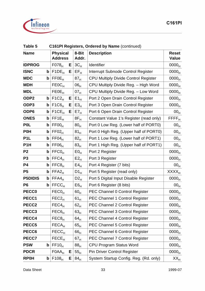
The following table lists all SFRs which are implemented in the C161PI in alphabeticalorder.Bit-addressable SFRs are marked with the letter “b” in column “Name”. SFRs within theExtended SFR-Space (ESFRs) are marked with the letter “E” in column “PhysicalAddress”. Registers within on-chip X-Peripherals (I²C) are marked with the letter “X” incolumn “Physical Address”.
An SFR can be specified via its individual mnemonic name. Depending on the selectedaddressing mode, an SFR can be accessed via its physical address (using the DataPage Pointers), or via its short 8-bit address (without using the Data Page Pointers).
Table 5 C161PI Registers, Ordered by Name
Name PhysicalAddress
8-BitAddr.
Description ResetValue
ADCIC b FF98H CCH A/D Converter End of Conversion Interrupt Control Register
0000H
ADCON b FFA0H D0H A/D Converter Control Register 0000H
ADDAT FEA0H 50H A/D Converter Result Register 0000H
ADDAT2 F0A0H E 50H A/D Converter 2 Result Register 0000H
ADDRSEL1 FE18H 0CH Address Select Register 1 0000H
ADDRSEL2 FE1AH 0DH Address Select Register 2 0000H
ADDRSEL3 FE1CH 0EH Address Select Register 3 0000H
ADDRSEL4 FE1EH 0FH Address Select Register 4 0000H
ADEIC b FF9AH CDH A/D Converter Overrun Error Interrupt Control Register
0000H
BUSCON0 b FF0CH 86H Bus Configuration Register 0 0000H
BUSCON1 b FF14H 8AH Bus Configuration Register 1 0000H
BUSCON2 b FF16H 8BH Bus Configuration Register 2 0000H
BUSCON3 b FF18H 8CH Bus Configuration Register 3 0000H
BUSCON4 b FF1AH 8DH Bus Configuration Register 4 0000H
CAPREL FE4AH 25H GPT2 Capture/Reload Register 0000H
CC8IC b FF88H C4H External Interrupt 0 Control Register 0000H
CC9IC b FF8AH C5H External Interrupt 1 Control Register 0000H
CC10IC b FF8CH C6H External Interrupt 2 Control Register 0000H
CC11IC b FF8EH C7H External Interrupt 3 Control Register 0000H

&3,
Data Sheet 32 1999-07
CC12IC b FF90H C8H External Interrupt 4 Control Register 0000H
CC13IC b FF92H C9H External Interrupt 5 Control Register 0000H
CC14IC b FF94H CAH External Interrupt 6 Control Register 0000H
CC15IC b FF96H CBH External Interrupt 7 Control Register 0000H
CP FE10H 08H CPU Context Pointer Register FC00H
CRIC b FF6AH B5H GPT2 CAPREL Interrupt Ctrl. Register 0000H
CSP FE08H 04H CPU Code Segment Pointer Register(8 bits, not directly writeable)
0000H
DP0L b F100H E 80H P0L Direction Control Register 00H
DP0H b F102H E 81H P0H Direction Control Register 00H
DP1L b F104H E 82H P1L Direction Control Register 00H
DP1H b F106H E 83H P1H Direction Control Register 00H
DP2 b FFC2H E1H Port 2 Direction Control Register 0000H
DP3 b FFC6H E3H Port 3 Direction Control Register 0000H
DP4 b FFCAH E5H Port 4 Direction Control Register 00H
DP6 b FFCEH E7H Port 6 Direction Control Register 00H
DPP0 FE00H 00H CPU Data Page Pointer 0 Register (10 bits)
0000H
DPP1 FE02H 01H CPU Data Page Pointer 1 Reg. (10 bits) 0001H
DPP2 FE04H 02H CPU Data Page Pointer 2 Reg. (10 bits) 0002H
DPP3 FE06H 03H CPU Data Page Pointer 3 Reg. (10 bits) 0003H
EXICON b F1C0H E E0H External Interrupt Control Register 0000H
ICADR ED06H X --- I²C Address Register 0XXXH
ICCFG ED00H X --- I²C Configuration Register XX00H
ICCON ED02H X --- I²C Control Register 0000H
ICRTB ED08H X --- I²C Receive/Transmit Buffer XXH
ICST ED04H X --- I²C Status Register 0000H
IDCHIP F07CH E 3EH Identifier 09XXH
IDMANUF F07EH E 3FH Identifier 1820H
IDMEM F07AH E 3DH Identifier 0000H
Table 5 C161PI Registers, Ordered by Name (continued)
Name PhysicalAddress
8-BitAddr.
Description ResetValue
&3,
Data Sheet 33 1999-07
IDPROG F078H E 3CH Identifier 0000H
ISNC b F1DEH E EFH Interrupt Subnode Control Register 0000H
MDC b FF0EH 87H CPU Multiply Divide Control Register 0000H
MDH FE0CH 06H CPU Multiply Divide Reg. – High Word 0000H
MDL FE0EH 07H CPU Multiply Divide Reg. – Low Word 0000H
ODP2 b F1C2H E E1H Port 2 Open Drain Control Register 0000H
ODP3 b F1C6H E E3H Port 3 Open Drain Control Register 0000H
ODP6 b F1CEH E E7H Port 6 Open Drain Control Register 00H
ONES b FF1EH 8FH Constant Value 1’s Register (read only) FFFFH
P0L b FF00H 80H Port 0 Low Reg. (Lower half of PORT0) 00H
P0H b FF02H 81H Port 0 High Reg. (Upper half of PORT0) 00H
P1L b FF04H 82H Port 1 Low Reg. (Lower half of PORT1) 00H
P1H b FF06H 83H Port 1 High Reg. (Upper half of PORT1) 00H
P2 b FFC0H E0H Port 2 Register 0000H
P3 b FFC4H E2H Port 3 Register 0000H
P4 b FFC8H E4H Port 4 Register (7 bits) 00H
P5 b FFA2H D1H Port 5 Register (read only) XXXXH
P5DIDIS b FFA4H D2H Port 5 Digital Input Disable Register 0000H
P6 b FFCCH E6H Port 6 Register (8 bits) 00H
PECC0 FEC0H 60H PEC Channel 0 Control Register 0000H
PECC1 FEC2H 61H PEC Channel 1 Control Register 0000H
PECC2 FEC4H 62H PEC Channel 2 Control Register 0000H
PECC3 FEC6H 63H PEC Channel 3 Control Register 0000H
PECC4 FEC8H 64H PEC Channel 4 Control Register 0000H
PECC5 FECAH 65H PEC Channel 5 Control Register 0000H
PECC6 FECCH 66H PEC Channel 6 Control Register 0000H
PECC7 FECEH 67H PEC Channel 7 Control Register 0000H
PSW b FF10H 88H CPU Program Status Word 0000H
PDCR F0AAH E 55H Pin Driver Control Register 0000H
RP0H b F108H E 84H System Startup Config. Reg. (Rd. only) XXH
Table 5 C161PI Registers, Ordered by Name (continued)
Name PhysicalAddress
8-BitAddr.
Description ResetValue

&3,
Data Sheet 34 1999-07
RTCH F0D6H E 6BH RTC High Register no
RTCL F0D4H E 6AH RTC Low Register no
S0BG FEB4H 5AH Serial Channel 0 Baud Rate Generator Reload Register
0000H
S0CON b FFB0H D8H Serial Channel 0 Control Register 0000H
S0EIC b FF70H B8H Serial Channel 0 Error Interrupt Control Register
0000H
S0RBUF FEB2H 59H Serial Channel 0 Receive Buffer Reg.(read only)
XXXXH
S0RIC b FF6EH B7H Serial Channel 0 Receive Interrupt Control Register
0000H
S0TBIC b F19CH E CEH Serial Channel 0 Transmit Buffer Interrupt Control Register
0000H
S0TBUF FEB0H 58H Serial Channel 0 Transmit Buffer Reg.(write only)
0000H
S0TIC b FF6CH B6H Serial Channel 0 Transmit Interrupt Control Register
0000H
SP FE12H 09H CPU System Stack Pointer Register FC00H
SSCBR F0B4H E 5AH SSC Baudrate Register 0000H
SSCCON b FFB2H D9H SSC Control Register 0000H
SSCEIC b FF76H BBH SSC Error Interrupt Control Register 0000H
SSCRB F0B2H E 59H SSC Receive Buffer XXXXH
SSCRIC b FF74H BAH SSC Receive Interrupt Control Register 0000H
SSCTB F0B0H E 58H SSC Transmit Buffer 0000H
SSCTIC b FF72H B9H SSC Transmit Interrupt Control Register 0000H
STKOV FE14H 0AH CPU Stack Overflow Pointer Register FA00H
STKUN FE16H 0BH CPU Stack Underflow Pointer Register FC00H
SYSCON b FF12H 89H CPU System Configuration Register 1) 0xx0H
SYSCON2 b F1D0H E E8H CPU System Configuration Register 2 0000H
SYSCON3 b F1D4H E EAH CPU System Configuration Register 3 0000H
T14 F0D2H E 69H RTC Timer 14 Register no
Table 5 C161PI Registers, Ordered by Name (continued)
Name PhysicalAddress
8-BitAddr.
Description ResetValue

&3,
Data Sheet 35 1999-07
T14REL F0D0H E 68H RTC Timer 14 Reload Register no
T2 FE40H 20H GPT1 Timer 2 Register 0000H
T2CON b FF40H A0H GPT1 Timer 2 Control Register 0000H
T2IC b FF60H B0H GPT1 Timer 2 Interrupt Control Register 0000H
T3 FE42H 21H GPT1 Timer 3 Register 0000H
T3CON b FF42H A1H GPT1 Timer 3 Control Register 0000H
T3IC b FF62H B1H GPT1 Timer 3 Interrupt Control Register 0000H
T4 FE44H 22H GPT1 Timer 4 Register 0000H
T4CON b FF44H A2H GPT1 Timer 4 Control Register 0000H
T4IC b FF64H B2H GPT1 Timer 4 Interrupt Control Register 0000H
T5 FE46H 23H GPT2 Timer 5 Register 0000H
T5CON b FF46H A3H GPT2 Timer 5 Control Register 0000H
T5IC b FF66H B3H GPT2 Timer 5 Interrupt Control Register 0000H
T6 FE48H 24H GPT2 Timer 6 Register 0000H
T6CON b FF48H A4H GPT2 Timer 6 Control Register 0000H
T6IC b FF68H B4H GPT2 Timer 6 Interrupt Control Register 0000H
TFR b FFACH D6H Trap Flag Register 0000H
WDT FEAEH 57H Watchdog Timer Register (read only) 0000H
WDTCON FFAEH D7H Watchdog Timer Control Register 2) 00xxH
XP0IC b F186H E C3H I²C Data Interrupt Control Register 0000H
XP1IC b F18EH E C7H I²C Protocol Interrupt Control Register 0000H
XP2IC b F196H E CBH X-Peripheral 2 Interrupt Control Register 0000H
XP3IC b F19EH E CFH RTC Interrupt Control Register 0000H
ZEROS b FF1CH 8EH Constant Value 0’s Register (read only) 0000H
1) The system configuration is selected during reset.
2) The reset value depends on the indicated reset source.
Table 5 C161PI Registers, Ordered by Name (continued)
Name PhysicalAddress
8-BitAddr.
Description ResetValue

&3,
Data Sheet 36 1999-07
Absolute Maximum Ratings
Note: Stresses above those listed under “Absolute Maximum Ratings” may causepermanent damage to the device. This is a stress rating only and functionaloperation of the device at these or any other conditions above those indicated inthe operational sections of this specification is not implied. Exposure to absolutemaximum rating conditions for extended periods may affect device reliability.During absolute maximum rating overload conditions (9IN>9DD or 9IN<9SS) thevoltage on 9DD pins with respect to ground (9SS) must not exceed the valuesdefined by the absolute maximum ratings.
Table 6 Absolute Maximum Rating Parameters
Parameter Symbol Limit Values Unit Notes
min. max.
Storage temperature 7ST -65 150 °C
Voltage on 9DD pins with respect to ground (9SS)
9DD -0.5 6.5 V
Voltage on any pin with respect to ground (9SS)
9IN -0.5 9DD+0.5 V
Input current on any pin during overload condition
-10 10 mA
Absolute sum of all input currents during overload condition
- |100| mA
Power dissipation 3DISS 1.5 W

&3,
Data Sheet 37 1999-07
Operating Conditions
The following operating conditions must not be exceeded in order to ensure correctoperation of the C161PI. All parameters specified in the following sections refer to theseoperating conditions, unless otherwise noticed.
Table 7 Operating Condition Parameters
Parameter Symbol Limit Values Unit Notes
min. max.
Standarddigital supply voltage
9DD 4.5 5.5 V Active mode,ICPUmax = 25 MHz
2.5 1)
1) Output voltages and output currents will be reduced when 9DD leaves the range defined for active mode.
5.5 V PowerDown mode
Reduceddigital supply voltage
9DD 3.0 3.6 V Active mode,ICPUmax = 20 MHz
2.5 1) 3.6 V PowerDown mode
Digital ground voltage 9SS 0 V Reference voltage
Overload current ,OV - ±5 mA Per pin 2) 3)
2) Overload conditions occur if the standard operatings conditions are exceeded, i.e. the voltage on any pinexceeds the specified range (i.e. 9OV ! 9DD+0.5V or 9OV 9SS-0.5V). The absolute sum of input overloadcurrents on all port pins may not exceed 50 mA. The supply voltage must remain within the specified limits.
3) Not 100% tested, guaranteed by design characterization.
Absolute sum of overload currents
Σ|,OV| - 50 mA 3)
External Load Capacitance
&L - 100 pF Pin drivers infast edge mode(PDCR.BIPEC = ’0’)
- 50 pF Pin drivers inreduced edge mode(PDCR.BIPEC = ’1’) 3)
Ambient temperature 7A 0 70 °C SAB-C161PI...
-40 85 °C SAF-C161PI...
-40 125 °C SAK-C161PI...

&3,
Data Sheet 38 1999-07
Parameter Interpretation
The parameters listed in the following partly represent the characteristics of the C161PIand partly its demands on the system. To aid in interpreting the parameters right, whenevaluating them for a design, they are marked in column “Symbol”:
CC (Controller Characteristics):The logic of the C161PI will provide signals with the respective timing characteristics.
SR (System Requirement):The external system must provide signals with the respective timing characteristics tothe C161PI.
DC Characteristics (Standard Supply Voltage Range)(Operating Conditions apply)
Parameter Symbol Limit Values Unit Test Condition
min. max.
Input low voltage XTAL1,P3.0, P3.1, P6.5, P6.6, P6.7
9IL1 SR – 0.5 0.3 VDD V –
Input low voltage(TTL)
9IL SR – 0.5 0.2 9DD
– 0.1V –
Input low voltage(Special Threshold)
9ILS SR – 0.5 2.0 V –
Input high voltage RSTIN 9IH1 SR 0.6 9DD 9DD + 0.5
V –
Input high voltage XTAL1,P3.0, P3.1, P6.5, P6.6, P6.7
9IH2 SR 0.7 9DD 9DD + 0.5
V –
Input high voltage(TTL)
9IH SR 0.2 9DD
+ 0.99DD + 0.5
V –
Input high voltage(Special Threshold)
9IHS SR 0.8 9DD
- 0.29DD + 0.5
V –
Input Hysteresis(Special Threshold)
HYS 400 – mV –
Output low voltage(PORT0, PORT1, Port 4, ALE, RD, WR, BHE, CLKOUT, RSTOUT)
9OL CC – 0.45 V ,OL = 2.4 mA
Output low voltage(P3.0, P3.1, P6.5, P6.6, P6.7)
9OL2 CC – 0.4 V ,OL2 = 3 mA

&3,
Data Sheet 39 1999-07
Output low voltage(all other outputs)
9OL1 CC – 0.45 V ,OL = 1.6 mA
Output high voltage 1)
(PORT0, PORT1, Port 4, ALE, RD, WR, BHE, CLKOUT, RSTOUT)
9OH CC 2.4 – V ,OH = -2.4 mA
0.9 9DD – V ,OH = -0.5 mA
Output high voltage 1)
(all other outputs)9OH1 CC 2.4 – V ,OH = -1.6 mA
0.9 9DD – V ,OH = -0.5 mA
Input leakage current (Port 5) ,OZ1 CC – ±200 nA 0.45V < 9IN < 9DD
Input leakage current (all other) ,OZ2 CC – ±500 nA 0.45V < 9IN < 9DD
RSTIN inactive current 2) ,RSTH 3) – -10 µA 9IN = 9IH1
RSTIN active current 2) ,RSTL 4) -100 – µA 9IN = 9IL
Read/Write inactive current 5) ,RWH 3) – -40 µA 9OUT = 2.4 V
Read/Write active current 5) ,RWL 4) -500 – µA 9OUT = 9OLmax
ALE inactive current 5) ,ALEL 3) – 40 µA 9OUT = 9OLmax
ALE active current 5) ,ALEH 4) 500 – µA 9OUT = 2.4 V
Port 6 inactive current 5) ,P6H 3) – -40 µA 9OUT = 2.4 V
Port 6 active current 5) ,P6L 4) -500 – µA 9OUT = 9OL1max
PORT0 configuration current 5) ,P0H 3) – -10 µA 9IN = 9IHmin
,P0L 4) -100 – µA 9IN = 9ILmax
XTAL1 input current ,IL CC – ±20 µA 0 V < 9IN < 9DD
Pin capacitance 6) (digital inputs/outputs)
&IO CC – 10 pF I = 1 MHz7A = 25 °C
Power supply current (5V active)with all peripherals active
,DD5 – 1 +2*ICPU
mA RSTIN = 9IL2 ICPU in [MHz] 7)
Idle mode supply current (5V)with all peripherals active
,IDX5 – 1 +0.8*ICPU
mA RSTIN = 9IH1
ICPU in [MHz] 7)
Idle mode supply current (5V)with all peripherals deactivated, PLL off, SDD factor = 32
,IDO5 8) – 500 +
50*IOSC
µA RSTIN = 9IH1
IOSC in [MHz] 7)
DC Characteristics (Standard Supply Voltage Range) (continued)(Operating Conditions apply)
Parameter Symbol Limit Values Unit Test Condition
min. max.
&3,
Data Sheet 40 1999-07
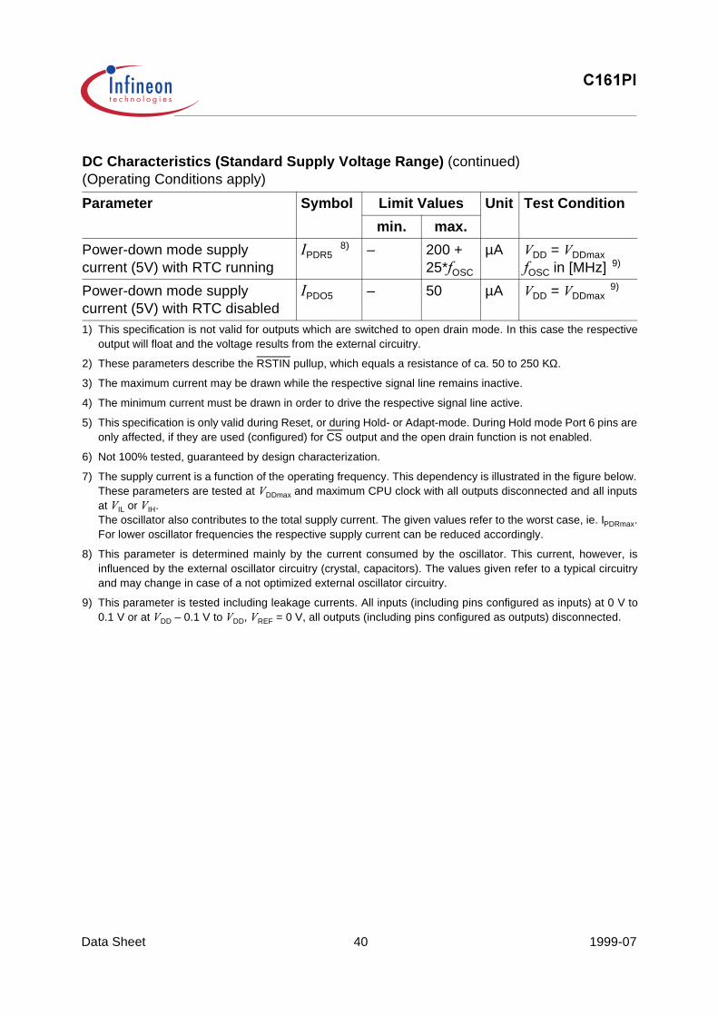
Power-down mode supply current (5V) with RTC running
,PDR5 8) – 200 +
25*IOSC
µA 9DD = 9DDmax
IOSC in [MHz] 9)
Power-down mode supply current (5V) with RTC disabled
,PDO5 – 50 µA 9DD = 9DDmax 9)
1) This specification is not valid for outputs which are switched to open drain mode. In this case the respectiveoutput will float and the voltage results from the external circuitry.
2) These parameters describe the RSTIN pullup, which equals a resistance of ca. 50 to 250 KΩ.
3) The maximum current may be drawn while the respective signal line remains inactive.
4) The minimum current must be drawn in order to drive the respective signal line active.
5) This specification is only valid during Reset, or during Hold- or Adapt-mode. During Hold mode Port 6 pins areonly affected, if they are used (configured) for CS output and the open drain function is not enabled.
6) Not 100% tested, guaranteed by design characterization.
7) The supply current is a function of the operating frequency. This dependency is illustrated in the figure below.These parameters are tested at 9DDmax and maximum CPU clock with all outputs disconnected and all inputsat 9IL or 9IH.The oscillator also contributes to the total supply current. The given values refer to the worst case, ie. IPDRmax.For lower oscillator frequencies the respective supply current can be reduced accordingly.
8) This parameter is determined mainly by the current consumed by the oscillator. This current, however, isinfluenced by the external oscillator circuitry (crystal, capacitors). The values given refer to a typical circuitryand may change in case of a not optimized external oscillator circuitry.
9) This parameter is tested including leakage currents. All inputs (including pins configured as inputs) at 0 V to0.1 V or at 9DD – 0.1 V to 9DD, 9REF = 0 V, all outputs (including pins configured as outputs) disconnected.
DC Characteristics (Standard Supply Voltage Range) (continued)(Operating Conditions apply)
Parameter Symbol Limit Values Unit Test Condition
min. max.

&3,
Data Sheet 41 1999-07
DC Characteristics (Reduced Supply Voltage Range)(Operating Conditions apply)
Parameter Symbol Limit Values Unit Test Condition
min. max.
Input low voltage XTAL1,P3.0, P3.1, P6.5, P6.6, P6.7
9IL1 SR – 0.5 0.3 VDD V –
Input low voltage(TTL)
9IL SR – 0.5 0.8 V –
Input low voltage(Special Threshold)
9ILS SR – 0.5 1.3 V –
Input high voltage RSTIN 9IH1 SR 0.6 9DD 9DD + 0.5
V –
Input high voltage XTAL1,P3.0, P3.1, P6.5, P6.6, P6.7
9IH2 SR 0.7 9DD 9DD + 0.5
V –
Input high voltage(TTL)
9IH SR 1.8 9DD + 0.5
V –
Input high voltage(Special Threshold)
9IHS SR 0.8 9DD
- 0.29DD + 0.5
V –
Input Hysteresis(Special Threshold)
HYS 250 – mV –
Output low voltage(PORT0, PORT1, Port 4, ALE, RD, WR, BHE, CLKOUT, RSTOUT)
9OL CC – 0.45 V ,OL = 1.6 mA
Output low voltageP3.0, P3.1, P6.5, P6.6, P6.7
9OL2 CC – 0.4 V ,OL2 = 1.6 mA
Output low voltage(all other outputs)
9OL1 CC – 0.45 V ,OL = 1.0 mA
Output high voltage 1)
(PORT0, PORT1, Port 4, ALE, RD, WR, BHE, CLKOUT, RSTOUT)
9OH CC 0.9 9DD – V ,OH = -0.5 mA
Output high voltage 1)
(all other outputs)9OH1 CC 0.9 9DD – V ,OH = -0.25 mA
Input leakage current (Port 5) ,OZ1 CC – ±200 nA 0.45V < 9IN < 9DD
Input leakage current (all other) ,OZ2 CC – ±500 nA 0.45V < 9IN < 9DD
RSTIN inactive current 2) ,RSTH 3) – -10 µA 9IN = 9IH1

&3,
Data Sheet 42 1999-07
RSTIN active current 2) ,RSTL 4) -100 – µA 9IN = 9IL
Read/Write inactive current 5) ,RWH 3) – -10 µA 9OUT = 2.4 V
Read/Write active current 5) ,RWL 4) -500 – µA 9OUT = 9OLmax
ALE inactive current 5) ,ALEL 3) – 20 µA 9OUT = 9OLmax
ALE active current 5) ,ALEH 4) 500 – µA 9OUT = 2.4 V
Port 6 inactive current 5) ,P6H 3) – -10 µA 9OUT = 2.4 V
Port 6 active current 5) ,P6L 4) -500 – µA 9OUT = 9OL1max
PORT0 configuration current 5) ,P0H 3) – -5 µA 9IN = 9IHmin
,P0L 4) -100 – µA 9IN = 9ILmax
XTAL1 input current ,IL CC – ±20 µA 0 V < 9IN < 9DD
Pin capacitance 6) (digital inputs/outputs)
&IO CC – 10 pF I = 1 MHz7A = 25 °C
Power supply current (3V active)with all peripherals active
,DD3 – 1 +1.1*ICPU
mA RSTIN = 9IL2 ICPU in [MHz] 7)
Idle mode supply current (3V)with all peripherals active
,IDX3 – 1 +0.5*ICPU
mA RSTIN = 9IH1
ICPU in [MHz] 7)
Idle mode supply current (3V)with all peripherals deactivated,PLL off, SDD factor = 32
,IDO3 8) – 300 +
30*IOSC
µA RSTIN = 9IH1
IOSC in [MHz] 7)
Power-down mode supplycurrent (3V) with RTC running
,PDR3 8) – 100 +
10*IOSC
µA 9DD = 9DDmax
IOSC in [MHz] 9)
Power-down mode supplycurrent (3V) with RTC disabled
,PDO3 – 30 µA 9DD = 9DDmax 9)
1) This specification is not valid for outputs which are switched to open drain mode. In this case the respectiveoutput will float and the voltage results from the external circuitry.
2) These parameters describe the RSTIN pullup, which equals a resistance of ca. 50 to 250 KΩ.
3) The maximum current may be drawn while the respective signal line remains inactive.
4) The minimum current must be drawn in order to drive the respective signal line active.
5) This specification is only valid during Reset, or during Hold- or Adapt-mode. During Hold mode Port 6 pins areonly affected, if they are used (configured) for CS output and the open drain function is not enabled.
6) Not 100% tested, guaranteed by design characterization.
DC Characteristics (continued) (Reduced Supply Voltage Range)(Operating Conditions apply)
Parameter Symbol Limit Values Unit Test Condition
min. max.

&3,
Data Sheet 43 1999-07
Figure 9 Idle and Power Down Supply Current as a Function of Oscillator Frequency
7) The supply current is a function of the operating frequency. This dependency is illustrated in the figure below.These parameters are tested at 9DDmax and maximum CPU clock with all outputs disconnected and all inputsat 9IL or 9IH.The oscillator also contributes to the total supply current. The given values refer to the worst case, ie. IPDRmax.For lower oscillator frequencies the respective supply current can be reduced accordingly.
8) This parameter is determined mainly by the current consumed by the oscillator. This current, however, isinfluenced by the external oscillator circuitry (crystal, capacitors). The values given refer to a typical circuitryand may change in case of a not optimized external oscillator circuitry.
9) This parameter is tested including leakage currents. All inputs (including pins configured as inputs) at 0 V to0.1 V or at 9DD – 0.1 V to 9DD, 9REF = 0 V, all outputs (including pins configured as outputs) disconnected.
I [µ
A]
IOSC [MHz]4
,3'5PD[
8 12 16
,3'2PD[
1500
1250
1000
750
500
250
,,'2PD[
,,'2PD[
,3'5PD[

&3,
Data Sheet 44 1999-07
Figure 10 Supply/Idle Current as a Function of Operating Frequency
, [m
A]
ICPU [MHz]5 10 15 25
50
25
5
IDD5max
IID5max
IDD5typ
IID5typ
20
IDD3max
IDD3typ
IID3max
IID3typ

&3,
Data Sheet 45 1999-07
AC CharacteristicsDefinition of Internal Timing
The internal operation of the C161PI is controlled by the internal CPU clock fCPU. Bothedges of the CPU clock can trigger internal (e.g. pipeline) or external (e.g. bus cycles)operations.
The specification of the external timing (AC Characteristics) therefore depends on thetime between two consecutive edges of the CPU clock, called “TCL” (see figure below).
Figure 11 Generation Mechanisms for the CPU Clock
The CPU clock signal ICPU can be generated from the oscillator clock signal IOSC viadifferent mechanisms. The duration of TCLs and their variation (and also the derivedexternal timing) depends on the used mechanism to generate ICPU. This influence mustbe regarded when calculating the timings for the C161PI.
Note: The example for PLL operation shown in the fig. above refers to a PLL factor of 4.
The used mechanism to generate the CPU clock is selected during reset via the logiclevels on pins P0.15-13 (P0H.7-5).
The table below associates the combinations of these three bits with the respective clockgeneration mode.
TCL TCL
TCL TCL
I&38
I26&
I&38
I26&
3KDVH/RFNHG/RRS2SHUDWLRQ
'LUHFW&ORFN'ULYH
TCL TCL
I&38
I26&
3UHVFDOHU2SHUDWLRQ

&3,
Data Sheet 46 1999-07
Prescaler Operation
When pins P0.15-13 (P0H.7-5) equal 001B during reset the CPU clock is derived fromthe internal oscillator (input clock signal) by a 2:1 prescaler.The frequency of ICPU is half the frequency of IOSC and the high and low time of ICPU (i.e.the duration of an individual TCL) is defined by the period of the input clock IOSC.
The timings listed in the AC Characteristics that refer to TCLs therefore can becalculated using the period of IOSC for any TCL.
Phase Locked Loop
For all combinations of pins P0.15-13 (P0H.7-5) except for 001B and 011B the on-chipphase locked loop is enabled and provides the CPU clock (see table above). The PLLmultiplies the input frequency by the factor F which is selected via the combination ofpins P0.15-13 (i.e. ICPU = IOSC * F). With every F’th transition of IOSC the PLL circuitsynchronizes the CPU clock to the input clock. This synchronization is done smoothly,i.e. the CPU clock frequency does not change abruptly.
Due to this adaptation to the input clock the frequency of ICPU is constantly adjusted soit is locked to IOSC. The slight variation causes a jitter of ICPU which also effects theduration of individual TCLs.
Table 8 C161PI Clock Generation Modes
P0.15-13(P0H.7-5)
CPU Frequency ICPU = IOSC * F
External Clock Input Range 1)
Notes
1 1 1 IOSC * 4 2.5 to 6.25 MHz Default configuration
1 1 0 IOSC * 3 3.33 to 8.33 MHz
1 0 1 IOSC * 2 5 to 12.5 MHz
1 0 0 IOSC * 5 2 to 5 MHz
0 1 1 IOSC * 1 1 to 25 MHz Direct drive 2)
0 1 0 IOSC * 1.5 6.66 to 16.6 MHz
0 0 1 IOSC / 2 2 to 50 MHz CPU clock via prescaler
0 0 0 IOSC * 2.5 4 to 10 MHz1) The external clock input range refers to a CPU clock range of 10...25 MHz.
2) The maximum frequency depends on the duty cycle of the external clock signal.

&3,
Data Sheet 47 1999-07
The timings listed in the AC Characteristics that refer to TCLs therefore must becalculated using the minimum TCL that is possible under the respective circumstances.
The actual minimum value for TCL depends on the jitter of the PLL. As the PLL isconstantly adjusting its output frequency so it corresponds to the applied input frequency(crystal or oscillator) the relative deviation for periods of more than one TCL is lower thanfor one single TCL (see formula and figure below).For a period of N * TCL the minimum value is computed using the correspondingdeviation DN:
(N * TCL)min = N * TCLNOM - DN DN [ns] = ±(13.3 + N*6.3) / ICPU [MHz],where N = number of consecutive TCLs and 1 ≤ N ≤ 40.
So for a period of 3 TCLs @ 25 MHz (i.e. N = 3): D3 = (13.3 + 3 * 6.3) / 25 = 1.288 ns,and (3TCL)min = 3TCLNOM - 1.288 ns = 58.7 ns (@ ICPU = 25 MHz).
This is especially important for bus cycles using waitstates and e.g. for the operation oftimers, serial interfaces, etc. For all slower operations and longer periods (e.g. pulse traingeneration or measurement, lower baudrates, etc.) the deviation caused by the PLL jitteris neglectible.
Note: For all periods longer than 40 TCL the N=40 value can be used (see figure below).
Figure 12 Approximated Maximum Accumulated PLL Jitter
40201051
±1
±10
±20
N
This approximated formula is valid for 1 ≤ 1 ≤ 40 and 10MHz ≤ fCPU ≤ 25MHz.
±26.5
Max.jitter D1 [ns]
20 MHz
25 MHz
16 MHz
10 MHz

&3,
Data Sheet 48 1999-07
Direct Drive
When pins P0.15-13 (P0H.7-5) equal 011B during reset the on-chip phase locked loop isdisabled and the CPU clock is directly driven from the internal oscillator with the inputclock signal.The frequency of ICPU directly follows the frequency of IOSC so the high and low time ofICPU (i.e. the duration of an individual TCL) is defined by the duty cycle of the input clockIOSC.
The timings listed below that refer to TCLs therefore must be calculated using theminimum TCL that is possible under the respective circumstances. This minimum valuecan be calculated via the following formula:
TCLmin = 1/IOSC * DCmin (DC = duty cycle)
For two consecutive TCLs the deviation caused by the duty cycle of IOSC is compensatedso the duration of 2TCL is always 1/IOSC. The minimum value TCLmin therefore has to beused only once for timings that require an odd number of TCLs (1,3,...). Timings thatrequire an even number of TCLs (2,4,...) may use the formula 2TCL = 1/IOSC.
Note: The address float timings in Multiplexed bus mode (W11 and W45) use the maximumduration of TCL (TCLmax = 1/IOSC * DCmax) instead of TCLmin.
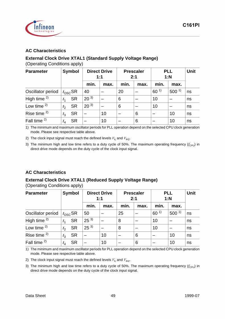
&3,
Data Sheet 49 1999-07
AC Characteristics
AC Characteristics
External Clock Drive XTAL1 (Standard Supply Voltage Range)(Operating Conditions apply)
Parameter Symbol Direct Drive1:1
Prescaler2:1
PLL1:N
Unit
min. max. min. max. min. max.
Oscillator period WOSCSR 40 – 20 – 60 1)
1) The minimum and maximum oscillator periods for PLL operation depend on the selected CPU clock generationmode. Please see respective table above.
500 1) ns
High time 2)
2) The clock input signal must reach the defined levels 9IL and 9IH2.
W1 SR 20 3)
3) The minimum high and low time refers to a duty cycle of 50%. The maximum operating frequency (ICPU) indirect drive mode depends on the duty cycle of the clock input signal.
– 6 – 10 – ns
Low time 2) W2 SR 20 3) – 6 – 10 – ns
Rise time 2) W3 SR – 10 – 6 – 10 ns
Fall time 2) W4 SR – 10 – 6 – 10 ns
External Clock Drive XTAL1 (Reduced Supply Voltage Range)(Operating Conditions apply)
Parameter Symbol Direct Drive1:1
Prescaler2:1
PLL1:N
Unit
min. max. min. max. min. max.
Oscillator period WOSCSR 50 – 25 – 60 1)
1) The minimum and maximum oscillator periods for PLL operation depend on the selected CPU clock generationmode. Please see respective table above.
500 1) ns
High time 2)
2) The clock input signal must reach the defined levels 9IL and 9IH2.
W1 SR 25 3)
3) The minimum high and low time refers to a duty cycle of 50%. The maximum operating frequency (ICPU) indirect drive mode depends on the duty cycle of the clock input signal.
– 8 – 10 – ns
Low time 2) W2 SR 25 3) – 8 – 10 – ns
Rise time 2) W3 SR – 10 – 6 – 10 ns
Fall time 2) W4 SR – 10 – 6 – 10 ns

&3,
Data Sheet 50 1999-07
Figure 13 External Clock Drive XTAL1
Note: The main oscillator is optimized for oscillation with a crystal within a frequencyrange of 4...16 MHz. When driven by an external clock signal it will accept thespecified frequency range. Operation at lower input frequencies is possible but isguaranteed by design only (not 100% tested).It is strongly recommended to measure the oscillation allowance (or margin) in thefinal target system (layout) to determine the optimum parameters for the oscillatoroperation.

&3,
Data Sheet 51 1999-07
A/D Converter Characteristics(Operating Conditions apply)4.0V (2.6V)≤9AREF ≤ 9DD + 0.1V (Note the influence on TUE.)9SS - 0.1V ≤ 9AGND ≤ 9SS + 0.2V
Parameter Symbol Limit Values Unit Test Condition
min. max.
Analog input voltage range 9AIN SR 9AGND 9AREF V 1)
1) 9AIN may exceed 9AGND or 9AREF up to the absolute maximum ratings. However, the conversion result in thesecases will be X000H or X3FFH, respectively.
Basic clock frequency IBC 0.5 6.25 MHz 2)
2) The limit values for IBC must not be exceeded when selecting the CPU frequency and the ADCTC setting.
Conversion time WC CC – 40 WBC + WS+2WCPU
3)
WCPU = 1 / ICPU
3) This parameter includes the sample time WS, the time for determining the digital result and the time to load theresult register with the conversion result.Values for the basic clock WBC depend on the conversion time programming.This parameter depends on the ADC control logic. It is not a real maximum value, but rather a fixum.
Total unadjusted error TUE CC4)
4) TUE is tested at 9AREF=5.0V (3.3V), 9AGND=0V, 9DD=4.9V (3.2V). It is guaranteed by design for all othervoltages within the defined voltage range.The specified TUE is guaranteed only if an overload condition (see ,OV specification) occurs on maximum 2 notselected analog input pins and the absolute sum of input overload currents on all analog input pins does notexceed 10 mA.During the reset calibration sequence the maximum TUE may be ±4 LSB (±8 LSB @ 3V).
– ± 2 LSB 9AREF ≥ 4.0 V 5)
5) This case is not applicable for the reduced supply voltage range.
– ± 4 LSB 9AREF ≥ 2.6 V
Internal resistance of reference voltage source
5AREF SR – WBC / 60- 0.25
kΩ WBC in [ns] 6) 7)
6) During the conversion the ADC’s capacitance must be repeatedly charged or discharged. The internalresistance of the reference voltage source must allow the capacitance to reach its respective voltage levelwithin each conversion step. The maximum internal resistance results from the programmed conversion timing.
7) Not 100% tested, guaranteed by design.
Internal resistance of analog source
5ASRC SR – WS / 450- 0.25
kΩ WS in [ns] 7) 8)
8) During the sample time the input capacitance &I can be charged/discharged by the external source. Theinternal resistance of the analog source must allow the capacitance to reach its final voltage level within WS.After the end of the sample time WS, changes of the analog input voltage have no effect on the conversion result.Values for the sample time WS depend on programming and can be taken from the table below.
ADC input capacitance &AIN CC – 33 pF 7)

&3,
Data Sheet 52 1999-07
Sample time and conversion time of the C161PI’s A/D Converter are programmable. Thetable below should be used to calculate the above timings.The limit values for IBC must not be exceeded when selecting ADCTC.
Converter Timing Example:
Assumptions: ICPU = 25 MHz (i.e. WCPU = 40 ns), ADCTC = ’00’, ADSTC = ’00’.
Basic clock IBC = ICPU / 4 = 6.25 MHz, i.e. WBC = 160 ns.Sample time WS = WBC * 8 = 1280 ns.Conversion time WC = WS + 40 WBC + 2 WCPU = (1280 + 6400 + 80) ns = 7.8 µs.
Memory Cycle Variables
The timing tables below use three variables which are derived from the BUSCONxregisters and represent the special characteristics of the programmed memory cycle.The following table describes, how these variables are to be computed.
Table 9 A/D Converter Computation Table
ADCON.15|14(ADCTC)
A/D ConverterBasic clock IBC
ADCON.13|12(ADSTC)
Sample timeWS
00 ICPU / 4 00 WBC * 8
01 ICPU / 2 01 WBC * 16
10 ICPU / 16 10 WBC * 32
11 ICPU / 8 11 WBC * 64
Table 10 Memory Cycle Variables
Description Symbol Values
ALE Extension WA TCL * <ALECTL>
Memory Cycle Time Waitstates WC 2TCL * (15 - <MCTC>)
Memory Tristate Time WF 2TCL * (1 - <MTTC>)

&3,
Data Sheet 53 1999-07
Testing Waveforms
Figure 14 Input Output Waveforms
Figure 15 Float Waveforms
AC inputs during testing are driven at 2.4 V for a logic ‘1’ and 0.45 V for a logic ‘0’.Timing measurements are made at 9IH min for a logic ’1’ and 9IL max for a logic ’0’.
2.4 V
0.45 V
Test Points
1.8 V 1.8 V
0.8 V 0.8 V
For timing purposes a port pin is no longer floating when a 100 mV change from load voltage occurs,but begins to float when a 100 mV change from the loaded 9OH/9OL level occurs (,OH/,OL = 20 mA).

&3,
Data Sheet 54 1999-07
AC Characteristics
Multiplexed Bus (Standard Supply Voltage Range)(Operating Conditions apply)ALE cycle time = 6 TCL + 2WA + WC + WF (120 ns at 25 MHz CPU clock without waitstates)
Parameter Symbol Max. CPU Clock= 25 MHz
Variable CPU Clock1 / 2TCL = 1 to 25 MHz
Unit
min. max. min. max.
ALE high time W5 CC 10 + WA – TCL - 10 +WA
– ns
Address setup to ALE W6 CC 4 +WA – TCL - 16 +WA
– ns
Address hold after ALE W7 CC 10 +WA – TCL - 10 +WA
– ns
ALE falling edge to RD, WR (with RW-delay)
W8 CC 10 +WA – TCL - 10 +WA
– ns
ALE falling edge to RD, WR (no RW-delay)
W9 CC -10 +WA – -10 +WA – ns
Address float after RD, WR (with RW-delay)
W10 CC – 6 – 6 ns
Address float after RD, WR (no RW-delay)
W11 CC – 26 – TCL + 6 ns
RD, WR low time(with RW-delay)
W12 CC 30 +WC – 2TCL - 10+WC
– ns
RD, WR low time (no RW-delay)
W13 CC 50 +WC – 3TCL-10+WC
– ns
RD to valid data in (with RW-delay)
W14 SR – 20 +WC – 2TCL - 20+WC
ns
RD to valid data in (no RW-delay)
W15 SR – 40 +WC – 3TCL - 20+WC
ns
ALE low to valid data in W16 SR – 40 + WA
+ WC– 3TCL - 20
+WA +WCns
Address to valid data in W17 SR – 50 + 2WA
+ WC– 4TCL - 30
+2WA +WCns
Data hold after RDrising edge
W18 SR 0 – 0 – ns
Data float after RD W19 SR – 26 +WF – 2TCL - 14 +WF
ns

&3,
Data Sheet 55 1999-07
Data valid to WR W22 CC 20 +WC – 2TCL - 20+WC
– ns
Data hold after WR W23 CC 26 +WF – 2TCL - 14+WF
– ns
ALE rising edge after RD, WR
W25 CC 26 +WF – 2TCL - 14 +WF
– ns
Address hold after RD, WR
W27 CC 26 +WF – 2TCL - 14 +WF
– ns
ALE falling edge to CS 1) W38 CC -4 -WA 10 - WA -4 -WA 10 -WA ns
CS low to Valid Data In 1) W39 SR – 40+WC+2WA
– 3TCL - 20+WC + 2WA
ns
CS hold after RD, WR 1) W40 CC 46 +WF – 3TCL - 14 +WF
– ns
ALE fall. edge to RdCS, WrCS (with RW delay)
W42 CC 16 +WA – TCL - 4+WA
– ns
ALE fall. edge to RdCS, WrCS (no RW delay)
W43 CC -4 +WA – -4+WA
– ns
Address float after RdCS, WrCS (with RW delay)
W44 CC – 0 – 0 ns
Address float after RdCS, WrCS (no RW delay)
W45 CC – 20 – TCL ns
RdCS to Valid Data In(with RW delay)
W46 SR – 16 +WC – 2TCL - 24+WC
ns
RdCS to Valid Data In(no RW delay)
W47 SR – 36 +WC – 3TCL - 24+WC
ns
RdCS, WrCS Low Time(with RW delay)
W48 CC 30 +WC – 2TCL - 10+WC
– ns
RdCS, WrCS Low Time(no RW delay)
W49 CC 50 +WC – 3TCL - 10+WC
– ns
Multiplexed Bus (Standard Supply Voltage Range) (continued)(Operating Conditions apply)ALE cycle time = 6 TCL + 2WA + WC + WF (120 ns at 25 MHz CPU clock without waitstates)
Parameter Symbol Max. CPU Clock= 25 MHz
Variable CPU Clock1 / 2TCL = 1 to 25 MHz
Unit
min. max. min. max.

&3,
Data Sheet 56 1999-07
Data valid to WrCS W50 CC 26 +WC – 2TCL - 14+WC
– ns
Data hold after RdCS W51 SR 0 – 0 – ns
Data float after RdCS W52 SR – 20 +WF – 2TCL - 20 +WF
ns
Address hold afterRdCS, WrCS
W54 CC 20 +WF – 2TCL - 20 +WF
– ns
Data hold after WrCS W56 CC 20 +WF – 2TCL - 20 +WF
– ns
1) These parameters refer to the latched chip select signals (CSxL). The early chip select signals (CSxE) arespecified together with the address and signal BHE (see figures below).
Multiplexed Bus (Standard Supply Voltage Range) (continued)(Operating Conditions apply)ALE cycle time = 6 TCL + 2WA + WC + WF (120 ns at 25 MHz CPU clock without waitstates)
Parameter Symbol Max. CPU Clock= 25 MHz
Variable CPU Clock1 / 2TCL = 1 to 25 MHz
Unit
min. max. min. max.
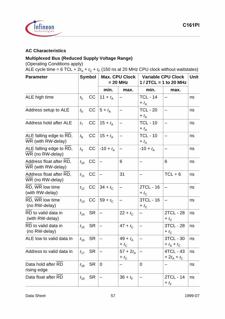
&3,
Data Sheet 57 1999-07
AC Characteristics
Multiplexed Bus (Reduced Supply Voltage Range)(Operating Conditions apply)ALE cycle time = 6 TCL + 2WA + WC + WF (150 ns at 20 MHz CPU clock without waitstates)
Parameter Symbol Max. CPU Clock= 20 MHz
Variable CPU Clock1 / 2TCL = 1 to 20 MHz
Unit
min. max. min. max.
ALE high time W5 CC 11 + WA – TCL - 14+WA
– ns
Address setup to ALE W6 CC 5 +WA – TCL - 20+WA
– ns
Address hold after ALE W7 CC 15 +WA – TCL - 10+WA
– ns
ALE falling edge to RD, WR (with RW-delay)
W8 CC 15 +WA – TCL - 10+WA
– ns
ALE falling edge to RD, WR (no RW-delay)
W9 CC -10 +WA – -10 +WA – ns
Address float after RD, WR (with RW-delay)
W10 CC – 6 – 6 ns
Address float after RD, WR (no RW-delay)
W11 CC – 31 – TCL + 6 ns
RD, WR low time(with RW-delay)
W12 CC 34 +WC – 2TCL - 16+WC
– ns
RD, WR low time (no RW-delay)
W13 CC 59 +WC – 3TCL - 16+ WC
– ns
RD to valid data in (with RW-delay)
W14 SR – 22 +WC – 2TCL - 28+WC
ns
RD to valid data in (no RW-delay)
W15 SR – 47 +WC – 3TCL - 28+WC
ns
ALE low to valid data in W16 SR – 49 + WA
+ WC– 3TCL - 30
+WA +WCns
Address to valid data in W17 SR – 57 + 2WA
+ WC– 4TCL - 43
+2WA +WCns
Data hold after RDrising edge
W18 SR 0 – 0 – ns
Data float after RD W19 SR – 36 +WF – 2TCL - 14 +WF
ns
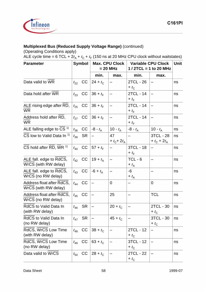
&3,
Data Sheet 58 1999-07
Data valid to WR W22 CC 24 +WC – 2TCL - 26+WC
– ns
Data hold after WR W23 CC 36 +WF – 2TCL - 14+WF
– ns
ALE rising edge after RD, WR
W25 CC 36 +WF – 2TCL - 14 +WF
– ns
Address hold after RD, WR
W27 CC 36 +WF – 2TCL - 14 +WF
– ns
ALE falling edge to CS 1) W38 CC -8 -WA 10 - WA -8 -WA 10 -WA ns
CS low to Valid Data In 1) W39 SR – 47+WC+2WA
– 3TCL - 28+WC + 2WA
ns
CS hold after RD, WR 1) W40 CC 57 +WF – 3TCL - 18+ WF
– ns
ALE fall. edge to RdCS, WrCS (with RW delay)
W42 CC 19 +WA – TCL - 6+WA
– ns
ALE fall. edge to RdCS, WrCS (no RW delay)
W43 CC -6 +WA – -6+WA
– ns
Address float after RdCS, WrCS (with RW delay)
W44 CC – 0 – 0 ns
Address float after RdCS, WrCS (no RW delay)
W45 CC – 25 – TCL ns
RdCS to Valid Data In(with RW delay)
W46 SR – 20 +WC – 2TCL - 30+WC
ns
RdCS to Valid Data In(no RW delay)
W47 SR – 45 +WC – 3TCL - 30+WC
ns
RdCS, WrCS Low Time(with RW delay)
W48 CC 38 +WC – 2TCL - 12+WC
– ns
RdCS, WrCS Low Time(no RW delay)
W49 CC 63 +WC – 3TCL - 12+WC
– ns
Data valid to WrCS W50 CC 28 +WC – 2TCL - 22+WC
– ns
Multiplexed Bus (Reduced Supply Voltage Range) (continued)(Operating Conditions apply)ALE cycle time = 6 TCL + 2WA + WC + WF (150 ns at 20 MHz CPU clock without waitstates)
Parameter Symbol Max. CPU Clock= 20 MHz
Variable CPU Clock1 / 2TCL = 1 to 20 MHz
Unit
min. max. min. max.

&3,
Data Sheet 59 1999-07
Data hold after RdCS W51 SR 0 – 0 – ns
Data float after RdCS W52 SR – 30 +WF – 2TCL - 20 +WF
ns
Address hold afterRdCS, WrCS
W54 CC 30 +WF – 2TCL - 20 +WF
– ns
Data hold after WrCS W56 CC 30 +WF – 2TCL - 20 +WF
– ns
1) These parameters refer to the latched chip select signals (CSxL). The early chip select signals (CSxE) arespecified together with the address and signal BHE (see figures below).
Multiplexed Bus (Reduced Supply Voltage Range) (continued)(Operating Conditions apply)ALE cycle time = 6 TCL + 2WA + WC + WF (150 ns at 20 MHz CPU clock without waitstates)
Parameter Symbol Max. CPU Clock= 20 MHz
Variable CPU Clock1 / 2TCL = 1 to 20 MHz
Unit
min. max. min. max.

&3,
Data Sheet 60 1999-07
Figure 16 External Memory Cycle:Multiplexed Bus, With Read/Write Delay, Normal ALE
A22-A16(A15-A8)
BHE, CSxE
Data In
Data OutAddress
Address
W38
W44
W10
Address
ALE
CSxL
BUS
5HDG&\FOH
RD
RdCSx
BUS
:ULWH&\FOH
WR,WRL,WRH
WrCSx
W5 W16
W17
W6 W7
W39 W40
W25
W27
W18
W19
W14
W46
W12
W48
W10 W22
W23
W44
W12
W48
W8
W42
W42
W8
W50
W51
W54
W52
W56

&3,
Data Sheet 61 1999-07
Figure 17 External Memory Cycle:Multiplexed Bus, With Read/Write Delay, Extended ALE
Data OutAddress
Data InAddress
W38
W44
W10
Address
ALE
CSxL
A22-A16(A15-A8)
BHE, CSxE
BUS
5HDG&\FOH
RD
RdCSx
BUS
:ULWH&\FOH
WR,WRL,WRH
WrCSx
W5 W16
W17
W6 W7
W39 W40
W25
W27
W18
W19
W14
W46
W12
W48
W10 W22
W23
W44
W12
W48
W8
W42
W42
W8
W50
W51
W54
W52
W56

&3,
Data Sheet 62 1999-07
Figure 18 External Memory Cycle:Multiplexed Bus, No Read/Write Delay, Normal ALE
Data OutAddress
Address Data In
W38
Address
ALE
CSxL
A22-A16(A15-A8)
BHE, CSxE
BUS
5HDG&\FOH
RD
RdCSx
BUS
:ULWH&\FOH
WR,WRL,WRH
WrCSx
W5 W16
W17
W6 W7
W39 W40
W25
W27
W18
W19
W15
W47
W13
W49
W22
W23
W13
W49
W9
W43
W43
W9 W11
W45
W11
W45 W50
W51
W54
W52
W56
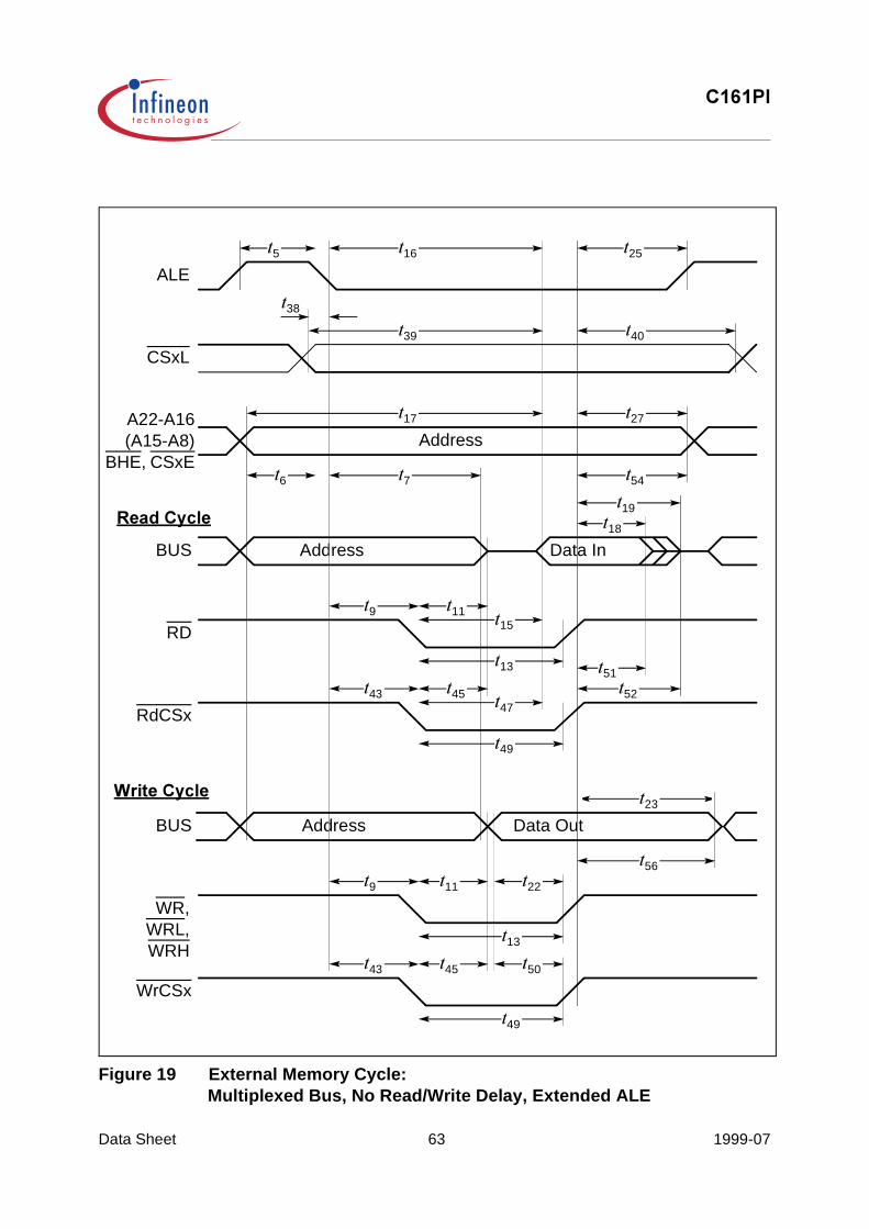
&3,
Data Sheet 63 1999-07
Figure 19 External Memory Cycle:Multiplexed Bus, No Read/Write Delay, Extended ALE
Data OutAddress
Data InAddress
W38
Address
ALE
CSxL
A22-A16(A15-A8)
BHE, CSxE
BUS
5HDG&\FOH
RD
RdCSx
BUS
:ULWH&\FOH
WR,WRL,WRH
WrCSx
W5 W16
W17
W6 W7
W39 W40
W25
W27
W18
W19
W15
W47
W13
W49
W22
W23
W13
W49
W9
W43
W43
W9 W11
W45
W11
W45 W50
W51
W54
W52
W56

&3,
Data Sheet 64 1999-07
AC Characteristics
Demultiplexed Bus (Standard Supply Voltage Range)(Operating Conditions apply)ALE cycle time = 4 TCL + 2WA + WC + WF (80 ns at 25 MHz CPU clock without waitstates)
Parameter Symbol Max. CPU Clock= 25 MHz
Variable CPU Clock1 / 2TCL = 1 to 25 MHz
Unit
min. max. min. max.
ALE high time W5 CC 10 +WA – TCL - 10+WA
– ns
Address setup to ALE W6 CC 4 +WA – TCL - 16+WA
– ns
ALE falling edge to RD, WR (with RW-delay)
W8 CC 10 +WA – TCL - 10+WA
– ns
ALE falling edge to RD, WR (no RW-delay)
W9 CC -10 +WA – -10+WA
– ns
RD, WR low time (with RW-delay)
W12 CC 30 +WC – 2TCL - 10+WC
– ns
RD, WR low time (no RW-delay)
W13 CC 50 +WC – 3TCL - 10+WC
– ns
RD to valid data in (with RW-delay)
W14 SR – 20 +WC – 2TCL - 20+WC
ns
RD to valid data in (no RW-delay)
W15 SR – 40 +WC – 3TCL - 20+WC
ns
ALE low to valid data in W16 SR – 40 +WA +WC
– 3TCL - 20+WA +WC
ns
Address to valid data in W17 SR – 50 +2WA +WC
– 4TCL - 30+2WA +WC
ns
Data hold after RDrising edge
W18 SR 0 – 0 – ns
Data float after RD rising edge (with RW-delay 1))
W20 SR – 26 +2WA +WF 1)
– 2TCL - 14+22WA +WF 1)
ns
Data float after RD rising edge (no RW-delay 1))
W21 SR – 10 +2WA +WF 1)
– TCL - 10+22WA +WF 1)
ns
Data valid to WR W22 CC 20 +WC – 2TCL - 20+WC
– ns

&3,
Data Sheet 65 1999-07
Data hold after WR W24 CC 10 +WF – TCL - 10 +WF
– ns
ALE rising edge after RD, WR
W26 CC -10 +WF – -10 +WF – ns
Address hold after WR 2) W28 CC 0 +WF – 0 +WF – ns
ALE falling edge to CS 3) W38 CC -4 -WA 10 -WA -4 -WA 10 -WA ns
CS low to Valid Data In 3) W39 SR – 40 +WC+2WA
– 3TCL - 20+WC + 2WA
ns
CS hold after RD, WR 3) W41 CC 6 +WF – TCL - 14+WF
– ns
ALE falling edge to RdCS, WrCS (with RW-delay)
W42 CC 16 +WA – TCL - 4+WA
– ns
ALE falling edge to RdCS, WrCS (no RW-delay)
W43 CC -4 +WA – -4+WA
– ns
RdCS to Valid Data In(with RW-delay)
W46 SR – 16 +WC – 2TCL - 24+WC
ns
RdCS to Valid Data In(no RW-delay)
W47 SR – 36 +WC – 3TCL - 24+WC
ns
RdCS, WrCS Low Time(with RW-delay)
W48 CC 30 +WC – 2TCL - 10+WC
– ns
RdCS, WrCS Low Time(no RW-delay)
W49 CC 50 +WC – 3TCL - 10+WC
– ns
Data valid to WrCS W50 CC 26 +WC – 2TCL - 14+WC
– ns
Data hold after RdCS W51 SR 0 – 0 – ns
Data float after RdCS(with RW-delay) 1)
W53 SR – 20 +WF – 2TCL - 20+2WA +WF 1)
ns
Data float after RdCS(no RW-delay) 1)
W68 SR – 0 +WF – TCL - 20+2WA +WF 1)
ns
Demultiplexed Bus (Standard Supply Voltage Range) (continued)(Operating Conditions apply)ALE cycle time = 4 TCL + 2WA + WC + WF (80 ns at 25 MHz CPU clock without waitstates)
Parameter Symbol Max. CPU Clock= 25 MHz
Variable CPU Clock1 / 2TCL = 1 to 25 MHz
Unit
min. max. min. max.

&3,
Data Sheet 66 1999-07
Address hold afterRdCS, WrCS
W55 CC -6 +WF – -6 +WF – ns
Data hold after WrCS W57 CC 6 +WF – TCL - 14 +WF
– ns
1) RW-delay and WA refer to the next following bus cycle (including an access to an on-chip X-Peripheral).
2) Read data are latched with the same clock edge that triggers the address change and the rising RD edge.Therefore address changes before the end of RD have no impact on read cycles.
3) These parameters refer to the latched chip select signals (CSxL). The early chip select signals (CSxE) arespecified together with the address and signal BHE (see figures below).
Demultiplexed Bus (Standard Supply Voltage Range) (continued)(Operating Conditions apply)ALE cycle time = 4 TCL + 2WA + WC + WF (80 ns at 25 MHz CPU clock without waitstates)
Parameter Symbol Max. CPU Clock= 25 MHz
Variable CPU Clock1 / 2TCL = 1 to 25 MHz
Unit
min. max. min. max.

&3,
Data Sheet 67 1999-07
AC Characteristics
Demultiplexed Bus (Reduced Supply Voltage Range)(Operating Conditions apply)ALE cycle time = 4 TCL + 2WA + WC + WF (100 ns at 20 MHz CPU clock without waitstates)
Parameter Symbol Max. CPU Clock= 20 MHz
Variable CPU Clock1 / 2TCL = 1 to 20 MHz
Unit
min. max. min. max.
ALE high time W5 CC 11 +WA – TCL - 14+WA
– ns
Address setup to ALE W6 CC 5 +WA – TCL - 20+WA
– ns
ALE falling edge to RD, WR (with RW-delay)
W8 CC 15 +WA – TCL - 10+WA
– ns
ALE falling edge to RD, WR (no RW-delay)
W9 CC -10 +WA – -10+WA
– ns
RD, WR low time (with RW-delay)
W12 CC 34 +WC – 2TCL - 16+WC
– ns
RD, WR low time (no RW-delay)
W13 CC 59 +WC – 3TCL - 16+WC
– ns
RD to valid data in (with RW-delay)
W14 SR – 22 +WC – 2TCL - 28+WC
ns
RD to valid data in (no RW-delay)
W15 SR – 47 +WC – 3TCL - 28+WC
ns
ALE low to valid data in W16 SR – 49 +WA +WC
– 3TCL - 30+WA +WC
ns
Address to valid data in W17 SR – 57 +2WA +WC
– 4TCL - 43+2WA +WC
ns
Data hold after RDrising edge
W18 SR 0 – 0 – ns
Data float after RD rising edge (with RW-delay 1))
W20 SR – 36 +2WA +WF 1)
– 2TCL - 14+2WA +WF 1)
ns
Data float after RD rising edge (no RW-delay 1))
W21 SR – 15 +2WA +WF 1)
– TCL - 10+2WA +WF 1)
ns
Data valid to WR W22 CC 24 +WC – 2TCL - 26+WC
– ns

&3,
Data Sheet 68 1999-07
Data hold after WR W24 CC 15 +WF – TCL - 10+WF
– ns
ALE rising edge after RD, WR
W26 CC -12 +WF – -12 +WF – ns
Address hold after WR 2) W28 CC 0 +WF – 0 +WF – ns
ALE falling edge to CS 3) W38 CC -8 -WA 10 -WA -8 -WA 10 -WA ns
CS low to Valid Data In 3) W39 SR – 47 +WC+2WA
– 3TCL - 28+WC + 2WA
ns
CS hold after RD, WR 3) W41 CC 9 +WF – TCL - 16+WF
– ns
ALE falling edge to RdCS, WrCS (with RW-delay)
W42 CC 19 +WA – TCL - 6+WA
– ns
ALE falling edge to RdCS, WrCS (no RW-delay)
W43 CC -6 +WA – -6+WA
– ns
RdCS to Valid Data In(with RW-delay)
W46 SR – 20 +WC – 2TCL - 30+WC
ns
RdCS to Valid Data In(no RW-delay)
W47 SR – 45 +WC – 3TCL - 30+WC
ns
RdCS, WrCS Low Time(with RW-delay)
W48 CC 38 +WC – 2TCL - 12+WC
– ns
RdCS, WrCS Low Time(no RW-delay)
W49 CC 63 +WC – 3TCL - 12+WC
– ns
Data valid to WrCS W50 CC 28 +WC – 2TCL - 22+WC
– ns
Data hold after RdCS W51 SR 0 – 0 – ns
Data float after RdCS(with RW-delay) 1)
W53 SR – 30 +WF – 2TCL - 20+2WA +WF 1)
ns
Data float after RdCS(no RW-delay) 1)
W68 SR – 5 +WF – TCL - 20+2WA +WF 1)
ns
Demultiplexed Bus (Reduced Supply Voltage Range) (continued)(Operating Conditions apply)ALE cycle time = 4 TCL + 2WA + WC + WF (100 ns at 20 MHz CPU clock without waitstates)
Parameter Symbol Max. CPU Clock= 20 MHz
Variable CPU Clock1 / 2TCL = 1 to 20 MHz
Unit
min. max. min. max.

&3,
Data Sheet 69 1999-07
Address hold afterRdCS, WrCS
W55 CC -16 +WF – -16 +WF – ns
Data hold after WrCS W57 CC 9 +WF – TCL - 16+WF
– ns
1) RW-delay and WA refer to the next following bus cycle (including an access to an on-chip X-Peripheral).
2) Read data are latched with the same clock edge that triggers the address change and the rising RD edge.Therefore address changes before the end of RD have no impact on read cycles.
3) These parameters refer to the latched chip select signals (CSxL). The early chip select signals (CSxE) arespecified together with the address and signal BHE (see figures below).
Demultiplexed Bus (Reduced Supply Voltage Range) (continued)(Operating Conditions apply)ALE cycle time = 4 TCL + 2WA + WC + WF (100 ns at 20 MHz CPU clock without waitstates)
Parameter Symbol Max. CPU Clock= 20 MHz
Variable CPU Clock1 / 2TCL = 1 to 20 MHz
Unit
min. max. min. max.

&3,
Data Sheet 70 1999-07
Figure 20 External Memory Cycle:Demultiplexed Bus, With Read/Write Delay, Normal ALE
Data Out
Data In
W38
Address
ALE
CSxL
A22-A16A15-A0
BHE, CSxE
BUS(D15-D8)
D7-D0
5HDG&\FOH
RD
RdCSx
:ULWH&\FOH
WrCSx
W5 W16
W17
W6
W39 W41
W26
W28
W18
W20
W14
W46
W12
W48
W22
W24
W12
W48
W8
W42
W42
W8
W50
W51
W55
W53
W57
BUS(D15-D8)
D7-D0
WR,WRL,WRH

&3,
Data Sheet 71 1999-07
Figure 21 External Memory Cycle:Demultiplexed Bus, With Read/Write Delay, Extended ALE
Data Out
Data In
W38
Address
ALE
CSxL
A22-A16A15-A0
BHE,CSxE
5HDG&\FOH
RD
RdCSx
:ULWH&\FOH
WrCSx
W5 W16
W17
W6
W39 W41
W26
W28
W18
W20
W14
W46
W12
W48
W22
W24
W12
W48
W8
W42
W42
W8
W50
W51
W55
W53
W57
BUS(D15-D8)
D7-D0
BUS(D15-D8)
D7-D0
WR,WRL,WRH

&3,
Data Sheet 72 1999-07
Figure 22 External Memory Cycle:Demultiplexed Bus, No Read/Write Delay, Normal ALE
Data Out
Data In
W38
Address
ALE
CSxL
A22-A16A15-A0
BHE, CSxE
5HDG&\FOH
RD
RdCSx
:ULWH&\FOH
WrCSx
W5 W16
W17
W6
W39 W41
W26
W28
W18
W21
W15
W47
W13
W49
W22
W24
W13
W49
W9
W43
W43
W9
W50
W51
W55
W68
W57
BUS(D15-D8)
D7-D0
BUS(D15-D8)
D7-D0
WR,WRL,WRH

&3,
Data Sheet 73 1999-07
Figure 23 External Memory Cycle:Demultiplexed Bus, No Read/Write Delay, Extended ALE
Data Out
Data In
W38
Address
ALE
CSxL
A22-A16A15-A0
BHE,CSxE
5HDG&\FOH
RD
RdCSx
:ULWH&\FOH
WR,WRL, WRH
WrCSx
W5 W16
W17
W6
W39 W41
W26
W28
W18
W21
W15
W47
W13
W49
W22
W24
W13
W49
W9
W43
W43
W9
W50
W51
W55
W68
W57
BUS(D15-D8)
D7-D0
BUS(D15-D8)
D7-D0
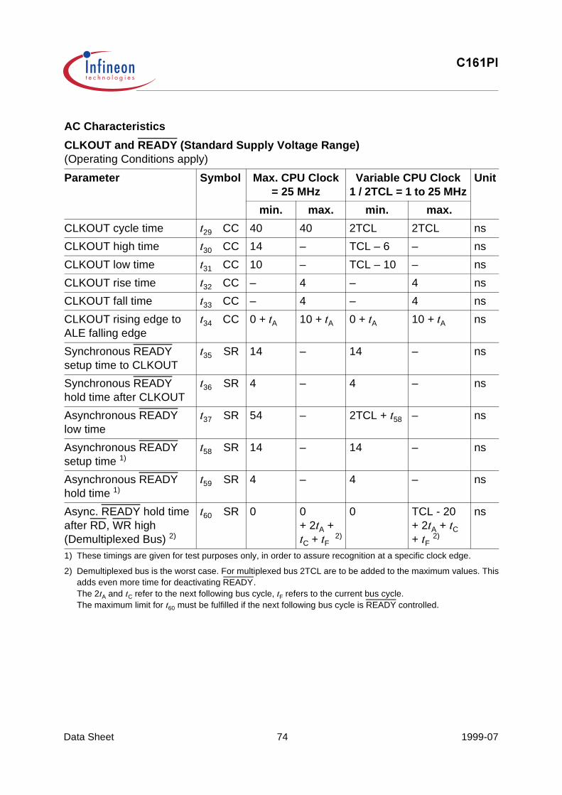
&3,
Data Sheet 74 1999-07
AC Characteristics
CLKOUT and READY (Standard Supply Voltage Range)(Operating Conditions apply)
Parameter Symbol Max. CPU Clock= 25 MHz
Variable CPU Clock1 / 2TCL = 1 to 25 MHz
Unit
min. max. min. max.
CLKOUT cycle time W29 CC 40 40 2TCL 2TCL ns
CLKOUT high time W30 CC 14 – TCL – 6 – ns
CLKOUT low time W31 CC 10 – TCL – 10 – ns
CLKOUT rise time W32 CC – 4 – 4 ns
CLKOUT fall time W33 CC – 4 – 4 ns
CLKOUT rising edge to ALE falling edge
W34 CC 0 +WA 10 +WA 0 +WA 10 +WA ns
Synchronous READYsetup time to CLKOUT
W35 SR 14 – 14 – ns
Synchronous READYhold time after CLKOUT
W36 SR 4 – 4 – ns
Asynchronous READYlow time
W37 SR 54 – 2TCL + W58 – ns
Asynchronous READYsetup time 1)
1) These timings are given for test purposes only, in order to assure recognition at a specific clock edge.
W58 SR 14 – 14 – ns
Asynchronous READYhold time 1)
W59 SR 4 – 4 – ns
Async. READY hold time after RD, WR high (Demultiplexed Bus) 2)
2) Demultiplexed bus is the worst case. For multiplexed bus 2TCL are to be added to the maximum values. Thisadds even more time for deactivating READY.The 2WA and WC refer to the next following bus cycle,WF refers to the current bus cycle.The maximum limit for W60 must be fulfilled if the next following bus cycle is READY controlled.
W60 SR 0 0+ 2WA + WC + WF 2)
0 TCL - 20+ 2WA + WC + WF 2)
ns

&3,
Data Sheet 75 1999-07
AC Characteristics
CLKOUT and READY (Reduced Supply Voltage Range)(Operating Conditions apply)
Parameter Symbol Max. CPU Clock= 20 MHz
Variable CPU Clock1 / 2TCL = 1 to 20 MHz
Unit
min. max. min. max.
CLKOUT cycle time W29 CC 40 40 2TCL 2TCL ns
CLKOUT high time W30 CC 15 – TCL – 10 – ns
CLKOUT low time W31 CC 13 – TCL – 12 – ns
CLKOUT rise time W32 CC – 12 – 12 ns
CLKOUT fall time W33 CC – 8 – 8 ns
CLKOUT rising edge to ALE falling edge
W34 CC 0 +WA 8 +WA 0 +WA 8 +WA ns
Synchronous READYsetup time to CLKOUT
W35 SR 18 – 18 – ns
Synchronous READYhold time after CLKOUT
W36 SR 4 – 4 – ns
Asynchronous READYlow time
W37 SR 68 – 2TCL + W58 – ns
Asynchronous READYsetup time 1)
1) These timings are given for test purposes only, in order to assure recognition at a specific clock edge.
W58 SR 18 – 18 – ns
Asynchronous READYhold time 1)
W59 SR 4 – 4 – ns
Async. READY hold time after RD, WR high (Demultiplexed Bus) 2)
2) Demultiplexed bus is the worst case. For multiplexed bus 2TCL are to be added to the maximum values. Thisadds even more time for deactivating READY.The 2WA and WC refer to the next following bus cycle,WF refers to the current bus cycle.The maximum limit for W60 must be fulfilled if the next following bus cycle is READY controlled.
W60 SR 0 0+ 2WA + WC + WF 2)
0 TCL - 25+ 2WA + WC + WF 2)
ns

&3,
Data Sheet 76 1999-07
Figure 24 CLKOUT and READY
Notes1) Cycle as programmed, including MCTC waitstates (Example shows 0 MCTC WS).2) The leading edge of the respective command depends on RW-delay.3) READY sampled HIGH at this sampling point generates a READY controlled waitstate,
READY sampled LOW at this sampling point terminates the currently running bus cycle.4) READY may be deactivated in response to the trailing (rising) edge of the corresponding command (RD or
WR).5) If the Asynchronous READY signal does not fulfill the indicated setup and hold times with respect to CLKOUT
(e.g. because CLKOUT is not enabled), it must fulfill W37 in order to be safely synchronized. This is guaranteed,if READY is removed in reponse to the command (see Note 4)).
6) Multiplexed bus modes have a MUX waitstate added after a bus cycle, and an additional MTTC waitstate maybe inserted here.For a multiplexed bus with MTTC waitstate this delay is 2 CLKOUT cycles, for a demultiplexed bus withoutMTTC waitstate this delay is zero.
7) The next external bus cycle may start here.
CLKOUT
ALE
W30
W34
SyncREADY
W35 W36 W35 W36
AsyncREADY
W58 W59 W58 W59
waitstateREADY
MUX/Tristate 6)
W32 W33
W29
Running cycle 1)
W31
W37
3) 3)
5)
CommandRD, WR
W604)
see 6)
2)
7)
3) 3)

&3,
Data Sheet 77 1999-07
Package Outlines
Figure 25
Plastic Package, P-MQFP-100-2 (SMD)(Plastic Metric Quad Flat Package)

C161PI
Data Sheet 78 1999-07
Package Outlines (continued)
Figure 26
Sorts of Packing
Package outlines for tubes, trays, etc. are contained in ourData Book “Package Information”
SMD = Surface Mounted Device Dimensions in mm
Plastic Package, P-TQFP-100-1 (SMD)(Plastic Thin Metric Quad Flat Package)

&3,
Data Sheet 79 1999-07

&3,
Data Sheet 80 1999-07
Published by Infineon Technologies AG