Embed Size (px)
DESCRIPTION
Crown Powerbase 3 / 1400 CSL Service Manual
Citation preview
Power Base-3 & 1400CSL Amplifier Service Manual
1
POWER BASE ™-3 & 1400CSL™
POWER AMPLIFIER
SERVICE MANUAL
K-SVCPB36-95
CSL™ and Power Base™ are trademarks, and ODEP® and Crown® are registered trademarks of Crown International, Inc.
Mailing Address:P.O. Box 1000
Elkhart, IN U.S.A. 46515-1000
Shipping Address:57620 C.R. 105
Elkhart, IN U.S.A. 46517
©1995 by CROWN INTERNATIONAL, INC.
Power Base-3 & 1400CSL Amplifier Service Manual
2
À PRÉVENIR LE CHOCÉLECTRIQUE N’ENLEVEZPAS LES COUVERTURES.
RIEN DES PARTIESUTILES À L’INTÉRIEUR.
DÉBRANCHER LA BORNEAVANT D’OUVRIR LA
MODULE EN ARRIÈRE.
TO PREVENT ELECTRIC SHOCK DONOT REMOVE TOP OR BOTTOM
COVERS. NO USER SERVICEABLEPARTS INSIDE. REFER SERVICING
TO QUALIFIED SERVICEPERSONNEL. DISCONNECT
POWER CORD BEFORE REMOVINGREAR INPUT MODULE TO ACCESS
GAIN SWITCH.
CAUTION AVIS
WARNINGTO REDUCE THE RISK OF ELECTRIC
SHOCK, DO NOT EXPOSE THISEQUIPMENT TO RAIN OR MOISTURE!
The information furnished in this manual does not include all of the details of design, production, or variationsof the equipment. Nor does it cover every possible situation which may arise during installation, operation ormaintenance. If you need special assistance beyond the scope of this manual, please contact the CrownTechnical Support Group.
Mail: P.O. Box 1000 Elkhart IN 46515-1000Shipping: 57620 C.R. 105 Elkhart IN 46517
Phone: (800) 342-6939/(219) 294-8200FAX: (219) 294-8301
Power Base-3 & 1400CSL Amplifier Service Manual
3
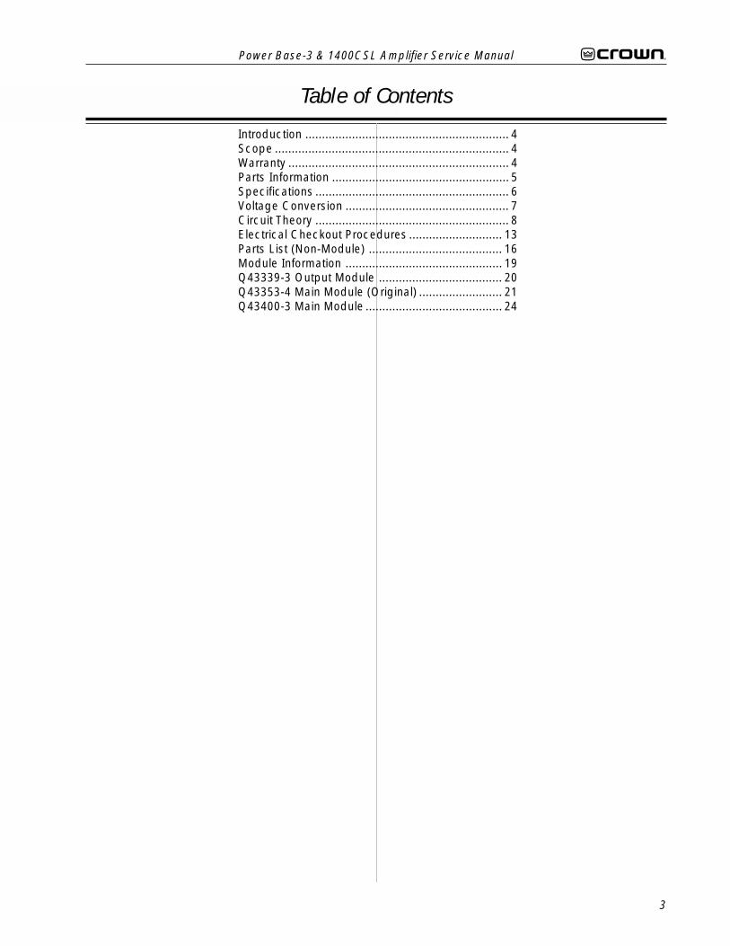
Introduction ............................................................. 4Scope ...................................................................... 4Warranty .................................................................. 4Parts Information ..................................................... 5Specifications .......................................................... 6Voltage Conversion ................................................. 7Circuit Theory .......................................................... 8Electrical Checkout Procedures ............................ 13Parts List (Non-Module) ........................................ 16Module Information ............................................... 19Q43339-3 Output Module ..................................... 20Q43353-4 Main Module (Original) ......................... 21Q43400-3 Main Module ......................................... 24
Table of Contents
Power Base-3 & 1400CSL Amplifier Service Manual
4
CrownTechnical Support Group
Factory ServiceParts Department
Mailing Address:PO Box 1000
Elkhart, IN USA 46515-1000
Shipping Address:57620 C.R. 105
Elkhart, IN USA 46517
Phone: (219) 294-8200Toll Free: (800) 342-6939
FAX: (219) 294-8301
This manual contains service information on Crownpower amplifiers. It is designed to be used in conjunc-tion with the applicable Owner's Manual. However,some important information is duplicated in this Ser-vice Manual in case the Owner's Manual is not readilyavailable.
NOTE: THE INFORMATION IN THIS MANUAL IS INTENDEDFOR USE BY AN EXPERIENCED TECHNICIAN ONLY!
SCOPEThis Service Manual includes several sections. Thesesections include Parts Ordering, Specifications, Volt-age Conversion, Circuit Theory, Factory Test Proce-dures, Mechanical Parts Lists, and Module Parts Lists.Schematics are attached. Note that component partswith circuit board comprise a complete module. Mod-ule part numbers are always associated with a spe-cific circuit board, although an unpopulated circuitboard may be built up with different parts to createdifferent modules. Note that Crown does not sell blank(unpopulated) circuit boards.
Each of the compact audio power amplifiers aredesigned for professional or commercial use. Provid-ing high power amplification from 20Hz to 20KHz withminimum distortion, they feature balanced inputs withbridged and parallel monophonic capability. Specificfeatures vary depending on model family.
WARRANTYEach Owner's Manual contains basic policies as re-lated to the customer. In addition it should be statedthat this service documentation is meant to be usedonly by properly trained service personnel. Becausemost Crown products carry a 3 Year Full Warranty(including round trip shipping within the United States),all warranty service should be referred to the CrownFactory or Authorized Warranty Service Center. Seethe applicable Owner’s Manual for warranty details. Tofind the location of the nearest Authorized ServiceCenter or obtain instructions for receiving Crown Fac-tory Service please contact the Crown Technical Sup-port Group (within North America) or your Crown/Amcron Importer (outside North America).
Introduction
Power Base-3 & 1400CSL Amplifier Service Manual
5
Parts Information
shipment on a C.O.D. or pre-payment (check or creditcard) basis.
TERMSNormal terms are pre-paid. Net-30 Days applies toonly those firms having pre-established accounts withCrown. If pre-paying, the order must be packed andweighed before a total bill can be established, afterwhich an amount due will be issued and shipmentmade upon receipt of pre-payment. New parts re-turned for credit are subject to a 10% re-stocking fee,and authorization from the Crown Parts Departmentmust be obtained before returning parts for credit.
Crown is not a general parts warehouse. Parts sold bythe Crown Parts Department are solely for servicingCrown/Amcron products. Part prices and availabil-ity are subject to change without notice.
GENERAL INFORMATIONLater sections include both mechanical and electricalparts lists for this product. The parts listed are currentas of the date printed. Crown reserves the right tomodify and improve its products for the benefit of itscustomers.
PART NUMBERING SYSTEMSAs of the printing of this manual, Crown is using twonumbering systems. The elder system always useseight characters. The first character is a letter. Com-mon letters used are C, D, H, M, P, and Q. The secondthrough sixth characters are numbers. The numbersbuild sequentially (for each prefix letter) as new partsare added to our parts inventory system. (In somecases there will be a space then a four characternumber after the prefix letter; the space is considereda character.) The seventh character is usually a hy-phen, though it may be a letter to indicate a revision orspecial note. The last character is called a check-digit,and is useful to Crown for internal tracking.
Crown is in the process of converting to a new partnumber system. Length may vary from eight to twelvecharacters. There is still a letter prefix, then fivenumbers. These five numbers identify a type of part.The seventh character is a hyphen. Remaining char-acters identify the details of the type of part identifiedby the first part of the number.
STANDARD AND SPECIAL PARTSMany smaller electrical and electronic parts used byCrown are stocked by and available from electronicsupply houses. However, some electronic parts thatappear to be standard are actually special. A partordered from Crown will assure an acceptable re-placement. Structural items such as modules andpanels are available from Crown only.
ORDERING PARTSWhen ordering parts, be sure to give the productmodel, and include a description and part number(CPN/DPN) from the parts listing. Price quotes areavailable on request.
SHIPMENTShipment will be normally made by UPS or best othermethod unless you specify otherwise. Shipments aremade to and from Elkhart, Indiana USA, only. Estab-lished accounts with Crown will receive shipmentfreight prepaid and will be billed. All others will receive
CrownParts Department
Mailing Address:PO Box 1000
Elkhart, IN USA 46515-1000
Shipping Address:57620 C.R. 105
Elkhart, IN USA 46517
Phone: (219) 294-8210or: (219) 294-8211
Toll Free: (800) 342-6939FAX: (219) 294-8301
Power Base-3 & 1400CSL Amplifier Service Manual
6
Specifications
Unless noted otherwise, all specifications are basedon driving an 8 ohm load per channel, both channelsdriven, the sensitivity switch in the 26dB position, theAC supply is 120VAC at 60Hz. Crown specificationsare guaranteed through the warranty period (normally3 years). Because our testing methods are more strin-gent than our published specifications, every Crownamplifier will exceed its published specifications.
POWERPower8 Ohm Stereo—500W/Ch4 Ohm Stereo—700W/Ch8 Ohm Bridge Mono—1500W4 Ohm Parallel Mono—1050W2 Ohm Parallel Mono—1515W
Load Impedances: Rated for 16, 8, 4, and 2 (parallelmono only) Ohm operation; safe with all types of loads,even totally reactive loads.
AC Mains: 120VAC at 60 Hz with standard 3 wiregrounded 15A connector with single voltage trans-former and fan for North American units; 100VAC,120VAC, 220VAC, and 240VAC at 50 or 60 Hz whenequipped with universal transformer, applicable fan,and other applicable hardware with country specificpower cord. Note that at 50 Hz fan speed is reduced.
PERFORMANCEFrequency Response: ±0.1dB from 20 Hz to 20 kHz at 1Watt.
Phase Response: ±10° from 10 Hz to 20 kHz at 1 Watt.
Signal to Noise Ratio: A-weighted, better than 105 dBbelow full rated output. Better than 100 dB below fullrated output from 20 Hz to 20 kHz.
Total Harmonic Distortion (THD): <0.05% from 20 Hz to1 kHz, increasing linearly to 0.1% at 20 kHz at 500W.
I.M. Distortion: <0.05% from 170 milliwatts to 500 W at26 dB gain.
Slew Rate: >13V per microsecond.
Damping Factor: >1000 from 10 Hz to 400 Hz.
DC Offset: <10 millivolts.
Input Impedance: Nominally 20K ohms balanced; 10Kohms unbalanced.
Output Impedance: <10 milliohms in series with <2microhenries.
Protection Systems: Output Device Emulation Protec-tion (ODEP) limits drive in the event of dangerousdynamic thermal conditions without interrupting power.Current limiting for shorted load protection. DC/LF andcommon mode output current Fault circuitry to muteaudio. Delay of 4 seconds from turn on mutes amplifierto prevent dangerous turn-on transients. High voltagecircuit breaker in main transformer primary and lowvoltage fuse in fan primary. Slew rate limiting toprevent RF burn out.
MECHANICALInput Connectors: Balanced 1/4 inch phone jacks. Op-tional XLR inputs with MT-XLR accessory.
Output Connectors: Color-coded 5-way binding postson 3/4 inch centers; spaced 3/4 inch apart.
Front Panel Controls: A rocker on/off power switch.
Back Panel Controls: A three-position switch whichselects Stereo, Bridge-Mono, or Parallel-Mono mode;a two position input ground-lift switch, and level con-trols for each channel.
Internal Controls: A three-position switch selects 0.775V,1.4V, or 26 dB voltage gain input sensitivity.
Indicators: Red Enable indicator shows on/off status oflow-voltage power supply.
Construction: Black splatter-coat steel chassis withspecially designed flow-through ventilation system.
Mounting: Standard EIA 310 front-panel rack mountwith supports for supplemental rear corner mounting.
Dimensions: 19 inches wide, 3.5 inches high, 16 inchesdeep behind front mounting surface.
Weight: 36 lbs. Shipping; 40 lbs.
Power Base-3 & 1400CSL Amplifier Service Manual
7
Voltage Conversion
Note: The only versions of thisproduct produced at the CrownFactory with international volt-age capabilities are the CSLversions built specifically forsale outside the United States.
P16P10
P15
P14
P13
P12
P11
P9
P8
P7
P6
P5
P4
P3
P2
P1
P22
P21
P18 P17
P19
P20
F1F100
BRN
BLU
100V Connections:P10 to P15P11 to P14P7 to P12
120V Connections:P10 to P16P11 to P14P7 to P13
220V Connections:P10 to P15P9 to P14P8 to P13
240V Connections:P10 to P16P9 to P14P8 to P13
For list of applicabletransformer, fuse F100,fanformer, and powercord refer to voltage-parts cross-reference.
S1 Power Switch
PB/CSL Universal Fuse Board
Specific parts are required for the PB-3/1400CSL inorder to be used at different international line volt-ages. Refer also to Mechanical Parts Lists.
Voltage Specific Parts:30A Breaker for 100-120V Operation C 9837-315A Breaker for 220-240V Operation C 9839-90.5A F1, Low Voltage* A10285-7Power Transformer (United States) D 8598-1Power Transformer (Universal) D 8601-3Transmotor 120V 60 Hz Only H43065-4Transmotor 120V 50-60 Hz H43055-5
*Use 0.3A for UL® approval A10285-33
Power Base-3 & 1400CSL Amplifier Service Manual
8
Theory
OVERVIEWIt should be noted from the outset that the PB-3 and1400CSL amplifiers are electrically and mechanicallyidentical products. The only differences, from a ser-vice perspective, are cosmetic. It should also benoted that over time Crown makes improvements andchanges for various reasons. This manual is up to dateas of the time of writing. For additional informationregarding these amplifiers, refer to the applicableTechnical Notes provided by Crown for this product.
This section of the manual explains the general opera-tion of a typical Crown power amplifier. Topics cov-ered include Front End, Grounded Bridge, and ODEP.Due to variations in design from vintage to vintage(and similarities with other Crown products) the theoryof operation remains simplified.
FEATURESPower Base/CSL amplifiers utilize numerous Crowninnovations including grounded bridge and ODEPtechnologies. Cooling techniques make use of thewhat is essentially air conditioner technology. Air flowsbottom to top, and front to side. Air flows a shortdistance across a wide heatsink. This type of air flowprovides significantly better cooling than the “windtunnel” technology used by many other manufactur-ers. Output transistors are of the metal can type ratherthan plastic case. This allows for a significantly higherthermal margin for the given voltage and currentratings. All devices used are tested and graded toensure maximum reliability. Another electronic tech-nique used is negative feedback. Almost all poweramplifiers utilize negative feedback to control gainand provide stability, but Crown uses multiple nestedfeedback loops for maximum stability and greatlyimproved damping. Most Crown amplifiers have damp-ing in excess of 1000 in the bass frequency range. Thisfeedback, along with our compensation and ultra-lowdistortion output topology, make Crown amplifierssuperior.
Features specific to the Power Base/CSL Series’ in-clude a single core transformer (one primary with twoindependent ungrounded secondaries), a full time fullspeed fan which also serves as the low voltagetransformer, slew rate limiting, and audio muting fordelay or protective action. This amplifier can operatein either a Bridged or Parallel Mono mode as well asdual (stereo). A sensitivity switch allows selection ofinput voltage required for rated output. Level controlsare rear mounted. The only indicator provided tells the
operator that the low voltage supply is energized. Ingeneral, the packaging of this model is designed formaximum watt/price/weight/size value. It is the mostbasic grounded bridge amplifier series now availablefrom Crown.
For additional details refer to the specification section,or to the applicable Owner’s Manual.
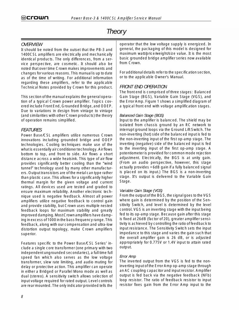
FRONT END OPERATIONThe front end is comprised of three stages: BalancedGain Stage (BGS), Variable Gain Stage (VGS), andthe Error Amp. Figure 1 shows a simplified diagram ofa typical front end with voltage amplification stages.
Balanced Gain Stage (BGS)Input to the amplifier is balanced. The shield may beisolated from chassis ground by an RC network tointerrupt ground loops via the Ground Lift Switch. Thenon-inverting (hot) side of the balanced input is fed tothe non-inverting input of the first op-amp stage. Theinverting (negative) side of the balanced input is fedto the inverting input of the first op-amp stage. Apotentiometer is provided for common mode rejectionadjustment. Electrically, the BGS is at unity gain.(From an audio perspective, however, this stageactually provides +6dB gain if a fully balanced signalis placed on its input.) The BGS is a non-invertingstage. It’s output is delivered to the Variable GainStage.
Variable Gain Stage (VGS)From the output of the BGS, the signal goes to the VGSwhere gain is determined by the position of the Sen-sitivity Switch, and level is determined by the levelcontrol. VGS is an inverting stage with the input beingfed to its op-amp stage. Because gain after this stageis fixed at 26dB (factor of 20), greater amplifier sensi-tivity is achieved by controlling the ratio of feedback toinput resistance. The Sensitivity Switch sets the inputimpedance to this stage and varies the gain such thatthe overall amplifier gain is 26 dB, or is adjustedappropriately for 0.775V or 1.4V input to attain ratedoutput.
Error AmpThe inverted output from the VGS is fed to the non-inverting input of the Error Amp op-amp stage throughan AC coupling capacitor and input resistor. Amplifieroutput is fed back via the negative feedback (NFb)loop resistor. The ratio of feedback resistor to inputresistor fixes gain from the Error Amp input to the
Power Base-3 & 1400CSL Amplifier Service Manual
9
Theory
output of the amplifier at 26 dB. Diodes preventoverdriving the Error Amp. Because the Error Ampamplifies the difference between input and outputsignals, any difference in the two waveforms willproduce a near open loop gain condition which in turnresults in high peak output voltage. The output of theError Amp, called the Error Signal (ES) drives theVoltage Translators.
VOLTAGE AMPLIFICATIONThe Voltage Translator stage separates the output ofthe Error Amp into balanced positive and negativedrive voltages for the Last Voltage Amplifiers (LVAs),translating the signal from ground referenced ±15V to±Vcc reference. LVAs provide the main voltage ampli-fication and drive the High Side output stages. Gainfrom Voltage Translator input to amplifier output is afactor of 25.2.
Voltage TranslatorsA voltage divider network splits the Error Signal (ES)into positive and negative drive signals for the bal-anced voltage translator stage. These offset referencevoltages drive the input to the Voltage Translatortransistors. A nested NFb loop from the output of theamplifier mixes with the inverted signal riding on theoffset references. This negative feedback fixes gain atthe offset reference points (and the output of the ErrorAmp) at a factor of -25.2 with respect to the amplifieroutput. The Voltage Translators are arranged in acommon base configuration for non-inverting voltagegain with equal gain. They shift the audio from the±15V reference to VCC reference. Their outputs drivetheir respective LVA.
Also tied into the Voltage Translator inputs are ODEPlimiting transistors and control/protection transistors.The ODEP transistors steal drive as dictated by theODEP circuitry (discussed later). The control/protec-tion transistors act as switches to totally shunt audio toground during the turn-on delay, or during a DC/LF orFault protective action.
Last Voltage Amplifiers (LVAs)The Voltage Translator stage channels the signal tothe Last Voltage Amplifiers (LVA's) in a balancedconfiguration. The +LVA and -LVA, with their push-pulleffect through the Bias Servo, drive the fully comple-mentary output stage. The LVAs are configured ascommon emitter amplifiers. This configuration pro-vides sufficient voltage gain and inverts the audio. Thepolarity inversion is necessary to avoid an overallpolarity inversion from input jack to output jack, and itallows the NFb loop to control Error Amp gain byfeeding back to its non-inverting input (with its polarityopposite to the output of the VGS). With the addedvoltage swing provided by the LVAs, the signal thengains current amplification through the Darlingtonemitter-follower output stage.
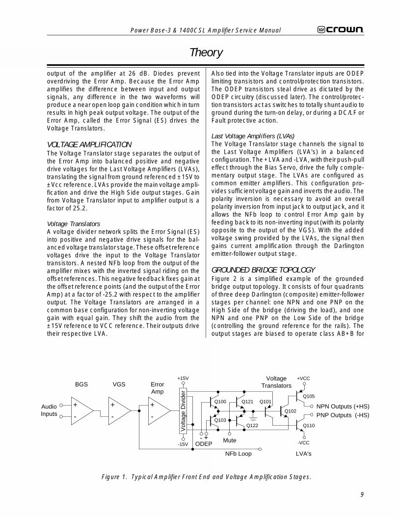
GROUNDED BRIDGE TOPOLOGYFigure 2 is a simplified example of the groundedbridge output topology. It consists of four quadrantsof three deep Darlington (composite) emitter-followerstages per channel: one NPN and one PNP on theHigh Side of the bridge (driving the load), and oneNPN and one PNP on the Low Side of the bridge(controlling the ground reference for the rails). Theoutput stages are biased to operate class AB+B for
+
-
+
-
+
-
BGS VGS ErrorAmp
AudioInputs
Vol
tage
Div
ider
NFb Loop
+-ODEP
Mute
+15V
-15V
+VCC
-VCC
NPN Outputs (+HS)
PNP Outputs (-HS)
Q100
Q103
Q121
Q122
Q101
Q102
Q105
Q110
VoltageTranslators
LVA's
Figure 1. Typical Amplifier Front End and Voltage Amplification Stages.
Power Base-3 & 1400CSL Amplifier Service Manual
10
ultra low distortion in the signal zero-crossing regionand high efficiency.
High Side (HS)The High Side (HS) of the bridge operates much likea conventional bipolar push-pull output configuration.As the input drive voltage becomes more positive, theHS NPN conducts and delivers positive voltage to theload. Eventually the NPN devices reach full conduc-tion and +Vcc is across the load. At this time the HSPNP is biased off. When the drive signal is negativegoing, the HS PNP conducts to deliver -Vcc to the loadand the HS NPN stage is off.
The output of the +LVA drives the base of predriverdevice. Together, the predriver and driver form thefirst two parts of the three-deep Darlington and arebiased class AB. They provide output drive throughthe bias resistor, bypassing the output devices, atlevels below about 100mW. An RLC network betweenthe predriver and driver provide phase shift compen-sation and limit driver base current to safe levels.Output devices are biased class B, just below cutoff.At about 100mW output they switch on to conduct highcurrent to the load. Together with predriver and driver,the output device provide an overall class AB+Boutput.
The negative half of the HS is almost identical to thepositive half, except that the devices are PNP. One
Theory
+
-
+Vcc (Positive Rail)
-Vcc (Negative Rail)
Load(speaker)
Inputsignal
HIGH SIDE LOW SIDE
Inverting Op-amp
Figure 2. Crown Patented Grounded Bridge Topology
difference is that the PNP bias resistor is slightlygreater in value so that PNP output devices run closerto the cutoff level under static (no signal) conditions.This is because PNP devices require greater drivecurrent.
HS bias is regulated by Q18, the Bias Servo. Q18 is aVbe multiplier which maintains approximately 3.3VVce under static conditions. The positive and negativehalves of the HS output are in parallel with this 3.3V.With a full base-emitter on voltage drop acrosspredrivers and drivers, the balance of voltage resultsin approximately .35V drop across the bias resistors inthe positive half, and about .5V across the bias resistorin the negative half. Q18 conduction (and thus bias) isadjustable.
A diode string prevents excessive charge build upwithin the high conduction output devices when off.Flyback diodes shunt back-EMF pulses from reactiveloads to the power supply to protect output devicesfrom dangerous reverse voltage levels. An outputterminating circuit blocks RF on output lines fromentering the amplifier through its output connectors.
Low Side (LS)The Low Side (LS) operates quite differently. Thepower supply bridge rectifier is not ground refer-enced, nor is the secondary of the main transformer.
Power Base-3 & 1400CSL Amplifier Service Manual
11
In other words, the high voltage power supply floatswith respect to ground, but ±Vcc remain constant withrespect to each other. This allows the power supply todeliver +Vcc and -Vcc from the same bridge rectifierand filter as a total difference in potential, regardlessof their voltages with respect to ground. The LS usesinverted feedback from the HS output to control theground reference for the rails (±Vcc). Both LS quad-rants are arranged in a three-deep Darlington and arebiased AB+B in the same manner as the HS.
When the amplifier output swings positive, the audio isfed to an op-amp stage where it is inverted. Thisinverted signal is delivered directly to the bases of thepositive (NPN) and negative (PNP) LS predrivers. Thenegative drive forces the LS PNP devices on (NPNoff). As the PNP devices conduct, Vce of the PNPDarlington drops. With LS device emitters tied toground, -Vcc is pulled toward ground reference.Since the power supply is not ground referenced (andthe total voltage from +Vcc to -Vcc is constant) +Vccis forced higher above ground potential. This contin-ues until, at the positive amplifier output peak, -Vcc =0V and +Vcc equals the total power supply potentialwith a positive polarity. If, for example, the powersupply produced a total of 70V from rail to rail (±35VDCmeasured from ground with no signal), the amplifieroutput would reach a positive peak of +70V.
Conversely, during a negative swing of the HS outputwhere HS PNP devices conduct, the op-amp wouldoutput a positive voltage forcing LS NPN devices toconduct. This would result in +Vcc swinging towardground potential and -Vcc further from ground poten-tial. At the negative amplifier output peak, +Vcc = 0Vand -Vcc equals the total power supply potential witha negative polarity. Using the same example as above,a 70V supply would allow a negative output peak of -70V. In summary, a power supply which produces atotal of 70VDC rail to rail (or ±35VDC statically) iscapable of producing 140V peak-to-peak at the ampli-fier output when the grounded bridge topology isused. The voltage used in this example are relativelyclose to the voltages of the PB-1/460CSL.
The total effect is to deliver a peak to peak voltage tothe speaker load which is twice the voltage producedby the power supply. Benefits include full utilization ofthe power supply (it conducts current during bothhalves of the output signal; conventional designsrequire two power supplies per channel, one positiveand one negative), and never exposing any output
Theory
device to more than half of the peak to peak outputvoltage (which does occur in conventional designs).
Low side bias is established by a diode string whichalso shunts built up charges on the output devices.Bias is adjustable via potentiometer. Flyback diodesperform the same function as the HS flybacks. Theoutput of the LS is tied directly to chassis ground viaground strap.
OUTPUT DEVICE EMULATION PROTECTION(ODEP)To further protect the output stages, a specially devel-oped ODEP circuit is used. It produces a complexanalog output signal. This signal is proportional to thealways changing safe-operating-area margin of theoutput transistors. The ODEP signal controls the Volt-age Translator stage by removing drive that mayexceed the safe-operating-area of the output stage.
ODEP senses output current by measuring the volt-age dropped across LS emitter resistors. LS NPNcurrent (negative amplifier output) and +Vcc aresensed, then multiplied to obtain a signal proportionalto output power. Positive and negative ODEP voltagesare adjustable via two potentiometers. Across ±ODEPare a PTC and a thermal sense (current source). ThePTC is essentially a cutoff switch that causes hardODEP limiting if heatsink temperature exceeds a safemaximum, regardless of signal level. The thermalsense causes the differential between +ODEP and –ODEP to decrease as heatsink temperature increases.An increase in positive output signal output into a loadwill result in –ODEP voltage dropping; an increase innegative output voltage and current will cause +ODEPvoltage to drop. A complex RC network between the±ODEP circuitry is used to simulate the thermal barri-ers between the interior of the output device die(immeasurable by normal means) and the time delayfrom heat generation at the die until heat dissipates tothe thermal sensor. The combined effects of thermalhistory and instantaneous dynamic power level resultin an accurate simulation of the actual thermal condi-tion of the output transistors.
Power Base-3 & 1400CSL Amplifier Service Manual
12
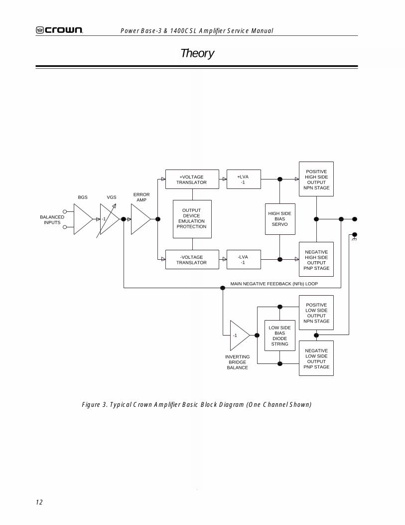
Theory
NEGATIVELOW SIDEOUTPUT
PNP STAGE
POSITIVELOW SIDEOUTPUT
NPN STAGE
NEGATIVEHIGH SIDEOUTPUT
PNP STAGE
POSITIVEHIGH SIDEOUTPUT
NPN STAGE
HIGH SIDEBIAS
SERVO
+LVA-1
-LVA-1
+VOLTAGETRANSLATOR
-VOLTAGETRANSLATOR
OUTPUTDEVICE
EMULATIONPROTECTION
ERRORAMP
VGSBGS
BALANCEDINPUTS
INVERTINGBRIDGE
BALANCE
LOW SIDEBIAS
DIODESTRING
-1
-1
MAIN NEGATIVE FEEDBACK (NFb) LOOP
Figure 3. Typical Crown Amplifier Basic Block Diagram (One Channel Shown)
Power Base-3 & 1400CSL Amplifier Service Manual
13
Electrical Checkout Procedures
GENERAL INFORMATIONThe following test procedures are to be used to verifyoperation of this amplifier. DO NOT connect a load orinject a signal unless directed to do so by the proce-dure. These tests, though meant for verification andalignment of the amplifier, may also be very helpful introubleshooting. For best results, tests should beperformed in order.
All tests assume that AC power is from a regulated 120VAC source. Test equipment includes an oscillo-scope, a DMM, a signal generator, loads, and I.M.D.and T.H.D. noise test equipment.
STANDARD INITIAL CONDITIONSLevel controls fully clockwise.Stereo/Mono switch in Stereo.Sensitivity switch in 26 dB fixed gain position.It is assumed, in each step, that conditions of theamplifier are per these initial conditions unless other-wise specified.
TEST 1: DC OFFSETSpec: 0 VDC, ±10 mV.Initial Conditions: Controls per standard, inputs shorted.Procedure: Measure DC voltage at the output connec-tors (rear panel). There is no adjustment for outputoffset. If spec is not met, there is an electrical malfunc-tion. Slightly out of spec measurement is usually dueto U104/U204 out of tolorance.
TEST 2: OUTPUT BIAS ADJUSTMENTSpec: 300 to 320 mVDC.Initial Conditions: Controls per standard, heatsink tem-perature less than 40°C.Procedure: Measure DC voltages on the output moduleacross R02, adjust R26 if necessary. Measure DCvoltages on the output module across R21, adjust R23if necessary. Repeat for second channel.
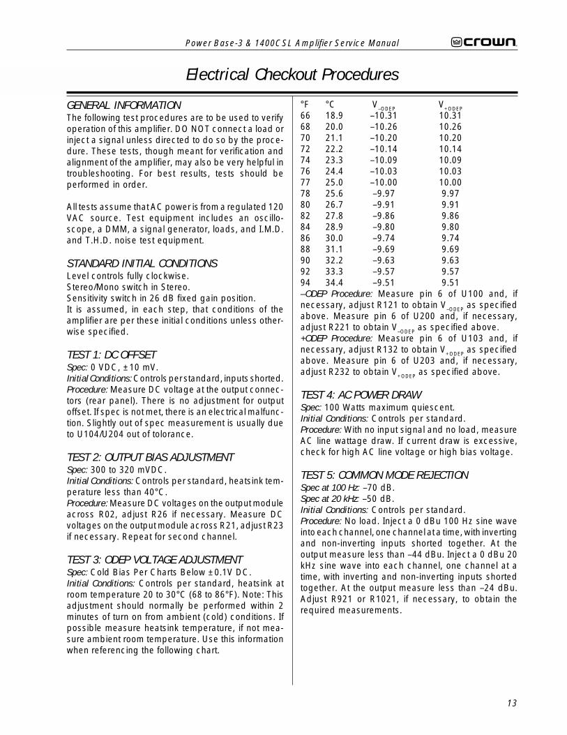
TEST 3: ODEP VOLTAGE ADJUSTMENTSpec: Cold Bias Per Charts Below ±0.1V DC.Initial Conditions: Controls per standard, heatsink atroom temperature 20 to 30°C (68 to 86°F). Note: Thisadjustment should normally be performed within 2minutes of turn on from ambient (cold) conditions. Ifpossible measure heatsink temperature, if not mea-sure ambient room temperature. Use this informationwhen referencing the following chart.
°F °C V–ODEP V+ODEP
66 18.9 –10.31 10.3168 20.0 –10.26 10.2670 21.1 –10.20 10.2072 22.2 –10.14 10.1474 23.3 –10.09 10.0976 24.4 –10.03 10.0377 25.0 –10.00 10.0078 25.6 –9.97 9.9780 26.7 –9.91 9.9182 27.8 –9.86 9.8684 28.9 –9.80 9.8086 30.0 –9.74 9.7488 31.1 –9.69 9.6990 32.2 –9.63 9.6392 33.3 –9.57 9.5794 34.4 –9.51 9.51–ODEP Procedure: Measure pin 6 of U100 and, ifnecessary, adjust R121 to obtain V–ODEP as specifiedabove. Measure pin 6 of U200 and, if necessary,adjust R221 to obtain V–ODEP as specified above.+ODEP Procedure: Measure pin 6 of U103 and, ifnecessary, adjust R132 to obtain V+ODEP as specifiedabove. Measure pin 6 of U203 and, if necessary,adjust R232 to obtain V+ODEP as specified above.
TEST 4: AC POWER DRAWSpec: 100 Watts maximum quiescent.Initial Conditions: Controls per standard.Procedure: With no input signal and no load, measureAC line wattage draw. If current draw is excessive,check for high AC line voltage or high bias voltage.
TEST 5: COMMON MODE REJECTIONSpec at 100 Hz: –70 dB.Spec at 20 kHz: –50 dB.Initial Conditions: Controls per standard.Procedure: No load. Inject a 0 dBu 100 Hz sine waveinto each channel, one channel at a time, with invertingand non-inverting inputs shorted together. At theoutput measure less than –44 dBu. Inject a 0 dBu 20kHz sine wave into each channel, one channel at atime, with inverting and non-inverting inputs shortedtogether. At the output measure less than –24 dBu.Adjust R921 or R1021, if necessary, to obtain therequired measurements.
Power Base-3 & 1400CSL Amplifier Service Manual
14
TEST 6: VOLTAGE GAINSpec 26dB Gain: ±3%.Spec 0.775V Sensitivity: ±6%.Spec 1.4V Sensitivity: +12%/–6%.Initial Conditions: Controls per standard.Procedure: No load connected. Inject a 0.775 VAC 1kHz sine wave with the Sensitivity Switch in the 26 dBposition. Measure 15.5 VAC ±0.5 VAC at the amplifieroutput. Inject a 0.775 VAC 1 kHz sine wave with theSensitivity Switch in the 0.775V position. Measure 65.7VAC ±3.9 VAC at the amplifier output. Inject a 1.4 VAC1 kHz sine wave with the Sensitivity Switch in the 1.4Vposition. Measure 65.7 VAC +7.8/-3.9 VAC at theamplifier output. Return the Sensitivity Switch to the 26dB position.
TEST 7: PHASE RESPONSESpec: ±10° from 10 Hz to 20 kHz at 1 Watt.Initial Conditions: Controls per standard, 8 ohm load oneach channel.Procedure: Inject a 1 kHz sine wave and adjust for 1Watt output (2.8 VAC). Check input and output signalsagainst each other, input and output signals must bewithin 10° of each other.
TEST 8: LEVEL CONTROLSSpec: Level controlled by level controls.Initial Conditions: Controls per standard.Procedure: No Load. Inject a 1 kHz sine wave. Withlevel controls fully clockwise you should see full gain.As controls are rotated counterclockwise, observesimilar gain reduction in each channel. When com-plete, return level controls to fully clockwise position.
TEST 9: CURRENT LIMITSpec: Current Limit at 38 ±3 AmpsInitial Conditions: Controls per standard.Procedure: Load each channel to 1 Ohm. Inject a 1 kHzdifferentiated (or 10% duty cycle) square wave andincrease output level until current limit occurs. Currentlimit should occur at 38 ±3 Amps (38 Vpk) with outputdevice Vce less than 40 Vpk. Observe clean (nooscillations) current clipping.
Electrical Checkout Procedures
TEST 10: SLEW RATE & 10 KHZ SQUARE WAVESpec: >17V/µS.Initial Conditions: Controls per standard.Procedure: Load each channel to 8 ohms. Inject a 10kHz square wave to obtain 65 volts peak-to-peak ateach output. Observe the slope of the square wave. Itshould typically measure 17 to 25 V/µS. Also, thesquare wave must not include overshoot, ringing, orany type of oscillation.
TEST 11: CROSSTALKSpec: -60dB at 20 kHz.Initial Conditions: Controls per standard. Terminateinput of channel not driven with 600 ohms.Procedure: 8 ohm load on each channel. Inject a 20 kHzsine wave into the Channel 1 input and increase outputlevel to 62 VAC. Measure less than 62 mVAC at theoutput of Channel 2. Inject a 20 kHz sine wave into theChannel 2 input and increase output level to 62 VAC.Measure less than 62 mVAC at the output of Channel1.
TEST 12: OUTPUT POWERSpec at 8 Ohm Stereo: 540W at 0.1% THD.Spec at 4 Ohm Stereo: 760W at 0.1% THD.International 8 Ohm Stereo:International 8 Ohm Stereo:International 8 Ohm Stereo:International 8 Ohm Stereo:International 8 Ohm Stereo: 510W at 0.1% THD.International 4 Ohm Stereo:International 4 Ohm Stereo:International 4 Ohm Stereo:International 4 Ohm Stereo:International 4 Ohm Stereo: 680W at 0.1% THD.Initial Conditions: Controls per standard.Procedure: Load each channel to 8 ohms. Inject a 1 kHzsine wave and measure at least 65.7 VAC at the outputof each channel. Load each channel to 4 ohms. Injecta 1 kHz sine wave and measure at least 55.1 VAC. Allpower measurements must be at less than 0.1% THD.
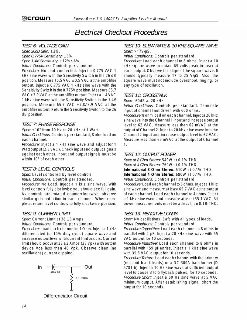
TEST 13: REACTIVE LOADSSpec: No oscillations. Safe with all types of loads.Initial Conditions: Controls per standard.Procedure Capacitive: Load each channel to 8 ohms inparallel with 2 µF. Inject a 20 kHz sine wave with 55VAC output for 10 seconds.Procedure Inductive: Load each channel to 8 ohms inparallel with 159 µHenries. Inject a 1 kHz sine wavewith 35.8 VAC output for 10 seconds.Procedure Torture: Load each channel with the primary(red and black leads) of a DC-300A transformer (D5781-6). Inject a 10 Hz sine wave at sufficient outputlevel to cause 3 to 5 flyback pulses, for 10 seconds.Procedure Short: Inject a 60 Hz sine wave at 5 VACminimum output. After establishing signal, short theoutput for 10 seconds.
In Out.047 uF
1K Ohm
Differenciator Circuit
Power Base-3 & 1400CSL Amplifier Service Manual
15
Electrical Checkout Procedures
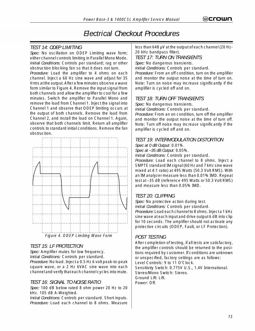
TEST 14: ODEP LIMITINGSpec: No oscillation on ODEP Limiting wave form;either channel controls limiting in Parallel Mono Mode.Initial Conditions: Controls per standard; rag or otherobstruction blocking fan so that it does not turn.Procedure: Load the amplifier to 4 ohms on eachchannel. Inject a 60 Hz sine wave and adjust for 35Vrms at the output. After a few minutes observe a waveform similar to Figure 4. Remove the input signal fromboth channels and allow the amplifier to cool for a fewminutes. Switch the amplifier to Parallel Mono andremove the load from Channel 1. Inject the signal intoChannel 1 and observe that ODEP limiting occurs atthe output of both channels. Remove the load fromChannel 2, and install the load on Channel 1. Again,observe that both channels limit. Return all amplifiercontrols to standard initial conditions. Remove the fanobstruction.
TEST 15: LF PROTECTIONSpec: Amplifier mutes for low frequency.Initial Conditions: Controls per standard.Procedure: No load. Inject a 0.5 Hz 6 volt peak-to-peaksquare wave, or a 2 Hz 6VAC sine wave into eachchannel and verify that each channel cycles into mute.
TEST 16: SIGNAL TO NOISE RATIOSpec: 100 dB below rated 8 ohm power 20 Hz to 20kHz. 105 dB A-Weighted.Initial Conditions: Controls per standard. Short inputs.Procedure: Load each channel to 8 ohms. Measure
less than 648 µV at the output of each channel (20 Hz-20 kHz bandpass filter).TEST 17: TURN ON TRANSIENTSSpec: No dangerous transients.Initial Conditions: Controls per standard.Procedure: From an off condition, turn on the amplifierand monitor the output noise at the time of turn on.Note: Turn on noise may increase significantly if theamplifier is cycled off and on.
TEST 18: TURN OFF TRANSIENTSSpec: No dangerous transients.Initial Conditions: Controls per standard.Procedure: From an on condition, turn off the amplifierand monitor the output noise at the time of turn off.Note: Turn off noise may increase significantly if theamplifier is cycled off and on.
TEST 19: INTERMODULATION DISTORTIONSpec at 0 dB Output: 0.01%.Spec at –35 dB Output: 0.05%.Initial Conditions: Controls per standard.Procedure: Load each channel to 8 ohms. Inject aSMPTE standard IM signal (60 Hz and 7 kHz sine wavemixed at 4:1 ratio) at 495 Watts (50.3 Volt RMS). Withan IM analyzer measure less than 0.01% IMD. Repeattest at –35 dB (reference 495 Watts or 50.3 Volt RMS)and measure less than 0.05% IMD.
TEST 20: CLIPPINGSpec: No protective action during test.Initial Conditions: Controls per standard.Procedure: Load each channel to 8 ohms. Inject a 1 kHzsine wave at each input and drive output 6 dB into clipfor 10 seconds. The amplifier should not activate anyprotective circuits (ODEP, Fault, or LF Protection).
POST TESTINGAfter completion of testing, if all tests are satisfactory,the amplifier controls should be returned to the posi-tions required by customer. If conditions are unknownor unspecified, factory settings are as follows:Level Controls: 9 to 11 O’Clock.Sensitivity Switch: 0.775V U.S., 1.4V International.Stereo/Mono Switch: Stereo.Ground Lift: Lift.Power: Off.
Figure 4. ODEP Limiting Wave Form
Power Base-3 & 1400CSL Amplifier Service Manual
16
Parts List (Non-Module)
SUPPLIMENTAL ITEMSCPN ITEM QTYD 4137-2 Nylon Thumbscrew Washer 4C 3342-0 Feet, Black Self-Stick 4A10087-71012 10-32 .75 Machine (Rack Screw) 4K80607-3 PB Series Owners Manual 1
POWER SUPPLYCPN ITEM QTYC 9837-3 Breaker, 30A 250VAC (100-120VAC) 1C 9839-9 Breaker, 15A 250VAC (200-240VAC) 1A10285-33 Fuse F1, .3A Slo Blow (120V 60Hz UL approved only) 1A10285-7 Fuse F1, .5A AGC 1.25x.25 1D 8598-1 PB-3 Power Transformer (120V 60Hz Only) 1D 8601-3 1400CSL Power Transformer Universal Volt 1A10089-10832 Screw, 8-32 2.0 Ph Machine 4H43344-3 Primary Voltage Jumpers (Set of Three) 1H43437-5 Power Cord Assembly, NEMA (Standard US model) 1A10793-0503C Power Cord, EUR plug (European CSL) 1A10214-7 Strain Relief, SR7N-2 Black 1H43450-8 Power Switch Wires 1C 6487-0 Switch, 2 Pole 22A Power Rocker 1H43065-4 TransMotor (60 Hz Only) 1H43055-5 TransMotor (Universal) 1C 9939-7 Fan Blade, 4 Inch CCW 1D 8439-8 Bracket, Fan 1C 7062-0 6-32 X 5/16 FLTHD Screw 1C 8752-5 35A 400V Bridge Rectifier 2D 8438-0 Bracket, Capacitor 2A10110-70812 Screw, 8-32 X .750 Pan Head 2D 8639-3 6300µF 150V Electrolytic Capacitor 2C 9870-4 10-32 X .38 PNHD with T25 4A10095-4 #10 External Star Lockwasher 4A10098-5 1/4" Belleville Spring Washer 4D 6764-1 Washer, Shoulder Cap Assembly 4H43469-8 Blue Wires, Cap Assembly 2H43470-6 Red Wires, Cap Assembly 2
FUSE BOARD ASSEMBLY (MODULE Q43349-2)CPN ITEM QTYC 5060-6 Fuse Clip, PC Mount #926 2C 7817-7 Tab, AMP .25 FASTON PC MOUNT 22P10426-8 Fuse Board 1
LED ASSEMBLYCPN ITEM QTC 4342-9 Enable LED, Amber 1P10068B4 LED Board 1
Power Base-3 & 1400CSL Amplifier Service Manual
17
Parts List (Non-Module)
OUTPUT ASSEMBLY (ONE PER CHANNEL)CPN ITEM QTY (PER CHANNEL)C 8187-4 NPN Output Device 4C 8188-2 PNP Output Device 4C 8573-5 PNP Driver Transistor, TO-3P (2SA1186) 2C 8574-3 NPN Driver Transistor, TO-3P (2SC2837) 2D 7665-9 Clip, TO-3P Mounting 2D 7666-7 Bracket, TO-3P Heatsink 2C 8813-5 Q318/Q418 Bias Servo MPSA18/MPS8097 1B 5842-8 Tubing, #23 TFE Thin Wall Red (For C 8813-5) Request in InchesC 5826-0 S100/S200 Thermal Sense LM334Z 1B 5464-1 Tubing, #24 Teflon Thin Wall (For C 5826-0) Request in InchesD 8774-8 PTC Thermal Sensor 95DEGC 1A10315-1 Screw, 6-32-.56 Hex Washer Head 12C 9491-9 Screw, 6-32-.312 Taptite Pan Ph 23D 7796-2 Silpad Insulator (Between Chassis and Heatsinks) 1D 7797-0 Output Thru-Hole Pad Insulator 1D 8197-2 Paper Shroud 1C 9387-9 Rivet, Plastic 2F12019-0 Diode Heatsink Slug (Under diodes on Module) 1M21324-5 Heatsink, Aluminum 2H43058-9 Output Wires, Both Red and Black 1
Output Module (See Module List) 1
BACK PANEL ASSEMBLYCPN ITEM QTYA10214-7 Strain Relief (Power Cord) 1C 2823-0 Dual Binding Post Assembly 2H43437-5 Power Cord Assembly, NEMA (Standard US Model) 1A10793-0503C Power Cord EUR Plug (European CSL) 1F12605-6 Back Panel 1M46285-9 Back Panel Assembly (w/ Binding Posts & Strain Relief) 1A10019-8 Nut, #8 32-2 Captive 2
CHASSIS FRONT ASSEMBLYCPN ITEM QTYA10090-70806 Screw, 8-32-.375 Mach Ph Oval (Grille) 3A10090-70808 Screw, 8-32-.5 Mach Ph Oval (End Caps) 4A10101-5 Washer, Nylon (Grille) 3A10173-1 Clip, Grille Filter 3D 6944-9 Air Filter 1D 8465J2 End Cap 2F12435J7 Grille 1C 6487-0 Switch, 2 Pole 22A Power Rocker 1F12566J9 Overlay, PB3 1D 8638-5 Overlay, 1400CSL 1
Power Base-3 & 1400CSL Amplifier Service Manual
18
Parts List (Non-Module)
MAIN CHASSIS ASSEMBLYCPN ITEM QTYA10086-70806 Screw, 8-32 x .37 RDHD Ph 2A10086-10604 Screw, 6-32 x .25 RDHD Ph 2A10094-3 Washer, #6 Black Star 3A10094-4 Washer, #6 Zinc Star 2A10094-6 Washer, #8 Black Star 4A10099-5 Washer, #8 Nylon Shoulder 4A10109-10822 Screw, 8-18-1.375 Pan Ph 2A10110-70812 Screw, 8-32-.75 Taptite Pan Ph 2A10192-1 Snap Bushing .5 4C 6487-0 Power Switch 22A Rocker 2 Pole 1C 6912-7 Tension Retainer Board Support 2C 6913-5 Spacer Nut, 1 inch 2C 6914-3 Spacer Nut, .75 inch 2C 8812-7 5.5" Cable Tie 5C 8852-3 .5 Locking PCB Support 5C 9491-9 Screw, 6-32 x .312 Pan Head 6D 7600-6 Ground Strap (DBP to Chassis) 1D 7784-8 Label, Sensitivity Switch 1D 8606-2 Label, F1 Fuse Replacement 1F10787J3 Back Panel Plate 1D 8501-5 Cover, Top 1D 8548-6 Cover, Bottom 1A10110-70605 Screw, 6-32-.312 Taptite Ph (Covers) 20F12610-6 Chassis 1
Main Module (See Module List) 1
Power Base-3 & 1400CSL Amplifier Service Manual
19
Module Information
MODULE HISTORYThe PB-3 and 1400CSL amplifiers were introduced inJanuary of 1995. Since then there have been severalupdates and revisions, some of which called for newmodules. The following is a list of Main and Outputmodules used up to this date, June 1995. It should benoted that both the PB-3 and the 1400CSL use thesame modules.
OUTPUT MODULES: (left and right are identical)Q43339-3Original Output Module, still in production. UsesP10429-2 board.
MAIN MODULES:Q43353-4Original Main Module on D 8679-9 board. Used until6-14-95.Q43400-3Main Module on D 8827-4 board.
FUSE MODULE:Q43349-2See parts list on page 16
Power Base-3 & 1400CSL Amplifier Service Manual
20
Q43339-3 Output Module Parts List (P10429-2 Board)
Q43339-3 Output Module for PB-3:
CAPACITORSC01 C 8511-5 .047µFC02 C 8426-6 .1µFC03 C 8426-6 .1µFC04 C 6806-1 .01µFC05 C 6806-1 .01µFC06 C 6806-1 .01µFC07 C 6807-9 .001µFC08 C 6810-3 180pFC09 C 6809-5 220pFC43 C 7697-3 .01µF 500V
DIODESD01 C 2851-1 1N4004D02 C 2851-1 1N4004D03 C 2851-1 1N4004D04 C 2851-1 1N4004D05 C 2941-0 1N5402D06 C 2941-0 1N5402D07 C 2941-0 1N5402D08 C 2941-0 1N5402D09 C 2851-1 1N4004D10 C 2851-1 1N4004D11 C 2851-1 1N4004D12 C 2851-1 1N4004D13 C 2851-1 1N4004D14 C 2851-1 1N4004
INDUCTORSL00 C 6592-6 Output CoilL01 C 3510-2 470µHL02 C 3510-2 470µH
TRANSISTORSQ17 C 8508-1 NPN 2SC3298BQ19 C 8509-9 PNP 2SA1306B
Note: Q18, S100/200, Driver and Output Transistorsare not included with the module. See the OutputAssembly Parts List on page 17.
RESISTORSR00 A10266-7501 75R01 A10266-1011 100R02 C 7778-1 5.6 flame proofR03 C 6486-2 .2 5WR04 C 6486-2 .2 5WR06 C 6486-2 .2 5WR07 C 6486-2 .2 5WR09 C 7779-9 22 flame proofR10 A10266-1011 100R11 C 7317-8 2.7 5WR12 A10266-2R74 2.7 2WR13 A10266-7501 75R14 A10266-2R74 2.7 2WR16 C 6486-2 .2 5WR17 C 6486-2 .2 5WR19 C 6486-2 .2 5WR20 C 6486-2 .2 5WR21 C 7778-1 5.6 flame proofR22 C 7779-9 22 flame proofR23 C 6844-2 250 Pot LS BiasR24 A10266-1331 13KR25 A10266-2221 2.2KR26 C 6844-2 250 Pot HS BiasR27 A10266-3911 390R28 A10266-1331 13KR29 A10266-5101 51R30 A10265-10201 102R41 A10266-2201 22R42 A10266-2201 22
MISC.Board P10429-2Jumpers C 5868-2 0 Ohm Jumper (11)Clips D 6414-3 Q17/19 Hold DownJ500 J600 C 9828-2 12 Pin Header
Power Base-3 & 1400CSL Amplifier Service Manual
21
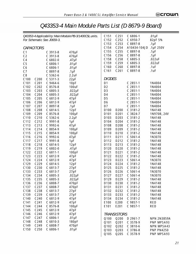
Q43353-4 Applicability: Main Module PB-3/1400CSL units.For Schematic See J0659-3.
CAPACITORSC1 C 3913-8 470µFC2 C 3913-8 470µFC4 C 6802-0 .47µFC5 C 6806-1 .01µFC6 C 6806-1 .01µFC7 C 8897-8 .1µFC8 C 5362-6 2.2uFC100 C200 C 5311-3 22µFC101 C201 C 9464-6 10pFC102 C202 C 8576-8 100uFC103 C203 C 6805-3 .022µFC104 C204 C 6805-3 .022µFC105 C205 C 6812-9 47pFC106 C206 C 6812-9 47pFC107 C207 C 8897-8 .1µFC108 C208 C 6814-5 12pFC109 C209 C 8576-8 100µFC110 C210 C 5362-6 2.2µFC112 C212 C 9991-8 1µFC113 C213 C 9992-6 47µFC114 C214 C 8854-9 100µFC115 C215 C 8854-9 100µFC116 C216 C 9992-6 47µFC117 C217 C 9991-8 1µFC118 C218 C 6814-5 12pFC119 C219 C 6802-0 .47µFC122 C222 C 6811-1 100pFC123 C223 C 6812-9 47pFC124 C224 C 6812-9 47pFC129 C229 C 6814-5 12pFC130 C230 C 6813-7 27pFC133 C233 C 6813-7 27pFC134 C234 C 6805-3 .022µFC135 C235 C 6805-3 .022µFC136 C236 C 6808-7 470pFC137 C237 C 6808-7 470pFC138 C238 C 6813-7 27pFC139 C239 C 6813-7 27pFC140 C240 C 6812-9 47pFC141 C241 C 6812-9 47pFC144 C244 C 8576-8 100µFC145 C245 C 6812-9 47pFC146 C246 C 6812-9 47pFC147 C247 C 6806-1 .01µFC148 C248 C 6810-3 180pFC149 C249 C 6808-7 470pFC150 C250 C 6806-1 .01µF
Q43353-4 Main Module Parts List (D 8679-9 Board)
C151 C251 C 6806-1 .01µFC152 C252 C 6950-7 82pF 5%C153 C253 C 8897-8 .1µFC154 C254 A10434-104JD .1µF 250VC155 C255 C 8897-8 .1µFC156 C256 C 8897-8 .1µFC158 C258 C 6805-3 .022uFC159 C259 C 6805-3 .022uFC160 C260 C 8897-8 .1uFC161 C261 C 8897-8 .1uF
DIODESD1 C 2851-1 1N4004D2 C 2851-1 1N4004D3 C 2851-1 1N4004D4 C 2851-1 1N4004D5 C 2851-1 1N4004D6 C 2851-1 1N4004D7 C 2851-1 1N4004D100 D200 C 3181-2 1N4148D101 D201 C 3824-7 1N970B, 24VD103 D203 C 3181-2 1N4148D104 D204 C 3181-2 1N4148D108 D208 C 3181-2 1N4148D109 D209 C 3181-2 1N4148D110 D210 C 3181-2 1N4148D111 D211 C 5061-4 1N3070D112 D212 C 3181-2 1N4148D113 D213 C 3181-2 1N4148D120 D220 C 3181-2 1N4148D121 D221 C 3181-2 1N4148D122 D222 C 3181-2 1N4148D123 D223 C 5061-4 1N3070D124 D224 C 3181-2 1N4148D125 D225 C 3181-2 1N4148D126 D226 C 5061-4 1N3070D127 D227 C 5061-4 1N3070D129 D229 C 3181-2 1N4148D130 D230 C 3181-2 1N4148D131 D231 C 3181-2 1N4148D132 D232 C 3181-2 1N4148D133 D233 C 3181-2 1N4148D134 D234 C 3181-2 1N4148E100 E200 C 9857-1 REDE101 E201 C 9857-1 RED
TRANSISTORSQ100 Q200 D 2961-7 NPN 2N3859AQ101 Q201 C 3578-9 PNP MPSA93Q102 Q202 C 3810-6 NPN MPSA43Q103 Q203 C 3786-8 PNP PN4250Q105 Q205 C 3578-9 PNP MPSA93
Power Base-3 & 1400CSL Amplifier Service Manual
22
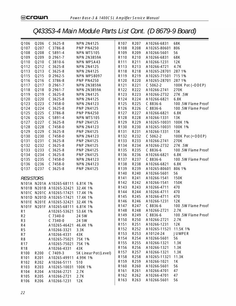
Q43353-4 Main Module Parts List Cont. (D 8679-9 Board)
Q106 Q206 C 3625-8 NPN 2N4125Q107 Q207 C 3786-8 PNP PN4250Q108 Q208 C 5891-4 NPN MTS105Q109 Q209 D 2961-7 NPN 2N3859AQ110 Q210 C 3810-6 NPN MPSA43Q112 Q212 C 3625-8 NPN 2N4125Q113 Q213 C 3625-8 NPN 2N4125Q115 Q215 D 2962-5 NPN MPS8097Q116 Q216 C 3786-8 PNP PN4250Q117 Q217 D 2961-7 NPN 2N3859AQ118 Q218 D 2961-7 NPN 2N3859AQ119 Q219 C 3625-8 NPN 2N4125Q120 Q220 C 3625-8 NPN 2N4125Q123 Q223 C 7458-0 NPN 2N4123Q124 Q224 C 3625-8 PNP 2N4125Q125 Q225 C 3786-8 PNP PN4250Q126 Q226 C 5891-4 NPN MTS105Q127 Q227 C 3625-8 PNP 2N4125Q128 Q228 C 7458-0 NPN 2N4123Q129 Q229 C 3625-8 PNP 2N4125Q130 Q230 C 7458-0 NPN 2N4123Q131 Q231 C 3625-8 PNP 2N4125Q132 Q232 C 3625-8 PNP 2N4125Q133 Q233 C 3625-8 PNP 2N4125Q134 Q234 C 3625-8 PNP 2N4125Q135 Q235 C 7458-0 NPN 2N4123Q136 Q236 C 7458-0 NPN 2N4123Q137 Q237 C 3625-8 PNP 2N4125
RESISTORSN101A N201A A10265-68111 6.81K 1%N101B N201B A10265-32421 32.4K 1%N101C N201C A10265-17421 17.4K 1%N101D N201D A10265-17421 17.4K 1%N101E N201E A10265-32421 32.4K 1%N101F N201F A10265-68111 6.81K 1%R1 A10265-53621 53.6K 1%R2 C 7340-0 24 5WR3 C 7340-0 24 5WR4 A10265-46421 46.4K 1%R5 A10266-3321 3.3KR7 A10266-4331 43KR8 A10265-75021 75K 1%R17 A10265-75021 75K 1%R18 A10266-4331 43KR100 R200 C 7409-3 5K Linear Pot (Level)R101 R201 A10265-49911 4.99K 1%R102 R202 A10266-5111 510R103 R203 A10265-10031 100K 1%R104 R204 A10266-2721 2.7KR105 R205 A10266-2721 2.7KR106 R206 A10266-1231 12K
R107 R207 A10266-6831 68KR108 R208 A10265-80601 806R109 R209 A10266-5601 56R110 R210 A10266-6831 68KR111 R211 A10266-1231 12KR113 R213 A10266-4721 4.7KR118 R218 A10265-28701 287 1%R119 R219 A10265-71501 715 1%R120 R220 A10265-28701 287 1%R121 R221 C 5062-2 100K Pot (–ODEP)R122 R222 A10266-2741 270KR123 R223 A10266-2732 27K .5WR124 R224 A10266-6821 6.8KR125 R225 C 8836-6 100 .5W Flame ProofR126 R226 C 8836-6 100 .5W Flame ProofR127 R227 A10266-6821 6.8KR128 R228 A10266-1331 13KR129 R229 A10265-10031 100K 1%R130 R230 A10265-10031 100K 1%R131 R231 A10266-1331 13KR132 R232 C 5062-2 100K Pot (+ODEP)R133 R233 A10266-2741 270KR134 R234 A10266-2732 27K .5WR135 R235 C 8836-6 100 .5W Flame ProofR136 R236 A10266-6821 6.8KR137 R237 C 8836-6 100 .5W Flame ProofR138 R238 A10266-6821 6.8KR139 R239 A10265-80601 806 1%R140 R240 A10266-5601 56R141 R241 A10266-1541 150KR142 R242 A10266-1541 150KR143 R243 A10266-4711 470R144 R244 A10266-4711 470R145 R245 A10266-4711 470R146 R246 A10266-1231 12KR147 R247 C 8836-6 100 .5W Flame ProofR148 R248 A10266-2721 2.7KR149 R249 C 8836-6 100 .5W Flame ProofR150 R250 A10266-2721 2.7KR151 R251 A10266-1231 12KR152 R252 A10265-11521 11.5K 1%R153 R253 A10124-24 JUMPERR154 R254 A10266-5601 56R155 R255 A10266-1321 1.3KR156 R256 A10266-1321 1.3KR157 R257 A10266-1321 1.3KR158 R258 A10265-11321 11.3KR159 R259 A10266-1021 1KR160 R260 A10266-5601 56R161 R261 A10266-4701 47R162 R262 A10266-4701 47R163 R263 A10266-5601 56
Power Base-3 & 1400CSL Amplifier Service Manual
23
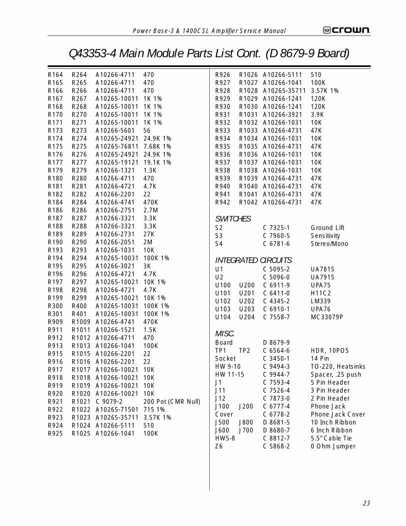
Q43353-4 Main Module Parts List Cont. (D 8679-9 Board)
R164 R264 A10266-4711 470R165 R265 A10266-4711 470R166 R266 A10266-4711 470R167 R267 A10265-10011 1K 1%R168 R268 A10265-10011 1K 1%R170 R270 A10265-10011 1K 1%R171 R271 A10265-10011 1K 1%R173 R273 A10266-5601 56R174 R274 A10265-24921 24.9K 1%R175 R275 A10265-76811 7.68K 1%R176 R276 A10265-24921 24.9K 1%R177 R277 A10265-19121 19.1K 1%R179 R279 A10266-1321 1.3KR180 R280 A10266-4711 470R181 R281 A10266-4721 4.7KR182 R282 A10266-2201 22R184 R284 A10266-4741 470KR186 R286 A10266-2751 2.7MR187 R287 A10266-3321 3.3KR188 R288 A10266-3321 3.3KR189 R289 A10266-2731 27KR190 R290 A10266-2051 2MR193 R293 A10266-1031 10KR194 R294 A10265-10031 100K 1%R195 R295 A10266-3021 3KR196 R296 A10266-4721 4.7KR197 R297 A10265-10021 10K 1%R198 R298 A10266-4721 4.7KR199 R299 A10265-10021 10K 1%R300 R400 A10265-10031 100K 1%R301 R401 A10265-10031 100K 1%R909 R1009 A10266-4741 470KR911 R1011 A10266-1521 1.5KR912 R1012 A10266-4711 470R913 R1013 A10266-1041 100KR915 R1015 A10266-2201 22R916 R1016 A10266-2201 22R917 R1017 A10266-10021 10KR918 R1018 A10266-10021 10KR919 R1019 A10266-10021 10KR920 R1020 A10266-10021 10KR921 R1021 C 9079-2 200 Pot (CMR Null)R922 R1022 A10265-71501 715 1%R923 R1023 A10265-35711 3.57K 1%R924 R1024 A10266-5111 510R925 R1025 A10266-1041 100K
R926 R1026 A10266-5111 510R927 R1027 A10266-1041 100KR928 R1028 A10265-35711 3.57K 1%R929 R1029 A10266-1241 120KR930 R1030 A10266-1241 120KR931 R1031 A10266-3921 3.9KR932 R1032 A10266-1031 10KR933 R1033 A10266-4731 47KR934 R1034 A10266-1031 10KR935 R1035 A10266-4731 47KR936 R1036 A10266-1031 10KR937 R1037 A10266-1031 10KR938 R1038 A10266-1031 10KR939 R1039 A10266-4731 47KR940 R1040 A10266-4731 47KR941 R1041 A10266-4731 47KR942 R1042 A10266-4731 47K
SWITCHESS2 C 7325-1 Ground LiftS3 C 7960-5 SensitivityS4 C 6781-6 Stereo/Mono
INTEGRATED CIRCUITSU1 C 5095-2 UA7815U2 C 5096-0 UA7915U100 U200 C 6911-9 UPA75U101 U201 C 6411-0 H11C2U102 U202 C 4345-2 LM339U103 U203 C 6910-1 UPA76U104 U204 C 7558-7 MC33079P
MISC.Board D 8679-9TP1 TP2 C 6564-6 HDR, 10POSSocket C 3450-1 14 PinHW 9-10 C 9494-3 TO-220, HeatsinksHW 11-15 C 9944-7 Spacer, .25 pushJ1 C 7593-4 5 Pin HeaderJ11 C 7526-4 3 Pin HeaderJ12 C 7873-0 2 Pin HeaderJ100 J200 C 6777-4 Phone JackCover C 6778-2 Phone Jack CoverJ500 J800 D 8681-5 10 Inch RibbonJ600 J700 D 8680-7 6 Inch RibbonHW5-8 C 8812-7 5.5" Cable TieZ6 C 5868-2 0 Ohm Jumper
Power Base-3 & 1400CSL Amplifier Service Manual
24
Q43400-3 PB-3, 1400CSL MAIN MODULE
CAPACITORSC1 C 3913-8 470µFC2 C 3913-8 470µFC4 C 6802-0 .47µFC5 C 6806-1 .01µFC6 C 6806-1 .01µFC7 C 8897-8 .1µFC8 C 5362-6 2.2uFC100 C200 C 5311-3 22µFC101 C201 C 9464-6 10pFC102 C202 C 8576-8 100uFC103 C203 C 6805-3 .022µFC104 C204 C 6805-3 .022µFC105 C205 C 6812-9 47pFC106 C206 C 6812-9 47pFC107 C207 C 8897-8 .1µFC108 C208 C 6814-5 12pFC109 C209 C 8576-8 100µFC110 C210 C 5362-6 2.2µFC112 C212 C 9991-8 1µFC113 C213 C 9992-6 47µFC114 C214 C 8854-9 100µFC115 C215 C 8854-9 100µFC116 C216 C 9992-6 47µFC117 C217 C 9991-8 1µFC118 C218 C 6814-5 12pFC119 C219 C 6802-0 .47µFC122 C222 C 6811-1 100pFC123 C223 C 6812-9 47pFC124 C224 C 6812-9 47pFC129 C229 C 6814-5 12pFC130 C230 C 6813-7 27pFC133 C233 C 6813-7 27pFC134 C234 C 6805-3 .022µFC135 C235 C 6805-3 .022µFC136 C236 C 6808-7 470pFC137 C237 C 6808-7 470pFC138 C238 C 6813-7 27pFC139 C239 C 6813-7 27pFC140 C240 C 6812-9 47pFC141 C241 C 6812-9 47pFC144 C244 C 8576-8 100µFC145 C245 C 6812-9 47pFC146 C246 C 6812-9 47pFC147 C247 C 6806-1 .01µFC148 C248 C 6810-3 180pFC149 C249 C 6808-7 470pFC150 C250 C 6806-1 .01µFC151 C251 C 6806-1 .01µFC152 C252 C 6950-7 82pF 5%
Q43400-3 Main Module Parts List (D 8827-4)
C153 C253 C 8897-8 .1µFC154 C254 A10434-104JD .1µF 250VC155 C255 C 8897-8 .1µFC156 C256 C 8897-8 .1µFC158 C258 C 6805-3 .022uFC159 C259 C 6805-3 .022uFC160 C260 C 8897-8 .1uFC161 C261 C 8897-8 .1uFC113X C213X OPENC116X C216X OPEN
DIODESD1 C 2851-1 1N4004D2 C 2851-1 1N4004D3 C 2851-1 1N4004D4 C 2851-1 1N4004D5 C 2851-1 1N4004D6 C 2851-1 1N4004D7 C 2851-1 1N4004D100 D200 C 3181-2 1N4148D101 D201 C 3181-2 1N4148D102 D202 C 3824-7 1N970BD103 D203 C 3181-2 1N4148D104 D204 C 3181-2 1N4148D105 D205 C 2851-1 1N4004D106 D206 C 2851-1 1N4004D108 D208 C 3181-2 1N4148D109 D209 C 3181-2 1N4148D110 D210 C 3181-2 1N4148D111 D211 C 5061-4 1N3070D112 D212 C 3181-2 1N4148D113 D213 C 3181-2 1N4148D120 D220 C 3181-2 1N4148D121 D221 C 3181-2 1N4148D122 D222 C 3181-2 1N4148D123 D223 C 5061-4 1N3070D124 D224 C 3181-2 1N4148D125 D225 C 3181-2 1N4148D126 D226 C 5061-4 1N3070D127 D227 C 5061-4 1N3070D128 228 OPEND129 D229 C 3181-2 1N4148D130 D230 C 3181-2 1N4148D131 D231 C 3181-2 1N4148D132 D232 C 3181-2 1N4148D133 D233 C 3181-2 1N4148D134 D234 C 3181-2 1N4148
L.E.D.'SE100 E200 C 9857-1 REDE101 E201 C 9857-1 RED
Power Base-3 & 1400CSL Amplifier Service Manual
25
NETWORK RESISTORSN101A N201A A10265-68111 6.81K 1%N101B N201B A10265-32421 32.4K 1%N101C N201C A10265-17421 17.4K 1%N101D N201D A10265-17421 17.4K 1%N101E N201E A10265-32421 32.4K 1%N101F N201F A10265-68111 6.81K 1%
TRANSISTORSQ100 Q200 D 2961-7 2N3859AQ101 Q201 C 3578-9 MPSA93Q102 Q202 C 3810-6 MPSA43Q103 Q203 C 3786-8 PN4250Q105 Q205 C 3578-9 MPSA93Q106 Q206 C 3625-8 2N4125Q107 Q207 C 3786-8 PN4250Q108 Q208 C 5891-4 MTS105Q109 Q209 D 2961-7 2N3859AQ110 Q210 C 3810-6 MPSA43Q112 Q212 C 3625-8 2N4125Q113 Q213 C 3625-8 2N4125Q115 Q215 D 2962-5 MPS8097Q116 Q216 C 3786-8 PN4250Q117 Q217 D 2961-7 2N3859AQ118 Q218 D 2961-7 2N3859AQ119 Q219 C 3625-8 2N4125Q120 Q220 C 3625-8 2N4125Q123 Q223 C 7458-0 2N4123Q124 Q224 C 3625-8 2N4125Q125 Q225 C 3786-8 PN4250Q126 Q226 C 5891-4 MTS105Q127 Q227 C 3625-8 2N4125Q128 Q228 C 7458-0 2N4123Q129 Q229 C 3625-8 2N4125Q130 Q230 C 7458-0 2N4123Q131 Q231 C 3625-8 2N4125Q132 Q232 C 3625-8 2N4125Q133 Q233 C 3625-8 2N4125Q134 Q234 C 3625-8 2N4125Q135 Q235 C 7458-0 2N4123Q136 Q236 C 7458-0 2N4123Q137 Q237 C 3625-8 2N4125Q138 Q238 C 3810-6 MPSA42Q139 Q239 C 3578-9 MPSA93
RESISTORSR1 A10265-53621 53.6K 1%R2 C 7340-0 24 5WR3 C 7340-0 24 5WR4 A10265-46421 46.4K 1%R5 C 3617-5 3.3K 1W
Q43400-3 Main Module Parts List Cont. (D 8827-4)
R7 A10266-4331 43KR8 A10265-75021 75K 1%R10 OPENR11 OPENR12 OPENR17 A10265-75021 75K 1%R18 A10266-4331 43KR100 R200 C 7409-3 5K Linear PotR101 R201 A10265-49911 4.99K 1%R102 R202 A10266-5111 510R103 R203 A10265-10031 100K 1%R104 R204 A10266-2721 2.7KR105 R205 A10266-2721 2.7KR106 R206 A10266-1231 12KR107 R207 A10266-6831 68KR108 R208 A10265-80601 806R109 R209 A10266-5601 56R110 R210 A10266-6831 68KR111 R211 A10266-1231 12KR112 R212 OPENR113 R213 A10266-4721 4.7KR114 R214 OPENR115 R215 OPENR116 R216 OPENR117 R217 OPENR118 R218 A10265-28701 287 1%R119 R219 A10265-71501 715 1%R120 R220 A10265-28701 287 1%R121 R221 C 5062-2 100K PotR122 R222 A10266-2741 270KR123 R223 A10266-2732 27K .5WR124 R224 A10266-6821 6.8KR125 R225 C 8836-6 100 .5W FPR126 R226 C 8836-6 100 .5W FPR127 R227 A10266-6821 6.8KR128 R228 A10266-1331 13KR129 R229 A10265-10031 100K 1%R130 R230 A10265-10031 100K 1%R131 R231 A10266-1331 13KR132 R232 C 5062-2 100K PotR133 R233 A10266-2741 270KR134 R234 A10266-2732 27K .5WR135 R235 C 8836-6 100 .5W FPR136 R236 A10266-6821 6.8KR137 R237 C 8836-6 100 .5W FPR138 R238 A10266-6821 6.8KR139 R239 A10265-80601 806 1%R140 R240 A10266-5601 56R141 R241 A10266-1541 150KR142 R242 A10266-1541 150KR143 R243 A10266-4711 470R144 R244 A10266-4711 470
Power Base-3 & 1400CSL Amplifier Service Manual
26
R145 R245 A10266-4711 470R146 R246 A10266-1231 12KR147 R247 C 8836-6 100 .5W FPR148 R248 A10266-2721 2.7KR149 R249 C 8836-6 100 .5W FPR150 R250 A10266-2721 2.7KR151 R251 A10266-1231 12KR152 R252 A10265-11521 11.5K 1%R153 R253 A10124-24 JUMPERR154 R254 A10266-5601 56R155 R255 A10266-1321 1.3KR156 R256 A10266-1321 1.3KR157 R257 A10266-1321 1.3KR158 R258 A10265-11321 11.3KR159 R259 A10265-10011 1K 1%R160 R260 A10266-5601 56R161 R261 A10266-4701 47R162 R262 A10266-4701 47R163 R263 C10166-4 56 FPR164 R264 A10266-4711 470R165 R265 A10266-4711 470R166 R266 A10266-4711 470R167 R267 A10265-10011 1K 1%R168 R268 A10265-10011 1K 1%R169 R269 OPENR170 R270 A10265-10011 1K 1%R171 R271 A10265-10011 1K 1%R172 R272 OPENR173 R273 C10166-4 56 FPR174 R274 A10265-24921 24.9K 1%R175 R275 A10265-80611 8.06K 1%R176 R276 A10265-24921 24.9K 1%R177 R277 A10265-20021 20.0K 1%R179 R279 A10266-1321 1.3KR180 R280 A10266-4711 470R181 R281 A10266-4721 4.7KR182 R282 A10266-2201 22R184 R284 A10266-4741 470KR186 R286 A10266-2751 2.7MR187 R287 A10266-3321 3.3KR188 R288 A10266-3321 3.3KR189 R289 A10266-2731 27KR190 R290 A10266-2051 2MR193 R293 A10266-1031 10KR194 R294 A10265-10031 100K 1%R195 R295 A10266-3021 3KR196 R296 A10266-4721 4.7KR197 R297 A10265-10021 10K 1%R198 R298 A10266-4721 4.7KR199 R299 A10265-10021 10K 1%R300 R400 A10265-10031 100K 1%R301 R401 A10265-10031 100K 1%
Q43400-3 Main Module Parts List Cont. (D 8827-4)
R911 R1011 A10266-1521 1.5KR912 R1012 A10266-4711 470R913 R1013 A10266-1041 100KR914 R1014 OPENR915 R1015 A10266-2201 22R916 R1016 A10266-2201 22R917 R1017 A10266-10021 10KR918 R1018 A10266-10021 10KR919 R1019 A10266-10021 10KR920 R1020 A10266-10021 10KR921 R1021 C 9079-2 200 PotR922 R1022 A10265-71501 715 1%R923 R1023 A10265-35711 3.57K 1%R924 R1024 A10266-5111 510R925 R1025 A10266-1041 100KR926 R1026 A10266-5111 510R927 R1027 A10266-1041 100KR928 R1028 A10265-35711 3.57K 1%R929 R1029 A10266-1241 120KR930 R1030 A10266-1241 120KR931 R1031 A10266-3921 3.9KR932 R1032 A10266-1031 10KR933 R1033 A10266-4731 47KR934 R1034 A10266-1031 10KR935 R1035 A10266-4731 47KR936 R1036 A10266-1031 10KR937 R1037 A10266-1031 10KR938 R1038 A10266-1031 10KR939 R1039 A10266-4731 47KR940 R1040 A10266-4731 47KR941 R1041 A10266-4731 47KR942 R1042 A10266-4731 47KR943 R1043 A10266-1031 10KR944 R1044 A10266-1031 10KR945 R1045 A10266-4701 47R946 R1046 A10266-2031 20KR947 R1074 A10266-2031 20K
SWITCHESS2 C 7325-1 Ground LiftS3 C 7960-5 SensitivityS4 C 6781-6 Stereo/Mono
HEADERSTP1 TP2 C 6564-6 HDR
INTEGRATED CIRCUITSU1 C 5095-2 UA7815U2 C 5096-0 UA7915U100 U200 C 6911-9 UPA75U101 U201 C 6411-0 H11C2
Power Base-3 & 1400CSL Amplifier Service Manual
27
Q43400-3 Main Module Parts List Cont. (D 8827-4)
U102 U202 C 4345-2 LM339U103 U203 C 6910-1 UPA76U104 U204 C 7558-7 MC33079PU100A U200A OPENU103A U203A OPEN
MISCELLANEOUSBoard D 8827-4Socket C 3450-1 14 Pin, (2)HW9-10 C 9494-3 TO-220, (2)HW11-15 C 9944-7 Spacer, (5)J1 C 7593-4 5 Pin HDRJ2 OPENJ11 C 7526-4 3 Pin HDRJ12 C 7873-0 2 Pin HDRJ100 J200 C 6777-4 Input, Ph JkCover C 6778-2 Ph Jk CVRJ101 J201 OPENJ500 J800 D 8681-5 Ribbon, 10"J600 J700 D 8680-7 Ribbon, 6"HW5-8 C 8812-7 5.5" Tie, (4)Z6 C 5868-2 0 Ohm Jmp