Embed Size (px)
Citation preview
16
Contact Definition in Industrial Silicon Solar Cells
Dr. Luis Jaime Caballero Isofoton S.A.
Spain
1. Introduction
The incredible development that industrial silicon based photovoltaic devices have followed for the last decades has been related to the consecution of a simple, easy and economically feasible way to define the electrical contacts of the devices. Due to the size of silicon photovoltaic device in relation to its substrate wafer size (one device per wafer), traditional microelectronic means to define contact (using metal evaporation in vacuum and photolithographic processes) are not economically appropriate for the mass production devices. Screen-printing technique has represented the perfect means to allow the production cost reduction, and the strong introduction of photovoltaic devices for terrestrial applications in the global market. Although similar primitive printing techniques have been known by the mankind thousand
of years ago, the industrial introduction of the screen-printing technique had to wait till the
end of the XIX century, beginning of the XX century. Its application in the textile industry
started the beginning of its intensive use. It was in the second half of the XX century when
electronic industry started to employ this technique in the field of the hybrid circuits for the
deposition of dielectric and conductive layers; but its first applications in the photovoltaic
industry dates from 1975-6 (Ralph, 1975); (Haigh, 1976). Since then, improvements of the
screen-printing techniques and metal pastes for the creation of contacts have been crucial for
the development and improvement that industrial produced silicon solar cells have
followed, becoming the heart of its fabrication processes.
But the technical characteristics of the screen-printed contacts are far from the ones obtained
when a metal is deposited on the silicon surface with a microelectronic process in vacuum
conditions, introducing limitations to the final energy conversion efficiency that devices can
reach. The strong interest in increasing the conversion efficiency of industrial solar cells is
encouraging the appearance of new research focused on overcoming this limitations. For
this reason, advances and new developments in other techniques seem to be the future way
to get improved contacts in mass production device fabrication. The application of these
could mean changes in the nowadays standard processing technology that would be
introduced by the industry in coming years.
This chapter aims to present the curent contact definition technique, reviewing the screen-printing technology, and the ways followed to optimize its results, getting higher conversion efficiencies in devices; some design topics for the front grid patterns will be
Source: Solar Energy, Book edited by: Radu D. Rugescu, ISBN 978-953-307-052-0, pp. 432, February 2010, INTECH, Croatia, downloaded from SCIYO.COM
www.intechopen.com
Solar Energy
376
discussed, finishing with a quick introductory view on the future of the industrial silicon solar cell with special attention to its contact definition.
2. Screen printing of metallic contacts basic fundamentals
The screen printing process consists in the transference of an ink or paste (with a specific viscosity) through a screen that allows its pass in a defined pattern, thanks to the pressure applied by a squeegee fixed in a moving part. Basic parts of a system for a solar cell screen-printing definition process are:
• The screen, comprising a frame that holds a stretched fabric with a photo stencil attached to the mesh with the required design of the grid pattern.
• A squeegee, comprising a holder with a fixed, flexible, resilient blade.
• A metallic conductive paste that is transferred to the device surface,
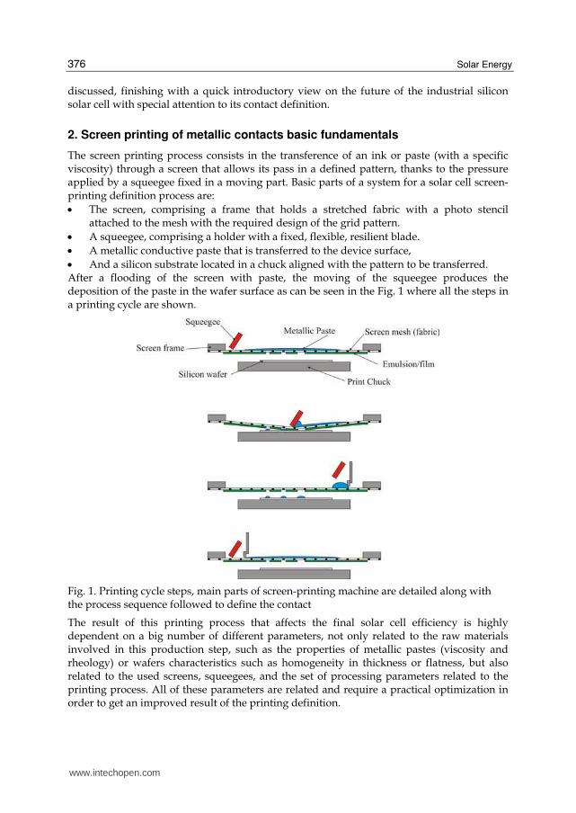
• And a silicon substrate located in a chuck aligned with the pattern to be transferred. After a flooding of the screen with paste, the moving of the squeegee produces the deposition of the paste in the wafer surface as can be seen in the Fig. 1 where all the steps in a printing cycle are shown.
Fig. 1. Printing cycle steps, main parts of screen-printing machine are detailed along with the process sequence followed to define the contact
The result of this printing process that affects the final solar cell efficiency is highly dependent on a big number of different parameters, not only related to the raw materials involved in this production step, such as the properties of metallic pastes (viscosity and rheology) or wafers characteristics such as homogeneity in thickness or flatness, but also related to the used screens, squeegees, and the set of processing parameters related to the printing process. All of these parameters are related and require a practical optimization in order to get an improved result of the printing definition.
www.intechopen.com
Contact Definition in Industrial Silicon Solar Cells
377
It can be said that the more homogeneous the device structure (in the whole surface area), the more efficient the final solar cell. Therefore a homogeneous definition of the front contact is important in order to get an optimal industrial solar cell. Among the processing parameter are the pressure applied by the squeegee, the speed of its
printing movement and the related position of the wafer surface with respect to the screen
position. While among the parameter related with the screens that define the pattern, it can
be found the material of the fabric (typically stain-steel due to its good response for mass
production), its constituent wires’ diameter and mesh density (wires per centimetre), the
thickness of the fabric, its attached emulsion or film, and the stretching of the mesh of the
screen.
All this set of parameters and its effects (studied early in the literature of the thick film technology field (Holmes & Loasby, 1976)) makes the printing a complex process to be optimised, which must be analysed on the industrial environment with the help of statistical tools based in the final device performance, and the optical and electrical characterization of the final contact definition of the produced solar cells; always inside specific designs of experiments where parameter are changed in defined working ranges (using a DOE analysis tool).
3. Composition of metallic pastes
3.1 Front paste composition Metallic contact nowadays employed by the industry are based on the use of silver as a conductive metal due to its good contact properties with n type silicon, its good conductivity and its excellent solderability (needed for the later interconnection of cells). To make the deposition of this metallic contact with a screenprinting technique possible, with the goal of reaching a final correct mechanical adhesion to the surfaces and good electrical properties, special metallic pastes have been developed for the solar cell industry. Silver powder represents the 70-85% in weight of the commercial pastes with a mixture of different shaped particles, of different sizes (as spherical powder grains or flakes), that are responsible for the paste conductivity and final cohesion of the contact. The rest of the paste components are extremely sensitive to the device surface that want to be contacted (with different dielectrics layers of different thickness that pastes must go through), and to the specific processing of contact creations such as temperature profiles and processing times. These are:
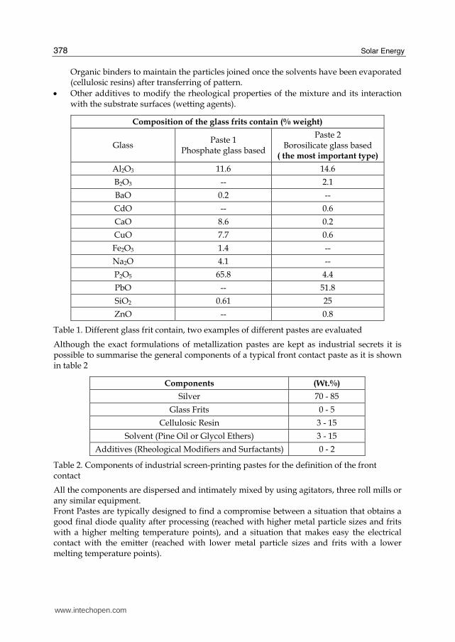
• Powder of glass frits. Glass frits are metal oxides that play the most important role in the formation of the contact because its function is to melt the dielectric layers (by forming eutectic alloys of lower melting point), that are deposited or grown on the silicon emitter, allowing the metal particles to reach the silicon surface. Additionally its content determines the adhesion of the paste to the silicon substrate. An example of the different glass frits contain of two pastes is shown in Table 1 (Firor & Hogan, 1981)
• Organic compounds used as a vehicle to transport the suspended silver and glass particles, allowing its disposal with the screen printing techniques. Among these organic compounds are: Organic solvent to allow the mixture to be used as a paint, and
www.intechopen.com
Solar Energy
378
Organic binders to maintain the particles joined once the solvents have been evaporated (cellulosic resins) after transferring of pattern.
• Other additives to modify the rheological properties of the mixture and its interaction with the substrate surfaces (wetting agents).
Composition of the glass frits contain (% weight)
Glass Paste 1
Phosphate glass based
Paste 2 Borosilicate glass based
( the most important type)
Al2O3 11.6 14.6
B2O3 -- 2.1
BaO 0.2 --
CdO -- 0.6
CaO 8.6 0.2
CuO 7.7 0.6
Fe2O3 1.4 --
Na2O 4.1 --
P2O5 65.8 4.4
PbO -- 51.8
SiO2 0.61 25
ZnO -- 0.8
Table 1. Different glass frit contain, two examples of different pastes are evaluated
Although the exact formulations of metallization pastes are kept as industrial secrets it is possible to summarise the general components of a typical front contact paste as it is shown in table 2
Components (Wt.%)
Silver 70 - 85
Glass Frits 0 - 5
Cellulosic Resin 3 - 15
Solvent (Pine Oil or Glycol Ethers) 3 - 15
Additives (Rheological Modifiers and Surfactants) 0 - 2
Table 2. Components of industrial screen-printing pastes for the definition of the front contact
All the components are dispersed and intimately mixed by using agitators, three roll mills or any similar equipment. Front Pastes are typically designed to find a compromise between a situation that obtains a good final diode quality after processing (reached with higher metal particle sizes and frits with a higher melting temperature points), and a situation that makes easy the electrical contact with the emitter (reached with lower metal particle sizes and frits with a lower melting temperature points).
www.intechopen.com
Contact Definition in Industrial Silicon Solar Cells
379
3.2 Rear paste composition As for the front contact, the rear contact is also deposited by screen-printing techniques in nowadays industrial solar cells. In this case, as the type of silicon that must be contacted is p, the metal that constitutes the paste for the rear contact is Aluminium instead of Silver. But due to the problems of solderability that this material presents, with the formation of its surface oxide, industrial definition of the rear contact is carried out with a double step printing that defines:
• First the area that will be used, later on, to bond the connection ribbons (tabs), using a paste based on silver or silver and aluminium mixtures;
• And a second printing process that must be aligned with the first, with a paste based on aluminium particles to create the rear structure of the industrial solar cells knows as bsf (back surface field), due to the electrical field that aluminium doping generates in the silicon bulk near the surface.
Apart from the different metal particles of this pastes, the rest of the components that constitutes the final mixture are more or less the same because frits to improve adhesion and to remove residual dielectric layers, that can appear due to processing, are also needed, although in a lesser extend.
3.3 Supplied pastes properties Among the parameters typically reported by the paste suppliers it is possible to find:
• The ‘Viscosity’, whose characterization should report the measured value along with equipment used to measure viscosity (spindle or cone/plate) and temperature.
• Possible 'Thinners’ that are listed in the event of needed viscosity adjustments.
• The ‘Solids Content’ that is reported for combined inorganic content (in absence of organic) and ‘Metal Content’.
• The ‘Fineness of Grind’ (FOG) that is reported for the first scratch (≤).
• Some after processing parameters such as: the ‘Dried Thickness’ and ‘Fired Thickness’ that are given as a range reported in μm, and the ‘Resistivity’ (for a fired thickness given in mΩ/square).
• Some processing parameters such as the ‘Drying Profile’ giving applicable ranges and necessary durations, the ‘Peak temperature’ that gives the optimal firing range, the ‘Peak Duration’ reporting the optimal value or a range and the ‘Firing Atmosphere’ that is typically air.
• And other supplied parameters such as the ‘Shelf Life’ of the paste that is listed for a properly sealed container.
4. Contact formation, the co-firing process
As both contacts of solar cells are nowadays deposited using the same technique, pastes are designed to follow a common thermal final treatment that creates the contact in both faces of the cell. This process is called ‘co-firing’ and industrially is carried out with in-line belt furnaces in a (typically) air atmosphere during processing. The sequence to produce the final cell structure is:
• Printing of the front (silver) contact
• Drying of the front contact
• Printing of the back contact (aluminium contact with two printing processes as was introduced in previous section, with a drying process before the second printing process)
www.intechopen.com
Solar Energy
380
• Drying of the Back contact
• Co-firing process, to create the contact, and a
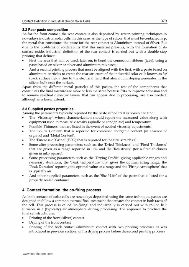
• Laser isolation process (if wafers have not been previously isolated chemically) It is important to keep the defined order in these steps to avoid any possible aluminium contamination of the front side of devices that would destroy the performance of the final cells (by creating a serious shunting problem of the p-n junction). During the co-firing process wafers follow a fast process with a defined temperature profile similar to the one that is shown in Fig. 2, resulting in chemical and structural changes inside the printed pastes and substrate surfaces.
Fig. 2. Temperature profile of the furnace for the co-firing process, and time of processing
The organic components that keep the dried metallic pastes attached to the surfaces are burn
out at the beginning of the process at temperatures below 600º C, step that is also used to
produce the diffusion of passivating hydrogen from the antireflective layer to the silicon
bulk. After this step the formation of the contact takes place at higher temperatures during
the firing peak. At this point glass frits (PbO-BO3-SiO2) melt the silicon nitride while silver
particles are transported through this melted mixture and suffer a sintering process that
creates a conductive film.
Liquid Pb generated during the chemical reaction etches the silicon surface in places where, during cooling, silver uses to recrystallize creating silver crystallites that are responsible for the ohmic contact with the emitter. After these steps the silver and glass frits mixture solidify creating a conductive contact that combines a direct contact between the sintered silver and the silver crystallites, a tunnelling contact through frits, and regions without electrical contact. On the other hand, at the rear surface aluminium paste follow the same burn out of organic
components as a first step. When temperature are above 660ºC the aluminium melt and can
go through the oxide that covers the particles (its oxide). The melted aluminium reaches the
silicon surface, and silicon is solved following the phase diagram of the Si-Al alloy. During
cooling down, silicon is rejected from the melt and recrystallize as an epitaxial Al-doped
layer creating a bsf.
When temperature are below 577ºC, the melted alloy solidify with the eutectic composition creating a layer whose contact with the silicon produces the typical bow of this aluminium bsf device structure.
www.intechopen.com
Contact Definition in Industrial Silicon Solar Cells
381
Controlling the bowing produced at the creation of the contact is one of the most important issues for the industry nowadays. The most extended technique to keep controlled the bowing is to control the weight of aluminium deposited through the weighting of the deposited paste (between 6 and 10 mg/cm2 of dried paste).
5. Practical industrial optimization of the metallization process
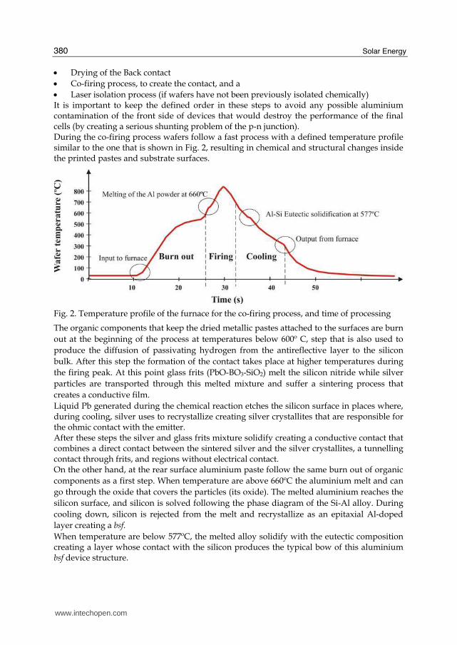
Industrial optimization of the firing process are carried out by means of a simplified DOE (Design of Experiment) that tries to find the optimal firing peak temperature for a specific thickness of substrates with a defined weight of rear aluminium paste deposited, once the wafers are right printed, and pastes are dried (in-line furnaces must be previously adjusted to ensure a perfect drying that eliminates many in other way existing problems). Fig. 3 shows the typical shape of the optimal metallization process working window as a function of the processing speed (speed of the furnace belt) and the furnace firing zone temperature; the effect of the substrate thickness on the right working window and its orientation inside the furnace during processing is also shown.
Fig. 3. Optimal Firing working window variation, picture on the left shows the dependency of the thickness of substrates, while picture on the right shows that when the front side is put on the belt, higher firing peak temperatures are needed
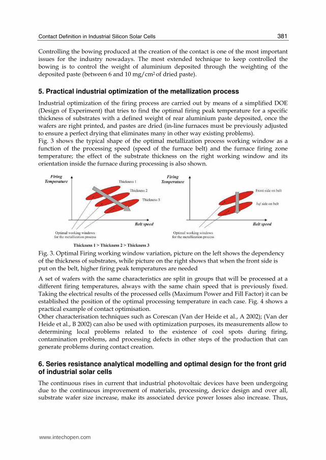
A set of wafers with the same characteristics are split in groups that will be processed at a different firing temperatures, always with the same chain speed that is previously fixed. Taking the electrical results of the processed cells (Maximum Power and Fill Factor) it can be established the position of the optimal processing temperature in each case. Fig. 4 shows a practical example of contact optimisation. Other characterisation techniques such as Corescan (Van der Heide et al., A 2002); (Van der Heide et al., B 2002) can also be used with optimization purposes, its measurements allow to determining local problems related to the existence of cool spots during firing, contamination problems, and processing defects in other steps of the production that can generate problems during contact creation.
6. Series resistance analytical modelling and optimal design for the front grid of industrial solar cells
The continuous rises in current that industrial photovoltaic devices have been undergoing due to the continuous improvement of materials, processing, device design and over all, substrate wafer size increase, make its associated device power losses also increase. Thus,
www.intechopen.com
Solar Energy
382
Fig. 4. Firing process optimization, example of a firing optimization attending to the final Fill Factor of resulting cells processed with its bsf rear contact on the furnace belt during firing. Corescan analysis for each temperature is also shown
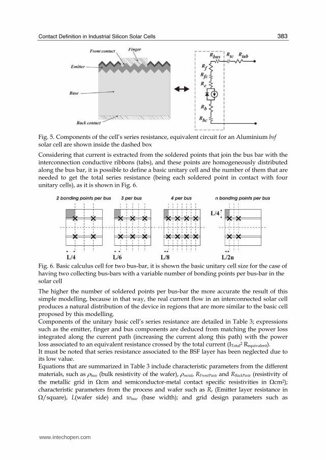
series resistance of cells that introduces this power loss constitutes a key factor that must be taken into account in order to reach higher energy conversion efficiencies. Series resistance components characterization and its associated power losses have a great importance in the cell and module fabrication field (Luque et al., 1986); (Roberts et al., 2000). It has a potential application in grid design, metallization paste research and development, solder or conductive adhesives contact resistance requirements, and number of solder points (Caballero et al., 2006) and interconnection ribbon thickness selection. Impact of the grid pattern design in the final series resistance of an industrial screen-printed silicon solar cell is known to be one of the strongest, so the correct design of the typical H pattern industrial front grids (a set of fingers orthogonal to two main collecting bus-bars) can improve the final device performance. This section will deal with this task, showing how it is possible to optimise the design of front grid through the use of an analytical modelling derived from the theoretical expressions of the power loss for each part of the device. The presented modelling will take into account only the contributions that compose the series resistance of a solar cell with total aluminium rear bsf, leaving out of this text the cell interconnection inside a module and the analysis of all the additional contributions to the module series resistance that can appear, just in order to get a simple reference tool for further future analysis.
6.1 Cell series resistance components When a cross-section of a simple cell is analysed it can be easily distinguished all the layers responsible for the different components of the series resistance, each one produces a power loss associated to the pass of the current through its volume. The total series resistance is the addition of all these components as it is plotted in the equivalent circuit of Fig. 5. The proposed analytical model calculate the series resistance of a square cell as the result of the parallel association of multiple unitary basic cells (neglecting the interconnection resistance between them) in which all the components of the series resistance are calculated.
www.intechopen.com
Contact Definition in Industrial Silicon Solar Cells
383
Fig. 5. Components of the cell’s series resistance, equivalent circuit for an Aluminium bsf solar cell are shown inside the dashed box
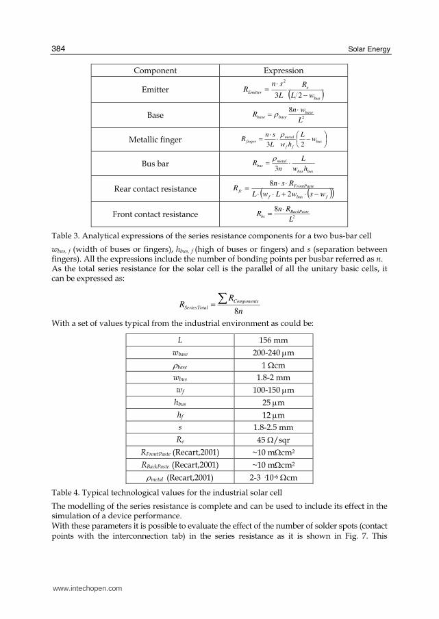
Considering that current is extracted from the soldered points that join the bus bar with the interconnection conductive ribbons (tabs), and these points are homogeneously distributed along the bus bar, it is possible to define a basic unitary cell and the number of them that are needed to get the total series resistance (being each soldered point in contact with four unitary cells), as it is shown in Fig. 6.
Fig. 6. Basic calculus cell for two bus-bar, it is shown the basic unitary cell size for the case of having two collecting bus-bars with a variable number of bonding points per bus-bar in the solar cell
The higher the number of soldered points per bus-bar the more accurate the result of this simple modelling, because in that way, the real current flow in an interconnected solar cell produces a natural distribution of the device in regions that are more similar to the basic cell proposed by this modelling. Components of the unitary basic cell’s series resistance are detailed in Table 3; expressions such as the emitter, finger and bus components are deduced from matching the power loss integrated along the current path (increasing the current along this path) with the power loss associated to an equivalent resistance crossed by the total current (ITotal2 Requivalent). It must be noted that series resistance associated to the BSF layer has been neglected due to its low value. Equations that are summarized in Table 3 include characteristic parameters from the different
materials, such as ρbase (bulk resistivity of the wafer), ρmetal, RFrontPaste and RBackPaste (resistivity of
the metallic grid in Ωcm and semiconductor-metal contact specific resistivities in Ωcm2); characteristic parameters from the process and wafer such as Re (Emitter layer resistance in
Ω/square), L(wafer side) and wbase (base width); and grid design parameters such as
www.intechopen.com
Solar Energy
384
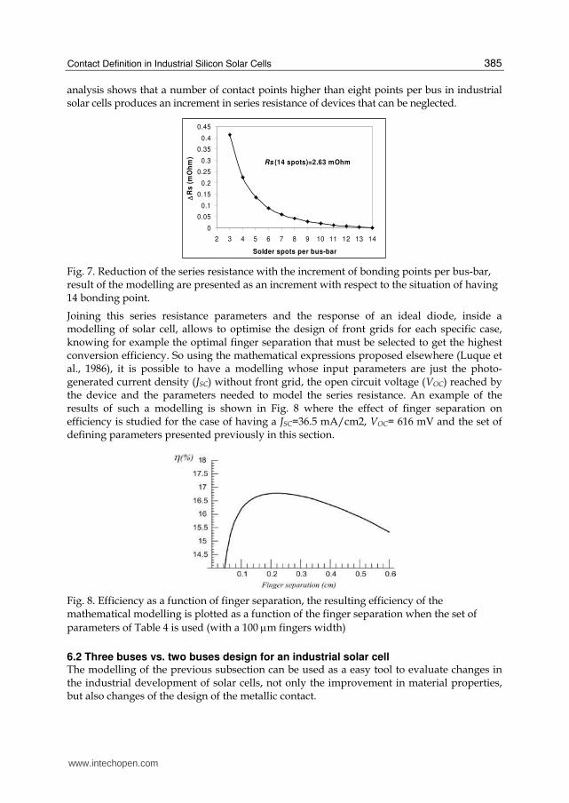
Component Expression
Emitter ( )bus
eEmitter
wL
R
L
snR −
⋅=23
2
Base 2
8
L
wnR base
basebase
⋅= ρ
Metallic finger ⎟⎠⎞⎜⎝
⎛ −⋅⋅= bus
ff
metalfinger w
L
hwL
snR
23
ρ
Bus bar busbus
metalbus
hw
L
nR ⋅=
3
ρ
Rear contact resistance ( )( )fbusf
FrontPastefc
wswLwL
RsnR −⋅+⋅⋅
⋅⋅=2
8
Front contact resistance 2
8
L
RnR BackPastebc
⋅=
Table 3. Analytical expressions of the series resistance components for a two bus-bar cell
wbus, f (width of buses or fingers), hbus, f (high of buses or fingers) and s (separation between fingers). All the expressions include the number of bonding points per busbar referred as n. As the total series resistance for the solar cell is the parallel of all the unitary basic cells, it can be expressed as:
n
RR
Components
TotalSeries8
∑=
With a set of values typical from the industrial environment as could be:
L 156 mm
wbase 200-240 μm
ρbase 1 Ωcm
wbus 1.8-2 mm
wf 100-150 μm
hbus 25 μm
hf 12 μm
s 1.8-2.5 mm
Re 45 Ω/sqr
RFrontPaste (Recart,2001) ~10 mΩcm2
RBackPaste (Recart,2001) ~10 mΩcm2
ρmetal (Recart,2001) 2-3 ·10-6 Ωcm
Table 4. Typical technological values for the industrial solar cell
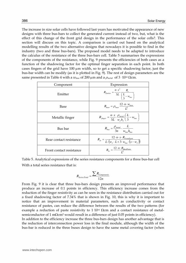
The modelling of the series resistance is complete and can be used to include its effect in the simulation of a device performance. With these parameters it is possible to evaluate the effect of the number of solder spots (contact points with the interconnection tab) in the series resistance as it is shown in Fig. 7. This
www.intechopen.com
Contact Definition in Industrial Silicon Solar Cells
385
analysis shows that a number of contact points higher than eight points per bus in industrial solar cells produces an increment in series resistance of devices that can be neglected.
0
0.05
0.1
0.15
0.2
0.25
0.3
0.35
0.4
0.45
2 3 4 5 6 7 8 9 10 11 12 13 14
Solder spots per bus-bar
ΔRs
(m
Oh
m)
Rs (14 spots)=2.63 mOhm
Fig. 7. Reduction of the series resistance with the increment of bonding points per bus-bar, result of the modelling are presented as an increment with respect to the situation of having 14 bonding point.
Joining this series resistance parameters and the response of an ideal diode, inside a modelling of solar cell, allows to optimise the design of front grids for each specific case, knowing for example the optimal finger separation that must be selected to get the highest conversion efficiency. So using the mathematical expressions proposed elsewhere (Luque et al., 1986), it is possible to have a modelling whose input parameters are just the photo-generated current density (JSC) without front grid, the open circuit voltage (VOC) reached by the device and the parameters needed to model the series resistance. An example of the results of such a modelling is shown in Fig. 8 where the effect of finger separation on efficiency is studied for the case of having a JSC=36.5 mA/cm2, VOC= 616 mV and the set of defining parameters presented previously in this section.
Fig. 8. Efficiency as a function of finger separation, the resulting efficiency of the mathematical modelling is plotted as a function of the finger separation when the set of
parameters of Table 4 is used (with a 100 μm fingers width)
6.2 Three buses vs. two buses design for an industrial solar cell The modelling of the previous subsection can be used as a easy tool to evaluate changes in the industrial development of solar cells, not only the improvement in material properties, but also changes of the design of the metallic contact.
www.intechopen.com
Solar Energy
386
The increase in size solar cells have followed last years has motivated the appearance of new designs with three bus-bars to collect the generated current instead of two, but, what is the effect of this change of the front grid design in the performance of the solar cells?. This section will discuss on this topic. A comparison is carried out based on the analytical modelling results of the two alternative designs that nowadays it is possible to find in the industry (two and three bus-bars). The proposed model needs to be adapted to introduce the calculus of the resistance of the three bus-bars cell. Table 5 summarises the expressions of the components of the resistance, while Fig. 9 presents the efficiencies of both cases as a function of the shadowing factor for the optimal finger separation in each point. In both
cases fingers of the grid have 100 μm width, so to get a specific shadowing factor, just the bus-bar width can be modify (as it is plotted in Fig. 9). The rest of design parameters are the
same presented in Table 4 with a wbase of 200 μm and a ρmetal of 3 ·10-6 Ωcm.
Component Expression
Emitter ⎟⎠⎞⎜⎝
⎛ −⋅=
bus
eEmitter
wL
R
L
snR
3
3
2
Base 2
12
L
wnR base
basebase
⋅⋅= ρ
Metallic finger ⎟⎠⎞⎜⎝
⎛ −⋅⋅= bus
ff
metalfinger w
L
hwL
snR
33
ρ
Bus bar busbus
metalbus
hw
L
nR ⋅=
3
ρ
Rear contact resistance ( )( )fbusf
FrontPastefc
wswLwL
RsnR −⋅⋅+⋅⋅
⋅⋅⋅=3
12
Front contact resistance 2
12
L
RnR BackPastebc
⋅⋅=
Table 5. Analytical expressions of the series resistance components for a three bus-bar cell
With a total series resistance that is:
n
RR
Components
TotalSeries12
∑=
From Fig. 9 it is clear that three bus-bars design presents an improved performance that produce an increase of 0.1 points in efficiency. This efficiency increase comes from the reduction of the finger resistivity as can be seen in the resistance distribution carried out for a fixed shadowing factor of 7.34% that is shown in Fig. 10, this is why it is important to notice that an improvement in material parameters, such as conductivity or contact resistance of pastes, can reduce the difference between the results of the two patterns (for
example a reduction of paste resistivity to 1·10-6 Ωcm and a contact resistance of metal-
semiconductor of 1 mΩcm2 would result in a difference of just 0.05 points in efficiency). In addition to the efficiency increase the three bus-bars design has another advantage that is the reduction of interconnection power loss in the final module, although the width of the bus-bar is reduced in the three buses design to have the same metal covering factor (when
www.intechopen.com
Contact Definition in Industrial Silicon Solar Cells
387
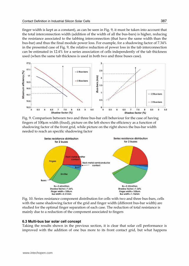
finger width is kept as a constant), as can be seen in Fig. 9, it must be taken into account that the total interconnection width (addition of the width of all the bus-bars) is higher, reducing the resistance associated to the tabbing interconnection (that have the same width than the bus-bar) and thus the final module power loss. For example, for a shadowing factor of 7.34% in the presented case of Fig. 9, the relative reduction of power loss in the tab interconnection can be estimated in 12.4% for a series association of cells independently of the tab thickness used (when the same tab thickness is used in both two and three buses case).
Fig. 9. Comparison between two and three bus-bar cell behaviour for the case of having
fingers of 100μm width (fixed), picture on the left shows the efficiency as a function of shadowing factor of the front grid, while picture on the right shows the bus-bar width needed to reach an specific shadowing factor
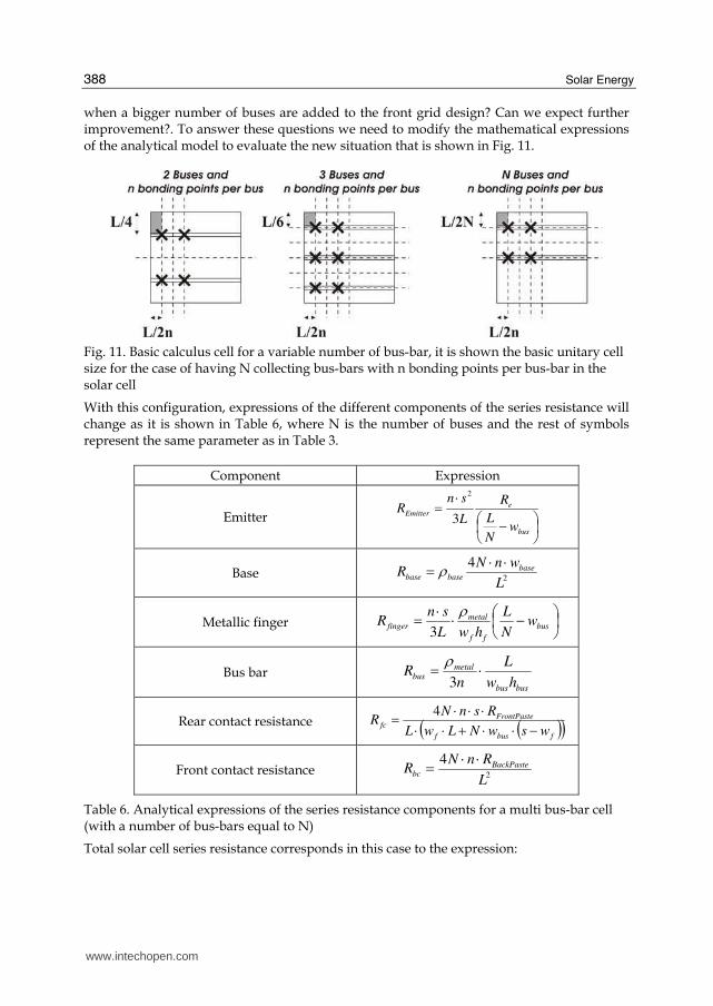
Fig. 10. Series resistance component distribution for cells with two and three bus-bars, cells with the same shadowing factor of the grid and finger width (different bus-bar width) are studied for the optimal finger separation of each case. The reduction of total resistance is mainly due to a reduction of the component associated to fingers
6.3 Multi-bus bar solar cell concept Taking the results shown in the previous section, it is clear that solar cell performance is improved with the addition of one bus more to its front contact grid, but what happens
www.intechopen.com
Solar Energy
388
when a bigger number of buses are added to the front grid design? Can we expect further improvement?. To answer these questions we need to modify the mathematical expressions of the analytical model to evaluate the new situation that is shown in Fig. 11.
Fig. 11. Basic calculus cell for a variable number of bus-bar, it is shown the basic unitary cell size for the case of having N collecting bus-bars with n bonding points per bus-bar in the solar cell
With this configuration, expressions of the different components of the series resistance will change as it is shown in Table 6, where N is the number of buses and the rest of symbols represent the same parameter as in Table 3.
Component Expression
Emitter ⎟⎠⎞⎜⎝
⎛ −⋅=
bus
eEmitter
wN
L
R
L
snR
3
2
Base 2
4
L
wnNR base
basebase
⋅⋅= ρ
Metallic finger ⎟⎠⎞⎜⎝
⎛ −⋅⋅= bus
ff
metalfinger w
N
L
hwL
snR
ρ3
Bus bar busbus
metalbus
hw
L
nR ⋅=
3
ρ
Rear contact resistance ( )( )fbusf
FrontPastefc
wswNLwL
RsnNR −⋅⋅+⋅⋅
⋅⋅⋅= 4
Front contact resistance 2
4
L
RnNR BackPastebc
⋅⋅=
Table 6. Analytical expressions of the series resistance components for a multi bus-bar cell (with a number of bus-bars equal to N)
Total solar cell series resistance corresponds in this case to the expression:
www.intechopen.com
Contact Definition in Industrial Silicon Solar Cells
389
Nn
RR
Components
TotalSeries ⋅= ∑4
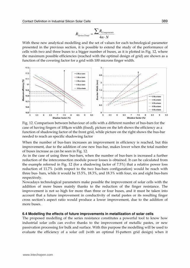
With these new analytical modelling and the set of values for each technological parameter presented in the previous section, it is possible to extend the study of the performance of cells with two and three buses to a bigger number of buses, as it is plotted in Fig. 12, where the maximum possible efficiencies (reached with the optimal design of grid) are shown as a function of the covering factor for a grid with 100 microns finger width.
Fig. 12. Comparison between behaviour of cells with a different number of bus-bars for the
case of having fingers of 100μm width (fixed), picture on the left shows the efficiency as a function of shadowing factor of the front grid, while picture on the right shows the bus-bar needed to reach an specific shadowing factor
When the number of bus-bars increases an improvement in efficiency is reached, but this improvement, due to the addition of one new bus-bar, makes lower when the total number of buses increase as can be seen in Fig. 12. As in the case of using three bus-bars, when the number of bus-bars is increased a further reduction of the interconnection module power losses is obtained. It can be calculated from the example referred in Fig. 12 (for a shadowing factor of 7.5%) that a relative power loss reduction of 11.7% (with respect to the two bus-bars configuration) would be reach with three bus- bars, while it would be 15.5%, 18.3%, and 18.3% with four, six and eight bus-bars respectively. Nowadays technological parameters make possible the improvement of solar cells with the addition of more buses mainly thanks to the reduction of the finger resistance. The improvement is not so high for more than three or four buses, and it must be taken into account that a future improvement in conductivity of metal pastes or its resulting finger cross section’s aspect ratio would produce a lower improvement, due to the addition of more buses.
6.4 Modelling the effects of future improvements in metallization of solar cells The proposed modelling of the series resistance constitutes a powerful tool to know how
industrial solar cells can evolve thanks to the improvement of metallic pastes, or new
passivation processing for bulk and surface. With this purpose the modelling will be used to
evaluate the efficiency of a solar cell (with an optimal H-pattern grid design) when it
www.intechopen.com
Solar Energy
390
happens a change in the technological parameters related to the metallic contact (resistivity
of metal and contact resistance) or in the Voc (parameter that is related to the passivation of
volume and surfaces). All the rest of parameters of the modelling have been kept constant
for this analysis with the values referred in Table 7.
L 156 mm
Jsc(without grid shadow) 36.5 mA/cm2
Number of bus-bars 2 and 3
Number of contacts per bus-bar 8
wbase 200 μm
ρbase 1 Ωcm
wbus 2.45 mm (2 bus-bars) 1.85 mm (3 bus-bars)
wf 100 μm
hbus 25 μm
hf 12 μm
Re 45 Ω/sqr
Table 7. Model parameters used in the analysis of the evolution of the cell behaviour when the technological parameters associated to the screen-printing technology are modified
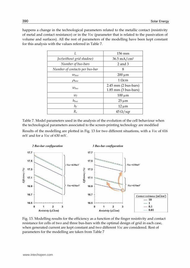
Results of the modelling are plotted in Fig. 13 for two different situations, with a Voc of 616
mV and for a Voc of 630 mV.
Fig. 13. Modelling results for the efficiency as a function of the finger resistivity and contact resistance for cells of two and three bus-bars with the optimal design of grid in each case, when generated current are kept constant and two different Voc are considered. Rest of parameters for the modelling are taken from Table 7
www.intechopen.com
Contact Definition in Industrial Silicon Solar Cells
391
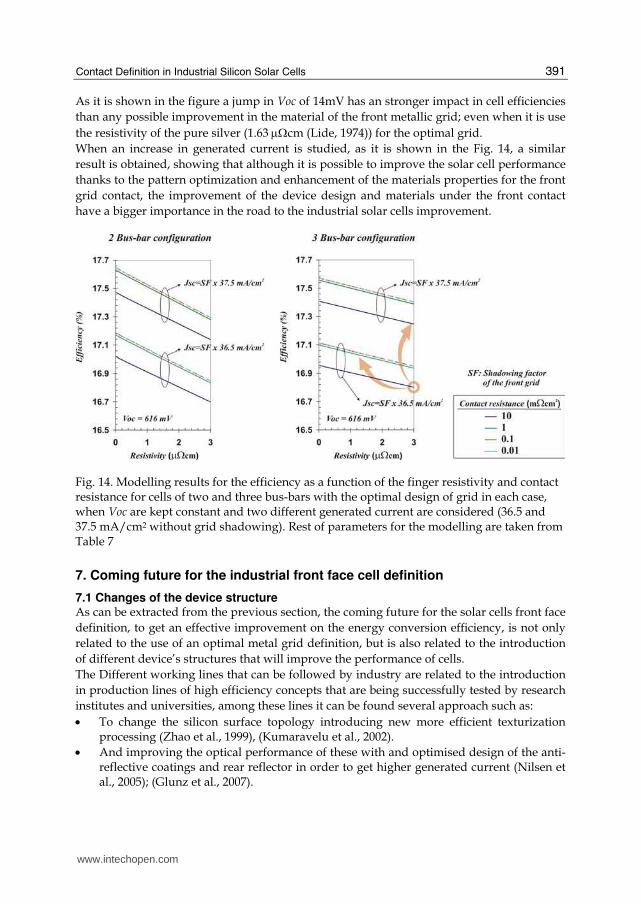
As it is shown in the figure a jump in Voc of 14mV has an stronger impact in cell efficiencies
than any possible improvement in the material of the front metallic grid; even when it is use
the resistivity of the pure silver (1.63 μΩcm (Lide, 1974)) for the optimal grid.
When an increase in generated current is studied, as it is shown in the Fig. 14, a similar
result is obtained, showing that although it is possible to improve the solar cell performance
thanks to the pattern optimization and enhancement of the materials properties for the front
grid contact, the improvement of the device design and materials under the front contact
have a bigger importance in the road to the industrial solar cells improvement.
Fig. 14. Modelling results for the efficiency as a function of the finger resistivity and contact resistance for cells of two and three bus-bars with the optimal design of grid in each case, when Voc are kept constant and two different generated current are considered (36.5 and 37.5 mA/cm2 without grid shadowing). Rest of parameters for the modelling are taken from Table 7
7. Coming future for the industrial front face cell definition
7.1 Changes of the device structure As can be extracted from the previous section, the coming future for the solar cells front face
definition, to get an effective improvement on the energy conversion efficiency, is not only
related to the use of an optimal metal grid definition, but is also related to the introduction
of different device’s structures that will improve the performance of cells.
The Different working lines that can be followed by industry are related to the introduction
in production lines of high efficiency concepts that are being successfully tested by research
institutes and universities, among these lines it can be found several approach such as:
• To change the silicon surface topology introducing new more efficient texturization processing (Zhao et al., 1999), (Kumaravelu et al., 2002).
• And improving the optical performance of these with and optimised design of the anti-reflective coatings and rear reflector in order to get higher generated current (Nilsen et al., 2005); (Glunz et al., 2007).
www.intechopen.com
Solar Energy
392
• Improving the front, bulk and rear surface electrical passivation in order to enhance the final open circuit voltage of the devices, by means of better aluminium rear pastes, using gettering steps or introducing more radical changes in the cell design as a rear local contact with an improved electrical passivation. (Glunz et al., 2007).
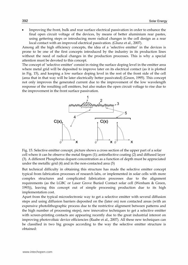
Among all the high efficiency concepts, the idea of a ‘selective emitter’ in the devices is prone to be one of the first concepts introduced by the industry in its production lines without the need of radical changes in the production processes. This is why a special attention must be devoted to this concept. The concept of ‘selective emitter’ consist in rising the surface doping level in the emitter area where metal grid will be deposited to improve later on its electrical contact (as it is plotted in Fig. 15), and keeping a low surface doping level in the rest of the front side of the cell (area that in that way will be later electrically better passivated) (Green, 1995). This concept not only improves the generated current due to the improvement of the low wavelength response of the resulting cell emitters, but also makes the open circuit voltage to rise due to the improvement in the front surface passivation.
Fig. 15. Selective emitter concept, picture shows a cross section of the upper part of a solar cell where it can be observe the metal fingers (1); antireflective coating (2) and diffused layer (3). A different Phosphorus dopant concentration as a function of depth must be appreciated under the metallic grid (4) and in the non-contacted area (5)
But technical difficulty in obtaining this structure has made the selective emitter concept
typical from fabrication processes of research labs, or implemented in solar cells with more
complex structures and complicated fabrication processes due to the alignment
requirements (as the LGBC or Laser Grove Buried Contact solar cell (Wenham & Green,
1993)), leaving this concept out of simple processing production due to its high
implementation cost.
Apart from the typical microelectronic way to get a selective emitter with several diffusion
steps and using diffusion barriers deposited on the (later on) non contacted areas (with an
expensive photolithographic process due to the restrictive alignment between patterns and
the high number of processing steps), new innovative techniques to get a selective emitter
with screen-printing contacts are appearing recently due to the great industrial interest on
improving photovoltaic device efficiencies (Raabe et al., 2007). All these new techniques can
be classified in two big groups according to the way the selective emitter structure is
obtained:
www.intechopen.com
Contact Definition in Industrial Silicon Solar Cells
393
A. Selective emitter developed without masking processes, carrying out local phosphorus diffusion on the wafer surface. Several alternatives for this kind of processes has been studied, among these, it could be emphasized: 1. The local deposition of phosphorus sources on the wafer surface by using a screen-
printing process previous to the high temperature diffusion step, generating most highly doped areas in a self-aligned process that only requires the right location of the contact grid during the metallization step. Different examples of these processes can be found in (Horzel et al., A 1997); (Horzel et al., B 1997); (Salami et al., 2004).
2. The use of lasers to create, after a soft phosphorus diffusion step in all the cell area, a higher doped contact area (Besi-Vetrella et al., 1997).
3. Or the use of special metallization pastes that include doping material in its composition, thereby these pastes are used as a source of dopants for the contact area during the firing step of the metallization, creating a selective emitter structure when they are deposited on wafers with a low doped emitter in a self-aligned fabrication process. Examples of these processes can be found in (Rohatgi et al., 2001); (Porter et al., 2002); (Hilali et al., 2002).
B. Selective emitter developed using masking processes to protect, with barriers, part of the front area from the diffusion step (creating zones with a softer diffusion due to these barriers) (Bultman et al., 2000); (Bultman et al., 2001). Or masking to protect the surface from a selective etching. As it is refer in (Ruby et al., 1997); (Zerga, A. et al., 2006); (Haverkamp et al., 2008).
The alternatives exposed in the first group produce a correct selective emitter structure but have a drawback, after the phosphorus diffusion and the gettering step it introduces, when it is carried out in super-saturation conditions, the impurities concentrations in the silicon bulk keep constant, because impurities remain mainly trapped in the ‘dead layer’ that appears near the surface, without been effectively removed from the device, reducing the potential impact of the improvement this step could have. Among the different alternatives of the second group, however, it exists processes that can carry out an effective reduction of impurities when these include a surface etching, what result in a better device performance; but also present some drawbacks related to the needed mask treatments and processing (such as deposition, curing and removing steps), giving slightly more complex fabrication process. All the developed alternatives in both groups (with exception of the use of self-doped metallization pastes) present a fundamental problem for the selective emitter structure, that is the need of an alignment with the next processing steps for the contact definition, complicating the fabrication routes. This problem gets worse when it is taken into account the random deformation screen-printing technique presents for the transferred patterns with the increase in the number of prints (deformation that is associated to the relaxation of the fabrics, that compose the screens, and gets a maximum value in the mass production environment). But appearance of new alignment relaxed device structures concepts (Caballero, 2009) can help to develop new and easier industrial fabrication processes that could finally result in the implantation of the selective emitter as a common part of the typical industrial solar cell device structures. The introduction of the selective emitter structure would force the re-design of the front contact grid that could present a different optimal finger separation (with closer fingers) due to the increase in the emitter resistance of the new cells, but no other additional important changes.
www.intechopen.com
Solar Energy
394
7.2 The future of the metallic contact definition Apart from the improvement of the general parameters of the device (Voc and Jsc), as
previous sections has shown, improving the front contact of solar cells is possible and it can
produce an increase in the final efficiency of the industrial solar cells. In this section it will
be reviewed the strategies that research centres and industry are following for a future
improvement of the front grid.
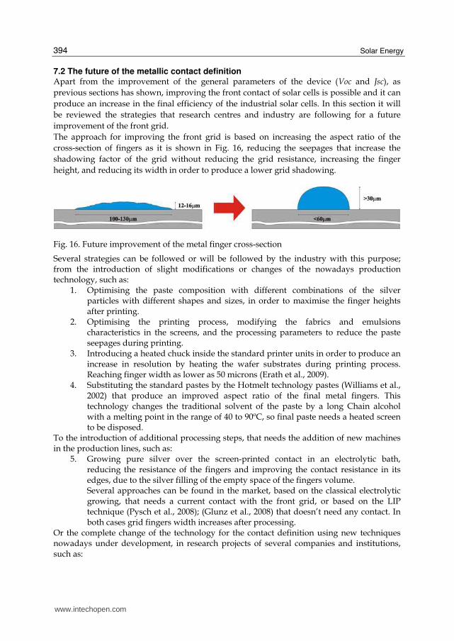
The approach for improving the front grid is based on increasing the aspect ratio of the
cross-section of fingers as it is shown in Fig. 16, reducing the seepages that increase the
shadowing factor of the grid without reducing the grid resistance, increasing the finger
height, and reducing its width in order to produce a lower grid shadowing.
Fig. 16. Future improvement of the metal finger cross-section
Several strategies can be followed or will be followed by the industry with this purpose; from the introduction of slight modifications or changes of the nowadays production technology, such as:
1. Optimising the paste composition with different combinations of the silver particles with different shapes and sizes, in order to maximise the finger heights after printing.
2. Optimising the printing process, modifying the fabrics and emulsions characteristics in the screens, and the processing parameters to reduce the paste seepages during printing.
3. Introducing a heated chuck inside the standard printer units in order to produce an increase in resolution by heating the wafer substrates during printing process. Reaching finger width as lower as 50 microns (Erath et al., 2009).
4. Substituting the standard pastes by the Hotmelt technology pastes (Williams et al., 2002) that produce an improved aspect ratio of the final metal fingers. This technology changes the traditional solvent of the paste by a long Chain alcohol with a melting point in the range of 40 to 90ºC, so final paste needs a heated screen to be disposed.
To the introduction of additional processing steps, that needs the addition of new machines in the production lines, such as:
5. Growing pure silver over the screen-printed contact in an electrolytic bath, reducing the resistance of the fingers and improving the contact resistance in its edges, due to the silver filling of the empty space of the fingers volume. Several approaches can be found in the market, based on the classical electrolytic growing, that needs a current contact with the front grid, or based on the LIP technique (Pysch et al., 2008); (Glunz et al., 2008) that doesn’t need any contact. In both cases grid fingers width increases after processing.
Or the complete change of the technology for the contact definition using new techniques nowadays under development, in research projects of several companies and institutions, such as:
www.intechopen.com
Contact Definition in Industrial Silicon Solar Cells
395
6. Growing the complete finger in an electrolytic processing, but defining previously a grid which is used as a seed for the electrolytic grown with narrow lines to avoid an excessive increase of the final finger width. This seed for growing could be produced with an electroless nickel plating over the bare emitter silicon (Glunz et al., 2008) (processing that would introduce previously, a masking of the front silicon nitride layer using an inkjet printing system to deposit the mask with the needed definition of lines; and an etching of the masked structure to open the nitride layer), or defined with new promising techniques such as inkjet printing (Mills & Branning, 2009), aerosol jet printing (technique able to reach finger definition of 40 microns) (Hörteis et al., 2008), or laser direct-printing (able to reach a finger definition below 20 microns) (Shin et al., 2008); (Arnold et al., 2004) over the silicon nitride layer (with its later firing through previous to the electrolytic growing) or also over the bare silicon emitter (processing that would need also a previously masked etchings of the nitride).
The introduction of the plating of new materials to grow the contact grid can reduce additionally the final cost of the metallization step. Thus, copper with a good conductive properties (97.61% of the silver conductivity (Brady et al., 2002)), is stirring up the industrial interest on the creation of new multiple metal layer contact such as:
Seed of Nickel/ Copper/ Tin Seed of Silver/ Nickel/ Cooper/ Tin or Directly Copper without seed/ Tin
On the other hand, situation for the back aluminium contact of cells is different because it is not related with the improvement of resolution, but with the need of an improvement in Voc to increase the final cell efficiencies. In this case the possible paths for industry to follow are:
• Improving the characteristics of the Aluminium pastes for the total bsf device structure, designing new formulations of the used pastes and removing the limitation that nowadays the aluminium contact has, related with the bowing of devices during the firing process, by means of, for example, adding special thermal treatments processing (Huster, 2005).
• Changing the total rear contact by a local rear contact where non contacted areas must be passivated with a new deposited layer with improved properties of passivation for p type silicon. Laser techniques for the creation of the local contacts (Schneiderlöchner et al., 2002); (Tucci et al., 2008) are taking a good position to be industrialised for the creation of this kind of local contacted structures.
8. Conclusions
This chapter has presented the technique used by the mass production industry to define the contacts of the silicon solar cell, its basic principles and factors that have an influence in its result with the main aim of giving an introductory view of a technique responsible for the development and expansion of the nowadays photovoltaic terrestrial market. It has been shown how through a simple analytical modelling the performance of different designs for the front contact in the commercial solar cells can be optimised and compared. And a quick review of the coming changes in the device structure design, and the future techniques that are under research to substitute the screen-printing technology have been done in order to give an idea of how the industry can evolve in the coming years.
www.intechopen.com
Solar Energy
396
9. References
Arnold, C. B.; Sutto, T. E.; Kim, H.; Piqué, A., ‘Direct-write laser processing creates tiny electrochemical systems’, Laser Focus World, May 2004.
Besi-Vetrella, U. et al., ‘Large area, screen printed Silicon solar cells with selective emitter made by laser overdoping and RTA spin-on glasses’, U. Besi-Vetrella et al., 26th IEEE PVSC, Anaheim, CA, 1997.
Brady, G. S.; Clauser, H. R.; Vaccari, J. A., Materials handbook 15th Edition, Ed. Mc Graw Hill, pg 1106, 2002
Bultman, J. H. et al., ‘Single step selective emitter using diffusion barriers’, Proceedings of the 16th EPVSEC, Glasgow, 2000.
Bultman, J. H. et al., ‘Ideal single diffusion step selective emitters: a comparison between theory and practice’, Proceedings of the 17th EPVSEC, Munich, 2001.
Caballero, F. J., Patent pending concept, ‘Structure of selective emitter in solar cell of easy alignment between patterns for its industrial mass production, with possible local phosphorus gettering process integration and able for in-line processing’, 2009.
Caballero, L.J.; Sánchez-Friera, P.; Lalaguna, B.; Alonso, J.; Vázquez, M.A., ‘Series Resistance Modelling Of Industrial Screen-Printed Monocrystalline Silicon Solar Cells And Modules Including The Effect Of Spot Soldering’, Proceedings of the 4th WCPVSC, Hawaii, 2006.
Erath, D.; Filipovic, A.; Retzlaff, M.; Goetz, A. K.; Clement, F.; Biro, D.; Preu, R., ‘Advanced screen printing technique for high definition front side metallization of crystalline silicon solar cells’, Solar Energy Materials & Solar Cells,V5,Issue 18, 2009.
Firor, K.; Hogan, S., ‘Effects of processing parameters on thick film inks used for solar cell front metallization’, Solar Cells, vol. 5, Dec. 1981, p. 87-100.
Glunz, S. W. et al., ‘High-Efficiency Crystalline Silicon Solar Cells’, Advances in OptoElectronics, Volume 2007, Article ID 97370, Hindawi Publishing Corporation, 2007
Glunz, S. W. et al., ‘Progress in advanced metallization technology at Fraunhofer ISE’, Proceedings of the 33rd IEEE PVSC, San Diego, 2008.
Green , M. A., ‘Silicon solar cells, Advanced principles & Practice’, Centre for photovoltaic devices and systems UNSW, Sydney, 1995.
Haigh, A. D. (Ferranti Ltd.), ‘Developments in Polycrystalline Silicon Solar Cells And A Novel Form Of Printed Contact’. Proceedings of the International Conference on Solar Electricity. France, 1976.
Haverkamp, H. et al., ‘Minimizing the electrical losses on the front side: development of a selective emitter process from a single diffusion’, Proceedings of the 33rd IEEE PVSC, San Diego, CA, 2008.
Hilali, M. et al., ‘Optimization of self-doping Ag Paste Firing to achieve high Fill Factors on
screen-printed Silicon solar cells with 100Ω/sq. Emitter’, Proceedings of the 29th IEEE PVSC, New Orleans, 2002.
Holmes, P. J.; Loasby, R. G., Handbook of Thick Film Technology, Electrochemical Publications Limited, 1976.
Horzel, J. et al., A, ‘Novel method to form selective emitters in one diffusion step without etching or masking’, Proceedings of the 14th EPVSEC, Barcelona, 1997.
Horzel, J. et al., B, ‘A simple processing sequence for selective emitters’, Proceedings of the 26th IEEE PVSC, Anaheim, CA, 1997.
www.intechopen.com
Contact Definition in Industrial Silicon Solar Cells
397
Hörteis, M.; Richter, P. L.; Glunz, S. W., ‘Improved front side metallization by aerosol jet printing of Hotmelt inks’, Proceedings of the 23rd EPVSEC, Valencia, 2008.
Huster,F., Aluminium-Back Surface Field: Bow investigation and Elimination, Proceedings of the 20th EPVSEC, Barcelona, pp. 635-638, 2005.
Kumaravelu, G.; Alkaisi, M. M.; Bittar, A., ‘Surface texturing for silicon solar cells using reactive ion etching technique’, Proceedings of the 29th IEEE Photovoltaic specialists conference, New Orleans, Louisiana, USA, 2002.
Lide, D. R., Handbook of Chemistry and Physics, CRC Press 1974. Luque A. et al. Solar Cells and Optics for Photovoltaic Concentration, chapter 4, Adam Hilger
series on optics and optoelectronics, 1989. Mills, R. N.; Branning, P., ‘Inkjet systems for use in photovoltaic production’, Photovoltaic
World, September 2009. Nilsen , D.; Stensrud, E. and Holt , A., Double layer anti-reflective coating for silicon solar
cells, Proceedings of the 31st IEEE PVSC, Orlando, Florida, USA, pp.1237-1240, 2005.
Porter L. M.. et al., ‘Phosphorus-Doped, Silver-Based Pastes for Self-Doping Ohmic Contacts for Crystalline Silicon Solar Cells’, Sol. Energ. Mat. and Sol. Cells 73 (2), 209-219, 2002.
Pysch, D.; Mette, A.; Filipovic, A.; Glunz, S. W., ‘Comprehensive analysis of advanced solar cell contacts consisting of printed fine-line seed layers thickened by silver plating’, Progress in Photovoltaics, V17, Issue 2, pp. 101-114, 2008.
Raabe, B. et al. ‘Monocrystalline Silicion-Future Cell Concepts’, Proceedings of the 22nd EPVSEC, Milan, 2007.
Ralph, E. L. (Spectrolab Inc.), ‘Recent advancements in low-cost solar cell processing’, Proceedings of the 11th IEEE PVSC, 1975.
Recart, F.,Evaluación de la serigrafía como técnica de metalización para células solares eficientes´,.PhD Thesis, Universidad del Pais Vasco, 2001.
Roberts, S.; Heasman, K. C.; Bruton T. M., ‘The reduction of module power losses by optimisation of the tabbing ribbon’, Proceedings of the 16th EUPVSEC, Glasgow, 2000.
Rohatgi, A. et al., ‘Self-aligned self-doping selective emitter for screen-printed silicon solar cells’, Proceedings of the 17th EPVSEC, Munich, Germany, 2001.
Ruby, D. S. et al., ‘Recent progress on the self-aligned, selective-emitter Silicon solar cell’, Proceedings of the 26th IEEE PVSC, Anaheim, CA, 1997.
Salami, J. et al., ‘Characterization of screen printed phosphorus diffusion paste for Silicon solar cells’, Proceedings of the PVSEC-14, Bangkok, Thailand, 2004.
Shin, H.; Lee, H.; Sung, J. and Lee, M., ‘Parallel laser printing of nanoparticulate silver thin film patterns for electronics’, Appl. Phys. Lett. 92, 233107 (2008).
Schneiderlöchner, E.; Preu, R.; Lüdemann, R.; Glunz, S. W., Laser-fired rear contacts for crystalline silicon solar cells, Progress in Photovoltaics, V. 10 Issue 1, Pages 29 - 34, 2002
Tucci M.; Talgorn, E.; Serenelli L.; Salza, E.; Izzi, M. and Mangiapane, P., ‘Laser fired back contact for silicon solar cells’, Thin Solid Films, Volume 516, Issue 20, pp. 6767-6770, 2008.
Van der Heide A. S. H., Bultman J. H., Hoornstra J., et al. ‘Locating losses due to contact resistance, shunts and recombination by potential mapping with the Corescan’.
www.intechopen.com

Solar Energy
398
Proceedings of the 12th NREL Workshop on Crystalline Silicon Solar Cells, Materials and Processes, Breckenrige (CO), USA, A, 2002
Van der Heide A. S. H., Bultman J. H., Hoornstra J., et al., ‘Optimizing the front side metallization process using corescan’, Proceedings of the 29th IEEE PVSC, New Orleans, USA, B, 2002.
Williams, T.; McVicker, K.; Shaikh, A.; Koval, T.; Shea, S.; Kinsey, B. and Hetzer, D., ‘Hot Melt Ink Technology for Crystalline Silicon Solar Cells’, 29th IEEE PVSC, New Orleans, 2002.
Wenham, S. R. and Green, M.A. Australian Patent 570309, 1993. Zerga, A. et al., ‘Selective emitter formation for large-scale industrially MC-Si solar cells by
hydrogen plasma and wet etching’, Proceedings of the 21st EPVSEC, Dresden, 2006. Zhao, J.; Wang, A.; Campbell, P.; and Green, M. A., ‘A 19.8% Efficient Honeycomb
Multicrystalline Silicon Solar Cell with Improved Light Trapping’, IEEE Transactions On Electron Devices, Vol. 46, No. 10, pp 1978-1983, 1999.
www.intechopen.com
Solar EnergyEdited by Radu D Rugescu
ISBN 978-953-307-052-0Hard cover, 432 pagesPublisher InTechPublished online 01, February, 2010Published in print edition February, 2010
InTech EuropeUniversity Campus STeP Ri Slavka Krautzeka 83/A 51000 Rijeka, Croatia Phone: +385 (51) 770 447 Fax: +385 (51) 686 166www.intechopen.com
InTech ChinaUnit 405, Office Block, Hotel Equatorial Shanghai No.65, Yan An Road (West), Shanghai, 200040, China
Phone: +86-21-62489820 Fax: +86-21-62489821
The present “Solar Energy” science book hopefully opens a series of other first-hand texts in new technologieswith practical impact and subsequent interest. They might include the ecological combustion of fossil fuels,space technology in the benefit of local and remote communities, new trends in the development of secureInternet Communications on an interplanetary scale, new breakthroughs in the propulsion technology andothers. The editors will be pleased to see that the present book is open to debate and they will wait for thereaders’ reaction with great interest. Critics and proposals will be equally welcomed.
How to referenceIn order to correctly reference this scholarly work, feel free to copy and paste the following:
Luis Jaime Caballero (2010). Contact Definition in Industrial Silicon Solar Cells, Solar Energy, Radu D Rugescu(Ed.), ISBN: 978-953-307-052-0, InTech, Available from: http://www.intechopen.com/books/solar-energy/contact-definition-in-industrial-silicon-solar-cells


![Silicon-based solar cells - fotowoltaika.edu.pl. Thin-layer cells and modules ... Silicon -based solar cells – characteristics and production processes ] ] Silicon -based solar cells](https://img.pdfslide.us/doc/110x75/5b0c5ceb7f8b9a6a6b8c3d79/silicon-based-solar-cells-thin-layer-cells-and-modules-silicon-based-solar.jpg)