Embed Size (px)
Citation preview

1
High efficiency silicon and perovskite-silicon solar cells for
electricity generation
Ali Dabirian
Email: [email protected]

From Solar Energy to Electricity
2

Global accumulative PV installed
3In Iran it is about 100 MW.
Total national grid capacity 75 GW.

05.09.2015
Grid-parity in PV is already there
• Swanson PV curve.
4

Photovoltaics Technology
5

Photovoltaics
6
electron
hole
light
V
J
2) In presence of an electric field,
electric charges can be separated
3) The
electricity can
be used !
E scale
Eg
X axis
1) Sunlight is absorbed by a
semiconductor material and its
energy is transferred to an
electron

7
Fundamental limit of efficiency
Single junction ~
In the Schockley-Queisser
radiative limit
(radiative equilibrium of cell
with the sun for a single
semiconductor junction)
33%
Under concentration can be
increased by a few percent !
Radiative Recombination Limit:
W. Shockley and H. J. Queisser, J. Appl. Phys.
32, 510 (1961).Source U. Sydney, only bandgap
Ok, efficiencies might have increased

Major PV technologies
8
Crystalline silicon
Mono and multicrystalline
Status: main market share
Thin films
CIGS, CdTe, Thin film
silicon
Status: stabilised market
share
Emerging technologies
Nano inorganic (Quatum dot)
Organic-Polymer, perovskites
Dye sensitized and variations
Status: niche application
Concentrator technologies
Mostly III-V based
Status: trying entering the
market, many start-ups
Mark
et

PV Technologies market share
9
• Crystalline Si technology does and will hold >90% of PV market share.
• Alternative low-cost technologies have not came close to Si efficiencies and price levels.

Crystalline Si terminology
• Wafer
10
• Cell: processed wafer (20-30 steps)
• Module (a number of cells that are put in series with a two socket as energy output)

Crystalline Si supply chain
11
1.
Solar
grade Si
2.
Ingot
3.
Wafering5.
Module
4.
Cell
processing
On the market:
= 14-21% on monocrystalline Si PV
modules
= 12-18% on multicrystalline Si PV
modules
Features
• Full metal rear side
• Screen printed front
grid
• no local features

Dangling bonds and surface passivation
12
At any semiconductor surface the crystal symmetry is broken
Localized electronic states in the bandgap (whatever the surface condition: bare, in contact with a metallic or oxidized surfaces)
recombination sink for carriers.
Recombination can be avoided by
• Minimizing the number of defects at the surface
• By creating a local electrical field that repels the minority carriers
a) with additional dopants n+ or p-
b) with fixed charges that can create an inversion layer
• By combining the different effects

How does surface passivation work?
13field effect
Inte
rfac
e def
ect
den
sity
bare surface field effect
defect reductionTwo fundamentally different ways
to avoid surface recombination:
1. Repelling of generated carriers
from surface by electrical field
2. Chemical passivation of surface-
states

For good devices:
•Go towards the amorphous-to-crystalline transition as much as possible, but NO
EPITAXY !
Use highly depleted silane plasmas
H2 plasma during a-Si:H growth (‘layer-by-layer’)
5-20 mV gain in Voc
14
Intrinsic films
• Layer properties
Increase in hydrogen content
Increase in band gap
More disordered
Etching effect if H2 plasma is too long
• Globally beneficial for
devices
[Geissbuehler et al., APL 102, 231604 (2013)]

- Measurement of the photoconductivity
- Linked with the carrier density in the wafer
- If bulk is high, surface passivation qualitymay be evaluated.
Surface passivation measurement
cc-Si substratePassivating layershttp://www.sintoninstruments.com
A. Descoeudres et al. IEEE JPV 2013
15

Al-BSF, PERC
16
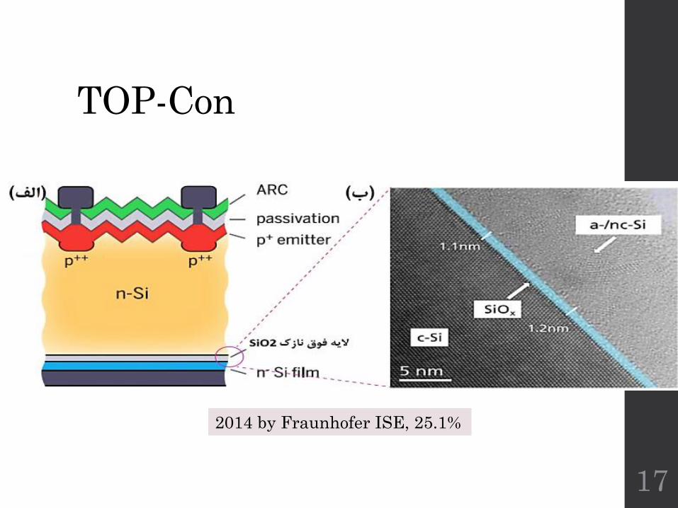
TOP-Con
17
2014 by Fraunhofer ISE, 25.1%

Heterojunction solar cell (Panasonic HIT®)
18
World records:
25.1% (standard):
Keyocera Co.
26.33% (IBC): Kaneka
Co.
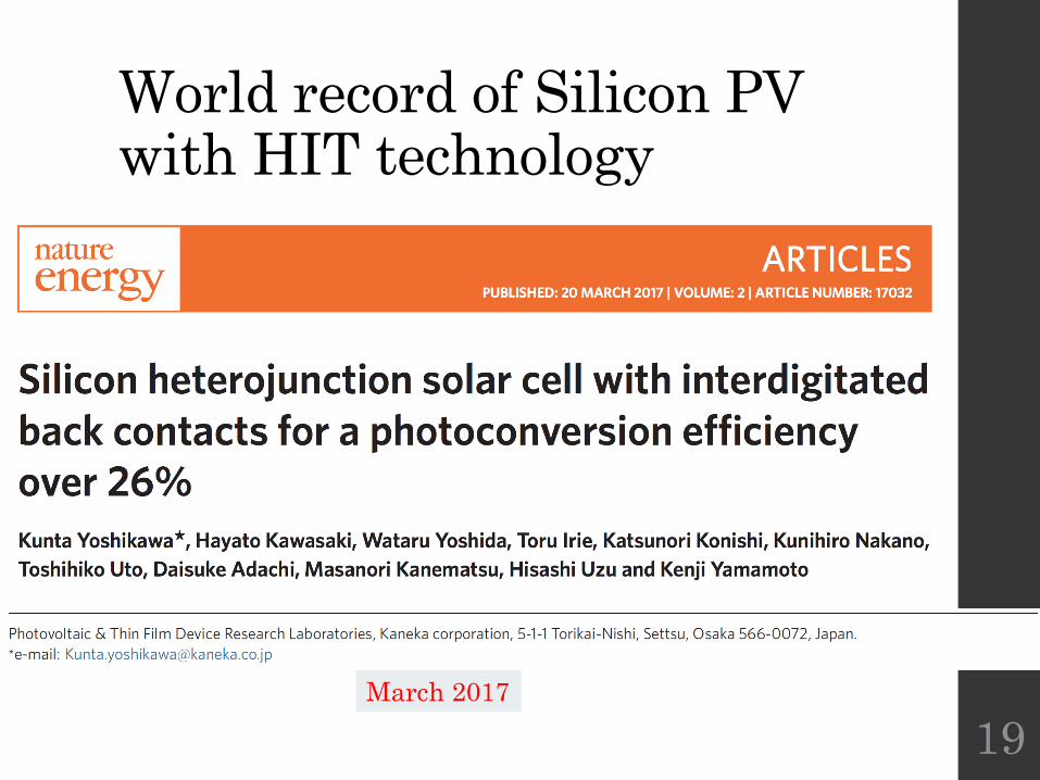
World record of Silicon PV with HIT technology
19March 2017

Efficiences Beyond Si Fundamental Limits
20

Multijunction concept
21

III-V+ Si Tandems
22

Perovskite/c-Si Multi-junction cell
• CH3NH3PbI3 bandgap is 1.56 eV
• c-Si bandgap is 1.1 eV
23

Efficiency beyond 26.33% using perovskite-Si tandem
24P.Loper et al. IEEE JPV., 2015.

Most efficient monolithic perovskite/silicon tandem
25
11.06.2018
Oxford PV reports 25.2 % 156 mm x 156 mm perovskite-silicon tandem solar cells at the company’s industrial pilot line in Brandenburg an der Havel, Germany.(15.06.2018)

Our Research at IPM on Si and Tandem Cells (1. Theory and Simulation)
26A. Dabirian et al. IEEE Journal of Photovoltaics, 7, 718, (2017).
B. Eftekharinia, et al, (in preparation)

2. Our Research at IPM on Si Solar Cell Characterization
27
Solar cell measurement
setups:
1- Temperature variable
IV tester
2- Localized characterization
of solar cells

3. Our Research at IPM on Si PV Modules
28
1- Novel encapsulation
methods2- Colored cells
Glass
Polymer
Polymer
Backsheet
or glass
Solar cell
A. Dabirian et al. patent pending.

4. Our Research at IPM on Fabrication of Tandem Cells
29
Gas-phase deposition of
perovskites for tandems

Acknowledgements
30
Dr. Behrooz Eftekharinia
Hossein Pezeshki
Tahereh Hamedi
Samaneh Eftekhari