Embed Size (px)
Citation preview

2
Epitaxial Silicon Solar Cells
Vasiliki Perraki Department of Electrical and Computer Engineering, University of Patras,
Greece
1. Introduction
Commercial solar cells are made on crystalline silicon wafers typically 300 ┤m thick with a
cost corresponding to a large fraction of their total cost. The potential to produce good
quality layers (of about 50 ┤m thickness), in order to decrease the cost and improve in the
same time the efficiency of cells, has entered to the photovoltaic cell manufacturer priorities.
The wafers thickness has been significantly decreased from 400 ┤m to 200 ┤m, between 1990
and 2006 while the cell’s surface has increased from 100 cm2 to 240 cm2, and the modules
efficiency from 10% to already 13 %, with the highest values above 17% (Photovoltaic
Technology Platform; 2007). Advanced technology’s solar cells have been fabricated on
wafers of 140 ┤m thicknesses, resulting to efficiencies higher than 20% (Mason.N et al 2006).
The cost associated to the substrate of a crystalline silicon solar cell represents about 50-55%
on module level and is equally shared between the cost of base material, crystallization and
sawing (Peter. K; et al 2008). The cost related to the Si base material can be reduced
fabricating thinner cells, while the cost of crystallization and sawing is eliminated by
depositing the Si directly on a low cost substrate, like metallurgical grade Si. The epitaxial
thin- film solar cells represent an attractive alternative, among the different silicon thin film
systems, with a broad thickness range of 1-100┤m (Duerinckh. F; et al 2005). Conversion
efficiencies of 11.5-12 % have been achieved from epitaxial solar cells grown on Upgraded
Metallurgical Grade Silicon (UMG Si) substrates with an active layer of 30 ┤m, and an
efficient BSF (Hoeymissenet. J.V; al 2008). Epitaxial cells with the same active layers
deposited on highly doped multi-crystalline Si substrates by Chemical Vapor Deposition
and the front and back surfaces prepared by phosphorous diffusion as well as screen
printing technique, have confirmed also efficiencies 12.3% (Nieuwenhuysen. K.V; 2006).
Solar cells developed by a specific process for low cost substrates of UMG silicon have led
to efficiencies of 12.8% (Sanchez-Friera. P; et al 2006). Better results have been achieved from
cells with an emitter epitaxially grown by CVD, onto a base epitaxialy grown
(Nieuwenhuysen. K.V; et al 2008). The emitter creates a front surface field which leads to
high open-circuit voltages (Voc) resulting to cell efficiencies close to 15% by optimizing the
doping profile and thickness of epitaxial layers and by including a light trapping
mechanism.
This chapter first describes the manufacturing procedures of epitaxial silicon solar cells, starting from the construction of the base layer until the development of solar cells. Then a one- dimensional (1D) (Perraki.V; 2010) and a three dimensional (3D) computer program (Kotsovos. K & Perraki.V; 2005), are presented, for the study of the n+pp+ type
www.intechopen.com

Solar Cells – Silicon Wafer-Based Technologies
30
epitaxial solar cells. These cells have been built on impure (low cost) polycrystalline p+ silicon substrates (Upgraded metallurgical grade UMG-Si), by a special step of thin pure Si deposition followed by conventional techniques to build a n+/p junction, contacts and antireflective coating (ARC). The software developed expresses the variations of photovoltaic parameters as a function of epilayer thickness and calculates for different values of structure parameters, the optimised cell’s photovoltaic properties. According to the one dimensional (1D) model, the photocurrent density and efficiency are calculated as a function of epilayer thickness in cases of low and high recombination velocity values, as well as in cases of different doping concentration values (Perraki.V; 2010), and their optimum values are figured. The parameter chosen for the cell's optimisation is the epitaxial layer thickness, through variation of grain size and grain boundary recombination velocity, according to the three dimensional (3D) model (Kotsovos. K, & Perraki. V, 2005). Furthermore, a comparison among simulated 3D, 1D and corresponding experimental spectral response results under AM 1.5 illuminations, is presented.
2. Epitaxial silicon solar cell fabrication
The manufacturing sequence for epitaxial silicon (Si) solar cell can be divided in the following main steps: base/active layer formation, junction formation, antireflective coating (ARC) and metallization (front and back contacts), including the oxidation technology, and auxiliary technologies. A complete flow diagram for the realisation of n+pp+ type epitaxial solar cells is presented in Table 1.
MG-Si → UMG-Si→ HEM process p+ type Si → CVD epitaxy→pp+→ Junction formation ...n+pp+ type solar cell ←Back contact formation ←Front grid structuring ←ARC← n+pp+
Table 1. Epitaxial solar cell’s process
2.1 Base layer
The active layer of n+pp+ type crystalline Si solar cells is a thick layer doped with boron and is thus p-type layer with concentration of 1017 cm-3. The crystalline silicon photovoltaic technology has focused on reducing the specific consumption of the base material and increasing the efficiency of cells and modules and in the same time on using new and integrated concepts. Many research groups have tried to use very thin bases in silicon solar cells, aiming to decrease their cost. One of the possible ways for the achievement of cheap crystalline silicon solar cells on an industrial basis is the “metallurgical route”. The different steps of this route are: Metallurgical grade (MG), silicon powder (raw material) is upgraded by water washing, acid etching and melting, resulting to a material with insignificant properties and a measured value of diffusion length, Ln, smaller than 5 ┤m. The Upgraded Metallurgical Grade (UMG), silicon is further purified and recrystallized into ingots by the Heat Exchange Method (HEM) so that to give crack-free ingots associated with large metal impurity segregation and cm size crystals, with better but still insignificant properties. This is due to the fact that the HEM technology allows removing metallic impurities, but the high concentration of boron, phosphorus and the presence of Si carbide precipitates are responsible for again very low measured values of Ln, and solar cell
www.intechopen.com

Epitaxial Silicon Solar Cells
31
efficiencies. In order to overcome the problem this material is used as a cheap p+ -type substrate, on which a thin p-type epitaxial layer is formatted. Epitaxial layer from pure Si is deposited, by chemical vapor deposition (CVD) on these impure UMG polycrystalline substrates, in an epitaxial reactor (Caymax.M, et al 1986). The wafers are first acid etched and cleaned at 1150 0C, then coated with silicon under SiH2Cl2 flow in H2 gas at 1120 0C with a growth rate 1┤m. min-1 (table 2). B2H6 is used, so that to get p- type layers. When the process has been completed a control is carried out testing the quality, thickness and dopant concentration. On to this layer the n+/p junction is then built and epitaxial solar cells are realized, using a low cost screen printing technology.
Remove saw damage by etching
Wafer cleaning
HCl etching in epitaxial reactor
Deposition of the epitaxial layer
Table 2. Flow diagram of the CVD epitaxial process
The technology of Liquid Phase Epitaxy (LPE) has recently applied on metallurgical grade Si with interesting results as well (Peter.K et al 2002).
2.2 Junction formation
Two different approaches exist for the manufacture of the n+-p junction: the ion implantation and the diffusion from the solid phase or from the vapor phase (Overstraeten. R. J. V & Mertens. R, 1986). a. The ion implantation is characterized by excellent control of the impurity profile, low
temperature processing, higher conversion efficiencies, and is rather used in the manufacture of spatial solar cells, due to the high costs associated with it.
b. The diffusion process, from both gaseous and liquid phase, is usually applied for silicon solar cell fabrication. N2, Ar and O2 are used as carrier gases, with quantities and mixing proportions as well as temperature, time and dopant concentration on the surface under, a very accurate control.
Diffusion from the vapor phase consists of diffusion of phosphorus from the oxide formed onto the silicon surface when N2 carrier gas and POCl3 are used in a heated open-tube furnace process at 800-900 0C. Disadvantages of the method are that, diffusion appears on both sides resulting to a back parasitic junction which has to be removed and non uniformity in cases of very shallow junctions. Diffusion from a solid phase consists of deposition of a dopant layer at ambient temperature
followed by a heat treatment, in an electrically heated tube furnace with a quartz tube, at a
temperature ranging from 800 to 900 0C. This process can be performed using chemical
vapor deposition (CVD), screen printing technique, spin-on or spray-on, forming thus only a
junction on the front surface.
i. The CVD technique concerns the deposition, at low temperature, of a uniform phosphorus oxide on the wafer’s front surface. This technique uses, highly pure, expensive, gases ensuring a uniform profile and defined surface conditions.
www.intechopen.com

Solar Cells – Silicon Wafer-Based Technologies
32
ii. Screen printing is involved to thick film technologies which are characterized by low
cost production, automation and reliability. In a first step, a paste rich in phosphorus is
screen printed onto the silicon substrate. Then, phosphorus is diffused throughout a
heat treatment in an open furnace, under typical peak temperatures between 900 and
950 0C, to form the n-p junction.
iii. Spin-on and spray-on of doped layers yield to high throughput but non uniform surfaces.
2.2.1 Diffusion theory
As the diffusion procedure, is usually applied for silicon solar cell fabrication, it is necessary
to refer in brief the theory of diffusion, of various solid elements in the Si solid. This process
obeys to Fick’s second law, which is expressed in one dimension by the following partial
differential equation (Carslaw. H.S; and Jaeger .J.C 1959), (Goetzberger.A, et al 1998).
2
2
( , ) ( , )N t N tD
t
(1)
Where N ( , t) stands for the concentration of the diffusing elements at point and time t
and D the diffusion coefficient, characteristic of each material. This coefficient strongly depends on temperature according to the following relation (Sze. S. M. 1981).
0 exp( / )D D kT (2)
D0 and ⦆〝 (activation energy) are constant for a given element over wide temperature and concentration ranges. The temperature plays a very important role in the diffusion process due to the temperature
exponential dependency of diffusion coefficient. The diffusion coefficients in relation to
temperature show that metals like Ti, Ag, Au, have higher diffusion coefficients D by
several orders of magnitude compared to dopants As, P, B, and consequently they diffuse
faster in Si, while elements such us Cu, Fe diffuse even more quickly. Therefore solar cell
technology requires excellent cleanness of laboratory and experimental devices. However
diffusion time does not affect so much the depth of penetration as this is proportional to its
root square.
Two solutions to the partial differential equation 1 are considered. In the first case the
dopant source is inexhaustible, the surface doping concentration Ns is considered constant
during the diffusion process and the bulk concentration depends on diffusion time and
diffusion temperature. The mathematical solution under boundary conditions concerning
the parameters Ns, t, Nx, and reads:
( , )2
SN t N erfcDt
(3)
Where, erfc stands for the complementary error function distribution.
In order to calculate the depth j of the n-p junction, it is necessary to express the ratio of
bulk concentration in the base silicon to surface concentration (N t /NS) as a function of
/ Dt and choose diffusion constant, temperature, and time.
www.intechopen.com

Epitaxial Silicon Solar Cells
33
In the second case, during the diffusion process there is an exhaustible dopant source on the
surface with a concentration Q (cm-2). The solution of the differential equation 1 N( ,t)
(Gaussian distribution) at point and time t is given by Eq 4:
2( , ) exp ( )2
QN t
Dt Dt
(4)
The surface concentration in this case is expressed as a function of the diffusion parameters by Eq 5:
S
QN
Dt (5)
The penetration depth j of the n-p junction is again calculated by the ratio of the
concentration in the base silicon to surface concentration (N t /NS) when diffusion constant,
temperature and time are also determined.
2.2.2 Emitter’s diffusion procedure
The silicon base wafers are etched, to remove damage from the wafering process (or to prepare after the CVD process) and cleaned, in order to introduce dopant impurities into the base in a controlled manner and form the n-p junction. Since the starting wafers for solar cells are p-type, phosphorus is the n- type impurity
generally used. The n+-doped emitter of the cell is thus created by the diffusion of phosphorus,
in high concentration which is introduced in the form of phosphine (PH) or gaseous
oxychloride (POCL3) into the diffusion furnace. The later is introduced using nitrogen N2, as a
carrier gas. The disadvantages of this method are the formation of a back parasitic junction as
the diffusion occurs on both sides and a non uniformity for very shallow junctions.
At the high temperatures of approximately 800 0C the dopant gases react with the surface of the silicon when oxygen is added, in accordance with the chemical reaction
Si+O2 →SiO2
Silicon dioxide (SiO2) is produced on the surface and secondly, phosphine is converted to
phosphorus pentoxide (P2O5 ) according to the following chemical reaction
2PH+3O2 → P2O5+H2O
The P2O5 created combines with the SiO2 which is grown on the silicon surface to form
liquid phosphorus silicate glass which becomes the diffusion source.
Phosphorus diffusion (at temperatures of 950 0C) as a function of diffusion time shows deviating behaviour from the theory for the case of low penetration depth. This behaviour has been explained by several authors; however it has the disadvantage for solar cells that a dead layer is created, of about 0.3 ┤m thickness, which reduces efficiency to approximately 10%. According to an advanced process, a dead layer can be impeded using a double diffusion process (Blacker. A. W, et al 1989). The first diffusion step consists of a predisposition coat with a low level diffusion of phosphorus at a temperature of approximately 800 0C. Then the phosphorus silicate glass layer is removed by chemical means and in a second diffusion step, this time at a temperature 1000-1100 0C, the desired
www.intechopen.com

Solar Cells – Silicon Wafer-Based Technologies
34
penetration depth of phosphorus is achieved. Surface concentrations of approximately 1019 cm-3 can be obtained.
2.2.3 Screen printing for junction formation
A process line based on the use of thick film technology offers advantages of low cost, automation, and reliability. The technology involves the screen printing technique for the junction formation. According to this a phosphorus-doped paste, containing active material, solvents and a thickener is printed through screens, onto a silicon substrate (Overstraeten. R. J 1986). After printing, the substrate is dried at 150 0C allowing thus the solvents to evaporate. The phosphorus diffuses from the printed layer into the silicon during a heat treatment in a belt furnace in nitrogen under typical peak temperatures between 900 and 950 0C. When screen printing is used for junction formation there is no parasitic junction formed at the back as in the case for open tube diffusion. However the layer that remains on the front of the cell after diffusion and the edges of the substrate which are doped due to contamination, have to be removed by etching in a proper chemical solution followed by a cleaning step. Apart from the junction formation screen printing process can also be applied to the antireflection coating formation and the metallization (front and back contacts). Epitaxialy growth by CVD may also be used for the n+ doped emitter formation, controlling the doping profile, on an epitaxially grown base. In this way a front surface field (FSF) is created yielding to a high open circuit voltage (Voc) and high efficiency (Nieuwenhuysen. K.V; et al 2008).
2.3 Antireflection processes 2.3.1 Antireflection Coating (ARC)
Silicon surfaces reflect more than 33% of sunlight depending upon wavelength. For the manufacture of antireflection coatings industrial inks which contain titanium dioxide (TiO2) or tantanium pentoxide (Ta2O5) as the active coating material, are used. Two technologies are applied for this purpose: a. High vacuum evaporation technologies use almost exclusively TiO2, with a refraction
index n adjusted between 1.9 and 2.3, a good transparency which favors high efficiencies and high costs.
b. Thick film technologies, which are used in mass production due to their lower cost. At thick film technologies, a paste containing TiO2 compounds is deposited onto the surface of silicon, either by the screen printing technique at temperatures of 600 to 800 0C or by the spinning on technique.
The antireflective coating and the front side grid formation can be combined and made together by screen printing technique. In this case the TiO2 paste is firstly dried at temperatures around 200 0C, then a silver paste is added to it for the grid formation, and both are simultaneously sintered. A further improvement can reduce total reflection to 3 – 4%. This can be achieved by using two antireflection layers, with a refractive index decreasing from the upper AR layer to the lower.
2.3.2 Textured surfaces
The textured surfaces of cells allow most of the light to be absorbed in the cell, after multiple reflections. For the construction of textured silicon surfaces the physical-chemical effect is
www.intechopen.com

Epitaxial Silicon Solar Cells
35
used, that the etching rate of silicon in an alkaline solution depends on the crystallographic orientation of silicon’s front surface (Price J.B., 1983). The crystal orientation yielding to high efficiency solar cells is <100>. The anisotropic etching process takes place in weak solutions of KOH or NaOH with a
concentration of 10% up to 30% at approximately 70 0C. This configuration results to
inverted pyramid structures, under well determined conditions and reduces the reflection of
sunlight to approximately 10 % (Goetzberger.A, et al 1998).
An additional ARC allows a further reduction to approximately 3%. In practice the best
success has been achieved with inverted pyramids.
2.4 Contacts 2.4.1 The structuring of the finger grid
The technologies used for the structuring of the finger grid are three: a. The vacuum evaporation, which has the disadvantage that the smallest finger width is
approximately 100 ┤m or at best 50 ┤m, b. The photoresist technique which is used if narrower contact fingers are required in
order to reduce shadowing. c. The screen printing technique, which uses metal pastes, and dominates in a wide range
of production techniques as it is particularly cost effective, with the maximum finger width about 100 ┤m.
This technique is widespread in industrial solar cell manufacturing and has automating processes (Overstraeten. R.J.V; 1986). The screen printing process uses metal pastes containing in addition to 70% Ag approximately 2% sintered glass. After depositing, the layer is sintered at temperatures of about 600 0C, while the sintered glass components melt and dissolve a small layer of silicon. At the same time this melt is enriched by silver. Upon cooling a recrystallized Si layer is created as with normal alloying, which contains a high proportion of Ag and thus creates a good ohmic contact. This process gives quite low contact resistances on the n+ emitter at surface concentrations of approximately 1020 cm-3.
2.4.2 Back surface contacts
The realizations of back surface contacts need only aluminum, in the form of paste. This element has the advantage that forms alloys at its eutectic point 577 0C, and has a good solubility with concentrations of about 1019 cm-3 in Si, while a silver palladium paste is often sintered onto this layer in different cases (Overstraeten. R. J. V, & Mertens. R, 1986). Thus a high doping p+ type is achieved in the recrystallised layer providing a Back Surface Field. Normally sintering takes place at temperatures around 800 0C with the best results. A
significant increase in Voc is observed yielding thus higher values of solar cell efficiency.
2.5 Oxidation technologies
The oxidation technology is applied for the manufacture of a SiO2 layer in solar cells. It is a relatively simple manufacturing process using high temperature treatment in an electrically heated tube furnace with a quartz tube under oxygen. This layer, nevertheless, plays a crucial role in silicon solar cells, with main characteristics passivation and masking effects of SiO2 regarding impurities, which contributes positively to making silicon the basic material for most semiconductor devices.
www.intechopen.com

Solar Cells – Silicon Wafer-Based Technologies
36
Dry oxidation is achieved when silicon is heated without the addition of water vapour, and takes place according to the chemical reaction
Si+ O2→ SiO2
As it is known, oxygen diffuses through the SiO2 layer which is formed, there is no saturation thickness and the layer thickness grows in proportion to time or in proportion to the square root of time at greater layer thickness than 1 ┤m. Wet oxidation, is achieved when silicon is exposed to water vapor, during the oxidation process and obeys to the following chemical reaction
2Si+ O2+2H20 → 2SiO2+2H2
Due to the hydrogen presence in case of wet oxidation the rate of growth is significantly higher than that of dry oxidation (Wolf H. F., 1976). Other influences that also alter the growth rate of SiO2 are the doping concentration of silicon, the orientation of Si surfaces and the addition of chlorine ions during the oxidation process. The use of SiO2 as a passivating layer in solar cells has shown that dry oxidation under high oxidation temperatures yields very low surface recombination rates, which can be reduced even further by an annealing process at about 4500 C, and depends upon the crystallographic orientation of silicon surfaces. The masking effect of a SiO2 layer in the diffusion process relies upon the fact that the diffusion rate of many diffusants in silicon dioxide is lower by orders of magnitude than in silicon itself. The required SiO2 layer thickness, for different diffusion temperatures and times, shows that boron is masked by significantly thinner SiO2 layers than is phosphorus. Furthermore, SiO2 is used for masking in alkaline etching processes as well as for surface texturing (Goetzberger.A, et al 1998).
2.6 Back Surface Field (BSF)
The required p+ doping in the starting wafer, in order to create a Back Surface Field, (BSF), is achieved by diffusion of boron. BBr3 serves as the boron source for this purpose, which can be handled in a very similar manner to POCl3. As it is known, a BSF is necessary for high efficiency solar cells. In industrial practice, aluminium with a eutectic point 577 0C, is introduced onto the surface for the creation of a BSF. This is processed by vacuum evaporation or by screen printing technique at approximately 800 0C.
2.7 Auxiliary technologies
Auxiliary processes such as etching and cleaning are necessary for the manufacture of solar cells. Etching and cleaning techniques are used in order to make the surfaces of silicon wafers free of contaminants like molecular (residues of the lapping, polishing etc), ionic (from the etching solutions), or atomic (heavy metals). The most widely used procedure for surface cleaning is currently the RCA cleaning (named after the company RCA). This process is based upon the use of hydrogen peroxide (H2O2) firstly as an addition to a weak solution of ammonium hydroxide (NH4OH) and secondly hydrochloric acid (HCl). Etching of silicon dioxide layers occurs mainly in a weak solution of hydrofluoric acid, or in combination with ammonium fluoride (NH4F).
www.intechopen.com

Epitaxial Silicon Solar Cells
37
Isotropic etching of silicon occurs in a solution of nitric acid and hydrofluoric acid or in combination with acetic acid and phosphoric acid (H3PO4). Rinsing with deionised water must take place as the final stage, following all cleaning processes. With this processes, specific resistance values near to the theoretical value are achieved.
3. Mathematical model
A one dimensional (1D) analytical model is assessed via a simulation program which takes into account the interaction and the limitations between several parameters. By modeling short circuit current density Jsc, open circuit voltage Voc and efficiency η, cells of different structure characteristics are studied. The photocurrent density and efficiency are estimated as a function of epilayer thickness d2, for various values of recombination velocity and doping concentration (Perraki V, 2010). Furthermore, the simulated and experimental plots of quantum efficiency are compared, under 1000W/m2 irradiation. A three dimensional (3D) analytical model, which is based on the Green's Function method, is also implemented at the same cells. The model is applied via a simulation program to optimize the efficiency of cells. The parameter chosen for optimization is the epitaxial layer thickness via variation of grain size and grain boundary recombination velocity (Kotsovos K, & Perraki V., 2005). In addition, 3D spectral response data are compared with the 1D results.
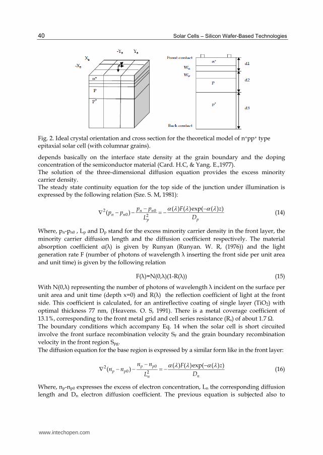
3.1 One dimensional model
The epitaxial n+pp+ type Si solar cell is divided in four main regions (front layer n+, Space Charge Region (SCR), epilayer, and substrate), with thickness d1-wn, wn+wp, d2-wp and d3, respectively, figure 1.
Fig. 1. The cross section for the theoretical model of n+pp+ type epitaxial solar cell.
There are a number of main assumptions used for modeling which concern, the homogeneity of physical and electrical properties of the grains (doping concentration, minority carrier mobility, life time and diffusion length). The grains are columnar, in Si materials recrystallized by the Heat Exchange Method, becoming increasingly large when considering successively, bottom, middle and top wafers in the ingot. These columnar grains are perpendicular to the front and to the n+/p junction. The front surface recombination velocity SF has a value of 104 cm/s and the back surface SB 1015
cm/s. A perfect abrupt interface between the heavily doped substrate with thickness higher
www.intechopen.com

Solar Cells – Silicon Wafer-Based Technologies
38
compared to its diffusion length and the lowly doped epilayer, consists a low/high junction
p/p+. This junction produces a strong BSF while the p+ layer does not contribute to the total
photocurrent (Luque. A, & Hegeduw. S., 2003).
The expression, for the effective recombination velocity, Seff, at the epilayer/substrate
interface describing the quality of the back surface of the base, is given by the following
equation (Godlewski. M; et al 1973):
3 3
3 3
( cosh sinh )
(cosh sinh )
B n
A n n n neff
B nA n
n n n
S L d d
N D D L LS
S LN L d d
L D L
(6)
Where, the terms ΝΑ, ΝΑ+,Ln, Ln+, Dn, Dn+ stand for the material’s doping concentration,
electron diffusion length and diffusion constant in the epilayer and the substrate
respectively and SB for the recombination velocity at the back surface. Due to the low/ high
junction the following simplified relation (Arora. J, et al 1981) gives the expression for Seff.
A n
eff
A n
N DS
N L
(7)
The terms NA, NA+, Dn+ and Ln+ are assumed constant all over of these regions’ bulk.
The analytical form of the quantum efficiency of the front layer Qp, is described by the
following relation (Hovel H J 1975), (Sze. S. M, 1981):
1 11
21 1
( ) [ cosh sinh ]exp( )
[1 ] [( ) 1 sinh cosh
n nF P F Pn P n n n
n P P P P PP
n nF Pn P
P P P
d w d wS L S LL d a w
L D D L LQ R x
d w d wS LLD L L
1exp( )]n p n n nL d w (8)
Where Lp, Dp and αn stand for hole diffusion length, diffusion coefficient and absorption
coefficient in the front layer and R and SF stand for reflection coefficient and front surface
recombination velocity, respectively.
The base region quantum yield Qn, can be calculated from the following relation
12[1 ] exp( ( ))
( ) 1P n
n n p pP n
LQ R d W
L
2 22
2 2
sinh cosh ( )exp ( )
[ ]
sinh cosh
p eff n p eff nP n p p
n n n nP n
eff n p p
n n n
d w S L d w S LL d w
L D L DL
S L d w d w
D L L
(9)
αp stands for the absorption coefficient in the base layer p.
www.intechopen.com

Epitaxial Silicon Solar Cells
39
The contribution of the space charge region QSCR is expressed by the following relation (Sze .S.M 1981)
QSCR=[1-R][exp-(αnWn+αpWp)-1]exp-αn(d1-Wn) (10)
The contribution of the three regions of the solar cell is:
Qtot=Qp+Qn+QSCR (11)
The total photocurrent density Jsc arising from the minority carriers generated very near the junction in the n- layer, in the epilayer and in the space charge region can be calculated from the Eq. 12 as a function of the cell’s quantum efficiency.
1.1
0.4
( ) ( )SC totJ q Q N d (12)
The flux of photons as a function of wavelength, Ν (┣), was defined by a discretized AM1.5 solar spectrum. The open circuit voltage depends on the Boltzmann constant, k, the solar cell operating temperate, T, the elementary electron charge, q, and the logarithm of the ratio between the photocurrent and dark current density, Jsc /J0.
0
ln( 1)SCOC
JkTV
q J (13)
Moreover, efficiency η (%) which is the most important parameter in the evaluation process of photovoltaic cells, is proportional to the open-circuit voltage Voc, the photocurrent density Jsc, fill factor FF, and inversely proportional to the incident power of sunlight.
3.2 Three dimensional model (3D)
Several assessments have been admitted in order to simplify the 3D model and obtain the
excess minority carrier density from the solution of the three-dimensional diffusion equation
in each region.
The p/p+ junction is considered as a low/high junction, incorporating a strong BSF. It is
assumed that the p+ region’s contribution to the total photocurrent is negligible (Dugas.J, &
Qualid. J, 1985).
The heat exchange method provides polycrystalline silicon with columnar grains, as shown
in figure 2. The grain boundaries are surfaces of very small width compared to the grain
size, characterized by a distribution of interface states. They are perpendicular to the n+/p
junction, becoming increasingly large when considering successively, bottom, middle and
top wafers in the ingot. Their physical and electrical properties, concerning the doping
concentration, the mobility and diffusion length of minority carriers, along the three
dimensions are homogeneous, for each region. There are ignored effects of other
imperfections of the crystal structure.
The front and back surface recombination velocity SF and SB are the same as in (Luque. A, & Hegeduw. S., 2003), and their values are assumed as 104 cm/sec and 1015 cm/sec respectively. The effective grain boundary recombination velocity is assumed constant all over the surface of the grain and has been estimated to vary from 102 to 106 cm/sec. It
www.intechopen.com
Solar Cells – Silicon Wafer-Based Technologies
40
Fig. 2. Ideal crystal orientation and cross section for the theoretical model of n+pp+ type epitaxial solar cell (with columnar grains).
depends basically on the interface state density at the grain boundary and the doping concentration of the semiconductor material (Card. H.C, & Yang. E.,1977). The solution of the three-dimensional diffusion equation provides the excess minority carrier density. The steady state continuity equation for the top side of the junction under illumination is expressed by the following relation (Sze. S. M, 1981):
2 00 2
( ) ( )exp( ( ) )( ) n n
n npp
p p F zp p
DL
(14)
Where, pn-pn0 , Lp and Dp stand for the excess minority carrier density in the front layer, the
minority carrier diffusion length and the diffusion coefficient respectively. The material
absorption coefficient α(┣) is given by Runyan (Runyan. W. R, (1976)) and the light
generation rate F (number of photons of wavelength ┣ inserting the front side per unit area
and unit time) is given by the following relation
F(┣)=N(0,┣)(1-R(┣)) (15)
With N(0,┣) representing the number of photons of wavelength ┣ incident on the surface per
unit area and unit time (depth x=0) and R(┣) the reflection coefficient of light at the front
side. This coefficient is calculated, for an antireflective coating of single layer (TiO2) with
optimal thickness 77 nm, (Heavens. O. S, 1991). There is a metal coverage coefficient of
13.1%, corresponding to the front metal grid and cell series resistance (Rs) of about 1.7 Ω.
The boundary conditions which accompany Eq. 14 when the solar cell is short circuited
involve the front surface recombination velocity SF and the grain boundary recombination
velocity in the front region Spg.
The diffusion equation for the base region is expressed by a similar form like in the front layer:
02
0 2
( ) ( )exp( ( ) )( )
p pp p
nn
n n F zn n
DL
(16)
Where, np-np0 expresses the excess of electron concentration, Ln the corresponding diffusion length and Dn electron diffusion coefficient. The previous equation is subjected also to
www.intechopen.com

Epitaxial Silicon Solar Cells
41
specific boundary conditions when the device is operated under short circuit, concerning the grain boundary recombination velocity in the active layer Sng and the effective back surface recombination velocity Seff at the low / high junction. The simplified relation gives the expression for effective electron recombination velocity Seff, as a function of the material’s doping concentration of the active layer and the substrate (ΝΑ, ΝΑ+), assumed constant all over of these regions’ bulk (Eq.7). Moreover the grain boundary recombination velocity in the front and the active layer is considered the same and symbolized as Sgb. The solution of the continuity equations (14) and (16) is obtained in analytical form using the
Green’s function method. This procedure is briefly described in (kotsovos. K & Perraki. V;
2005). The analytical expression of the front layer photocurrent density Jp is derived, by
differentiating the hole density distribution in the junction edge region z=d1-wn presented in
the form of infinite series (Halder. N.C, & Williams. T. R., 1983):
2 2
2 2,
( , , ) 4
sin( )sin( )cos( )cos( )
( 1)
p
peff x y g g
m n peff
J x y q F
L M N mX nYmx ny
mn L
1 11
11 1
exp( ( )){ cosh( ) sinh( )}
[ exp( ( ))]
sinh( ) cosh( )
n np peff n p
peff peffpeff n
n np
peff peff
d w d wN L d w N
L LL d w
d w d wN
L L
(17)
where the variables x and y represent arbitrary points inside the grain and Mx, Ny, Lpeff, Np
are expressed by proper equations as functions of Spg ,Dp, Xg, Yg, Lp, and SF.
In a similar way the analytical expression of the base region photocurrent density Jn is given,
in the form of infinite series, by differentiating the electron density distribution in the
junction edge region z=d2 –wp by the relation
1( )
2 2
2 2,
4
sin( )sin( )cos( )cos( )
( 1)
pd wn
neff x y g g
k l neff
J q Fe
L K L kX lYkx ly
kl L
2 2( ) ( )2 2
2 2
{cosh( ) ) sinh( )} )
[ ]
sinh( ) cosh( )
p pd w d wp pn neff
neff neffneff
p pn
neff neff
d w d wN e L e
L LL
d w d wN
L L
(18)
Where Kx, Ly, Lneff, Nn are expressed as functions of Seff, Sng ,Dn, Xg, Yg, Ln.
The photogenerated current in the Space Charge Region (equal to the number of photons
absorbed), is derived by the 1D model (Sze. S. M, 1981):
1( )( ){1 }n pnw wd w
SCRJ qFe e (19)
www.intechopen.com

Solar Cells – Silicon Wafer-Based Technologies
42
The total photocurrent is given from the sum of all current densities in each region considering as it has been early referred (Dugas. J.& Qualid. J, 1985) that the substrate contribution is negligible:
sc p n SCRJ J J J (20)
A similar analysis might also carried out, for the determination of the dark saturation current (J0) by solving the continuity equations, for both regions, (Halder. N. C, & Williams. T. R., 1983). The derived expression of J0 is then used for the calculation of open circuit voltage from Eq 13.
4. Optimization
A computer program has been developed according to the mathematical analysis which implements the 1D model previously described (3.1) for the optimization of cells parameters. The values of ref1ection coefficient R(┣) which depends on the wavelength ┣ and is related to the anti reflecting coating, as well as the photon flux Ν (┣) defined by a discretized AM1.5 solar spectrum, are inserted in the program via the modelling procedure. The grid structure of the cell covering about 13.1% of the front surface and the Back Surface Field are inserted in a similar way. Material properties are considered as previously described, however the required data must be inserted by the user manually e.g., data concerning front layer and substrate (thickness, doping concentration), concentration of the front layer ND, front surface recombination velocity SF and effective recombination velocity Seff, e.t.c. This data is then used as the starting point for the optimisation process. The program calculates the external quantum efficiency of the studied cells in a wavelength range from 0.4┤m to 1.1┤m, under 1000 W/m2 illumination (AM1.5 spectrum). The optimisation is carried out by introducing the lower and upper bounds of the epilayer thickness which are 40 and 100 ┤m respectively (Perraki. V & Giannakopoulos. A.; 2005). The simulation is then performed in batch mode with respect to the input data, controlling the input and output of the simulator at the same time. After completion of this operation, results are interpreted and assessed by the output
interface. The simulated short circuit current density is initially evaluated through
numerical integration for the corresponding spectrum, while efficiency of the cells is
investigated in the next step.
A 3D model is applied (3.2) to the same type of cells in order to optimize their epitaxial layer
thickness, taking into account the structure parameters. The program computes the external
quantum efficiency of the studied cells. It also provides, through numerical integration,
results for the optimum photocurrent density and efficiency for various values of grain size
and grain boundary recombination velocity.
A comparison between the 3D simulated and experimental results of photocurrent, and
efficiency under AM1.5 irradiance is performed, as well as between the quantum efficiency
curves calculated through 3D model and the corresponding 1D results of the studied cells.
5. Influence of structure parameters on cell’s properties
The simulations for n+pp+ type epitaxial silicon solar cells, have been performed under AM 1.5 spectral conditions. The experimental values, of emitter (thickness d1, diffusion length LP
www.intechopen.com

Epitaxial Silicon Solar Cells
43
and doping concentration ND), and substrate (thickness d3, diffusion length Ln+ and doping concentration NA+), assigned to the model parameters are shown in Table 3.
Cell d1 (┤m) Lp(┤m) ND (cm-3) d3(┤m) Ln+ (┤m) NA+(cm-3)
B2 0.4 1 1.5x10²⁰ 300 13 2.9x10¹⁹
T2 0.4 1 1.5x10²⁰ 300 18 1.9 x10¹⁹
Table 3. Experimental values of emitter and substrate characteristics.
The experimental values of epilayer properties (thickness d2, base doping concentration NA, diffusion length Ln) and the best results of measured photocurrent density Jsc, open circuit voltage Voc and efficiency η for the cells under investigation are shown in table 4.
Cell d2 (┤m) NA(cm-3) Ln (┤m) Jph(mA/cm2 ) Voc (V) η (%)
B2 64 1.5x10¹⁶ 64 25.05 542 9.3
T2 64 1.5x10¹⁶ 71 26.17 558 10.12
Table 4. Experimental values of epilayer properties.
5.1 One dimensional model
The one dimensional model was utilized to perform simulations that indicate the dependency of cell’s photovoltaic properties on recombination velocity and doping level, for the cells (B2, from the bottom of the ingot) as well as for cells (T2, from the top of the ingot). Optimal photocurrent density and efficiency are calculated as a function of epilayer thickness for two different values of recombination velocity, and two different values of doping concentration.
5.1.1 Influence of recombination velocity
Figure 3 shows that the photocurrent density is little influenced (Hoeymissen,J. V; et al 2008) in cases of low recombination velocity (102 cm/sec). On the contrary photocurrent density is heavily affected by the epilayer thickness in case of high recombination velocity (106 cm/sec) and a value ~30 mA /cm2 is achieved for epilayer thickness values much higher than 65 ┤m. The evaluation of these results shows that the epilayer thickness of 50 ┤m represents a second best value, in case of low recombination velocity. The gain, for thicker epilayers than this, is minor with an increment in Jsc of approximately ~ 0.05 mA /cm2, when the epilayer thickness increases by steps of 5 ┤m. The plots of the efficiency with respect to epilayer thickness for two different values of recombination velocity are illustrated in figure 4. It is observed that the efficiency of the studied cells, calculated for recombination velocity values of 100 cm/sec saturates (η~13.8%) for epilayer thickness values higher than ~65┤m where the gain is minimal. However for recombination velocity values of 2.5x106 cm/sec the efficiency is lower enough for thin epilayers and saturates for thickness values higher than 85┤m. Higher efficiencies are referred to cells with small grains, in comparison to those of large grains, because of the presence of fewer recombination centres. Annotating these results it is found that when the epilayer thickness of these cells decreases to values ≤ 50 ┤m the maximum theoretical efficiency decreases by a percentage of 0.03 % to 0.07 % for Seff =100 cm/ sec. It is particularly recommended that a second best value of epilayer thickness equals to 50 ┤m, given that the gain for higher epilayer thickness values is of minor importance.
www.intechopen.com

Solar Cells – Silicon Wafer-Based Technologies
44
24
25
26
27
28
29
30
31
40 50 60 70 80 90 100
Epilayer thickness d2 (┤m)
Jsc(
mA
/cm
2 )
B2,100 T2,100
B2,2.5*10^6 T2,2.5*10^6
Fig. 3. Variation of short circuit current density, Jsc, of the studied cells (B2 with small grains, T2 with large grains) versus epilayer thickness d2, calculated for Seff=100 cm/sec and 2.5x10⁶
cm/sec.
11,5
12
12,5
13
13,5
14
40 50 60 70 80 90 100Epilayer thickness d2 (┤m)
η(%
)
B2,100 B2,2.5x10^6
T2,100 T2,2.5x10^6
Fig. 4. Efficiency graph versus base thickness d2 of the cells under investigation, calculated for Seff =100 cm/ sec and 2.5x10^6 cm/sec.
5.1.2 Influence of doping concentration
The same model was used to perform simulations indicating the relation between
photovoltaic properties and doping concentration. When doping concentration increased
from 1015 to 1017 cm-3 simulated data of the short circuit current density, Jsc, showed a small
decrease, due to Auger recombination and minority charge carriers’ mobility.
Figure 5, illustrates the variation of Jsc with respect to epilayer thickness for two different
values of doping. Maximum photocurrent densities are delivered from cells with epilayer
thickness equal to 65 and 70 ┤m (B2 and T2 cells respectively). They vary between 29.6 and
www.intechopen.com

Epitaxial Silicon Solar Cells
45
29
29,5
30
30,5
40 50 60 70 80 90 100
Epilayer thickness d2 (┤m)
Jsc(
mA
/cm
2 )
B2,10^15 B2,10^17
T2,10^15 T2,10^17
Fig. 5. Variation of the short circuit current density Jsc of the cells, as a function of base thickness d2 calculated for doping concentration values of 1015cm-3, and 1017 cm-3.
30.47 mA /cm2, which are higher than experimental values. According to the calculated
results when the epilayer thickness of B2 cells decreases to values ≤50 ┤m, photocurrent
density decreases for the different values of doping concentrations by approximately 0.05-
0.08 mA/cm2. It can be considered again that 50 ┤m, represent a second best value, since
little is gained when the epitaxial layer becomes thicker.
Simulated data of cell efficiency, η, present a rise of its maximum value, as shown in figure
6, which is well above from maximum values experimentally obtained, and a shift of the
optimum epilayer thickness to lower values. Higher efficiency has been calculated for cells
with doping concentration of 1017 cm-3 compared to the one calculated for cells with doping
11,7
12,2
12,7
13,2
13,7
14,2
14,7
15,2
40 50 60 70 80 90 100
Epilayer thickness d2(┤m)
η %
(%)
B2,10^15
B2,10^17
T2,10^15
T2,10^17
Fig. 6. Variation of the cell’s efficiency as a function of epilayer thickness d2 calculated for doping concentrations of 1015 cm-3, and 1017 cm-3.
www.intechopen.com

Solar Cells – Silicon Wafer-Based Technologies
46
of 1015 cm-3. It is noticed that solar cell efficiency is insignificantly influenced by epilayer thickness variations. It is pointed that if the epilayer thickness of the small grain cell is reduced to values ≤50 ┤m, the efficiency decrease is less than 0.03%. Similarly a decrease in epilayer thickness, of T2 cells, to 50 ┤m results in a decrease of their maximum efficiency by 0.04 %. The optimized cell parameters Jsc and η for an optimum value of doping concentration show that even they are higher compared to the experimental ones, (Perraki. V.; 2010) they do not present significant differences for the two different types of cells. This is due to the fact that cell parameters introduced to the model were not very different and diffusion length values were high in all cases. It must be noted however that the optimum values of photocurrent density, efficiency and epilayer thickness calculated by this model are different than the ones corresponding to maximum Jph and η and equal the values of saturation. When the epilayer thickness increases beyond the optimum value in steps of 5 ┤m, Jsc and η increase by a rate lower than 0.05mA/cm2 and 0.05% respectively. Taking all these into account, we can consider that the optimum value of efficiency is obtained for epilayer thickness values equal to or lower than 50 ┤m, which is much lower than base thickness and base diffusion length values of any solar cell. The comparison between the experimental and the optimized quantum efficiency plots of B2
and T2 cells, (calculated by the 1D model) is presented in figure 7. The chosen model
parameters, as shown in tables 3 and 4, provide a good fit to the measured QE data for
wavelength values above 0.8 ┤m, whereas optimized curves indicate higher response for the
lower part of the spectrum. The response of the experimental devices related to the
contribution of the n+ heavily doped front region (for low wavelengths of the solar
radiation) is significantly lower than that of the simulated results, due to the non passivated
surface.
Moreover, the spectral response of B2 is significantly higher compared to the one of T2 cell
near the blue part of the solar spectrum, although cell T2 has higher experimental values of
Jsc, Voc, and η. This may be explained by differences of the reflection coefficient between
experimental and simulated devices and /or by the presence of fewer recombination centers
in smaller inter-grain surfaces.
0
20
40
60
80
100
0,4 0,56 0,72 0,88 1,04
Wavelenght ┣(┤m)
QE
(%)
B2opt T2opt
B2exp T2exp
Fig. 7. Optimized external quantum efficiency for cells B2, and T2, evaluated for experimental values included in tables 3 and 4, and comparison with the experimental ones.
www.intechopen.com

Epitaxial Silicon Solar Cells
47
5.2 Three dimensional model
A 3D model was utilized to perform simulations that show the influence of grain boundary recombination velocity Sgb and grain size on cell’s properties. The calculated results indicate the influence of grain boundary recombination velocity on the photocurrent and on the efficiency for various values of grain size for the cells B2 (from the bottom of the ingot) as well as for the cells T2 (from the top of the ingot). The plots are obtained for values of epilayer thickness maximizing the photocurrent which are not necessarily equal to the experimental. These optimal values of epilayer thickness used in the graph vary and depend on grain size and Sgb The graph of optimal photocurrent as a function of recombination velocity shows, figure 8, that it is seriously affected by recombinations in the grain boundaries of small grains, given that a significant amount of the photogenerated carriers recombine in the grain boundaries when grain’s size is lower or comparable to the base diffusion length.
8
10
12
14
16
18
20
22
24
26
28
10^2 10^3 10^4 10^5 10^6
Sgb (cm/sec)
Jsc
(mA
/cm
2 )
grain 10┤m
grain100┤m
grain500┤m
Fig. 8. Optimal short circuit current dependence on grain boundary recombination velocity Sgb of the cell B2, with grain size as parameter.
It is shown that the photocurrent density falls rapidly for grains with size 10 ┤m and high values of grain boundary recombination velocities. However, the effect of grain boundary recombination velocity is not so important for larger grain sizes (100 and 500 ┤m). Figure 9 demonstrates the efficiency of the cells B2 in relation with the grain boundary
recombination velocity for different grain sizes, which is calculated for optimal base
thickness. It can be pointed that for small grain size, the efficiency is largely affected by
grain boundary recombination, with a rapid decrease for recombination velocities greater
than 103 cm/sec.
For larger grain sizes (500 ┤m), there is not so strong decrease with the recombination velocity, while insignificant decrease is observed in the efficiency for values lower than 103 cm/sec. The graphs of optimal photocurrent as a function of grain boundary recombination velocity (figure 10) show that it is less affected from recombination in the grain boundaries for large grain sizes (cells T2), compared to cells with small grain sizes, (cells B2 in figure 8).
www.intechopen.com

Solar Cells – Silicon Wafer-Based Technologies
48
4
2.004
4.004
6.004
8.004
10.004
12.004
14.004
10^2 10^3 10^4 10^5 10^6
Sgb (cm/sec)
Eff
icie
ncy
η(%
)
grain 10┤m
grain100┤m
grain500┤m
Fig. 9. Variation of efficiency η of the cell B2, as a function of grain boundary recombination velocity Sgb, calculated for optimal base thickness and variable grain sizes.
Therefore, for grains with size 5000 ┤m, and high values of grain boundary recombination velocities the photocurrent does not fall rapidly. It is evident that, for cells with even larger grain sizes (10000 ┤m) the influence of grain boundary recombination velocity is even more insignificant.
25,8
25,85
25,9
25,95
26
26,05
26,1
26,15
26,2
26,25
26,3
10^2 10^3 10^4 10^5
Sgb (cm/sec)
Jsc
(mA
/cm
2 )
grain5000┤m
grain10000┤m
Fig. 10. Optimal short circuit current dependence on grain boundary recombination velocity Sgb of the cell T2, with grain size as parameter.
www.intechopen.com

Epitaxial Silicon Solar Cells
49
12.200
12.250
12.300
12.350
12.400
12.450
10^2 10^3 10^4 10^5
Sgb (cm/sec)
Eff
icie
ncy
η(%
)
grain5000┤m
grain 10000┤m
Fig. 11. Variation of the efficiency η as a function of grain boundary recombination velocity Sgb, calculated for optimal base thickness and variable grain sizes (cell T2).
(a) (b)
Fig. 12. Optimized external quantum efficiency and comparison with 3D model, for the cells B2 (a) and T2 (b), evaluated for experimental values included in tables 3 and 4.
Figure 11 illustrates the efficiency of the cells T2 as a function of grain boundary
recombination velocity for different grain sizes, which is calculated for optimal base
thickness. It can be observed that for large grain size, (5000 ┤m) the efficiency is less affected
for grain boundary recombination for Sgb values higher than 103 cm/sec, compared to the
case of small grain size, Fig. 9. A smoother decrease is observed in case of cells with even
www.intechopen.com

Solar Cells – Silicon Wafer-Based Technologies
50
larger grain sizes (10000 ┤m). It is obvious that solar cell efficiency saturates if Sgb is lower
than 103 cm/sec and the gain is minimal for smaller values of grain boundary recombination
velocity. In this case, efficiency is limited from bulk recombination, which is directly related
to the base effective diffusion length Ln. However when grain boundary recombination
velocity is reduced, the optimal layer thickness increases, until it reaches a value close to the
device diffusion length Ln .This parameter seems to affect the value of optimal epilayer
thickness. For higher Sgb values the maximum efficiency shifts to thickness values lower
than the base diffusion length. However, for very elevated values of grain boundary
recombination velocities and small grain size, the optimal thickness saturates to a value,
which is the same for cells with thin or thick epilayer. The plots of Lneff and optimal epilayer
thickness as a function of Sgb, show similar dependence on Sgb and grain size, with almost
equal values (Kotsovos. K & Perraki.V, 2005).
The optimized 1D external quantum efficiency and the 3D graphs are demonstrated for the
cells B2 and T2 in figure 12a and b respectively (kotsovos. K, 1996). Since the influence of
grain boundaries has not been taken into account in the 1D model it has shown superior
response compared to the 3D equivalent for wavelength values higher than 0.6 ┤m (cell T2).
Lower values of spectral response are observed in case of large grains (cell T2) and ┣> 0.6
┤m, possible due to the presence of more recombination centers in larger intergrain surfaces.
However, very good accordance is observed between 1D and 3D plots for cells B2.
6. Conclusions
The optimal photocurrent and conversion efficiency for epitaxial solar cells are influenced
by the recombination velocity. The best values of epilayer thickness and the effective base
diffusion length are higher for lower values of grain boundary recombination velocities,
resulting to higher efficiency values.
The comparison between the simulated 1D and experimental QE curves indicates
concurrence for wavelengths greater than 0.8 ┤m. However, the measured spectral response
close to the blue part of the spectrum was considerable lower compared to simulation data.
On the other hand the comparison of the simulated 1D and 3D QE curves shows good
agreement only for wavelengths lower than 0.6 ┤m for cells T2 and very good agreement for
cells B2.
7. References
Arora. J, Singh. S, and Mathur. P., (1981), Solid State Electronics, 24 (1981), p.739-747.
Blacker. A. W, et al (1989) Proc. 9th EUPVSEC, Freiburg, Germany, p.328.
Card. H.C, and Yang. E., (1977), IEEE Trans. Electron Devices, 29 (1977) 397.
Carslaw. H.S; and Jaeger .J.C; 1959; Conduction Heat in Solids, 2nd ed, Oxford University
Press, London 1959.
Caymax. M; Perraki. V; Pastol.J. L; Bourée. J.E; Eycmans. M; Mertens. R; Revel. G; Rodot. M;
(1986)“resent results on epitaxial solar cells made from metallurgical grade Si”
Proc.2nd Int.PVSE Conf (Beijing1986)171.
www.intechopen.com

Epitaxial Silicon Solar Cells
51
Duerinckh. F; Nieuwenhuysen. K.V; Kim. H; Kuzma-Filipek. I; Dekkers. H; Beaucarne. G;
and Poortmans. J; (2005) “Large –area Epitaxial Silicon Solar Cells Based on
Industrial Screen-printing Processes” Progress in Photovoltaics 2005,pp673
Dugas.J, and Qualid. J, (1985), “3d modelling of grain size and doping concentration
influence on polycrystalline silicon solar cells”, 6th ECPVSEC, (1985) p. 79.
Godlewski. M; Baraona.C.R and Brandhorst.H.W 1973, Proc 10th IEEE PV Specialist Conf.
(1973) P.40
Goetzberger.A, Knobloch. J, Voss. B; Crystalline Silicon Solar Cells, John willey & Sons 1998.
Halder. N.C, and Williams. T. R., (1983);“Grain Boundary Effects in Polycrystalline Silicon
Solar Cells”, Solar Cells 8 (1983) 201.
Heavens. O. S, (1991); The Optical Properties of Thin solid Films, Dover, 1991.
Hoeymissen. J.Van; Kuzma-Filipek. I; Nieuwenhuysen. K. Van; Duerinckh. F; Beaucarne. G;
J. Poortmans. J; (2008) “ Tnin-film epitaxial solar cells on low cost Si substrates:
closing the efficiency gap with bulk Si cells using advanced photonic structures and
emitters”, Proceedings 23rd EUPVSEC 2008 pp 2037.
Hovel. H. J. (1975) Solar cells Semiconductors and Semimetals vol. II (New York: Academic
Kotsovos. K; 1996, Final year student Thesis, University of Patras,Greece,1996
Kotsovos. K and Perraki.V; (2005) “Structure optimisation according to a 3D model applied
on epitaxial silicon solar cells :A comparative study” Solar Energy Materials and Solar
Cells 89 (2005) 113-127.
Luque. A, Hegeduw. S.,(ed) “Handbook photovoltaic Science and Engineering ‘’ Wiley, 2003.
Mason. N; Schultz. O; Russel. R; Glunz. S.W; Warta. W; (2006) “20.1% Efficient Large
Area Cell on 140 micron thin silicon wafer”, Proc. 21st EUPVSEC, Dresden 2006, pp
521
Nieuwenhuysen. K. Van; Duerinckh. F; Kuzma. I; Gestel. D.V; Beaucarne. G; Poortmans. J;
(2006) ” Progress in epitaxial deposition on low-cost substrates for thin- film
crystalline silicon solar cells at IMEC” Journal of Crystal Growth (2006) pp 438..
Nieuwenhuysen. K.Van; Duerinckx. K; Kuzma. F; Payo. I; Beaucarne. M.R; Poortmans. G;
(2008); Epitaxially grown emitters for thin film crystalline silicon solar cells Thin
Solid Film, 517, (2008) pp 383-384.
Overstraeten. R.J.V, Mertens. R, (1986), Physics Technology and Use of Photovoltaics, Adam
Hilger Ltd 1986.
Perraki. V and Giannakopoulos.A; (2005); Numerical simulation and optimization of
epitaxial solar cells; Proceedings 20th EPVSEC Barcelona 2005, pp1279.
Perraki.V; (2010) “Modeling of recombination velocity and doping influence in epitaxial
silicon solar cells” Solar Energy Materials & Solar Cells 94 (2010) 1597-1603.
Peter.K; Kopecer.R; Fath. P; Bucher. E; Zahedi. C; Sol. Energy Mat. Sol. Cells 74 (2002) pp 219.
Peter. K; R.Kopecek. R; Soiland. A; Enebakk. E; (2008) ″Future potential for SOG-Si
Feedstock from the metallurgical process route″ Proc.23rd EUPVSEC (2008) pp 947
Photovoltaic Technology Platform; (2007) “A Strategic Research Agenda for PV Energy
Technology”; European Communities, 2007
Price J.B., Semiconductor Silicon, Princeton, NJ, 1983, p. 339
Runyan. W. R, (1976) Southeastern Methodist University Report 83 -13 (1976).
www.intechopen.com

Solar Cells – Silicon Wafer-Based Technologies
52
Sanchez-Friera. P;et al;(2006)“Epitaxial Solar Cells Over Upgraded Metallurgical Silicon
Substrates: The Epimetsi Project” IEEE 4th World Conference on Photovoltaic Energy
Conversion, pp1548-1551.
Sze. S. M; Physics of Semiconductor Devices, 2nd Ed, 1981, p 802
Wolf H. F., Silicon Semiconductor Data, Pergamon Press, 1976.
www.intechopen.com

Solar Cells - Silicon Wafer-Based TechnologiesEdited by Prof. Leonid A. Kosyachenko
ISBN 978-953-307-747-5Hard cover, 364 pagesPublisher InTechPublished online 02, November, 2011Published in print edition November, 2011
InTech EuropeUniversity Campus STeP Ri Slavka Krautzeka 83/A 51000 Rijeka, Croatia Phone: +385 (51) 770 447 Fax: +385 (51) 686 166www.intechopen.com
InTech ChinaUnit 405, Office Block, Hotel Equatorial Shanghai No.65, Yan An Road (West), Shanghai, 200040, China
Phone: +86-21-62489820 Fax: +86-21-62489821
The third book of four-volume edition of 'Solar Cells' is devoted to solar cells based on silicon wafers, i.e., themain material used in today's photovoltaics. The volume includes the chapters that present new results ofresearch aimed to improve efficiency, to reduce consumption of materials and to lower cost of wafer-basedsilicon solar cells as well as new methods of research and testing of the devices. Light trapping design in c-Siand mc-Si solar cells, solar-energy conversion as a function of the geometric-concentration factor, designcriteria for spacecraft solar arrays are considered in several chapters. A system for the micrometriccharacterization of solar cells, for identifying the electrical parameters of PV solar generators, a new model forextracting the physical parameters of solar cells, LBIC method for characterization of solar cells, non-idealitiesin the I-V characteristic of the PV generators are discussed in other chapters of the volume.
How to referenceIn order to correctly reference this scholarly work, feel free to copy and paste the following:
Vasiliki Perraki (2011). Epitaxial Silicon Solar Cells, Solar Cells - Silicon Wafer-Based Technologies, Prof.Leonid A. Kosyachenko (Ed.), ISBN: 978-953-307-747-5, InTech, Available from:http://www.intechopen.com/books/solar-cells-silicon-wafer-based-technologies/epitaxial-silicon-solar-cells