Embed Size (px)
Citation preview
Data Sheet
Comlinear CLC1007, CLC2007, CLC4007 Low
Cost H
igh Speed RR
O Am
plifiers Rev 1C
Comlinear® CLC1007, CLC2007, CLC4007Single, Dual, and Quad, Low Cost High Speed RRO Amplifiers
Exar Corporation www.exar.com48720 Kato Road, Fremont CA 94538, USA Tel. +1 510 668-7000 - Fax. +1 510 668-7001
F E A T U R E Sn 260MHz bandwidthn Fully specified at +3V, +5V and +/-5V suppliesn Output voltage range: 0.03V to 4.95V; Vs = +5; RL = 2kΩ n Input voltage range: -0.3V to +4.1V; Vs = +5n 220V/μs slew raten 2.6mA supply current per amplifiern ±100mA linear output currentn ±125mA short circuit currentn CLC2007 directly replaces AD8052, AD8042 and AD8092 in single supply applicationsn CLC1007 directly replaces AD8051, AD8041 and AD8091 in single supply applications
A P P L I C A T I O N Sn A/D drivern Active filtersn CCD imaging systemsn CD/DVD ROMn Coaxial cable driversn High capacitive load drivern Portable/battery-powered applicationsn Twisted pair drivern Telecom and optical terminalsn Video driver
General Description
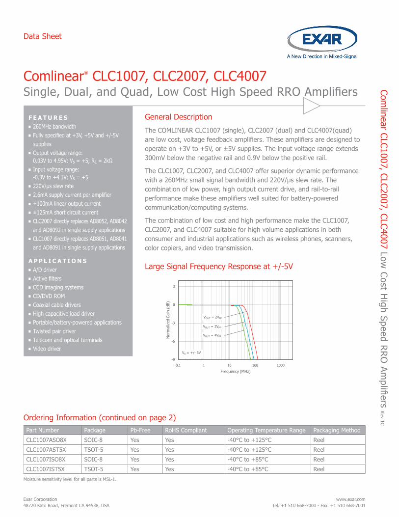
The COMLINEAR CLC1007 (single), CLC2007 (dual) and CLC4007(quad) are low cost, voltage feedback amplifiers. These amplifiers are designed to operate on +3V to +5V, or ±5V supplies. The input voltage range extends 300mV below the negative rail and 0.9V below the positive rail.
The CLC1007, CLC2007, and CLC4007 offer superior dynamic performance with a 260MHz small signal bandwidth and 220V/μs slew rate. The combination of low power, high output current drive, and rail-to-rail performance make these amplifiers well suited for battery-powered communication/computing systems.
The combination of low cost and high performance make the CLC1007, CLC2007, and CLC4007 suitable for high volume applications in both consumer and industrial applications such as wireless phones, scanners, color copiers, and video transmission.
Large Signal Frequency Response at +/-5V
Ordering Information (continued on page 2)Part Number Package Pb-Free RoHS Compliant Operating Temperature Range Packaging Method
CLC1007ASO8X SOIC-8 Yes Yes -40°C to +125°C Reel
CLC1007AST5X TSOT-5 Yes Yes -40°C to +125°C Reel
CLC1007ISO8X SOIC-8 Yes Yes -40°C to +85°C Reel
CLC1007IST5X TSOT-5 Yes Yes -40°C to +85°C Reel
Moisture sensitivity level for all parts is MSL-1.
-9
-6
-3
0
3
0.1 1 10 100 1000
Nor
mal
ized
Gai
n (d
B)
Frequency (MHz)
VS = +/- 5V
VOUT = 2VPP
VOUT = 3VPP
VOUT = 4VPP
Data SheetCom
linear CLC1007, CLC2007, CLC4007 Low C
ost High Speed R
RO
Amplifiers R
ev 1C
©2007-2013 Exar Corporation 2/25 Rev 1C
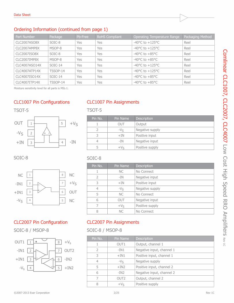
CLC1007 Pin Assignments
TSOT-5
Pin No. Pin Name Description
1 OUT Output
2 -VS Negative supply
3 +IN Positive input
4 -IN Negative input
5 +VS Positive supply
SOIC-8
Pin No. Pin Name Description
1 NC No Connect
2 -IN Negative input
3 +IN Positive input
4 -VS Negative supply
5 NC No Connect
6 OUT Negative input
7 +VS Positive supply
8 NC No Connect
CLC1007 Pin Configurations
2
3
5
4+IN
+VS
-IN
1
-VS
OUT
-+
2
3
4 5
6
7
8
+IN1
NC
OUT
NC
1
-IN1
NC
-VS
+VS
SOIC-8
TSOT-5
CLC2007 Pin Assignments
SOIC-8 / MSOP-8
Pin No. Pin Name Description
1 OUT1 Output, channel 1
2 -IN1 Negative input, channel 1
3 +IN1 Positive input, channel 1
4 -VS Negative supply
5 +IN2 Positive input, channel 2
6 -IN2 Negative input, channel 2
7 OUT2 Output, channel 2
8 +VS Positive supply
CLC2007 Pin Configuration
SOIC-8 / MSOP-8
-
+-
+
1
2
3
4
OUT1
-IN1
+IN1
-Vs
+Vs
OUT2
-IN2
+IN2
8
7
6
5
Ordering Information (continued from page 1)Part Number Package Pb-Free RoHS Compliant Operating Temperature Range Packaging Method
CLC2007ASO8X SOIC-8 Yes Yes -40°C to +125°C Reel
CLC2007AMP8X MSOP-8 Yes Yes -40°C to +125°C Reel
CLC2007ISO8X SOIC-8 Yes Yes -40°C to +85°C Reel
CLC2007IMP8X MSOP-8 Yes Yes -40°C to +85°C Reel
CLC4007ASO14X SOIC-14 Yes Yes -40°C to +125°C Reel
CLC4007ATP14X TSSOP-14 Yes Yes -40°C to +125°C Reel
CLC4007ISO14X SOIC-14 Yes Yes -40°C to +85°C Reel
CLC4007ITP14X TSSOP-14 Yes Yes -40°C to +85°C Reel
Moisture sensitivity level for all parts is MSL-1.
Data SheetCom
linear CLC1007, CLC2007, CLC4007 Low C
ost High Speed R
RO
Amplifiers R
ev 1C
©2007-2013 Exar Corporation 3/25 Rev 1C
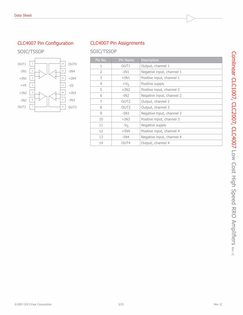
CLC4007 Pin Assignments
SOIC/TSSOP
Pin No. Pin Name Description
1 OUT1 Output, channel 1
2 -IN1 Negative input, channel 1
3 +IN1 Positive input, channel 1
4 +VS Positive supply
5 +IN2 Positive input, channel 2
6 -IN2 Negative input, channel 2
7 OUT2 Output, channel 2
8 OUT3 Output, channel 3
9 -IN3 Negative input, channel 3
10 +IN3 Positive input, channel 3
11 -VS Negative supply
12 +IN4 Positive input, channel 4
13 -IN4 Negative input, channel 4
14 OUT4 Output, channel 4
CLC4007 Pin Configuration
SOIC/TSSOP
Data SheetCom
linear CLC1007, CLC2007, CLC4007 Low C
ost High Speed R
RO
Amplifiers R
ev 1C
©2007-2013 Exar Corporation 4/25 Rev 1C
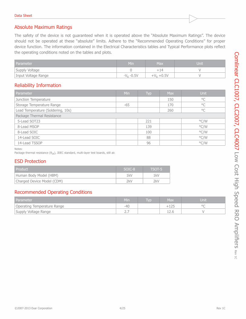
Absolute Maximum Ratings
The safety of the device is not guaranteed when it is operated above the “Absolute Maximum Ratings”. The device should not be operated at these “absolute” limits. Adhere to the “Recommended Operating Conditions” for proper device function. The information contained in the Electrical Characteristics tables and Typical Performance plots reflect the operating conditions noted on the tables and plots.
Parameter Min Max Unit
Supply Voltage 0 +14 VInput Voltage Range -Vs -0.5V +Vs +0.5V V
Reliability InformationParameter Min Typ Max Unit
Junction Temperature 150 °CStorage Temperature Range -65 170 °CLead Temperature (Soldering, 10s) 260 °CPackage Thermal Resistance5-Lead SOT23 221 °C/W8-Lead MSOP 139 °C/W8-Lead SOIC 100 °C/W14-Lead SOIC 88 °C/W14-Lead TSSOP 96 °C/W
Notes: Package thermal resistance (θJA), JDEC standard, multi-layer test boards, still air.
ESD ProtectionProduct SOIC-8 TSOT-5
Human Body Model (HBM) 1kV 1kV
Charged Device Model (CDM) 2kV 2kV
Recommended Operating ConditionsParameter Min Typ Max Unit
Operating Temperature Range -40 +125 °CSupply Voltage Range 2.7 12.6 V
Data SheetCom
linear CLC1007, CLC2007, CLC4007 Low C
ost High Speed R
RO
Amplifiers R
ev 1C
©2007-2013 Exar Corporation 5/25 Rev 1C
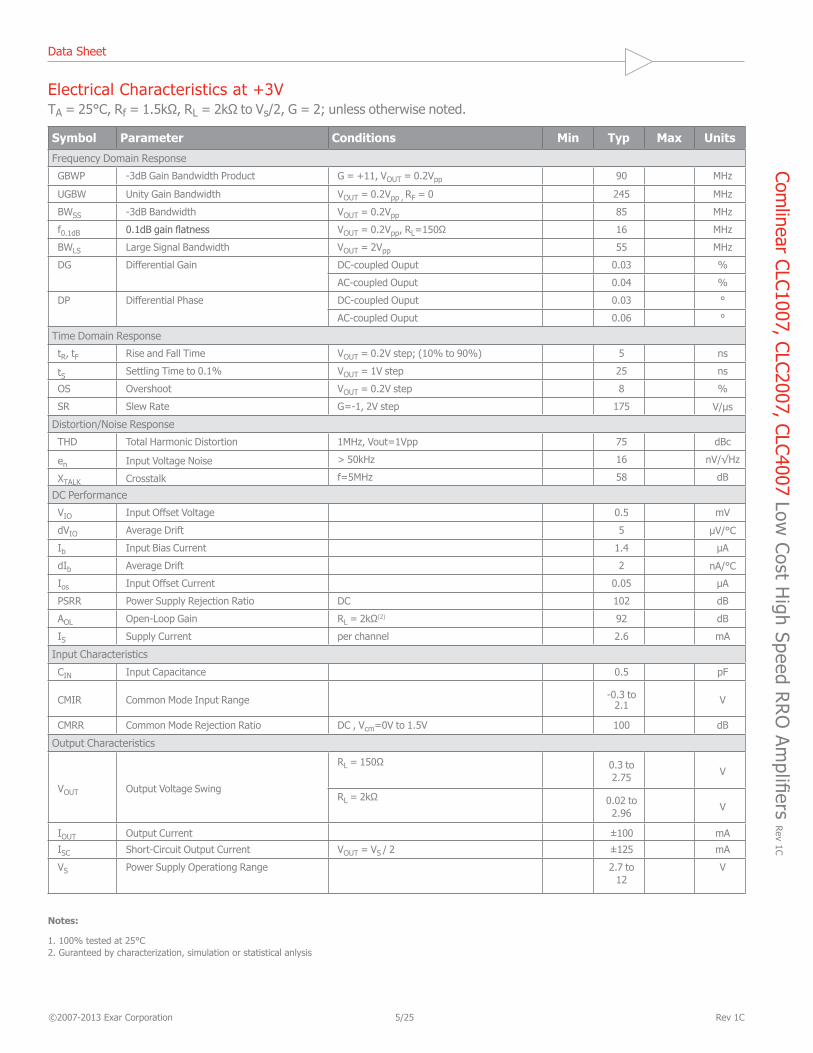
Electrical Characteristics at +3VTA = 25°C, Rf = 1.5kΩ, RL = 2kΩ to Vs/2, G = 2; unless otherwise noted.
Symbol Parameter Conditions Min Typ Max Units
Frequency Domain Response
GBWP -3dB Gain Bandwidth Product G = +11, VOUT = 0.2Vpp 90 MHz
UGBW Unity Gain Bandwidth VOUT = 0.2Vpp , RF = 0 245 MHz
BWSS -3dB Bandwidth VOUT = 0.2Vpp 85 MHz
f0.1dB 0.1dB gain flatness VOUT = 0.2Vpp, RL=150Ω 16 MHz
BWLS Large Signal Bandwidth VOUT = 2Vpp 55 MHz
DG Differential Gain DC-coupled Ouput 0.03 %
AC-coupled Ouput 0.04 %
DP Differential Phase DC-coupled Ouput 0.03 °
AC-coupled Ouput 0.06 °
Time Domain Response
tR, tF Rise and Fall Time VOUT = 0.2V step; (10% to 90%) 5 ns
tS Settling Time to 0.1% VOUT = 1V step 25 ns
OS Overshoot VOUT = 0.2V step 8 %
SR Slew Rate G=-1, 2V step 175 V/µs
Distortion/Noise Response
THD Total Harmonic Distortion 1MHz, Vout=1Vpp 75 dBc
en Input Voltage Noise > 50kHz 16 nV/√Hz
XTALK Crosstalk f=5MHz 58 dB
DC Performance
VIO Input Offset Voltage 0.5 mV
dVIO Average Drift 5 µV/°C
Ib Input Bias Current 1.4 μA
dIb Average Drift 2 nA/°C
Ios Input Offset Current 0.05 μA
PSRR Power Supply Rejection Ratio DC 102 dB
AOL Open-Loop Gain RL = 2kΩ(2) 92 dB
IS Supply Current per channel 2.6 mA
Input Characteristics
CIN Input Capacitance 0.5 pF
CMIR Common Mode Input Range -0.3 to 2.1 V
CMRR Common Mode Rejection Ratio DC , Vcm=0V to 1.5V 100 dB
Output Characteristics
VOUT Output Voltage Swing
RL = 150Ω 0.3 to 2.75 V
RL = 2kΩ 0.02 to 2.96 V
IOUT Output Current ±100 mA
ISC Short-Circuit Output Current VOUT = VS / 2 ±125 mA
VS Power Supply Operationg Range 2.7 to 12
V
Notes:
1. 100% tested at 25°C2. Guranteed by characterization, simulation or statistical anlysis

Data SheetCom
linear CLC1007, CLC2007, CLC4007 Low C
ost High Speed R
RO
Amplifiers R
ev 1C
©2007-2013 Exar Corporation 6/25 Rev 1C
Electrical Characteristics at +5VTA = 25°C, Rf = 1.5kΩ, RL = 2kΩ to Vs/2, G = 2; unless otherwise noted.
Symbol Parameter Conditions Min Typ Max Units
Frequency Domain Response
GBWP -3dB Gain Bandwidth Product G = +11, VOUT = 0.2Vpp 95 MHz
UGBW Unity Gain Bandwidth VOUT = 0.2Vpp , RF = 0 250 MHz
BWSS -3dB Bandwidth VOUT = 0.2Vpp 85 MHz
f0.1dB 0.1dB gain flatness VOUT = 0.2Vpp, RL=150Ω 35 MHz
BWLS Large Signal Bandwidth VOUT = 2Vpp 65 MHz
DG Differential Gain DC-coupled Ouput 0.03 %
AC-coupled Ouput 0.04 %
DP Differential Phase DC-coupled Ouput 0.03 °
AC-coupled Ouput 0.06 °
Time Domain Response
tR, tF Rise and Fall Time VOUT = 0.2V step 5 ns
tS Settling Time to 0.1% VOUT = 2V step 25 ns
OS Overshoot VOUT = 0.2V step 5 %
SR Slew Rate G=-1 , 4V step, 220 V/µs
Distortion/Noise Response
THD Total Harmonic Distortion 1MHz, VOUT=2VPP -75 dB
en Input Voltage Noise > 50kHz 16 nV/√Hz
XTALK Crosstalk f=5MHz 58 dB
DC Performance
VIO Input Offset Voltage(1) -7 0.5 7 mV
dVIO Average Drift 5 µV/°C
Ib Input Bias Current (1) -2 1.4 2 μA
dIb Average Drift 2 nA/°C
Ios Input Offset Current (1) -0.75 0.05 0.75 μA
PSRR Power Supply Rejection Ratio (1) DC 80 102 dB
AOL Open-Loop Gain RL = 2kΩ(2) 80 92 dB
IS Supply Current (1) per channel 2.6 4 mA
Input Characteristics
CIN Input Capacitance 0.5 pF
CMIR Common Mode Input Range -0.3 to 4.1 V
CMRR Common Mode Rejection Ratio (1) DC , Vcm= 0V to 3.5V 75 100 dB
Output Characteristics
VOUT Output Voltage Swing
RL = 150Ω(1) 4.65 0.1 to 4.9 0.35 V
RL = 2kΩ 0.03 to 4.95 V
IOUT Output Current ±100 mA
ISC Short-Circuit Output Current VOUT = VS / 2 ±125 mA
VS Power Supply Operationg Range 2.7 to 12
V
Notes:
1. 100% tested at 25°C2. Guranteed by characterization, simulation or statistical anlysis
Data SheetCom
linear CLC1007, CLC2007, CLC4007 Low C
ost High Speed R
RO
Amplifiers R
ev 1C
©2007-2013 Exar Corporation 7/25 Rev 1C
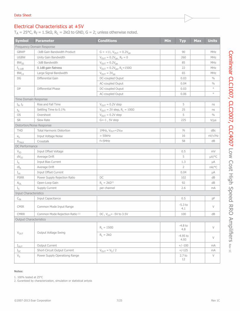
Electrical Characteristics at ±5VTA = 25°C, Rf = 1.5kΩ, RL = 2kΩ to GND, G = 2; unless otherwise noted.
Symbol Parameter Conditions Min Typ Max Units
Frequency Domain Response
GBWP -3dB Gain Bandwidth Product G = +11, VOUT = 0.2Vpp 90 MHz
UGBW Unity Gain Bandwidth VOUT = 0.2Vpp , RF = 0 260 MHz
BWSS -3dB Bandwidth VOUT = 0.2Vpp 85 MHz
f0.1dB 0.1dB gain flatness VOUT = 0.2Vpp, RL=150Ω 22 MHz
BWLS Large Signal Bandwidth VOUT = 2Vpp 65 MHz
DG Differential Gain DC-coupled Ouput 0.03 %
AC-coupled Ouput 0.04 %
DP Differential Phase DC-coupled Ouput 0.03 °
AC-coupled Ouput 0.06 °
Time Domain Response
tR, tF Rise and Fall Time VOUT = 0.2V step 5 ns
tS Settling Time to 0.1% VOUT = 2V step, RL = 100Ω 25 ns
OS Overshoot VOUT = 0.2V step 5 %
SR Slew Rate G=-1 , 5V step 225 V/µs
Distortion/Noise Response
THD Total Harmonic Distortion 1MHz, VOUT=2VPP 76 dBc
en Input Voltage Noise > 50kHz 16 nV/√Hz
XTALK Crosstalk f=5MHz 58 dB
DC Performance
VIO Input Offset Voltage 0.5 mV
dVIO Average Drift 5 µV/°C
Ib Input Bias Current 1.3 μA
dIb Average Drift 2 nA/°C
Ios Input Offset Current 0.04 μA
PSRR Power Supply Rejection Ratio DC 102 dB
AOL Open-Loop Gain RL = 2kΩ(2) 92 dB
IS Supply Current per channel 2.6 mA
Input Characteristics
CIN Input Capacitance 0.5 pF
CMIR Common Mode Input Range -5.3 to 4.1 V
CMRR Common Mode Rejection Ratio (1) DC , Vcm= -5V to 3.5V 100 dB
Output Characteristics
VOUT Output Voltage Swing
RL = 150Ω -4.8 to 4.8 V
RL = 2kΩ -4.95 to 4.93 V
IOUT Output Current +/ -100 mA
ISC Short-Circuit Output Current VOUT = VS / 2 +/-125 mA
VS Power Supply Operationg Range 2.7 to 12
V
Notes:
1. 100% tested at 25°C2. Guranteed by characterization, simulation or statistical anlysis
Data SheetCom
linear CLC1007, CLC2007, CLC4007 Low C
ost High Speed R
RO
Amplifiers R
ev 1C
©2007-2013 Exar Corporation 8/25 Rev 1C
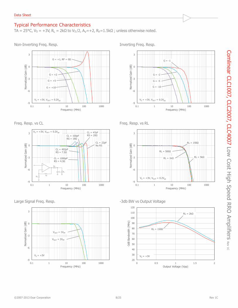
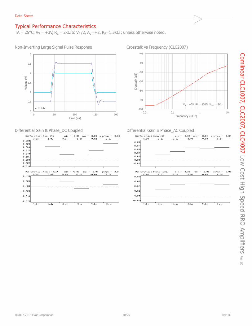
Typical Performance CharacteristicsTA = 25°C, VS = +3V, RL = 2kΩ to VS /2, AV=+2, RF=1.5kΩ ; unless otherwise noted.
-9
-6
-3
0
3
0.1 1 10 100 1000
Nor
mal
ized
Gai
n (d
B)
Frequency (MHz)
G = -1
G = -5
G = -10
VS = +3V, VOUT = 0.2Vpp
G = -2
-9
-6
-3
0
3
0.1 1 10 100 1000
Nor
mal
ized
Gai
n (d
B)
Frequency (MHz)
G = +1, RF = 0Ω
G = +5
G = +10
VS = +3V, VOUT = 0.2Vpp
G = +2
-9
-6
-3
0
3
0.1 1 10 100 1000
Nor
mal
ized
Gai
n (d
B)
Frequency (MHz)
RL = 150Ω
VS = +3V, VOUT = 0.2Vpp
RL = 500Ω
RL = 1kΩ RL = 5kΩ
-9
-6
-3
0
3
0.1 1 10 100 1000
Nor
mal
ized
Gai
n (d
B)
Frequency (MHz)
CL = 22pFNo RS
VS = +3V, VOUT = 0.2Vpp CL = 47pFRS = 20ΩCL = 100pF
RS = 18Ω
CL = 492pFRS = 7.5Ω
CL = 1000pFRS = 4.3Ω
20
30
40
50
60
70
80
90
100
110
120
0 0.5 1 1.5 2
-3dB
Ban
dwid
th (
MH
z)
Output Voltage (Vpp)
RL = 150Ω
VS = +3V
RL = 2kΩ
-9
-6
-3
0
3
0.1 1 10 100 1000
Nor
mal
ized
Gai
n (d
B)
Frequency (MHz)
VS = +3V
VOUT = 1VPP
VOUT = 2VPP
Non-Inverting Freq. Resp. Inverting Freq. Resp.
Freq. Resp. vs CL Freq. Resp. vs RL
Large Signal Freq. Resp. -3db BW vs Output Voltage
+
-RLCL
RFRG
RS
Data SheetCom
linear CLC1007, CLC2007, CLC4007 Low C
ost High Speed R
RO
Amplifiers R
ev 1C
©2007-2013 Exar Corporation 9/25 Rev 1C
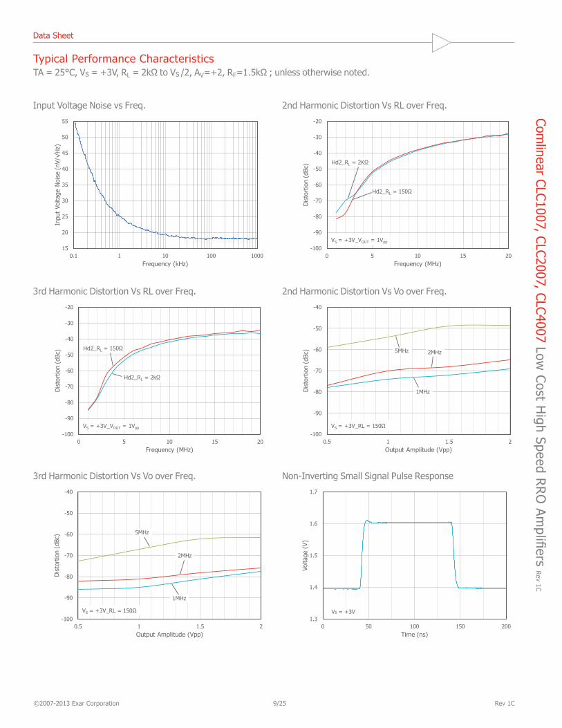
Typical Performance CharacteristicsTA = 25°C, VS = +3V, RL = 2kΩ to VS /2, AV=+2, RF=1.5kΩ ; unless otherwise noted.
-100
-90
-80
-70
-60
-50
-40
-30
-20
0 5 10 15 20
Dis
tort
ion
(dBc
)
Frequency (MHz)
Hd2_RL = 2KΩ
VS = +3V_VOUT = 1Vpp
Hd2_RL = 150Ω
15
20
25
30
35
40
45
50
55
0.1 1 10 100 1000
Inpu
t Vo
ltage
Noi
se (
nV/√
Hz)
Frequency (kHz)
-100
-90
-80
-70
-60
-50
-40
0.5 1 1.5 2
Dis
tort
ion
(dBc
)
Output Amplitude (Vpp)
1MHz
VS = +3V_RL = 150Ω
2MHz5MHz
-100
-90
-80
-70
-60
-50
-40
-30
-20
0 5 10 15 20
Dis
tort
ion
(dBc
)
Frequency (MHz)
Hd2_RL = 150Ω
VS = +3V_VOUT = 1Vpp
Hd2_RL = 2kΩ
1.3
1.4
1.5
1.6
1.7
0 50 100 150 200
Volta
ge (
V)
Time (ns)
Vs = +3V-100
-90
-80
-70
-60
-50
-40
0.5 1 1.5 2
Dis
tort
ion
(dBc
)
Output Amplitude (Vpp)
1MHz
VS = +3V_RL = 150Ω
2MHz
5MHz
3rd Harmonic Distortion Vs RL over Freq. 2nd Harmonic Distortion Vs Vo over Freq.
3rd Harmonic Distortion Vs Vo over Freq. Non-Inverting Small Signal Pulse Response
Input Voltage Noise vs Freq. 2nd Harmonic Distortion Vs RL over Freq.
Data SheetCom
linear CLC1007, CLC2007, CLC4007 Low C
ost High Speed R
RO
Amplifiers R
ev 1C
©2007-2013 Exar Corporation 10/25 Rev 1C
Typical Performance CharacteristicsTA = 25°C, VS = +3V, RL = 2kΩ to VS /2, AV=+2, RF=1.5kΩ ; unless otherwise noted.
-100
-90
-80
-70
-60
-50
-40
0.01 0.1 1 10
Cros
stal
k (d
B)
Frequency (MHz)
VS = +3V, RL = 150Ω, VOUT = 2VPP
0
0.5
1
1.5
2
2.5
3
0 50 100 150 200
Volta
ge (
V)
Time (ns)
Vs = +3V
Non-Inverting Large Signal Pulse Response Crosstalk vs Frequency (CLC2007)
Differential Gain & Phase_DC Coupled Differential Gain & Phase_AC Coupled
Data SheetCom
linear CLC1007, CLC2007, CLC4007 Low C
ost High Speed R
RO
Amplifiers R
ev 1C
©2007-2013 Exar Corporation 11/25 Rev 1C
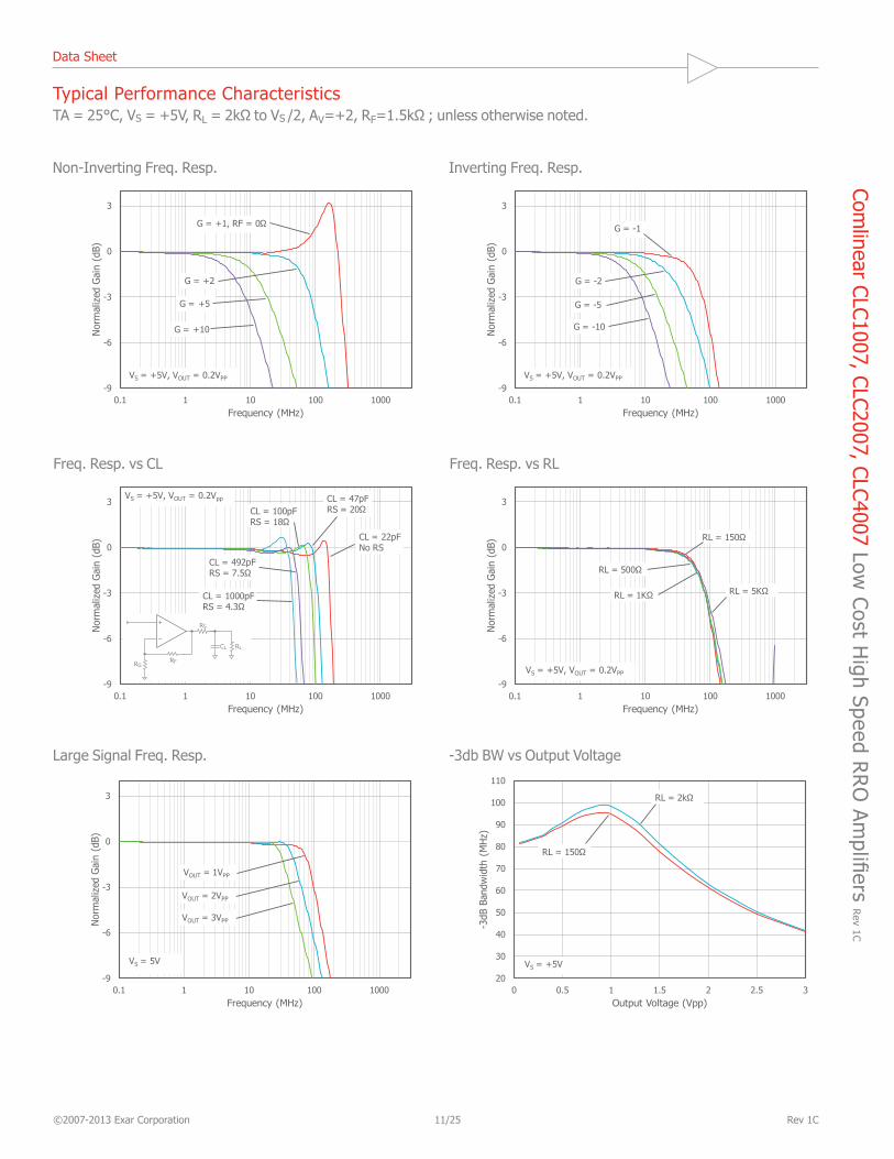
Typical Performance CharacteristicsTA = 25°C, VS = +5V, RL = 2kΩ to VS /2, AV=+2, RF=1.5kΩ ; unless otherwise noted.
Large Signal Freq. Resp. -3db BW vs Output Voltage
-9
-6
-3
0
3
0.1 1 10 100 1000
Nor
mal
ized
Gai
n (d
B)
Frequency (MHz)
G = -1
G = -5
G = -10
VS = +5V, VOUT = 0.2VPP
G = -2
-9
-6
-3
0
3
0.1 1 10 100 1000
Nor
mal
ized
Gai
n (d
B)
Frequency (MHz)
G = +1, RF = 0Ω
G = +5
G = +10
VS = +5V, VOUT = 0.2VPP
G = +2
-9
-6
-3
0
3
0.1 1 10 100 1000
Nor
mal
ized
Gai
n (d
B)
Frequency (MHz)
RL = 150Ω
VS = +5V, VOUT = 0.2VPP
RL = 500Ω
RL = 1KΩ RL = 5KΩ
-9
-6
-3
0
3
0.1 1 10 100 1000
Nor
mal
ized
Gai
n (d
B)
Frequency (MHz)
CL = 22pFNo RS
VS = +5V, VOUT = 0.2Vpp CL = 47pFRS = 20ΩCL = 100pF
RS = 18Ω
CL = 492pFRS = 7.5Ω
CL = 1000pFRS = 4.3Ω
20
30
40
50
60
70
80
90
100
110
0 0.5 1 1.5 2 2.5 3
-3dB
Ban
dwid
th (
MH
z)
Output Voltage (Vpp)
RL = 150Ω
VS = +5V
RL = 2kΩ
-9
-6
-3
0
3
0.1 1 10 100 1000
Nor
mal
ized
Gai
n (d
B)
Frequency (MHz)
VS = 5V
VOUT = 1VPP
VOUT = 2VPP
VOUT = 3VPP
Non-Inverting Freq. Resp. Inverting Freq. Resp.
Freq. Resp. vs CL Freq. Resp. vs RL
+
-RLCL
RFRG
RS
Data SheetCom
linear CLC1007, CLC2007, CLC4007 Low C
ost High Speed R
RO
Amplifiers R
ev 1C
©2007-2013 Exar Corporation 12/25 Rev 1C
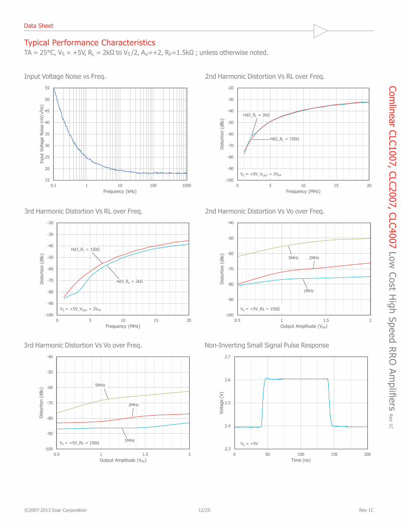
Typical Performance CharacteristicsTA = 25°C, VS = +5V, RL = 2kΩ to VS /2, AV=+2, RF=1.5kΩ ; unless otherwise noted.
Input Voltage Noise vs Freq. 2nd Harmonic Distortion Vs RL over Freq.
-100
-90
-80
-70
-60
-50
-40
-30
-20
0 5 10 15 20
Dis
tort
ion
(dBc
)
Frequency (MHz)
Hd2_RL = 2kΩ
VS = +5V_VOUT = 2VPP
Hd2_RL = 150Ω
15
20
25
30
35
40
45
50
55
0.1 1 10 100 1000
Inpu
t Vo
ltage
Noi
se (
nV/√
Hz)
Frequency (kHz)
-100
-90
-80
-70
-60
-50
-40
0.5 1 1.5 2
Dis
tort
ion
(dBc
)
Output Amplitude (VPP)
1MHz
VS = +5V_RL = 150Ω
2MHz5MHz
-100
-90
-80
-70
-60
-50
-40
-30
-20
0 5 10 15 20
Dis
tort
ion
(dBc
)
Frequency (MHz)
Hd3_RL = 150Ω
Vs = +/-5V_VOUT = 2Vpp
Hd3_RL = 2kΩ
VS = +5V_VOUT = 2VPP
2.3
2.4
2.5
2.6
2.7
0 50 100 150 200
Volta
ge (
V)
Time (ns)
VS = +5V-100
-90
-80
-70
-60
-50
-40
0.5 1 1.5 2
Dis
tort
ion
(dBc
)
Output Amplitude (VPP)
1MHzVs = +5V_RL = 150Ω
2MHz
5MHz
VS = +5V_RL = 150Ω
3rd Harmonic Distortion Vs RL over Freq. 2nd Harmonic Distortion Vs Vo over Freq.
3rd Harmonic Distortion Vs Vo over Freq. Non-Inverting Small Signal Pulse Response
Data SheetCom
linear CLC1007, CLC2007, CLC4007 Low C
ost High Speed R
RO
Amplifiers R
ev 1C
©2007-2013 Exar Corporation 13/25 Rev 1C
Typical Performance CharacteristicsTA = 25°C, VS = +5V, RL = 2kΩ to VS /2, AV=+2, RF=1.5kΩ ; unless otherwise noted.
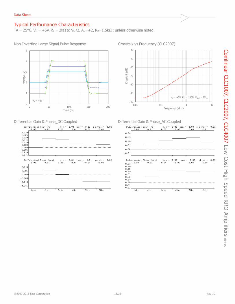
Non-Inverting Large Signal Pulse Response Crosstalk vs Frequency (CLC2007)
-100
-90
-80
-70
-60
-50
-40
0.01 0.1 1 10
Cros
stal
k (d
B)
Frequency (MHz)
VS = +5V, RL = 150Ω, VOUT = 2Vpp
0
1
2
3
4
5
0 50 100 150 200
Volta
ge (
V)
Time (ns)
VS = +5V
Differential Gain & Phase_DC Coupled Differential Gain & Phase_AC Coupled
Data SheetCom
linear CLC1007, CLC2007, CLC4007 Low C
ost High Speed R
RO
Amplifiers R
ev 1C
©2007-2013 Exar Corporation 14/25 Rev 1C
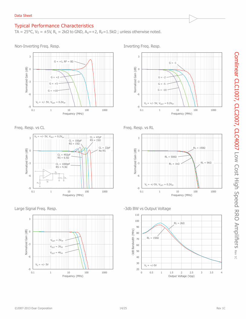
Typical Performance CharacteristicsTA = 25°C, VS = ±5V, RL = 2kΩ to GND, AV=+2, RF=1.5kΩ ; unless otherwise noted.
Non-Inverting Freq. Resp. Inverting Freq. Resp.
-9
-6
-3
0
3
0.1 1 10 100 1000
Nor
mal
ized
Gai
n (d
B)
Frequency (MHz)
G = -1
G = -5
G = -10
VS = +/- 5V, VOUT = 0.2VPP
G = -2
-9
-6
-3
0
3
0.1 1 10 100 1000
Nor
mal
ized
Gai
n (d
B)
Frequency (MHz)
G = +1, RF = 0Ω
G = +5
G = +10
VS = +/- 5V, VOUT = 0.2VPP
G = +2
-9
-6
-3
0
3
0.1 1 10 100 1000
Nor
mal
ized
Gai
n (d
B)
Frequency (MHz)
RL = 150Ω
VS = +/-5V, VOUT = 0.2VPP
RL = 500Ω
RL = 1kΩ RL = 5KΩ
-9
-6
-3
0
3
0.1 1 10 100 1000
Nor
mal
ized
Gai
n (d
B)
Frequency (MHz)
CL = 22pFNo RS
VS = +/- 5V, VOUT = 0.2Vpp CL = 47pFRS = 15ΩCL = 100pF
RS = 15Ω
CL = 492pFRS = 6.5Ω
CL = 1000pFRS = 4.3Ω
20
30
40
50
60
70
80
90
100
110
0 0.5 1 1.5 2 2.5 3 3.5 4
-3dB
Ban
dwid
th (
MH
z)
Output Voltage (Vpp)
RL = 150Ω
VS = +/-5V
RL = 2kΩ
-9
-6
-3
0
3
0.1 1 10 100 1000
Nor
mal
ized
Gai
n (d
B)
Frequency (MHz)
VS = +/- 5V
VOUT = 2VPP
VOUT = 3VPP
VOUT = 4VPP
Freq. Resp. vs CL Freq. Resp. vs RL
Large Signal Freq. Resp. -3db BW vs Output Voltage
+
-RLCL
RFRG
RS
Data SheetCom
linear CLC1007, CLC2007, CLC4007 Low C
ost High Speed R
RO
Amplifiers R
ev 1C
©2007-2013 Exar Corporation 15/25 Rev 1C
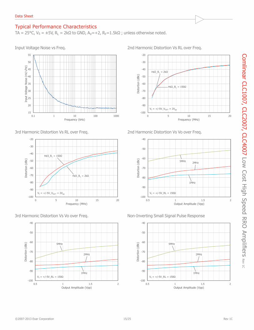
Typical Performance CharacteristicsTA = 25°C, VS = ±5V, RL = 2kΩ to GND, AV=+2, RF=1.5kΩ ; unless otherwise noted.
Input Voltage Noise vs Freq. 2nd Harmonic Distortion Vs RL over Freq.
-100
-90
-80
-70
-60
-50
-40
-30
-20
0 5 10 15 20
Dis
tort
ion
(dBc
)
Frequency (MHz)
Hd2_RL = 2kΩ
VS = +/-5V_VOUT = 2Vpp
Hd2_RL = 150Ω
15
20
25
30
35
40
45
50
55
0.1 1 10 100 1000
Inpu
t Vo
ltage
Noi
se (
nV/√
Hz)
Frequency (kHz)
-100
-90
-80
-70
-60
-50
-40
0.5 1 1.5 2
Dis
tort
ion
(dBc
)
Output Amplitude (Vpp)
1MHz
VS = +/-5V_RL = 150Ω
2MHz5MHz
-100
-90
-80
-70
-60
-50
-40
-30
-20
0 5 10 15 20
Dis
tort
ion
(dBc
)
Frequency (MHz)
Hd3_RL = 150Ω
Vs = +/-5V_VOUT = 2Vpp
Hd3_RL = 2kΩ
VS = +/-5V_VOUT = 2Vpp
-100
-90
-80
-70
-60
-50
-40
0.5 1 1.5 2
Dis
tort
ion
(dBc
)
Output Amplitude (Vpp)
1MHz
2MHz
5MHz
VS = +/-5V_RL = 150Ω-100
-90
-80
-70
-60
-50
-40
0.5 1 1.5 2
Dis
tort
ion
(dBc
)
Output Amplitude (Vpp)
1MHz
2MHz
5MHz
VS = +/-5V_RL = 150Ω
3rd Harmonic Distortion Vs RL over Freq. 2nd Harmonic Distortion Vs Vo over Freq.
3rd Harmonic Distortion Vs Vo over Freq. Non-Inverting Small Signal Pulse Response
Data SheetCom
linear CLC1007, CLC2007, CLC4007 Low C
ost High Speed R
RO
Amplifiers R
ev 1C
©2007-2013 Exar Corporation 16/25 Rev 1C
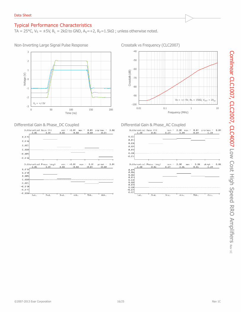
Typical Performance CharacteristicsTA = 25°C, VS = ±5V, RL = 2kΩ to GND, AV=+2, RF=1.5kΩ ; unless otherwise noted.
Non-Inverting Large Signal Pulse Response Crosstalk vs Frequency (CLC2007)
-100
-90
-80
-70
-60
-50
-40
0.01 0.1 1 10
Cros
stal
k (d
B)
Frequency (MHz)
Vs = +/- 5V, RL = 150Ω, VOUT = 2Vpp
-3
-2
-1
0
1
2
3
0 50 100 150 200
Volta
ge (
V)
Time (ns)
VS = +/-5V
Differential Gain & Phase_DC Coupled Differential Gain & Phase_AC Coupled
Data SheetCom
linear CLC1007, CLC2007, CLC4007 Low C
ost High Speed R
RO
Amplifiers R
ev 1C
©2007-2013 Exar Corporation 17/25 Rev 1C
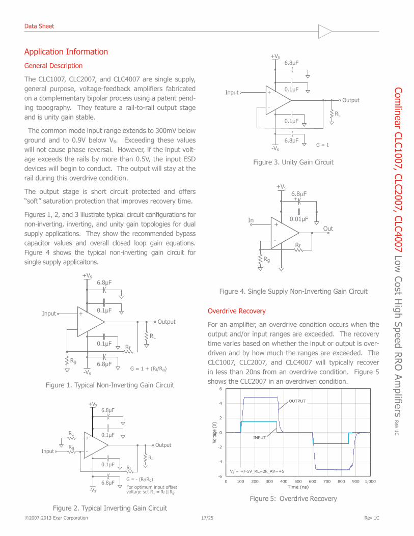
Application Information
General Description
The CLC1007, CLC2007, and CLC4007 are single supply, general purpose, voltage-feedback amplifiers fabricated on a complementary bipolar process using a patent pend-ing topography. They feature a rail-to-rail output stage and is unity gain stable.
The common mode input range extends to 300mV below ground and to 0.9V below Vs. Exceeding these values will not cause phase reversal. However, if the input volt-age exceeds the rails by more than 0.5V, the input ESD devices will begin to conduct. The output will stay at the rail during this overdrive condition.
The output stage is short circuit protected and offers “soft” saturation protection that improves recovery time.
Figures 1, 2, and 3 illustrate typical circuit configurations for non-inverting, inverting, and unity gain topologies for dual supply applications. They show the recommended bypass capacitor values and overall closed loop gain equations. Figure 4 shows the typical non-inverting gain circuit for single supply applicaitons.
+
-
Rf
0.1µF
6.8µF
Output
G = 1 + (Rf/Rg)
Input
+Vs
-Vs
Rg
0.1µF
6.8µF
RL
Figure 1. Typical Non-Inverting Gain Circuit
+
-
Rf
0.1µF
6.8µF
Output
G = - (Rf/Rg)
For optimum input offsetvoltage set R1 = Rf || Rg
Input
+Vs
-Vs
0.1µF
6.8µF
RL
Rg
R1
Figure 2. Typical Inverting Gain Circuit
+
-
0.1µF
6.8µF
Output
G = 1
Input
+Vs
-Vs
0.1µF
6.8µF
RL
Figure 3. Unity Gain Circuit
+
-Rf
0.01µF
6.8μF
OutIn
+Vs
+
Rg
Figure 4. Single Supply Non-Inverting Gain Circuit
Overdrive Recovery
For an amplifier, an overdrive condition occurs when the output and/or input ranges are exceeded. The recovery time varies based on whether the input or output is over-driven and by how much the ranges are exceeded. The CLC1007, CLC2007, and CLC4007 will typically recover in less than 20ns from an overdrive condition. Figure 5 shows the CLC2007 in an overdriven condition.
-6
-4
-2
0
2
4
6
0 100 200 300 400 500 600 700 800 900 1,000
Volta
ge (
V)
Time (ns)
VS = +/-5V_RL=2k_AV=+5
INPUT
OUTPUT
Figure 5: Overdrive Recovery
Data SheetCom
linear CLC1007, CLC2007, CLC4007 Low C
ost High Speed R
RO
Amplifiers R
ev 1C
©2007-2013 Exar Corporation 18/25 Rev 1C
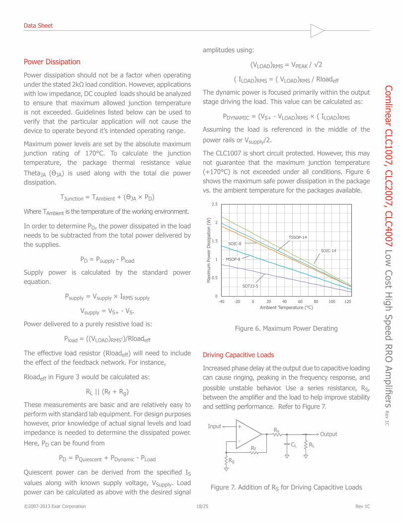
Power Dissipation
Power dissipation should not be a factor when operating under the stated 2kΩ load condition. However, applications with low impedance, DC coupled loads should be analyzed to ensure that maximum allowed junction temperature is not exceeded. Guidelines listed below can be used to verify that the particular application will not cause the device to operate beyond it’s intended operating range.
Maximum power levels are set by the absolute maximum junction rating of 170°C. To calculate the junction temperature, the package thermal resistance value
ThetaJA (ӨJA) is used along with the total die power dissipation.
TJunction = TAmbient + (ӨJA × PD)
Where TAmbient is the temperature of the working environment.
In order to determine PD, the power dissipated in the load needs to be subtracted from the total power delivered by the supplies.
PD = Psupply - Pload
Supply power is calculated by the standard power equation.
Psupply = Vsupply × IRMS supply
Vsupply = VS+ - VS-
Power delivered to a purely resistive load is:
Pload = ((VLOAD)RMS2)/Rloadeff
The effective load resistor (Rloadeff) will need to include the effect of the feedback network. For instance,
Rloadeff in Figure 3 would be calculated as:
RL || (Rf + Rg)
These measurements are basic and are relatively easy to perform with standard lab equipment. For design purposes however, prior knowledge of actual signal levels and load impedance is needed to determine the dissipated power.
Here, PD can be found from
PD = PQuiescent + PDynamic - PLoad
Quiescent power can be derived from the specified IS
values along with known supply voltage, VSupply. Load power can be calculated as above with the desired signal
amplitudes using:
(VLOAD)RMS = VPEAK / √2
( ILOAD)RMS = ( VLOAD)RMS / Rloadeff
The dynamic power is focused primarily within the output stage driving the load. This value can be calculated as:
PDYNAMIC = (VS+ - VLOAD)RMS × ( ILOAD)RMS
Assuming the load is referenced in the middle of the
power rails or Vsupply/2.
The CLC1007 is short circuit protected. However, this may not guarantee that the maximum junction temperature (+170°C) is not exceeded under all conditions. Figure 6 shows the maximum safe power dissipation in the package vs. the ambient temperature for the packages available.
0
0.5
1
1.5
2
2.5
-40 -20 0 20 40 60 80 100 120
Max
imum
Pow
er D
issi
patio
n (W
)
Ambient Temperature (°C)
SOT23-5
SOIC-8
MSOP-8
SOIC-14
TSSOP-14
Figure 6. Maximum Power Derating
Driving Capacitive Loads
Increased phase delay at the output due to capacitive loading can cause ringing, peaking in the frequency response, and
possible unstable behavior. Use a series resistance, RS, between the amplifier and the load to help improve stability and settling performance. Refer to Figure 7.
+
-Rf
InputOutput
Rg
Rs
CL RL
Figure 7. Addition of RS for Driving Capacitive Loads
Data SheetCom
linear CLC1007, CLC2007, CLC4007 Low C
ost High Speed R
RO
Amplifiers R
ev 1C
©2007-2013 Exar Corporation 19/25 Rev 1C
Table 1 provides the recommended RS for various capacitive
loads. The recommended RS values result in approximately <1dB peaking in the frequency response.
CL (Pf) Rs (Ω) -3db BW (MHz)
22pF 0 118
47pF 15 112
100pF 15 91
492pF 6.5 59
Table 1: Recommended RS vs. CL
For a given load capacitance, adjust RS to optimize the tradeoff between settling time and bandwidth. In general,
reducing RS will increase bandwidth at the expense of additional overshoot and ringing.
Layout Considerations
General layout and supply bypassing play major roles in high frequency performance. CADEKA has evaluation boards to use as a guide for high frequency layout and as an aid in device testing and characterization. Follow the steps below as a basis for high frequency layout:
Include 6.8µF and 0.1µF ceramic capacitors for power supply decoupling
Place the 6.8µF capacitor within 0.75 inches of the power pin
Place the 0.1µF capacitor within 0.1 inches of the power pin
Remove the ground plane under and around the part, especially near the input and output pins to reduce parasitic capacitance
Minimize all trace lengths to reduce series inductances
Refer to the evaluation board layouts below for more information.
Evaluation Board Information
The following evaluation boards are available to aid in the testing and layout of these devices:
Evaluation Board # ProductsCEB002 CLC1007 in TSOTCEB003 CLC1007 in SOICCEB006 CLC2007 in SOICCEB010 CLC2007 in MSOPCEB018 CLC4007 in SOIC
Evaluation Board Schematics
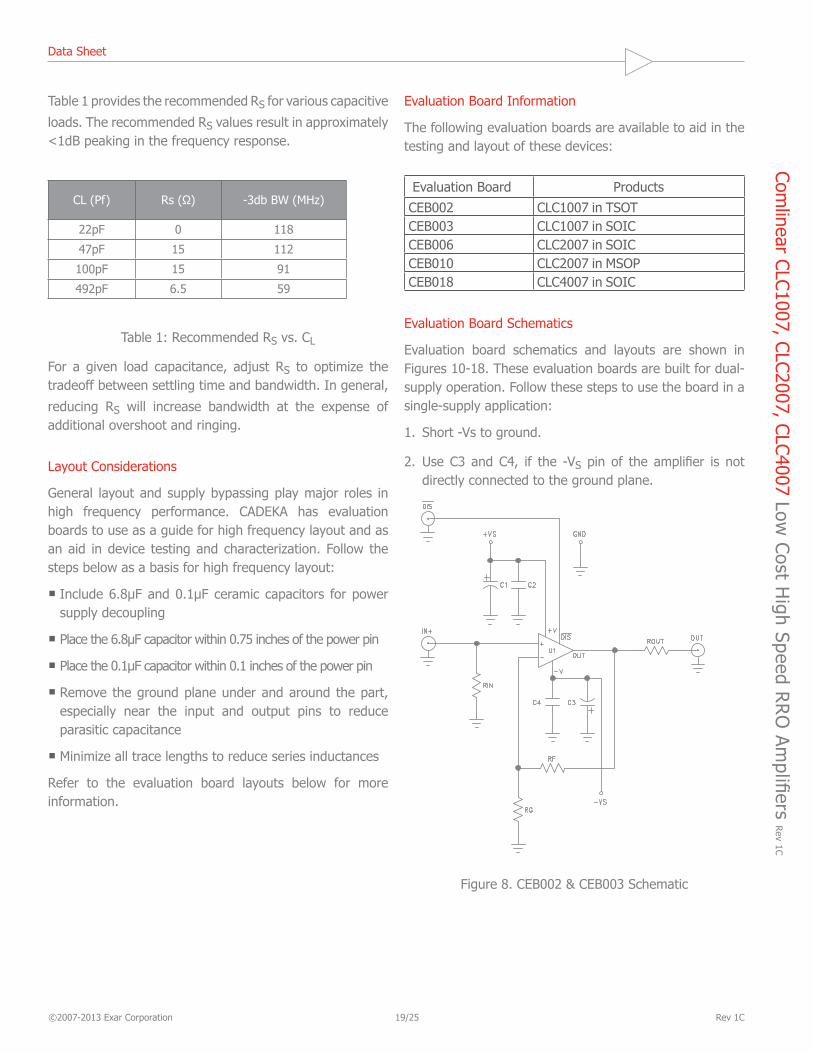
Evaluation board schematics and layouts are shown in Figures 10-18. These evaluation boards are built for dual- supply operation. Follow these steps to use the board in a single-supply application:
1. Short -Vs to ground.
2. Use C3 and C4, if the -VS pin of the amplifier is not directly connected to the ground plane.
Figure 8. CEB002 & CEB003 Schematic
Data SheetCom
linear CLC1007, CLC2007, CLC4007 Low C
ost High Speed R
RO
Amplifiers R
ev 1C
©2007-2013 Exar Corporation 20/25 Rev 1C
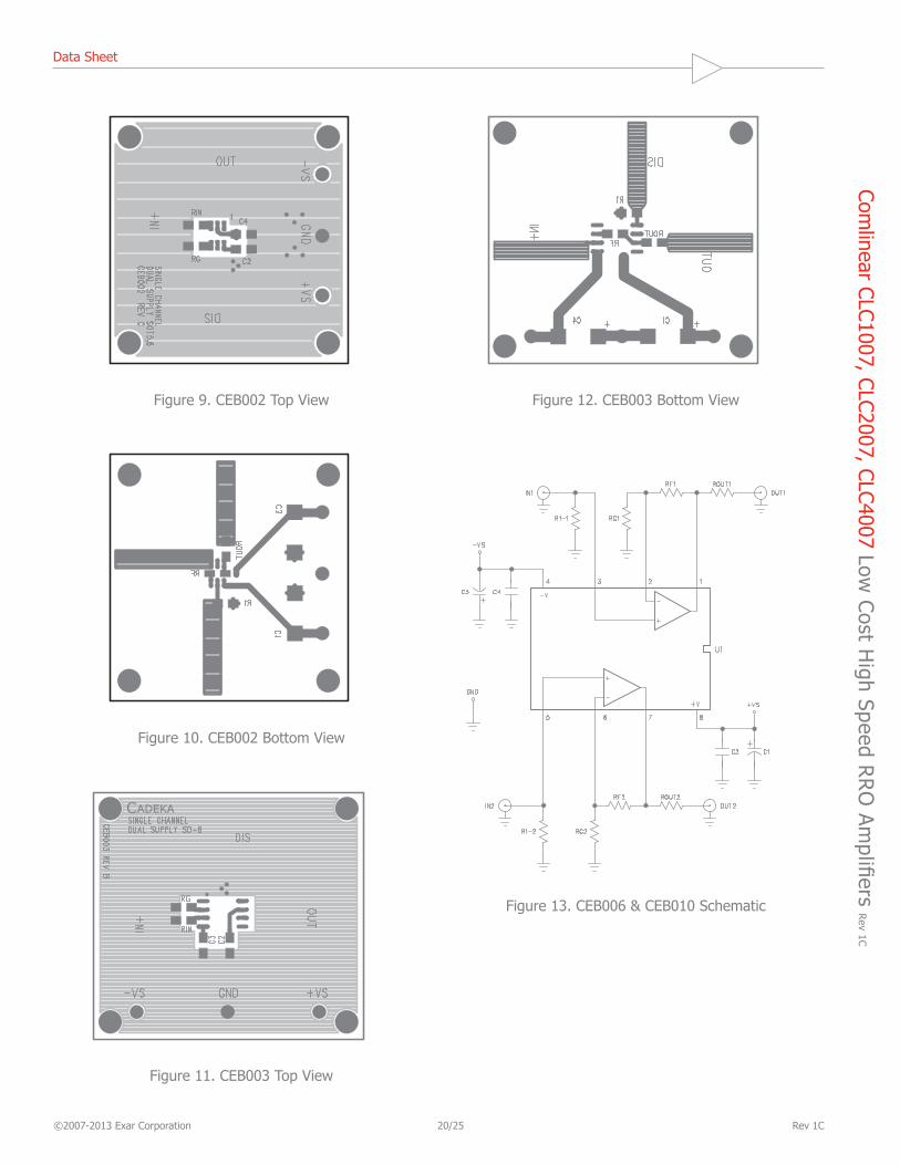
Figure 9. CEB002 Top View
Figure 10. CEB002 Bottom View
Figure 11. CEB003 Top View
Figure 12. CEB003 Bottom View
Figure 13. CEB006 & CEB010 Schematic
Data SheetCom
linear CLC1007, CLC2007, CLC4007 Low C
ost High Speed R
RO
Amplifiers R
ev 1C
©2007-2013 Exar Corporation 21/25 Rev 1C
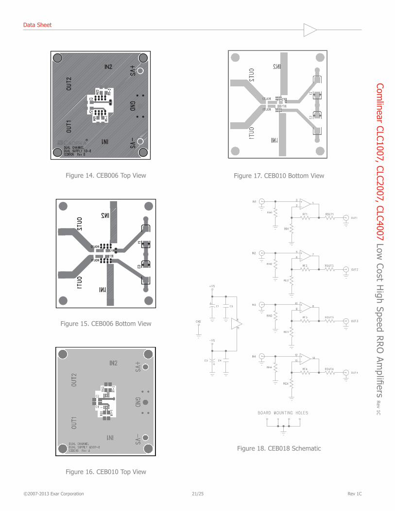
Figure 14. CEB006 Top View
Figure 15. CEB006 Bottom View
Figure 16. CEB010 Top View
Figure 17. CEB010 Bottom View
Figure 18. CEB018 Schematic
Data SheetCom
linear CLC1007, CLC2007, CLC4007 Low C
ost High Speed R
RO
Amplifiers R
ev 1C
©2007-2013 Exar Corporation 22/25 Rev 1C
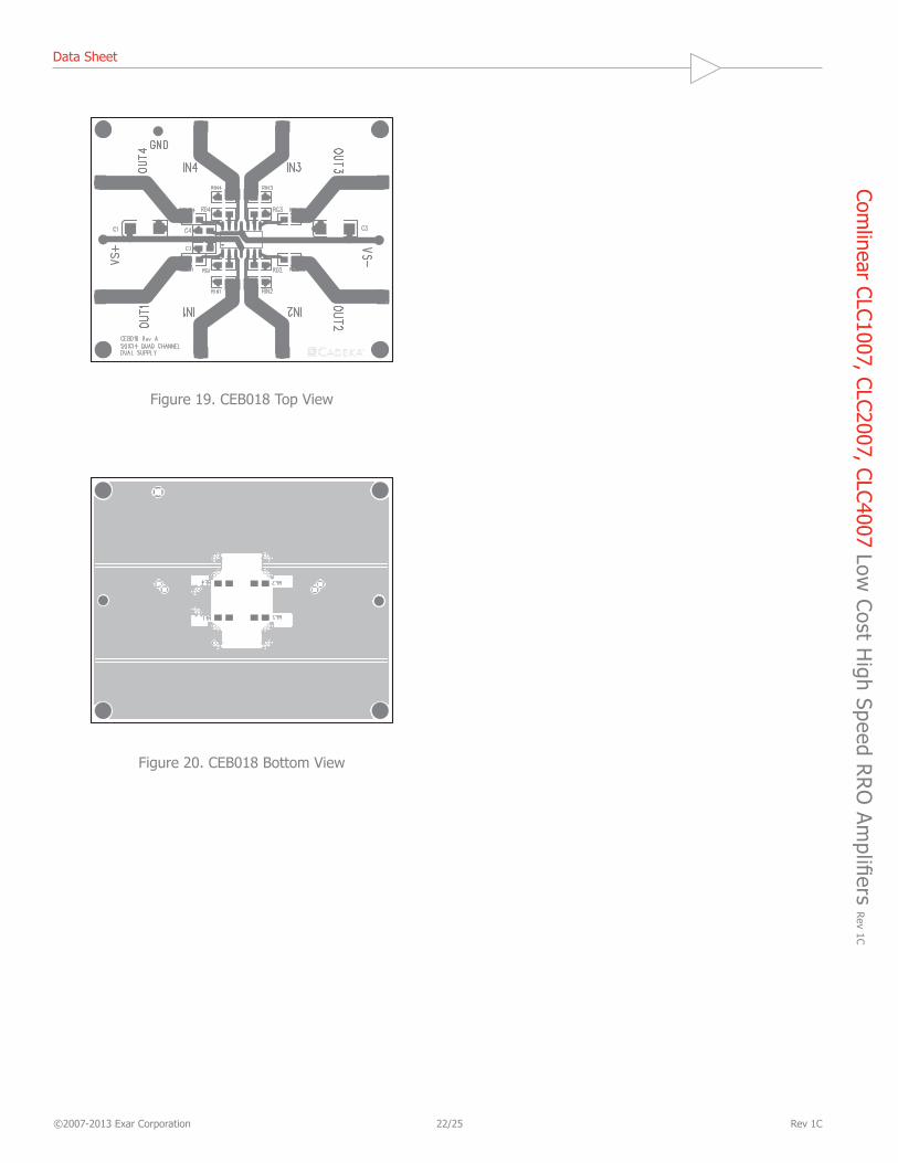
Figure 19. CEB018 Top View
Figure 20. CEB018 Bottom View
Data SheetCom
linear CLC1007, CLC2007, CLC4007 Low C
ost High Speed R
RO
Amplifiers R
ev 1C
©2007-2013 Exar Corporation 23/25 Rev 1C
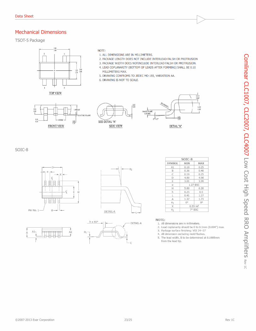
Mechanical Dimensions
TSOT-5 Package
SOIC-8
Data SheetCom
linear CLC1007, CLC2007, CLC4007 Low C
ost High Speed R
RO
Amplifiers R
ev 1C
©2007-2013 Exar Corporation 24/25 Rev 1C
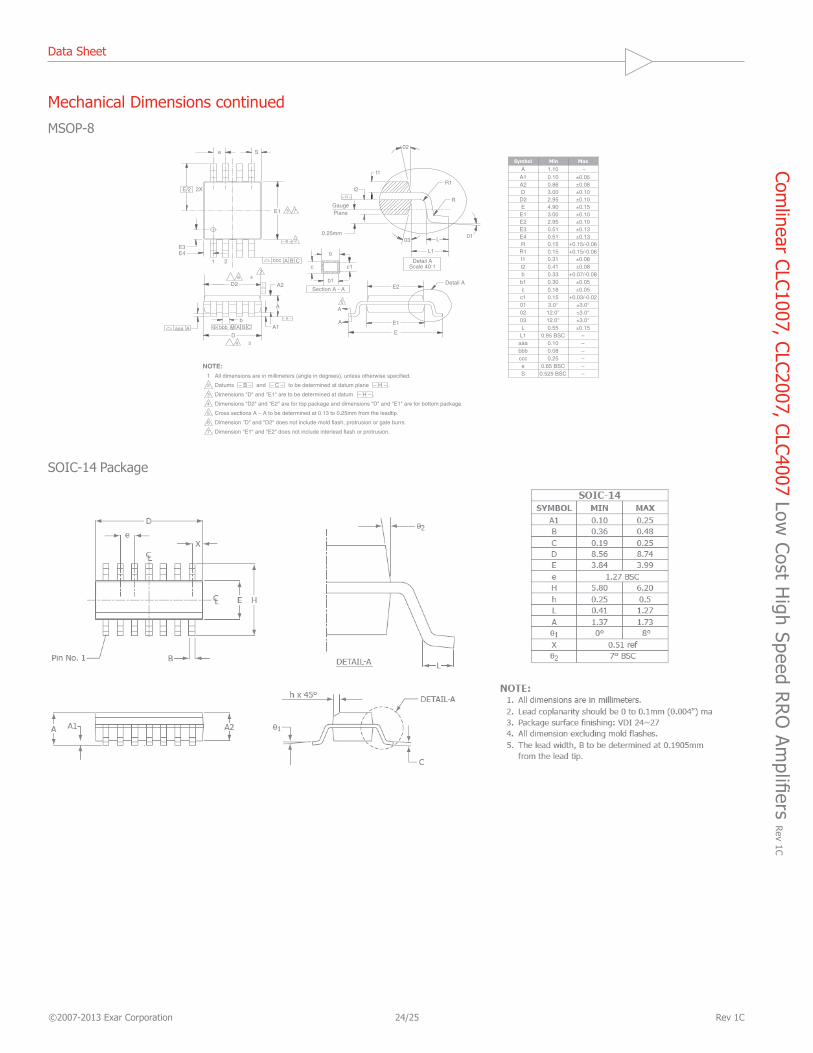
Mechanical Dimensions continued
MSOP-8
±±±±±±±±±
±±
±±
° ±3.0°° ±3.0°° ±3.0°
±
Ð
2
3
4
5
6
7 Dimension "E1" and "E2" does not include interlead flash or protrusion.
e S
E/2 2X
ccc A B C
Ð B Ð 2
3 7
26 4
D2 A2
A
A1Ð A Ð
ÐC
Ð
bbb A B CM
4 3
aaa A
E1
E2
E1E
Detail A
A
A
Section A - A
b
c c1
b1
Scale 40:1
t1
t2
Plane
0.25mm
R1
R
L
L1
03
02
01
Ð H Ð
E3E4
1 2
b
D
5
Symbol Min Max
SOIC-14 Package
Data SheetCom
linear CLC1007, CLC2007, CLC4007 Low C
ost High Speed R
RO
Amplifiers R
ev 1C
For Further Assistance:Exar Corporation Headquarters and Sales Offices 48720 Kato Road Tel.: +1 (510) 668-7000Fremont, CA 94538 - USA Fax: +1 (510) 668-7001 www.exar.com
NOTICE
EXAR Corporation reserves the right to make changes to the products contained in this publication in order to improve design, performance or reliability. EXAR Corporation assumes no responsibility for the use of any circuits described herein, conveys no license under any patent or other right, and makes no representation that the circuits are free of patent infringement. Charts and schedules contained here in are only for illustration purposes and may vary depending upon a user’s specific application. While the information in this publication has been carefully checked; no responsibility, however, is assumed for inaccuracies.
EXAR Corporation does not recommend the use of any of its products in life support applications where the failure or malfunction of the product can reasonably be expected to cause failure of the life support system or to significantly affect its safety or effectiveness. Products are not authorized for use in such applications unless EXAR Corporation receives, in writing, assurances to its satisfaction that: (a) the risk of injury or damage has been minimized; (b) the user assumes all such risks; (c) potential liability of EXAR Corporation is adequately protected under the circumstances.
Reproduction, in part or whole, without the prior written consent of EXAR Corporation is prohibited.
©2007-2013 Exar Corporation 25/25 Rev 1C
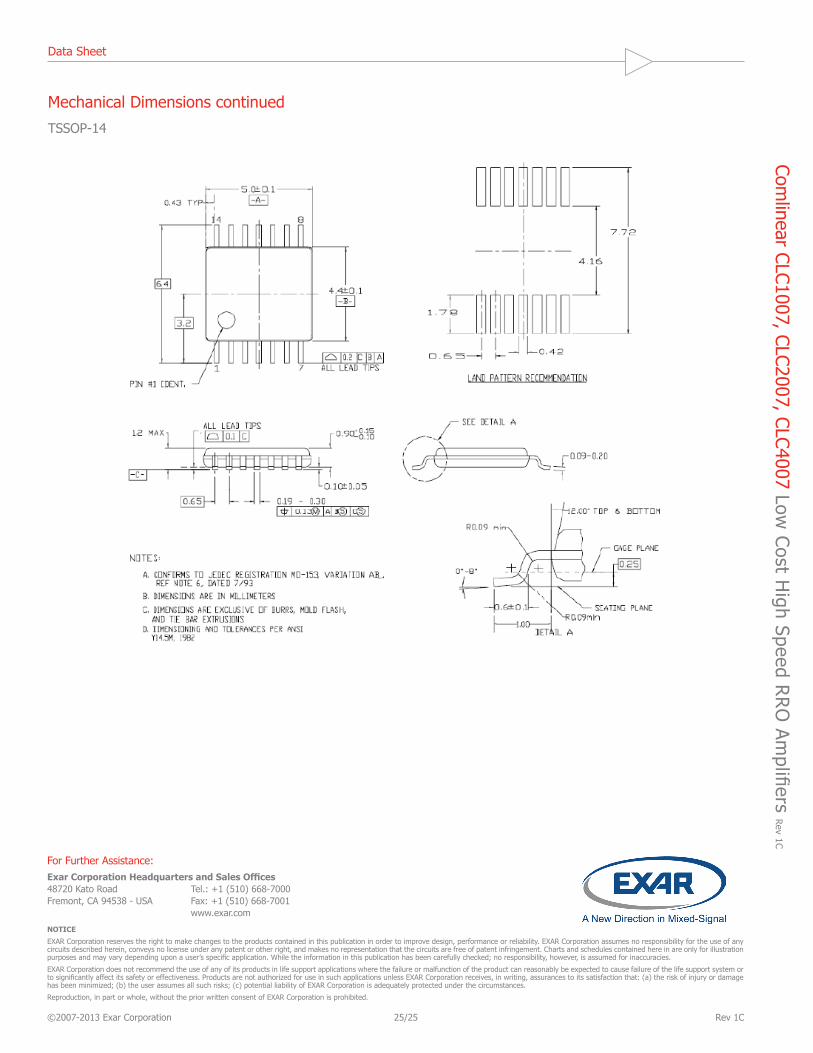
Mechanical Dimensions continued
TSSOP-14