Embed Size (px)
Citation preview

June 2008 Rev 8 1/15
15
ST26C31B
CMOS quad 3-state differential line driver
Features■ TTL input compatible
■ Typical propagation delay: 6 ns
■ Typical output skew: 0.5 ns
■ Output will not load line when VCC = 0 V
■ Meets the requirements of EIA standard RS-422
■ Operation from single 5 V supply
■ 3-state outputs for connection to system buses
■ Low quiescent current
■ Available in surface mount
DescriptionThe ST26C31B is a quad differential line driver designed for digital data transmission over balanced lines and meets all the requirements of EIA standard RS-422 while retaining the low power characteristics of CMOS.
The ST26C31B accepts TTL or CMOS input levels and translates these to RS-422 output levels. This part uses special outputs circuitry common to all four drivers. All outputs are protected against damage due to electrostatic discharge by diode to VCC and ground.
DIP-16 SO-16
TSSOP16
Table 1. Device summary
Order codes Temperature range Package Packaging
ST26C31BN -40 to 85 °C DIP-16 25 parts per tube / 40 tube per box
ST26C31BDR -40 to 85 °C SO-16 (tape and reel) 2500 parts per reel
ST26C31BTR -40 to 85 °C TSSOP16 (tape and reel) 2500 parts per reel
www.st.com

Contents ST26C31B
2/15
Contents
1 Pin configuration . . . . . . . . . . . . . . . . . . . . . . . . . . . . . . . . . . . . . . . . . . . 3
2 Maximum ratings . . . . . . . . . . . . . . . . . . . . . . . . . . . . . . . . . . . . . . . . . . . . 5
3 Electrical characteristics . . . . . . . . . . . . . . . . . . . . . . . . . . . . . . . . . . . . . 6
4 Package mechanical data . . . . . . . . . . . . . . . . . . . . . . . . . . . . . . . . . . . . . 8
5 Revision history . . . . . . . . . . . . . . . . . . . . . . . . . . . . . . . . . . . . . . . . . . . 14
ST26C31B Pin configuration
3/15
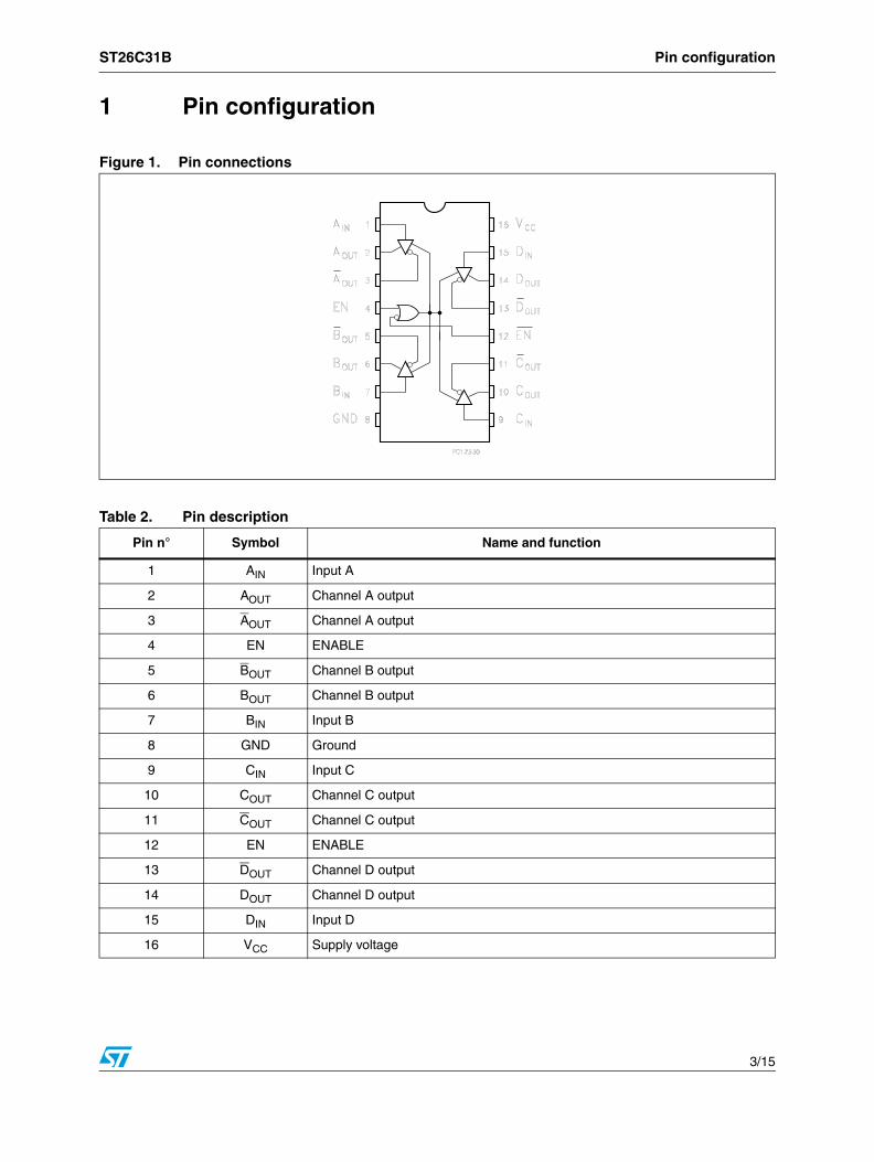
1 Pin configuration
Figure 1. Pin connections
Table 2. Pin description
Pin n° Symbol Name and function
1 AIN Input A
2 AOUT Channel A output
3 AOUT Channel A output
4 EN ENABLE
5 BOUT Channel B output
6 BOUT Channel B output
7 BIN Input B
8 GND Ground
9 CIN Input C
10 COUT Channel C output
11 COUT Channel C output
12 EN ENABLE
13 DOUT Channel D output
14 DOUT Channel D output
15 DIN Input D
16 VCC Supply voltage
Pin configuration ST26C31B
4/15
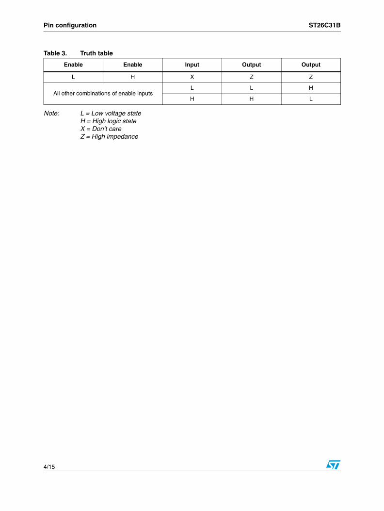
Note: L = Low voltage stateH = High logic stateX = Don’t careZ = High impedance
Table 3. Truth table
Enable Enable Input Output Output
L H X Z Z
All other combinations of enable inputsL L H
H H L
ST26C31B Maximum ratings
5/15
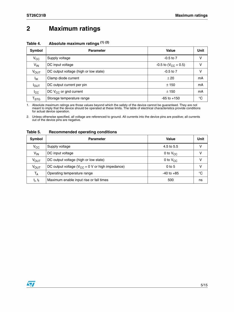
2 Maximum ratings
Table 4. Absolute maximum ratings (1) (2)
1. Absolute maximum ratings are those values beyond which the safety of the device cannot be guaranteed. They are not meant to imply that the device should be operated at these limits. The table of electrical characteristics provide conditions for actual device operation.
2. Unless otherwise specified, all voltage are referenced to ground. All currents into the device pins are positive; all currents out of the device pins are negative.
Symbol Parameter Value Unit
VCC Supply voltage -0.5 to 7 V
VIN DC input voltage -0.5 to (VCC + 0.5) V
VOUT DC output voltage (high or low state) -0.5 to 7 V
IIK Clamp diode current ± 20 mA
IOUT DC output current per pin ± 150 mA
ICC DC VCC or gnd current ± 150 mA
TSTG Storage temperature range -65 to +150 °C
Table 5. Recommended operating conditions
Symbol Parameter Value Unit
VCC Supply voltage 4.5 to 5.5 V
VIN DC input voltage 0 to VCC V
VOUT DC output voltage (high or low state) 0 to VCC V
VOUT DC output voltage (VCC = 0 V or high impedance) 0 to 5 V
TA Operating temperature range -40 to +85 °C
tr, tf Maximum enable input rise or fall times 500 ns

Electrical characteristics ST26C31B
6/15
3 Electrical characteristics
Table 6. Electrical characteristics (VCC = 5 V ± 10 %, unless otherwise specified (1))
1. Unless otherwise specified, min./max. limits apply across the recommended operating temperature range. All typical are given for VCC = 5 V and TA = 25 °C
Symbol Parameter Test conditionsValue
UnitMin. Typ. Max.
VIH High level input voltage 2 V
VIL Low level input voltage 0.8 V
VOH High level output voltage VIN = VIH or VIL, IOUT = -20mA 2.5 3.4 V
VOL Low level output voltage VIN = VIH or VIL, IOUT = +20mA 0.3 0.5 V
VT Differential output voltage RL = 100 Ω (2)
2. See EIA Specification RS422 for exact test conditions.
2 3.1 V
VT-VTDifference in differential output voltage
RL = 100 Ω (2) 0.4 V
VOSCommon mode output voltage
RL = 100 Ω (2) 1.8 3 V
VOS-VOS
Difference in common mode output voltage
RL = 100 Ω (2) 0.4 V
IIN Input current VIN = VCC, GND, VIH or VIL ±1 µA
ICCQuiescent supply current (2) IOUT = 0 µA
VIN = VCC or GND 200 500 µA
VIN = 2.4 or 0.5 V (3)
3. Measured per pin input. All other input at VCC or GND.
0.8 2 mA
IOZ3-state output leakage current
VOUT = VCC or GNDENABLE = VIL ENABLE = VIH
±0.5 ±5 µA
ISCOutput short circuit current
VIN = VCC or GND(2) (4)
4. This is the current sourced when a high output is shorted to ground. Only one output at time should be shorted.
-30 -150 mA
IOFFPower off output leakage current (2) VCC = 0 V
VOUT = 6 V 100 µA
VOUT = -0.25 V -100 µA
ST26C31B Electrical characteristics
7/15
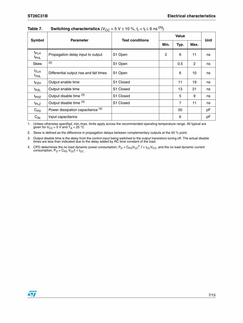
Table 7. Switching characteristics (VCC = 5 V ± 10 %, tr = tf ≤ 6 ns (1))
Symbol Parameter Test conditionsValue
UnitMin. Typ. Max.
tPLHtPHL
Propagation delay input to output S1 Open 2 6 11 ns
Skew (2) S1 Open 0.5 2 ns
tTLHtTHL
Differential output rise and fall times S1 Open 6 10 ns
tPZH Output enable time S1 Closed 11 19 ns
tPZL Output enable time S1 Closed 13 21 ns
tPHZ Output disable time (3) S1 Closed 5 9 ns
tPLZ Output disable time (3) S1 Closed 7 11 ns
CPD Power dissipation capacitance (4) 50 pF
CIN Input capacitance 6 pF
1. Unless otherwise specified, min./max. limits apply across the recommended operating temperature range. All typical are given for VCC = 5 V and TA = 25 °C
2. Skew is defined as the difference in propagation delays between complementary outputs at the 50 % point.
3. Output disable time is the delay from the control input being switched to the output transistors tuning off. The actual disable times are less than indicated due to the delay added by RC time constant of the load.
4. CPD determines the no load dynamic power consumption, PD = CPDVCC2
, f = ICCVCC, and the no load dynamic current consumption, PD = CPD VCCf + ICC .
Package mechanical data ST26C31B
8/15
4 Package mechanical data
In order to meet environmental requirements, ST offers these devices in ECOPACK® packages. These packages have a lead-free second level interconnect. The category of second level interconnect is marked on the package and on the inner box label, in compliance with JEDEC Standard JESD97. The maximum ratings related to soldering conditions are also marked on the inner box label. ECOPACK is an ST trademark. ECOPACK specifications are available at: www.st.com
ST26C31B Package mechanical data
9/15
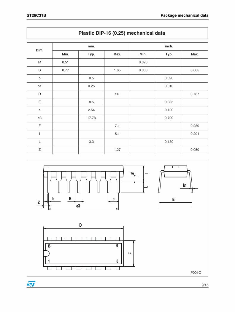
Dim.mm. inch.
Min. Typ. Max. Min. Typ. Max.
a1 0.51 0.020
B 0.77 1.65 0.030 0.065
b 0.5 0.020
b1 0.25 0.010
D 20 0.787
E 8.5 0.335
e 2.54 0.100
e3 17.78 0.700
F 7.1 0.280
I 5.1 0.201
L 3.3 0.130
Z 1.27 0.050
Plastic DIP-16 (0.25) mechanical data
P001C
Package mechanical data ST26C31B
10/15
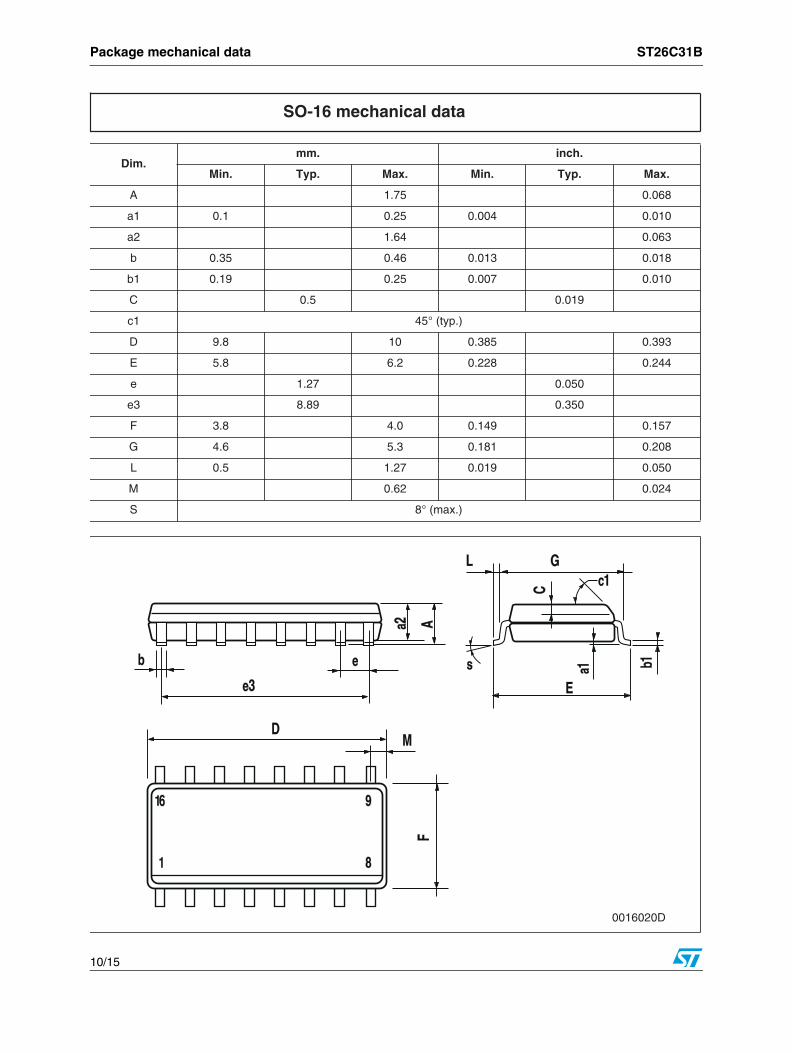
Dim.mm. inch.
Min. Typ. Max. Min. Typ. Max.
A 1.75 0.068
a1 0.1 0.25 0.004 0.010
a2 1.64 0.063
b 0.35 0.46 0.013 0.018
b1 0.19 0.25 0.007 0.010
C 0.5 0.019
c1 45° (typ.)
D 9.8 10 0.385 0.393
E 5.8 6.2 0.228 0.244
e 1.27 0.050
e3 8.89 0.350
F 3.8 4.0 0.149 0.157
G 4.6 5.3 0.181 0.208
L 0.5 1.27 0.019 0.050
M 0.62 0.024
S 8° (max.)
SO-16 mechanical data
0016020D
ST26C31B Package mechanical data
11/15
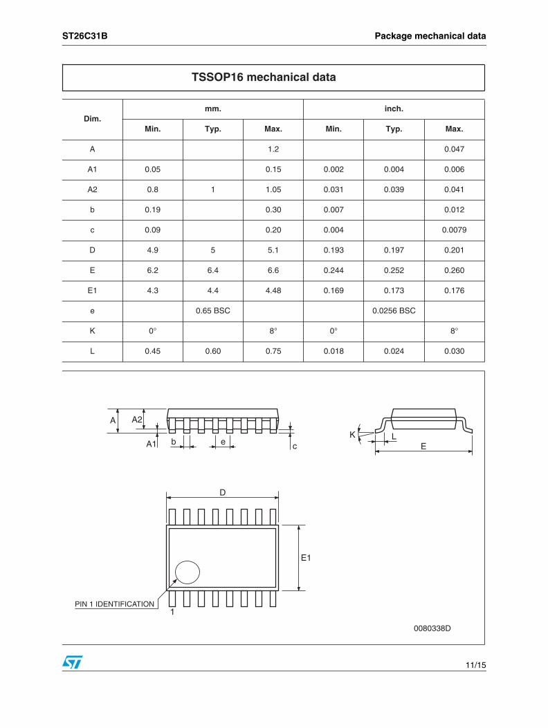
Dim.mm. inch.
Min. Typ. Max. Min. Typ. Max.
A 1.2 0.047
A1 0.05 0.15 0.002 0.004 0.006
A2 0.8 1 1.05 0.031 0.039 0.041
b 0.19 0.30 0.007 0.012
c 0.09 0.20 0.004 0.0079
D 4.9 5 5.1 0.193 0.197 0.201
E 6.2 6.4 6.6 0.244 0.252 0.260
E1 4.3 4.4 4.48 0.169 0.173 0.176
e 0.65 BSC 0.0256 BSC
K 0° 8° 0° 8°
L 0.45 0.60 0.75 0.018 0.024 0.030
TSSOP16 mechanical data
c Eb
A2A
E1
D
1PIN 1 IDENTIFICATION
A1LK
e
0080338D
Package mechanical data ST26C31B
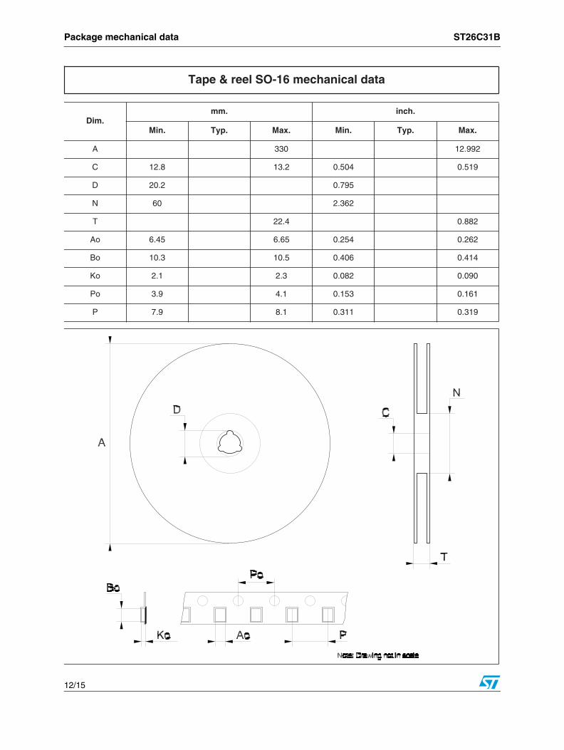
12/15
Dim.mm. inch.
Min. Typ. Max. Min. Typ. Max.
A 330 12.992
C 12.8 13.2 0.504 0.519
D 20.2 0.795
N 60 2.362
T 22.4 0.882
Ao 6.45 6.65 0.254 0.262
Bo 10.3 10.5 0.406 0.414
Ko 2.1 2.3 0.082 0.090
Po 3.9 4.1 0.153 0.161
P 7.9 8.1 0.311 0.319
Tape & reel SO-16 mechanical data
ST26C31B Package mechanical data
13/15
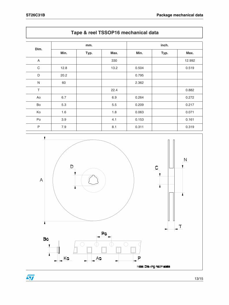
Dim.mm. inch.
Min. Typ. Max. Min. Typ. Max.
A 330 12.992
C 12.8 13.2 0.504 0.519
D 20.2 0.795
N 60 2.362
T 22.4 0.882
Ao 6.7 6.9 0.264 0.272
Bo 5.3 5.5 0.209 0.217
Ko 1.6 1.8 0.063 0.071
Po 3.9 4.1 0.153 0.161
P 7.9 8.1 0.311 0.319
Tape & reel TSSOP16 mechanical data
Revision history ST26C31B
14/15
5 Revision history
Table 8. Document revision history
Date Revision Changes
02-May-2006 7 Order codes updated.
12-Jun-2008 8 Added: Table 1 on page 1.

ST26C31B
15/15
Please Read Carefully:
Information in this document is provided solely in connection with ST products. STMicroelectronics NV and its subsidiaries (“ST”) reserve theright to make changes, corrections, modifications or improvements, to this document, and the products and services described herein at anytime, without notice.
All ST products are sold pursuant to ST’s terms and conditions of sale.
Purchasers are solely responsible for the choice, selection and use of the ST products and services described herein, and ST assumes noliability whatsoever relating to the choice, selection or use of the ST products and services described herein.
No license, express or implied, by estoppel or otherwise, to any intellectual property rights is granted under this document. If any part of thisdocument refers to any third party products or services it shall not be deemed a license grant by ST for the use of such third party productsor services, or any intellectual property contained therein or considered as a warranty covering the use in any manner whatsoever of suchthird party products or services or any intellectual property contained therein.
UNLESS OTHERWISE SET FORTH IN ST’S TERMS AND CONDITIONS OF SALE ST DISCLAIMS ANY EXPRESS OR IMPLIEDWARRANTY WITH RESPECT TO THE USE AND/OR SALE OF ST PRODUCTS INCLUDING WITHOUT LIMITATION IMPLIEDWARRANTIES OF MERCHANTABILITY, FITNESS FOR A PARTICULAR PURPOSE (AND THEIR EQUIVALENTS UNDER THE LAWSOF ANY JURISDICTION), OR INFRINGEMENT OF ANY PATENT, COPYRIGHT OR OTHER INTELLECTUAL PROPERTY RIGHT.
UNLESS EXPRESSLY APPROVED IN WRITING BY AN AUTHORIZED ST REPRESENTATIVE, ST PRODUCTS ARE NOTRECOMMENDED, AUTHORIZED OR WARRANTED FOR USE IN MILITARY, AIR CRAFT, SPACE, LIFE SAVING, OR LIFE SUSTAININGAPPLICATIONS, NOR IN PRODUCTS OR SYSTEMS WHERE FAILURE OR MALFUNCTION MAY RESULT IN PERSONAL INJURY,DEATH, OR SEVERE PROPERTY OR ENVIRONMENTAL DAMAGE. ST PRODUCTS WHICH ARE NOT SPECIFIED AS "AUTOMOTIVEGRADE" MAY ONLY BE USED IN AUTOMOTIVE APPLICATIONS AT USER’S OWN RISK.
Resale of ST products with provisions different from the statements and/or technical features set forth in this document shall immediately voidany warranty granted by ST for the ST product or service described herein and shall not create or extend in any manner whatsoever, anyliability of ST.
ST and the ST logo are trademarks or registered trademarks of ST in various countries.
Information in this document supersedes and replaces all information previously supplied.
The ST logo is a registered trademark of STMicroelectronics. All other names are the property of their respective owners.
© 2008 STMicroelectronics - All rights reserved
STMicroelectronics group of companies
Australia - Belgium - Brazil - Canada - China - Czech Republic - Finland - France - Germany - Hong Kong - India - Israel - Italy - Japan - Malaysia - Malta - Morocco - Singapore - Spain - Sweden - Switzerland - United Kingdom - United States of America
www.st.com