Embed Size (px)
Citation preview
Berkeley Wireless Research Center
Oakland-Eastbay Comsoc
CMOS for Ultra Wideband and 60 GHz Communications
Bob BrodersenBob BrodersenDept. of EECSDept. of EECSUniv. of Calif.Univ. of Calif.
Berkeley Berkeley
http://bwrc.eecs.berkeley.edu
Berkeley Wireless Research Center
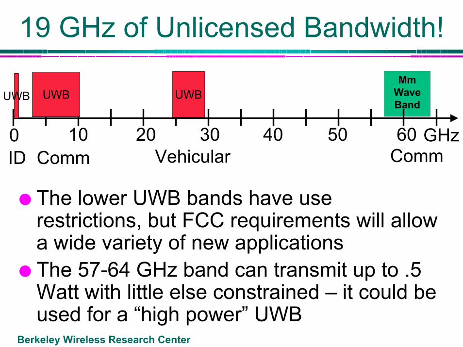
19 GHz of Unlicensed Bandwidth!
The lower UWB bands have use restrictions, but FCC requirements will allow a wide variety of new applicationsThe 57-64 GHz band can transmit up to .5 Watt with little else constrained – it could be used for a “high power” UWB
MmWaveBand
60 GHzComm
20 30Vehicular
UWB UWBUWB
10Comm
40 500ID
Berkeley Wireless Research Center
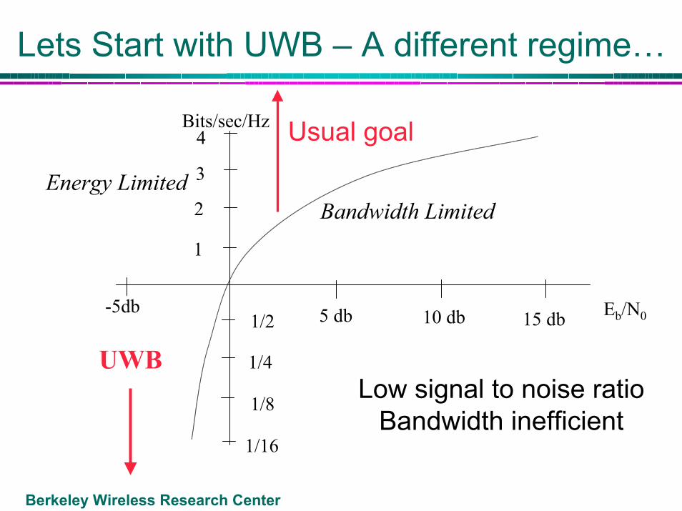
Lets Start with UWB – A different regime…
5 db 10 db 15 db
Bandwidth Limited
Usual goal
Low signal to noise ratioBandwidth inefficient
-5db
1
2
3
4
1/2
1/4
1/8
1/16
Bits/sec/Hz
Energy Limited
UWB
Eb/N0
Berkeley Wireless Research Center
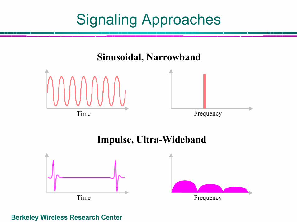
Signaling Approaches
Sinusoidal, Narrowband
Frequency
Time
Time
Frequency
Impulse, Ultra-Wideband
Berkeley Wireless Research Center
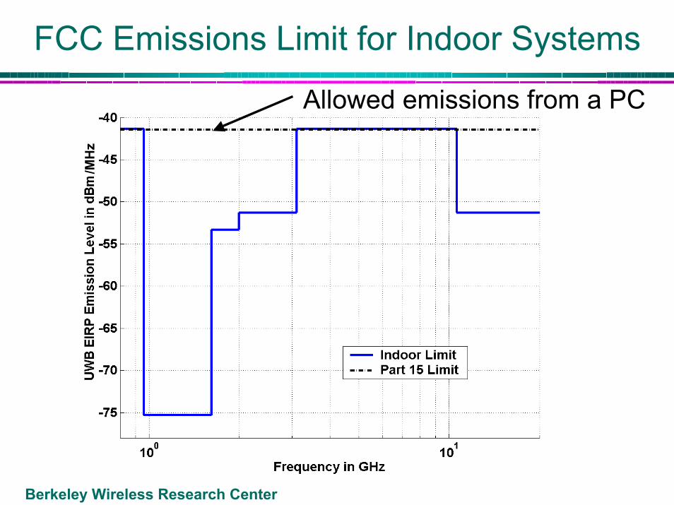
FCC Emissions Limit for Indoor Systems
Allowed emissions from a PC/M
Hz
Berkeley Wireless Research Center
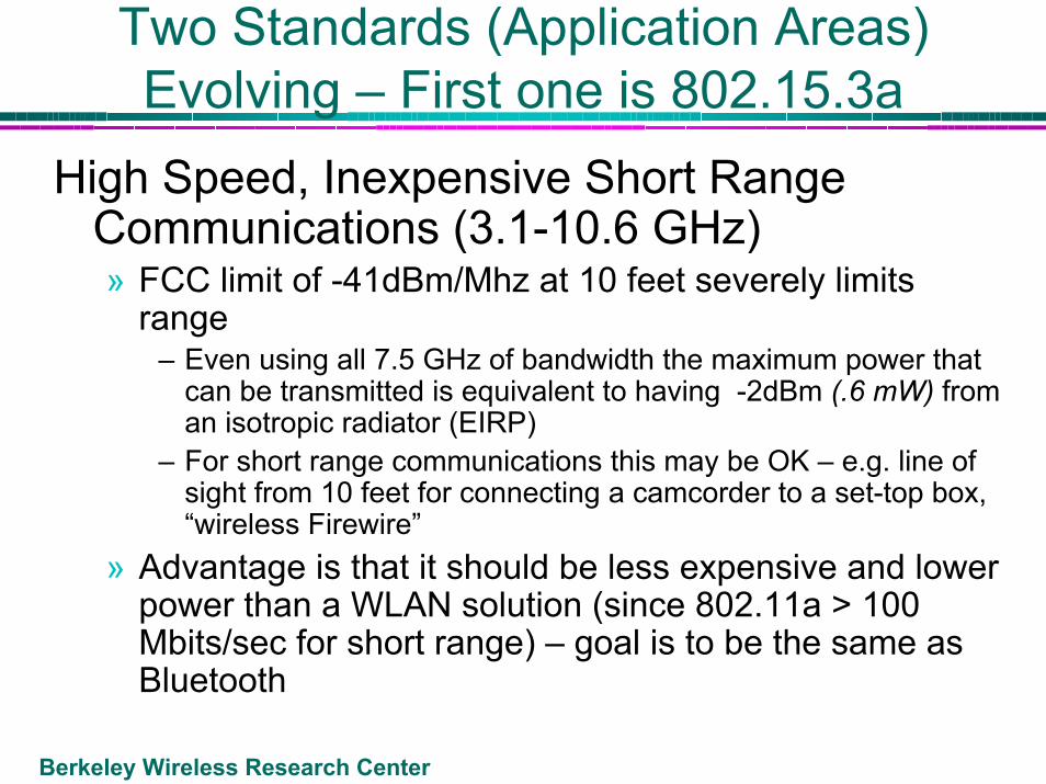
Two Standards (Application Areas) Evolving – First one is 802.15.3a
High Speed, Inexpensive Short Range Communications (3.1-10.6 GHz)» FCC limit of -41dBm/Mhz at 10 feet severely limits
range – Even using all 7.5 GHz of bandwidth the maximum power that
can be transmitted is equivalent to having -2dBm (.6 mW) from an isotropic radiator (EIRP)
– For short range communications this may be OK – e.g. line of sight from 10 feet for connecting a camcorder to a set-top box, “wireless Firewire”
» Advantage is that it should be less expensive and lower power than a WLAN solution (since 802.11a > 100 Mbits/sec for short range) – goal is to be the same as Bluetooth
Berkeley Wireless Research Center
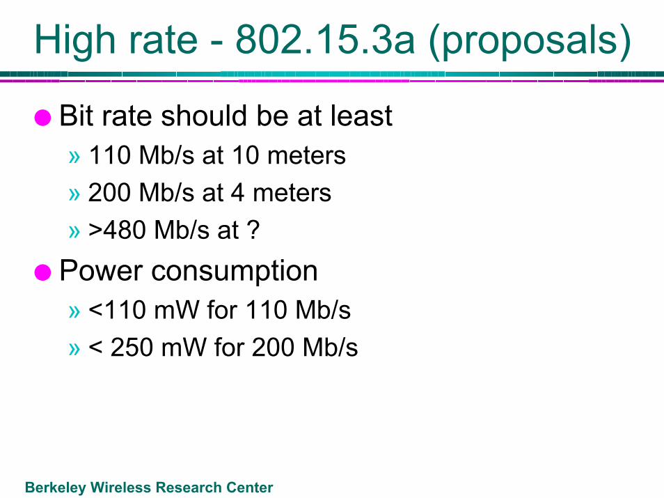
High rate - 802.15.3a (proposals)
Bit rate should be at least » 110 Mb/s at 10 meters» 200 Mb/s at 4 meters» >480 Mb/s at ?
Power consumption » <110 mW for 110 Mb/s» < 250 mW for 200 Mb/s
Berkeley Wireless Research Center
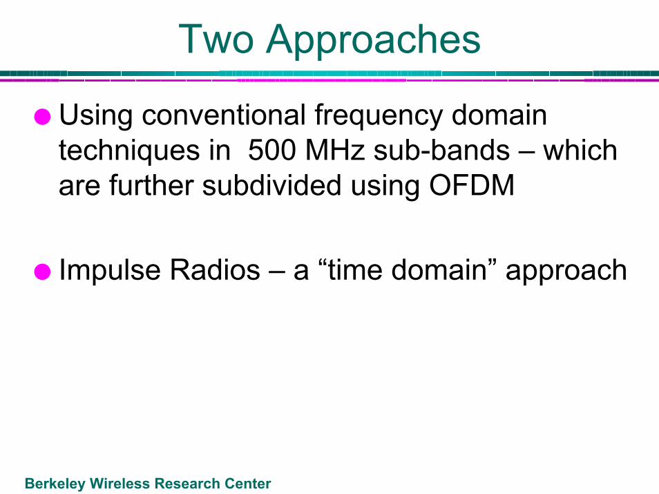
Two Approaches
Using conventional frequency domain techniques in 500 MHz sub-bands – which are further subdivided using OFDM
Impulse Radios – a “time domain” approach
Berkeley Wireless Research Center
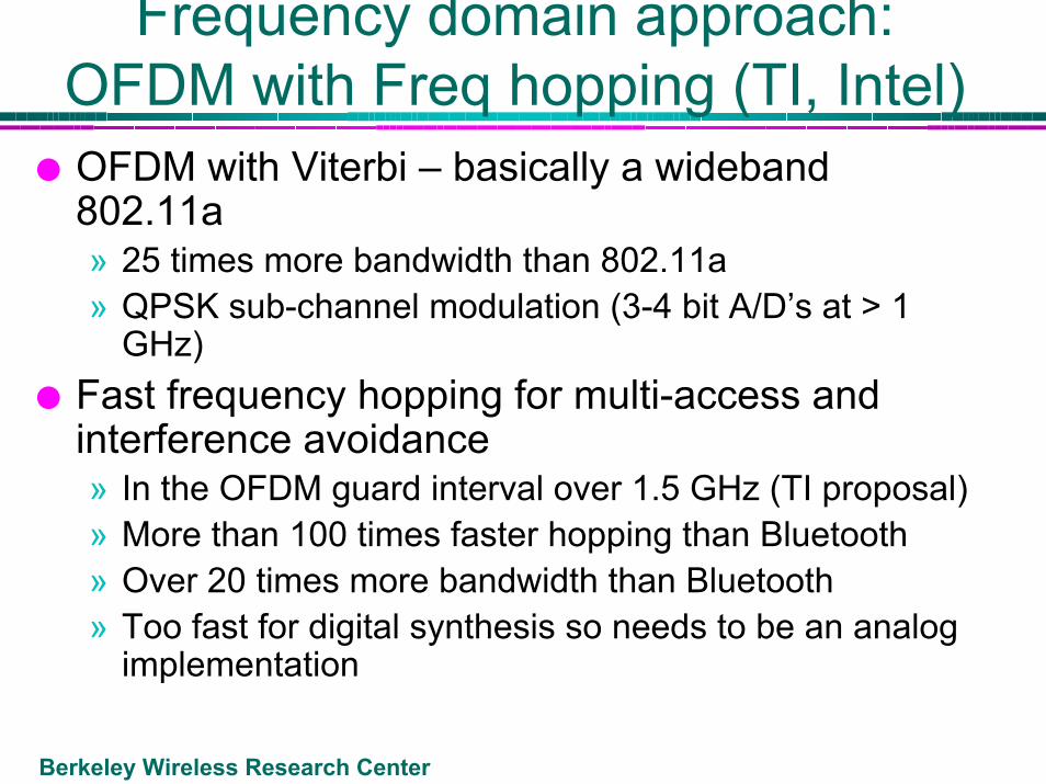
Frequency domain approach:OFDM with Freq hopping (TI, Intel)OFDM with Viterbi – basically a wideband 802.11a» 25 times more bandwidth than 802.11a» QPSK sub-channel modulation (3-4 bit A/D’s at > 1
GHz)Fast frequency hopping for multi-access and interference avoidance» In the OFDM guard interval over 1.5 GHz (TI proposal)» More than 100 times faster hopping than Bluetooth» Over 20 times more bandwidth than Bluetooth» Too fast for digital synthesis so needs to be an analog
implementation
Berkeley Wireless Research Center
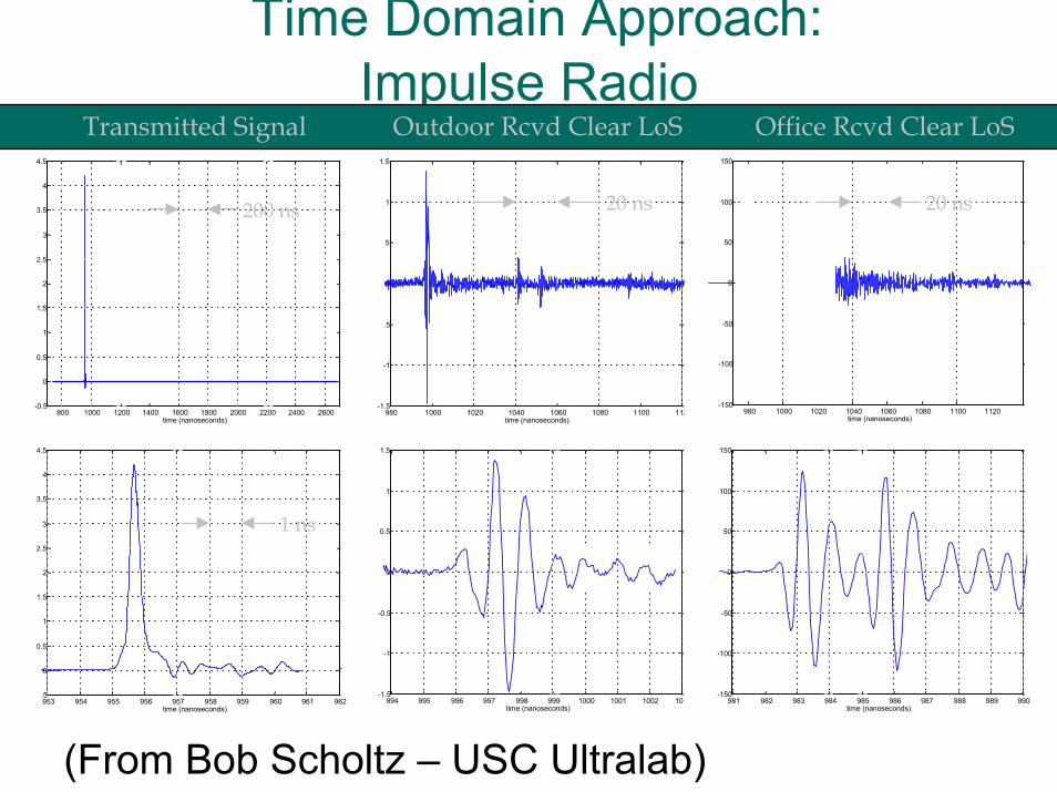
Time Domain Approach:Impulse Radio
-0.5
0.5
1
1.5
2
2.5
3
3.5
4.5
980 1000 1020 1040 1060 1080 1100 1120-1.5
-1
-0.5
0
0.5
1
1.5
time (nanoseconds)
994 995 996 997 998 999 1000 1001 1002 1003-1.5
-1
-0.5
0
0.5
1
1.5
time (nanoseconds)
980 1000 1020 1040 1060 1080 1100 1120-150
-100
-50
50
100
150
time (nanoseconds)
981 982 983 984 985 986 987 988 989 990-150
-100
-5
0
50
100
150
time (nanoseconds)
Transmitted Signal Outdoor Rcvd Clear LoS Office Rcvd Clear LoS
200 ns 20 ns
800 1000 1200 1400 1600 1800 2000 2200 2400 2600time (nanoseconds)
953 954 955 956 957 958 959 960 961 962-0.5
0.5
1.5
2.5
3.5
4.5
time (nanoseconds)
1 ns
(From Bob Scholtz – USC Ultralab)
0
4
0
1
2
3
4
0
20 ns
0
Berkeley Wireless Research Center
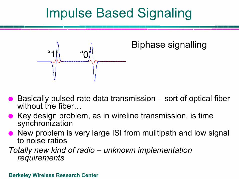
Impulse Based Signaling
Biphase signalling“1” “0”
Basically pulsed rate data transmission – sort of optical fiber without the fiber…Key design problem, as in wireline transmission, is time synchronizationNew problem is very large ISI from muiltipath and low signal to noise ratios
Totally new kind of radio – unknown implementation requirements
Berkeley Wireless Research Center
Observation
Most probable strategy for UWB to make an impact in high rate at much lower power and cost than existing techniques is to use a pulse based approach
Hard to understand that by scaling up conventional techniques by an order of magnitude that power and cost will reduce by an order of magnitude???
Berkeley Wireless Research Center
Second Application Area – 802.15.4a
Low Data Rate, Short Range Communications with Locationing (< 960 MHz)» Round trip time for pulse provides range
information – multiple range estimates provides location
» Used for asset tracking – a sophisticated RFID tag that provides location
» Can be used to track people (children, firemen in buildings)
» Sensor networks
Berkeley Wireless Research Center
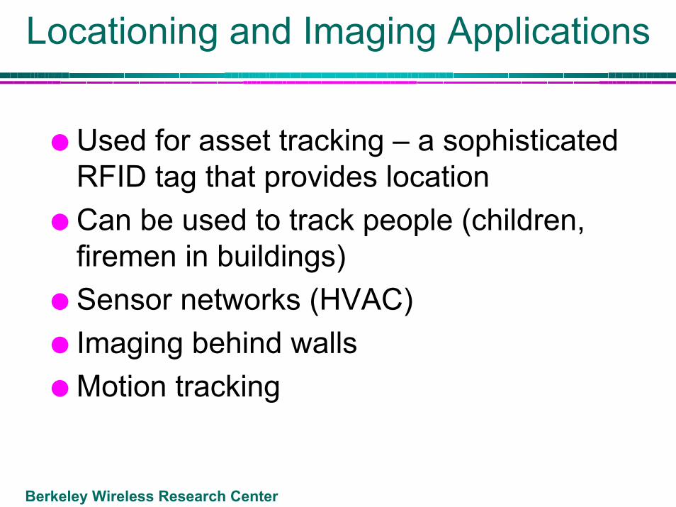
Locationing and Imaging Applications
Used for asset tracking – a sophisticated RFID tag that provides locationCan be used to track people (children, firemen in buildings)Sensor networks (HVAC)Imaging behind wallsMotion tracking
Berkeley Wireless Research Center
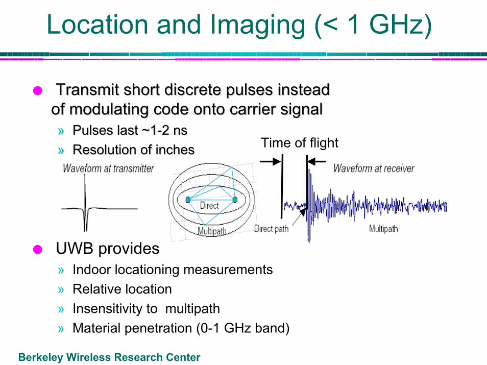
Location and Imaging (< 1 GHz)
UWB provides» Indoor locationing measurements» Relative location » Insensitivity to multipath» Material penetration (0-1 GHz band)
Time of flight
Transmit short discrete pulses instead Transmit short discrete pulses instead of modulating code onto carrier signalof modulating code onto carrier signal»» Pulses last ~1Pulses last ~1--2 ns2 ns»» Resolution of inches Resolution of inches
Berkeley Wireless Research Center
Locationing and Imaging (< 1GHz)
Advantages» Unique capability of UWB» Mostly digital implementation with low
performance analog» Standards not as critical
Disadvantages» Markets not defined (but Microsoft has defined a
standard and 802.15.4a is starting up)» Unknown architectures
Berkeley Wireless Research Center
For UWB to be Disruptive
Exploit locationing and imaging capability
OrHigh rate communications using a
digital pulse based system
Berkeley Wireless Research Center
What about the IEEE/industry standards process?
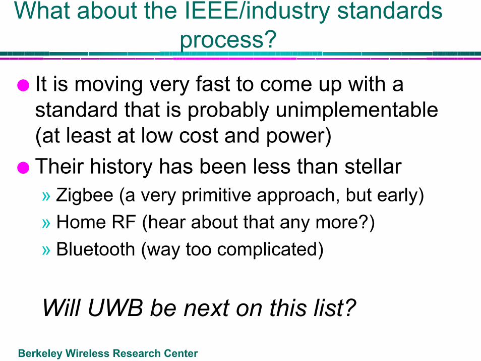
It is moving very fast to come up with a standard that is probably unimplementable(at least at low cost and power)Their history has been less than stellar» Zigbee (a very primitive approach, but early)» Home RF (hear about that any more?)» Bluetooth (way too complicated)
Will UWB be next on this list?
Berkeley Wireless Research Center
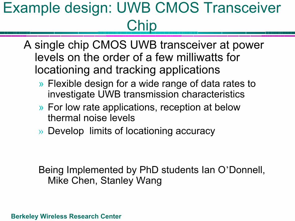
Example design: UWB CMOS Transceiver Chip
A single chip CMOS UWB transceiver at power levels on the order of a few milliwatts for locationing and tracking applications » Flexible design for a wide range of data rates to
investigate UWB transmission characteristics» For low rate applications, reception at below
thermal noise levels» Develop limits of locationing accuracy
Being Implemented by PhD students Ian O’Donnell, Mike Chen, Stanley Wang
Berkeley Wireless Research Center
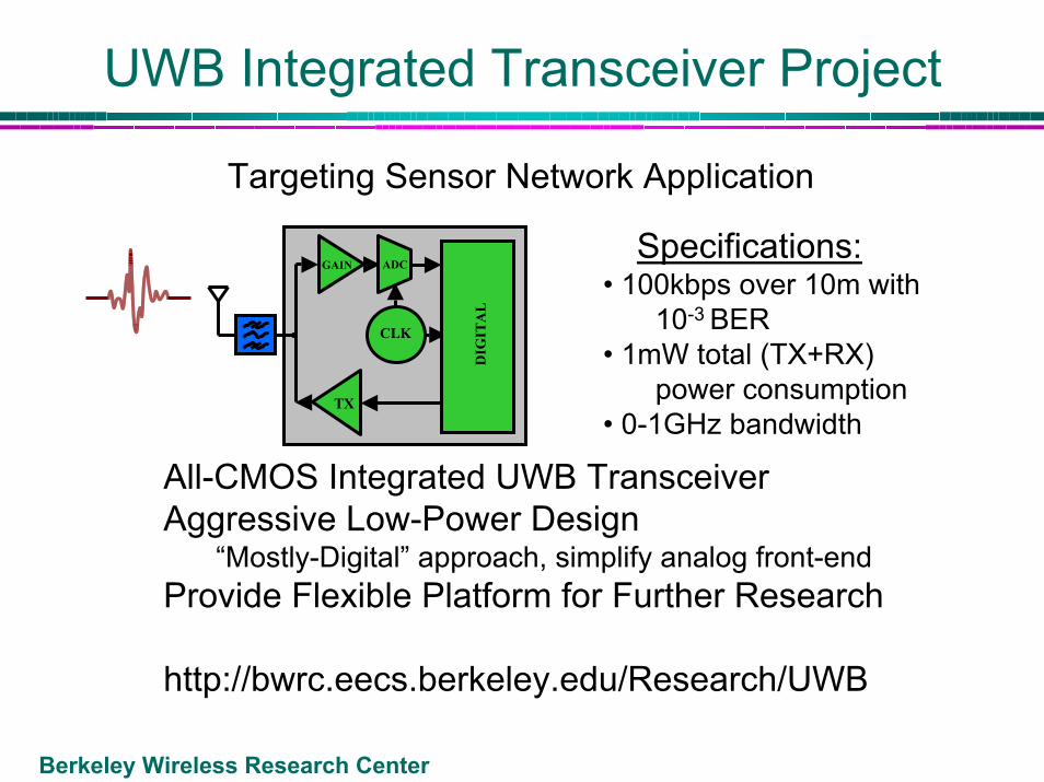
UWB Integrated Transceiver Project
Targeting Sensor Network Application
Specifications:• 100kbps over 10m with
10-3 BER • 1mW total (TX+RX)
power consumption• 0-1GHz bandwidth
GAIN
TX
CLK
ADC
DIG
ITA
LAll-CMOS Integrated UWB TransceiverAggressive Low-Power Design
“Mostly-Digital” approach, simplify analog front-endProvide Flexible Platform for Further Research
http://bwrc.eecs.berkeley.edu/Research/UWB
Berkeley Wireless Research Center
CMOS Analog Frontend
Berkeley Wireless Research Center
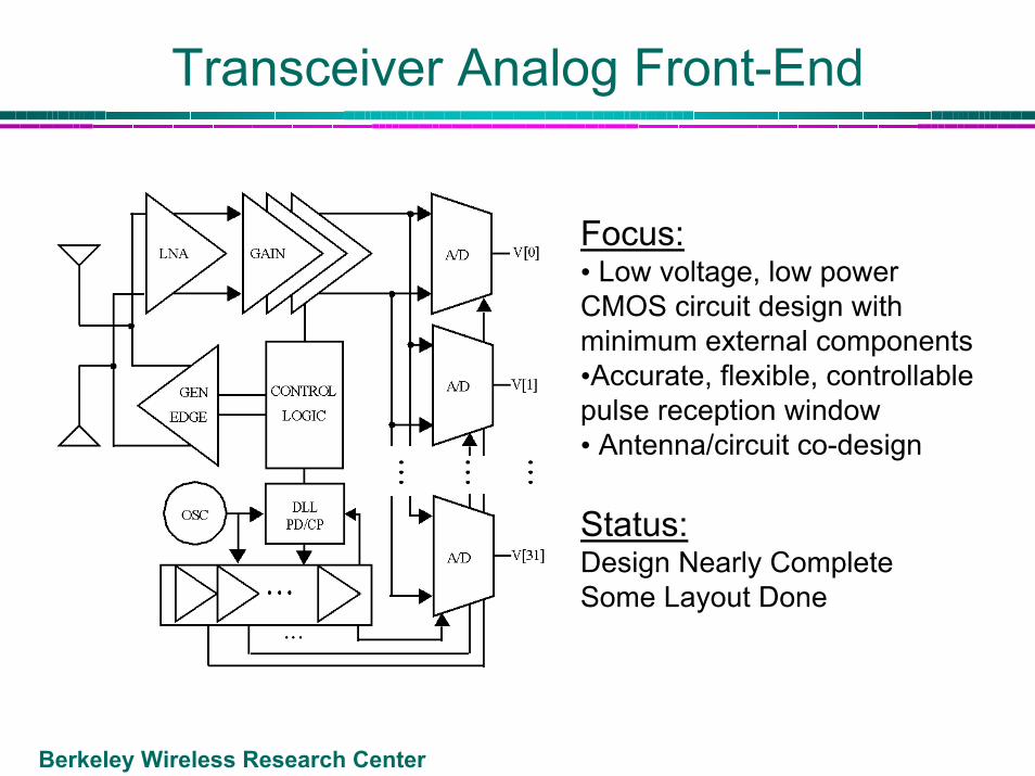
Transceiver Analog Front-End
Focus: • Low voltage, low power CMOS circuit design with minimum external components •Accurate, flexible, controllable pulse reception window• Antenna/circuit co-design
Status:Design Nearly CompleteSome Layout Done
Berkeley Wireless Research Center
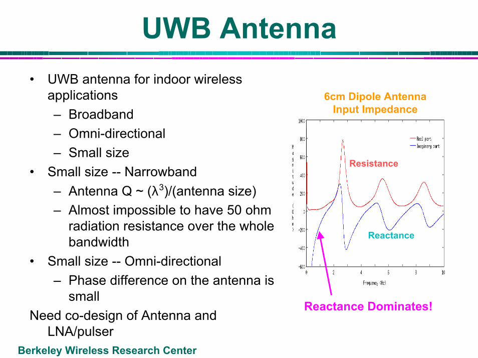
UWB Antenna• UWB antenna for indoor wireless
applications– Broadband– Omni-directional– Small size
• Small size -- Narrowband– Antenna Q ~ (λ3)/(antenna size)– Almost impossible to have 50 ohm
radiation resistance over the whole bandwidth
• Small size -- Omni-directional– Phase difference on the antenna is
small Need co-design of Antenna and
LNA/pulser
6cm Dipole AntennaInput Impedance
Resistance
Reactance
Reactance Dominates!
Berkeley Wireless Research Center
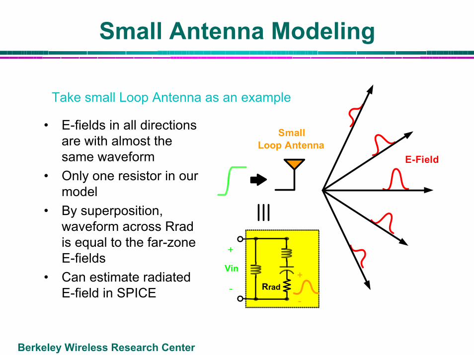
Small Antenna Modeling
• E-fields in all directions are with almost the same waveform
• Only one resistor in our model
• By superposition, waveform across Rradis equal to the far-zone E-fields
• Can estimate radiated E-field in SPICE
Take small Loop Antenna as an example
E-Field
Rrad+
-
Vin
+
-
SmallLoop Antenna
Berkeley Wireless Research Center
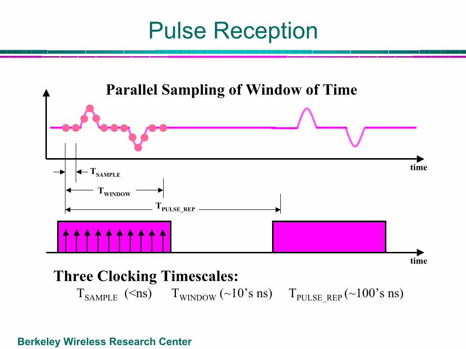
Pulse Reception
Parallel Sampling of Window of Time
timeTSAMPLE
TWINDOW
TPULSE_REP
time
Three Clocking Timescales:TSAMPLE (<ns) TWINDOW (~10’s ns) TPULSE_REP (~100’s ns)
Berkeley Wireless Research Center
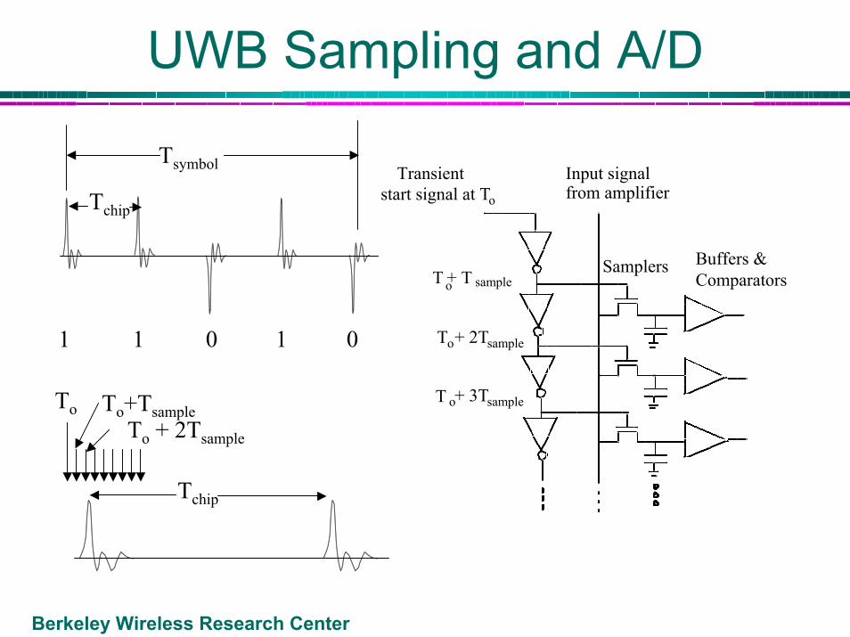
UWB Sampling and A/D
Transientstart signal at To
Input signal from amplifier
Samplers
To+ 2Tsample
T o+ 3Tsample
T o+ T sample
To To+TsampleTo + 2Tsample
Tchip
Tsymbol
Tchip
1 1 0 1 0
Buffers &Comparators
Berkeley Wireless Research Center
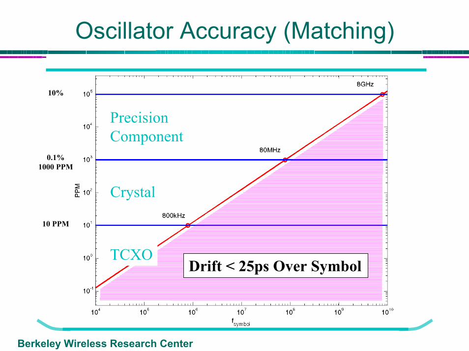
Oscillator Accuracy (Matching)
Drift < 25ps Over Symbol
Crystal
PrecisionComponent
10 PPM
0.1%1000 PPM
10%
TCXO
Berkeley Wireless Research Center
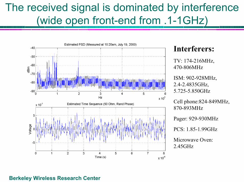
The received signal is dominated by interference (wide open front-end from .1-1GHz)
Interferers:TV: 174-216MHz, 470-806MHz
ISM: 902-928MHz,2.4-2.4835GHz,5.725-5.850GHz
Cell phone:824-849MHz,870-893MHz
Pager: 929-930MHz
PCS: 1.85-1.99GHz
Microwave Oven: 2.45GHz
Berkeley Wireless Research Center
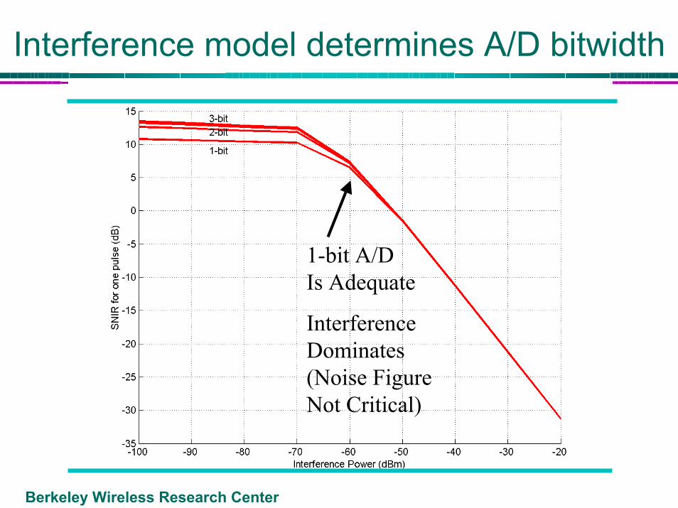
Interference model determines A/D bitwidth
1-bit A/DIs Adequate
Interference Dominates (Noise FigureNot Critical)
Berkeley Wireless Research Center
UWB Receive Baseband
Berkeley Wireless Research Center
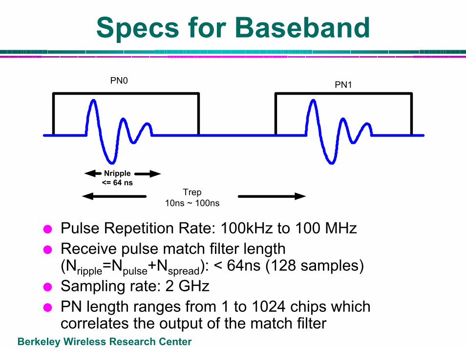
Specs for BasebandPN0 PN1
Nripple<= 64 ns
Trep10ns ~ 100ns
Pulse Repetition Rate: 100kHz to 100 MHzReceive pulse match filter length (Nripple=Npulse+Nspread): < 64ns (128 samples)Sampling rate: 2 GHzPN length ranges from 1 to 1024 chips which correlates the output of the match filter
Berkeley Wireless Research Center
Processing gain – How much is needed?
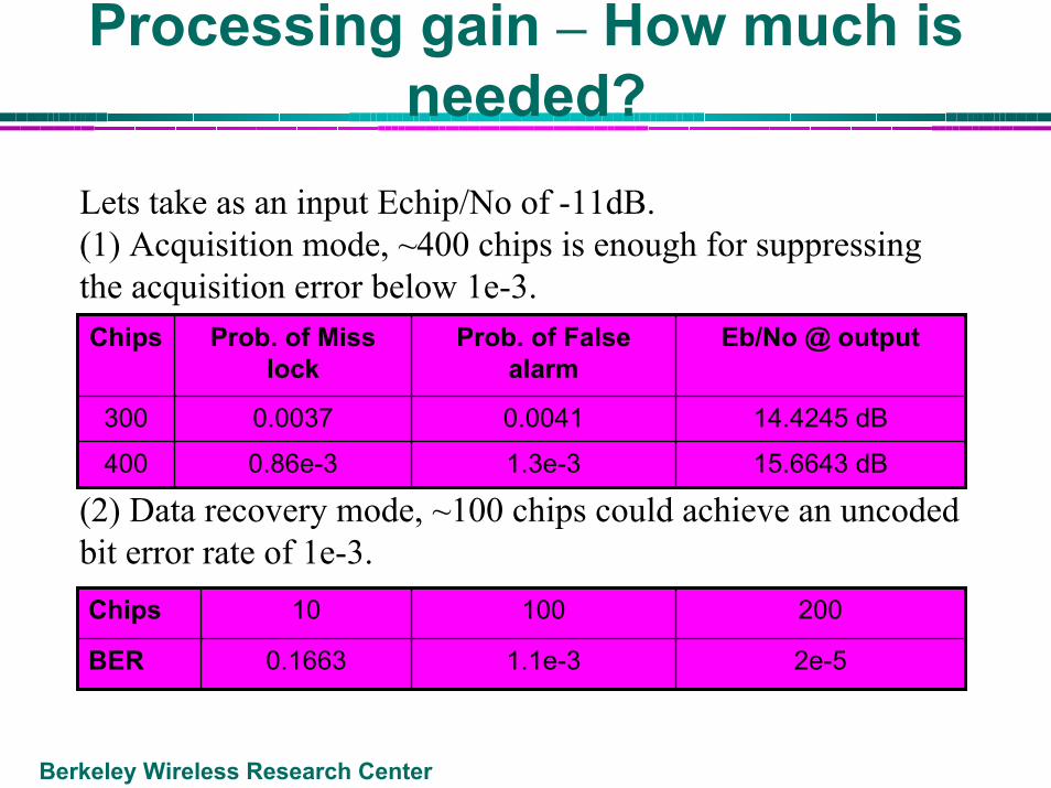
15.6643 dB1.3e-30.86e-3400
14.4245 dB0.00410.0037300
Eb/No @ outputProb. of False alarm
Prob. of Miss lock
Chips
Lets take as an input Echip/No of -11dB. (1) Acquisition mode, ~400 chips is enough for suppressing the acquisition error below 1e-3.
(2) Data recovery mode, ~100 chips could achieve an uncoded bit error rate of 1e-3.
2e-51.1e-30.1663BER
20010010Chips
Berkeley Wireless Research Center
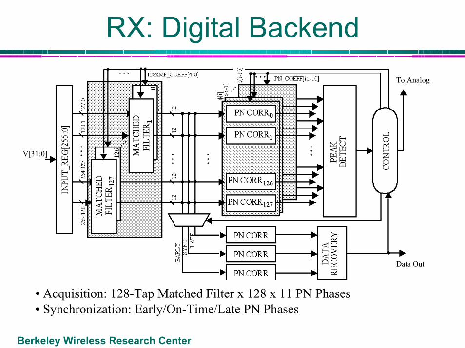
RX: Digital Backend
V[31:0]
To Analog
Data Out
• Acquisition: 128-Tap Matched Filter x 128 x 11 PN Phases• Synchronization: Early/On-Time/Late PN Phases
Berkeley Wireless Research Center
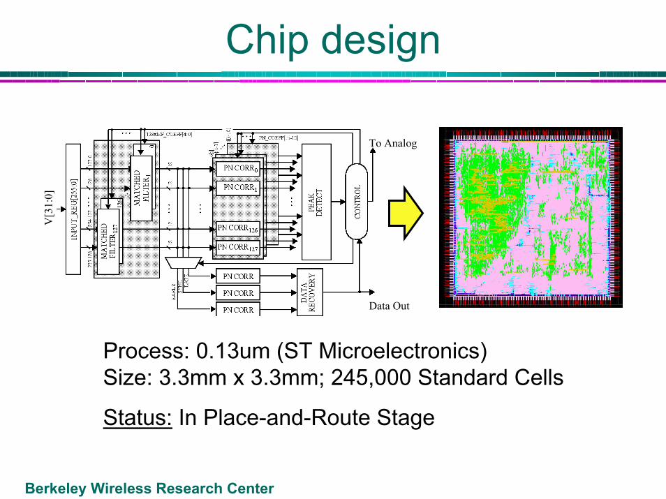
Chip designV
[31:
0]
To Analog
Data Out
Process: 0.13um (ST Microelectronics)Size: 3.3mm x 3.3mm; 245,000 Standard Cells
Status: In Place-and-Route Stage
Berkeley Wireless Research Center
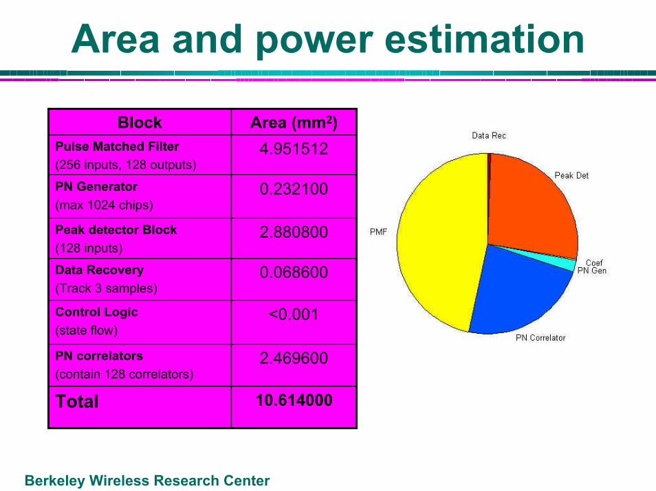
Area and power estimation
2.469600PN correlators(contain 128 correlators)
<0.001Control Logic(state flow)
2.880800Peak detector Block(128 inputs)
0.068600Data Recovery (Track 3 samples)
10.614000Total
0.232100PN Generator (max 1024 chips)
4.951512Pulse Matched Filter (256 inputs, 128 outputs)
Area (mm2)Block
Berkeley Wireless Research Center
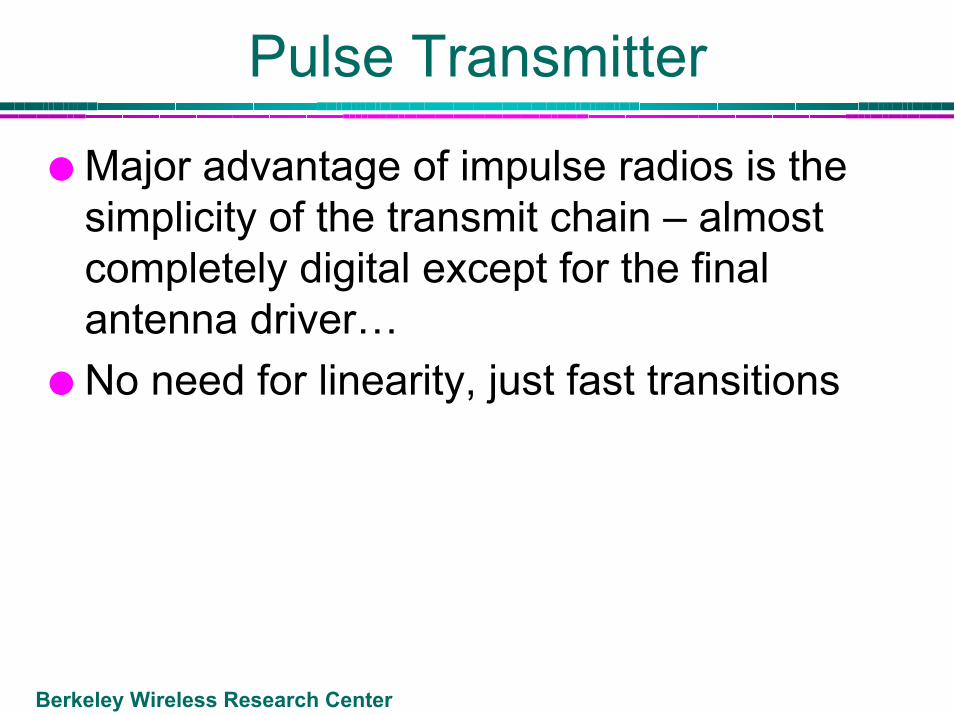
Pulse Transmitter
Major advantage of impulse radios is the simplicity of the transmit chain – almost completely digital except for the final antenna driver…No need for linearity, just fast transitions
Berkeley Wireless Research Center
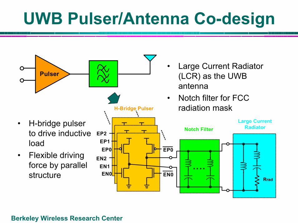
UWB Pulser/Antenna Co-design
• Large Current Radiator (LCR) as the UWB antenna
• Notch filter for FCC radiation mask
EN0 EN0
EP0EP0
EN1EN2
EP1EP2
Large CurrentRadiator
Rrad
Notch Filter
H-Bridge Pulser
Pulser
• H-bridge pulser to drive inductive load
• Flexible driving force by parallel structure
Berkeley Wireless Research Center
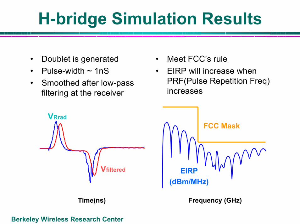
H-bridge Simulation Results
• Doublet is generated• Pulse-width ~ 1nS• Smoothed after low-pass
filtering at the receiver
• Meet FCC’s rule• EIRP will increase when
PRF(Pulse Repetition Freq) increases
EIRP(dBm/MHz)
Frequency (GHz)
FCC MaskVRrad
Vfiltered
Time(ns)
Berkeley Wireless Research Center
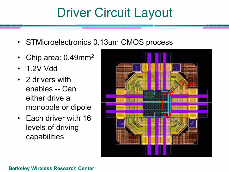
Driver Circuit Layout
• STMicroelectronics 0.13um CMOS process
Driver
• Chip area: 0.49mm2
• 1.2V Vdd• 2 drivers with
enables -- Can either drive a monopole or dipole
• Each driver with 16 levels of driving capabilities
Berkeley Wireless Research Center
Status
Chip tape out by summer in .13 micron technologyStay tuned at http://bwrc.eecs.berkeley.edu/Research/UWB/
Berkeley Wireless Research Center
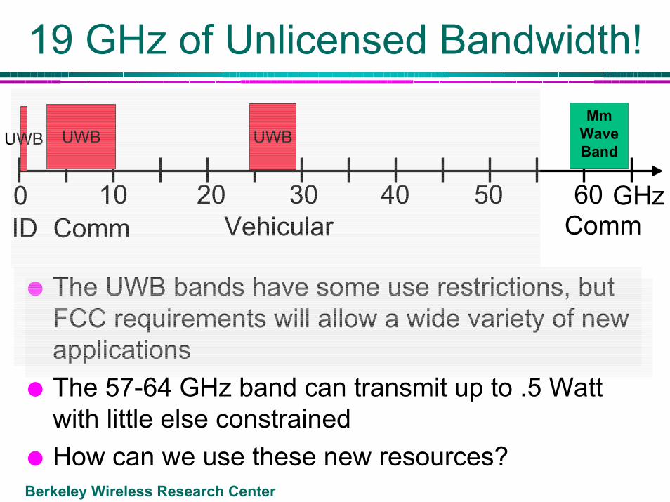
19 GHz of Unlicensed Bandwidth!
The UWB bands have some use restrictions, but FCC requirements will allow a wide variety of new applicationsThe 57-64 GHz band can transmit up to .5 Watt with little else constrainedHow can we use these new resources?
0 10 20
UWBUWB UWBMm
WaveBand
30 40 50 60 GHzComm Vehicular CommID
Berkeley Wireless Research Center
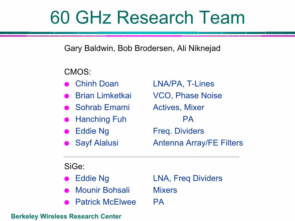
60 GHz Research TeamGary Baldwin, Bob Brodersen, Ali Niknejad
CMOS:Chinh Doan LNA/PA, T-LinesBrian Limketkai VCO, Phase NoiseSohrab Emami Actives, MixerHanching Fuh PAEddie Ng Freq. DividersSayf Alalusi Antenna Array/FE Filters
SiGe:Eddie Ng LNA, Freq DividersMounir Bohsali MixersPatrick McElwee PA
Berkeley Wireless Research Center
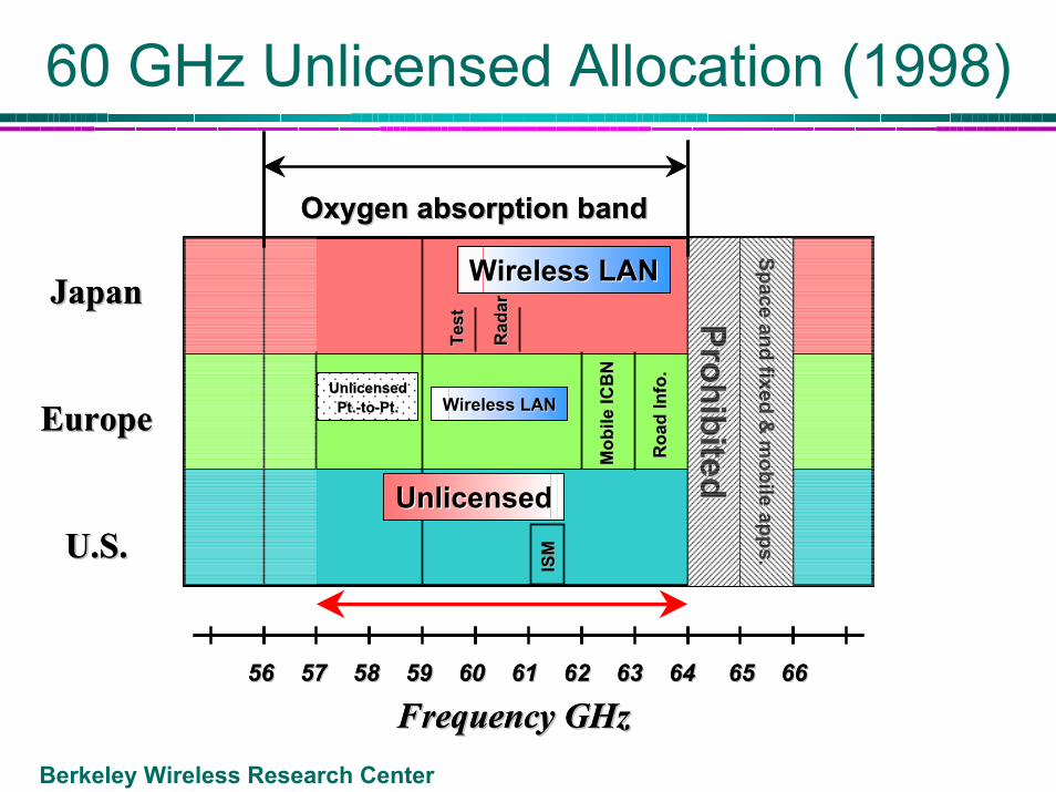
60 GHz Unlicensed Allocation (1998)
ProhibitedProhibited
UnlicensedUnlicensed
Wireless LANWireless LAN
Wireless LANWireless LAN
Test
Test
Rad
arR
adar
Mob
ile IC
BN
Mob
ile IC
BN
Roa
d In
fo.
Roa
d In
fo.
ISM
ISM
UnlicensedUnlicensedPt.Pt.--toto--Pt.Pt.
Space and fixed & m
obile apps.Space and fixed &
mobile apps.
ProhibitedProhibited
UnlicensedUnlicensed
Wireless LANWireless LAN
Wireless LANWireless LAN
Test
Test
Rad
arR
adar
Mob
ile IC
BN
Mob
ile IC
BN
Roa
d In
fo.
Roa
d In
fo.
ISM
ISM
UnlicensedUnlicensedPt.Pt.--toto--Pt.Pt.
Space and fixed & m
obile apps.Space and fixed &
mobile apps.
56 57 58 59 60 61 62 63 64 65 66 56 57 58 59 60 61 62 63 64 65 66
Frequency GHzFrequency GHz
JapanJapan
EuropeEurope
U.S.U.S.
Oxygen absorption bandOxygen absorption bandOxygen absorption bandOxygen absorption band
JapanJapan
EuropeEurope
U.S.U.S.
56 57 58 59 60 61 62 63 64 65 66 56 57 58 59 60 61 62 63 64 65 66
Frequency GHzFrequency GHz
Berkeley Wireless Research Center
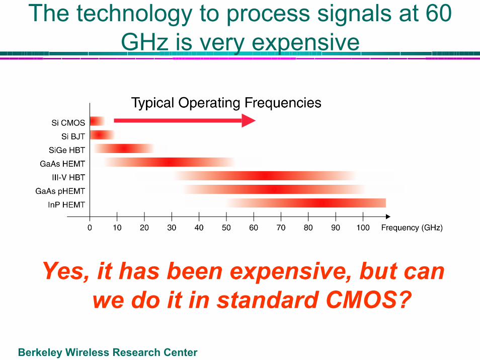
Why Isn’t 60 GHz in Widespread Use?
Oxygen absorbs RF energy at 60 GHz The technology to process signals at 60 GHz is very expensiveThe signal radiated is attenuated by the small antenna size – i.e. the power received at 60 Ghz from a half wave dipole is 20 dB less than at 5GHz.
Berkeley Wireless Research Center
Oxygen attenuation
The oxygen attenuation is about 15 dB/km, so for most of the applications this is not a significant component of loss
For long range outdoor links, worst case rain conditions are actually a bigger issue
Berkeley Wireless Research Center
The technology to process signals at 60 GHz is very expensive
Yes, it has been expensive, but can we do it in standard CMOS?
Berkeley Wireless Research Center
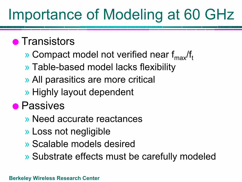
Importance of Modeling at 60 GHz
Transistors» Compact model not verified near fmax/ft» Table-based model lacks flexibility» All parasitics are more critical » Highly layout dependent
Passives» Need accurate reactances» Loss not negligible» Scalable models desired» Substrate effects must be carefully modeled
Berkeley Wireless Research Center
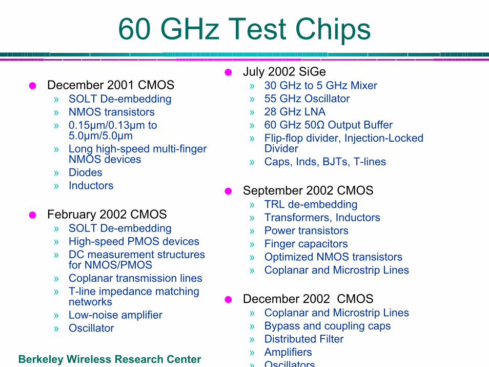
60 GHz Test ChipsDecember 2001 CMOS
» SOLT De-embedding» NMOS transistors» 0.15µm/0.13µm to
5.0µm/5.0µm» Long high-speed multi-finger
NMOS devices» Diodes» Inductors
February 2002 CMOS» SOLT De-embedding» High-speed PMOS devices» DC measurement structures
for NMOS/PMOS» Coplanar transmission lines» T-line impedance matching
networks» Low-noise amplifier» Oscillator
July 2002 SiGe» 30 GHz to 5 GHz Mixer» 55 GHz Oscillator» 28 GHz LNA» 60 GHz 50Ω Output Buffer» Flip-flop divider, Injection-Locked
Divider» Caps, Inds, BJTs, T-lines
September 2002 CMOS» TRL de-embedding» Transformers, Inductors» Power transistors» Finger capacitors» Optimized NMOS transistors» Coplanar and Microstrip Lines
December 2002 CMOS» Coplanar and Microstrip Lines» Bypass and coupling caps» Distributed Filter» Amplifiers» Oscillators
Berkeley Wireless Research Center
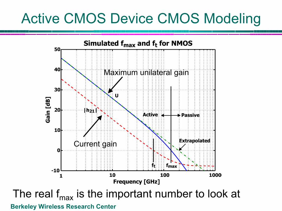
Active CMOS Device CMOS Modeling
Maximum unilateral gain
Current gain
The real fmax is the important number to look at
Berkeley Wireless Research Center
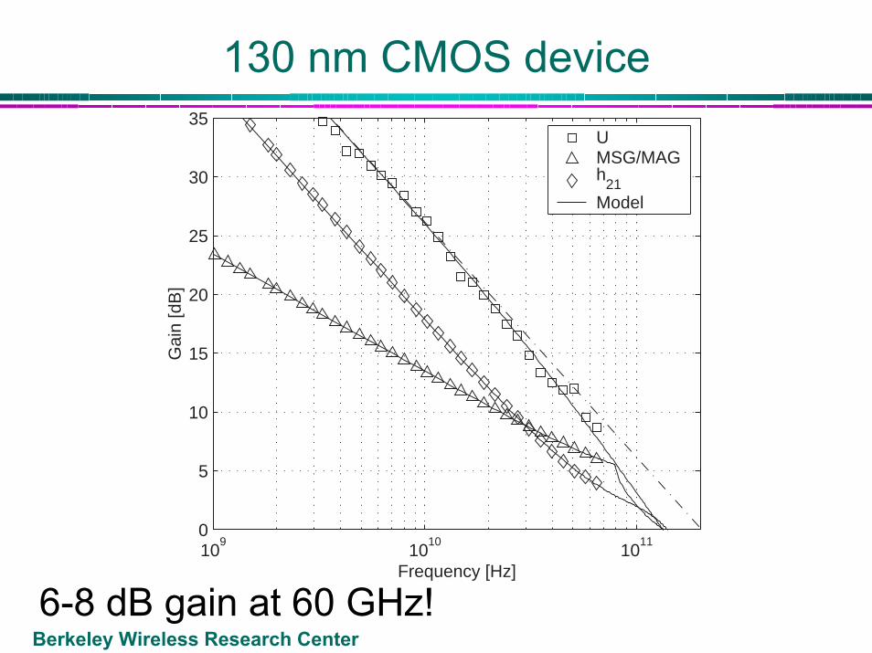
130 nm CMOS device
6-8 dB gain at 60 GHz!
Maximum unilateral gain
Current gain
109
1010
1011
0
5
10
15
20
25
30
35
Frequency [Hz]
Gai
n [d
B]
UMSG/MAGh
21Model
Berkeley Wireless Research Center
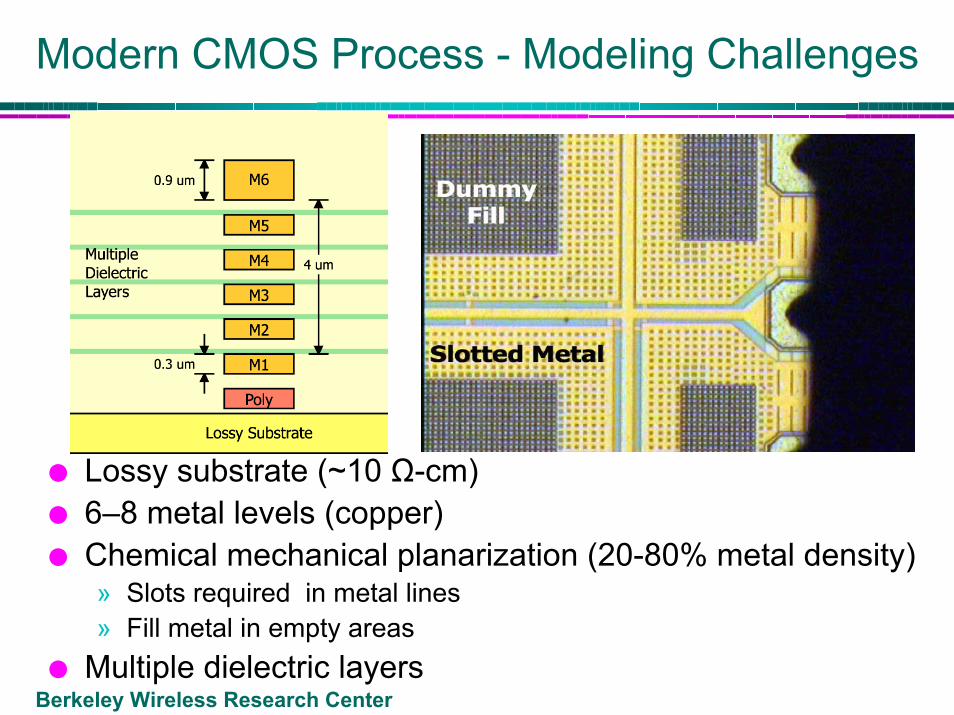
Modern CMOS Process - Modeling Challenges
Lossy substrate (~10 Ω-cm)6–8 metal levels (copper)Chemical mechanical planarization (20-80% metal density)» Slots required in metal lines » Fill metal in empty areas
Multiple dielectric layers
Berkeley Wireless Research Center
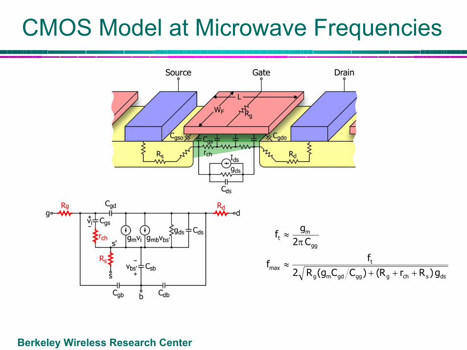
CMOS Model at Microwave Frequencies
dsschggggdmg
tmax
gg
mt
g)RrR()CCg(R2f
f
C2g
f
+++≈
π≈
Berkeley Wireless Research Center
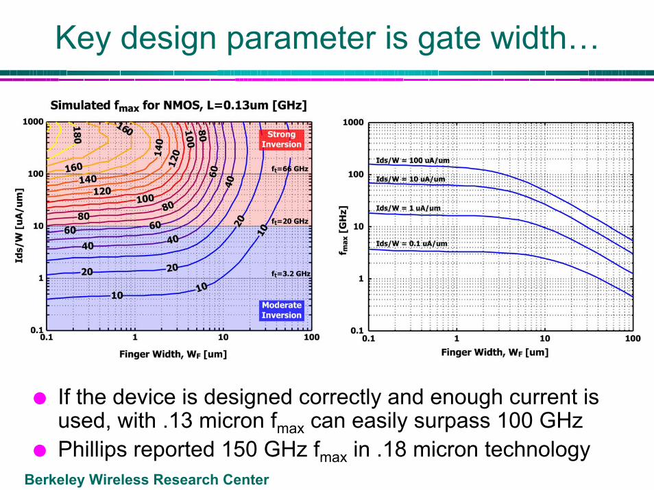
Key design parameter is gate width…
If the device is designed correctly and enough current is used, with .13 micron fmax can easily surpass 100 GHzPhillips reported 150 GHz fmax in .18 micron technology
Berkeley Wireless Research Center
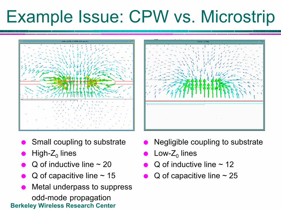
Example Issue: CPW vs. Microstrip
Small coupling to substrateHigh-Z0 linesQ of inductive line ~ 20Q of capacitive line ~ 15Metal underpass to suppress odd-mode propagation
Negligible coupling to substrateLow-Z0 linesQ of inductive line ~ 12Q of capacitive line ~ 25
Berkeley Wireless Research Center
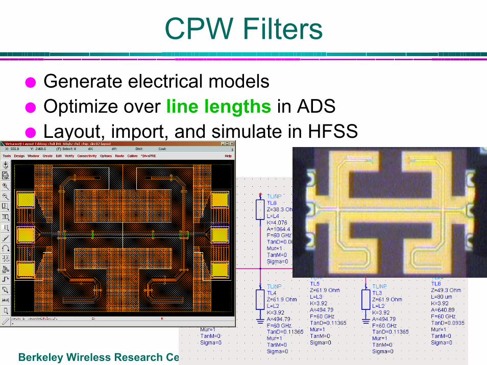
CPW FiltersGenerate electrical modelsOptimize over line lengths in ADSLayout, import, and simulate in HFSS
Berkeley Wireless Research Center
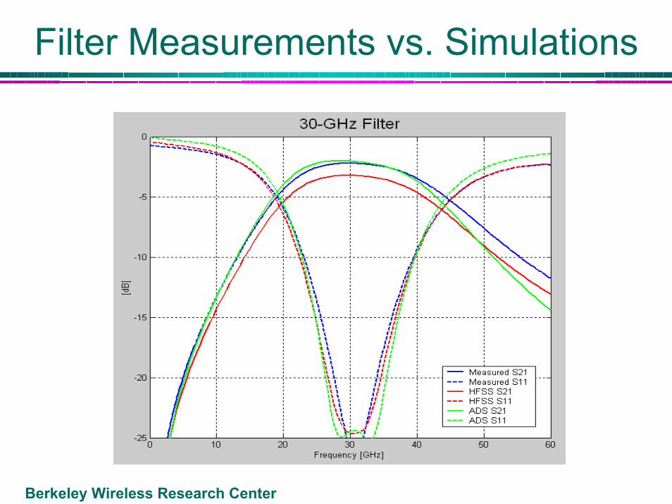
Filter Measurements vs. Simulations
Berkeley Wireless Research Center
Now that we know CMOS can do it: The open question is…
What is the best way to use 5 GHz of bandwidth to implement a high datarate link?» Extremely inefficient modulation but at a very
high rate? (say 2 GHz of bandwidth for 1 Gigabit/sec) – requires analog processing
» Or use an efficient modulation, so lower bandwidth. e.g. OFDM – but needs digital processing and a fast A/D
Berkeley Wireless Research Center
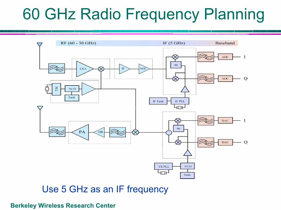
60 GHz Radio Frequency Planning
Use 5 GHz as an IF frequency
Berkeley Wireless Research Center
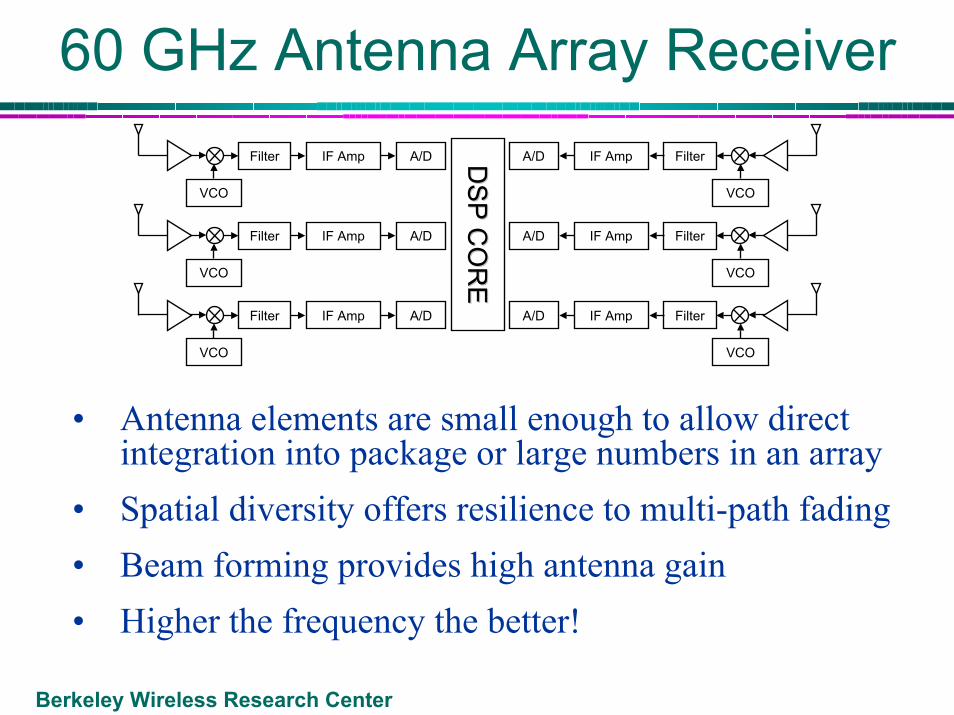
60 GHz Antenna Array Receiver
VCO
Filter IF Amp A/D
VCO
Filter IF Amp A/D
VCO
Filter IF Amp A/D
VCO
FilterIF AmpA/D
VCO
FilterIF AmpA/D
VCO
FilterIF AmpA/D
DSP C
OR
ED
SP CO
RE
• Antenna elements are small enough to allow direct integration into package or large numbers in an array
• Spatial diversity offers resilience to multi-path fading• Beam forming provides high antenna gain • Higher the frequency the better!
Berkeley Wireless Research Center
ConclusionsUWB radios provide a new way to utilize the spectrum and there is a wide variety of unique applications of this technology
However, it takes a completely new kind of radio design…
At the present state of technology CMOS is able to exploit the unlicensed 60 GHz band
However, what kinds of systems should be built with all this bandwidth
There is 19 GHz of bandwidth ready to be used for those willing to try something new!