Embed Size (px)
Citation preview
A 6.75 – 7.25 GHz Pulse Position Modulation Ultra-Wideband
Receiver Front End
David DuRussel
Osama Khan
Mark Swiderski
DuRussel, Khan, Swiderski EECS 522
OutlineIntroduction
MotivationPulse Position Modulation
• System OverviewDesign SpecificationsIndividual Stage Design
ConclusionResultsDesign ChallengesQuestions
DuRussel, Khan, Swiderski EECS 522
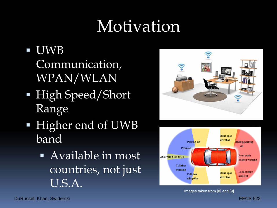
Motivation
DuRussel, Khan, Swiderski EECS 522
UWB Communication, WPAN/WLANHigh Speed/Short RangeHigher end of UWB band
Available in most countries, not just U.S.A.
Images taken from [8] and [9]
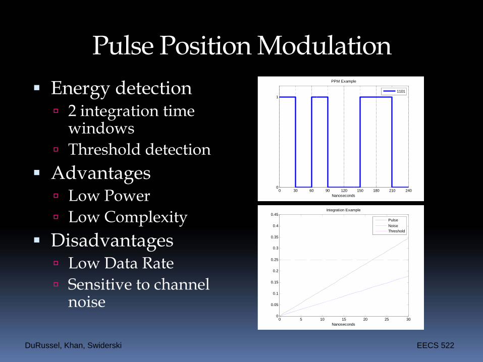
Pulse Position ModulationEnergy detection
2 integration time windowsThreshold detection
AdvantagesLow PowerLow Complexity
DisadvantagesLow Data RateSensitive to channel noise
DuRussel, Khan, Swiderski EECS 522
0 30 60 90 120 150 180 210 2400
1
Nanoseconds
PPM Example
1101
0 5 10 15 20 25 300
0.05
0.1
0.15
0.2
0.25
0.3
0.35
0.4
0.45
Nanoseconds
Integration Example
PulseNoiseThreshold
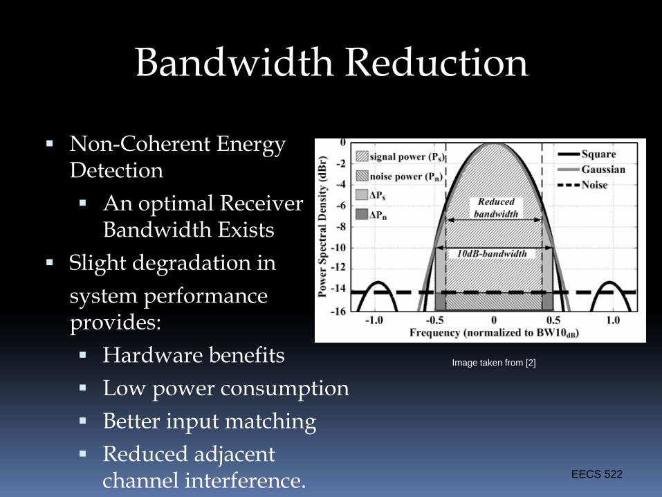
Bandwidth Reduction
Non-Coherent Energy Detection
An optimal Receiver Bandwidth Exists
Slight degradation in system performance provides:
Hardware benefitsLow power consumptionBetter input matchingReduced adjacent channel interference.
Image taken from [2]
EECS 522
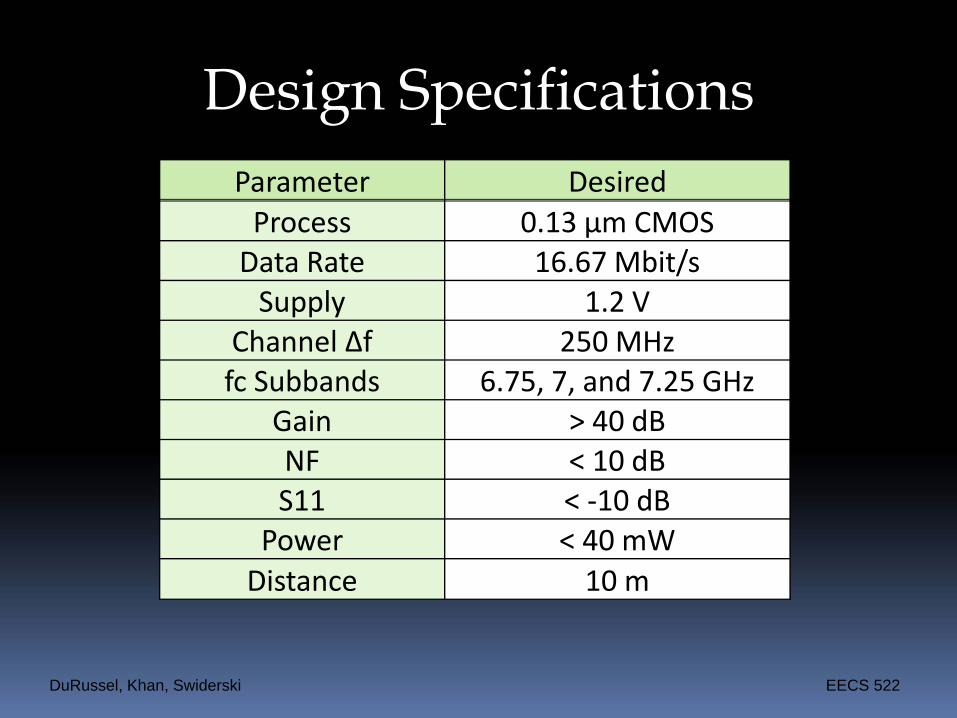
Design Specifications
DuRussel, Khan, Swiderski EECS 522
Parameter DesiredProcess 0.13 µm CMOSData Rate 16.67 Mbit/sSupply 1.2 V
Channel Δf 250 MHzfc Subbands 6.75, 7, and 7.25 GHz
Gain > 40 dBNF < 10 dBS11 < ‐10 dB
Power < 40 mWDistance 10 m
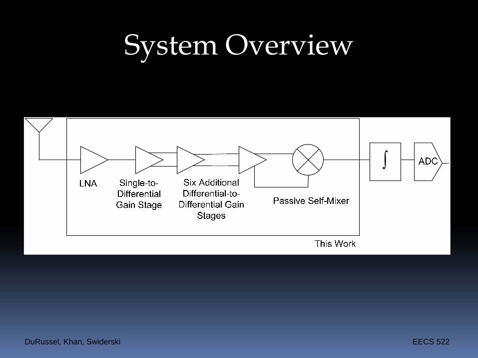
System Overview
DuRussel, Khan, Swiderski EECS 522
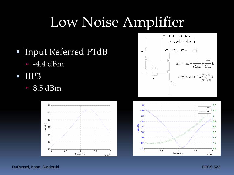
Low Noise Amplifier
DuRussel, Khan, Swiderski EECS 522
1 gmZin sL LsCgs Cgs
= + +
min 1 2.4 ( )T
F γ ωα ω
≈ +
Input Referred P1dB -4.4 dBm
IIP3 8.5 dBm
6 6.5 7 7.5 8
x 109
-24
-22
-20
-18
-16
-14
-12
-10
-8
Frequency
S11
(dB
)
6 6.5 7 7.5 8
x 109
2.4
2.5
2.6
2.7
2.8
2.9
3
3.1
3.2
S11NF
6 6.5 7 7.5 8
x 109
10
12
14
16
18
20
22
Frequency
Gai
n (d
B)

Low Noise Amplifier
DuRussel, Khan, Swiderski EECS 522
Overall NF < 2.6 dBOverall Return Loss > 15 dB
Noise Figure and S11
Controllable Gain Stages
DuRussel, Khan, Swiderski EECS 522
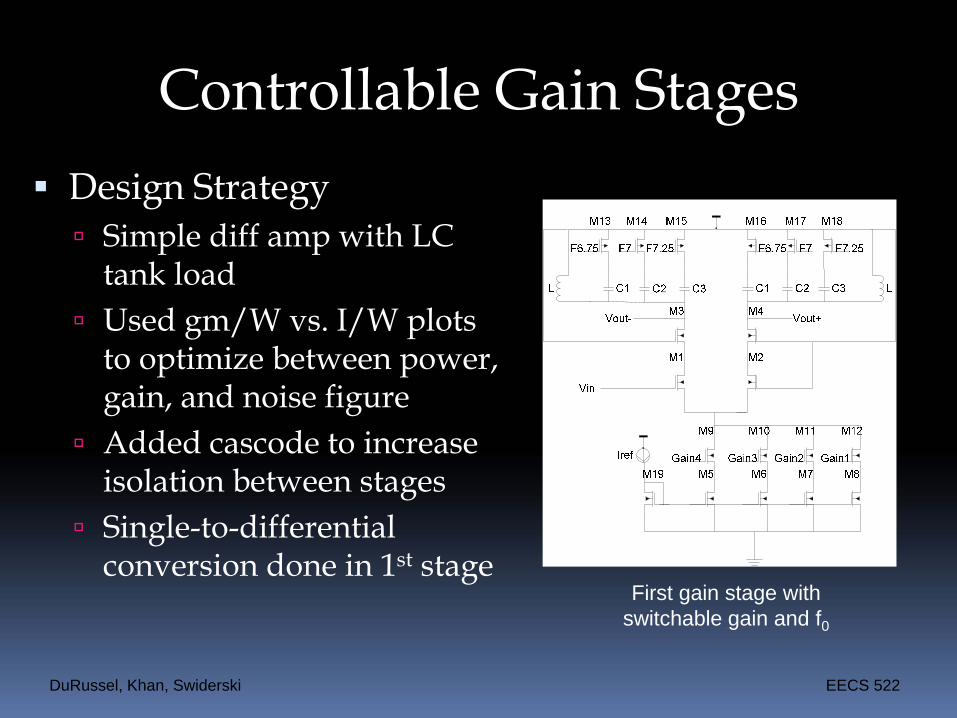
Design StrategySimple diff amp with LC tank loadUsed gm/W vs. I/W plots to optimize between power, gain, and noise figureAdded cascode to increase isolation between stagesSingle-to-differential conversion done in 1st stage
First gain stage with switchable gain and f0
Controllable Gain Stages
DuRussel, Khan, Swiderski EECS 522
Proper Functionality of Gain Control Proper Functionality of Channel Selection
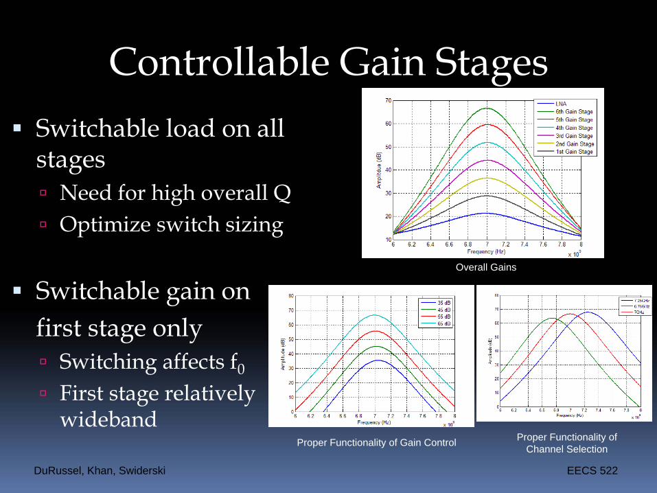
Switchable load on all stages
Need for high overall QOptimize switch sizing
Switchable gain on first stage only
Switching affects f0
First stage relatively wideband
Overall Gains
Self-Mixer
DuRussel, Khan, Swiderski EECS 522
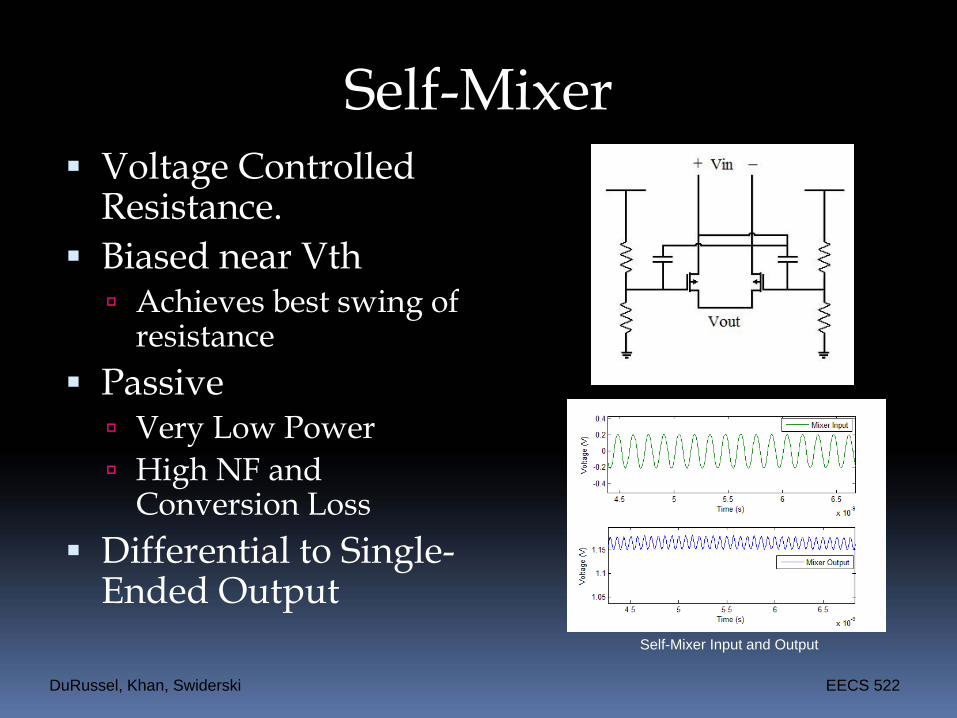
Voltage Controlled Resistance.Biased near Vth
Achieves best swing of resistance
PassiveVery Low PowerHigh NF and Conversion Loss
Differential to Single-Ended Output
Self-Mixer Input and Output
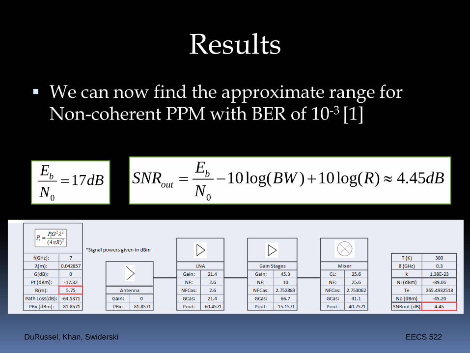
ResultsWe can now find the approximate range for Non-coherent PPM with BER of 10-3 [1]
DuRussel, Khan, Swiderski EECS 522
0
17bE dBN
=0
10 log( ) 10log( ) 4.45bout
ESNR BW R dBN
= − + ≈
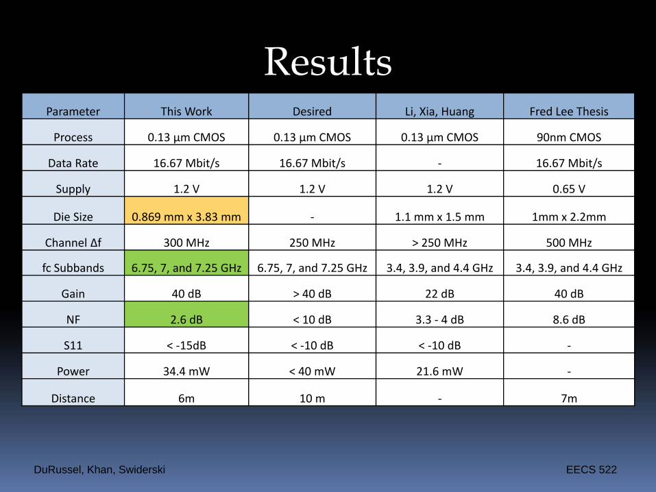
Results
DuRussel, Khan, Swiderski EECS 522
Parameter This Work Desired Li, Xia, Huang Fred Lee Thesis
Process 0.13 µm CMOS 0.13 µm CMOS 0.13 µm CMOS 90nm CMOS
Data Rate 16.67 Mbit/s 16.67 Mbit/s ‐ 16.67 Mbit/s
Supply 1.2 V 1.2 V 1.2 V 0.65 V
Die Size 0.869 mm x 3.83 mm ‐ 1.1 mm x 1.5 mm 1mm x 2.2mm
Channel Δf 300 MHz 250 MHz > 250 MHz 500 MHz
fc Subbands 6.75, 7, and 7.25 GHz 6.75, 7, and 7.25 GHz 3.4, 3.9, and 4.4 GHz 3.4, 3.9, and 4.4 GHz
Gain 40 dB > 40 dB 22 dB 40 dB
NF 2.6 dB < 10 dB 3.3 ‐ 4 dB 8.6 dB
S11 < ‐15dB < ‐10 dB < ‐10 dB ‐
Power 34.4 mW < 40 mW 21.6 mW ‐
Distance 6m 10 m ‐ 7m
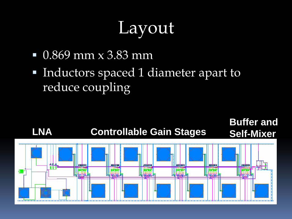
Layout
LNA Controllable Gain StagesBuffer and Self-Mixer
0.869 mm x 3.83 mmInductors spaced 1 diameter apart to reduce coupling
Design Challenges
Upper Band Channel SelectionHigh Q, Narrow Bandwidth
Center Frequency TuningChannel and Gain SwitchesMixer CharacterizationDie Size
DuRussel, Khan, Swiderski EECS 522
Conclusions
Specifications reasonably met or exceededVery low noise figureGood input matching, gain, and BW
Large die sizeFuture Work
Differential InductorsHigher order filters
Fewer Gain Stages
DuRussel, Khan, Swiderski EECS 522
Questions
DuRussel, Khan, Swiderski EECS 522
References1. F. S. Lee, “Energy Efficient Ultra-Wideband Radio Transceiver Architectures and
Receiver Circuits” PhD Thesis, Department of Electrical Engineering and Computer Science, Massachusetts Institute of Technology, Cambridge, MA, 2007.
2. J. M. Almodovar-Faria and D. D. Wentzloff, “Optimal Filter Bandwidth for Non-Coherent UWB Receivers,” Unpublished.
3. G. Palmisano and S. Pennisi, “CMOS single-input differential-output amplifier cells,” Circuits, Devices and Systems, IEE Proceedings, 6 June 2003, pp. 194-198.
4. K. Han, L. Zou, Y. Liao, H. Min and Z. Tang, “A Wideband CMOS Variable Gain Low Noise Amplifier Based on Single-to-Differential Stage for TV Tuner Applications,” Solid-State Circuits Conference, 2008. A-SSCC ’08. IEEE Asian, 3-5 Nov. 2008, pp. 457-460.
5. T. H. Lee, The Design of CMOS Radio-Frequency Integrated Circuits, 2nd ed., Cambridge University Press, 2003.
6. Raúl Blázquez, “Ultra-wideband Digital Baseband”, PhD Dissertation, Massachusetts Institute of Technology, 2006.
7. W. Li, L. Xia, Y. Huang and Z. Hong, “A 0.13um CMOS UWB Receiver Front-End Using Passive Mixer,” Circuits and Systems, 2008. APCCAS 2008. IEEE Asia Pacific Conference, pp. 288-291.
8. http://www.sara-group.org/operating_principle9. http://www.engadget.com/tag/UltraWideband/
DuRussel, Khan, Swiderski EECS 522


![INSTRUCTION MANUAL - RC DEPOT MANUAL Wingspan: 60 in [1520mm] Wing Area: 606 in2 [39dm2] Weight: 6.75 – 7.25 lb [3060 – 3290g] Wing Loading: 26 – 28 oz/ft2 [79 – 85g/dm2] Length:](https://img.pdfslide.us/doc/110x75/5c9654e409d3f221118c136e/instruction-manual-rc-manual-wingspan-60-in-1520mm-wing-area-606-in2-39dm2.jpg)


![[UTSOA] enews 7.25](https://img.pdfslide.us/doc/110x75/5695d0281a28ab9b02913b07/utsoa-enews-725.jpg)