Embed Size (px)
Citation preview

An 8 GHz Ultra Wideband Transceiver Testbed
by
Deepak Agarwal
Thesis submitted to the Faculty of the
Virginia Polytechnic Institute and State University
in partial fulfillment of the requirements for the degree of
Master of Science
in
Computer Engineering
Dr. Peter M. Athanas, Chair
Dr. Steven W. Ellingson
Dr. Cameron D. Patterson
October 7, 2005
Blacksburg, Virginia
Keywords: ultra-wideband, software radio, FPGA, high-speed datapath
Copyright 2005, Deepak Agarwal

An 8 GHz Ultra Wideband Transceiver Testbed
Deepak Agarwal
(ABSTRACT)
Software defined radios have the potential of changing the fundamental usage model
of wireless communications devices, but the capabilities of these transceivers are of-
ten limited by the speed of the underlying processors and FPGAs. This thesis presents
the digital design for an impulse-based ultra wideband communication system capa-
ble of supporting raw data rates of up to 100 MB/s. The transceiver is being developed
using software/reconfigurable radio concepts and will be implemented using commer-
cially available off-the-shelf components. The receiver uses eight 1 GHz ADCs to
perform time interleaved sampling at an aggregate rate of 8 Gsamples/s. The high
sampling rates present extraordinary demands on the down-conversion resources.
Samples are captured by the high-speed ADC and processed using a Xilinx Virtex-
II Pro (XC2VP70) FPGA. The testbed has two components: a non real-time part
for data capture and signal acquisition, and a real-time part for data demodulation
and signal processing. The overall objective is to demonstrate a testbed that will al-
low researchers to evaluate different UWB modulation, multiple access, and coding
schemes. As proof-of-concept, a scaled down prototype receiver which utilized 2 ADCs
and a Xilinx Virtex-II Pro (XC2VP30) FPGA was fabricated and tested.

Acknowledgments
I would like to express my sincere gratitude to Dr. Peter M. Athanas, who has been
one of the most patient and helpful guides one can ask for. It has been a great learning
experience for me and I am grateful to him for giving me this opportunity to work in
Configurable Computing Lab at Virginia Tech. I would also like to thank Dr. Steven
W. Ellingson and Dr. Cameron Patterson for their guidance and appreciate their will-
ingness to serve on my committee.
I would like to thank all the past and present members of CCM lab who made my stay
in the lab a memorable one. This thesis could not have been accomplished without
their support. Above all, I would like to thank to my parents and family for all their
love and guidance. They have been a never-ending source of support and encourage-
ment and I am truly blessed to be surrounded with such great people.
iii

Contents
1 Introduction 1
1.1 Overview of Ultra Wideband (UWB) Radio . . . . . . . . . . . . . . . . . 1
1.2 Contributions . . . . . . . . . . . . . . . . . . . . . . . . . . . . . . . . . . 5
1.3 Organization of Thesis . . . . . . . . . . . . . . . . . . . . . . . . . . . . . 7
2 Background 8
2.1 Software Defined Radio . . . . . . . . . . . . . . . . . . . . . . . . . . . . . 9
2.2 Ultra Wideband Systems . . . . . . . . . . . . . . . . . . . . . . . . . . . . 15
2.3 High Performance FPGA Designs . . . . . . . . . . . . . . . . . . . . . . . 20
3 Advanced Ultra Wideband Receiver 23
3.1 Introduction . . . . . . . . . . . . . . . . . . . . . . . . . . . . . . . . . . . 24
3.1.1 Digital Receiver Topologies . . . . . . . . . . . . . . . . . . . . . . 26
iv

3.2 Sampling and Clock Distribution . . . . . . . . . . . . . . . . . . . . . . . 27
3.2.1 Sampling Techniques . . . . . . . . . . . . . . . . . . . . . . . . . . 27
3.2.2 Analog to Digital Converter . . . . . . . . . . . . . . . . . . . . . . 30
3.2.3 PCB Clock Distribution . . . . . . . . . . . . . . . . . . . . . . . . 30
3.3 RF Front End . . . . . . . . . . . . . . . . . . . . . . . . . . . . . . . . . . 31
3.4 ADC to FPGA Interface . . . . . . . . . . . . . . . . . . . . . . . . . . . . . 32
3.4.1 UWB Pulse Characteristics . . . . . . . . . . . . . . . . . . . . . . 32
3.4.2 Receiver Sampling . . . . . . . . . . . . . . . . . . . . . . . . . . . 32
3.4.3 ADC FPGA Interface Timing . . . . . . . . . . . . . . . . . . . . . 33
3.5 FPGA Clock Domains . . . . . . . . . . . . . . . . . . . . . . . . . . . . . . 36
3.6 UWB Communication Protocol Frame Structure . . . . . . . . . . . . . . 37
3.7 Acquisition . . . . . . . . . . . . . . . . . . . . . . . . . . . . . . . . . . . . 39
3.7.1 Data Capture Infrastructure . . . . . . . . . . . . . . . . . . . . . 40
3.7.2 Coarse Acquisition . . . . . . . . . . . . . . . . . . . . . . . . . . . 41
3.7.3 Fine Acquisition . . . . . . . . . . . . . . . . . . . . . . . . . . . . . 45
3.8 Synchronization . . . . . . . . . . . . . . . . . . . . . . . . . . . . . . . . . 47
3.9 Real-Time Tracking . . . . . . . . . . . . . . . . . . . . . . . . . . . . . . . 48
v

3.10 Data Demodulation . . . . . . . . . . . . . . . . . . . . . . . . . . . . . . . 49
3.10.1 DDR Registers . . . . . . . . . . . . . . . . . . . . . . . . . . . . . . 50
3.10.2 Data Synchronizers . . . . . . . . . . . . . . . . . . . . . . . . . . . 50
3.10.3 Partial Correlation Unit (PCU) . . . . . . . . . . . . . . . . . . . . 52
3.10.4 Dynamic Resource Scheduler . . . . . . . . . . . . . . . . . . . . . 54
3.10.5 Coefficient Template . . . . . . . . . . . . . . . . . . . . . . . . . . 55
3.10.6 Adder Tree and Comparator . . . . . . . . . . . . . . . . . . . . . . 56
3.11 Output Interface . . . . . . . . . . . . . . . . . . . . . . . . . . . . . . . . . 57
3.12 Design Timing and Results . . . . . . . . . . . . . . . . . . . . . . . . . . 57
3.13 Results . . . . . . . . . . . . . . . . . . . . . . . . . . . . . . . . . . . . . . 58
4 Prototype UWB Receiver 62
4.1 Motivation . . . . . . . . . . . . . . . . . . . . . . . . . . . . . . . . . . . . 62
4.2 Prototype Receiver Board Overview . . . . . . . . . . . . . . . . . . . . . 64
4.3 Prototype Development Design Methodology . . . . . . . . . . . . . . . . 66
4.3.1 Development Platform . . . . . . . . . . . . . . . . . . . . . . . . . 66
4.3.2 Design Migration . . . . . . . . . . . . . . . . . . . . . . . . . . . . 68
4.4 Test and Evaluation . . . . . . . . . . . . . . . . . . . . . . . . . . . . . . . 69
vi

4.4.1 Initial FPGA Configuration . . . . . . . . . . . . . . . . . . . . . . 69
4.4.2 Verify Power Distribution System Operation . . . . . . . . . . . . 72
4.4.3 RS-232 Interface . . . . . . . . . . . . . . . . . . . . . . . . . . . . 73
4.4.4 FPGA Data Capture Infrastructure . . . . . . . . . . . . . . . . . 75
4.4.5 DC Input Data Capture . . . . . . . . . . . . . . . . . . . . . . . . 78
4.4.6 Data Capture with Sinusoidal Input . . . . . . . . . . . . . . . . . 81
4.4.7 Data Capture with a UWB Pulse Input . . . . . . . . . . . . . . . 87
4.4.8 Conclusions . . . . . . . . . . . . . . . . . . . . . . . . . . . . . . . 87
5 Conclusion and Future Work 90
5.1 Future Work . . . . . . . . . . . . . . . . . . . . . . . . . . . . . . . . . . . 92
5.2 Conclusion . . . . . . . . . . . . . . . . . . . . . . . . . . . . . . . . . . . . 93
Bibliography 94
vii

List of Figures
1.1 FCC mandated spectral mask for UWB communication systems. . . . . 3
2.1 Block diagram of a Software Defined Radio . . . . . . . . . . . . . . . . . 9
2.2 Block diagram of an ideal Software Radio . . . . . . . . . . . . . . . . . . 10
3.1 TI sampling and reconstruction of an analog signal using an array of
four ADCs [1] . . . . . . . . . . . . . . . . . . . . . . . . . . . . . . . . . . 29
3.2 Block diagram of the Software-Defined Ultra Wideband Communication
System, from [2] . . . . . . . . . . . . . . . . . . . . . . . . . . . . . . . . . 33
3.3 Timing diagram illustrating the ADC data buses and the FPGA DDR
clock signals. . . . . . . . . . . . . . . . . . . . . . . . . . . . . . . . . . . . 37
3.4 The experimental communication protocol Frame Structure chosen for
advanced SDR receiver, from [2] . . . . . . . . . . . . . . . . . . . . . . . . 38
viii

3.5 Block diagram of the Digital Processing Hardware for the UWB Com-
munication System . . . . . . . . . . . . . . . . . . . . . . . . . . . . . . . 39
3.6 Block diagram of FPGA data capture for Acquisition . . . . . . . . . . . . 41
3.7 Block diagram of the Synchronizer that transfers data from local sam-
ple clock to global clock domain . . . . . . . . . . . . . . . . . . . . . . . . 51
3.8 Block diagram of the Partial Correlation Unit (PCU) . . . . . . . . . . . 53
3.9 Timing report extracted from the Xilinx place-and-route results for the
data demodulation unit . . . . . . . . . . . . . . . . . . . . . . . . . . . . . 59
3.10 Area report extracted from the Xilinx place-and-route results for the
data demodulation unit . . . . . . . . . . . . . . . . . . . . . . . . . . . . . 60
3.11 A snapshot of Xilinx FPGA Editor: The ADC data buses drives pins on
the right quadrants of the FPGA . . . . . . . . . . . . . . . . . . . . . . . 61
4.1 Prototype Ultra Wideband Receiver . . . . . . . . . . . . . . . . . . . . . 65
4.2 Block diagram of the prototype receiver board . . . . . . . . . . . . . . . 65
4.3 LEDs blinking in a programmed pattern verified that the FPGA had
been properly configured . . . . . . . . . . . . . . . . . . . . . . . . . . . . 71
4.4 Output from Minicom which verified that the FPGA was able to com-
municate to a host PC using the RS-232 interface . . . . . . . . . . . . . 74
ix

4.5 Block diagram of FPGA data capture infrastructure tested using a pseudo-
sample generator . . . . . . . . . . . . . . . . . . . . . . . . . . . . . . . . 76
4.6 Output from Minicom which verified that all FPGA data capture infras-
tructure was fully operational. Infrastructure was tested by inputting
a pseudo-sample sequence which is seen in the data stream above. . . . 77
4.7 Output of the ADCs when a 50Ω dummy load is connected to the UWB
In input. Note the slight gain and offset mismatch . . . . . . . . . . . . . 79
4.8 Block diagram of FPGA data capture from individual ADCs . . . . . . . 82
4.9 Captured output from ADC#1 and ADC#2 for a 12 MHz CW input at a
sampling frequency of 500 MHz . . . . . . . . . . . . . . . . . . . . . . . . 83
4.10 Block diagram of FPGA data capture with ADC sample de-interleaving. 84
4.11 Time-Interleaved output of the prototype receiver PCB for a 127 MHz
CW input at an effective sampling frequency of 1 GHz. . . . . . . . . . . 86
4.12 Time-Interleaved output of the prototype receiver PCB for a 151 MHz
CW input at an effective sampling frequency of 2 GHz. . . . . . . . . . . 86
4.13 Comparison of a UWB pulse sampled by a Tektronix oscilloscope and
the same UWB pulse sampled by the prototype receiver. . . . . . . . . . 88
x

List of Tables
3.1 Partial Correlation Unit Resource Schedule . . . . . . . . . . . . . . . . . 55
xi

Chapter 1
Introduction
1.1 Overview of Ultra Wideband (UWB) Radio
Ultra wideband (UWB) is a fast emerging technology with unique features that make
it an attractive alternative for a variety of short-range high data rate applications. An
ultra wideband system can be broadly classified as any communication system whose
instantaneous bandwidth is many times greater than the minimum required to de-
liver a particular information rate. Despite the renewed interest in the last decade,
UWB systems have a long history of use in military applications and radio. The basic
research in this field was done in 1960s by Gerald Ross [3] while working for Sperry
Rand Corporation, who was granted the pioneering patent for a UWB transceiver in
1973 [4]. Hence this technology has been around for more than 30 years. However,
1

Deepak Agarwal Chapter 1. Introduction 2
the scarce bandwidth resources meant that the inefficient use of bandwidth relegated
UWB systems to experimental work for a very long time. This changed with the FCC’s
2002 First Report and Order (R&O) [5] that released huge spectral range between 3.6-
10.1 GHz at the noise floor for UWB applications. In this approved frequency range,
the UWB radios can coexist with present RF systems using low power pulses.
FCC gave a formal definition of UWB as any wireless scheme with instantaneous
spectral occupancy in excess of 500 MHz, or fractional bandwidth (BW /fc) of more than
20%, where BW is the transmission bandwidth and fc is the center frequency. Further-
more, this system must meet the spectrum mask shown in Figure 1.1. These Effective
Isotropic Radiated Power (EIRP) levels are established by considering the power spec-
trum of emitting sources in each frequency range and keeping it low enough to avoid
any interference. Further experiments are required to determine the actual interfer-
ence cause by UWB signals. UWB communication systems have three key features
which distinguish them from conventional narrowband systems [6].
• Large instantaneous bandwidth enables fine time resolution for use as a radar,
for imaging, or for precision location capability.
• Short-duration pulses prevent signal fading (fluctuations in the received signal
power) in very harsh communication environments.
• Low transmitter power and very wide bandwidths allows coexistence with exist-

Deepak Agarwal Chapter 1. Introduction 3
Figure 1.1: FCC mandated spectral mask for UWB communication systems.

Deepak Agarwal Chapter 1. Introduction 4
ing users and provides Low Probability of Intercept (LPI).
The advantages of UWB technology have been recognized by the radar and communi-
cation community for a long time [3][7][8]. It offers unique capabilities which can be
harnessed for applications in communications, radar, positioning systems and imag-
ing. The large spectral bandwidth opens the door for a large number of bandwidth-
hungry applications and high data rate communication systems. UWB signals have
low spectral density with low probability of detection (LPD), which makes it espe-
cially useful for military applications. It can resolve multipath delay values in the
nanosecond range, which allows for finer resolution in precision imaging and naviga-
tion systems. This property is also exploited for imaging of steel structures embedded
within walls, for surveillance, and for medical monitoring. The spread spectrum ca-
pability of UWB along with the ability to resolve multipath fading makes it ideal for
short range wireless communication in harsh environments.
Traditionally, UWB system implementations are impulse based and utilize a variety
of modulation schemes to transfer data. Despite the FCC intervention to regulate the
frequency range and power levels of UWB signals, there is still no industry consensus
on other aspects of these communication systems. There is a major effort underway
by the IEEE 802.15 group to standardize UWB wireless radio for indoor multimedia
applications. There are two competing standards: orthogonal frequency division mul-
tiplexing (OFDM) where the information is conveyed by spreading data transmission

Deepak Agarwal Chapter 1. Introduction 5
across multiple carriers; and impulse-UWB where impulse like signals in the time-
domain are used. Multiple access schemes such as Time Hop Multiple Access (THMA)
can be used to provide communication access to many users simultaneously.
1.2 Contributions
This thesis presents the digital design for a flexible UWB transceiver testbed using
a Xilinx Virtex-II Pro XC2VP70 FPGA. Although all blocks for this design were not
tested in hardware, this thesis gives an adequate insight into the proposed design.
The communication system was designed to sample the UWB pulse at 8 Gsps, and
the FPGA designs are capable of demodulating it in real-time. As an intermediate
step, a scaled down version of the testbed was fabricated and successfully tested with
lower data rates. The main contributions of this thesis are listed below.
• Provided an insight from the digital design perspective into a feasible Printed
Circuit Board (PCB) design which can handle high I/O bandwidth and sample
rates expected from the system.
• Implemented the digital design and debugged the proof-of-concept initial pro-
totype Software Defined Radio (SDR) receiver. This prototype consists of a Xil-
inx XC2VP30 FPGA and samples the incoming analog signal at 2 GHz using

Deepak Agarwal Chapter 1. Introduction 6
two Time-Interleaved Analog to Digital Converters (ADC). The Xilinx Embed-
ded Development Kit (EDK) and ML310 FPGA prototyping board were used as
the development platform for these designs.
• Developed an acquisition and synchronization scheme that can be controlled by
the embedded PowerPC processors in non real-time mode. Though this task
is performed in non real-time using a PowerPC processor, the oscillator drift
creates timing constraints that limit the amount of processor cycles available to
complete this task.
• Developed a feasible dataflow architecture for the Advanced SDR Receiver. To
handle data rates of 64 Gbps in real-time, the entire synchronous design should
be capable of clocking at 250 MHz. There are 16 ADC sample data buses which
are clocked using 16 different clock domains; hence, a careful design that avoids
metastability issues is essential. It also includes an early-late gate technique
for real-time tracking between transmitter and receiver.
• Implemented the datapath for the final SDR receiver and ensure that it is ca-
pable of clocking at the target frequency of 250 MHz. This should be done us-
ing minimal FPGA resources so that future developers can add error correction,
multiple access and modulation schemes. Additional constraints and techniques
that were required by Xilinx tools to achieve the target throughput were also de-
termined.

Deepak Agarwal Chapter 1. Introduction 7
1.3 Organization of Thesis
Chapter 1 contains an overview of UWB Radio, motivation for the project and contri-
butions of the thesis. Chapter 2 provides the background information on Software
Radios, and surveys state-of-the-art in UWB architectures and high-speed datap-
ath FPGA implementations. Chapter 3 contains a detailed discussion of the pro-
posed digital design for the UWB transceiver. The sampling scheme, limitations of
Commercial-Off-The-Shelf (COTS) based designs, ADC and clock networks, acquisi-
tion and synchronization, demodulator design, real-time tracking of the UWB pulse
train and external interfaces are discussed. In Chapter 4, the design of the prototype
board is discussed. The motivation for fabricating this intermediate board, design
considerations, the testing and evaluation and some results are provided. Chapter 5
gives a summary of research efforts and discusses future research directions in this
area.

Chapter 2
Background
This chapter presents an overview of the underlying concepts for the implementa-
tion of the SDR-based UWB transceiver testbed. It discusses the characterstics and
benefits of a software defined radio. The next section outlines the evolution of UWB
technology and lists some of the state-of-the-art UWB systems. A Xilinx FPGA was
used to implement the digital datapath for the UWB communication system. The last
section discusses the advantages of using an FPGA for implementing high through-
put datapaths, along with a discussion of some recent such implementations.
8

Deepak Agarwal Chapter 2. Background 9
Figure 2.1: Block diagram of a Software Defined Radio
2.1 Software Defined Radio
The advent of Software Defined Radio (Figure 2.1) has brought a paradigm shift in the
way communication radios are designed. The research in this field was kick started
by US Defense Advanced Projects Research Agency (DARPA) and targeted military
applications [9]; however, in the last decade these ideas have percolated from defense
applications into the mainstream and are considered to be important links in solving
problems in commercial wireless applications. An SDR transceiver performs most
of the baseband processing tasks like modulation/demodulation, error correction, en-
cryption/decryption and timing control in software. An ideal SDR, commonly known
as Software Radio (Figure 2.2), goes one step further and has a A/D and D/A converter
at its receive and transmit antennas; hence, the transceivers perform up-conversion
and down-conversion between baseband and RF carrier exclusively in the digital do-
main [10].
Software Defined Radio Forum [10], an international organization dedicated to pro-
moting the adoption and use of SDR, defines SDR as a collection of hardware and

Deepak Agarwal Chapter 2. Background 10
Figure 2.2: Block diagram of an ideal Software Radio
software technologies that enable reconfigurable system architectures for wireless
networks and user terminals. There still remains a lack of formal design methodol-
ogy for Software Defined Radios and most designs are based on an ad-hoc approach
that leverage the flexibility of the underlying hardware in the best possible way.
Software defined radios are considered an enabling technology that promote flexibil-
ity across the spectrum of wireless applications and offer numerous advantages over
conventional fixed radio architectures [11]. The operating parameters such as carrier
frequency, modulation schemes, error correction, and power output can be changed
without replacing the system hardware. This improved adaptability opens oppor-
tunities for reducing the cost of communication and improving services. Firmware
updates can be used to fix bugs, send upgrades, or add new features to the radio at
low cost. Such a programmable radio can also be made more secure against malicious
attacks by altering the software to make it invisible and quickly respond to such
threats. SDR allows for variation in modulation schemes and can accommodate a
number of algorithms for acquisition and synchronization, depending on the changes
in operating environment.

Deepak Agarwal Chapter 2. Background 11
SDR-based systems first gained popularity in base stations rather than handsets
which provided the perfect platform for evaluating varied radio design techniques.
The technology was considered unsuitable for mobile wireless applications like cell
phones because such applications have stringent size, weight and power requirements
that presented difficult challenges; however, over the last decade, the advances in
available hardware have helped migrate this design methodology to mobile applica-
tions. The Joint Tactical Radio System (JTRS) [12] is a US Department of Defense
initiative to design flexible radios to meet the diverse communication needs of war-
fighters. This organization has designed sophisticated communication devices that
use software programmable techniques to create high performance radios for defense
needs. Some of the capabilities [11] that have pushed software radio towards wider
acceptance are:
1. Seamless global coverage over multiple standards.
2. Support for multiple services on common hardware.
3. On-the-air upgrade capability for newer standards and protocols as well as bug
fixes.
4. Power efficient designs.

Deepak Agarwal Chapter 2. Background 12
5. Reduced cost of manufacturing and testing by using COTS components.
6. Run-Time Reconfigurability (RTR).
In context of this thesis, a SDR radio is an adaptable radio where the reconfigura-
bility is provided by a Field Programmable Gate Array (FPGA). The characteristics
of such a radio can be altered by downloading complete or partial bitstreams to the
embedded FPGA [13]. Although this is different from the classical view of a SDR that
is software programmable, it is considered a soft radio because the reconfigurability
accomplishes a similar objective, i.e. it provides a mechanism to alter the functional-
ity of the radio without replacing the hardware. A Configurable Computing Machine
(CCM) based implementation has distinct advantages compared to an Application
Specific Integrated Circuit (ASIC) or Digital Signal Processor (DSP) based implemen-
tation. The conventional software radios achieve flexibility by using software which
runs over static hardware like DSP or microprocessors; however, this approach leads
to inefficient utilization of hardware because different algorithms have distinct hard-
ware requirements. While one signal processing task might require a large number
of MAC operations, another might require fast bit twiddling or a Fast Fourier Trans-
form (FFT) core.
Lack of support for the common signal processing tasks, high power usage and low
throughput make general purpose microprocessors an unattractive choice for soft-
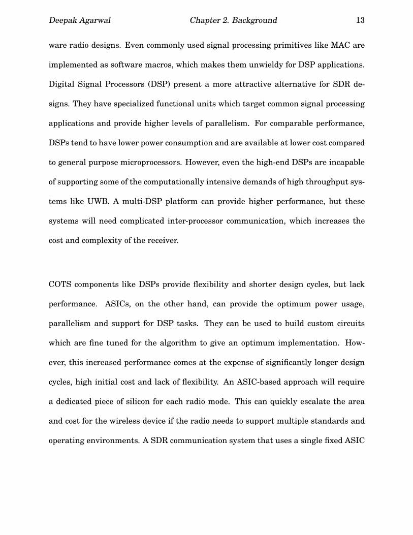
Deepak Agarwal Chapter 2. Background 13
ware radio designs. Even commonly used signal processing primitives like MAC are
implemented as software macros, which makes them unwieldy for DSP applications.
Digital Signal Processors (DSP) present a more attractive alternative for SDR de-
signs. They have specialized functional units which target common signal processing
applications and provide higher levels of parallelism. For comparable performance,
DSPs tend to have lower power consumption and are available at lower cost compared
to general purpose microprocessors. However, even the high-end DSPs are incapable
of supporting some of the computationally intensive demands of high throughput sys-
tems like UWB. A multi-DSP platform can provide higher performance, but these
systems will need complicated inter-processor communication, which increases the
cost and complexity of the receiver.
COTS components like DSPs provide flexibility and shorter design cycles, but lack
performance. ASICs, on the other hand, can provide the optimum power usage,
parallelism and support for DSP tasks. They can be used to build custom circuits
which are fine tuned for the algorithm to give an optimum implementation. How-
ever, this increased performance comes at the expense of significantly longer design
cycles, high initial cost and lack of flexibility. An ASIC-based approach will require
a dedicated piece of silicon for each radio mode. This can quickly escalate the area
and cost for the wireless device if the radio needs to support multiple standards and
operating environments. A SDR communication system that uses a single fixed ASIC

Deepak Agarwal Chapter 2. Background 14
for modulation-demodulation cannot change its characteristics without replacing the
hardware. This defeats one of the primary objectives of building a SDR as opposed
to a fixed implementation radio. Moreover, the upfront cost of designing an ASIC is
huge and the economy of scale might not kick in until large volumes are achieved.
Field Programmable Gate Arrays (FPGAs) are the mainstream configurable comput-
ing technology used to rapidly implement digital logic. These are prefabricated COTS
components that can be reprogrammed to change the hardware behavior by down-
loading a bitstream. An FPGA-based SDR implementation provides significant ad-
vantages as compared to a DSP or ASIC based implementation. It can morph the
hardware functionality to suit the needs of a particular baseband processing task for
a software radio, while still retaining maximum flexibility. Another distinguishing
feature of this technology is run-time reconfigurability. Using a modular design flow
[14], a section of the chip can be reconfigured to change the hardware functionality,
while the rest of the chip operates uninterrupted. This can eliminate any downtime
for the radio while it is being upgraded. The limitations of such architecture include
limited Input/Output (I/O) bandwidth, high per unit cost as compared to ASICs or
DSPs, higher power dissipation and lower throughput compared to ASICs.

Deepak Agarwal Chapter 2. Background 15
2.2 Ultra Wideband Systems
UWB has experienced over 40 years of technological advancement since the first work
was conducted in the field of time domain electromagnetics in the 1960s. In fact, one
can reasonably argue that the origins of the technology stem from spark discharge
transmission designs done by Marconi in the 1890s. Impulse-based radios similar to
this were the principal mechanism for sending information across air waves for more
than two decades. Though they continued to be researched and used in niche applica-
tions, eventually vacuum tubes and solid state oscillators became popular and could
be used to generate sinusoidal waves and modulate them for discriminating receivers.
In the 60s and 70s, impulse radio technology further matured and was being used for
non-communication applications and showed potential for commercial wireless appli-
cations as well.
The pioneering patent by Ross in 1973 was among the first ones that demonstrated
the utility of radio systems utilizing wide instantaneous bandwidth [4]. It transmit-
ted information by encoding an impulse train using pulse position modulation. Subse-
quent patents by Ross and other inventors further refined the subsystems required to
build this UWB radio. It was widely recognized that the baseband pulses can carry in-
formation utilizing a variety of modulation and radio schemes. Since there was prior
art involved, the patents were granted on the specific instances detailed for building

Deepak Agarwal Chapter 2. Background 16
the UWB system, rather than the baseband carrier technology itself.
With bandwidth resource being scarce, interest in UWB devices was restricted to
radar systems for military applications till the late 90s. FCC regulations restricted
the spectrum usage and the narrowband systems operate between exclusive frequency
ranges. There were a few unlicensed frequency spectrum bands, but they were not
large enough to build a wideband system. However, over the years, it was realized
that the UWB systems can co-exist without interfering with the FCC regulated nar-
rowband communication. This not only required that UWB radios have low signal
power, it also assumes that the conventional systems operate at a higher average
power and are also not subject to upsets by relatively high peak power UWB tran-
sients. In 2002 the FCC allocated a huge bandwidth spectrum between 3.1 and 10.6
GHz with regulated power levels, for UWB applications. Since then, diverse modula-
tion and access schemes have been proposed to build practical UWB communication
systems. Today, UWB systems not only exploit the available knowledge of building
impulse radios, researchers are also exploring new techniques to employ this band-
width in a useful manner. Hence, UWB is considered more of an available spectrum
for unlicensed use rather than a technology in itself. Currently, only the United States
permits the operation of UWB devices, while there are similar ongoing efforts with
the regulatory authorities in Europe and Japan.

Deepak Agarwal Chapter 2. Background 17
During ongoing negotiations for IEEE 802.15.3a standards, UWB has emerged as the
leading contender for the underlying technology. This standard will provide the spec-
ification for wireless connectivity between Personal Area Network (PAN) devices. It
is envisioned as the wireless equivalent of the Universal Serial Bus (USB) standard
and will complement the 802.11 standard, not replace it. It can be used to provide
wireless connectivity in applications such as home networking and multimedia, wear-
able computing and wireless desktops. The long term vision for UWB is a low power
high speed standard that provides wireless connectivity for battery operated devices.
Due to this underlying potential, ultra wideband technology has attracted wide spread
interest from the research community in recent years and achieved notable progress.
The advances in fabrication techniques, improved digitizers, and denser and larger
digital circuits have contributed towards improving the performance of these devices.
Despite this, any practical UWB system has to deal with implementation feasibility
issues like limited ADC bandwidth and sampling speeds, inadequate baseband pro-
cessor throughput and increased effects of digital noise. Moreover, to meet the size,
power consumption and cost demands for the mass consumer markets, a higher level
of integration is desired. A UWB system like Bluetooth, which utilizes a single chip
solution with few external, components will help drive this technology into consumer
applications.

Deepak Agarwal Chapter 2. Background 18
Presently analog/RF components of a UWB system are mostly implemented in high-
performance SiGe technology, while the digital circuits are custom designed using
standard Complementary Metal-Oxide Semiconductor (CMOS). As compared to other
fabrication technologies like SiGe, CMOS is particularly compelling due to its low-
cost, low power consumption and wide availability. Any system which utilizes it au-
tomatically benefits from the rapid shrinking of CMOS devices which follows Moore’s
law. To reduce time-to-market, it is desirable that the analog components be built
using common-place CMOS COTS components like ADCs, DACs, oscillators and am-
plifiers. Using COTS only components significantly reduces engineering time and re-
sources needed to build these components. It benefits from economy of scale and can
also utilize the standard production quality procedures already in place. As the level
of integration increases, this becomes even more pertinent since the overall device
will primarily host digital circuits built using CMOS technology. A more thorough
discussion of physical layer issues is beyond the scope of this thesis and reader is re-
ferred to [2].
A number of companies have already announced UWB products, both in the mili-
tary and consumer application domain. In the commercial domain, Xtreme Spec-
trum released the first commercial UWB solution called Trinity [15] in 2002. It
promised data rates of 100Mbps while consuming less than 200 milliwatts of en-
ergy. In 2004, Freescale released the first FCC approved commercially available

Deepak Agarwal Chapter 2. Background 19
UWB chip set XS110 [16] [17]. It is based on Direct Sequence UWB (DS-UWB) and
is targeted towards wireless home entertainment systems and mobile multimedia de-
vices. Freescale is part of a consortium of 40 companies who are building DS-UWB
based systems, which is one of the two competing standards in the commercial UWB
space. The other standard is Multiband Orthogonal Frequency Division Multiplexing
(OFDM) which is led by companies like Intel, Texas Instruments, Nokia and Philips
Semiconductors. The first silicon for Multiband OFDM Alliance (MBOA) standard
was demonstrated by Alereon Corporation in October 2004 with commercial produc-
tion expected by late 2005. Other companies who have announced prototypes are
Mobile Ad hoc Network by Multispectral Solutions Inc. and PulsON by Time Domain
Corporation. Pal650 [18], is the first commercial precision asset location system de-
veloped by Multispectral Solutions Inc. which complies with FCC regulations.
In the military domain, the Low Probability of Detection (LPD) applications have be-
come increasingly sophisticated with higher bandwidth requirements. DRACO is a
prototype high-speed multi-user UWB network which has a range of 1-2 km, depend-
ing on the environment [19]. It provides a high level of transmission security by using
a unique UWB waveform design. The latest version of DRACO uses an FPGA to im-
plement all the digital transceiver functions as well as the networking algorithms.
Another UWB network radio transceiver, ORION [20] [19], was designed with short
range and long range capabilities. It utilizes the 1-2 GHz spectrum with 30% frac-

Deepak Agarwal Chapter 2. Background 20
tional bandwidth. It is modular in design and uses an FPGA to implement the digital
part of transceiver functionality. AWICS UWB transceiver [21][19] was designed to
meet the operational wireless communication requirements of Department of Navy
onboard Navy and Marine helicopters. The requirements were especially stringent
due to multipath emanating from reflections within aircraft fuselage and rotor sys-
tem. UWB was chosen over the other available technologies due to its robustness
to multipath interference and LPD, which would prevent unauthorized intercepts.
The instantaneous bandwidth of this system was 400MHz with an effective EIRP of
+26 dbM. This system was successfully tested in February 2003 onboard multiple air-
crafts.
2.3 High Performance FPGA Designs
FPGAs have evolved at a very rapid pace over the last decade, with vendors releasing
larger and more sophisticated devices. Until the late 80s and early 90s, they were pri-
marily considered as test platforms that were used for ASIC characterization to work
out timing and functional bugs before sending the design for fabrication. FPGAs had
some niche low volume applications but those were far and between. However, with
rapid shrinking of CMOS feature size, FPGAs have not only packed more logic gates,
but integrated PowerPC cores, hard multipliers and sophisticated high speed I/O ca-

Deepak Agarwal Chapter 2. Background 21
pable of supporting multiple I/O standards. With this rapid integration, they have
reached the critical size that makes them feasible for designing complete applica-
tions. The fine grained architecture of an FPGA allows the designer to customize the
digital logic for the algorithm and extract large amount of parallelism. Dynamically
configurable FPGAs can even adapt to various computational tasks through hard-
ware reuse.
Efficient biological sequencing is one such bioinformatics task where researchers have
reported huge increase in performance by utilizing FPGAs. In one such implementa-
tion [22], the time complexity of the problem was reduced from O(mn) to O(m + n),
where m and n are the lengths of the two sequences being compared, yielding an or-
der of magnitude improvement in performance while maintaining the same level of
sensitivity. FPGAs are also ideal for high-bandwidth, high-performance streaming
applications where the processing elements must keep pace with the sensor output.
Such applications are abundantly found in the signal processing rich domains of video
streaming and signal acquisition. These real-time systems require the subsystem like
adaptive filters [23], fast Fourier transforms [24] and digital beamformers [25][26] to
keep up with the high input data rates. Video encoding according to the H.263 stan-
dard for video conferencing is one such application, where compression speeds of 120
Mbps can be achieved [27]. This is more than twice the speed of software compression
and opens doors for multi-video streaming applications using a single reconfigurable

Deepak Agarwal Chapter 2. Background 22
device.
High-performance decryptor/encryptor cores for Advanced Encryption Standard (AES)
have been demonstrated which can achieve high throughput of 4.2 Gbps using a mod-
est Xilinx Virtex-E device [28]. For elliptic curve cryptography, the point multiplica-
tion can be computed almost 500 times faster than a dual Xeon Processor [29]. These
are not isolated examples but a sustained trend over a large class of applications
varying from image processing [29] to floating point operations [30].
While speed is one of the strengths of FPGAs, there are other compelling advantages
of using them as well. These include lower power consumption as compared to a gen-
eral purpose microprocessor, faster time to market and improved upgradeability and
Run-Time Reconfigurability (RTR). These factors are decisive advantages for embed-
ded applications, and the developers of such systems have shown a growing interest
in using the reconfigurable devices. Hence, it can be safely stated that FPGAs, with
their unique ability to provide an ideal mix of functional and storage elements to
match an application, will continue to attract growing interest.

Chapter 3
Advanced Ultra Wideband Receiver
This chapter presents an outline for the design of a flexible UWB transceiver testbed,
with a specific focus on the digital datapath of the communication system. The ad-
vanced UWB communication system has been built using Software Defined Radio
concepts which provide tremendous flexibility and rapid prototyping capabilities over
a fixed hardware implementation. The heart of a SDR UWB transceiver is the digi-
tal processing hardware, as it must be capable of handling high-speed data streams
from the Analog to Digital Converters (ADCs) and then process the data in real-
time. To implement the digital part of the baseband processor, a top-of-the-line high-
performance Xilinx FPGA Virtex-II Pro XC2VP70 was chosen.
23

Deepak Agarwal Chapter 3. Advanced Ultra Wideband Receiver 24
3.1 Introduction
The overall objective of this project was to design a impulse based UWB transceiver
that could meet the following design objectives.
• Flexible implementation, so that it can be used as a testbed for experimenta-
tion with different modulation/multiple access schemes, frame structures and
receiver topologies.
• Achieve an effective raw data rate of 100 Mbps at a range of 10 meters.
• Seamless signal acquisition and synchronization between two UWB devices.
• Real-Time tracking capability to compensate for oscillator drifts between the
wireless devices.
• Capable of supporting multiple receiver topologies like Digital Leading Edge
Detection and Digital Pilot-Based Matched Filter.
• Built using only COTS components.
Currently, state-of-the-art UWB communication systems are composed of custom-
developed hardware and do not use SDR architectures. The challenges involved in
developing such as communication testbed — extremely high sampling rates, huge
amounts of input/output data, and a tremendous amount of digital processing power
— have been fairly daunting. These challenges become particularly poignant when
Deepak Agarwal Chapter 3. Advanced Ultra Wideband Receiver 25
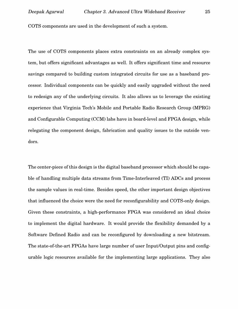
COTS components are used in the development of such a system.
The use of COTS components places extra constraints on an already complex sys-
tem, but offers significant advantages as well. It offers significant time and resource
savings compared to building custom integrated circuits for use as a baseband pro-
cessor. Individual components can be quickly and easily upgraded without the need
to redesign any of the underlying circuits. It also allows us to leverage the existing
experience that Virginia Tech’s Mobile and Portable Radio Research Group (MPRG)
and Configurable Computing (CCM) labs have in board-level and FPGA design, while
relegating the component design, fabrication and quality issues to the outside ven-
dors.
The center-piece of this design is the digital baseband processor which should be capa-
ble of handling multiple data streams from Time-Interleaved (TI) ADCs and process
the sample values in real-time. Besides speed, the other important design objectives
that influenced the choice were the need for reconfigurability and COTS-only design.
Given these constraints, a high-performance FPGA was considered an ideal choice
to implement the digital hardware. It would provide the flexibility demanded by a
Software Defined Radio and can be reconfigured by downloading a new bitstream.
The state-of-the-art FPGAs have large number of user Input/Output pins and config-
urable logic resources available for the implementing large applications. They also

Deepak Agarwal Chapter 3. Advanced Ultra Wideband Receiver 26
contain embedded hard processors, multipliers and memory which can be customized
for any DSP style operation. After careful consideration, a Xilinx XC2VP70 FPGA
was chosen for implementing the digital processor.
3.1.1 Digital Receiver Topologies
The SDR based radio design gives the user flexibility for using different receiver con-
figurations. These choices can be influenced by various factors like BER specifica-
tions, environment issues like high noise or even functional requirements. Two of
these topologies are briefly discussed below while a more detailed explanation can be
found in [1] [2].
Digital Leading Edge Detection
In this simplest of UWB receiver topologies, the incoming pulse strength is compared
with a pre-determined value. Depending on whether it crosses the threshold or not,
it is demodulated as a ‘1’ or ‘0’. This can be implemented as comparison logic using
FPGA design primitives; however, such a receiver implementation is susceptible to
noise spikes and is less secure against interference and jamming.

Deepak Agarwal Chapter 3. Advanced Ultra Wideband Receiver 27
Digital Pilot-Based Matched Filter (DPBMF)
In this technique, the expected sample values corresponding to a bit are determined
by averaging the pilot pulses. This template not only includes the original UWB
pulse, but also contains pulse distortion, multipath signals and distortions generated
by the antenna or propagation environment. For data demodulation, a matched filter
operation is performed using this template on the received date pulses.
3.2 Sampling and Clock Distribution
3.2.1 Sampling Techniques
The receiver design is based on a sampling architecture with data demodulation. The
input analog signal is sampled at a rate higher than twice the Nyquist frequency
and demodulation is performed in the digital domain. A Direct or Time-Interleaved
approach can be used to accomplish the sampling, and a detailed discussion of the
advantages/disadvantages is provided in [1][2].

Deepak Agarwal Chapter 3. Advanced Ultra Wideband Receiver 28
Direct Sampling
In this approach, a single ADC is used to sample the analog waveform at the target
sample rate. This is ideally suited for low bandwidth signals or a custom IC design
approach where the system requirements are not stringent. However, since a UWB
wireless signal has a bandwidth of several gigahertz, the sampling rates can be of the
order of ten gigahertz making this implementation infeasible for the testbed.
Time Interleaved (TI) Sampling
In TI sampling approach, multiple ADCs are used to sample a waveform at different
points in time in a round robin fashion. These ADCs operate in parallel and their
clocks are slightly offset from each other. Hence, the effective sampling rate is the
sampling rate of an ADC multiplied by the total number of ADCs. The signal is re-
constructed by the digital hardware as if it is being sampled by a single high speed
ADC. TI-Sampling is advantageous in a COTS implementation as it significantly re-
laxes the requirements on the interface between the ADCs and the FPGA while still
preserving the quality of the received signal, as illustrated in Figure 3.1 [1][2]. While
this approach increases hardware area and power consumption, the data bus and
clocks run at a much lower rate. For comparison, if an analog signal is sampled at 4
GHz with a 4-bit ADC using a Direct Sampling approach; it will require a 4 GHz 4-bit

Deepak Agarwal Chapter 3. Advanced Ultra Wideband Receiver 29
wide bus that connects the ADC output to the FPGA pins and a 4 GHz clock. How-
ever, if four of these ADCs are used, each sampling the signal at 1 GHz, then four
independent buses will carry the data to the FPGA, each running at 1 GHz. Hence
the complexity of the system has increased but the design timing is relaxed by an
order of magnitude. For these reasons, TI sampling was chosen over Direct-Sampling
for implementation on the UWB Receiver.
(a) The first ADC samples the received
signal at Point A, the second at Point B,
the third at Point C, and the fourth at
Point D.
(b) The FPGA is then able to reconstruct
the received signal as if it were sampled
by a single ADC
Figure 3.1: TI sampling and reconstruction of an analog signal using an array of four
ADCs [1]

Deepak Agarwal Chapter 3. Advanced Ultra Wideband Receiver 30
3.2.2 Analog to Digital Converter
After careful consideration, MAXIM MAX104 ADC [31] was chosen for the Advanced
SDR Receiver. This ADC offers an input bandwidth of 2.2 GHz with a maximum sam-
pling rate of 1 GHz. The samples have 8-bit quantization and can be demultiplexed
over two output data buses, each running at half the sampling frequency. The aper-
ture delay for these ADCs is 100 ps with less than 30% part-to-part variation and the
gain and offset is adjustable so that a bank of ADCs can be matched accurately. More-
over these high-performance ADCs were available for a reasonable cost as compared
to similar offerings from other major vendors.
3.2.3 PCB Clock Distribution
The performance of TI sampling technique is highly dependent on sampling the re-
ceived signal at precisely spaced intervals. An ultra-low skew clock distribution net-
work with tight tolerances on jitter values is required to accurately reconstruct the
received signal. Additionally, since the successive ADCs require a clock out-of-phase
by 125 ps, precise delay needs to be inserted in each clock signal. In most cases, the
FPGA Digital Clock Manager (DCM) can be used to drive such high precision clock
networks, hence eliminating the need for any extra delay components. However, the
current state-of-the-art FPGAs have DCMs with jitter specs in the order of 100ps and

Deepak Agarwal Chapter 3. Advanced Ultra Wideband Receiver 31
they cannot meet the stringent tolerance requirements for this design.
The clock network [2] for this board was achieved using On Semiconductor’s MC100LVEP14
1:5 low-skew clock driver. This clock distribution chip has a typical Output-to-Output
skew of 25 ps while the clock jitter value is less than 2 ps RMS. The clock delay for
successive ADCs is adjusted using On Semiconductor’s MC10E195 programmable de-
lay chip. This chip provides a maximum delay of 10 ns with a digitally selectable
delay step resolution of 10 ps, with a less than 5 ps RMS jitter value. Additionally,
constraint driven routing of the clock signals on the PCB ensures that all clock traces
are synchronized and the skew values are low.
3.3 RF Front End
The RF front end [2] is comprised of several broadband amplifiers, variable atten-
uators and filters and feeds the received signal to the ADCs; however, a thorough
discussion of this subsystem is beyond the scope of this thesis.

Deepak Agarwal Chapter 3. Advanced Ultra Wideband Receiver 32
3.4 ADC to FPGA Interface
3.4.1 UWB Pulse Characteristics
Since the maximum input bandwidth for the Maxim ADCs is 2.2 GHz (minimum
pulse width of 480 ps), the UWB pulse width for this communication system was cho-
sen to be 500 ps corresponding to bandwidth of 2 GHz. A UWB pulse is transmitted
every 10 ns to achieve the target data rate of 100 Mbps.
3.4.2 Receiver Sampling
To accurately reconstruct the 500 ps wide UWB pulse in the digital domain, the sig-
nal should be sampled at well over twice the Nyquist frequency. A sampling rate of 8
GHz was chosen and was implemented with eight Maxim ADCs using a TI sampling
approach described above. Each ADC operates in parallel at 1 GHz, where the suc-
cessive ADCs sample the signal at an offset of 125 ps, giving an effective sampling
rate of 8 GHz. This is illustrated in the Figure 3.2. The demultiplexer feature allows
one to clock the data buses at half the sampling frequency, i.e. 500 MHz, which eases
the input timing requirements for the FPGA. The use of more buses makes the digital
hardware more complex, but as subsequent analysis will show, this is essential, since
even at 500 MHz databus rates, the envelope for FPGA design is being pushed.

Deepak Agarwal Chapter 3. Advanced Ultra Wideband Receiver 33
Figure 3.2: Block diagram of the Software-Defined Ultra Wideband Communication
System, from [2]
3.4.3 ADC FPGA Interface Timing
The MAX104 ADCs have an integrated demultiplexer that produces samples on a
primary and auxiliary bus, each operating at half the sampling frequency (i.e. 500
MHz). The ADC also asserts a data ready (DREADY) signal, which is in-phase with
the data. The DREADY signals are offset by 125 ps and are used as a clock in the
FPGA to capture the ADC sample data. To input data at such high speeds, the FPGA
uses Double Data Rate (DDR) registers operating at half the DREADY frequency (i.e.

Deepak Agarwal Chapter 3. Advanced Ultra Wideband Receiver 34
250 MHz). Due to analog RF constraints, all of the ADCs buses are connected to
I/O Buffers (IOBs) on only two quadrants of the FPGA. Even though the use of DDR
registers relaxes the clock requirement to 250 MHz, the data remains stable for 2 ns
and must be latched within this time frame; however, the following factors reduce the
available time to reliably capture the data.
1. Due to the asymmetric placement of the ADCs with respect to the FPGA, the
differential data bus signals have unequal lengths. Hyperlynx simulations [2]
demonstrated that the worst case difference in wire lengths translates into a
skew of approximately 200 ps.
2. Inside the FPGA, the sampling clocks are routed over the global clock network
resources, where the skew has been minimized by design. Nevertheless, the
balancing is not perfect and some skew exists, the worst case estimate for which
is 200 ps.
3. The ADC data bus drives the FPGA pins using the LVDS I/O logic standard.
Simulations showed the worst case signal rise time for these data buses as 200
ps [2].
4. The setup time for the IOB registers for a Xilinx XC2VP70 FPGA with speed
grade −6 is 860 ps [32]. Hence, the data needs to be stable 860 ps before the
clock edge for it to be latched appropriately.
5. The DCMs used to deskew and phase align the incoming clock have a worst

Deepak Agarwal Chapter 3. Advanced Ultra Wideband Receiver 35
case clock jitter of 200 ps on clock outputs and this can adversely effect the
functioning of the DDR registers.
6. The phase shift feature of the DCMs is used to align the sample clock edge to the
ADC data bus for latching the data appropriately. At a frequency of 250 MHz,
the minimum time resolution for phase shift is approximately 15 ps.
7. The clock to data delay for the ADCs has a part-to-part variation of 400 ps;
however, since each data bus will use its own respective sample clock, this delay
remains constant for a particular ADC and will not effect the timing.
8. The hold time for the FPGA IOB registers is −630 ps [32]. A negative hold time
implies that the data is not expected to stay stable after the clock edge, and
since its magnitude is less than the setup requirement, it does not affect design
timing.
Factoring in all the skew and jitter (which is additive), the available time window for
latching in the data is reduced to 325 ps.
Tavailable = Tvalid − Tskew − Tjitter − Tsetup − Tphaseresolution
Tavailable = 2ns − 200ps(1) − 200ps(2) − 200ps(3) − 860ps(4) − 200ps(5) − 15ps(6)
Tavailable = 325ps
To meet these stringent timing requirements, the constant phase shift feature of the
DCM will be used to optimally place the clock edge so that the data integrity is main-

Deepak Agarwal Chapter 3. Advanced Ultra Wideband Receiver 36
tained. Since such precise control over the clock phase is required, each ADC clock
uses a different DCM, and the exact phase shift will be determined experimentally.
3.5 FPGA Clock Domains
The Xilinx XC2VP70 FPGA has eight DCMs and sixteen global clocking networks.
Out of these, eight independent clocks can be routed to any of the four quadrants of
the Xilinx part on the global low skew network. For other clocks or high load lines,
synthesis directives can be used to route them over the secondary low skew network.
The FPGA receives eight pairs of data buses (primary and auxiliary bus from an
ADC) clocked at 500 MHz. Each clock will have a dedicated DCM that will deskew
the clock and phase shift it to align it with the incoming data. The CLKIN DIV BY 2
attribute will be used to divide the incoming clock to 250 MHz. Each DCM produces
2 clock outputs (Clk0 and Clk180), yielding a total of 16 local clocks in the FPGA. The
phase relationship between incoming data, DCM clocks and DDR Register values is
illustrated in Figure 3.3. In the figure, PReg0 refers to the DDR register that latches
data from the Primary ADC Bus (PBus) using DCM output Clk0. Similarly, PReg180
is the DDR Register that latches data from PBus using DCM output Clk180. Similar
signals have also been shown for the Auxiliary Data Bus (ABus). Besides these local
clocks, the FPGA design uses three global clocks which are routed over the global low

Deepak Agarwal Chapter 3. Advanced Ultra Wideband Receiver 37
Figure 3.3: Timing diagram illustrating the ADC data buses and the FPGA DDR
clock signals.
skew network:
1. 300MHz clock for the PowerPC core and related logic.
2. 100MHz clock for the Processor Local Bus (PLB) and PLB peripherals.
3. 250 MHz clock for performing data demodulation.
3.6 UWB Communication Protocol Frame Structure
For development purposes, a communication protocol frame structure for the UWB
testbed was chosen so that the performance and stability of the system could be eval-
uated. This specific frame structure does not influence any design decisions that may
preclude the user from developing custom interfaces suitable for their task. Figure
3.4 illustrates the experimental UWB frame structure. It consists of a frame which
has 48 pilot pulses, 960 data pulses and guard time slots at the end of pilot pulses
as well as at the end of the frame. The length of these guard slots is equal to time
duration of eight pulses, but no pulses are transmitted in this duration. Two such

Deepak Agarwal Chapter 3. Advanced Ultra Wideband Receiver 38
Figure 3.4: The experimental communication protocol Frame Structure chosen for
advanced SDR receiver, from [2]
frames are combined together to form a superframe, allowing the system to provide
multiple users access to the radio using TDMA.
The DPBMF receiver topology, which was chosen for implementation on the Advanced
UWB receiver, has four important aspects: acquisition, synchronization, data demod-
ulation and real-time tracking. Figure 3.5 is a block diagram for the digital processing
hardware for the advanced UWB radio.

Deepak Agarwal Chapter 3. Advanced Ultra Wideband Receiver 39
Figure 3.5: Block diagram of the Digital Processing Hardware for the UWB Commu-
nication System
3.7 Acquisition
Data demodulation in a DPBMF based scheme requires that the receiver locks onto
the phase of the transmitted signal. It should precisely know when the transmitter
starts sending a new bit so that the template can be aligned to the incoming sample
values for data demodulation. This functionality is provided by the acquisition stage.
To establish the communication link, User 1 broadcasts an acquisition signal, which
consists of N UWB pulses that are amplitude modulated by a maximal-length se-
quence (m-sequence) [33]. User 1 will continue broadcasting the acquisition sequence
until it receives an acknowledgement signal from the receiver User 2. To acquire
the transmitted signal, the FPGA in User 2’s receiver will capture a set of samples

Deepak Agarwal Chapter 3. Advanced Ultra Wideband Receiver 40
equal to N UWB pulses and stores them in Block RAM (BRAM) internal to the FPGA.
Capturing N samples guarantees that at least one complete m-sequence will be cap-
tured, though the starting point of the m-sequence will be unknown. Control is then
passed to the embedded PowerPC processor. The acquisition stage is performed in
non real-time mode, i.e. once the pre-determined number of samples is collected, the
receiver does not capture any new incoming sample values but processes the captured
sequence.
3.7.1 Data Capture Infrastructure
On receiving a trigger signal, the FPGA starts registering the ADC buses and cap-
tures a pre-determined number of samples for communication system signal acquisi-
tion and stores it in FPGA internal BRAMs. Figure 3.6 shows the block diagram for
ADC data capture infrastructure. Each DDR register is associated with an exclusive
16 kB dual port memory; each implemented using eight FPGA BRAMs. The memory
has two access ports; Port A is running off the global clock and stores the incoming
DDR data, while the Port B is connected to the Processor Local Bus (PLB) and ac-
cessed by PowerPC to read the sample values. Since Port A has a 64-bit data width,
the capture controller collects eight sample values from each ADC and writes it the
memory every 8th cycle. Once the BRAM is full, it goes into the suspend state and
waits for the next trigger.

Deepak Agarwal Chapter 3. Advanced Ultra Wideband Receiver 41
Figure 3.6: Block diagram of FPGA data capture for Acquisition
3.7.2 Coarse Acquisition
Once the sample values are stored in the FPGA memory, the PowerPC processor per-
forms a sliding correlation operation using the stored template waveform. The tem-
plate sample values are initialized as a constant array and stored in the PowerPC
data cache for quick access. While the PowerPC is performing sliding correlation, the
sample values stored in BRAMs do not change. SampleCount, which is a PowerPC

Deepak Agarwal Chapter 3. Advanced Ultra Wideband Receiver 42
readable Device Control Register (DCR), helps keep track of the number of samples
that have been skipped while the PowerPC is performing coarse acquisition. The
strongest correlation between the template waveform and the received signal occurs
when they are perfectly aligned, and provides the starting index for the m-sequence.
The SampleCount is a free-running sample counter which initializes to an all-zero
value when the receiver starts filling the FPGA Memory with sample values and
wraps around at NP , where N is the number of UWB pulses in m-sequence and P is
the number of samples in a single UWB pulse. Since the m-sequence is sent repeat-
edly, if the PowerPC finds the starting index for the m-sequence at index K, the next
m-sequence will occur when the SampleCount holds the identical value K.
Even though acquisition is performed in non real-time, the number of processing cy-
cles that can be used is significantly restricted. The master oscillators for User 1 and
User 2 are not precisely synchronized and they may drift apart during acquisition.
This drift creates a window of uncertainty about the calculated start time of the next
m-sequence. The width of this uncertainty window is given by:
Umax = 2foscSosctelapsed
Where
Umax is the uncertainty window [Number of Samples]

Deepak Agarwal Chapter 3. Advanced Ultra Wideband Receiver 43
fosc is the frequency of the transceiver master oscillators [Hz]
Sosc is the stability of the transceiver master oscillators [Parts Per Million(PPM)]
telapsed is the time required to complete acquisition [seconds]
Experimentally, it was determined that the maximum uncertainty window that could
be tolerated was half the number of samples in a UWB pulse (i.e. 40 samples). The
master oscillator on the receiver has a frequency of 1 GHz and a stability of 20 parts
per million (ppm). Thus, the maximum allowable acquisition time is 1 ms. The Pow-
erPC processor operates at a frequency of 300 MHz. An acquisition time of 1 ms
gives the receiver 300,000 processor cycles to complete the first stage of acquisition.
For all possible starting points in the captured sample data, the PowerPC processor
computes the result of the following equation:
CK =∑
80N−1
i=0xi+Kyi
Where
K is the starting index in the captured sample data
CK is the magnitude of the correlation
xi is a captured sample value at position i
yi is a template sample value at position i
N is the number of pulses in acquisition sequence

Deepak Agarwal Chapter 3. Advanced Ultra Wideband Receiver 44
Because the duration of the received pulse is only 2 ns (16 samples), and the time
between pulses is 10 ns (80 samples), 64 samples in the template pulse have a value
of zero and contribute nothing to the correlation amplitude. To save processor clock
cycles, these extraneous samples are ignored, and the correlation is performed only
on the 16 samples that make up the ideal received UWB pulse. The m-sequence has
N UWB pulses, hence the PowerPC processor calculates CK using a nested loop with
16N iterations, where each iteration is estimated to require 25 cycles. With a UWB
pulse, successive samples are strongly correlated; thus, the starting index K can be
incremented by 8. Incrementing K by a number greater than one results in an error
of ±4 samples between the calculated and the true starting index of m-sequence. The
number of possible starting indices K is equal to:
KMAX = N(80
8) = 10N
Therefore, the total number of PowerPC cycles (Pcycles) required to complete the ac-
quisition is equal to
Pcycles = (25cycles/loop)(16N)(10N) = 4000N2
M-sequences are only of length N = 2r − 1, where r is any positive integer; hence N
can be (3, 7, 15, 31 ). A N = 7 m-sequence requires 196,000 processor cycles, whereas
a N = 15 m-sequence requires 900,000 processor cycles. Thus, N = 7 was chosen.
This processor delay yields an uncertainty window Umax of approximately 28 samples.

Deepak Agarwal Chapter 3. Advanced Ultra Wideband Receiver 45
3.7.3 Fine Acquisition
Knowing the index of maximum correlation, the number of samples missed, and the
window of uncertainty, the PowerPC processor can calculate the expected starting
point of the next m-sequence transmission. The FPGA will then capture another set of
N UWB Pulses, starting at the point in time it expects the m-sequence transmission
to begin, minus the duration of the uncertainty window. For precise triggering of
BRAMs, a mechanism using a second DCR register TriggerCount is provided. This
register has a default value of all ‘1’s which indicates an unarmed trigger. After
the coarse acquisition step, PowerPC writes the expected starting index value to the
TriggerCount. Writing the value to the sample register sets the trigger count as well
as arms it. When the SampleCount value is equal to the TriggerCount, the following
events take place:
• A single-cycle pulse is generated which then triggers the capture controller,
which starts filling the FPGA memory with new set of ADC sample data.
• The TriggerCount register gets set to all ‘1’s, hence disarming it.
• The SampleCount register gets reset to all ‘0’s, to keep it in step with the cap-
tured samples.
For example, if the m-length sequence has NP samples, where N is the number of
UWB pulses in m-sequence and P is the number of samples in a single UWB pulse,

Deepak Agarwal Chapter 3. Advanced Ultra Wideband Receiver 46
the coarse acquisition will find the starting index at i where 0 ≤ i < NP . If the win-
dow of uncertainty is calculated as 28 cycles, the starting index icapture for capturing
the next set of samples for fine acquisition is given by icapture = (i−28) mod NP . icapture
is written to the TriggerCount DCR register, which arms the trigger mechanism and
captures a new set of samples.
To find the starting index of the m-sequence, the processor will again perform a slid-
ing correlation similar to coarse acquisition step, with the exception that K is incre-
mented by 4. This creates an uncertainty window of ±2 sample offset, which will
be compensated by the tracking loop outlined in the subsequent synchronization and
data modulation steps. The maximum number of correlations performed for the fine
acquisition step is 0.25Umax. With Umax = 28, seven correlations will be performed,
which will require a total of about 20,000 processor cycles.
Once fine acquisition has successfully completed, User 2 will send an acknowledge
signal to User 1. The User 1 receives the acknowledge signal and transmits a series
of test frames that contain a special pilot sequence. These test frames are demodu-
lated by User 2, and the output verified to ensure it was received error free. If so,
User 2 will send a second acknowledge signal to User 1 and data transmission will
commence. If the coarse or fine acquisition step fails, the PowerPC will trigger the
capture controller, obtain a fresh set of samples and perform the entire acquisition

Deepak Agarwal Chapter 3. Advanced Ultra Wideband Receiver 47
sequence again.
3.8 Synchronization
The PowerPC Processor takes 20,000 cycles to perform fine acquisition, which creates
an uncertainty window of three samples due to oscillator drift between the receiver
and transmitter. This is fine tuned by the synchronization routine using the tracking
loop and data demodulation hardware described in subsequent sections.
Once User 1 receives the acknowledge signal indicating that User 2 has successfully
performed fine acquisition, it sends a series of test frames, the starting time for which
is the next scheduled transmission of the m-sequence. These test frames contain a
set of pilot pulses whose structure is known to the receiver beforehand. User 2, after
sending the acknowledge signal to User 1 indicating the end of acquisition step, waits
for a reasonable amount of time and demodulates the incoming test frames. This
demodulation step achieves two objectives.
• The tracking module fine tunes the synchronization between receiver and trans-
mitter by using the data demodulation hardware.
• After successful demodulation of pilot pulses, the samples are averaged to form
a template which compensates for any pulse distortions and multipaths.

Deepak Agarwal Chapter 3. Advanced Ultra Wideband Receiver 48
3.9 Real-Time Tracking
Once the synchronization is established, the receiver and transmitter are locked and
the communication system is ready for data transfer. However, due to oscillator drifts,
the receiver and transmitter can lose synchronization over time. The receiver com-
pensates for this gradual loss of synchronization using an early-late gate algorithm
[1]. Matched template correlation is performed using three template waveforms gen-
erated as follows:
1. One template advanced in time by one sample
2. One template with ideal timing
3. One template delayed in time by one sample
The template with the strongest correlation has the best alignment with the trans-
mitter. If the Case 1 template shows the strongest correlation, the receiver has fallen
behind by one sample while if Case 3 shows the strongest correlation, the receiver is
ahead by one sample. If the strongest correlation occurs with delayed or early tem-
plate consistently, the receiver needs to adjust timing to compensate for it. An early
and late count register is updated every time the non-ideal templates correlate better
than the ideal one, and if this count crosses a threshold value, the dynamic scheduler
and the coefficient template shift register chains are shifted to compensate for the
loss of synchronization.

Deepak Agarwal Chapter 3. Advanced Ultra Wideband Receiver 49
3.10 Data Demodulation
Data demodulation is performed by a Digital Pilot-Based Matched Filter (DPBMF)
receiver, which is similar to the Matched Filtering receiver that has been used in
narrowband communications for many years [34]. Matched filtering is performed by
multiplying and integrating the received pulse with the template waveform, and then
comparing the result to the receiver decision statistic threshold [34].
Mathematically, the operation is given by:
Z =∑
79
i=0xiyi
Where
x represents the ith ADC sample value
y represents the ith template sample value
In the case of binary signal transmission, Z > 0 means that a ‘1’ was transmitted and
Z < 0 means that a ‘0’ was transmitted. The data demodulation consists of a number
of elements which have been described below.

Deepak Agarwal Chapter 3. Advanced Ultra Wideband Receiver 50
3.10.1 DDR Registers
Inside the FPGA, the incoming ADC samples are evenly spread over 32 DDR Input
registers corresponding to the 16 incoming ADC data buses (PBus and ABus for each
of the eight ADCs). Because the number of samples per pulse is 80, which is not a
multiple of the number of DDR registers (32), the registers alternate between captur-
ing three samples and two samples. For example, consider ADC0 PBus. If the DDR
register running on Clk0 captures sample numbers 3, 35, 67 on the even numbered
UWB pulses and sample numbers 19, 51 on odd numbered pulses, the DDR register
running on Clk180 will capture sample numbers 19, 51 on even numbered pulses
and sample numbers 3, 35, 67 on odd numbered pulses. All other ADCs follow an
identical sequence. The DDR registers which provide samples in between 0 and 15
for the even numbered pulse are called in-phase DDR pipelines, while the ones which
provide 16-31 samples are labeled out-of-phase. Hence in the example above, ADC0
PBus DDR0 is in-phase while ADC0 PBus DDR180 is out-of-phase.
3.10.2 Data Synchronizers
The ADC data bus is aligned to the incoming ADC sample clock, and is latched into
the DDR registers using the positive and negative edge of this clock. Since finding the
complete correlation over the entire UWB pulse requires combining the partial sums

Deepak Agarwal Chapter 3. Advanced Ultra Wideband Receiver 51
Figure 3.7: Block diagram of the Synchronizer that transfers data from local sample
clock to global clock domain
from each DDR data pipeline, the DDR data has to be moved from the local sample
clock domains to a global clock domain. To avoid metastability issues, the DDR reg-
isters are fed into a simple synchronizer which can move data safely from the local
sample clock domain to a global clock domain. The global clock is the ADC0 clock
whose leading edge comes earlier in time than all the other ADC clocks.
In the first step, the synchronizer demultiplexes the incoming sample onto two buses,
each running at 125 MHz and out of phase by 180. A divide-by-2 counter is used

Deepak Agarwal Chapter 3. Advanced Ultra Wideband Receiver 52
to generate the clock enable signals as illustrated in Figure 3.7. Once the data has
been down-sampled to 125 MHz, a multiplexer alternately selects the data bus which
changed on the last local clock edge, and hence is the more stable of the two buses.
The output of the multiplexer is then latched safely into the global clock domain.
When the clocks are perfectly offset from each other by 125 ps, in the worst case, this
scheme will provide 3 ns to move data between local and global clock domains, while
avoiding any metastability issues.
3.10.3 Partial Correlation Unit (PCU)
Each DDR register has three identical dedicated data processing pipelines, which can
compute the partial correlation sum from the samples from that particular register
for the on-time, early, and late templates. The main components of this pipeline are
illustrated in Figure 3.8. It is comprised of one 8 × 8 multiplier, two 8-bit registers
to store the incoming sample values and template sample values, one 16-bit adder,
a 16-bit Multiplexer and a partial sum 16-bit output register. The control input is
driven by the dynamic resource scheduler and has two purposes.
1. It is used as the Select input for the multiplexer whose output drives one of the
accumulator inputs. For the in-phase DDR register, a sequence of 0,1,1,0,1 is
generated on the control input, which generates the partial sum every 3rd and

Deepak Agarwal Chapter 3. Advanced Ultra Wideband Receiver 53
Figure 3.8: Block diagram of the Partial Correlation Unit (PCU)
5th cycle. For an out-of-phase pipeline a sequence of 0,1,0,1,1 is generated on
the control input which generates a partial sum every 2nd and 5th cycle.
2. A ‘0’ on the control input indicates that a valid partial sum is available at the
accumulator output and the pipeline output register is updated with this new
value.
The Template Shift Register Chain, which provides the correct coefficient values to
the PCU for calculating the partial correlation, is described below.

Deepak Agarwal Chapter 3. Advanced Ultra Wideband Receiver 54
3.10.4 Dynamic Resource Scheduler
The Dynamic Resource Scheduler provides control input for the Partial Correlation
Unit (PCU). Conceptually, the resource scheduler is a simple state machine which has
five states and transitions from state zero to four in round robin fashion. Depending
on the alignment of the samples for the UWB pulse with the DDR registers, the sched-
uler sends the appropriate control signals to each of the 32 DDR PCUs to accumulate
two or three correlation values before latching it into the PCU output register. The
schedules for both in-phase and out-of-phase pipelines are illustrated in Table 3.1.
Since real-time tracking shifts the start index for the pulse sample values, the sched-
ule can dynamically change with time. For example consider the case where ADC0
PBus DDR0 (PBus0 0) is in-phase and provides the 0, 32, 64 sample for the even
numbered pulse and 16, 48 for the odd numbered pulse. In this case, the ADC0
Pbus DDR180 (PBus0 180) is out-of-phase and will provide the 16, 64 samples for
the even numbered pulse, and 0, 32, 64 for the odd numbered pulse. If the real-time
tracking module detects a better correlation with delayed coefficient template, the re-
ceiver has drifted by one sample and ADC1 PBus DDR0 (PBus1 0) will now provide
the first sample. Hence PBus0 0 pipeline will now follow the out-of-phase schedule,
while the Pbus0 180 pipeline is in-phase and the corresponding schedules have to be
adjusted.

Deepak Agarwal Chapter 3. Advanced Ultra Wideband Receiver 55
The scheduler can be implemented as a 1-bit circular shift register of length 180 (5
bits for each of the 32 DDR registers). The bits 0, 32, 64, 96, 128 correspond to the
Pbus0 0, 1, 33, 65, 97, 129 correspond to Pbus1 0 and so on. At reset the sched-
uler shift register chain is initialized assuming Pbus0 0 is the start index for the
even-numbered pulse. After synchronization, if the first sample for the UWB pulse is
predicted to arrive at position j, where 0 ≤ j < 80, the shift register chain is shifted
right j times to align the schedule with incoming sample values.
Table 3.1: Partial Correlation Unit Resource Schedule [35]State Register (R) Multiplier (M) Adder (A) Final Result (FR)
0x0 (R,y−32) (0,M) FR[Pulse−2]
x16 (R,y−16) (A,M)
1x32 (R,y0) (A,M)
x48 (R,y16) (A,M)
2x64 (R,y32) (0,M) FR[Pulse−1]
x80 (R,y48) (0,M) FR[Pulse−1]
3x96 (R,y64) (A,M)
x112 (R,y80) (A,M)
4x128 (R,y96) (A,M)
x144 (R,y112) (0,M) FR[Pulse0]
Entries in Bold are specific to the in-phase PCU
Entries in Italics are specific to the out-of-phase PCU
3.10.5 Coefficient Template
The coefficient template values are stored in an 8-bit circular shift register chain of
length 80. It has a 8-bit data input InitVal, and three control signals, ShiftRight,
ShiftLeft and LoadEn. To initialize the shift register chain, the LoadEn control input

Deepak Agarwal Chapter 3. Advanced Ultra Wideband Receiver 56
is asserted for 80 cycles and the consecutive template values are driven to the InitVal
data port. The ShiftLeft and ShiftRight control inputs are asserted by the early-late
tracking module to align the template waveform to the incoming samples.
3.10.6 Adder Tree and Comparator
In the second stage of processing, a pipelined adder tree of depth five is used to com-
bine the results from all the DDR PCUs and produce a single correlation value. This
result is compared to the decision statistic threshold and the result is stored in a
BRAM. Since the first stage of adder tree is driven by the PCU output registers which
only change every two or three clock cycles, the synchronous paths from the PCU out-
put to stage one adder output is declared as a multi-cycle path with period equal to
twice the global clock frequency. A clock enable is used to update the adder output
registers whenever a new partial correlation value is available. This does not have
any functional significance, but improves timing for the entire design. The same prin-
ciple is used throughout the five stages of adder tree to declare multi-cycle paths and
improve design timing.

Deepak Agarwal Chapter 3. Advanced Ultra Wideband Receiver 57
3.11 Output Interface
Two output interfaces are provided for debugging and data transfer functionality. Af-
ter data demodulation, the data bits are stored in a PLB BRAM. The second PowerPC
processor can then read these values and send them over a USB 2.0 interface to the
host computer. A RS-232 interface is also provided as a backup debugging interface.
3.12 Design Timing and Results
The digital baseband processor presented the daunting challenge of designing a com-
plex datapath capable of clocking at 250 MHz. Though the individual building blocks
like adders, multipliers, multiplexers are all capable of clocking at this high frequency
on an FPGA, the timing degrades quickly once they are combined together. Placement
and routing of a design on an FPGA is a NP -complete problem; hence, it is not possi-
ble to explore the entire solution space to find the best possible solution. Instead, the
back-end tools use a set of heuristics to achieve a solution that is close to optimum.
However, this approach might not work for high-speed FPGA designs where the tim-
ing constraints are very stringent. The following measures were taken to make sure
that timing closure was achieved.
1. The fanout for the nets in the design was restricted to five during the front end
synthesis stage. For high fanout nets like clock enable, the synthesis tool was

Deepak Agarwal Chapter 3. Advanced Ultra Wideband Receiver 58
forced to replicate logic which dramatically improved timing on these paths.
2. After the first place-and-route run, the timing critical paths were identified and
additional pipeline registers were added.
3. Though the entire design is clocked at 250 MHz, some of the synchronous paths
like adder trees change value every other cycle. All these paths were identified
and appropriate clock enable signals were generated and added. These were
declared as multi-cycle paths in the Xilinx constraints file.
4. Area constraints were added for the PCU Units associated with each ADC, so
that they are placed in a cluster near the corresponding IOBs.
5. The design was slightly over-constrained, i.e. a clock cycle of 3.9 ns was specified
instead of 4.0 ns (250 MHz).
6. Guided place-and-routing was used once the results from the back-end tools in-
dicated that the design had very few timing errors.
3.13 Results
Using the techniques outlined in the previous section, the design consisting of the
data demodulation unit was able to achieve the target frequency of 250 MHz. Figure
3.9 is the timing section of Xilinx place-and-route report. It illustrates that the slow-
est single-cycle critical path in the design is capable of clocking at 254 MHz (3.928 ns).

Deepak Agarwal Chapter 3. Advanced Ultra Wideband Receiver 59
Figure 3.9: Timing report extracted from the Xilinx place-and-route results for the
data demodulation unit
Another important design objective was to keep the FPGA utilization low, so that fu-
ture developers can utilize the unused FPGA resources to implement different UWB
schemes. Figure 3.10, a screenshot of the area section of the Xilinx PAR report, shows
that the FPGA slice utilization for the entire data demodulation unit is 25%. This
leaves ample unused FPGA logic resources that can be utlized for future UWB sys-
tem development. Figure 3.11 is a snapshot of data demodulation logic loaded on

Deepak Agarwal Chapter 3. Advanced Ultra Wideband Receiver 60
Figure 3.10: Area report extracted from the Xilinx place-and-route results for the
data demodulation unit
Xilinx FPGA editor. Note that the design is restricted to one half of the FPGA due to
area constraints used during place-and-route. This property is especially useful since
logic can be densely packed in the left half of the FPGA without affecting the timing
of the data demodulation units.

Deepak Agarwal Chapter 3. Advanced Ultra Wideband Receiver 61
Figure 3.11: A snapshot of Xilinx FPGA Editor: The ADC data buses drives pins on
the right quadrants of the FPGA

Chapter 4
Prototype UWB Receiver
4.1 Motivation
The COTS-based implementation of the advanced UWB radio outlined in the previous
chapter is a challenging design, both from PCB and digital design perspective. The
ADCs drive sixteen 8-bit data buses and eight clock signals at 500 MHz across the
board to the FPGA I/O pins. Due to the large number of high speed transmission lines
routed on the PCB, ensuring adequate Signal Integrity (SI) is of utmost importance.
Moreover, the TI sampling approach outlined requires very fine control over clock
delays as well as skew and jitter, which is challenging to implement on a PCB using
discrete components. The ADC to FPGA interface has to be designed appropriately
such that the FPGA can latch the LVDS signals at 500 MHz, and the digital datapaths
62

Deepak Agarwal Chapter 4. Prototype UWB Receiver 63
inside the FPGA should be capable of processing the 8 Gsps data rate and demodulate
the received UWB transmission in real-time.
The design and fabrication of the advanced receiver board has a high engineering
design time and component cost. An architecture or design issue identified late in the
design cycle can result in huge cost and time overruns. Hence, it was decided that as
an intermediate step, a scaled down prototype of the advanced radio receiver would
be developed. The prototype board would help mitigate risk by providing developers
a reference platform where the various components of the advanced receiver can be
tested in an environment that closely mimics the final design. It can potentially result
in huge time and cost savings, increase the confidence level and allow us to make
tweaks to the advanced radio design. This prototype will serve multiple purposes:
• Test the feasibility of the underlying TI sampling approach at multi gigahertz
clock frequencies.
• Verify that the power distribution systems and the clock distribution networks
meet the design objectives and identify the potential problems.
• Identify the potential Signal Integrity problems by comparing the actual trace
behavior with the simulation results obtained from the Hyperlynx simulator.
• Verify the FPGA timing and DCM behavior, including any metastability issues
that may arise due to data moving across clock domains.

Deepak Agarwal Chapter 4. Prototype UWB Receiver 64
• Serve as a development platform for the Advanced UWB receiver where radio
design related experiments can be performed.
4.2 Prototype Receiver Board Overview
As a first phase of development of the advanced UWB radio testbed, a prototype re-
ceiver has been developed (Figure 4.1). This prototype receiver is a scaled down ver-
sion (Figure 4.2) of the proposed final design. It utilizes an array of two MAXIM
MAX104 ADCs, with each ADC sampling at 1 Gsps in a Time-Interleaved fashion,
to achieve an effective sampling rate of 2 Gsps. The clock distribution network and
the power supplies on the prototype are built using the same components that will
be used in the advanced receiver board. This provides an opportunity to evaluate the
performance of these components on the PCB at high clock frequencies. For data cap-
ture and demodulation, a Xilinx Virtex-II Pro XC2VP30 FPGA with speed grade −6
has been chosen. This is smaller than the XC2VP70 FPGA that will be used for the
final board design, but provides adequate logic and I/O resources for the prototype
board. UART and USB interfaces have been provided for the debugging and data
transfer functionality.

Deepak Agarwal Chapter 4. Prototype UWB Receiver 65
Figure 4.1: Prototype Ultra Wideband Receiver
Figure 4.2: Block diagram of the prototype receiver board

Deepak Agarwal Chapter 4. Prototype UWB Receiver 66
4.3 Prototype Development Design Methodology
4.3.1 Development Platform
A ML310 FPGA board and Xilinx Platform Studio (XPS) were used as the develop-
ment platform for developing the digital designs for the prototype UWB receiver.
Hardware Platform
The ML310 board is a Xilinx Virtex-II Pro XC2VP30 FPGA based system develop-
ment board in an ATX form factor. It has onboard Ethernet MAC/PHY, DDR memory,
RS-232 interface and multiple PCI slots which can be utilized for complete embed-
ded system development. Since the prototype receiver also uses a similar XC2VP30
FPGA and UART for communication, the ML310 board provides the ideal platform
to develop and test the prototype digital designs even before the receiver boards are
fabricated. The prototype receiver board has four 8-bit differential 500 MHz ADC
buses driving the FPGA input pins, which provide the sample stream for data demod-
ulation. On a ML310 board, only a small number of high-speed I/O pins are made
available to the user. Driving all the data buses from an external source, which mim-
ics the ADC data buses, is not possible. A pseudo sample generator built inside the
FPGA itself was used to provide the sample vectors for functional testing of the de-

Deepak Agarwal Chapter 4. Prototype UWB Receiver 67
signs.
Software Platform
The Xilinx Embedded Development Kit (EDK) provides the hardware/software co-
design framework and Intellectual Property (IP) for designing Xilinx FPGA designs
with embedded IBM PowerPC hard cores [36]. The Base System Builder (BSB) fea-
ture, which has native support for the ML310 board, can be used to create a base
system consisting of the processor core along with the Processor Local Bus (PLB),
On-chip Peripheral Bus (OPB) and the Device Control Register (DCR) buses. IP cores,
PLB memory and the RS-232 core, can be easily added to the design. The system is
customizable, and features such as program and data cache for the PowerPC proces-
sor, the UART Interrupt behavior and DCM characteristics can be modified using the
XPS Graphical User Interface (GUI). Besides generating the hardware design files,
the XPS also creates software libraries, a C-routine to test the system memory and
peripherals and a Makefile for compiling the hardware as well as software.

Deepak Agarwal Chapter 4. Prototype UWB Receiver 68
4.3.2 Design Migration
Once the digital designs were generated and verified on the ML310 board using inter-
nally generated test data, the designs were migrated to the prototype receiver board.
This step requires the following changes to the design:
1. The pseudo sample generator was removed and the data ports were connected
to the FPGA I/O pins that are driven by the ADC data buses.
2. The FPGA interface to the PCB components like the UART, LEDs and Reset
switch on the ML310 board is different from the prototype receiver board; hence,
the FPGA pin location constraints, drive strengths and I/O standards were mod-
ified according to the receiver board schematics.
3. The ML310 board has an onboard oscillator which provides the FPGA with a
clock signal whose frequency is 100 MHz. On the other hand, the prototype radio
FPGA receives an input clock with a frequency of 500 MHz which is divided
down to 250 MHz using the DCM attribute CLKIN DIV BY 2. Hence, DCMs
with additional attributes were added for the sample clocks, and the lock signals
were driven to LEDs on the prototype board for debugging purposes.
4. The timing constraints were modified to reflect the prototype board clocks and
the phase relationship between the two incoming ADC sample clocks.

Deepak Agarwal Chapter 4. Prototype UWB Receiver 69
4.4 Test and Evaluation
An outline of the evaluation methodology for the prototype board along with the test
results is presented below.1
4.4.1 Initial FPGA Configuration
To verify that the JTAG (IEEE 1149.1) [38] interface was connected properly to the
FPGA, a simple FPGA bitstream was generated, and downloaded via iMPACT. This
initial testing phase was set up to verify that the FPGA could be programmed suc-
cessfully, and that the FPGA operated as intended.
JTAG Interface
Early in the design process, it was decided that the FPGA configuration would be per-
formed using the JTAG interface, which is connected to J10 on the receiver PCB [38].
IMPACT and a Parallel IV cable were used to scan the JTAG chain (which consisted
of only the FPGA), and it successfully recognized the on-board Xilinx FPGA. At this
point, the bitstream was downloaded to the FPGA. LED D10, which is connected to
the FPGA’s DONE signal, turned off when the configuration was complete, and served
as a simple mechanism during the remainder of the testing process to verify that the
1A portion of this section appears in [37]

Deepak Agarwal Chapter 4. Prototype UWB Receiver 70
FPGA configurations were properly downloaded.
FPGA Operation
The downloaded bitstream used a single-ended LVCMOS clock signal from the ex-
tra global clock pins located on J14 as an input to one of the FPGA’s Digital Clock
Managers (DCMs). The clock was driven by an external off-board oscillator first at a
frequency of 25 MHz, and then at 100 MHz. The downloaded bitstream divided down
the clock signal and flashed eight of the LEDs in a specific pattern. A reset signal
from the trigger pushbutton switch (S2) was used to reset the DCM as well as the
flashing light pattern. Observation of the blinking LEDs (Figure 4.3) verified that
the following components were operating properly.
• JTAG based FPGA configuration was successful and the FPGA operated as de-
signed.
• The correct power supply voltages were connected to the correct FPGA pins.
• The FPGA Digital Clock Manager (DCM) was able to lock onto the input Global
Clock signal.
• Pressing the trigger pushbutton was able to trigger the user global reset for the
FPGA.

Deepak Agarwal Chapter 4. Prototype UWB Receiver 71
Figure 4.3: LEDs blinking in a programmed pattern verified that the FPGA had been
properly configured
• No solder joint failures on the FPGA pins connected to power, ground, or signals
used by the bitstream.
As a secondary test of the DCMs, the blinking lights bitstream was regenerated to run
off the ADC DREADY output signal (which is used as a differential clock input to the
FPGA). The ADC input clock was slowly ramped up to a maximum of 1 GHz (which
was the target operating frequency for the ADCs on the prototype receiver). Testing
the DCMs at the maximum frequency was a critically important stage, as a higher
potential for signal integrity problems exists at higher clock frequencies. In addition
to the blinking lights, the DCM’s lock signals were driven to external LEDs. The
DCMs were able to lock onto the ADC’s DREADY signal, meaning that the DREADY

Deepak Agarwal Chapter 4. Prototype UWB Receiver 72
signal met all of the minimum timing and signal integrity requirements of the DCMs.
Passing this test was extremely important, as the DREADY signals are used as the
primary clock source in the FPGA.
4.4.2 Verify Power Distribution System Operation
The primary function of the Power Distribution System (PDS) is to meet all the static
and transient current demands of all the IC’s on the PCB. Large transient current
demands are generated when multiple outputs in a given IC switch logic states simul-
taneously (known as Simultaneous Switching Outputs, or SSOs). The large transient
current demands caused by SSO—if not compensated for by the PDS—can cause tem-
porary drops in voltage levels, leading to logic errors. On the prototype receiver, three
PDSs contained a significant number of potential SSOs: the 1.5V FPGA core PDS,
the 2.5V FPGA I/O PDS, and the 3.3V ADC output PDS.
Each of these PDSs had a special connector so that a spectrum analyzer could observe
the frequency response of the PDS. Large spikes in the spectrum indicate an unmet
current demand at that particular frequency. The PDS’s were tested with a 1 GHz
square wave input to the ADCs (which maximized the number of SSOs on the ADC
outputs), and the ADC clock inputs to the FPGA running at 500 MHz, along with
an external global clock signal of 100 MHz. The analysis of the frequency spectrum
for the 1.5V PDS, 2.5V PDS and 3.3V PDS showed that the amplitude of the spikes

Deepak Agarwal Chapter 4. Prototype UWB Receiver 73
ranges from about −80 dBm to a maximum of −50 dBm. This represents a transient
voltage drop of less than 1 mV which is well within tolerable limits.
4.4.3 RS-232 Interface
The RS-232 interface is used primarily as a debugging and verification interface, as
well as an alternative to the USB interface. To test the RS-232 interface, a null-
modem cable was used to connect the RS-232 interface on the prototype board (J13)
to a serial port on the host PC. A simple FPGA design was implemented that used
the embedded PowerPC processor to perform a simple memory test and transmit the
results to the host PC via a UART soft core. The UART core used is a proprietary Xil-
inx core which incorporates features described in National Semiconductor PC16650D
device. A Maxim MAX3388 was used to translate the LVCMOS FPGA outputs into
RS-232 compatible signaling levels. The data stream was captured using the Mini-
com terminal program running on a PC and determined to be error free, as shown in
Figure 4.4

Deepak Agarwal Chapter 4. Prototype UWB Receiver 74
Figure 4.4: Output from Minicom which verified that the FPGA was able to commu-
nicate to a host PC using the RS-232 interface

Deepak Agarwal Chapter 4. Prototype UWB Receiver 75
4.4.4 FPGA Data Capture Infrastructure
Data Capture with Pseudo-ADC Inputs
Figure 4.5 is a block diagram for the ADC data capture. The ADC sample values are
read into the FPGA’s internal Block RAM (BRAM) memory. The BRAMs have two
access ports, Port A is running off the ADC DREADY signal, and Port B runs off the
Processor Local Bus (PLB) clock. The dual-port architecture allows the FPGA to use
independent clocks for data read and write operations: ADC DREADY for the write
operation and the PLB clock for the read operation. Once the BRAMs are full, the
embedded PowerPC processor extracts the data from the BRAMs and streams it to
the host PC over the RS-232 interface. For initial testing purposes, a pseudo-sample
sequence was generated inside the FPGA and fed to the BRAMs in place of the ADC
samples. Test results are shown below in Figure 4.6 and indicate that all operations
pertinent to data capture happened successfully.
Data Capture with True ADC Inputs
The next step in verifying the data capture infrastructure was to determine if the
FPGA could successfully latch in data from the ADC outputs. A new bitstream was
generated that connected the FPGA pins to the BRAM Port A controller. Data capture
was initiated by pressing the trigger pushbutton switch. Once the BRAMs are full,
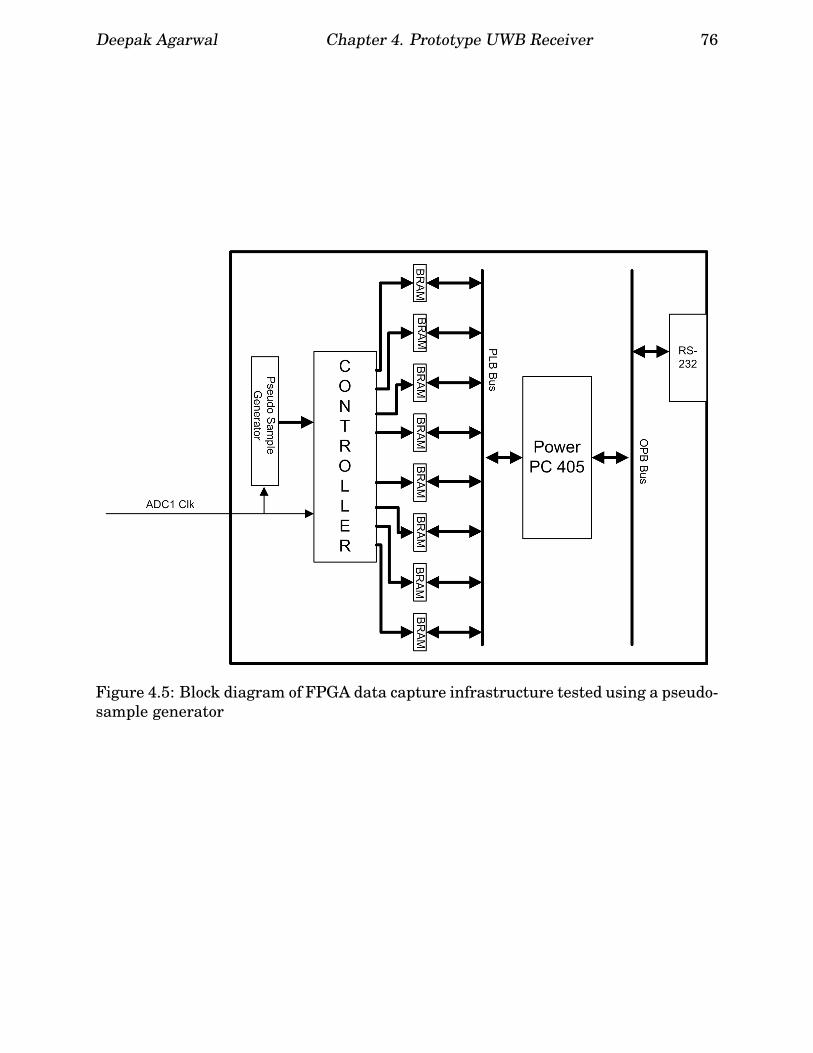
Deepak Agarwal Chapter 4. Prototype UWB Receiver 76
Figure 4.5: Block diagram of FPGA data capture infrastructure tested using a pseudo-
sample generator

Deepak Agarwal Chapter 4. Prototype UWB Receiver 77
Figure 4.6: Output from Minicom which verified that all FPGA data capture in-
frastructure was fully operational. Infrastructure was tested by inputting a pseudo-
sample sequence which is seen in the data stream above.

Deepak Agarwal Chapter 4. Prototype UWB Receiver 78
the PowerPC outputs the data to the host PC using the RS-232 interface. For initial
testing purposes, a 50Ω dummy load was connected to the UWB In input (J6) connec-
tor, to prevent accidentally overdriving the ADC analog input. The captured data was
output to the host PC and saved to a file. Test results show noisy data centered on
the midrange of the ADC’s output (output code 127), as seen in Figure 4.7.
4.4.5 DC Input Data Capture
DC voltages were connected to the prototype receiver PCB signal input (J6) to test
the following:
• ADC full-scale analog input range.
• Solder joint failures (leading to outputs that are stuck high or low).
• ADC DC Offset Calibration
ADC Analog Range
The ADC input was connected to a DC voltage source that was set equal to either the
maximum or minimum allowed analog input voltage (+250 mV for the maximum,
−250 mV for the minimum). The resulting output should have been either an all ‘1’s
code or an all ‘0’s code for their respective cases. During testing, it was observed that

Deepak Agarwal Chapter 4. Prototype UWB Receiver 79
(a) Output of ADC#1
(b) Output of ADC#2
Figure 4.7: Output of the ADCs when a 50Ω dummy load is connected to the UWB In
input. Note the slight gain and offset mismatch

Deepak Agarwal Chapter 4. Prototype UWB Receiver 80
the ADC overrange output was being asserted, meaning that the analog input was be-
ing overdriven. The overrange bit remained high until the input voltage was reduced
to ±63 mV, which was not the expected behavior for the ADC. After consulting with
MAX104 datasheets and Maxim application engineers, it was discovered that in the
prototype receiver’s design, the ADC’s internal bandgap reference pin, REFIN, was
inadvertently left floating. Not connecting the REFIN pin resulted in minimization of
the ADC analog input range; however, the functionality of the ADC remained essen-
tially unchanged. This problem could not be reworked on the PCB since the REFIN
pin was located such that it could not be accessed once the ADC had been soldered.
Solder Joint Failure
To test for solder joint failures, the ADC inputs were connected to a variable DC power
supply, and DC voltages were varied over the ADC’s input range (±63 mV). During
this test, it was observed that on Board #002, ADC #2’s output code always showed
noisy data and did not track the changing input. Further investigation revealed that
the analog input of ADC#2 was inoperative. On Board #001, several outputs on the
primary bus of ADC #002 were unresponsive to the changing DC input voltage. Close
inspection of the PCB revealed cold solder joints in the resistive voltage divider net-
work adjacent to the ADC. The solder joints were repaired and the ADC outputs were
observed to behave as expected.
Deepak Agarwal Chapter 4. Prototype UWB Receiver 81
ADC DC Offset Calibration
The MAX104 ADC’s provide a mechanism for matching the ADC offsets in a Time-
Interleaved Sampling array. On the prototype receiver, a variable resistor (R27 for
ADC#1 and R39 for ADC#2) are used to adjust the DC offset on the analog side of the
ADC. The MAX104 has an adjustment range of ±5.5 Least Significant Bits (LSBs).
Calibration involved inputting a fixed DC voltage and matching the ADC output codes
by adjusting the variable resistors.
4.4.6 Data Capture with Sinusoidal Input
Waveform Reconstruction from Individual ADCs
Each of the ADC’s output data is synchronous with their respective clock signals. In
the Time Interleaved Sampling architecture, the clock signals are intentionally out of
phase; hence, each ADC output must be latched into the FPGA using its respective
clock signal. Inside the FPGA, the single BRAM controller can be driven by either
of the ADC clock signals. To test the individual ADC data capture, two different bit-
streams were generated: one to read in data only from ADC#1 (as illustrated in Figure
4.8), and a second to read in data only from ADC#2 (Represented by the dotted line

Deepak Agarwal Chapter 4. Prototype UWB Receiver 82
Figure 4.8: Block diagram of FPGA data capture from individual ADCs
in Figure 4.8). Using separate bitstreams for each ADC avoided metastability issues
that would have occurred if the controller, running off ADC#1’s clock, attempted to
latch in data from ADC#2, or vice-versa. The individual ADC sampling clocks were
set to a frequency of 500 MHz, and a 12 MHz sinusoidal signal was input to the re-
ceiver’s UWB In input. The captured data was transmitted to the host PC and saved
to a file. The waveforms and their spectrums were reconstructed using a MATLAB
routine, and are shown in Figure 4.9.

Deepak Agarwal Chapter 4. Prototype UWB Receiver 83
(a) ADC#1 Time Domain Output (b) ADC#1 Frequency spectrum of cap-
tured samples
(c) ADC#2 Time Domain Output (d) ADC#2 Frequency spectrum of cap-
tured samples
Figure 4.9: Captured output from ADC#1 and ADC#2 for a 12 MHz CW input at a
sampling frequency of 500 MHz

Deepak Agarwal Chapter 4. Prototype UWB Receiver 84
Figure 4.10: Block diagram of FPGA data capture with ADC sample de-interleaving.
Waveform Reconstruction from Time Interleaved ADCs
As discussed above, metastability issues arise when the controller tries to read in
ADC#1’s output data when running on ADC#2’s clock. To avoid metastability, a syn-
chronizer is used to move data safely across clock domains, as illustrated in Figure
4.10.
A C routine written for the embedded PowerPC processor de-interleaves the data
while reading it from the BRAMs. To test the operation of the de-interleaving routine,

Deepak Agarwal Chapter 4. Prototype UWB Receiver 85
several Continuous Wave (CW) tones were input to the UWB In input of the receiver.
For the first round of testing, the individual ADC clocks were driven from an Agilent
ESG-D3000A signal generator at a frequency of 500 MHz. The programmable clock
delay chips for the ADCs were adjusted to provide an effective sampling frequency
of 1 GHz. The waveforms and their spectrums were reconstructed with a MATLAB
routine, and one example is plotted below in Figure 4.11. In the figures, note that
several spurious signals are present, the strongest of which occur at 250 MHz and at
fc − fin (where fc is the ADC clock signal and fin is the frequency of the input signal).
These spurs are caused by slightly mismatched delays, as well as clock jitter present
on the output of the Agilent signal generator. Nevertheless, the dynamic range of the
receiver is approximately 35 dB.
For the second round of testing, the individual ADC clocks were set to a frequency of
1 GHz, yielding an effective sampling frequency for the receiver of 2 GHz. As above,
several CW signals were input to the receiver, and one example of the resulting re-
constructed waveform and its spectrum is shown below in Figure 4.12. Note that the
dynamic range is approximately 38 dB, whereas the ideal dynamic range (if a single
2 GHz 8-bit ADC was used on the receiver) is 48 dB. The reduction in dynamic range
is primarily due to timing jitter (since the Agilent oscillator is somewhat noisy), but
is also due to minor gain and offset mismatches between the two ADCs.

Deepak Agarwal Chapter 4. Prototype UWB Receiver 86
(a) De-interleaved time domain output (b) Frequency spectrum of the De-
interleaved output
Figure 4.11: Time-Interleaved output of the prototype receiver PCB for a 127 MHz
CW input at an effective sampling frequency of 1 GHz.
(a) De-interleaved time domain output (b) Frequency spectrum of the De-
interleaved output
Figure 4.12: Time-Interleaved output of the prototype receiver PCB for a 151 MHz
CW input at an effective sampling frequency of 2 GHz.

Deepak Agarwal Chapter 4. Prototype UWB Receiver 87
4.4.7 Data Capture with a UWB Pulse Input
The final test of the prototype receiver board was to successfully capture and recon-
struct a UWB pulse generated by a MultiSpectral Solutions Inc. (MSSI) UWB pulser
available in the MPRG lab. To prevent overdriving the ADCs, the pulser output was
attenuated before connecting it the UWB In input of the prototype receiver. The
individual ADC clocks were set to a frequency of 1 GHz, yielding 2 GHz effective
sampling frequency for the receiver. Captured data was output to the host PC and
post-processed in Matlab as with the CW signals. For comparison purposes, the same
UWB pulse was also digitized using a Tektronix TDS580D at a 2 GHz sampling fre-
quency. The voltage recorded by the oscilloscope was converted into an equivalent
ADC output code level, based on the measured analog input range of the ADCs of 63
mV. Both signals are plotted together in Figure 4.13. Note that the two pulses are
nearly identical in both shape and time duration indicating a properly functioning
design.
4.4.8 Conclusions
The tests performed successfully demonstrated that all of the critical hardware com-
ponents on the prototype UWB software radio receiver are fully functional. Data
capture of both CW and UWB pulses was used to demonstrate that Time-Interleaved
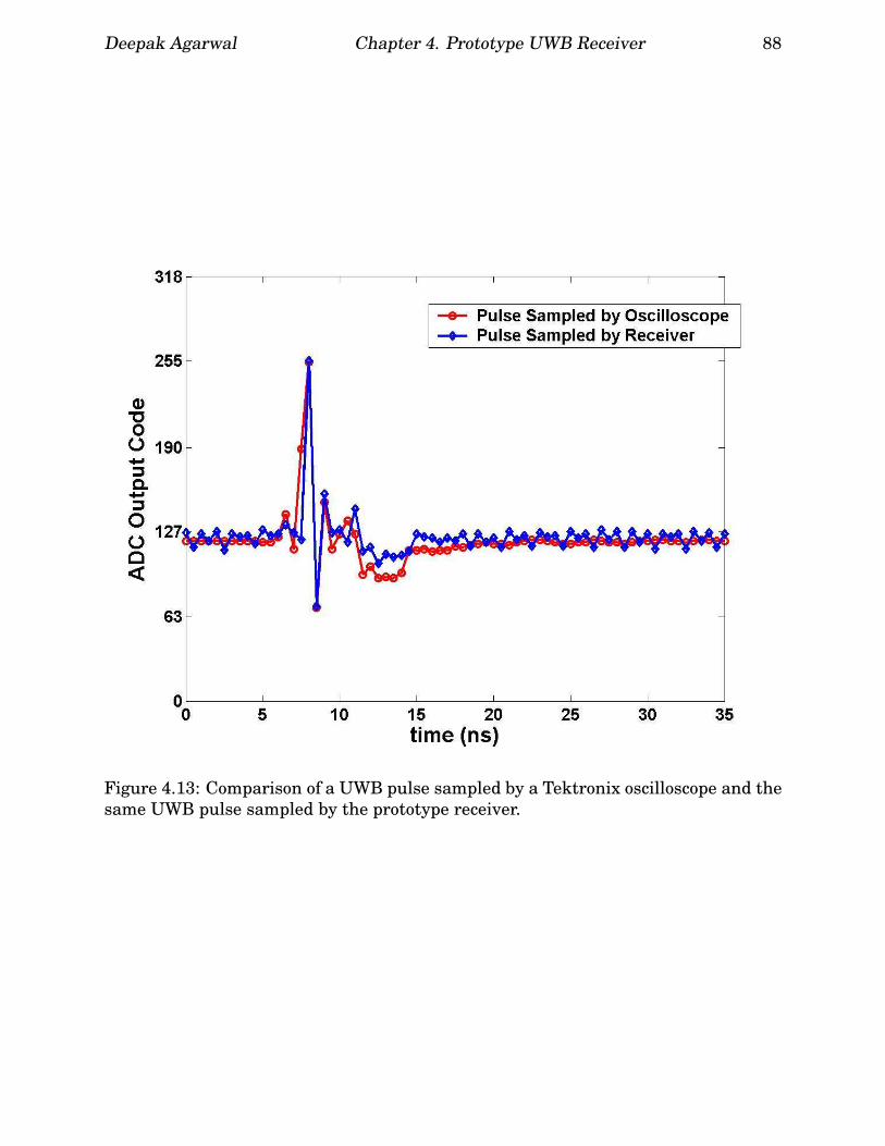
Deepak Agarwal Chapter 4. Prototype UWB Receiver 88
Figure 4.13: Comparison of a UWB pulse sampled by a Tektronix oscilloscope and the
same UWB pulse sampled by the prototype receiver.

Deepak Agarwal Chapter 4. Prototype UWB Receiver 89
sampling at such high frequencies and using off-the-shelf components is feasible. Ad-
ditionally, it was demonstrated that data paths inside the FPGA could operate at
clock frequencies of 250 MHz, which is critically important when the individual ADC
sampling clocks are set to 1 GHz.

Chapter 5
Conclusion and Future Work
This thesis detailed the design of the digital part of a impulse-based ultra wideband
testbed. The radio was based on software radio design concepts, and was built using
COTS-only components; hence, an FPGA was considered an optimal choice to imple-
ment the digital components of the communication system. Chapter 1 presented an
introduction to UWB communication systems and a discussion of its advantages over
traditional narrowband radios.
Chapter 2 provided the background information on software radios and an insight
into the trade-offs involved in selecting the underlying technology. The advantages
of using configurable computing devices like FPGAs, as compared to general purpose
microprocessors, DSPs or ASICs, for building software radios were highlighted. The
90

Deepak Agarwal Chapter 5. Conclusion and Future Work 91
research as well as commercial development of UWB systems has picked up steam
since FCC released the necessary bandwidth for UWB systems. A more in-depth dis-
cussion of UWB, along with a survey of state-of-the-art UWB systems was presented.
FPGAs, due to their flexibility, can be easily customized to implement optimal dat-
apath specific to an application. A number of high-speed datapath implementations
where FPGAs show a distinct performance advantage as compared to other architec-
tures, were discussed.
The Advanced UWB receiver board design was discussed in Chapter 3 with special
focus on the digital design. The receiver contained two critical parts; the Time-
Interleaved sampling implemented using high-performance ADCs and very low-skew
and low-jitter clock distribution system and a Xilinx Virtex-II Pro FPGA for baseband
processing. Time-Interleaved sampling is used to sample the incoming signal using a
bank of eight ADCs. The sampling scheme, limitations of COTS-based designs, ADC
and clock networks, acquisition and synchronization, demodulator design, real-time
tracking of the UWB pulse train and external interfaces were discussed. Some design
results were provided which illustrate that the proposed design is capable of running
at 250 MHz, which is essential to process the sample inputs in real-time.
The feasibilty of TI-Sampling scheme at high frequencies was demonstrated by build-
ing a proof-of-concept receiver. This prototype receiver is a scaled down version of the

Deepak Agarwal Chapter 5. Conclusion and Future Work 92
advanced UWB communication radio. It uses two ADCs, each sampling at 1 GHz,
to achieve an effective sampling rate of 2 GHz. To implement the digital part of the
receiver, a Xilinx Virtex-II Pro FPGA was chosen. Chapter 4 outlined the motivation
for fabricating this intermediate board and its design considerations, with emphasis
on digital design. The methodology for testing and evaluation of this board, the prob-
lems discovered during debugging, and some results were provided.
Chapter 5 gives a summary of the research efforts and discusses future research di-
rections in this area.
5.1 Future Work
This thesis has laid the groundwork for the digital designs needed for the advanced
UWB receiver, though it is yet to be fabricated. This leaves the door open for design
changes that can implement this baseband processor more efficiently by using fewer
FPGA resources. The high-speed FPGA design techniques used in this thesis are ex-
perimental and a more formal design methodology is desirable for implementing high
throughput dataflow architectures. On the prototype board, the deinterleaving of CW
tone and UWB waves was performed successfully at the rated sample clock frequency
of 1 GHz; however, it still needs to be ascertained that the acquisition and synchro-

Deepak Agarwal Chapter 5. Conclusion and Future Work 93
nization scheme proposed in this thesis will be able to lock the phase of receiver and
transmitter.
5.2 Conclusion
This thesis presented the design and implementation of the digital section of an
impulse-based software-defined UWB radio communication system. This communi-
cation system was designed to be used as a powerful, general purpose radio testbed.
Future students and researchers can use it for the evaluation of the impact of pulse
shaping, channel coding, error control, and network algorithms on UWB communi-
cation since the testbed is highly reconfigurable. In addition to communications, the
receiver can be used for propagation research, for Radar or imaging, or for more tra-
ditional narrowband/broadband communications.
As an intermediate step, a prototype SDR receiver, which is a scaled down version of
the advanced UWB system, was designed and fabricated. Successful deinterleaving
of CW tones and UWB pulse was performed at an effective sampling rate of 2 GHz. It
was demonstrated that TI-sampling based approach for wideband signals is feasible
using COTS components. Some valuable lessons were learned by discovering design
mistakes, which will now be rectified in the advanced receiver design.

Bibliography
1. A. M. Orndorff, “Transceiver design for ultra-wideband communications,” Mas-
ter’s thesis, Virginia Polytechnic Institute and State University, 2004.
2. C. R. Anderson, “A software radio defined ultra wideband transceiver transceiver
testbed for communication, ranging and imaging,” Ph.D. dissertation, Virginia
Polytechnic Institute and State University, to be published in 2006.
3. G. Ross, “The transient analysis of multiple beam feed networks for array sys-
tems,” Ph.D. dissertation, Polytechnic Institute of Brooklyn, 1963.
4. G. F. Ross, “Transmission and reception system for generating and receiving base-
band duration pulse signals without distortion for short base-band pulse commu-
nication system,” U.S. Patent, Tech. Rep. 3,728,632, April 7 1973.
5. F. C. Commission, “Revision of part 15 of the commissions rules regarding ultra-
wideband transmission systems, first note and order,” Federal Communications
Commission, Tech. Rep. ET-Docket 98-153, 2002, adopted February 14, 2002, re-
leased April 22, 2002.
94

Deepak Agarwal Bibliography 95
6. C. R. Anderson, A. Annamalai, A. M. Attiya, N. J. August, R. M. Buehrer, W. A.
Davis, M. X. Gong, S. Griggs, D. S. Ha, S. Licul, S. F. Midkiff, S. Muthuswamy, J. O.
Neel, J. H. Reed, S. Riad, B. M. Sadler, A. Safaai-Jazi, A. Swami, D. G. Sweeney,
and W. H. Tranter, An Introduction to Ultra Wideband Communications. Upper
Saddle River, NJ: Prentice Hall, 2005.
7. T. W. Barrett, “History of ultra wideband communications and radar: Part 2, uwb
radar and sensors,” Microwave Journal, pp. 22–46, February 2001.
8. L. Yang and G. B. Giannakis, “Ultra-wideband communications: an idea whose
time has come,” Signal Processing Magazine, IEEE, vol. 21, no. 6, pp. 26–54, 2004.
9. M. S. Gudaitis and R. D. Hinman, “Tactical software radio concept,” in Proceed-
ings MILCOM, Vol. 3, 1997.
10. “Software defined radio forum,” http://www.sdrforum.org.
11. J. H. Reed, Software Radio A Modern Approach to Radio Engineering. Upper
Saddle River, NJ: Prentice Hall, 2002.
12. “Joint tactical radio systems,” http://jtrs.army.mil.
13. P. M. Athanas, J. H. Reed, and W. H. Tranter, “A prototype software radio based
on configurable computing,” Advanced Microelectronics, pp. 34–39, 1998.
14. “Two flows for partial reconfiguration: Module based or difference based:
Xapp290,” Xilinx Inc.

Deepak Agarwal Bibliography 96
15. R. Mark, “Xtremespectrum rolls out first uwb chipset,”
http://www.ultrawidebandplanet.com/products/article.php/1370251.
16. P. Mannion, “Module makers take sides in bitter uwb battle,” 2004,
http://www.commsdesign.com/news/tech beat/showArticle.jhtml?articleID=46800057.
17. “Freescale semiconductors,” http://www.freescale.com.
18. R. J. Fontana, E. Richley, and J. Barney, “Commercialization of an ultra wideband
precision asset location system,” IEEE Conference on Ultra Wideband Systems
and Technologies, 2003, pp. 369–373, 2003.
19. R. Fontana, A. Ameti, E. Richley, L. Beard, and D. Guy, “Recent advances in ultra
wideband communications systems,” 2002 IEEE Conference on Ultra Wideband
Systems and Technologies, 2002. Digest of Papers., pp. 129–133, 2002.
20. M. I. Poygina, Z. F. Pasechnik, Y. Tsvirko, N. F. Karushkin, and S. B. Mal’tsev, “Re-
search institute orion has more that 40 years experience in the field of microwave
and millimeter-wave technology,” Microwave and Telecommunication Technology,
2003. CriMiCo 2003. 13th International Crimean Conference, pp. 814–820, 2003.
21. A. Ameti, R. J. Fontana, E. J. Knight, and E. Richley, “Ultra wideband technology
for aircraft wireless intercommunications systems (awics) design,” Aerospace and
Electronic Systems Magazine, IEEE, vol. 19, no. 7, pp. 14–18, 2004.

Deepak Agarwal Bibliography 97
22. H.-Y. Liao, M.-L. Yin, and Y. Cheng, “A parallel implementation of the smith-
waterman algorithm for massive sequences searching,” 26th Annual Interna-
tional Conference of the Engineering in Medicine and Biology Society, EMBC
2004., vol. 2, pp. 2817–2820 Vol.4, 2004.
23. D. J. Allred, W. Huang, V. Krishnan, H. Yoo, and D. V. Anderson, “An fpga im-
plementation for a high throughput adaptive filter using distributed arithmetic,”
12th Annual IEEE Symposium on Field-Programmable Custom Computing Ma-
chines, 2004. FCCM 2004, pp. 324–325, 2004.
24. C. Chad, Z. Qin, X. Yingke, and H. Chengde, “Design of a high performance fft
processor based on fpga,” Proceedings of the ASP-DAC 2005. Asia and South Pa-
cific Design Automation Conference, 2005., vol. 2, pp. 920–923 Vol. 2, 2005.
25. T. W. Nuteson, J. S. Clark, D. S. Haque, and G. S. Mitchell, “Digital beamforming
and calibration for smart antennas using real-time fpga processing,” IEEE MTT-S
International Microwave Symposium Digest, 2002, vol. 1, pp. 307–310, 2002.
26. R. Stapleton, K. Merranko, C. Parris, and J. Alter, “The use of field programmable
gate arrays in high performance radar signal processing applications,” The Record
of the IEEE 2000 International Radar Conference, 2000., pp. 850–855, 2000.
27. G. Lienhart, R. Lay, K. H. Noffz, and R. Manner, “An fpga-based video compressor
for h.263 compatible bitstreams,” International Conference on Consumer Electron-
ics, 2000. ICCE. 2000 Digest of Technical Papers, pp. 320–321, 2000.

Deepak Agarwal Bibliography 98
28. F. Rodriguez-Henriquez, N. A. Saqib, and A. Diaz-Perez, “4.2 gbit/s single-chip
fpga implementation of aes algorithm,” Electronics Letters, vol. 39, no. 15, pp.
1115–1116, 2003.
29. T. J. Todman, G. A. Constantinides, S. J. E. Wilton, O. Mencer, W. Luk, and P. Y. K.
Cheung, “Reconfigurable computing: architectures and design methods,” Comput-
ers and Digital Techniques, IEE Proceedings-, vol. 152, no. 2, pp. 193–207, 2005.
30. G. Danese, L. De Lotto, F. Leporati, M. Scaricabarozzi, and A. Spelgatti, “An accel-
erator for double precision floating point operations,” Proceedings. Eleventh Eu-
romicro Conference on Parallel, Distributed and Network-Based Processing, 2003.,
pp. 57–63, 2003.
31. MAXIM 104 : 5V, 1 Gsps, 8-bit ADC with On-Chip 2.2 GHz Track/Hold Amplifier,
MAXIM Integrated Products Inc. [Online]. Available: http://www.maxim-ic.com
32. Xilinx Virtex-II Pro and Virtex-II Pro X Platform FPGAs: Complete Data Sheet,
Xilinx Inc.
33. R. C. Dixon, Spread Spectrum Systems. New York: John Wiley and Sons Inc.,
1984.
34. J. Proakis, Digital Communication. McGraw-Hill Science/Engineering/Math,
2000.

Deepak Agarwal Bibliography 99
35. D. Agarwal, C. R. Anderson, and P. M. Athanas, “An 8 ghz ultra wideband
transceiver prototyping testbed,” in International Workshop on Rapid System Pro-
totyping, 2005.
36. Xilinx Platform Studio User Guide: Embedded Development Kit EDK 7.1i, Xilinx
Inc.
37. C. R. Anderson, D. Agarwal, J. H. Reed, and P. M. Athanas, “Test and evaluation
report for the prototype ultra wideband software defined radio receiver : Receiver
hardware,” Virginia Polytechnic Institute and State University, Tech. Rep., 2005.
38. “Configuration and readback of virtex fpgas using (jtag) boundary scan:
Xapp139,” Xilinx Inc.

Vita
Deepak Agarwal was born in Kanpur, India in 1977. He graduated with a Bachelor’s
degree in Electrical Engineering from Indian Institute of Technology, Kanpur in May
1999 and joined Texas Instruments (TI) India as an IC Design Engineer. At TI, he
was part of the team that successfully designed the “Mantra” C28X DSP core. In
2001, he joined Proceler Inc. Atlanta as a Senior Systems Engineer where he worked
on design problems related to reconfigurable computing. Following this, he decided
to continue his studies and enrolled as a Master’s student at Bradley’s Department
of Electrical Engineering at Virginia Polytechnic Institute and State University in
2003. At Virginia Tech, he was employed as a Graduate Research Assistant at the
Configurable Computing Lab, and completed his thesis under the guidance of Dr.
Peter M. Athanas. After graduating from Virginia Tech in 2005, he will commence
work at National Instruments in Austin, TX.
100