Embed Size (px)
Citation preview
DATA CONVERTER ARCHITECTURES
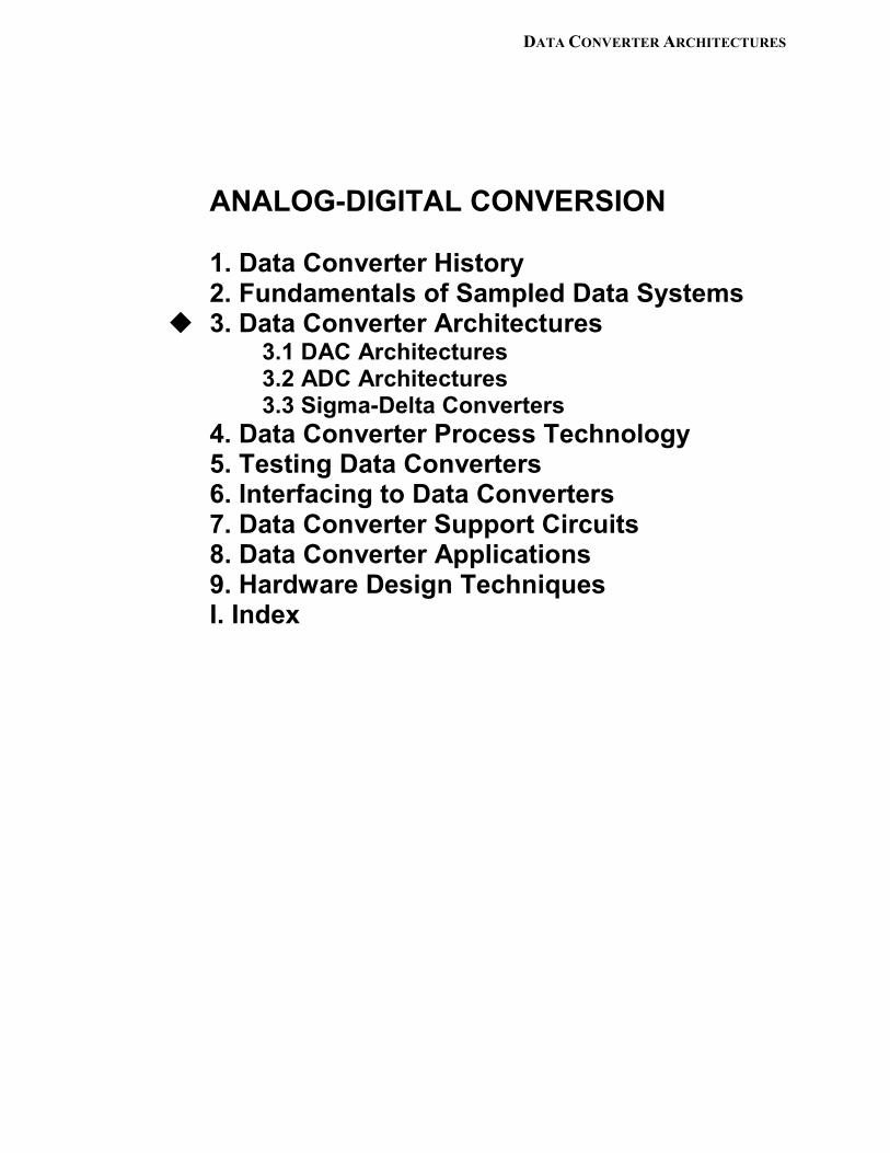
ANALOG-DIGITAL CONVERSION 1. Data Converter History 2. Fundamentals of Sampled Data Systems 3. Data Converter Architectures
3.1 DAC Architectures 3.2 ADC Architectures 3.3 Sigma-Delta Converters 4. Data Converter Process Technology 5. Testing Data Converters 6. Interfacing to Data Converters 7. Data Converter Support Circuits 8. Data Converter Applications 9. Hardware Design Techniques I. Index

ANALOG-DIGITAL CONVERSION
DATA CONVERTER ARCHITECTURES 3.1 DAC ARCHITECTURES
3.1
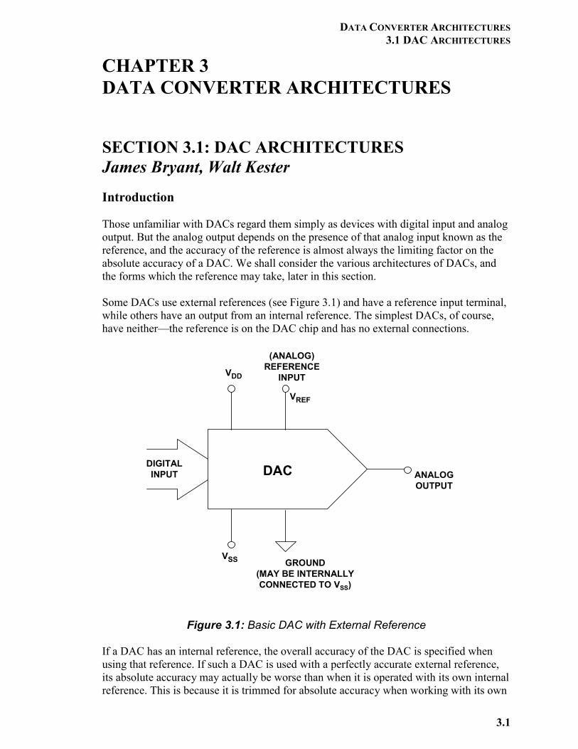
CHAPTER 3 DATA CONVERTER ARCHITECTURES SECTION 3.1: DAC ARCHITECTURES James Bryant, Walt Kester Introduction Those unfamiliar with DACs regard them simply as devices with digital input and analog output. But the analog output depends on the presence of that analog input known as the reference, and the accuracy of the reference is almost always the limiting factor on the absolute accuracy of a DAC. We shall consider the various architectures of DACs, and the forms which the reference may take, later in this section. Some DACs use external references (see Figure 3.1) and have a reference input terminal, while others have an output from an internal reference. The simplest DACs, of course, have neither—the reference is on the DAC chip and has no external connections.
Figure 3.1: Basic DAC with External Reference If a DAC has an internal reference, the overall accuracy of the DAC is specified when using that reference. If such a DAC is used with a perfectly accurate external reference, its absolute accuracy may actually be worse than when it is operated with its own internal reference. This is because it is trimmed for absolute accuracy when working with its own
DIGITALINPUT
VDD
VSS GROUND(MAY BE INTERNALLY CONNECTED TO VSS)
(ANALOG)REFERENCE
INPUT
DAC ANALOGOUTPUT
VREF
ANALOG-DIGITAL CONVERSION
3.2
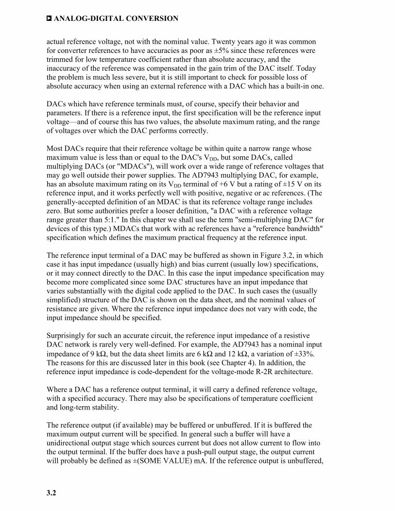
actual reference voltage, not with the nominal value. Twenty years ago it was common for converter references to have accuracies as poor as ±5% since these references were trimmed for low temperature coefficient rather than absolute accuracy, and the inaccuracy of the reference was compensated in the gain trim of the DAC itself. Today the problem is much less severe, but it is still important to check for possible loss of absolute accuracy when using an external reference with a DAC which has a built-in one. DACs which have reference terminals must, of course, specify their behavior and parameters. If there is a reference input, the first specification will be the reference input voltage—and of course this has two values, the absolute maximum rating, and the range of voltages over which the DAC performs correctly. Most DACs require that their reference voltage be within quite a narrow range whose maximum value is less than or equal to the DAC's VDD, but some DACs, called multiplying DACs (or "MDACs"), will work over a wide range of reference voltages that may go well outside their power supplies. The AD7943 multiplying DAC, for example, has an absolute maximum rating on its VDD terminal of +6 V but a rating of ±15 V on its reference input, and it works perfectly well with positive, negative or ac references. (The generally-accepted definition of an MDAC is that its reference voltage range includes zero. But some authorities prefer a looser definition, "a DAC with a reference voltage range greater than 5:1." In this chapter we shall use the term "semi-multiplying DAC" for devices of this type.) MDACs that work with ac references have a "reference bandwidth" specification which defines the maximum practical frequency at the reference input. The reference input terminal of a DAC may be buffered as shown in Figure 3.2, in which case it has input impedance (usually high) and bias current (usually low) specifications, or it may connect directly to the DAC. In this case the input impedance specification may become more complicated since some DAC structures have an input impedance that varies substantially with the digital code applied to the DAC. In such cases the (usually simplified) structure of the DAC is shown on the data sheet, and the nominal values of resistance are given. Where the reference input impedance does not vary with code, the input impedance should be specified. Surprisingly for such an accurate circuit, the reference input impedance of a resistive DAC network is rarely very well-defined. For example, the AD7943 has a nominal input impedance of 9 kΩ, but the data sheet limits are 6 kΩ and 12 kΩ, a variation of ±33%. The reasons for this are discussed later in this book (see Chapter 4). In addition, the reference input impedance is code-dependent for the voltage-mode R-2R architecture. Where a DAC has a reference output terminal, it will carry a defined reference voltage, with a specified accuracy. There may also be specifications of temperature coefficient and long-term stability. The reference output (if available) may be buffered or unbuffered. If it is buffered the maximum output current will be specified. In general such a buffer will have a unidirectional output stage which sources current but does not allow current to flow into the output terminal. If the buffer does have a push-pull output stage, the output current will probably be defined as ±(SOME VALUE) mA. If the reference output is unbuffered,
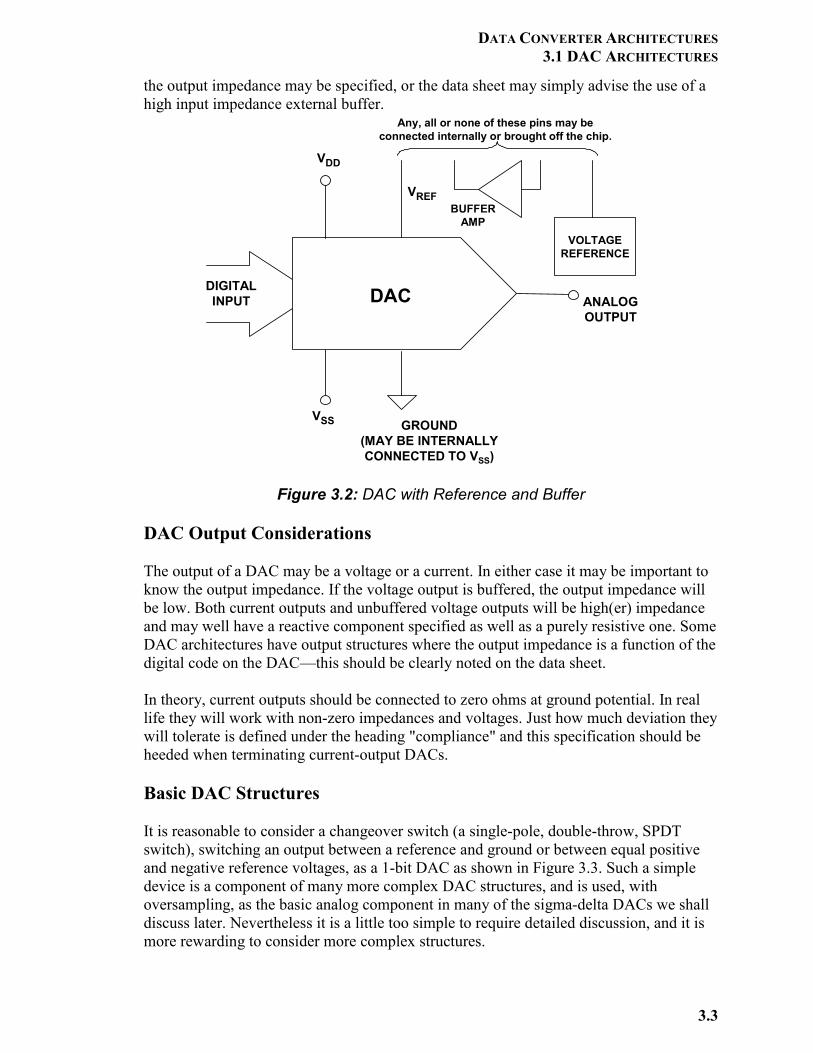
DATA CONVERTER ARCHITECTURES 3.1 DAC ARCHITECTURES
3.3
the output impedance may be specified, or the data sheet may simply advise the use of a high input impedance external buffer.
Figure 3.2: DAC with Reference and Buffer
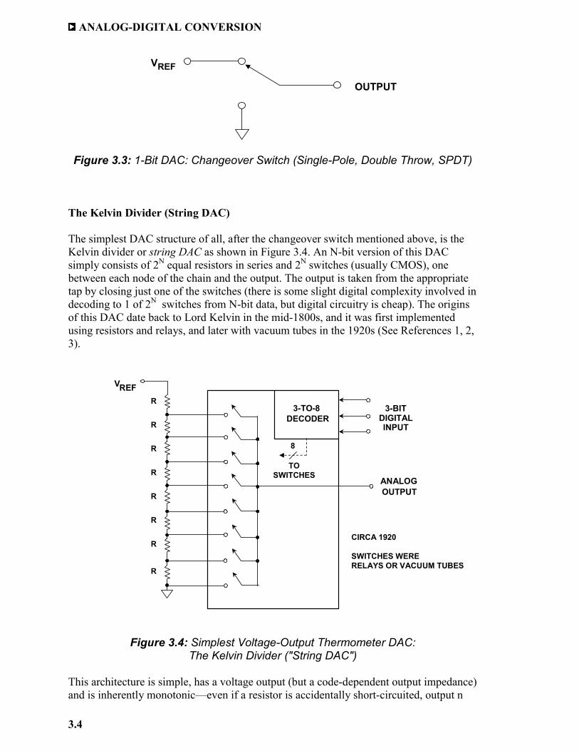
DAC Output Considerations The output of a DAC may be a voltage or a current. In either case it may be important to know the output impedance. If the voltage output is buffered, the output impedance will be low. Both current outputs and unbuffered voltage outputs will be high(er) impedance and may well have a reactive component specified as well as a purely resistive one. Some DAC architectures have output structures where the output impedance is a function of the digital code on the DAC—this should be clearly noted on the data sheet. In theory, current outputs should be connected to zero ohms at ground potential. In real life they will work with non-zero impedances and voltages. Just how much deviation they will tolerate is defined under the heading "compliance" and this specification should be heeded when terminating current-output DACs. Basic DAC Structures It is reasonable to consider a changeover switch (a single-pole, double-throw, SPDT switch), switching an output between a reference and ground or between equal positive and negative reference voltages, as a 1-bit DAC as shown in Figure 3.3. Such a simple device is a component of many more complex DAC structures, and is used, with oversampling, as the basic analog component in many of the sigma-delta DACs we shall discuss later. Nevertheless it is a little too simple to require detailed discussion, and it is more rewarding to consider more complex structures.
DIGITALINPUT
VDD
VSS GROUND(MAY BE INTERNALLY CONNECTED TO VSS)
DAC ANALOGOUTPUT
VREF
VOLTAGEREFERENCE
Any, all or none of these pins may beconnected internally or brought off the chip.
BUFFERAMP
ANALOG-DIGITAL CONVERSION
3.4
Figure 3.3: 1-Bit DAC: Changeover Switch (Single-Pole, Double Throw, SPDT)
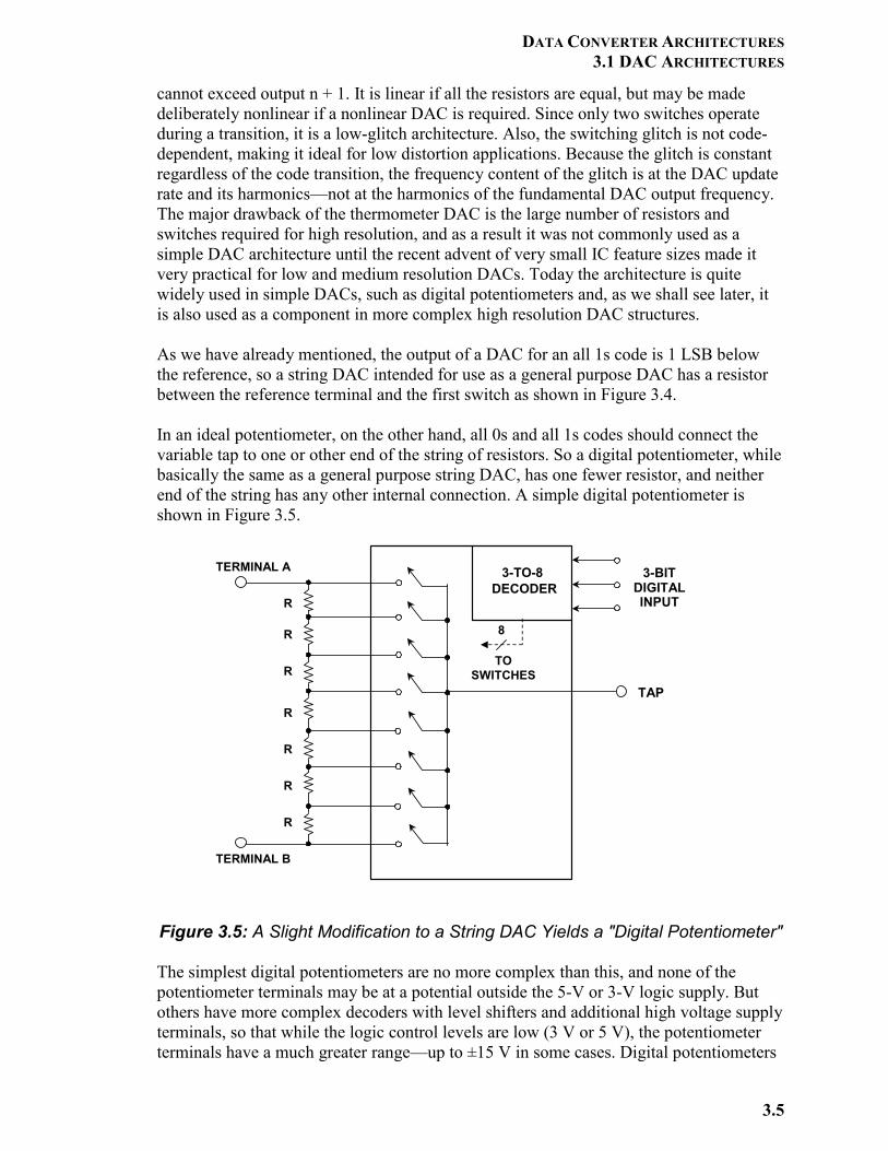
The Kelvin Divider (String DAC) The simplest DAC structure of all, after the changeover switch mentioned above, is the Kelvin divider or string DAC as shown in Figure 3.4. An N-bit version of this DAC simply consists of 2N equal resistors in series and 2N switches (usually CMOS), one between each node of the chain and the output. The output is taken from the appropriate tap by closing just one of the switches (there is some slight digital complexity involved in decoding to 1 of 2N switches from N-bit data, but digital circuitry is cheap). The origins of this DAC date back to Lord Kelvin in the mid-1800s, and it was first implemented using resistors and relays, and later with vacuum tubes in the 1920s (See References 1, 2, 3).
Figure 3.4: Simplest Voltage-Output Thermometer DAC: The Kelvin Divider ("String DAC")
This architecture is simple, has a voltage output (but a code-dependent output impedance) and is inherently monotonic—even if a resistor is accidentally short-circuited, output n
VREF
OUTPUT
3-TO-8DECODER
3-BITDIGITALINPUT
ANALOGOUTPUT
VREF
CIRCA 1920
SWITCHES WERERELAYS OR VACUUM TUBES
8
TOSWITCHES
R
R
R
R
R
R
R
R
DATA CONVERTER ARCHITECTURES 3.1 DAC ARCHITECTURES
3.5
cannot exceed output n + 1. It is linear if all the resistors are equal, but may be made deliberately nonlinear if a nonlinear DAC is required. Since only two switches operate during a transition, it is a low-glitch architecture. Also, the switching glitch is not code-dependent, making it ideal for low distortion applications. Because the glitch is constant regardless of the code transition, the frequency content of the glitch is at the DAC update rate and its harmonics—not at the harmonics of the fundamental DAC output frequency. The major drawback of the thermometer DAC is the large number of resistors and switches required for high resolution, and as a result it was not commonly used as a simple DAC architecture until the recent advent of very small IC feature sizes made it very practical for low and medium resolution DACs. Today the architecture is quite widely used in simple DACs, such as digital potentiometers and, as we shall see later, it is also used as a component in more complex high resolution DAC structures. As we have already mentioned, the output of a DAC for an all 1s code is 1 LSB below the reference, so a string DAC intended for use as a general purpose DAC has a resistor between the reference terminal and the first switch as shown in Figure 3.4. In an ideal potentiometer, on the other hand, all 0s and all 1s codes should connect the variable tap to one or other end of the string of resistors. So a digital potentiometer, while basically the same as a general purpose string DAC, has one fewer resistor, and neither end of the string has any other internal connection. A simple digital potentiometer is shown in Figure 3.5.
Figure 3.5: A Slight Modification to a String DAC Yields a "Digital Potentiometer" The simplest digital potentiometers are no more complex than this, and none of the potentiometer terminals may be at a potential outside the 5-V or 3-V logic supply. But others have more complex decoders with level shifters and additional high voltage supply terminals, so that while the logic control levels are low (3 V or 5 V), the potentiometer terminals have a much greater range—up to ±15 V in some cases. Digital potentiometers
3-TO-8DECODER
3-BITDIGITALINPUT
TAP
8
TOSWITCHES
R
R
R
R
R
R
R
TERMINAL A
TERMINAL B
ANALOG-DIGITAL CONVERSION
3.6
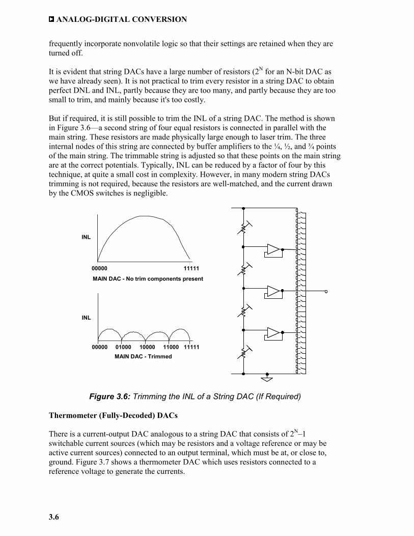
frequently incorporate nonvolatile logic so that their settings are retained when they are turned off. It is evident that string DACs have a large number of resistors (2N for an N-bit DAC as we have already seen). It is not practical to trim every resistor in a string DAC to obtain perfect DNL and INL, partly because they are too many, and partly because they are too small to trim, and mainly because it's too costly. But if required, it is still possible to trim the INL of a string DAC. The method is shown in Figure 3.6—a second string of four equal resistors is connected in parallel with the main string. These resistors are made physically large enough to laser trim. The three internal nodes of this string are connected by buffer amplifiers to the ¼, ½, and ¾ points of the main string. The trimmable string is adjusted so that these points on the main string are at the correct potentials. Typically, INL can be reduced by a factor of four by this technique, at quite a small cost in complexity. However, in many modern string DACs trimming is not required, because the resistors are well-matched, and the current drawn by the CMOS switches is negligible.
Figure 3.6: Trimming the INL of a String DAC (If Required)
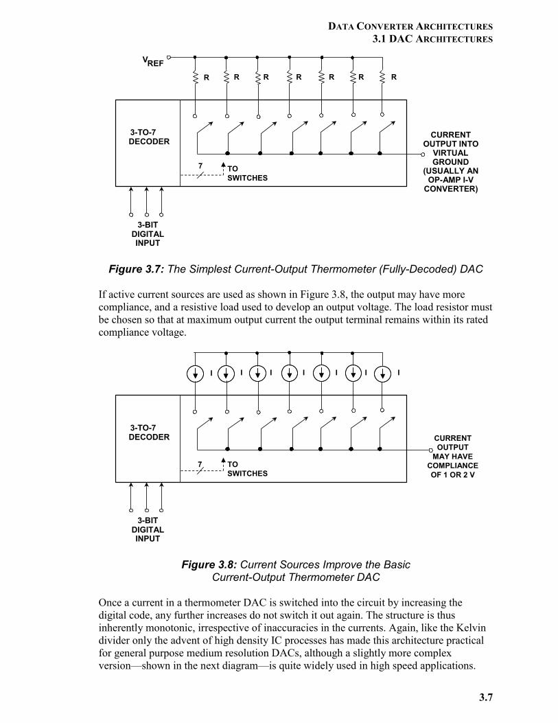
Thermometer (Fully-Decoded) DACs There is a current-output DAC analogous to a string DAC that consists of 2N–1 switchable current sources (which may be resistors and a voltage reference or may be active current sources) connected to an output terminal, which must be at, or close to, ground. Figure 3.7 shows a thermometer DAC which uses resistors connected to a reference voltage to generate the currents.
00000 11111
MAIN DAC - No trim components present
00000 11111
INL
INL
01000 1100010000MAIN DAC - Trimmed
DATA CONVERTER ARCHITECTURES 3.1 DAC ARCHITECTURES
3.7
Figure 3.7: The Simplest Current-Output Thermometer (Fully-Decoded) DAC
If active current sources are used as shown in Figure 3.8, the output may have more compliance, and a resistive load used to develop an output voltage. The load resistor must be chosen so that at maximum output current the output terminal remains within its rated compliance voltage.
Figure 3.8: Current Sources Improve the Basic
Current-Output Thermometer DAC Once a current in a thermometer DAC is switched into the circuit by increasing the digital code, any further increases do not switch it out again. The structure is thus inherently monotonic, irrespective of inaccuracies in the currents. Again, like the Kelvin divider only the advent of high density IC processes has made this architecture practical for general purpose medium resolution DACs, although a slightly more complex version—shown in the next diagram—is quite widely used in high speed applications.
3-BITDIGITALINPUT
CURRENTOUTPUT INTO
VIRTUALGROUND
(USUALLY ANOP-AMP I-V
CONVERTER)
VREF
3-TO-7DECODER
R R R R R R R
TOSWITCHES
7
3-BITDIGITALINPUT
3-TO-7DECODER
I I I I I I I
CURRENTOUTPUT
MAY HAVECOMPLIANCEOF 1 OR 2 V
TOSWITCHES
7
ANALOG-DIGITAL CONVERSION
3.8
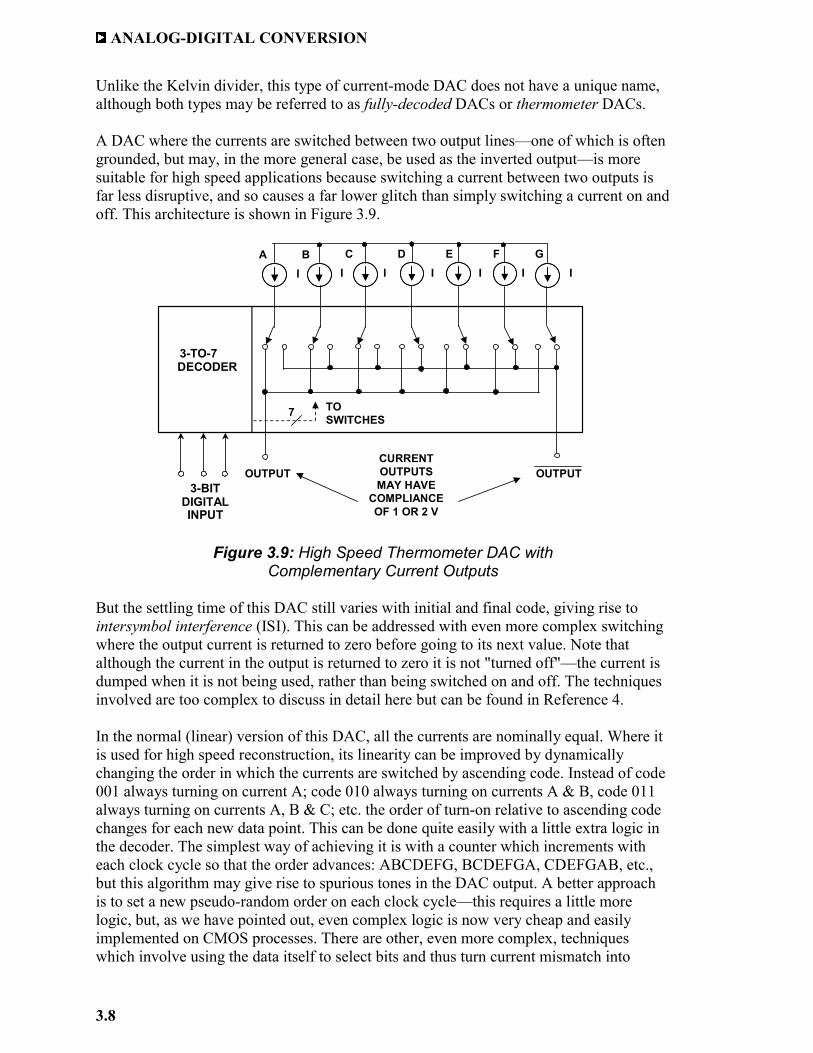
Unlike the Kelvin divider, this type of current-mode DAC does not have a unique name, although both types may be referred to as fully-decoded DACs or thermometer DACs. A DAC where the currents are switched between two output lines—one of which is often grounded, but may, in the more general case, be used as the inverted output—is more suitable for high speed applications because switching a current between two outputs is far less disruptive, and so causes a far lower glitch than simply switching a current on and off. This architecture is shown in Figure 3.9.
Figure 3.9: High Speed Thermometer DAC with
Complementary Current Outputs But the settling time of this DAC still varies with initial and final code, giving rise to intersymbol interference (ISI). This can be addressed with even more complex switching where the output current is returned to zero before going to its next value. Note that although the current in the output is returned to zero it is not "turned off"—the current is dumped when it is not being used, rather than being switched on and off. The techniques involved are too complex to discuss in detail here but can be found in Reference 4. In the normal (linear) version of this DAC, all the currents are nominally equal. Where it is used for high speed reconstruction, its linearity can be improved by dynamically changing the order in which the currents are switched by ascending code. Instead of code 001 always turning on current A; code 010 always turning on currents A & B, code 011 always turning on currents A, B & C; etc. the order of turn-on relative to ascending code changes for each new data point. This can be done quite easily with a little extra logic in the decoder. The simplest way of achieving it is with a counter which increments with each clock cycle so that the order advances: ABCDEFG, BCDEFGA, CDEFGAB, etc., but this algorithm may give rise to spurious tones in the DAC output. A better approach is to set a new pseudo-random order on each clock cycle—this requires a little more logic, but, as we have pointed out, even complex logic is now very cheap and easily implemented on CMOS processes. There are other, even more complex, techniques which involve using the data itself to select bits and thus turn current mismatch into
3-BITDIGITALINPUT
3-TO-7DECODER
I I I I I I I
CURRENTOUTPUTSMAY HAVE
COMPLIANCEOF 1 OR 2 V
OUTPUT OUTPUT
A B C D E F G
TOSWITCHES
7
DATA CONVERTER ARCHITECTURES 3.1 DAC ARCHITECTURES
3.9
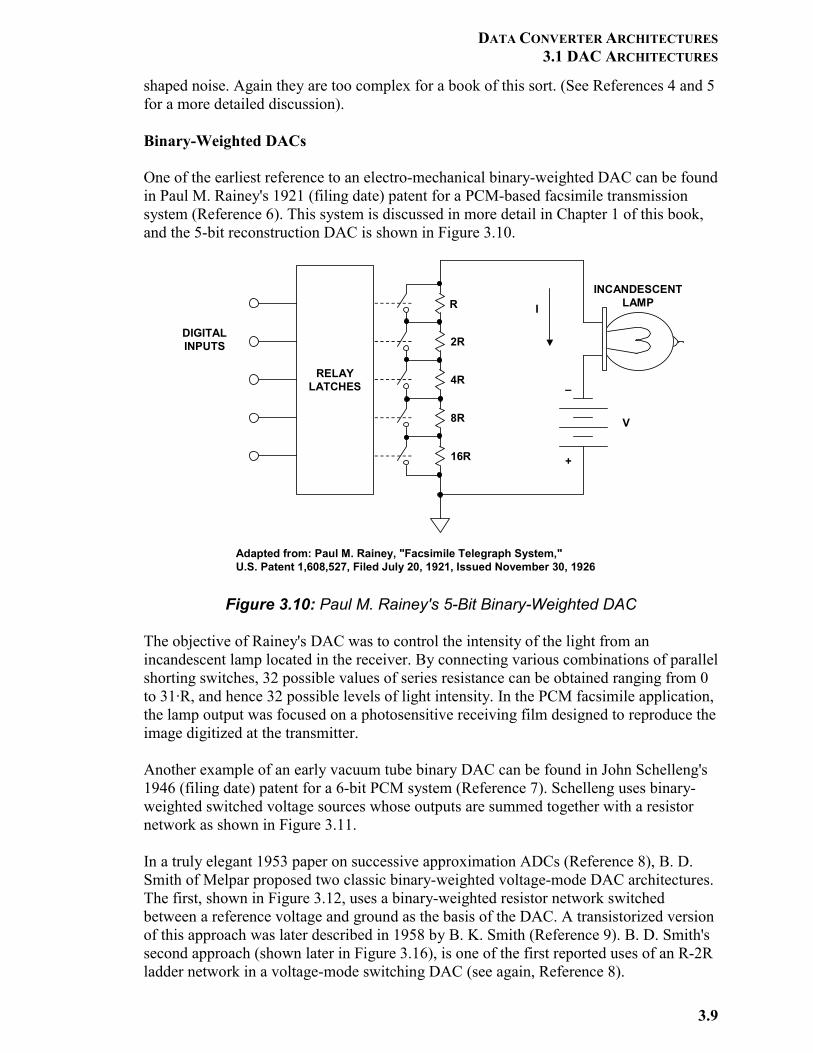
shaped noise. Again they are too complex for a book of this sort. (See References 4 and 5 for a more detailed discussion). Binary-Weighted DACs One of the earliest reference to an electro-mechanical binary-weighted DAC can be found in Paul M. Rainey's 1921 (filing date) patent for a PCM-based facsimile transmission system (Reference 6). This system is discussed in more detail in Chapter 1 of this book, and the 5-bit reconstruction DAC is shown in Figure 3.10.
Figure 3.10: Paul M. Rainey's 5-Bit Binary-Weighted DAC
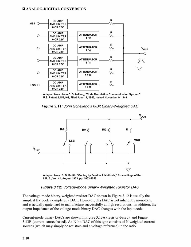
The objective of Rainey's DAC was to control the intensity of the light from an incandescent lamp located in the receiver. By connecting various combinations of parallel shorting switches, 32 possible values of series resistance can be obtained ranging from 0 to 31·R, and hence 32 possible levels of light intensity. In the PCM facsimile application, the lamp output was focused on a photosensitive receiving film designed to reproduce the image digitized at the transmitter. Another example of an early vacuum tube binary DAC can be found in John Schelleng's 1946 (filing date) patent for a 6-bit PCM system (Reference 7). Schelleng uses binary-weighted switched voltage sources whose outputs are summed together with a resistor network as shown in Figure 3.11. In a truly elegant 1953 paper on successive approximation ADCs (Reference 8), B. D. Smith of Melpar proposed two classic binary-weighted voltage-mode DAC architectures. The first, shown in Figure 3.12, uses a binary-weighted resistor network switched between a reference voltage and ground as the basis of the DAC. A transistorized version of this approach was later described in 1958 by B. K. Smith (Reference 9). B. D. Smith's second approach (shown later in Figure 3.16), is one of the first reported uses of an R-2R ladder network in a voltage-mode switching DAC (see again, Reference 8).
RELAYLATCHES
R
2R
4R
8R
16R
I
+
V
DIGITALINPUTS
INCANDESCENTLAMP
Adapted from: Paul M. Rainey, "Facsimile Telegraph System," U.S. Patent 1,608,527, Filed July 20, 1921, Issued November 30, 1926
–
ANALOG-DIGITAL CONVERSION
3.10
Figure 3.11: John Schelleng's 6-Bit Binary-Weighted DAC
Figure 3.12: Voltage-mode Binary-Weighted Resistor DAC
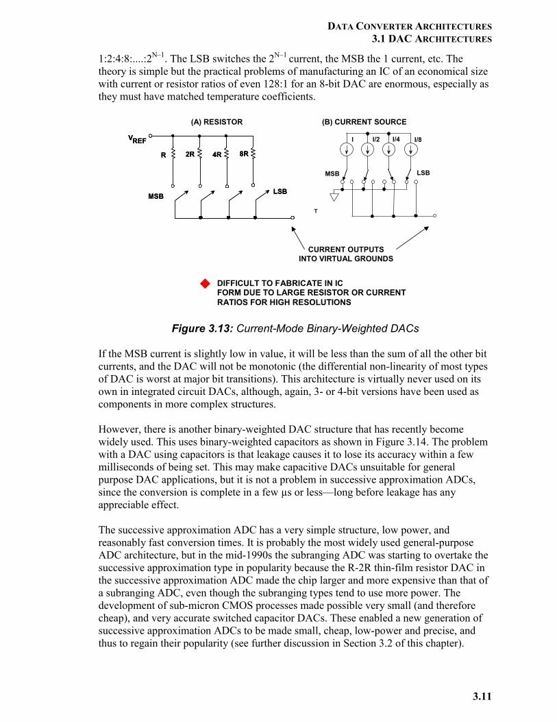
The voltage-mode binary-weighted resistor DAC shown in Figure 3.12 is usually the simplest textbook example of a DAC. However, this DAC is not inherently monotonic and is actually quite hard to manufacture successfully at high resolutions. In addition, the output impedance of the voltage-mode binary DAC changes with the input code. Current-mode binary DACs are shown in Figure 3.13A (resistor-based), and Figure 3.13B (current-source based). An N-bit DAC of this type consists of N weighted current sources (which may simply be resistors and a voltage reference) in the ratio
DC AMPAND LIMITER
0 OR 32V
ATTENUATOR1 / 2
DC AMPAND LIMITER
0 OR 32V
DC AMPAND LIMITER
0 OR 32V
DC AMPAND LIMITER
0 OR 32V
DC AMPAND LIMITER
0 OR 32V
DC AMPAND LIMITER
0 OR 32V
ATTENUATOR1 / 4
ATTENUATOR1 / 8
ATTENUATOR1 / 16
ATTENUATOR1 / 32
R
R
R
R
R
R
RL
Adapted from: John C. Schelleng, "Code Modulation Communication System,"U.S. Patent 2,453,461, Filed June 19, 1946, Issued November 9, 1948
MSB
LSB
VOUT
R/8 R/4 R/2 R
V
V
REF
OUT
MSBLSB
Adapted from: B. D. Smith, "Coding by Feedback Methods," Proceedings of the I. R. E., Vol. 41, August 1953, pp. 1053-1058
DATA CONVERTER ARCHITECTURES 3.1 DAC ARCHITECTURES
3.11
1:2:4:8:....:2N–1. The LSB switches the 2N–1 current, the MSB the 1 current, etc. The theory is simple but the practical problems of manufacturing an IC of an economical size with current or resistor ratios of even 128:1 for an 8-bit DAC are enormous, especially as they must have matched temperature coefficients.
Figure 3.13: Current-Mode Binary-Weighted DACs
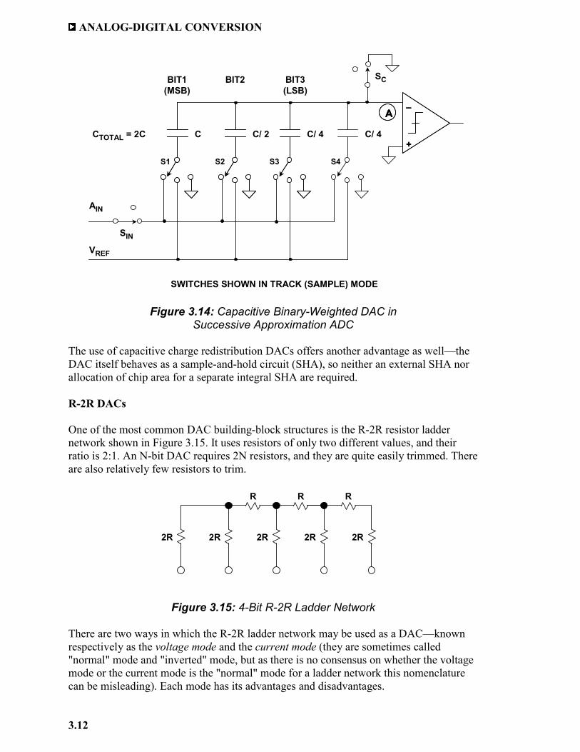
If the MSB current is slightly low in value, it will be less than the sum of all the other bit currents, and the DAC will not be monotonic (the differential non-linearity of most types of DAC is worst at major bit transitions). This architecture is virtually never used on its own in integrated circuit DACs, although, again, 3- or 4-bit versions have been used as components in more complex structures. However, there is another binary-weighted DAC structure that has recently become widely used. This uses binary-weighted capacitors as shown in Figure 3.14. The problem with a DAC using capacitors is that leakage causes it to lose its accuracy within a few milliseconds of being set. This may make capacitive DACs unsuitable for general purpose DAC applications, but it is not a problem in successive approximation ADCs, since the conversion is complete in a few µs or less—long before leakage has any appreciable effect. The successive approximation ADC has a very simple structure, low power, and reasonably fast conversion times. It is probably the most widely used general-purpose ADC architecture, but in the mid-1990s the subranging ADC was starting to overtake the successive approximation type in popularity because the R-2R thin-film resistor DAC in the successive approximation ADC made the chip larger and more expensive than that of a subranging ADC, even though the subranging types tend to use more power. The development of sub-micron CMOS processes made possible very small (and therefore cheap), and very accurate switched capacitor DACs. These enabled a new generation of successive approximation ADCs to be made small, cheap, low-power and precise, and thus to regain their popularity (see further discussion in Section 3.2 of this chapter).
DIFFICULT TO FABRICATE IN ICFORM DUE TO LARGE RESISTOR OR CURRENT RATIOS FOR HIGH RESOLUTIONS
VREF
MSB LSB
R 2R 4R 8R
VREF
MSB LSB
R 2R 4R 8R
CURRENT OUTPUTSINTO VIRTUAL GROUNDS
(A) RESISTOR (B) CURRENT SOURCE
T
I/2 I/4 I/8
LSBMSB
I
ANALOG-DIGITAL CONVERSION
3.12
Figure 3.14: Capacitive Binary-Weighted DAC in
Successive Approximation ADC The use of capacitive charge redistribution DACs offers another advantage as well—the DAC itself behaves as a sample-and-hold circuit (SHA), so neither an external SHA nor allocation of chip area for a separate integral SHA are required. R-2R DACs One of the most common DAC building-block structures is the R-2R resistor ladder network shown in Figure 3.15. It uses resistors of only two different values, and their ratio is 2:1. An N-bit DAC requires 2N resistors, and they are quite easily trimmed. There are also relatively few resistors to trim.
Figure 3.15: 4-Bit R-2R Ladder Network There are two ways in which the R-2R ladder network may be used as a DAC—known respectively as the voltage mode and the current mode (they are sometimes called "normal" mode and "inverted" mode, but as there is no consensus on whether the voltage mode or the current mode is the "normal" mode for a ladder network this nomenclature can be misleading). Each mode has its advantages and disadvantages.
_
+
_
+C/ 4C/ 2C C/ 4
AIN
VREF
SIN
SC
S1 S2 S3 S4
BIT1(MSB)
BIT2 BIT3(LSB)
SWITCHES SHOWN IN TRACK (SAMPLE) MODE
AA
CTOTAL = 2C
2R 2R 2R 2R 2R
R R R
DATA CONVERTER ARCHITECTURES 3.1 DAC ARCHITECTURES
3.13
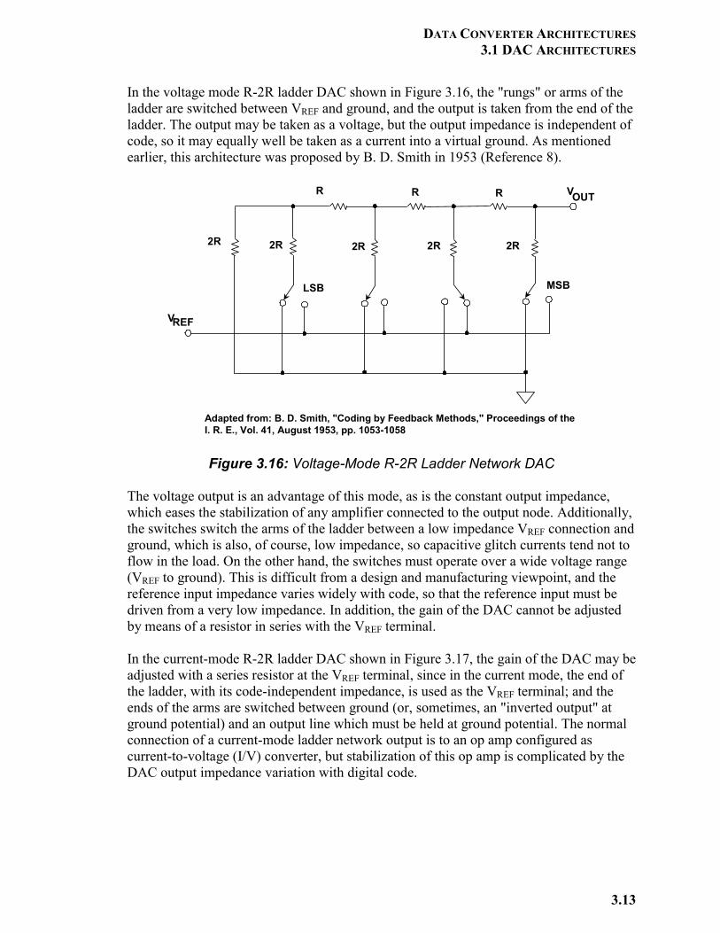
In the voltage mode R-2R ladder DAC shown in Figure 3.16, the "rungs" or arms of the ladder are switched between VREF and ground, and the output is taken from the end of the ladder. The output may be taken as a voltage, but the output impedance is independent of code, so it may equally well be taken as a current into a virtual ground. As mentioned earlier, this architecture was proposed by B. D. Smith in 1953 (Reference 8).
Figure 3.16: Voltage-Mode R-2R Ladder Network DAC
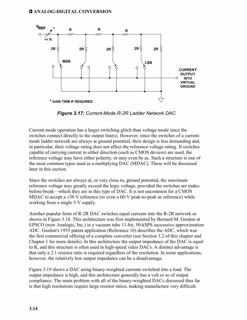
The voltage output is an advantage of this mode, as is the constant output impedance, which eases the stabilization of any amplifier connected to the output node. Additionally, the switches switch the arms of the ladder between a low impedance VREF connection and ground, which is also, of course, low impedance, so capacitive glitch currents tend not to flow in the load. On the other hand, the switches must operate over a wide voltage range (VREF to ground). This is difficult from a design and manufacturing viewpoint, and the reference input impedance varies widely with code, so that the reference input must be driven from a very low impedance. In addition, the gain of the DAC cannot be adjusted by means of a resistor in series with the VREF terminal. In the current-mode R-2R ladder DAC shown in Figure 3.17, the gain of the DAC may be adjusted with a series resistor at the VREF terminal, since in the current mode, the end of the ladder, with its code-independent impedance, is used as the VREF terminal; and the ends of the arms are switched between ground (or, sometimes, an "inverted output" at ground potential) and an output line which must be held at ground potential. The normal connection of a current-mode ladder network output is to an op amp configured as current-to-voltage (I/V) converter, but stabilization of this op amp is complicated by the DAC output impedance variation with digital code.
2R
R R R
2R 2R 2R 2R
V
V
REF
OUT
MSBLSB
Adapted from: B. D. Smith, "Coding by Feedback Methods," Proceedings of the I. R. E., Vol. 41, August 1953, pp. 1053-1058
ANALOG-DIGITAL CONVERSION
3.14
Figure 3.17: Current-Mode R-2R Ladder Network DAC
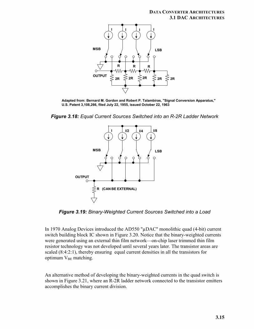
Current-mode operation has a larger switching glitch than voltage mode since the switches connect directly to the output line(s). However, since the switches of a current-mode ladder network are always at ground potential, their design is less demanding and, in particular, their voltage rating does not affect the reference voltage rating. If switches capable of carrying current in either direction (such as CMOS devices) are used, the reference voltage may have either polarity, or may even be ac. Such a structure is one of the most common types used as a multiplying DAC (MDAC). These will be discussed later in this section. Since the switches are always at, or very close to, ground potential, the maximum reference voltage may greatly exceed the logic voltage, provided the switches are make-before-break—which they are in this type of DAC. It is not uncommon for a CMOS MDAC to accept a ±30 V reference (or even a 60-V peak-to-peak ac reference) while working from a single 5-V supply. Another popular form of R-2R DAC switches equal currents into the R-2R network as shown in Figure 3.18. This architecture was first implemented by Bernard M. Gordon at EPSCO (now Analogic, Inc.) in a vacuum tube 11-bit, 50-kSPS successive approximation ADC. Gordon's 1955 patent application (Reference 10) describes the ADC, which was the first commercial offering of a complete converter (see Section 3.2 of this chapter and Chapter 1 for more details). In this architecture the output impedance of the DAC is equal to R, and this structure is often used in high-speed video DACs. A distinct advantage is that only a 2:1 resistor ratio is required regardless of the resolution. In some applications, however, the relatively low output impedance can be a disadvantage. Figure 3.19 shows a DAC using binary-weighted currents switched into a load. The output impedance is high, and this architecture generally has a volt or so of output compliance. The main problem with all of the binary-weighted DACs discussed thus far is that high resolutions require large resistor ratios, making manufacture very difficult.
2R
RRR
2R2R2R2R
VREFVREF
MSB LSB
CURRENTOUTPUT
INTOVIRTUALGROUND
<< R
*
* GAIN TRIM IF REQUIRED
DATA CONVERTER ARCHITECTURES 3.1 DAC ARCHITECTURES
3.15
Figure 3.18: Equal Current Sources Switched into an R-2R Ladder Network
Figure 3.19: Binary-Weighted Current Sources Switched into a Load
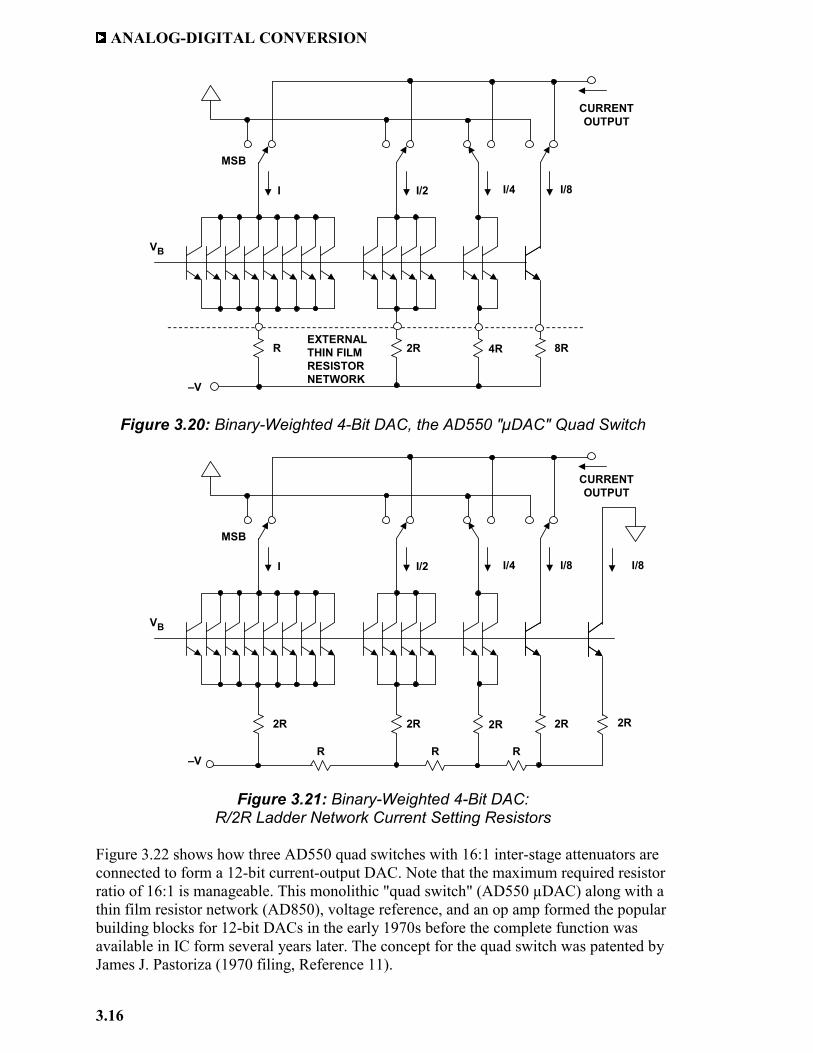
In 1970 Analog Devices introduced the AD550 "µDAC" monolithic quad (4-bit) current switch building block IC shown in Figure 3.20. Notice that the binary-weighted currents were generated using an external thin film network—on-chip laser trimmed thin film resistor technology was not developed until several years later. The transistor areas are scaled (8:4:2:1), thereby ensuring equal current densities in all the transistors for optimum VBE matching.
An alternative method of developing the binary-weighted currents in the quad switch is shown in Figure 3.21, where an R-2R ladder network connected to the transistor emitters accomplishes the binary current division.
I I I I
OUTPUT
MSB
R R R
2R 2R 2R
Adapted from: Bernard M. Gordon and Robert P. Talambiras, "Signal Conversion Apparatus,"U.S. Patent 3,108,266, filed July 22, 1955, issued October 22, 1963
2R2R
LSB
R (CAN BE EXTERNAL)
OUTPUT
I I/2 I/4 I/8
MSB LSB
ANALOG-DIGITAL CONVERSION
3.16
Figure 3.20: Binary-Weighted 4-Bit DAC, the AD550 "µDAC" Quad Switch
Figure 3.21: Binary-Weighted 4-Bit DAC:
R/2R Ladder Network Current Setting Resistors
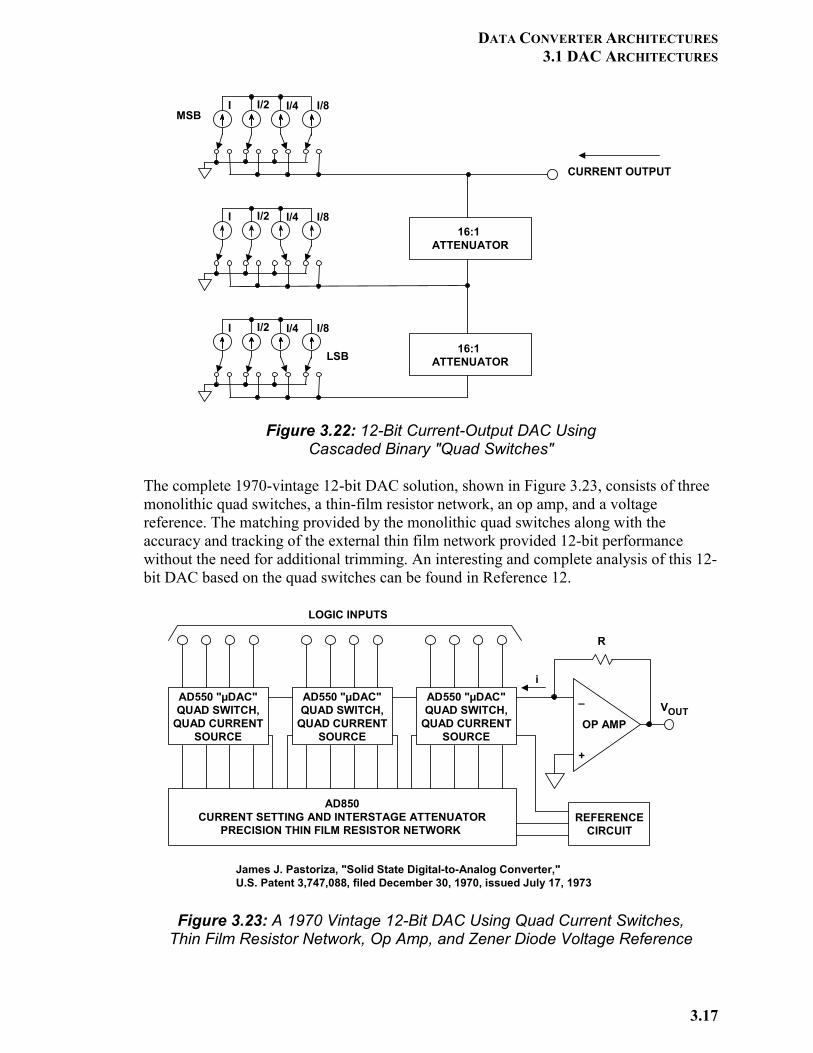
Figure 3.22 shows how three AD550 quad switches with 16:1 inter-stage attenuators are connected to form a 12-bit current-output DAC. Note that the maximum required resistor ratio of 16:1 is manageable. This monolithic "quad switch" (AD550 µDAC) along with a thin film resistor network (AD850), voltage reference, and an op amp formed the popular building blocks for 12-bit DACs in the early 1970s before the complete function was available in IC form several years later. The concept for the quad switch was patented by James J. Pastoriza (1970 filing, Reference 11).
VB
CURRENTOUTPUT
R 2R 4R 8R
I I/2 I/4 I/8
MSB
–V
EXTERNALTHIN FILMRESISTORNETWORK
VB
CURRENTOUTPUT
2R 2R 2R 2R
I I/2 I/4 I/8
MSB
–VR R R
2R
I/8
DATA CONVERTER ARCHITECTURES 3.1 DAC ARCHITECTURES
3.17
Figure 3.22: 12-Bit Current-Output DAC Using
Cascaded Binary "Quad Switches" The complete 1970-vintage 12-bit DAC solution, shown in Figure 3.23, consists of three monolithic quad switches, a thin-film resistor network, an op amp, and a voltage reference. The matching provided by the monolithic quad switches along with the accuracy and tracking of the external thin film network provided 12-bit performance without the need for additional trimming. An interesting and complete analysis of this 12-bit DAC based on the quad switches can be found in Reference 12.
Figure 3.23: A 1970 Vintage 12-Bit DAC Using Quad Current Switches,
Thin Film Resistor Network, Op Amp, and Zener Diode Voltage Reference
I/2 I/4 I/8IMSB
16:1 ATTENUATOR
I/2 I/4 I/8I
I/2 I/4 I/8I
16:1 ATTENUATORLSB
CURRENT OUTPUT
AD550 "µDAC"QUAD SWITCH,
QUAD CURRENTSOURCE
AD550 "µDAC"QUAD SWITCH,
QUAD CURRENTSOURCE
AD550 "µDAC"QUAD SWITCH,
QUAD CURRENTSOURCE
REFERENCECIRCUIT
+
–
AD850CURRENT SETTING AND INTERSTAGE ATTENUATOR
PRECISION THIN FILM RESISTOR NETWORK
R
i
VOUT
LOGIC INPUTS
James J. Pastoriza, "Solid State Digital-to-Analog Converter," U.S. Patent 3,747,088, filed December 30, 1970, issued July 17, 1973
OP AMP
ANALOG-DIGITAL CONVERSION
3.18
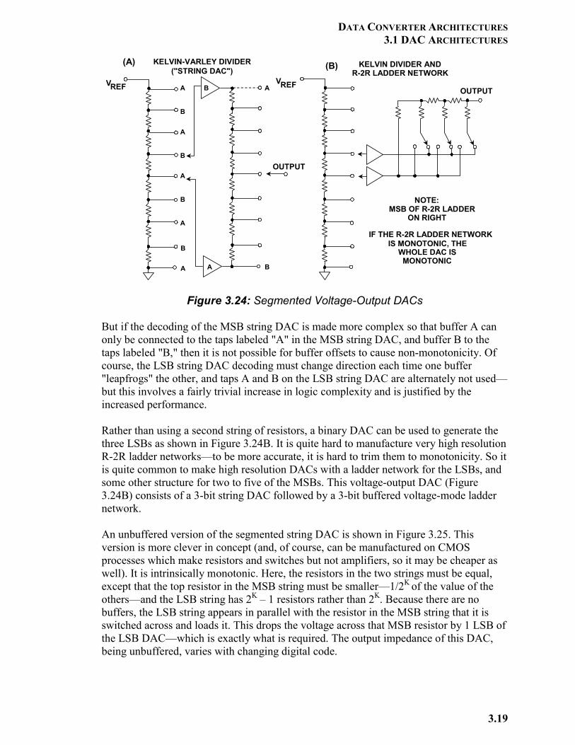
One of the problems in implementing a completely monolithic 12-bit DAC using the quad switch approach is that each 4-bit DAC requires emitter areas scaled 8:4:2:1. This requires a total of 15 unit emitter areas, and consumes a fairly large chip area. A few years after the introduction of the quad switch building block, Paul Brokaw of Analog Devices invented a technique in which only the first two current sources have an emitter scaling of 2:1. Subsequent current sources have the same unit emitter area but operate at different current densities—while still maintaining stable currents over temperature. Paul Brokaw's classic patent (filed in 1975) describes this technique in detail, and this particular patent is probably the most referenced and cited patent relating to data converters (Reference 13). Segmented DACs So far we have considered basic DAC architectures. When we are required to design a DAC with a specific performance, it may well be that no single architecture is ideal. In such cases, two or more DACs may be combined in a single higher resolution DAC to give the required performance. These DACs may be of the same type or of different types and need not each have the same resolution. In principle, one DAC handles the MSBs, another handles the LSBs, and their outputs are added in some way. The process is known as "segmentation," and these more complex structures are called "segmented DACs". There are many different types of segmented DACs and some, but by no means all, of them will be illustrated in the next few diagrams. Figure 3.24 shows two varieties of segmented voltage-output DAC. The architecture in Figure 3.24A is sometimes called a Kelvin-Varley Divider, or "string DAC." Since there are buffers between the first and second stages, the second string DAC does not load the first, and the resistors in this string do not need to have the same value as the resistors in the other one. All the resistors in each string, however, do need to be equal to each other or the DAC will not be linear. The examples shown have 3-bit first and second stages but for the sake of generality, let us refer to the first (MSB) stage resolution as M-bits and the second (LSB) as K-bits for a total of N = M + K bits. The MSB DAC has a string of 2M equal resistors, and a string of 2K equal resistors in the LSB DAC. Buffer amplifiers have offset, of course, and this can cause non-monotonicity in a buffered segmented string DAC. In the simpler configuration of a buffered Kelvin-Varley divider buffer (Figure 3.24A), buffer A is always "below" (at a lower potential than) buffer B, and the extra tap labeled "A" on the LSB string DAC is not necessary. The data decoding is just two priority encoders. In this configuration, however, buffer offset can cause non-monotonicity.
DATA CONVERTER ARCHITECTURES 3.1 DAC ARCHITECTURES
3.19
Figure 3.24: Segmented Voltage-Output DACs
But if the decoding of the MSB string DAC is made more complex so that buffer A can only be connected to the taps labeled "A" in the MSB string DAC, and buffer B to the taps labeled "B," then it is not possible for buffer offsets to cause non-monotonicity. Of course, the LSB string DAC decoding must change direction each time one buffer "leapfrogs" the other, and taps A and B on the LSB string DAC are alternately not used—but this involves a fairly trivial increase in logic complexity and is justified by the increased performance. Rather than using a second string of resistors, a binary DAC can be used to generate the three LSBs as shown in Figure 3.24B. It is quite hard to manufacture very high resolution R-2R ladder networks—to be more accurate, it is hard to trim them to monotonicity. So it is quite common to make high resolution DACs with a ladder network for the LSBs, and some other structure for two to five of the MSBs. This voltage-output DAC (Figure 3.24B) consists of a 3-bit string DAC followed by a 3-bit buffered voltage-mode ladder network. An unbuffered version of the segmented string DAC is shown in Figure 3.25. This version is more clever in concept (and, of course, can be manufactured on CMOS processes which make resistors and switches but not amplifiers, so it may be cheaper as well). It is intrinsically monotonic. Here, the resistors in the two strings must be equal, except that the top resistor in the MSB string must be smaller—1/2K of the value of the others—and the LSB string has 2K – 1 resistors rather than 2K. Because there are no buffers, the LSB string appears in parallel with the resistor in the MSB string that it is switched across and loads it. This drops the voltage across that MSB resistor by 1 LSB of the LSB DAC—which is exactly what is required. The output impedance of this DAC, being unbuffered, varies with changing digital code.
KELVIN-VARLEY DIVIDER("STRING DAC")
VREFVREF
OUTPUT
KELVIN DIVIDER ANDR-2R LADDER NETWORK
NOTE:MSB OF R-2R LADDER
ON RIGHT
IF THE R-2R LADDER NETWORKIS MONOTONIC, THE
WHOLE DAC ISMONOTONIC
OUTPUT
(A) (B)
A
B
A
B
A
B
A
B
A
A
B A
B
ANALOG-DIGITAL CONVERSION
3.20
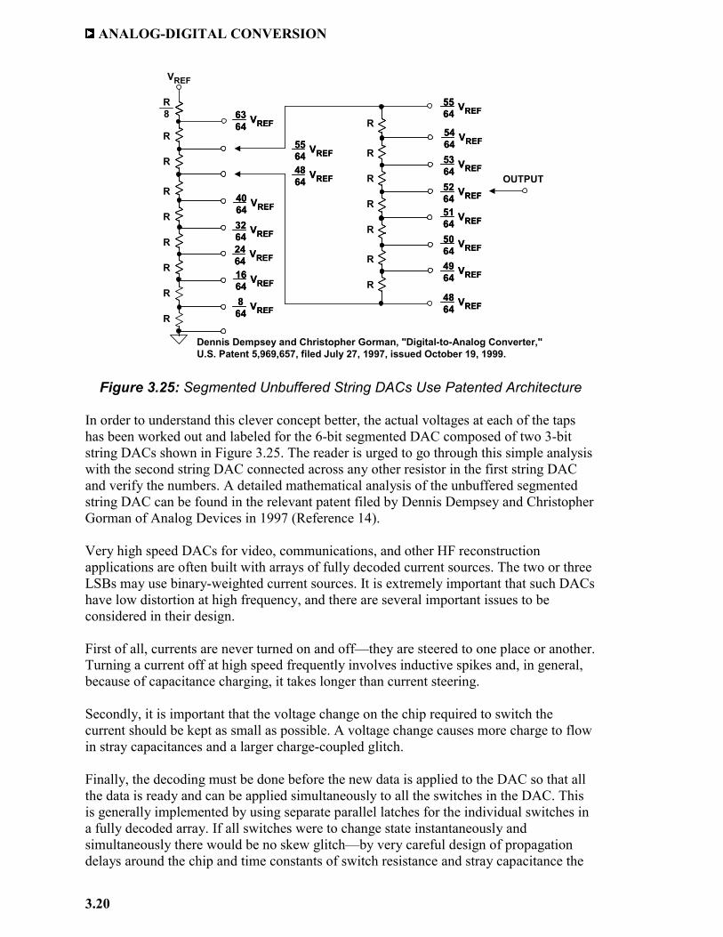
Figure 3.25: Segmented Unbuffered String DACs Use Patented Architecture
In order to understand this clever concept better, the actual voltages at each of the taps has been worked out and labeled for the 6-bit segmented DAC composed of two 3-bit string DACs shown in Figure 3.25. The reader is urged to go through this simple analysis with the second string DAC connected across any other resistor in the first string DAC and verify the numbers. A detailed mathematical analysis of the unbuffered segmented string DAC can be found in the relevant patent filed by Dennis Dempsey and Christopher Gorman of Analog Devices in 1997 (Reference 14). Very high speed DACs for video, communications, and other HF reconstruction applications are often built with arrays of fully decoded current sources. The two or three LSBs may use binary-weighted current sources. It is extremely important that such DACs have low distortion at high frequency, and there are several important issues to be considered in their design. First of all, currents are never turned on and off—they are steered to one place or another. Turning a current off at high speed frequently involves inductive spikes and, in general, because of capacitance charging, it takes longer than current steering. Secondly, it is important that the voltage change on the chip required to switch the current should be kept as small as possible. A voltage change causes more charge to flow in stray capacitances and a larger charge-coupled glitch. Finally, the decoding must be done before the new data is applied to the DAC so that all the data is ready and can be applied simultaneously to all the switches in the DAC. This is generally implemented by using separate parallel latches for the individual switches in a fully decoded array. If all switches were to change state instantaneously and simultaneously there would be no skew glitch—by very careful design of propagation delays around the chip and time constants of switch resistance and stray capacitance the
R
R
R
R
R
R
R
R
R8
VREF
6364
VREF6364
VREF
5564
VREF5564
VREF
5464
VREF5464
VREF
5364
VREF5364
VREF
5264
VREF5264
VREF
5164
VREF5164
VREF
5064
VREF5064
VREF
4964
VREF4964
VREF
4864
VREF4864
VREF
4064
VREF4064
VREF
3264
VREF3264
VREF
2464
VREF2464
VREF
1664
VREF1664
VREF
864
VREF864
VREF
OUTPUT
R
R
R
R
R
R
R
5564
VREF5564
VREF
4864
VREF4864
VREF
Dennis Dempsey and Christopher Gorman, "Digital-to-Analog Converter,"U.S. Patent 5,969,657, filed July 27, 1997, issued October 19, 1999.
DATA CONVERTER ARCHITECTURES 3.1 DAC ARCHITECTURES
3.21
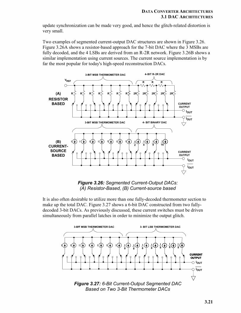
update synchronization can be made very good, and hence the glitch-related distortion is very small. Two examples of segmented current-output DAC structures are shown in Figure 3.26. Figure 3.26A shows a resistor-based approach for the 7-bit DAC where the 3 MSBs are fully decoded, and the 4 LSBs are derived from an R-2R network. Figure 3.26B shows a similar implementation using current sources. The current source implementation is by far the most popular for today's high-speed reconstruction DACs.
Figure 3.26: Segmented Current-Output DACs: (A) Resistor-Based, (B) Current-source based
It is also often desirable to utilize more than one fully-decoded thermometer section to make up the total DAC. Figure 3.27 shows a 6-bit DAC constructed from two fully-decoded 3-bit DACs. As previously discussed, these current switches must be driven simultaneously from parallel latches in order to minimize the output glitch.
Figure 3.27: 6-Bit Current-Output Segmented DAC Based on Two 3-Bit Thermometer DACs
R R R R R R R 2R2R 2R 2R 2R
R R RVREF
-3-BIT MSB THERMOMETER DAC 4-BIT R- 2R DAC
CURRENTOUTPUT
CURRENT
I I I I I I I I4
I2
I8
I16
-3-BIT MSB THERMOMETER DAC 4- BIT BINARY DAC
OUTPUT
(A)
(B)CURRENT-SOURCEBASED
IOUT
IOUT
IOUT
IOUT
RESISTORBASED
I I I I I I I I8
-3-BIT MSB THERMOMETER DAC 3- BIT LSB THERMOMETER DAC
CURRENTOUTPUT
CURRENTOUTPUT
CURRENTOUTPUT
I8
I8
I8
I8
I8
I8
IOUT
IOUT
ANALOG-DIGITAL CONVERSION
3.22
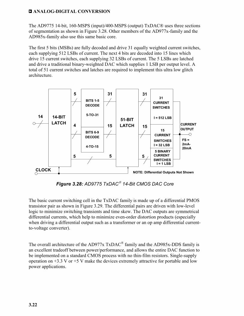
The AD9775 14-bit, 160-MSPS (input)/400-MSPS (output) TxDAC® uses three sections of segmentation as shown in Figure 3.28. Other members of the AD977x-family and the AD985x-family also use this same basic core. The first 5 bits (MSBs) are fully decoded and drive 31 equally weighted current switches, each supplying 512 LSBs of current. The next 4 bits are decoded into 15 lines which drive 15 current switches, each supplying 32 LSBs of current. The 5 LSBs are latched and drive a traditional binary-weighted DAC which supplies 1 LSB per output level. A total of 51 current switches and latches are required to implement this ultra low glitch architecture.
Figure 3.28: AD9775 TxDAC 14-Bit CMOS DAC Core
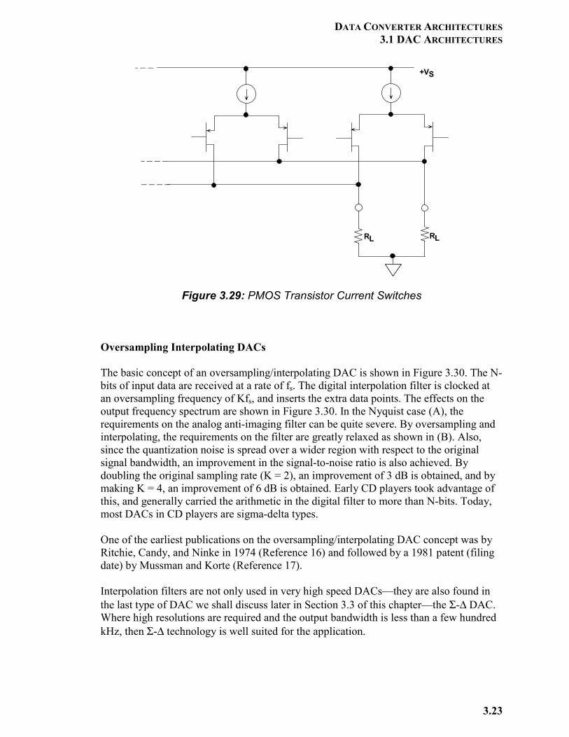
The basic current switching cell in the TxDAC family is made up of a differential PMOS transistor pair as shown in Figure 3.29. The differential pairs are driven with low-level logic to minimize switching transients and time skew. The DAC outputs are symmetrical differential currents, which help to minimize even-order distortion products (especially when driving a differential output such as a transformer or an op amp differential current-to-voltage converter). The overall architecture of the AD977x TxDAC® family and the AD985x-DDS family is an excellent tradeoff between power/performance, and allows the entire DAC function to be implemented on a standard CMOS process with no thin-film resistors. Single-supply operation on +3.3 V or +5 V make the devices extremely attractive for portable and low power applications.
CLOCK
14-BITLATCH
51-BITLATCH
31CURRENTSWITCHES
15CURRENT
5 BINARYCURRENTSWITCHES
BITS 1-5DECODE
5-TO-31
BITS 6-9DECODE
4-TO-15
5 5
15154
31 315
14
CURRENTOUTPUT
FS =2mA-20mA
SWITCHES
I = 512 LSB
I = 32 LSB
I = 1 LSB
5
NOTE: Differential Outputs Not Shown
DATA CONVERTER ARCHITECTURES 3.1 DAC ARCHITECTURES
3.23
Figure 3.29: PMOS Transistor Current Switches
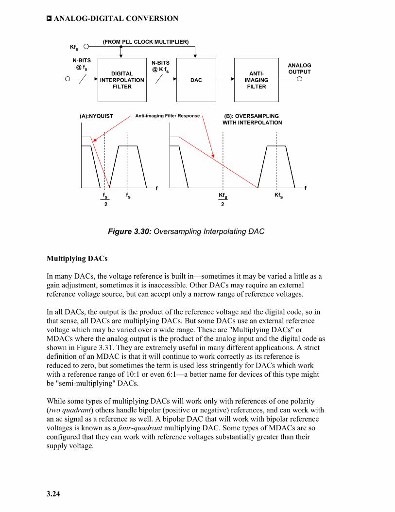
Oversampling Interpolating DACs The basic concept of an oversampling/interpolating DAC is shown in Figure 3.30. The N-bits of input data are received at a rate of fs. The digital interpolation filter is clocked at an oversampling frequency of Kfs, and inserts the extra data points. The effects on the output frequency spectrum are shown in Figure 3.30. In the Nyquist case (A), the requirements on the analog anti-imaging filter can be quite severe. By oversampling and interpolating, the requirements on the filter are greatly relaxed as shown in (B). Also, since the quantization noise is spread over a wider region with respect to the original signal bandwidth, an improvement in the signal-to-noise ratio is also achieved. By doubling the original sampling rate (K = 2), an improvement of 3 dB is obtained, and by making K = 4, an improvement of 6 dB is obtained. Early CD players took advantage of this, and generally carried the arithmetic in the digital filter to more than N-bits. Today, most DACs in CD players are sigma-delta types. One of the earliest publications on the oversampling/interpolating DAC concept was by Ritchie, Candy, and Ninke in 1974 (Reference 16) and followed by a 1981 patent (filing date) by Mussman and Korte (Reference 17). Interpolation filters are not only used in very high speed DACs—they are also found in the last type of DAC we shall discuss later in Section 3.3 of this chapter—the Σ-∆ DAC. Where high resolutions are required and the output bandwidth is less than a few hundred kHz, then Σ-∆ technology is well suited for the application.
RL
+VS
RL
ANALOG-DIGITAL CONVERSION
3.24
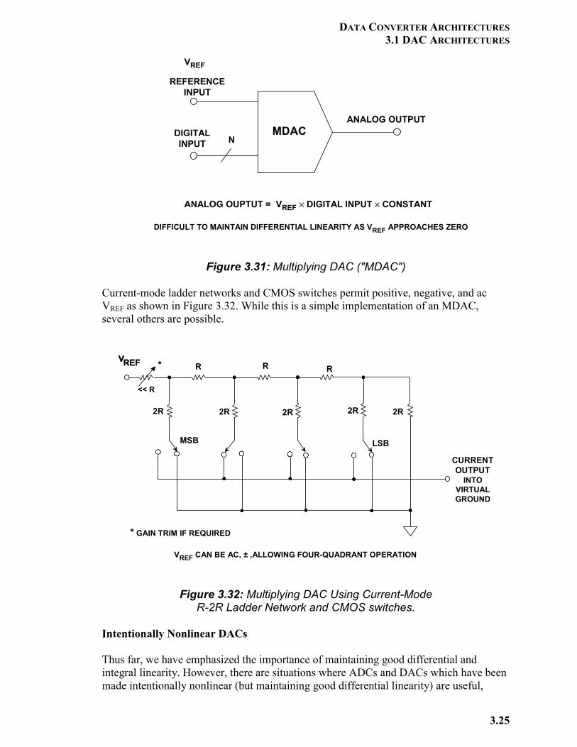
Figure 3.30: Oversampling Interpolating DAC Multiplying DACs In many DACs, the voltage reference is built in—sometimes it may be varied a little as a gain adjustment, sometimes it is inaccessible. Other DACs may require an external reference voltage source, but can accept only a narrow range of reference voltages. In all DACs, the output is the product of the reference voltage and the digital code, so in that sense, all DACs are multiplying DACs. But some DACs use an external reference voltage which may be varied over a wide range. These are "Multiplying DACs" or MDACs where the analog output is the product of the analog input and the digital code as shown in Figure 3.31. They are extremely useful in many different applications. A strict definition of an MDAC is that it will continue to work correctly as its reference is reduced to zero, but sometimes the term is used less stringently for DACs which work with a reference range of 10:1 or even 6:1—a better name for devices of this type might be "semi-multiplying" DACs. While some types of multiplying DACs will work only with references of one polarity (two quadrant) others handle bipolar (positive or negative) references, and can work with an ac signal as a reference as well. A bipolar DAC that will work with bipolar reference voltages is known as a four-quadrant multiplying DAC. Some types of MDACs are so configured that they can work with reference voltages substantially greater than their supply voltage.
DIGITALINTERPOLATION
FILTERDAC
ANTI-IMAGINGFILTER
N-BITS@ fs
N-BITS@ K fs
Kfs
ANALOGOUTPUT
fsfs2
KfsKfs2
f f
(A):NYQUIST (B): OVERSAMPLINGWITH INTERPOLATION
Anti-imaging Filter Response
(FROM PLL CLOCK MULTIPLIER)
DATA CONVERTER ARCHITECTURES 3.1 DAC ARCHITECTURES
3.25
Figure 3.31: Multiplying DAC ("MDAC") Current-mode ladder networks and CMOS switches permit positive, negative, and ac VREF as shown in Figure 3.32. While this is a simple implementation of an MDAC, several others are possible.
Figure 3.32: Multiplying DAC Using Current-Mode R-2R Ladder Network and CMOS switches.
Intentionally Nonlinear DACs Thus far, we have emphasized the importance of maintaining good differential and integral linearity. However, there are situations where ADCs and DACs which have been made intentionally nonlinear (but maintaining good differential linearity) are useful,
N
REFERENCEINPUT
DIGITALINPUT
ANALOG OUTPUT
ANALOG OUPTUT = VREF × DIGITAL INPUT × CONSTANT
VREF
MDAC
DIFFICULT TO MAINTAIN DIFFERENTIAL LINEARITY AS VREF APPROACHES ZERO
2R
RRR
2R2R2R2R
VREFVREF
MSB LSB
CURRENTOUTPUT
INTOVIRTUALGROUND
<< R
*
* GAIN TRIM IF REQUIRED
VREF CAN BE AC, ± ,ALLOWING FOUR-QUADRANT OPERATION
ANALOG-DIGITAL CONVERSION
3.26
especially when processing signals having a wide dynamic range. One of the earliest uses of nonlinear data converters was in the digitization of voiceband signals for pulse code modulation (PCM) systems. Major contributions were made at Bell Labs during the development of the T1 carrier system. The motive for the nonlinear ADCs and DACs was to reduce the total number of bits (and therefore the serial transmission rate) required to digitize voice channels. Straight linear encoding of a voice channel required 11- or 12-bits and a sampling rate of 8 kSPS per. In the 1960s Bell Labs determined that 7-bit nonlinear encoding was sufficient; and later in the 1970s they went to 8-bit nonlinear encoding for better performance (References 18-23). The nonlinear transfer function allocates more quantization levels out of the total range for small signals and fewer for large amplitude signals. In effect, this reduces the quantization noise associated with small signals (where it is most noticeable) and increases the quantization noise for larger signals (where it is less noticeable). The term companding is generally used to describe this form of encoding. The logarithmic transfer function chosen is referred to as the "Bell µ-255" standard, or simply "µ-law." A similar standard developed in Europe is referred to as "A-law." The Bell µ-law allows a dynamic range of about 4000:1 using 8 bits, whereas an 8-bit linear data converter provides a range of only 256:1. The first generation channel bank (D1) generated the logarithmic transfer function using temperature controlled resistor-diode networks for "compressors" ahead of a 7-bit linear ADC in the transmitter. Corresponding resistor-diode "expandors" having an inverse transfer function followed the 7-bit linear DAC in the receiver. The next generation D2 channel banks used nonlinear ADCs and DACs to accomplish the compression/expansion functions in a much more reliable and cost-effective manner, and eliminated the need for the temperature-controlled diode networks. In his 1953 classic paper, B. D. Smith proposed that the transfer function of a successive approximation ADC utilizing a nonlinear internal DAC in the feedback path would be the inverse transfer function of the DAC (Reference 8). The same basic DAC could therefore be used in the ADC and also for the reconstruction DAC. Later in the 1960s and early 1970s, nonlinear ADC and DAC technology using piecewise linear approximations of the desired transfer function allowed low cost, high volume implementations (References 18-23). These nonlinear 8-bit, 8-kSPS data converters became popular telecommunications building blocks. The nonlinear transfer function of the 8-bit DAC is first divided into 16 segments (chords) of different slopes—the slopes are determined by the desired nonlinear transfer function. The 4 MSBs determine the segment containing the desired data point, and the individual segment is further subdivided into 16 equal quantization levels by the 4 LSBs of the 8-bit word. This is shown in Figure 3.33 for a 6-bit DAC, where the first 3 bits identify one of the 8 possible chords, and each chord is further subdivided into 8 equal levels defined by the 3 LSBs. The 3 MSBs are generated using a nonlinear string DAC, and the 3 LSBs are generated using a 3-bit binary R-2R DAC.
DATA CONVERTER ARCHITECTURES 3.1 DAC ARCHITECTURES
3.27
Figure 3.33: Nonlinear 6-Bit Segmented DAC
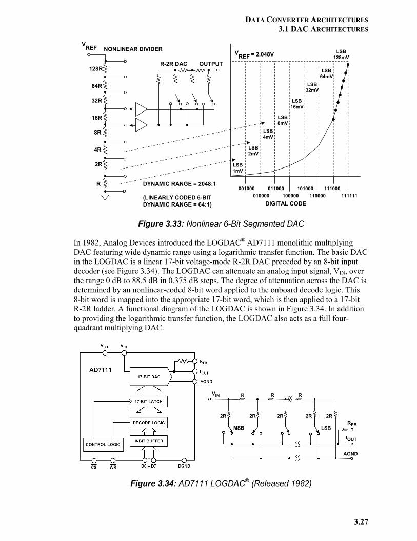
In 1982, Analog Devices introduced the LOGDAC® AD7111 monolithic multiplying DAC featuring wide dynamic range using a logarithmic transfer function. The basic DAC in the LOGDAC is a linear 17-bit voltage-mode R-2R DAC preceded by an 8-bit input decoder (see Figure 3.34). The LOGDAC can attenuate an analog input signal, VIN, over the range 0 dB to 88.5 dB in 0.375 dB steps. The degree of attenuation across the DAC is determined by an nonlinear-coded 8-bit word applied to the onboard decode logic. This 8-bit word is mapped into the appropriate 17-bit word, which is then applied to a 17-bit R-2R ladder. A functional diagram of the LOGDAC is shown in Figure 3.34. In addition to providing the logarithmic transfer function, the LOGDAC also acts as a full four-quadrant multiplying DAC.
Figure 3.34: AD7111 LOGDAC® (Released 1982)
VREF NONLINEAR DIVIDER
OUTPUT
VREF
R
2R
4R
8R
16R
32R
64R
128R
001000010000
011000100000
101000110000
111000111111
R-2R DAC
DIGITAL CODE
DYNAMIC RANGE = 2048:1
(LINEARLY CODED 6-BITDYNAMIC RANGE = 64:1)
= 2.048V
LSB1mV
LSB2mV
LSB4mV
LSB8mV
LSB16mV
LSB32mV
LSB64mV
LSB128mV
2R
RRR
2R2R2R2R
MSB LSB
VIN
IOUT
AGND
RFB
ANALOG-DIGITAL CONVERSION
3.28
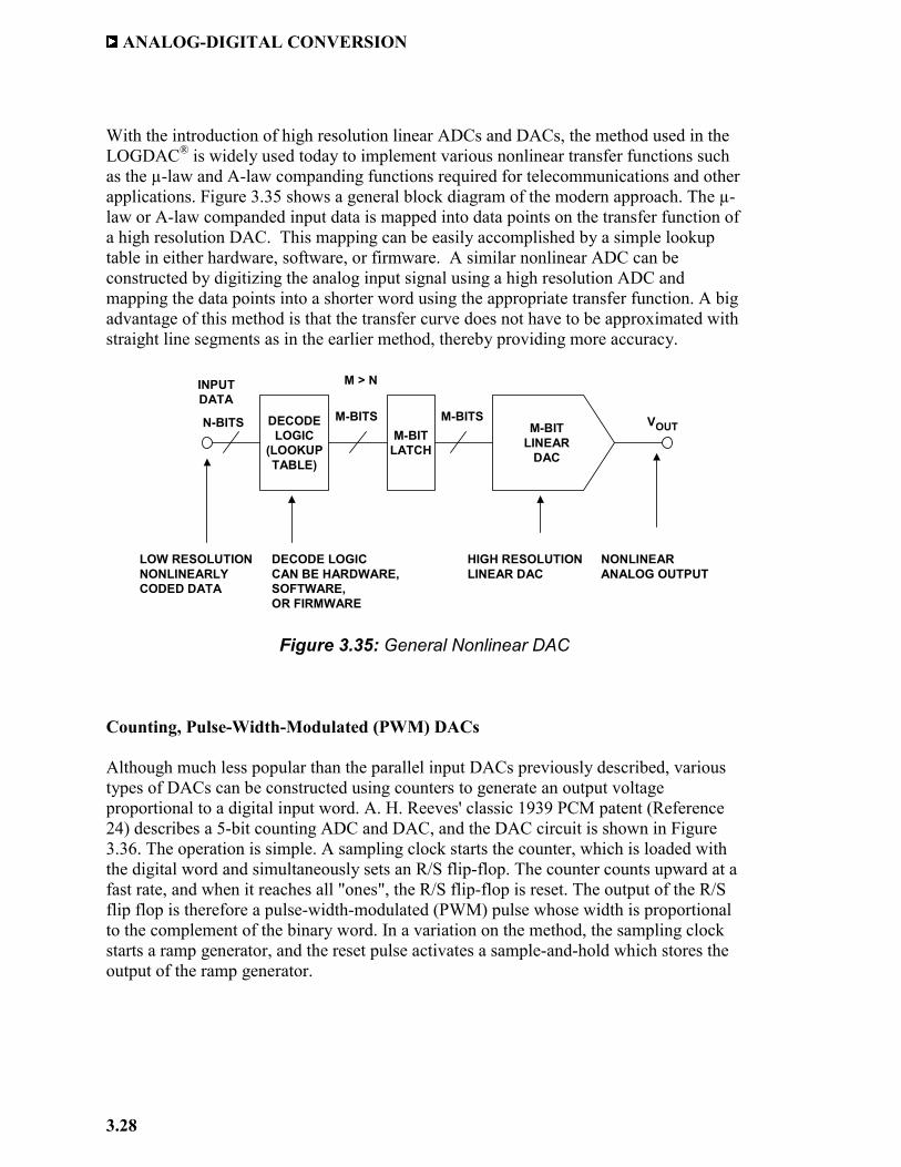
With the introduction of high resolution linear ADCs and DACs, the method used in the LOGDAC® is widely used today to implement various nonlinear transfer functions such as the µ-law and A-law companding functions required for telecommunications and other applications. Figure 3.35 shows a general block diagram of the modern approach. The µ-law or A-law companded input data is mapped into data points on the transfer function of a high resolution DAC. This mapping can be easily accomplished by a simple lookup table in either hardware, software, or firmware. A similar nonlinear ADC can be constructed by digitizing the analog input signal using a high resolution ADC and mapping the data points into a shorter word using the appropriate transfer function. A big advantage of this method is that the transfer curve does not have to be approximated with straight line segments as in the earlier method, thereby providing more accuracy.
Figure 3.35: General Nonlinear DAC
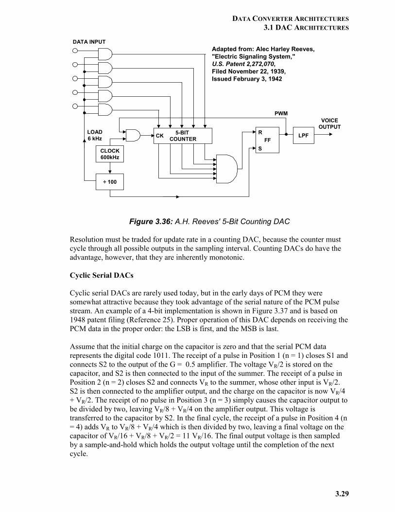
Counting, Pulse-Width-Modulated (PWM) DACs Although much less popular than the parallel input DACs previously described, various types of DACs can be constructed using counters to generate an output voltage proportional to a digital input word. A. H. Reeves' classic 1939 PCM patent (Reference 24) describes a 5-bit counting ADC and DAC, and the DAC circuit is shown in Figure 3.36. The operation is simple. A sampling clock starts the counter, which is loaded with the digital word and simultaneously sets an R/S flip-flop. The counter counts upward at a fast rate, and when it reaches all "ones", the R/S flip-flop is reset. The output of the R/S flip flop is therefore a pulse-width-modulated (PWM) pulse whose width is proportional to the complement of the binary word. In a variation on the method, the sampling clock starts a ramp generator, and the reset pulse activates a sample-and-hold which stores the output of the ramp generator.
M-BITLINEAR
DAC
DECODELOGIC
(LOOKUPTABLE)
M-BITLATCH
N-BITS
INPUTDATA
VOUTM-BITS M-BITS
M > N
DECODE LOGIC CAN BE HARDWARE, SOFTWARE, OR FIRMWARE
LOW RESOLUTIONNONLINEARLYCODED DATA
HIGH RESOLUTIONLINEAR DAC
NONLINEARANALOG OUTPUT
DATA CONVERTER ARCHITECTURES 3.1 DAC ARCHITECTURES
3.29
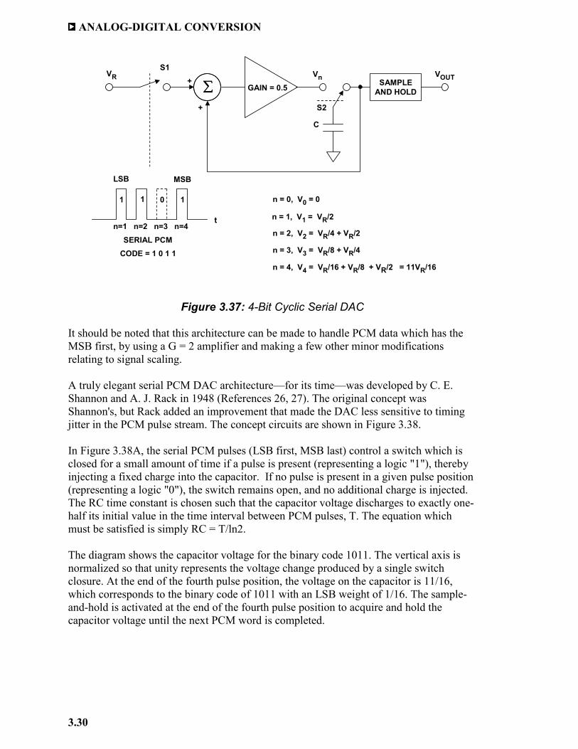
Figure 3.36: A.H. Reeves' 5-Bit Counting DAC Resolution must be traded for update rate in a counting DAC, because the counter must cycle through all possible outputs in the sampling interval. Counting DACs do have the advantage, however, that they are inherently monotonic. Cyclic Serial DACs Cyclic serial DACs are rarely used today, but in the early days of PCM they were somewhat attractive because they took advantage of the serial nature of the PCM pulse stream. An example of a 4-bit implementation is shown in Figure 3.37 and is based on 1948 patent filing (Reference 25). Proper operation of this DAC depends on receiving the PCM data in the proper order: the LSB is first, and the MSB is last. Assume that the initial charge on the capacitor is zero and that the serial PCM data represents the digital code 1011. The receipt of a pulse in Position 1 (n = 1) closes S1 and connects S2 to the output of the G = 0.5 amplifier. The voltage VR/2 is stored on the capacitor, and S2 is then connected to the input of the summer. The receipt of a pulse in Position 2 (n = 2) closes S2 and connects VR to the summer, whose other input is VR/2. S2 is then connected to the amplifier output, and the charge on the capacitor is now VR/4 + VR/2. The receipt of no pulse in Position 3 (n = 3) simply causes the capacitor output to be divided by two, leaving VR/8 + VR/4 on the amplifier output. This voltage is transferred to the capacitor by S2. In the final cycle, the receipt of a pulse in Position 4 (n = 4) adds VR to VR/8 + VR/4 which is then divided by two, leaving a final voltage on the capacitor of VR/16 + VR/8 + VR/2 = 11 VR/16. The final output voltage is then sampled by a sample-and-hold which holds the output voltage until the completion of the next cycle.
5-BIT COUNTER
CLOCK600kHz
÷ 100
FFR
S
LPF
PWM
LOAD6 kHz
DATA INPUT
VOICEOUTPUT
CK
Adapted from: Alec Harley Reeves, "Electric Signaling System," U.S. Patent 2,272,070, Filed November 22, 1939, Issued February 3, 1942
ANALOG-DIGITAL CONVERSION
3.30
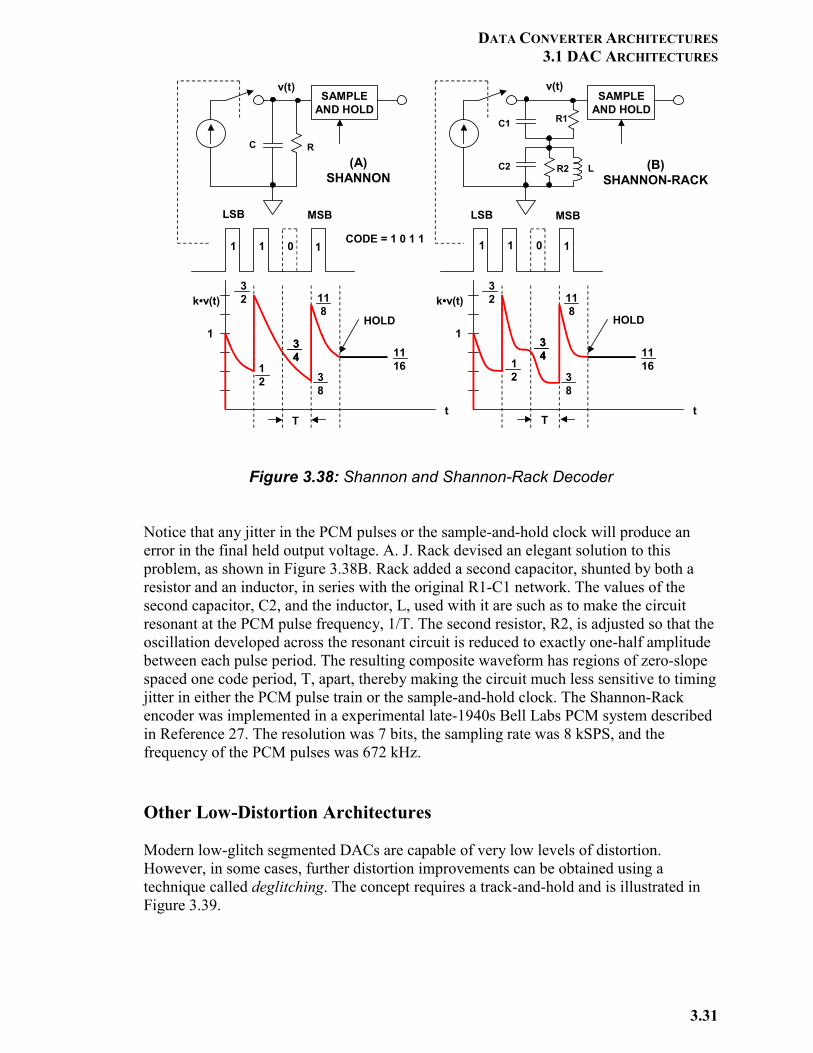
Figure 3.37: 4-Bit Cyclic Serial DAC It should be noted that this architecture can be made to handle PCM data which has the MSB first, by using a G = 2 amplifier and making a few other minor modifications relating to signal scaling. A truly elegant serial PCM DAC architecture—for its time—was developed by C. E. Shannon and A. J. Rack in 1948 (References 26, 27). The original concept was Shannon's, but Rack added an improvement that made the DAC less sensitive to timing jitter in the PCM pulse stream. The concept circuits are shown in Figure 3.38. In Figure 3.38A, the serial PCM pulses (LSB first, MSB last) control a switch which is closed for a small amount of time if a pulse is present (representing a logic "1"), thereby injecting a fixed charge into the capacitor. If no pulse is present in a given pulse position (representing a logic "0"), the switch remains open, and no additional charge is injected. The RC time constant is chosen such that the capacitor voltage discharges to exactly one-half its initial value in the time interval between PCM pulses, T. The equation which must be satisfied is simply RC = T/ln2. The diagram shows the capacitor voltage for the binary code 1011. The vertical axis is normalized so that unity represents the voltage change produced by a single switch closure. At the end of the fourth pulse position, the voltage on the capacitor is 11/16, which corresponds to the binary code of 1011 with an LSB weight of 1/16. The sample-and-hold is activated at the end of the fourth pulse position to acquire and hold the capacitor voltage until the next PCM word is completed.
SAMPLEAND HOLD
C
∑∑ GAIN = 0.5+
+
VR VOUT
LSB MSB
CODE = 1 0 1 1
Vn
n = 0, V0 = 0
t
SERIAL PCMn=1 n=2 n=3 n=4
n = 1, V1 = VR/2
n = 2, V2 = VR/4 + VR/2
n = 3, V3 = VR/8 + VR/4
n = 4, V4 = VR/16 + VR/8 + VR/2 = 11VR/16
S1
S2
1011
DATA CONVERTER ARCHITECTURES 3.1 DAC ARCHITECTURES
3.31
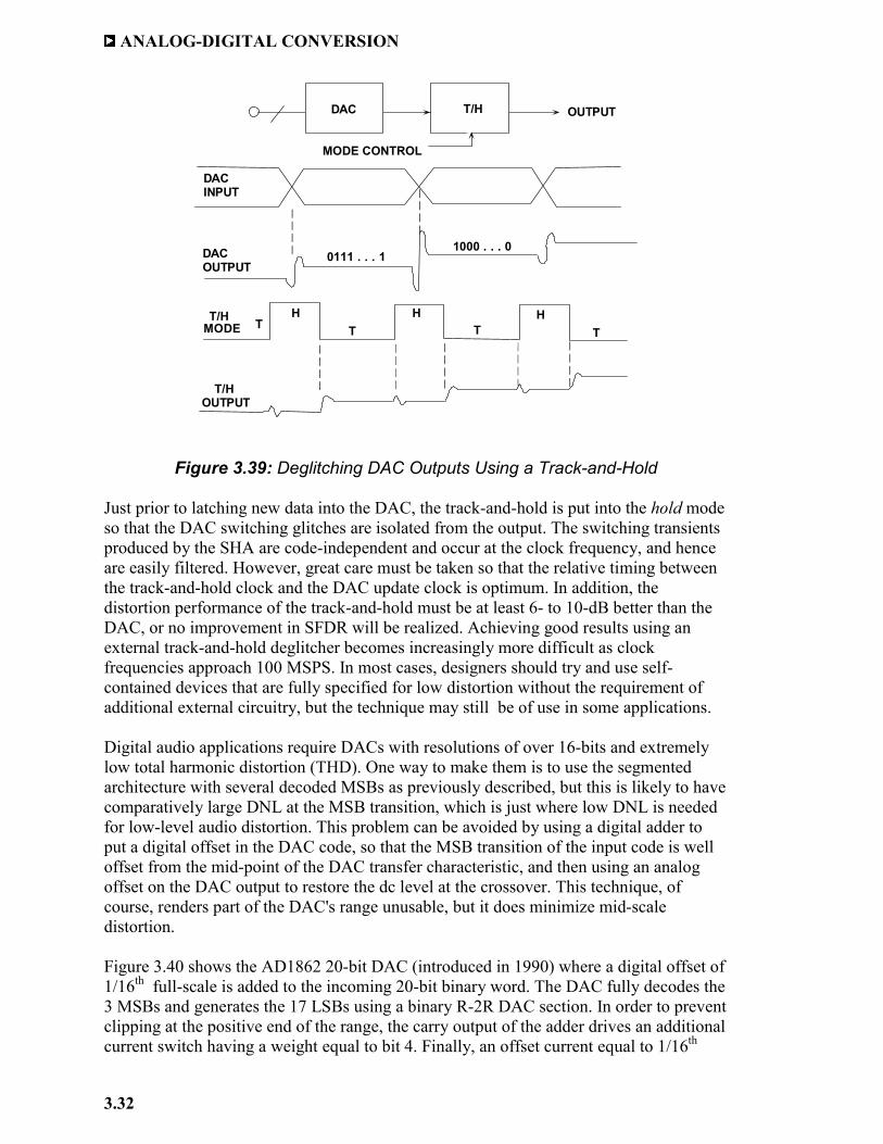
Figure 3.38: Shannon and Shannon-Rack Decoder Notice that any jitter in the PCM pulses or the sample-and-hold clock will produce an error in the final held output voltage. A. J. Rack devised an elegant solution to this problem, as shown in Figure 3.38B. Rack added a second capacitor, shunted by both a resistor and an inductor, in series with the original R1-C1 network. The values of the second capacitor, C2, and the inductor, L, used with it are such as to make the circuit resonant at the PCM pulse frequency, 1/T. The second resistor, R2, is adjusted so that the oscillation developed across the resonant circuit is reduced to exactly one-half amplitude between each pulse period. The resulting composite waveform has regions of zero-slope spaced one code period, T, apart, thereby making the circuit much less sensitive to timing jitter in either the PCM pulse train or the sample-and-hold clock. The Shannon-Rack encoder was implemented in a experimental late-1940s Bell Labs PCM system described in Reference 27. The resolution was 7 bits, the sampling rate was 8 kSPS, and the frequency of the PCM pulses was 672 kHz. Other Low-Distortion Architectures Modern low-glitch segmented DACs are capable of very low levels of distortion. However, in some cases, further distortion improvements can be obtained using a technique called deglitching. The concept requires a track-and-hold and is illustrated in Figure 3.39.
LSB MSB
1
32
38
118
1116
t
1
32
38
118
1116
t
SAMPLEAND HOLD
SAMPLEAND HOLD
R1C1
C2 R2 L
C R(A)
SHANNON(B)
SHANNON-RACK
LSB MSB
CODE = 1 0 1 1
12
12
1011 1011
3434
3434
v(t) v(t)
k•v(t)
HOLD HOLD
T T
k•v(t)
ANALOG-DIGITAL CONVERSION
3.32
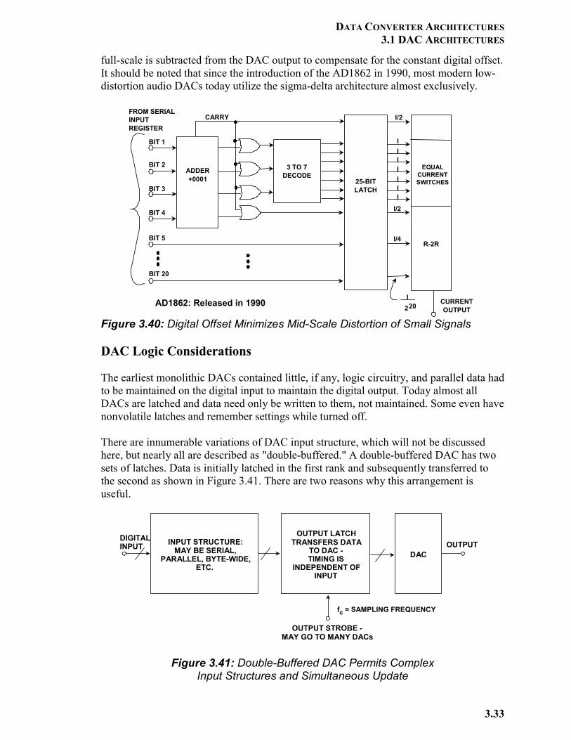
Figure 3.39: Deglitching DAC Outputs Using a Track-and-Hold Just prior to latching new data into the DAC, the track-and-hold is put into the hold mode so that the DAC switching glitches are isolated from the output. The switching transients produced by the SHA are code-independent and occur at the clock frequency, and hence are easily filtered. However, great care must be taken so that the relative timing between the track-and-hold clock and the DAC update clock is optimum. In addition, the distortion performance of the track-and-hold must be at least 6- to 10-dB better than the DAC, or no improvement in SFDR will be realized. Achieving good results using an external track-and-hold deglitcher becomes increasingly more difficult as clock frequencies approach 100 MSPS. In most cases, designers should try and use self-contained devices that are fully specified for low distortion without the requirement of additional external circuitry, but the technique may still be of use in some applications. Digital audio applications require DACs with resolutions of over 16-bits and extremely low total harmonic distortion (THD). One way to make them is to use the segmented architecture with several decoded MSBs as previously described, but this is likely to have comparatively large DNL at the MSB transition, which is just where low DNL is needed for low-level audio distortion. This problem can be avoided by using a digital adder to put a digital offset in the DAC code, so that the MSB transition of the input code is well offset from the mid-point of the DAC transfer characteristic, and then using an analog offset on the DAC output to restore the dc level at the crossover. This technique, of course, renders part of the DAC's range unusable, but it does minimize mid-scale distortion. Figure 3.40 shows the AD1862 20-bit DAC (introduced in 1990) where a digital offset of 1/16th full-scale is added to the incoming 20-bit binary word. The DAC fully decodes the 3 MSBs and generates the 17 LSBs using a binary R-2R DAC section. In order to prevent clipping at the positive end of the range, the carry output of the adder drives an additional current switch having a weight equal to bit 4. Finally, an offset current equal to 1/16th
DACINPUT
OUTPUT
DACOUTPUT
MODE
OUTPUT
T TH
TH
T
DAC
MODE CONTROL
0111 . . . 11000 . . . 0
H
T/H
T/H
T/H
DATA CONVERTER ARCHITECTURES 3.1 DAC ARCHITECTURES
3.33
full-scale is subtracted from the DAC output to compensate for the constant digital offset. It should be noted that since the introduction of the AD1862 in 1990, most modern low-distortion audio DACs today utilize the sigma-delta architecture almost exclusively.
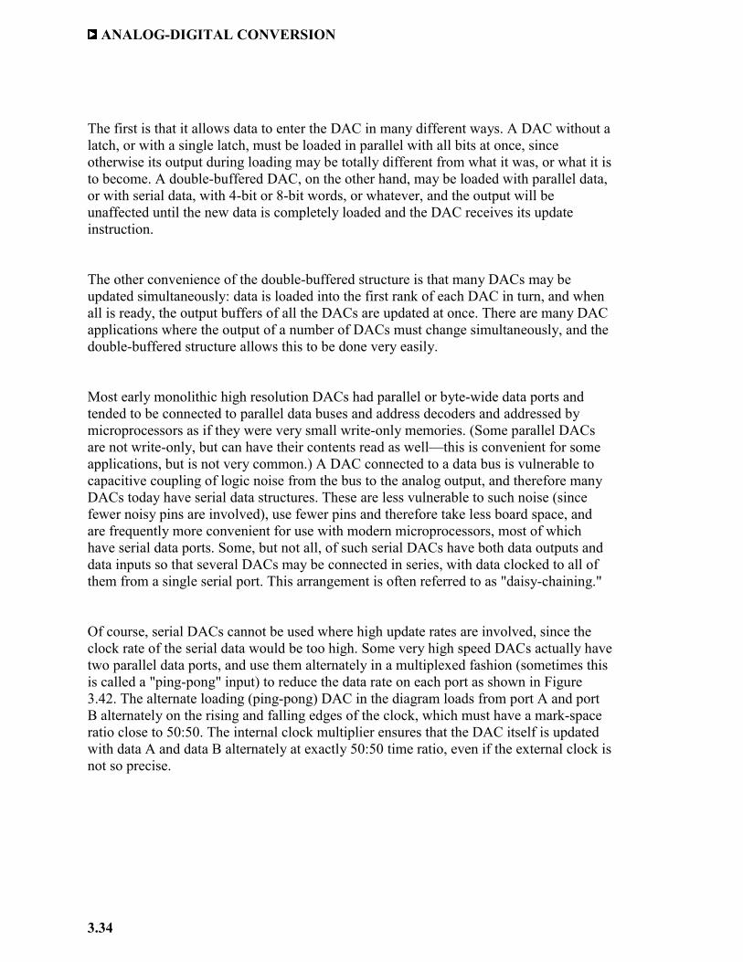
Figure 3.40: Digital Offset Minimizes Mid-Scale Distortion of Small Signals DAC Logic Considerations The earliest monolithic DACs contained little, if any, logic circuitry, and parallel data had to be maintained on the digital input to maintain the digital output. Today almost all DACs are latched and data need only be written to them, not maintained. Some even have nonvolatile latches and remember settings while turned off. There are innumerable variations of DAC input structure, which will not be discussed here, but nearly all are described as "double-buffered." A double-buffered DAC has two sets of latches. Data is initially latched in the first rank and subsequently transferred to the second as shown in Figure 3.41. There are two reasons why this arrangement is useful.
Figure 3.41: Double-Buffered DAC Permits Complex
Input Structures and Simultaneous Update
BIT 1
BIT 2
BIT 3
BIT 4
BIT 5
ADDER+0001
CARRY
CURRENTOUTPUT
25-BITLATCH
EQUALCURRENTSWITCHES
BIT 20
R-2R
3 TO 7DECODE
FROM SERIALINPUTREGISTER
IIIIIII
I/2
I/2
I/4
I220AD1862: Released in 1990
OUTPUTDIGITALINPUT INPUT STRUCTURE:
MAY BE SERIAL,PARALLEL, BYTE-WIDE,
ETC.
OUTPUT LATCHTRANSFERS DATA
TO DAC -TIMING IS
INDEPENDENT OFINPUT
DAC
OUTPUT STROBE -MAY GO TO MANY DACs
fc = SAMPLING FREQUENCY
ANALOG-DIGITAL CONVERSION
3.34
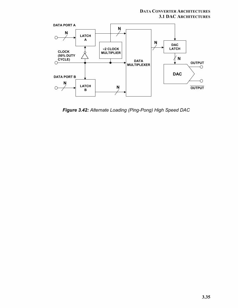
The first is that it allows data to enter the DAC in many different ways. A DAC without a latch, or with a single latch, must be loaded in parallel with all bits at once, since otherwise its output during loading may be totally different from what it was, or what it is to become. A double-buffered DAC, on the other hand, may be loaded with parallel data, or with serial data, with 4-bit or 8-bit words, or whatever, and the output will be unaffected until the new data is completely loaded and the DAC receives its update instruction. The other convenience of the double-buffered structure is that many DACs may be updated simultaneously: data is loaded into the first rank of each DAC in turn, and when all is ready, the output buffers of all the DACs are updated at once. There are many DAC applications where the output of a number of DACs must change simultaneously, and the double-buffered structure allows this to be done very easily. Most early monolithic high resolution DACs had parallel or byte-wide data ports and tended to be connected to parallel data buses and address decoders and addressed by microprocessors as if they were very small write-only memories. (Some parallel DACs are not write-only, but can have their contents read as well—this is convenient for some applications, but is not very common.) A DAC connected to a data bus is vulnerable to capacitive coupling of logic noise from the bus to the analog output, and therefore many DACs today have serial data structures. These are less vulnerable to such noise (since fewer noisy pins are involved), use fewer pins and therefore take less board space, and are frequently more convenient for use with modern microprocessors, most of which have serial data ports. Some, but not all, of such serial DACs have both data outputs and data inputs so that several DACs may be connected in series, with data clocked to all of them from a single serial port. This arrangement is often referred to as "daisy-chaining." Of course, serial DACs cannot be used where high update rates are involved, since the clock rate of the serial data would be too high. Some very high speed DACs actually have two parallel data ports, and use them alternately in a multiplexed fashion (sometimes this is called a "ping-pong" input) to reduce the data rate on each port as shown in Figure 3.42. The alternate loading (ping-pong) DAC in the diagram loads from port A and port B alternately on the rising and falling edges of the clock, which must have a mark-space ratio close to 50:50. The internal clock multiplier ensures that the DAC itself is updated with data A and data B alternately at exactly 50:50 time ratio, even if the external clock is not so precise.
DATA CONVERTER ARCHITECTURES 3.1 DAC ARCHITECTURES
3.35
Figure 3.42: Alternate Loading (Ping-Pong) High Speed DAC
DATAMULTIPLEXER
DACLATCH
DAC
N
NLATCH
A
LATCHB
×2 CLOCKMULTIPLIER
N
N
N
N
DATA PORT A
DATA PORT B
CLOCK(50% DUTYCYCLE)
OUTPUT
OUTPUT
ANALOG-DIGITAL CONVERSION
3.36
REFERENCES: 3.1 DAC ARCHITECTURES 1. Peter I. Wold, "Signal-Receiving System," U.S. Patent 1,514,753, filed November 19, 1920, issued
November 11, 1924. (thermometer DAC using relays and vacuum tubes). 2. Clarence A. Sprague, "Selective System," U.S. Patent 1,593,993, filed November 10, 1921, issued
July 27, 1926. (thermometer DAC using relays and vacuum tubes). 3. Leland K. Swart, "Gas-Filled Tube and Circuit Therefor," U.S. Patent 2,032,514, filed June 1, 1935,
issued March 3, 1936. (a thermometer DAC based on vacuum tube switches). 4. Robert Adams, Khiem Nguyen, and Karl Sweetland, "A 113 dB SNR Oversampling DAC with
Segmented Noise-Shaped Scrambling, " ISSCC Digest of Technical Papers, vol. 41, 1998, pp. 62, 63, 413. (describes a segmented audio DAC with data scrambling).
5. Robert W. Adams and Tom W. Kwan, "Data-directed Scrambler for Multi-bit Noise-shaping D/A
Converters," U.S. Patent 5,404,142, filed August 5, 1993, issued April 4, 1995. (describes a segmented audio DAC with data scrambling).
6. Paul M. Rainey, "Facimile Telegraph System," U.S. Patent 1,608,527, filed July 20, 1921, issued
November 30, 1926. (the first PCM patent. Also shows a relay-based 5-bit electro-mechanical flash converter and a binary DAC using relays and multiple resistors).
7. John C. Schelleng, "Code Modulation Communication System," U.S. Patent 2,453,461, Filed June 19,
1946, Issued November 9, 1948. (vacuum tube binary DAC using binary weighted voltages summed into load resistor with equal resistor weights).
8. B. D. Smith, "Coding by Feedback Methods," Proceedings of the I. R. E., Vol. 41, August 1953, pp.
1053-1058. (Smith uses an internal binary weighted DAC and also points out that a non-linear transfer function can be achieved by using a DAC with non-uniform bit weights, a technique which is widely used in today's voiceband ADCs with built-in companding. He was also one of the first to propose using an R/2R ladder network within the DAC core).
9. Bruce K. Smith, "Digital Attenuator," U.S. Patent 1,976,527, filed July 17, 1958, issued March 21,
1961. (describes a transistorized voltage output DAC similar to B. D. Smith above). 10. Bernard M. Gordon and Robert P. Talambiras, "Signal Conversion Apparatus," U.S. Patent 3,108,266,
filed July 22, 1955, issued October 22, 1963. (classic patent describing Gordon's 11-bit, 50kSPS vacuum tube successive approximation ADC done at Epsco. The internal DAC represents the first known use of equal currents switched into an R/2R ladder network.)
11. James J. Pastoriza, "Solid State Digital-to-Analog Converter," U.S. Patent 3,747,088, filed December
30, 1970, issued July 17, 1973. (the first patent on the quad switch approach to building high resolution DACs).
12. Eugene R. Hnatek, A User's Handbook of D/A and A/D Converters, John Wiley, New York, 1976,
ISBN 0-471-40109-9, pp. 282-295. (contains an excellent description of the Analog Devices' AD550 monolithic µDAC quad current switch, and AD850 thin film network—building blocks for 12-bit DACs introduced in 1970 ).
13. Adrian Paul Brokaw, "Digital-to-Analog Converter with Current Source Transistors Operated
Accurately at Different Current Densities," U.S. Patent 3,940,760, filed March 21, 1975, issued February 24, 1976. (the most referenced data converter patent ever issued).
DATA CONVERTER ARCHITECTURES 3.1 DAC ARCHITECTURES
3.37
14. Dennis Dempsey and Christopher Gorman, "Digital-to-Analog Converter," U.S. Patent 5,969,657, filed July 27, 1997, issued October 19, 1999. (describes an elegant solution for segmented unbuffered string DACs).
15. John A. Schoeff, "An Inherently Monotonic 12 Bit DAC," IEEE Journal of Solid State Circuits,
Vol. SC-14, No. 6, December 1979, pp. 904-911. (describes one of the first monolithic DACs to use segmentation).
16. G. R. Ritchie, J. C. Candy, and W. H. Ninke, "Interpolative Digital-to-Analog Converters," IEEE
Transactions on Communications, Vol. COM-22, November 1974, pp. 1797-1806. (one of the earliest papers written on oversampling interpolative DACs).
17. H. G. Musmann and W. W. Korte, "Generalized Interpolative Method for Digital/Analog Conversion
of PCM Signals," U.S. Patent 4,467,316, filed June 3, 1981, issued August 21, 1984. (a description of interpolating DACs).
18. B. Smith, "Instantaneous Companding of Quantized Signals, Bell System Technical Journal, Vol. 36,
May 1957, pp. 653-709. (one of the first papers written about using nonlinear coding techniques for speech signals in PCM).
19. H. Kaneko and T. Sekimoto, "Logarithmic PCM Encoding Without Diode Compandor," IEEE
Transactions on Communications Systems, Vol. 11, No. 3, September 1963, pp. 296-307. (describes several methods for nonlinear encoding speech directly without the need for diode compandors).
20. C. L. Dammann, "An Approach to Logarithmic Coders and Decoders," NEREM Record, Boston MA,
November 2-4, 1966, pp. 196-197. (more discussions on nonlinear coders and decoders for PCM). 21. H. Kaneko, "A Unified Formulation of Segment Companding Laws and Synthesis of Codecs and
Digital Compandors," Bell System Technical Journal, Vol. 49, September 1970, pp. 1555-1558. (discusses the piecewise linear approximation to the logarithmic transfer companding function).
22. M. R. Aaron and H. Kaneko, "Synthesis of Digital Attenuators for Segment Companded PCM Codes,"
Transactions on Communications Technology, COM-19, December 1971, pp. 1076-1087. (more on nonlinear coding).
23. C. L. Dammann, L. D. McDaniel, and C. L. Maddox, "D2 Channel Bank: Multiplexing and Coding,"
Bell System Technical Journal, Vol. 51, October 1972, pp. 1675-1699. (still more on nonlinear coding).
24. A.H. Reeves, "Electric Signaling System," U.S. Patent 2,272,070, filed November 22, 1939, issued
February 3, 1942. (Reeves' classic PCM patent which describes a 5-bit PWM counting ADC and DAC).
25. R. L. Carbrey, "Decoder for Pulse Code Modulation," U.S. Patent 2,579,302, filed January 17, 1948,
issued December 18, 1951. (describes cyclic or sequential attenuation DAC). 26. R. L. Carbrey, "Decoding in PCM,", Bell Labs Record, November 1948, pp. 451-456. (describes the
Shannon-Rack PCM DAC). 27. L.A. Meacham and E. Peterson, "An Experimental Multichannel Pulse Code Modulation System of
Toll Quality," Bell System Technical Journal, Vol. 27, No. 1, January 1948, pp. 1-43. (further details of the Shannon-Rack decoder as part of the experimental PCM system).

ANALOG-DIGITAL CONVERSION
3.38
NOTES:
DATA CONVERTER ARCHITECTURES 3.2 ADC ARCHITECTURES
3.39
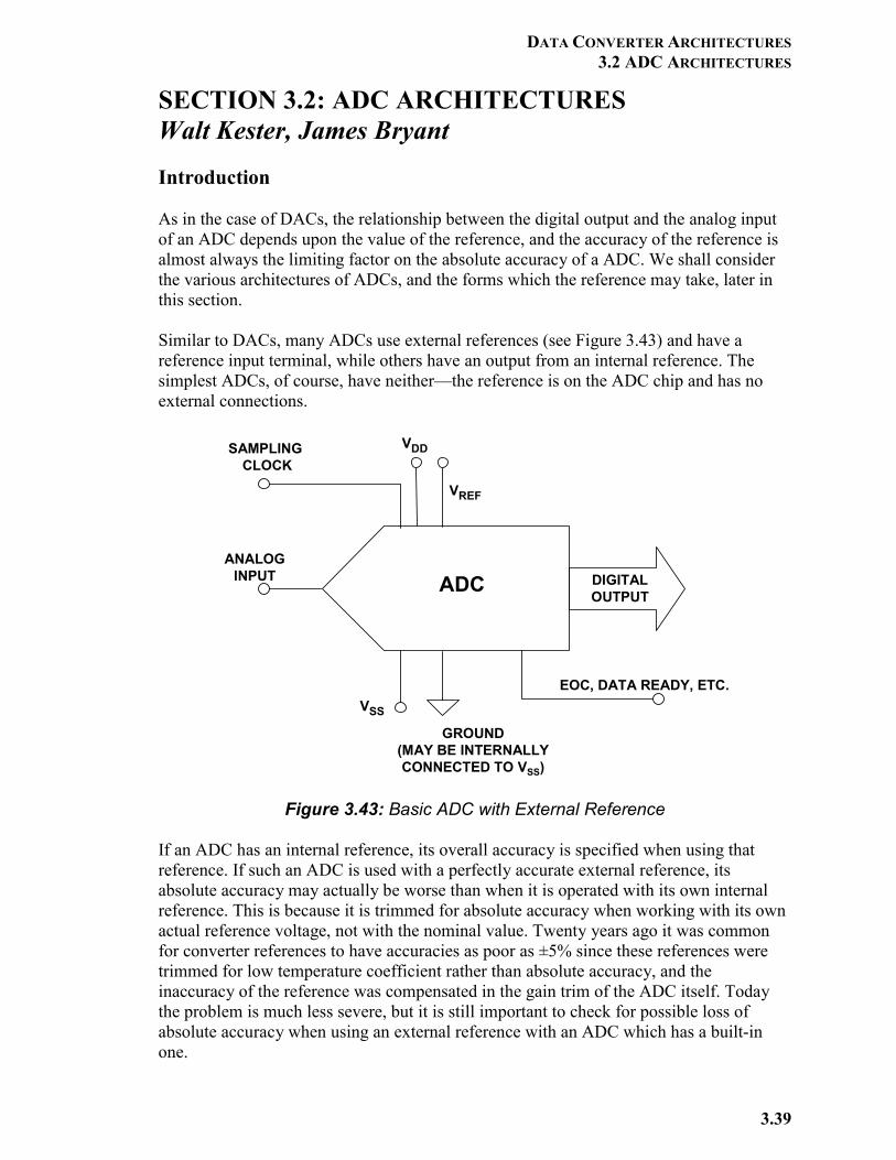
SECTION 3.2: ADC ARCHITECTURES Walt Kester, James Bryant Introduction As in the case of DACs, the relationship between the digital output and the analog input of an ADC depends upon the value of the reference, and the accuracy of the reference is almost always the limiting factor on the absolute accuracy of a ADC. We shall consider the various architectures of ADCs, and the forms which the reference may take, later in this section. Similar to DACs, many ADCs use external references (see Figure 3.43) and have a reference input terminal, while others have an output from an internal reference. The simplest ADCs, of course, have neither—the reference is on the ADC chip and has no external connections.
Figure 3.43: Basic ADC with External Reference
If an ADC has an internal reference, its overall accuracy is specified when using that reference. If such an ADC is used with a perfectly accurate external reference, its absolute accuracy may actually be worse than when it is operated with its own internal reference. This is because it is trimmed for absolute accuracy when working with its own actual reference voltage, not with the nominal value. Twenty years ago it was common for converter references to have accuracies as poor as ±5% since these references were trimmed for low temperature coefficient rather than absolute accuracy, and the inaccuracy of the reference was compensated in the gain trim of the ADC itself. Today the problem is much less severe, but it is still important to check for possible loss of absolute accuracy when using an external reference with an ADC which has a built-in one.
VDD
VSS
GROUND(MAY BE INTERNALLY CONNECTED TO VSS)
ADCANALOG
INPUT
VREF
DIGITALOUTPUT
SAMPLING CLOCK
EOC, DATA READY, ETC.
ANALOG-DIGITAL CONVERSION
3.40
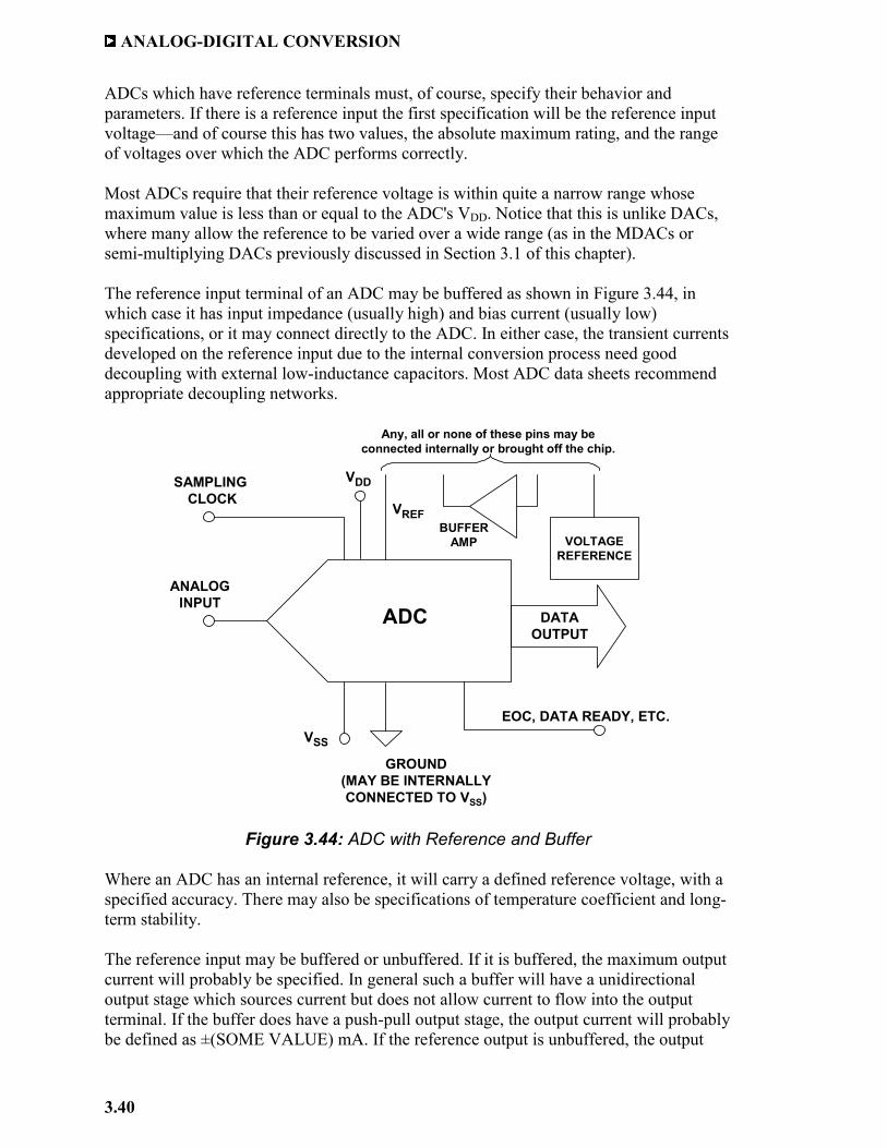
ADCs which have reference terminals must, of course, specify their behavior and parameters. If there is a reference input the first specification will be the reference input voltage—and of course this has two values, the absolute maximum rating, and the range of voltages over which the ADC performs correctly. Most ADCs require that their reference voltage is within quite a narrow range whose maximum value is less than or equal to the ADC's VDD. Notice that this is unlike DACs, where many allow the reference to be varied over a wide range (as in the MDACs or semi-multiplying DACs previously discussed in Section 3.1 of this chapter). The reference input terminal of an ADC may be buffered as shown in Figure 3.44, in which case it has input impedance (usually high) and bias current (usually low) specifications, or it may connect directly to the ADC. In either case, the transient currents developed on the reference input due to the internal conversion process need good decoupling with external low-inductance capacitors. Most ADC data sheets recommend appropriate decoupling networks.
Figure 3.44: ADC with Reference and Buffer
Where an ADC has an internal reference, it will carry a defined reference voltage, with a specified accuracy. There may also be specifications of temperature coefficient and long-term stability. The reference input may be buffered or unbuffered. If it is buffered, the maximum output current will probably be specified. In general such a buffer will have a unidirectional output stage which sources current but does not allow current to flow into the output terminal. If the buffer does have a push-pull output stage, the output current will probably be defined as ±(SOME VALUE) mA. If the reference output is unbuffered, the output
VDD
VSS
GROUND(MAY BE INTERNALLY CONNECTED TO VSS)
ADCANALOG
INPUT
VREF
VOLTAGEREFERENCE
Any, all or none of these pins may beconnected internally or brought off the chip.
BUFFERAMP
DATAOUTPUT
SAMPLING CLOCK
EOC, DATA READY, ETC.
DATA CONVERTER ARCHITECTURES 3.2 ADC ARCHITECTURES
3.41
impedance may be specified, or the data sheet may simply advise the use of a high input impedance external buffer. The sampling clock input (sometimes called convert-start or encode command) is a critical function in an ADC and a source of some confusion. Many of the early integrated circuit ADCs (such as the industry-standard AD574) did not have a built-in sample-and-hold function, and were known simply as encoders. These converters required an external clock to begin the conversion process. In the case of the AD574, the application of the external clock initiated an internal high-speed clock oscillator which in turn controlled the actual conversion process. Most modern ADCs have the sample-and-hold function on-chip and require an external sampling clock to initiate the conversion. In some ADCs, only a single sampling clock is required—in others, both a high frequency clock as well as a lower speed sampling clock are required. Regardless of the ADC, it is extremely important to read the data sheet and determine exactly what the external clock requirements are because they can vary widely from one ADC to another, since there is no standard. At some point after the assertion of the sampling clock, the output data is valid. This data may be in parallel or serial format depending upon the ADC. Early successive approximation ADCs such as the AD574 simply provided a STATUS output (STS) which went high during the conversion, and returned to the low state when the output data was valid. In other ADCs, this line is variously called busy, end-of-conversion (EOC), data ready, etc. Regardless of the ADC, there must be some method of knowing when the output data is valid—and again, the data sheet is where this information can always be found. There are one or two other practical points which are worth remembering about the logic of ADCs. On power-up, many ADCs do not have logic reset circuitry and may enter an anomalous logical state. One or two conversions may be necessary to restore their logic to proper operation so: (a) the first and second conversions after power-up should never be trusted, and (b) control outputs (EOC, data ready, etc.) may behave in unexpected ways at this time (and not necessarily in the same way at each power-up), and (c) care should be taken to ensure that such anomalous behavior cannot cause system latch-up. For example, EOC (end-of-conversion) should not be used to initiate conversion if there is any possibility that EOC will not occur until the first conversion has taken place, as otherwise initiation will never occur. Some low-power ADCs now have power-saving modes of operation variously called standby, power-down, sleep, etc. When an ADC comes out of one of these low-power modes, there is a certain recovery time required before the ADC can operate at its full specified performance. The data sheet should therefore be carefully studied when using these modes of operation, and there may be several different levels of power-down. Another detail which can cause trouble is the difference between EOC and DRDY (data ready). EOC indicates that conversion has finished, DRDY that data is available at the output. In some ADCs, EOC functions as DRDY—in others, data is not valid until several tens of nanoseconds after the EOC has become valid, and if EOC is used as a data strobe, the results will be unreliable.
ANALOG-DIGITAL CONVERSION
3.42
As a final example, some ADCs use CS (Chip Select) edges to reset internal logic, and it may not be possible to perform another conversion without asserting or reasserting CS (or it may not be possible to read the same data twice, or both). For more detail, it is important to read the whole data sheet before using an ADC since there are innumerable small logic variations from type to type. Unfortunately, many data sheets are not as clear as one might wish, so it is also important to understand the general principles of ADCs in order to interpret data sheets correctly. That is one of the purposes of this section. We are now ready to discuss the various architectures for ADCs. Because it is a fundamental building block used in all ADCs, the comparator (a 1-bit ADC) is treated first. It is logical to follow this with the flash converter architecture because it is somewhat analogous to the fully-decoded (thermometer) DAC architecture previously discussed. The successive approximation ADC architecture is treated next followed by subranging and pipelined architectures. The folding (Gray-code) architecture completes the primary architectures used in so-called high-speed ADCs. The last part of this sections discusses the various counting and integrating architectures which are generally more suited to high resolution lower speed ADCs. Sigma-Delta (Σ-∆) ADCs and DACs are treated in a separate section which concludes this chapter. The Comparator: A 1-Bit ADC As a changeover switch is a 1-bit DAC, so a comparator is a 1-bit ADC (see Figure 3.45). If the input is above a threshold, the output has one logic value, below it has another. Moreover, there is no ADC architecture which does not use at least one comparator of some sort. The most common comparator has some resemblance to an operational amplifier in that it uses a differential pair of transistors or FETs as its input stage, but unlike an op amp, it does not use external negative feedback, and its output is a logic level indicating which of the two inputs is at the higher potential. Op amps are not designed for use as comparators—they may saturate if overdriven and recover slowly. Many op amps have input stages which behave in unexpected ways when used with large differential voltages, and their outputs are rarely compatible with standard logic levels. There are cases, however, when it may be desirable to use an op amp as a comparator, and an excellent treatment of this subject can be found in Reference 1.
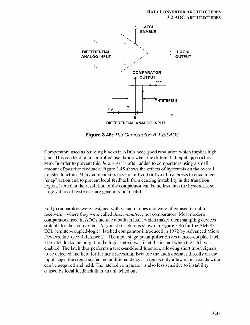
DATA CONVERTER ARCHITECTURES 3.2 ADC ARCHITECTURES
3.43
Figure 3.45: The Comparator: A 1-Bit ADC
Comparators used as building blocks in ADCs need good resolution which implies high gain. This can lead to uncontrolled oscillation when the differential input approaches zero. In order to prevent this, hysteresis is often added to comparators using a small amount of positive feedback. Figure 3.45 shows the effects of hysteresis on the overall transfer function. Many comparators have a millivolt or two of hysteresis to encourage "snap" action and to prevent local feedback from causing instability in the transition region. Note that the resolution of the comparator can be no less than the hysteresis, so large values of hysteresis are generally not useful. Early comparators were designed with vacuum tubes and were often used in radio receivers—where they were called discriminators, not comparators. Most modern comparators used in ADCs include a built-in latch which makes them sampling devices suitable for data converters. A typical structure is shown in Figure 3.46 for the AM685 ECL (emitter-coupled-logic) latched comparator introduced in 1972 by Advanced Micro Devices, Inc. (see Reference 2). The input stage preamplifier drives a cross-coupled latch. The latch locks the output in the logic state it was in at the instant when the latch was enabled. The latch thus performs a track-and-hold function, allowing short input signals to be detected and held for further processing. Because the latch operates directly on the input stage, the signal suffers no additional delays—signals only a few nanoseconds wide can be acquired and held. The latched comparator is also less sensitive to instability caused by local feedback than an unlatched one.
+
–
DIFFERENTIALANALOG INPUT
LOGICOUTPUT
LATCHENABLE
DIFFERENTIAL ANALOG INPUT
COMPARATOR OUTPUT
"0"
"1"
0
VHYSTERESIS
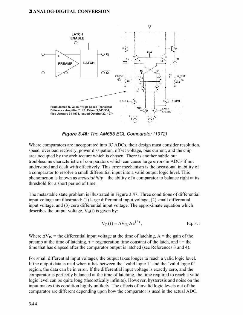
ANALOG-DIGITAL CONVERSION
3.44
Figure 3.46: The AM685 ECL Comparator (1972)
Where comparators are incorporated into IC ADCs, their design must consider resolution, speed, overload recovery, power dissipation, offset voltage, bias current, and the chip area occupied by the architecture which is chosen. There is another subtle but troublesome characteristic of comparators which can cause large errors in ADCs if not understood and dealt with effectively. This error mechanism is the occasional inability of a comparator to resolve a small differential input into a valid output logic level. This phenomenon is known as metastability—the ability of a comparator to balance right at its threshold for a short period of time. The metastable state problem is illustrated in Figure 3.47. Three conditions of differential input voltage are illustrated: (1) large differential input voltage, (2) small differential input voltage, and (3) zero differential input voltage. The approximate equation which describes the output voltage, VO(t) is given by:
τ∆= /tINO AeV)t(V , Eq. 3.1
Where ∆VIN = the differential input voltage at the time of latching, A = the gain of the preamp at the time of latching, τ = regeneration time constant of the latch, and t = the time that has elapsed after the comparator output is latched (see References 3 and 4). For small differential input voltages, the output takes longer to reach a valid logic level. If the output data is read when it lies between the "valid logic 1" and the "valid logic 0" region, the data can be in error. If the differential input voltage is exactly zero, and the comparator is perfectly balanced at the time of latching, the time required to reach a valid logic level can be quite long (theoretically infinite). However, hysteresis and noise on the input makes this condition highly unlikely. The effects of invalid logic levels out of the comparator are different depending upon how the comparator is used in the actual ADC.
+
–
PREAMP
Q
Q
LATCH
LATCHENABLE
From James N. Giles, "High Speed TransistorDifference Amplifier," U.S. Patent 3,843,934,filed January 31 1973, issued October 22, 1974
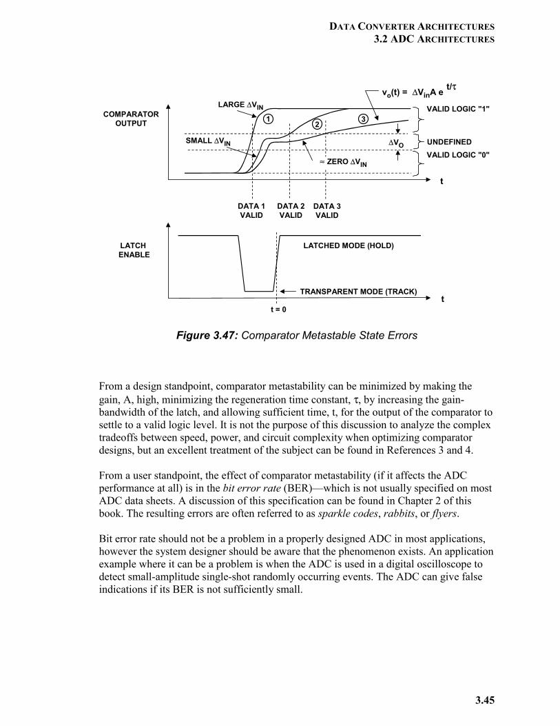
DATA CONVERTER ARCHITECTURES 3.2 ADC ARCHITECTURES
3.45
Figure 3.47: Comparator Metastable State Errors
From a design standpoint, comparator metastability can be minimized by making the gain, A, high, minimizing the regeneration time constant, τ, by increasing the gain-bandwidth of the latch, and allowing sufficient time, t, for the output of the comparator to settle to a valid logic level. It is not the purpose of this discussion to analyze the complex tradeoffs between speed, power, and circuit complexity when optimizing comparator designs, but an excellent treatment of the subject can be found in References 3 and 4. From a user standpoint, the effect of comparator metastability (if it affects the ADC performance at all) is in the bit error rate (BER)—which is not usually specified on most ADC data sheets. A discussion of this specification can be found in Chapter 2 of this book. The resulting errors are often referred to as sparkle codes, rabbits, or flyers. Bit error rate should not be a problem in a properly designed ADC in most applications, however the system designer should be aware that the phenomenon exists. An application example where it can be a problem is when the ADC is used in a digital oscilloscope to detect small-amplitude single-shot randomly occurring events. The ADC can give false indications if its BER is not sufficiently small.
t
t
LATCHENABLE
COMPARATOROUTPUT
VALID LOGIC "1"
VALID LOGIC "0"
LARGE ∆VIN
SMALL ∆VIN
12
DATA 1VALID
DATA 2VALID
UNDEFINED
TRANSPARENT MODE (TRACK)
LATCHED MODE (HOLD)
3
≈ ZERO ∆VIN
DATA 3VALID
∆VO
vo(t) = ∆VinA e t/τ
t = 0
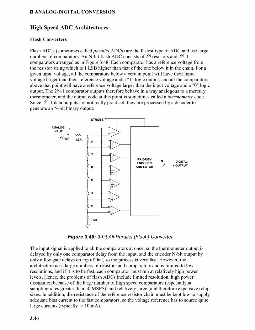
ANALOG-DIGITAL CONVERSION
3.46
High Speed ADC Architectures Flash Converters Flash ADCs (sometimes called parallel ADCs) are the fastest type of ADC and use large numbers of comparators. An N-bit flash ADC consists of 2N resistors and 2N–1 comparators arranged as in Figure 3.48. Each comparator has a reference voltage from the resistor string which is 1 LSB higher than that of the one below it in the chain. For a given input voltage, all the comparators below a certain point will have their input voltage larger than their reference voltage and a "1" logic output, and all the comparators above that point will have a reference voltage larger than the input voltage and a "0" logic output. The 2N–1 comparator outputs therefore behave in a way analogous to a mercury thermometer, and the output code at this point is sometimes called a thermometer code. Since 2N–1 data outputs are not really practical, they are processed by a decoder to generate an N-bit binary output.
Figure 3.48: 3-bit All-Parallel (Flash) Converter
The input signal is applied to all the comparators at once, so the thermometer output is delayed by only one comparator delay from the input, and the encoder N-bit output by only a few gate delays on top of that, so the process is very fast. However, the architecture uses large numbers of resistors and comparators and is limited to low resolutions, and if it is to be fast, each comparator must run at relatively high power levels. Hence, the problems of flash ADCs include limited resolution, high power dissipation because of the large number of high speed comparators (especially at sampling rates greater than 50 MSPS), and relatively large (and therefore expensive) chip sizes. In addition, the resistance of the reference resistor chain must be kept low to supply adequate bias current to the fast comparators, so the voltage reference has to source quite large currents (typically > 10 mA).
N
R
PRIORITYENCODER
AND LATCH
ANALOGINPUT
DIGITALOUTPUT
+VREF
R
R
R
R
R
0.5R
STROBE
1.5R
+
–
+
–
+
+
+
+
+
–
–
–
–
–
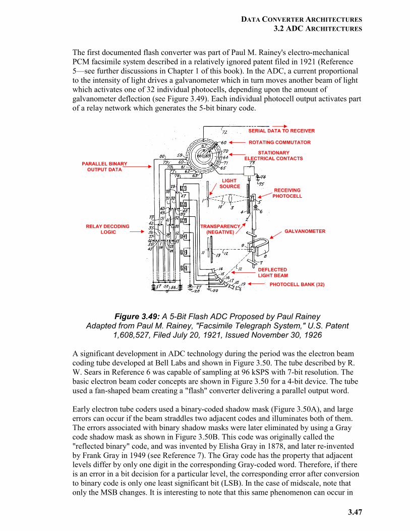
DATA CONVERTER ARCHITECTURES 3.2 ADC ARCHITECTURES
3.47
The first documented flash converter was part of Paul M. Rainey's electro-mechanical PCM facsimile system described in a relatively ignored patent filed in 1921 (Reference 5—see further discussions in Chapter 1 of this book). In the ADC, a current proportional to the intensity of light drives a galvanometer which in turn moves another beam of light which activates one of 32 individual photocells, depending upon the amount of galvanometer deflection (see Figure 3.49). Each individual photocell output activates part of a relay network which generates the 5-bit binary code.
Figure 3.49: A 5-Bit Flash ADC Proposed by Paul Rainey Adapted from Paul M. Rainey, "Facsimile Telegraph System," U.S. Patent
1,608,527, Filed July 20, 1921, Issued November 30, 1926 A significant development in ADC technology during the period was the electron beam coding tube developed at Bell Labs and shown in Figure 3.50. The tube described by R. W. Sears in Reference 6 was capable of sampling at 96 kSPS with 7-bit resolution. The basic electron beam coder concepts are shown in Figure 3.50 for a 4-bit device. The tube used a fan-shaped beam creating a "flash" converter delivering a parallel output word. Early electron tube coders used a binary-coded shadow mask (Figure 3.50A), and large errors can occur if the beam straddles two adjacent codes and illuminates both of them. The errors associated with binary shadow masks were later eliminated by using a Gray code shadow mask as shown in Figure 3.50B. This code was originally called the "reflected binary" code, and was invented by Elisha Gray in 1878, and later re-invented by Frank Gray in 1949 (see Reference 7). The Gray code has the property that adjacent levels differ by only one digit in the corresponding Gray-coded word. Therefore, if there is an error in a bit decision for a particular level, the corresponding error after conversion to binary code is only one least significant bit (LSB). In the case of midscale, note that only the MSB changes. It is interesting to note that this same phenomenon can occur in
TRANSPARENCY(NEGATIVE)
DEFLECTEDLIGHT BEAM
PHOTOCELL BANK (32)
SERIAL DATA TO RECEIVER
RECEIVINGPHOTOCELL
RELAY DECODING LOGIC
PARALLEL BINARYOUTPUT DATA
LIGHT SOURCE
GALVANOMETER
ROTATING COMMUTATOR
STATIONARYELECTRICAL CONTACTS
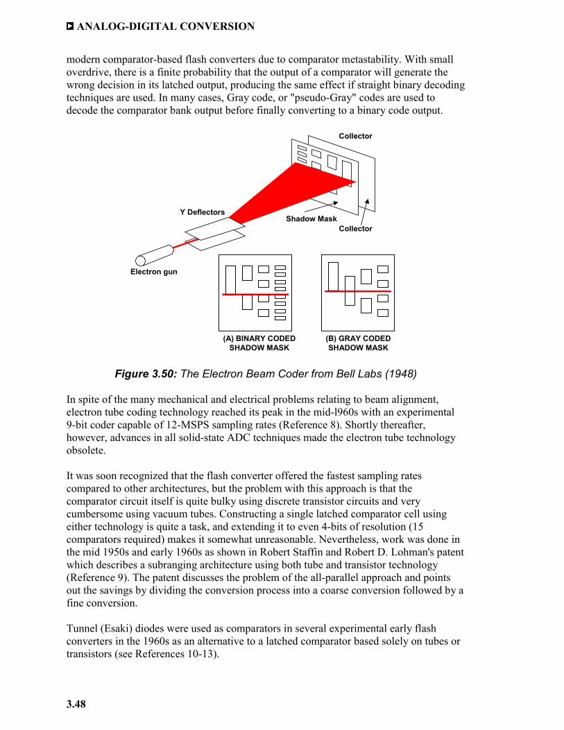
ANALOG-DIGITAL CONVERSION
3.48
modern comparator-based flash converters due to comparator metastability. With small overdrive, there is a finite probability that the output of a comparator will generate the wrong decision in its latched output, producing the same effect if straight binary decoding techniques are used. In many cases, Gray code, or "pseudo-Gray" codes are used to decode the comparator bank output before finally converting to a binary code output.
Figure 3.50: The Electron Beam Coder from Bell Labs (1948)
In spite of the many mechanical and electrical problems relating to beam alignment, electron tube coding technology reached its peak in the mid-l960s with an experimental 9-bit coder capable of 12-MSPS sampling rates (Reference 8). Shortly thereafter, however, advances in all solid-state ADC techniques made the electron tube technology obsolete. It was soon recognized that the flash converter offered the fastest sampling rates compared to other architectures, but the problem with this approach is that the comparator circuit itself is quite bulky using discrete transistor circuits and very cumbersome using vacuum tubes. Constructing a single latched comparator cell using either technology is quite a task, and extending it to even 4-bits of resolution (15 comparators required) makes it somewhat unreasonable. Nevertheless, work was done in the mid 1950s and early 1960s as shown in Robert Staffin and Robert D. Lohman's patent which describes a subranging architecture using both tube and transistor technology (Reference 9). The patent discusses the problem of the all-parallel approach and points out the savings by dividing the conversion process into a coarse conversion followed by a fine conversion. Tunnel (Esaki) diodes were used as comparators in several experimental early flash converters in the 1960s as an alternative to a latched comparator based solely on tubes or transistors (see References 10-13).
Electron gun
Collector
Y DeflectorsShadow Mask
Collector
(A) BINARY CODEDSHADOW MASK
(B) GRAY CODEDSHADOW MASK
DATA CONVERTER ARCHITECTURES 3.2 ADC ARCHITECTURES
3.49
In 1964 Fairchild introduced the first IC comparators, the µA711/712, designed by Bob Widlar. The same year, Fairchild also introduced the first IC op amp, the µA709—another Widlar design. Other IC comparators soon followed including the Signetics 521, National LM361, Motorola MC1650 (1968), AM685/687 (1972/1975). With the introduction of these building block comparators and the availability of TTL and ECL logic ICs, 6-bit rack-mounted discrete flash converters were introduced by Computer Labs, Inc., including the VHS-630 (6-bit, 30 MSPS in 1970) and the VHS-675 (6-bit, 75 MSPS in 1975). The VHS-675 shown in Figure 3.51 used 63 AM685 ECL comparators preceded by a high-speed track-and-hold, ECL decoding logic, contained a built-in linear power supply (ac line powered), and dissipated a total of 130 W (sale price was about $10,000 in 1975). Instruments such as these found application in early high speed data acquisition applications including military radar receivers.
Figure 3.51: VHS-Series ADCs from Computer Labs, Inc.
VHS-630 (1970), VHS-675 (1975) The AM685 comparator was also used as a building block in the 4-bit 100-MSPS board-level flash ADC, the MOD-4100, introduced in 1975 and shown in Figure 3.52. The first integrated circuit 8-bit video-speed 30-MSPS flash converter, the TDC1007J, was introduced by TRW LSI division in 1979 (References 14 and 15). A 6-bit version of the same design, the TDC1014J followed shortly. Also in 1979, Advanced Micro Devices, Inc. introduced the AM6688, a 4-bit 100-MSPS IC flash converter. Flash converters became very popular in the 1980s for high speed 8-bit video applications as well as building blocks for higher resolution subranging card-level, modular, and hybrid ADCs. Many were fabricated on CMOS processes for lower power dissipation. Recently, however, the subranging pipeline architecture has become popular for 8-bit ADCs up to about 250 MSPS. For instance, the AD9480 8-bit 250-MSPS ADC is fabricated on a high speed BiCMOS process and dissipates less than 400mW compared to the several watts required for a full flash implementation on a similar process.
VHS-6306-Bits, 30 MSPS32 dual MC1650 MECL III Comparators100 watts (linear powersupplies included)
VHS-6756-Bits, 75 MSPS64 AM685 Comparators130 watts (linear powersupplies included)
19" × 17" × 7"
ANALOG-DIGITAL CONVERSION
3.50
Figure 3.52: MOD-4100 4-Bit, 100-MSPS Flash Converter,
Computer Labs, 1975 In practice, IC flash converters are currently available up to 10-bits, but more commonly they have 8-bits of resolution. Their maximum sampling rate can be as high as 1 GHz (these are generally made on Gallium Arsenide processes with several watts of power dissipation), with input full-power bandwidths in excess of 300 MHz. But as mentioned earlier, full-power bandwidths are not necessarily full-resolution bandwidths. Ideally, the comparators in a flash converter are well matched both for dc and ac characteristics. Because the sampling clock is applied to all the comparators simultaneously, the flash converter is inherently a sampling converter. In practice, there are delay variations between the comparators and other ac mismatches which cause a degradation in the effective number of bits (ENOBs) at high input frequencies. This is because the inputs are slewing at a rate comparable to the comparator conversion time. For this reason, track-and-holds are often required ahead of flash converters to achieve high SFDR on high frequency input signals. The input to a flash ADC is applied in parallel to a large number of comparators. Each has a voltage-variable junction capacitance, and this signal-dependent capacitance results in most flash ADCs having reduced ENOB and higher distortion at high input frequencies. For this reason, most flash converters must be driven with a wideband op amp which is tolerant to the capacitive load presented by the converter as well as high speed transients developed on the input. Comparator metastability in a flash converter can severely impact the bit error rate (BER). Figure 3.53 shows a simple flash converter with one stage of binary decoding logic. The two-input AND gates convert the thermometer code output of the parallel comparators into a "one-hot out of 7" code. The decoding logic is simply a "wired-or"
AM685 ECL COMPARATORS(16 TOTAL)
14 watts total
9" × 6" × 2"
DATA CONVERTER ARCHITECTURES 3.2 ADC ARCHITECTURES
3.51
array, a technique popular with ECL logic. Assume that the comparator labeled "X" has metastable outputs labeled "X". The desired output code should be either 011 or 100, but note that the 000 code (both gate outputs high) and the 111 code (both gate outputs low) are also possible due to the metastable states, representing a ½ FS error.
Figure 3.53: Metastable Comparator Output States May Cause Error Codes in Data Converters
Metastable state errors in flash converters can be reduced by several techniques, one of which involves decoding the comparator outputs in Gray code followed by a Gray-to-binary conversion as in the Bell Labs electron beam encoder previously described. The advantage of Gray code decoding is that a metastable state in any of the comparators can produce only a 1-LSB error in the Gray code output. The Gray code is latched and then converted into a binary code which, in turn, will only have a maximum of 1-LSB error as shown in Figure 3.54. (This is described in more detail in Chapter 1 of this book in the section on coding). The same principles have been applied to several modern IC flash converters to minimize the effects of metastable state errors as described in References 3, 16, 17, for example. Power dissipation is always a big consideration in flash converters, especially at resolutions above 8 bits. A clever technique was used in the AD9410 10-bit, 210-MSPS ADC called interpolation to minimize the number of preamplifiers in the flash converter comparators and also reduce the power (2.1 W). The method is shown in Figure 3.55 (see Reference 18).
ANALOGINPUT
ANALOGINPUT
ANALOG-DIGITAL CONVERSION
3.52
Figure 3.54: Gray Code Decoding Reduces
Amplitude of Metastable State Errors
Figure 3.55: "Interpolating" Flash Reduces the Number of Preamplifiers by Factor of Two
B
V1A =
A2
LATCHSTROBE
ANALOGINPUT ANALOG
INPUT
DECODE
LATCH2
LATCH1A
LATCH1
A
B
V2
V1 AA1
+
+
-
-
B
B
B
B
V1A
V1
A
A
A
A
V2
V1 + V22
AD9410: 10-Bits, 210MSPS
1 1 1 11 1 1 01 1 0 11 1 0 01 0 1 11 0 1 01 0 0 11 0 0 00 1 1 10 1 1 00 1 0 10 1 0 00 0 1 10 0 1 00 0 0 10 0 0 0
1 0 0 01 0 0 11 0 1 11 0 1 01 1 1 01 1 1 11 1 0 11 1 0 00 1 0 00 1 0 10 1 1 10 1 1 00 0 1 00 0 1 10 0 0 10 0 0 0
(B) AFTER CONVERSIONTO BINARY CODE
(A) 4-BIT GRAY CODE
1 1 0 0
0 1 0 0
ONLY ONE BITCHANGES BETWEENANY TWO ADJACENT
CODES
METASTABLE STATEERROR PRODUCESONLY ONE OF TWO
POSSIBLE GRAY CODES
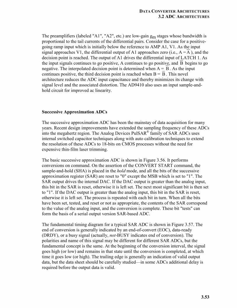
DATA CONVERTER ARCHITECTURES 3.2 ADC ARCHITECTURES
3.53
The preamplifiers (labeled "A1", "A2", etc.) are low-gain gm stages whose bandwidth is proportional to the tail currents of the differential pairs. Consider the case for a positive-going ramp input which is initially below the reference to AMP A1, V1. As the input signal approaches V1, the differential output of A1 approaches zero (i.e., A = A ), and the decision point is reached. The output of A1 drives the differential input of LATCH 1. As the input signals continues to go positive, A continues to go positive, and B begins to go negative. The interpolated decision point is determined when A = B . As the input continues positive, the third decision point is reached when B = B . This novel architecture reduces the ADC input capacitance and thereby minimizes its change with signal level and the associated distortion. The AD9410 also uses an input sample-and-hold circuit for improved ac linearity. Successive Approximation ADCs The successive approximation ADC has been the mainstay of data acquisition for many years. Recent design improvements have extended the sampling frequency of these ADCs into the megahertz region. The Analog Devices PulSAR® family of SAR ADCs uses internal switched capacitor techniques along with auto calibration techniques to extend the resolution of these ADCs to 18-bits on CMOS processes without the need for expensive thin-film laser trimming. The basic successive approximation ADC is shown in Figure 3.56. It performs conversions on command. On the assertion of the CONVERT START command, the sample-and-hold (SHA) is placed in the hold mode, and all the bits of the successive approximation register (SAR) are reset to "0" except the MSB which is set to "1". The SAR output drives the internal DAC. If the DAC output is greater than the analog input, this bit in the SAR is reset, otherwise it is left set. The next most significant bit is then set to "1". If the DAC output is greater than the analog input, this bit in the SAR is reset, otherwise it is left set. The process is repeated with each bit in turn. When all the bits have been set, tested, and reset or not as appropriate, the contents of the SAR correspond to the value of the analog input, and the conversion is complete. These bit "tests" can form the basis of a serial output version SAR-based ADC. The fundamental timing diagram for a typical SAR ADC is shown in Figure 3.57. The end of conversion is generally indicated by an end-of-convert (EOC), data-ready (DRDY), or a busy signal (actually, not-BUSY indicates end of conversion). The polarities and name of this signal may be different for different SAR ADCs, but the fundamental concept is the same. At the beginning of the conversion interval, the signal goes high (or low) and remains in that state until the conversion is completed, at which time it goes low (or high). The trailing edge is generally an indication of valid output data, but the data sheet should be carefully studied—in some ADCs additional delay is required before the output data is valid.
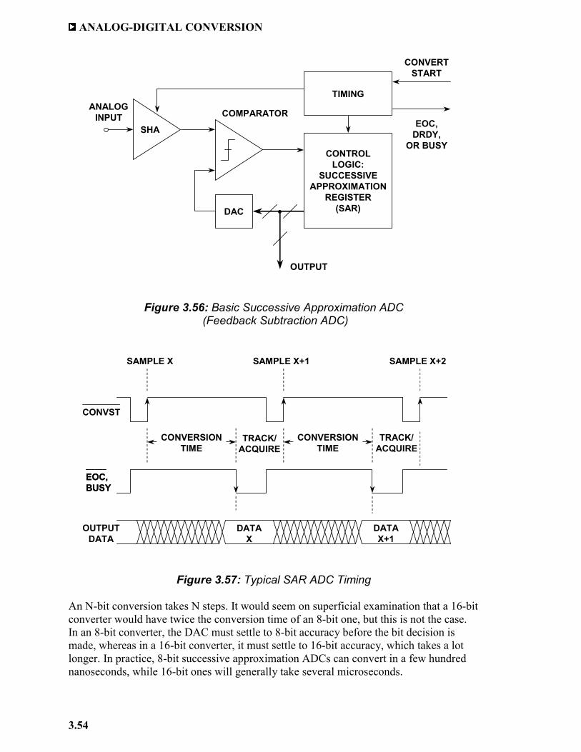
ANALOG-DIGITAL CONVERSION
3.54
Figure 3.56: Basic Successive Approximation ADC (Feedback Subtraction ADC)
Figure 3.57: Typical SAR ADC Timing An N-bit conversion takes N steps. It would seem on superficial examination that a 16-bit converter would have twice the conversion time of an 8-bit one, but this is not the case. In an 8-bit converter, the DAC must settle to 8-bit accuracy before the bit decision is made, whereas in a 16-bit converter, it must settle to 16-bit accuracy, which takes a lot longer. In practice, 8-bit successive approximation ADCs can convert in a few hundred nanoseconds, while 16-bit ones will generally take several microseconds.
SHA
CONTROLLOGIC:
SUCCESSIVEAPPROXIMATION
REGISTER(SAR)DAC
TIMING
CONVERTSTART
EOC,DRDY,
OR BUSY
OUTPUT
ANALOGINPUT COMPARATOR
CONVST
CONVERSIONTIME
SAMPLE X SAMPLE X+1 SAMPLE X+2
DATAX
DATAX+1
OUTPUTDATA
EOC,BUSYEOC,BUSY
TRACK/ACQUIRE
CONVERSIONTIME
TRACK/ACQUIRE
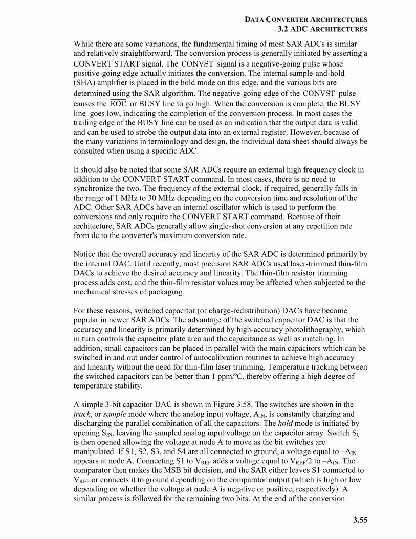
DATA CONVERTER ARCHITECTURES 3.2 ADC ARCHITECTURES
3.55
While there are some variations, the fundamental timing of most SAR ADCs is similar and relatively straightforward. The conversion process is generally initiated by asserting a CONVERT START signal. The CONVST signal is a negative-going pulse whose positive-going edge actually initiates the conversion. The internal sample-and-hold (SHA) amplifier is placed in the hold mode on this edge, and the various bits are determined using the SAR algorithm. The negative-going edge of the CONVST pulse causes the EOC or BUSY line to go high. When the conversion is complete, the BUSY line goes low, indicating the completion of the conversion process. In most cases the trailing edge of the BUSY line can be used as an indication that the output data is valid and can be used to strobe the output data into an external register. However, because of the many variations in terminology and design, the individual data sheet should always be consulted when using a specific ADC. It should also be noted that some SAR ADCs require an external high frequency clock in addition to the CONVERT START command. In most cases, there is no need to synchronize the two. The frequency of the external clock, if required, generally falls in the range of 1 MHz to 30 MHz depending on the conversion time and resolution of the ADC. Other SAR ADCs have an internal oscillator which is used to perform the conversions and only require the CONVERT START command. Because of their architecture, SAR ADCs generally allow single-shot conversion at any repetition rate from dc to the converter's maximum conversion rate. Notice that the overall accuracy and linearity of the SAR ADC is determined primarily by the internal DAC. Until recently, most precision SAR ADCs used laser-trimmed thin-film DACs to achieve the desired accuracy and linearity. The thin-film resistor trimming process adds cost, and the thin-film resistor values may be affected when subjected to the mechanical stresses of packaging. For these reasons, switched capacitor (or charge-redistribution) DACs have become popular in newer SAR ADCs. The advantage of the switched capacitor DAC is that the accuracy and linearity is primarily determined by high-accuracy photolithography, which in turn controls the capacitor plate area and the capacitance as well as matching. In addition, small capacitors can be placed in parallel with the main capacitors which can be switched in and out under control of autocalibration routines to achieve high accuracy and linearity without the need for thin-film laser trimming. Temperature tracking between the switched capacitors can be better than 1 ppm/ºC, thereby offering a high degree of temperature stability. A simple 3-bit capacitor DAC is shown in Figure 3.58. The switches are shown in the track, or sample mode where the analog input voltage, AIN, is constantly charging and discharging the parallel combination of all the capacitors. The hold mode is initiated by opening SIN, leaving the sampled analog input voltage on the capacitor array. Switch SC is then opened allowing the voltage at node A to move as the bit switches are manipulated. If S1, S2, S3, and S4 are all connected to ground, a voltage equal to –AIN appears at node A. Connecting S1 to VREF adds a voltage equal to VREF/2 to –AIN. The comparator then makes the MSB bit decision, and the SAR either leaves S1 connected to VREF or connects it to ground depending on the comparator output (which is high or low depending on whether the voltage at node A is negative or positive, respectively). A similar process is followed for the remaining two bits. At the end of the conversion
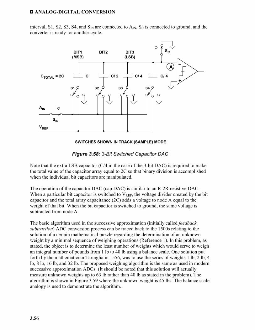
ANALOG-DIGITAL CONVERSION
3.56
interval, S1, S2, S3, S4, and SIN are connected to AIN, SC is connected to ground, and the converter is ready for another cycle.
Figure 3.58: 3-Bit Switched Capacitor DAC
Note that the extra LSB capacitor (C/4 in the case of the 3-bit DAC) is required to make the total value of the capacitor array equal to 2C so that binary division is accomplished when the individual bit capacitors are manipulated. The operation of the capacitor DAC (cap DAC) is similar to an R-2R resistive DAC. When a particular bit capacitor is switched to VREF, the voltage divider created by the bit capacitor and the total array capacitance (2C) adds a voltage to node A equal to the weight of that bit. When the bit capacitor is switched to ground, the same voltage is subtracted from node A. The basic algorithm used in the successive approximation (initially called feedback subtraction) ADC conversion process can be traced back to the 1500s relating to the solution of a certain mathematical puzzle regarding the determination of an unknown weight by a minimal sequence of weighing operations (Reference 1). In this problem, as stated, the object is to determine the least number of weights which would serve to weigh an integral number of pounds from 1 lb to 40 lb using a balance scale. One solution put forth by the mathematician Tartaglia in 1556, was to use the series of weights 1 lb, 2 lb, 4 lb, 8 lb, 16 lb, and 32 lb. The proposed weighing algorithm is the same as used in modern successive approximation ADCs. (It should be noted that this solution will actually measure unknown weights up to 63 lb rather than 40 lb as stated in the problem). The algorithm is shown in Figure 3.59 where the unknown weight is 45 lbs. The balance scale analogy is used to demonstrate the algorithm.
_
+
_
+C/ 4C/ 2C C/ 4
AIN
VREF
SIN
SC
S1 S2 S3 S4
BIT1(MSB)
BIT2 BIT3(LSB)
SWITCHES SHOWN IN TRACK (SAMPLE) MODE
AA
CTOTAL = 2C
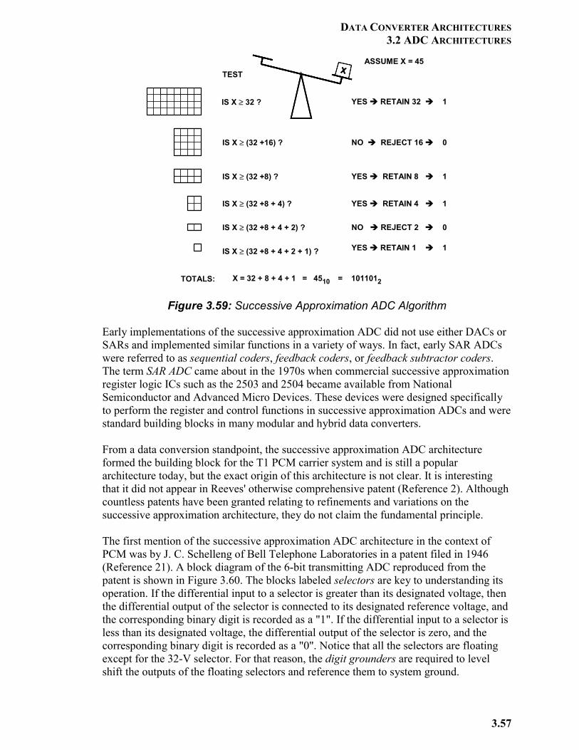
DATA CONVERTER ARCHITECTURES 3.2 ADC ARCHITECTURES
3.57
Figure 3.59: Successive Approximation ADC Algorithm
Early implementations of the successive approximation ADC did not use either DACs or SARs and implemented similar functions in a variety of ways. In fact, early SAR ADCs were referred to as sequential coders, feedback coders, or feedback subtractor coders. The term SAR ADC came about in the 1970s when commercial successive approximation register logic ICs such as the 2503 and 2504 became available from National Semiconductor and Advanced Micro Devices. These devices were designed specifically to perform the register and control functions in successive approximation ADCs and were standard building blocks in many modular and hybrid data converters. From a data conversion standpoint, the successive approximation ADC architecture formed the building block for the T1 PCM carrier system and is still a popular architecture today, but the exact origin of this architecture is not clear. It is interesting that it did not appear in Reeves' otherwise comprehensive patent (Reference 2). Although countless patents have been granted relating to refinements and variations on the successive approximation architecture, they do not claim the fundamental principle. The first mention of the successive approximation ADC architecture in the context of PCM was by J. C. Schelleng of Bell Telephone Laboratories in a patent filed in 1946 (Reference 21). A block diagram of the 6-bit transmitting ADC reproduced from the patent is shown in Figure 3.60. The blocks labeled selectors are key to understanding its operation. If the differential input to a selector is greater than its designated voltage, then the differential output of the selector is connected to its designated reference voltage, and the corresponding binary digit is recorded as a "1". If the differential input to a selector is less than its designated voltage, the differential output of the selector is zero, and the corresponding binary digit is recorded as a "0". Notice that all the selectors are floating except for the 32-V selector. For that reason, the digit grounders are required to level shift the outputs of the floating selectors and reference them to system ground.
XXXTEST
IS X ≥ 32 ? YES RETAIN 32 1
ASSUME X = 45
IS X ≥ (32 +16) ? NO REJECT 16 0
IS X ≥ (32 +8) ? YES RETAIN 8 1
IS X ≥ (32 +8 + 4) ? YES RETAIN 4 1
IS X ≥ (32 +8 + 4 + 2) ? NO REJECT 2 0
IS X ≥ (32 +8 + 4 + 2 + 1) ? YES RETAIN 1 1
X = 32 + 8 + 4 + 1 = 4510 = 1011012TOTALS:
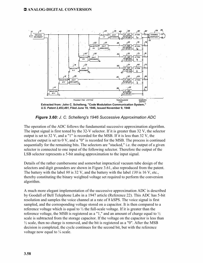
ANALOG-DIGITAL CONVERSION
3.58
Figure 3.60: J. C. Schelleng's 1946 Successive Approximation ADC
The operation of the ADC follows the fundamental successive approximation algorithm. The input signal is first tested by the 32-V selector. If it is greater than 32 V, the selector output is set to 32 V, and a "1" is recorded for the MSB. If it is less than 32 V, the selector output is set to 0 V, and a "0" is recorded for the MSB. The process is continued sequentially for the remaining bits. The selectors are "stacked," i.e. the output of a given selector is connected to one input of the following selector. Therefore the output of the LSB selector represents a 5-bit analog approximation to the input signal. Details of the rather cumbersome and somewhat impractical vacuum tube design of the selectors and digit grounders are shown in Figure 3.61, also reproduced from the patent. The battery with the label 98 is 32 V, and the battery with the label 130 is 16 V, etc., thereby constituting the binary weighted voltage set required to perform the conversion algorithm. A much more elegant implementation of the successive approximation ADC is described by Goodall of Bell Telephone Labs in a 1947 article (Reference 22). This ADC has 5-bit resolution and samples the voice channel at a rate of 8 kSPS. The voice signal is first sampled, and the corresponding voltage stored on a capacitor. It is then compared to a reference voltage which is equal to ½ the full-scale voltage. If it is greater than the reference voltage, the MSB is registered as a "1," and an amount of charge equal to ½ scale is subtracted from the storage capacitor. If the voltage on the capacitor is less than ½ scale, then no charge is removed, and the bit is registered as a "0". After the MSB decision is completed, the cycle continues for the second bit, but with the reference voltage now equal to ¼ scale.
Extracted from: John C. Schelleng, "Code Modulation Communication System,"U.S. Patent 2,453,461, Filed June 19, 1946, Issued November 9, 1948
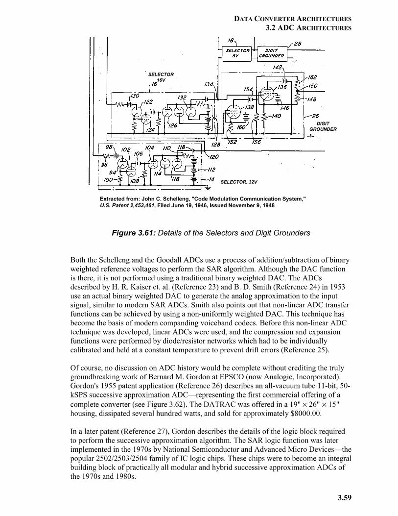
DATA CONVERTER ARCHITECTURES 3.2 ADC ARCHITECTURES
3.59
Figure 3.61: Details of the Selectors and Digit Grounders Both the Schelleng and the Goodall ADCs use a process of addition/subtraction of binary weighted reference voltages to perform the SAR algorithm. Although the DAC function is there, it is not performed using a traditional binary weighted DAC. The ADCs described by H. R. Kaiser et. al. (Reference 23) and B. D. Smith (Reference 24) in 1953 use an actual binary weighted DAC to generate the analog approximation to the input signal, similar to modern SAR ADCs. Smith also points out that non-linear ADC transfer functions can be achieved by using a non-uniformly weighted DAC. This technique has become the basis of modern companding voiceband codecs. Before this non-linear ADC technique was developed, linear ADCs were used, and the compression and expansion functions were performed by diode/resistor networks which had to be individually calibrated and held at a constant temperature to prevent drift errors (Reference 25). Of course, no discussion on ADC history would be complete without crediting the truly groundbreaking work of Bernard M. Gordon at EPSCO (now Analogic, Incorporated). Gordon's 1955 patent application (Reference 26) describes an all-vacuum tube 11-bit, 50-kSPS successive approximation ADC—representing the first commercial offering of a complete converter (see Figure 3.62). The DATRAC was offered in a 19" × 26" × 15" housing, dissipated several hundred watts, and sold for approximately $8000.00. In a later patent (Reference 27), Gordon describes the details of the logic block required to perform the successive approximation algorithm. The SAR logic function was later implemented in the 1970s by National Semiconductor and Advanced Micro Devices—the popular 2502/2503/2504 family of IC logic chips. These chips were to become an integral building block of practically all modular and hybrid successive approximation ADCs of the 1970s and 1980s.
SELECTOR, 32V
SELECTOR16V
DIGITGROUNDER
Extracted from: John C. Schelleng, "Code Modulation Communication System,"U.S. Patent 2,453,461, Filed June 19, 1946, Issued November 9, 1948
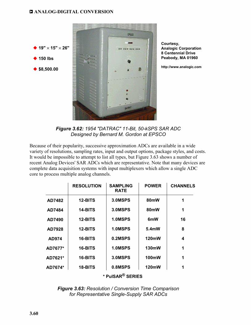
ANALOG-DIGITAL CONVERSION
3.60
Figure 3.62: 1954 "DATRAC" 11-Bit, 50-kSPS SAR ADC
Designed by Bernard M. Gordon at EPSCO Because of their popularity, successive approximation ADCs are available in a wide variety of resolutions, sampling rates, input and output options, package styles, and costs. It would be impossible to attempt to list all types, but Figure 3.63 shows a number of recent Analog Devices' SAR ADCs which are representative. Note that many devices are complete data acquisition systems with input multiplexers which allow a single ADC core to process multiple analog channels.
Figure 3.63: Resolution / Conversion Time Comparison
for Representative Single-Supply SAR ADCs
19" × 15" × 26"
150 lbs
$8,500.00
Courtesy,Analogic Corporation8 Centennial DrivePeabody, MA 01960
http://www.analogic.com
AD7482
AD7484
AD7490
AD7928
AD974
AD7677*
AD7621*
AD7674*
RESOLUTION
12-BITS
14-BITS
12-BITS
12-BITS
16-BITS
16-BITS
16-BITS
18-BITS
SAMPLINGRATE
3.0MSPS
3.0MSPS
1.0MSPS
1.0MSPS
0.2MSPS
1.0MSPS
3.0MSPS
0.8MSPS
POWER
80mW
80mW
6mW
5.4mW
120mW
130mW
100mW
120mW
CHANNELS
1
1
16
8
4
1
1
1
* PulSAR® SERIES
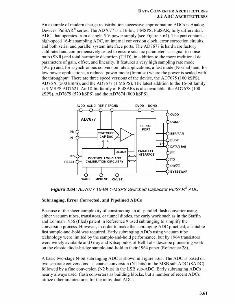
DATA CONVERTER ARCHITECTURES 3.2 ADC ARCHITECTURES
3.61
An example of modern charge redistribution successive approximation ADCs is Analog Devices' PulSAR series. The AD7677 is a 16-bit, 1-MSPS, PulSAR, fully differential, ADC that operates from a single 5 V power supply (see Figure 3.64). The part contains a high-speed 16-bit sampling ADC, an internal conversion clock, error correction circuits, and both serial and parallel system interface ports. The AD7677 is hardware factory calibrated and comprehensively tested to ensure such ac parameters as signal-to-noise ratio (SNR) and total harmonic distortion (THD), in addition to the more traditional dc parameters of gain, offset, and linearity. It features a very high sampling rate mode (Warp) and, for asynchronous conversion rate applications, a fast mode (Normal) and, for low power applications, a reduced power mode (Impulse) where the power is scaled with the throughput. There are three speed versions of the device, the AD7675 (100 kSPS), AD7676 (500 kSPS), and the AD7677 (1 MSPS). The latest addition to the 16-bit family is 3-MSPS AD7621. An 18-bit family of PulSARs is also available: the AD7678 (100 kSPS), AD7679 (570 kSPS) and the AD7674 (800 kSPS).
Figure 3.64: AD7677 16-Bit 1-MSPS Switched Capacitor PulSAR® ADC
Subranging, Error Corrected, and Pipelined ADCs Because of the sheer complexity of constructing an all-parallel flash converter using either vacuum tubes, transistors, or tunnel diodes, the early work such as in the Staffin and Lohman 1956 (filed) patent in Reference 9 used subranging to simplify the conversion process. However, in order to make the subranging ADC practical, a suitable fast sample-and-hold was required. Early subranging ADCs using vacuum tube technology were limited by the sample-and-hold performance, but by 1964 transistors were widely available and Gray and Kitsopoulos of Bell Labs describe pioneering work on the classic diode-bridge sample-and-hold in their 1964 paper (Reference 28). A basic two-stage N-bit subranging ADC is shown in Figure 3.65. The ADC is based on two separate conversions—a coarse conversion (N1 bits) in the MSB sub-ADC (SADC) followed by a fine conversion (N2 bits) in the LSB sub-ADC. Early subranging ADCs nearly always used flash converters as building blocks, but a number of recent ADCs utilize other architectures for the individual ADCs.
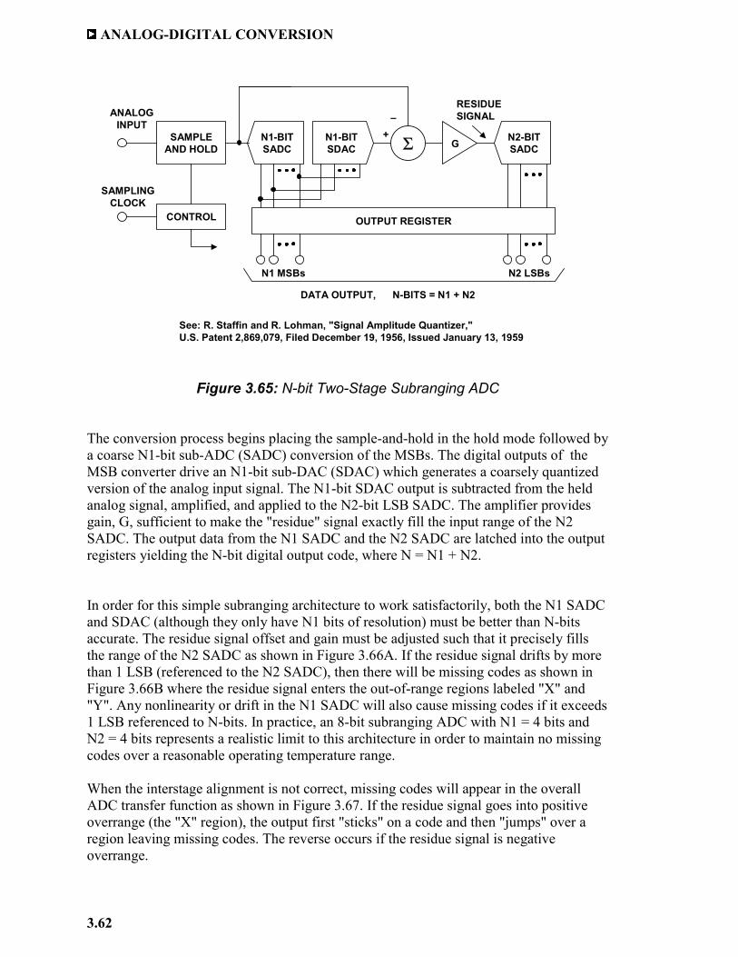
ANALOG-DIGITAL CONVERSION
3.62
Figure 3.65: N-bit Two-Stage Subranging ADC The conversion process begins placing the sample-and-hold in the hold mode followed by a coarse N1-bit sub-ADC (SADC) conversion of the MSBs. The digital outputs of the MSB converter drive an N1-bit sub-DAC (SDAC) which generates a coarsely quantized version of the analog input signal. The N1-bit SDAC output is subtracted from the held analog signal, amplified, and applied to the N2-bit LSB SADC. The amplifier provides gain, G, sufficient to make the "residue" signal exactly fill the input range of the N2 SADC. The output data from the N1 SADC and the N2 SADC are latched into the output registers yielding the N-bit digital output code, where N = N1 + N2. In order for this simple subranging architecture to work satisfactorily, both the N1 SADC and SDAC (although they only have N1 bits of resolution) must be better than N-bits accurate. The residue signal offset and gain must be adjusted such that it precisely fills the range of the N2 SADC as shown in Figure 3.66A. If the residue signal drifts by more than 1 LSB (referenced to the N2 SADC), then there will be missing codes as shown in Figure 3.66B where the residue signal enters the out-of-range regions labeled "X" and "Y". Any nonlinearity or drift in the N1 SADC will also cause missing codes if it exceeds 1 LSB referenced to N-bits. In practice, an 8-bit subranging ADC with N1 = 4 bits and N2 = 4 bits represents a realistic limit to this architecture in order to maintain no missing codes over a reasonable operating temperature range. When the interstage alignment is not correct, missing codes will appear in the overall ADC transfer function as shown in Figure 3.67. If the residue signal goes into positive overrange (the "X" region), the output first "sticks" on a code and then "jumps" over a region leaving missing codes. The reverse occurs if the residue signal is negative overrange.
SAMPLEAND HOLD Σ
+–
OUTPUT REGISTER
ANALOGINPUT
DATA OUTPUT, N-BITS = N1 + N2
CONTROL
SAMPLINGCLOCK
See: R. Staffin and R. Lohman, "Signal Amplitude Quantizer,"U.S. Patent 2,869,079, Filed December 19, 1956, Issued January 13, 1959
RESIDUESIGNAL
N1 MSBs N2 LSBs
GN1-BITSADC
N1-BITSDAC
N2-BITSADC
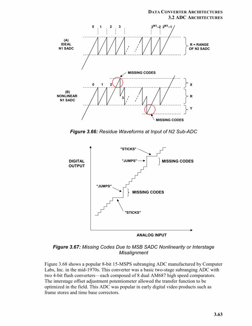
DATA CONVERTER ARCHITECTURES 3.2 ADC ARCHITECTURES
3.63
Figure 3.66: Residue Waveforms at Input of N2 Sub-ADC
Figure 3.67: Missing Codes Due to MSB SADC Nonlinearity or Interstage
Misalignment Figure 3.68 shows a popular 8-bit 15-MSPS subranging ADC manufactured by Computer Labs, Inc. in the mid-1970s. This converter was a basic two-stage subranging ADC with two 4-bit flash converters—each composed of 8 dual AM687 high speed comparators. The interstage offset adjustment potentiometer allowed the transfer function to be optimized in the field. This ADC was popular in early digital video products such as frame stores and time base correctors.
0 1 2 3 2N1–12N1–2
MISSING CODES
MISSING CODES
R = RANGEOF N2 SADC
X
R
Y
(A)IDEAL
N1 SADC
(B)NONLINEAR
N1 SADC
0 1 2
3
ANALOG INPUT
DIGITALOUTPUT
MISSING CODES
MISSING CODES
"STICKS"
"JUMPS"
"JUMPS"
"STICKS"
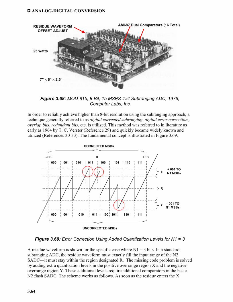
ANALOG-DIGITAL CONVERSION
3.64
Figure 3.68: MOD-815, 8-Bit, 15 MSPS 4×4 Subranging ADC, 1976,
Computer Labs, Inc. In order to reliably achieve higher than 8-bit resolution using the subranging approach, a technique generally referred to as digital corrected subranging, digital error correction, overlap bits, redundant bits, etc. is utilized. This method was referred to in literature as early as 1964 by T. C. Verster (Reference 29) and quickly became widely known and utilized (References 30-33). The fundamental concept is illustrated in Figure 3.69.
Figure 3.69: Error Correction Using Added Quantization Levels for N1 = 3
A residue waveform is shown for the specific case where N1 = 3 bits. In a standard subranging ADC, the residue waveform must exactly fill the input range of the N2 SADC—it must stay within the region designated R. The missing code problem is solved by adding extra quantization levels in the positive overrange region X and the negative overrange region Y. These additional levels require additional comparators in the basic N2 flash SADC. The scheme works as follows. As soon as the residue enters the X
000 001 010 011 100 101 110 111
R
X
Y
–FS +FS0
CORRECTED MSBs
+ 001 TON1 MSBs
– 001 TON1 MSBs
000 001 010 011 100 101 110 111
UNCORRECTED MSBs
25 watts
AM687 Dual Comparators (16 Total)RESIDUE WAVEFORMOFFSET ADJUST
7" × 6" × 2.5"
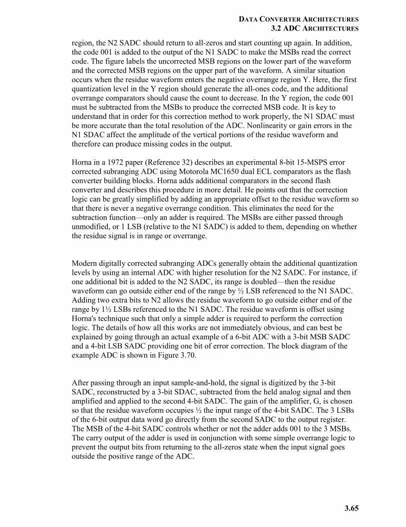
DATA CONVERTER ARCHITECTURES 3.2 ADC ARCHITECTURES
3.65
region, the N2 SADC should return to all-zeros and start counting up again. In addition, the code 001 is added to the output of the N1 SADC to make the MSBs read the correct code. The figure labels the uncorrected MSB regions on the lower part of the waveform and the corrected MSB regions on the upper part of the waveform. A similar situation occurs when the residue waveform enters the negative overrange region Y. Here, the first quantization level in the Y region should generate the all-ones code, and the additional overrange comparators should cause the count to decrease. In the Y region, the code 001 must be subtracted from the MSBs to produce the corrected MSB code. It is key to understand that in order for this correction method to work properly, the N1 SDAC must be more accurate than the total resolution of the ADC. Nonlinearity or gain errors in the N1 SDAC affect the amplitude of the vertical portions of the residue waveform and therefore can produce missing codes in the output. Horna in a 1972 paper (Reference 32) describes an experimental 8-bit 15-MSPS error corrected subranging ADC using Motorola MC1650 dual ECL comparators as the flash converter building blocks. Horna adds additional comparators in the second flash converter and describes this procedure in more detail. He points out that the correction logic can be greatly simplified by adding an appropriate offset to the residue waveform so that there is never a negative overrange condition. This eliminates the need for the subtraction function—only an adder is required. The MSBs are either passed through unmodified, or 1 LSB (relative to the N1 SADC) is added to them, depending on whether the residue signal is in range or overrange. Modern digitally corrected subranging ADCs generally obtain the additional quantization levels by using an internal ADC with higher resolution for the N2 SADC. For instance, if one additional bit is added to the N2 SADC, its range is doubled—then the residue waveform can go outside either end of the range by ½ LSB referenced to the N1 SADC. Adding two extra bits to N2 allows the residue waveform to go outside either end of the range by 1½ LSBs referenced to the N1 SADC. The residue waveform is offset using Horna's technique such that only a simple adder is required to perform the correction logic. The details of how all this works are not immediately obvious, and can best be explained by going through an actual example of a 6-bit ADC with a 3-bit MSB SADC and a 4-bit LSB SADC providing one bit of error correction. The block diagram of the example ADC is shown in Figure 3.70. After passing through an input sample-and-hold, the signal is digitized by the 3-bit SADC, reconstructed by a 3-bit SDAC, subtracted from the held analog signal and then amplified and applied to the second 4-bit SADC. The gain of the amplifier, G, is chosen so that the residue waveform occupies ½ the input range of the 4-bit SADC. The 3 LSBs of the 6-bit output data word go directly from the second SADC to the output register. The MSB of the 4-bit SADC controls whether or not the adder adds 001 to the 3 MSBs. The carry output of the adder is used in conjunction with some simple overrange logic to prevent the output bits from returning to the all-zeros state when the input signal goes outside the positive range of the ADC.
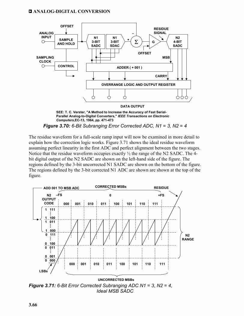
ANALOG-DIGITAL CONVERSION
3.66
Figure 3.70: 6-Bit Subranging Error Corrected ADC, N1 = 3, N2 = 4 The residue waveform for a full-scale ramp input will now be examined in more detail to explain how the correction logic works. Figure 3.71 shows the ideal residue waveform assuming perfect linearity in the first ADC and perfect alignment between the two stages. Notice that the residue waveform occupies exactly ½ the range of the N2 SADC. The 4-bit digital output of the N2 SADC are shown on the left-hand side of the figure. The regions defined by the 3-bit uncorrected N1 SADC are shown on the bottom of the figure. The regions defined by the 3-bit corrected N1 ADC are shown are shown at the top of the figure.
Figure 3.71: 6-Bit Error Corrected Subranging ADC N1 = 3, N2 = 4, Ideal MSB SADC
SAMPLEAND HOLD Σ+
–
OVERRANGE LOGIC AND OUTPUT REGISTER
ANALOGINPUT
DATA OUTPUT
CONTROL
SAMPLINGCLOCK
ADDER ( + 001 )
RESIDUESIGNAL
MSB
CARRY
G
SEE: T. C. Verster, "A Method to Increase the Accuracy of Fast Serial-Parallel Analog-to-Digital Converters," IEEE Transactions on Electronic Computers,EC-13, 1964, pp. 471-473
OFFSET
OFFSET
N13-BITSADC
N13-BITSDAC
N24-BITSADC
0 0010 000
0 1000 011
1 0000 111
1 1001 011
1 111000 001 010 011 100 101 110 111
N2RANGE
CORRECTED MSBs
N2OUTPUT
CODE
ADD 001 TO MSB ADC
–FS 0 +FS
RESIDUE
LSBs
000 001 010 011 100 101 110 111
UNCORRECTED MSBs
•••
•••
•••
•••
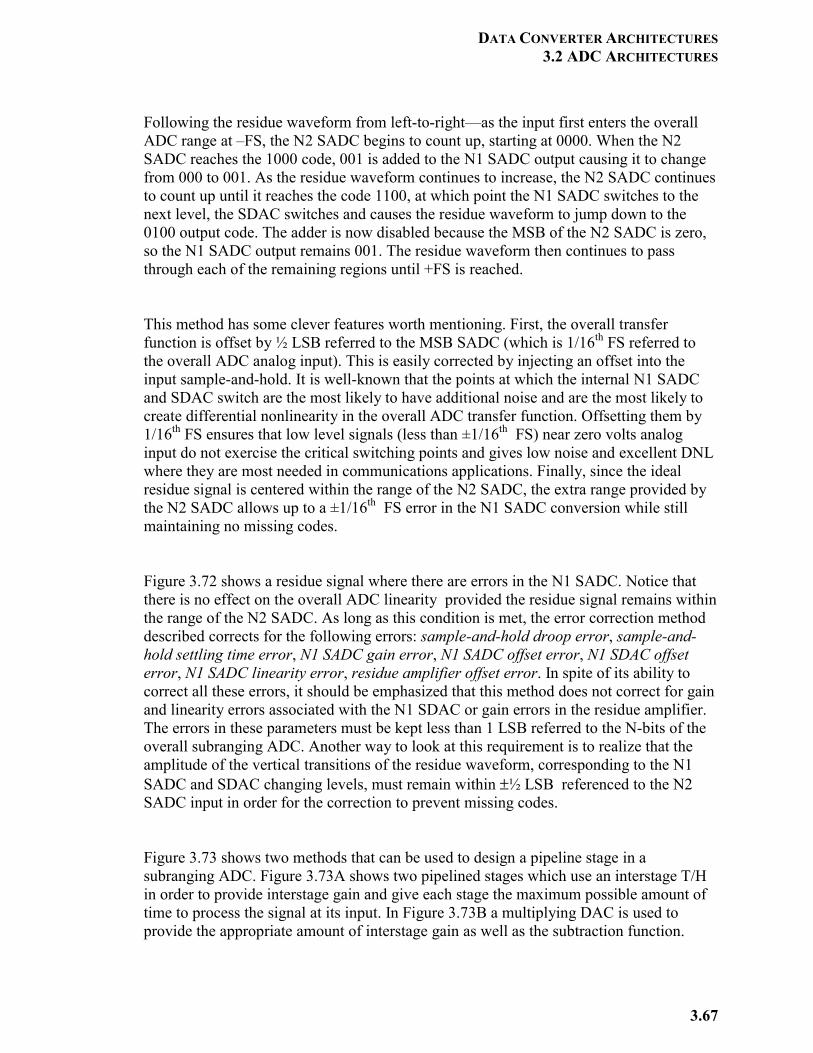
DATA CONVERTER ARCHITECTURES 3.2 ADC ARCHITECTURES
3.67
Following the residue waveform from left-to-right—as the input first enters the overall ADC range at –FS, the N2 SADC begins to count up, starting at 0000. When the N2 SADC reaches the 1000 code, 001 is added to the N1 SADC output causing it to change from 000 to 001. As the residue waveform continues to increase, the N2 SADC continues to count up until it reaches the code 1100, at which point the N1 SADC switches to the next level, the SDAC switches and causes the residue waveform to jump down to the 0100 output code. The adder is now disabled because the MSB of the N2 SADC is zero, so the N1 SADC output remains 001. The residue waveform then continues to pass through each of the remaining regions until +FS is reached. This method has some clever features worth mentioning. First, the overall transfer function is offset by ½ LSB referred to the MSB SADC (which is 1/16th FS referred to the overall ADC analog input). This is easily corrected by injecting an offset into the input sample-and-hold. It is well-known that the points at which the internal N1 SADC and SDAC switch are the most likely to have additional noise and are the most likely to create differential nonlinearity in the overall ADC transfer function. Offsetting them by 1/16th FS ensures that low level signals (less than ±1/16th FS) near zero volts analog input do not exercise the critical switching points and gives low noise and excellent DNL where they are most needed in communications applications. Finally, since the ideal residue signal is centered within the range of the N2 SADC, the extra range provided by the N2 SADC allows up to a ±1/16th FS error in the N1 SADC conversion while still maintaining no missing codes. Figure 3.72 shows a residue signal where there are errors in the N1 SADC. Notice that there is no effect on the overall ADC linearity provided the residue signal remains within the range of the N2 SADC. As long as this condition is met, the error correction method described corrects for the following errors: sample-and-hold droop error, sample-and-hold settling time error, N1 SADC gain error, N1 SADC offset error, N1 SDAC offset error, N1 SADC linearity error, residue amplifier offset error. In spite of its ability to correct all these errors, it should be emphasized that this method does not correct for gain and linearity errors associated with the N1 SDAC or gain errors in the residue amplifier. The errors in these parameters must be kept less than 1 LSB referred to the N-bits of the overall subranging ADC. Another way to look at this requirement is to realize that the amplitude of the vertical transitions of the residue waveform, corresponding to the N1 SADC and SDAC changing levels, must remain within ±½ LSB referenced to the N2 SADC input in order for the correction to prevent missing codes. Figure 3.73 shows two methods that can be used to design a pipeline stage in a subranging ADC. Figure 3.73A shows two pipelined stages which use an interstage T/H in order to provide interstage gain and give each stage the maximum possible amount of time to process the signal at its input. In Figure 3.73B a multiplying DAC is used to provide the appropriate amount of interstage gain as well as the subtraction function.
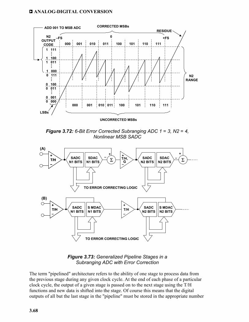
ANALOG-DIGITAL CONVERSION
3.68
Figure 3.72: 6-Bit Error Corrected Subranging ADC 1 = 3, N2 = 4,
Nonlinear MSB SADC
Figure 3.73: Generalized Pipeline Stages in a Subranging ADC with Error Correction
The term "pipelined" architecture refers to the ability of one stage to process data from the previous stage during any given clock cycle. At the end of each phase of a particular clock cycle, the output of a given stage is passed on to the next stage using the T/H functions and new data is shifted into the stage. Of course this means that the digital outputs of all but the last stage in the "pipeline" must be stored in the appropriate number
0 0010 000
0 1000 011
1 0000 111
1 1001 011
1 111000 001 010 011 100 101 110 111
N2RANGE
CORRECTED MSBs
N2OUTPUT
CODE
ADD 001 TO MSB ADCRESIDUE
–FS 0 +FS
LSBs
000 001 010 011 100 101 110 111
UNCORRECTED MSBs
•••
•••
•••
•••
SADCN1 BITS
SDACN1 BITST/H
+
–T/H+
–
+
–Σ
+– SADC
N2 BITSSDAC
N2 BITS Σ+
–
SADCN1 BITS
S MDACN1 BITST/H
+
–T/H+
–T/H+
–
SADCN2 BITS
S MDACN2 BITS
(A)
(B)
TO ERROR CORRECTING LOGIC
TO ERROR CORRECTING LOGIC
T/H,G
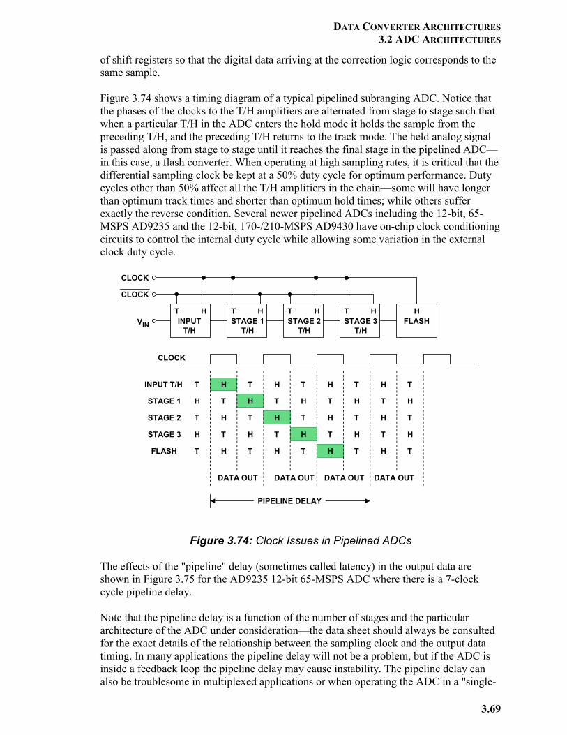
DATA CONVERTER ARCHITECTURES 3.2 ADC ARCHITECTURES
3.69
of shift registers so that the digital data arriving at the correction logic corresponds to the same sample. Figure 3.74 shows a timing diagram of a typical pipelined subranging ADC. Notice that the phases of the clocks to the T/H amplifiers are alternated from stage to stage such that when a particular T/H in the ADC enters the hold mode it holds the sample from the preceding T/H, and the preceding T/H returns to the track mode. The held analog signal is passed along from stage to stage until it reaches the final stage in the pipelined ADC—in this case, a flash converter. When operating at high sampling rates, it is critical that the differential sampling clock be kept at a 50% duty cycle for optimum performance. Duty cycles other than 50% affect all the T/H amplifiers in the chain—some will have longer than optimum track times and shorter than optimum hold times; while others suffer exactly the reverse condition. Several newer pipelined ADCs including the 12-bit, 65-MSPS AD9235 and the 12-bit, 170-/210-MSPS AD9430 have on-chip clock conditioning circuits to control the internal duty cycle while allowing some variation in the external clock duty cycle.
Figure 3.74: Clock Issues in Pipelined ADCs The effects of the "pipeline" delay (sometimes called latency) in the output data are shown in Figure 3.75 for the AD9235 12-bit 65-MSPS ADC where there is a 7-clock cycle pipeline delay. Note that the pipeline delay is a function of the number of stages and the particular architecture of the ADC under consideration—the data sheet should always be consulted for the exact details of the relationship between the sampling clock and the output data timing. In many applications the pipeline delay will not be a problem, but if the ADC is inside a feedback loop the pipeline delay may cause instability. The pipeline delay can also be troublesome in multiplexed applications or when operating the ADC in a "single-
FLASH
CLOCK
CLOCK
VIN
TINPUT
T/HSTAGE 1
T/HSTAGE 2
T/HSTAGE 3
T/H
H T H T H T H H
CLOCK
INPUT T/H
STAGE 1
STAGE 2
STAGE 3
FLASH
T H T H T H T H
H H T H T HT T
T H T H T H T H
H H T H T HT T
DATA OUT DATA OUT DATA OUT DATA OUT
T H T H T H T
H
T
H
T
H T
PIPELINE DELAY
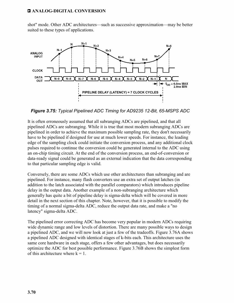
ANALOG-DIGITAL CONVERSION
3.70
shot" mode. Other ADC architectures—such as successive approximation—may be better suited to these types of applications.
Figure 3.75: Typical Pipelined ADC Timing for AD9235 12-Bit, 65-MSPS ADC
It is often erroneously assumed that all subranging ADCs are pipelined, and that all pipelined ADCs are subranging. While it is true that most modern subranging ADCs are pipelined in order to achieve the maximum possible sampling rate, they don't necessarily have to be pipelined if designed for use at much lower speeds. For instance, the leading edge of the sampling clock could initiate the conversion process, and any additional clock pulses required to continue the conversion could be generated internal to the ADC using an on-chip timing circuit. At the end of the conversion process, an end-of-conversion or data-ready signal could be generated as an external indication that the data corresponding to that particular sampling edge is valid. Conversely, there are some ADCs which use other architectures than subranging and are pipelined. For instance, many flash converters use an extra set of output latches (in addition to the latch associated with the parallel comparators) which introduces pipeline delay in the output data. Another example of a non-subranging architecture which generally has quite a bit of pipeline delay is sigma-delta which will be covered in more detail in the next section of this chapter. Note, however, that it is possible to modify the timing of a normal sigma-delta ADC, reduce the output data rate, and make a "no latency" sigma-delta ADC. The pipelined error correcting ADC has become very popular in modern ADCs requiring wide dynamic range and low levels of distortion. There are many possible ways to design a pipelined ADC, and we will now look at just a few of the tradeoffs. Figure 3.76A shows a pipelined ADC designed with identical stages of k-bits each. This architecture uses the same core hardware in each stage, offers a few other advantages, but does necessarily optimize the ADC for best possible performance. Figure 3.76B shows the simplest form of this architecture where k = 1.
PIPELINE DELAY (LATENCY) = 7 CLOCK CYCLES
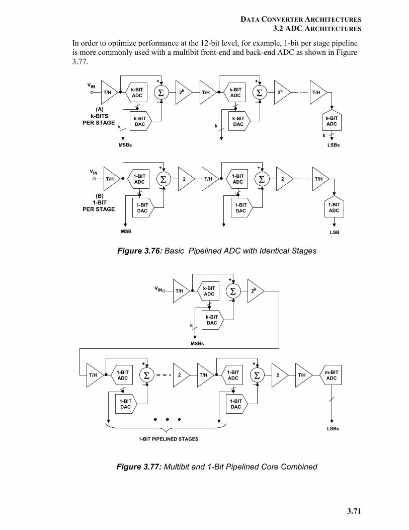
DATA CONVERTER ARCHITECTURES 3.2 ADC ARCHITECTURES
3.71
In order to optimize performance at the 12-bit level, for example, 1-bit per stage pipeline is more commonly used with a multibit front-end and back-end ADC as shown in Figure 3.77.
Figure 3.76: Basic Pipelined ADC with Identical Stages
Figure 3.77: Multibit and 1-Bit Pipelined Core Combined
T/H k-BITADC
k-BITDAC
Σ+
–
2k T/H k-BITADC
k-BITDAC
Σ+
–
2k T/H
k-BITADC
T/H 1-BITADC
1-BITDAC
Σ+
–
2 T/H 1-BITADC
1-BITDAC
Σ+
–
2 T/H
1-BITADC
k k
k
MSBs LSBs
MSB LSB
(A)k-BITS
PER STAGE
(B)1-BIT
PER STAGE
VIN
VIN
T/H k-BITADC
k-BITDAC
Σ+
–
2k
T/H 1-BITADC
1-BITDAC
Σ+
–
2 T/H
k
MSBs
T/H 1-BITADC
1-BITDAC
Σ+
–
2 m-BITADC
LSBs
1-BIT PIPELINED STAGES
VIN
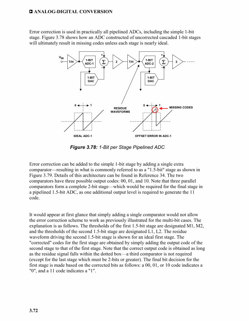
ANALOG-DIGITAL CONVERSION
3.72
Error correction is used in practically all pipelined ADCs, including the simple 1-bit stage. Figure 3.78 shows how an ADC constructed of uncorrected cascaded 1-bit stages will ultimately result in missing codes unless each stage is nearly ideal.
Figure 3.78: 1-Bit per Stage Pipelined ADC
Error correction can be added to the simple 1-bit stage by adding a single extra comparator—resulting in what is commonly referred to as a "1.5-bit" stage as shown in Figure 3.79. Details of this architecture can be found in Reference 34. The two comparators have three possible output codes: 00, 01, and 10. Note that three parallel comparators form a complete 2-bit stage—which would be required for the final stage in a pipelined 1.5-bit ADC, as one additional output level is required to generate the 11 code. It would appear at first glance that simply adding a single comparator would not allow the error correction scheme to work as previously illustrated for the multi-bit cases. The explanation is as follows. The thresholds of the first 1.5-bit stage are designated M1, M2, and the thresholds of the second 1.5-bit stage are designated L1, L2. The residue waveform driving the second 1.5-bit stage is shown for an ideal first stage. The "corrected" codes for the first stage are obtained by simply adding the output code of the second stage to that of the first stage. Note that the correct output code is obtained as long as the residue signal falls within the dotted box—a third comparator is not required (except for the last stage which must be 2-bits or greater). The final bit decision for the first stage is made based on the corrected bits as follows: a 00, 01, or 10 code indicates a "0", and a 11 code indicates a "1".
T/H 1-BITADC-1
1-BITDAC
Σ+
–
2 T/HVIN
RESIDUEWAVEFORMS
10 10MISSING CODES
1-BITADC-2
1-BITDAC
Σ+
–
2
IDEAL ADC-1 OFFSET ERROR IN ADC-1
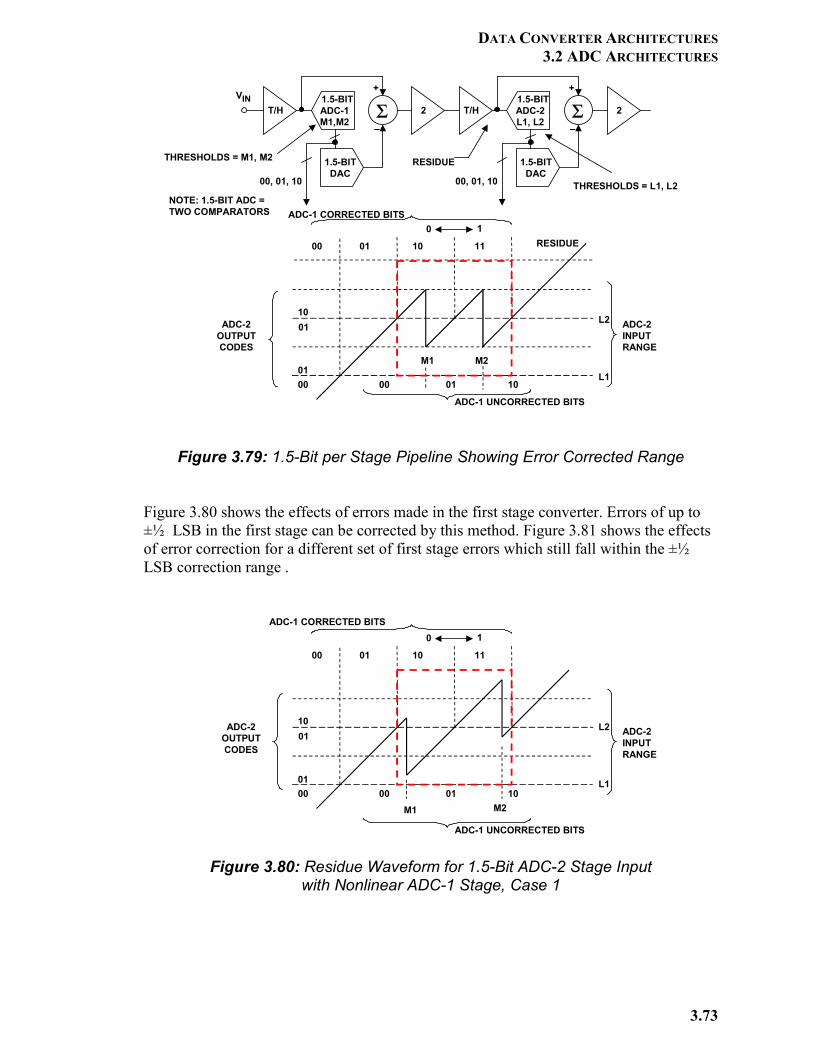
DATA CONVERTER ARCHITECTURES 3.2 ADC ARCHITECTURES
3.73
Figure 3.79: 1.5-Bit per Stage Pipeline Showing Error Corrected Range Figure 3.80 shows the effects of errors made in the first stage converter. Errors of up to ±½ LSB in the first stage can be corrected by this method. Figure 3.81 shows the effects of error correction for a different set of first stage errors which still fall within the ±½ LSB correction range .
Figure 3.80: Residue Waveform for 1.5-Bit ADC-2 Stage Input
with Nonlinear ADC-1 Stage, Case 1
T/H1.5-BITADC-1M1,M2
1.5-BITDAC
Σ+
–
2 T/HVIN 1.5-BIT
ADC-2L1, L2
1.5-BITDAC
Σ+
–
2
0001
0110
00 01 10
00 01 10 11
10
ADC-1 UNCORRECTED BITS
ADC-1 CORRECTED BITS
RESIDUE
RESIDUE
00, 01, 10
ADC-2INPUTRANGE
ADC-2OUTPUTCODES
00, 01, 10
NOTE: 1.5-BIT ADC =TWO COMPARATORS
L1
L2
M1 M2
THRESHOLDS = M1, M2
THRESHOLDS = L1, L2
0001
0110
00 01 10
00 01 10 11
10
ADC-1 UNCORRECTED BITS
ADC-1 CORRECTED BITS
ADC-2INPUTRANGE
L1
L2
M1 M2
ADC-2OUTPUTCODES
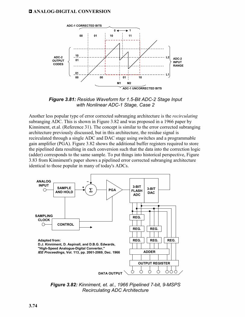
ANALOG-DIGITAL CONVERSION
3.74
Figure 3.81: Residue Waveform for 1.5-Bit ADC-2 Stage Input
with Nonlinear ADC-1 Stage, Case 2 Another less popular type of error corrected subranging architecture is the recirculating subranging ADC. This is shown in Figure 3.82 and was proposed in a 1966 paper by Kinniment, et.al. (Reference 31). The concept is similar to the error corrected subranging architecture previously discussed, but in this architecture, the residue signal is recirculated through a single ADC and DAC stage using switches and a programmable gain amplifier (PGA). Figure 3.82 shows the additional buffer registers required to store the pipelined data resulting in each conversion such that the data into the correction logic (adder) corresponds to the same sample. To put things into historical perspective, Figure 3.83 from Kinniment's paper shows a pipelined error corrected subranging architecture identical to those popular in many of today's ADCs.
Figure 3.82: Kinniment, et. al., 1966 Pipelined 7-bit, 9-MSPS
Recirculating ADC Architecture
0001
0110
00 01 10
00 01 10 11
10
M1 M2
ADC-2INPUTRANGE
L1
L2
ADC-1 CORRECTED BITS
ADC-2OUTPUTCODES
ADC-1 UNCORRECTED BITS
SAMPLEAND HOLD PGAΣ
3-BITFLASH
ADC
3-BITDAC
+
–
REG.
REG. REG.
REG. REG. REG.
ADDER
OUTPUT REGISTER
CONTROL
ANALOGINPUT
SAMPLINGCLOCK
Adapted from: D.J. Kinniment, D. Aspinall, and D.B.G. Edwards,"High-Speed Analogue-Digital Converter," IEE Proceedings, Vol. 113, pp. 2061-2069, Dec. 1966
DATA OUTPUT
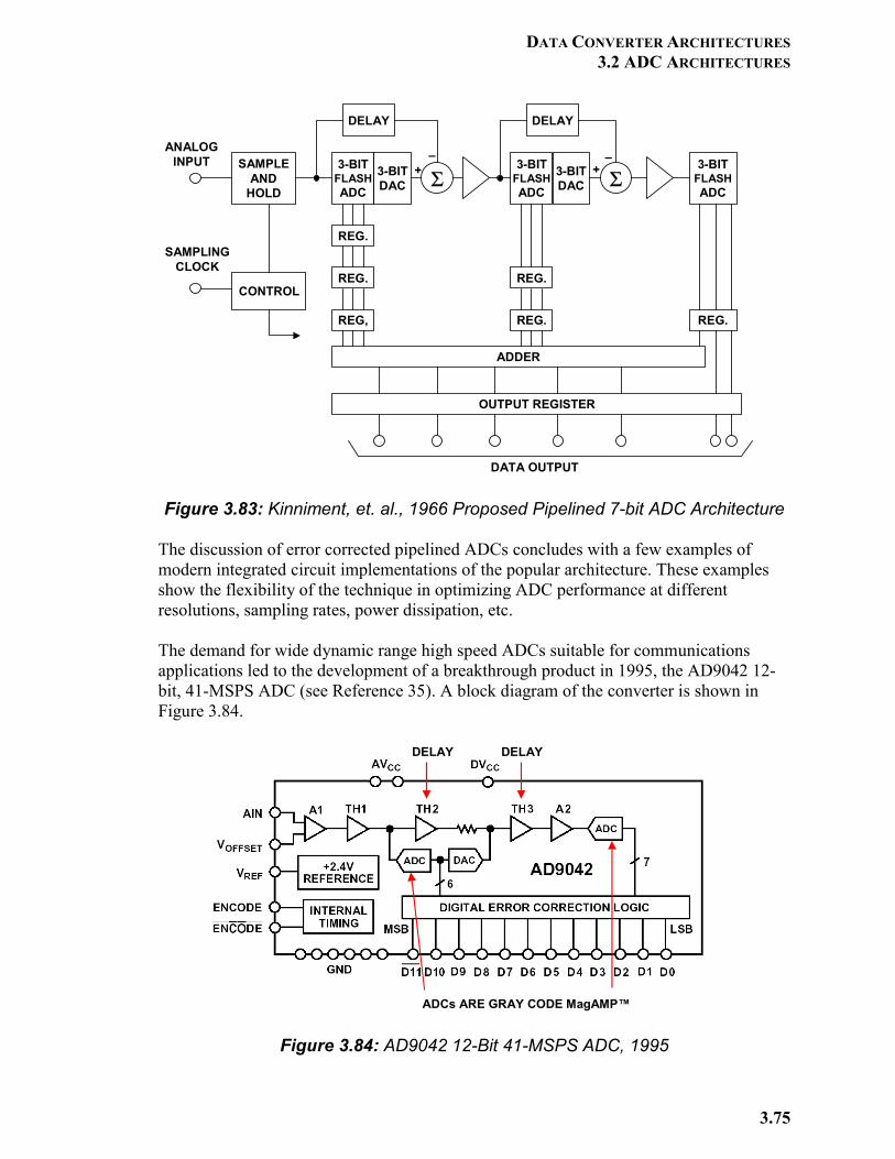
DATA CONVERTER ARCHITECTURES 3.2 ADC ARCHITECTURES
3.75
Figure 3.83: Kinniment, et. al., 1966 Proposed Pipelined 7-bit ADC Architecture
The discussion of error corrected pipelined ADCs concludes with a few examples of modern integrated circuit implementations of the popular architecture. These examples show the flexibility of the technique in optimizing ADC performance at different resolutions, sampling rates, power dissipation, etc. The demand for wide dynamic range high speed ADCs suitable for communications applications led to the development of a breakthrough product in 1995, the AD9042 12-bit, 41-MSPS ADC (see Reference 35). A block diagram of the converter is shown in Figure 3.84.
Figure 3.84: AD9042 12-Bit 41-MSPS ADC, 1995
+SAMPLEAND
HOLD
3-BITFLASHADC
3-BITDAC Σ
3-BITFLASHADC
3-BITDAC Σ
3-BITFLASHADC
DELAY DELAY
REG.
REG.
REG,
REG.
REG. REG.
ADDER
OUTPUT REGISTER
DATA OUTPUT
+– –
ANALOGINPUT
CONTROL
SAMPLINGCLOCK
ADCs ARE GRAY CODE MagAMP™
DELAY DELAY
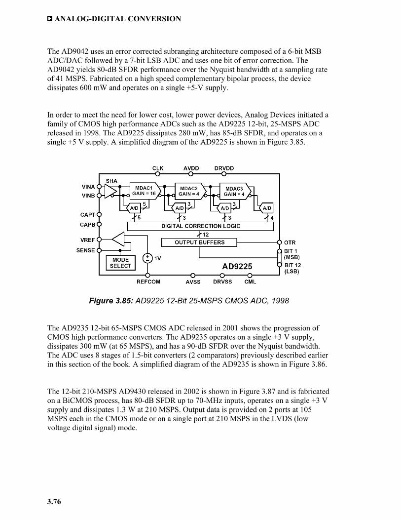
ANALOG-DIGITAL CONVERSION
3.76
The AD9042 uses an error corrected subranging architecture composed of a 6-bit MSB ADC/DAC followed by a 7-bit LSB ADC and uses one bit of error correction. The AD9042 yields 80-dB SFDR performance over the Nyquist bandwidth at a sampling rate of 41 MSPS. Fabricated on a high speed complementary bipolar process, the device dissipates 600 mW and operates on a single +5-V supply. In order to meet the need for lower cost, lower power devices, Analog Devices initiated a family of CMOS high performance ADCs such as the AD9225 12-bit, 25-MSPS ADC released in 1998. The AD9225 dissipates 280 mW, has 85-dB SFDR, and operates on a single +5 V supply. A simplified diagram of the AD9225 is shown in Figure 3.85.
Figure 3.85: AD9225 12-Bit 25-MSPS CMOS ADC, 1998
The AD9235 12-bit 65-MSPS CMOS ADC released in 2001 shows the progression of CMOS high performance converters. The AD9235 operates on a single +3 V supply, dissipates 300 mW (at 65 MSPS), and has a 90-dB SFDR over the Nyquist bandwidth. The ADC uses 8 stages of 1.5-bit converters (2 comparators) previously described earlier in this section of the book. A simplified diagram of the AD9235 is shown in Figure 3.86. The 12-bit 210-MSPS AD9430 released in 2002 is shown in Figure 3.87 and is fabricated on a BiCMOS process, has 80-dB SFDR up to 70-MHz inputs, operates on a single +3 V supply and dissipates 1.3 W at 210 MSPS. Output data is provided on 2 ports at 105 MSPS each in the CMOS mode or on a single port at 210 MSPS in the LVDS (low voltage digital signal) mode.
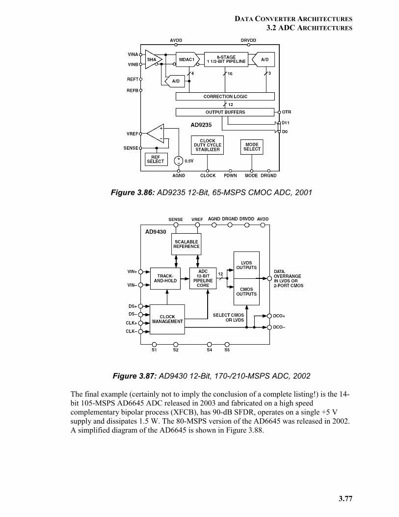
DATA CONVERTER ARCHITECTURES 3.2 ADC ARCHITECTURES
3.77
Figure 3.86: AD9235 12-Bit, 65-MSPS CMOC ADC, 2001
Figure 3.87: AD9430 12-Bit, 170-/210-MSPS ADC, 2002 The final example (certainly not to imply the conclusion of a complete listing!) is the 14-bit 105-MSPS AD6645 ADC released in 2003 and fabricated on a high speed complementary bipolar process (XFCB), has 90-dB SFDR, operates on a single +5 V supply and dissipates 1.5 W. The 80-MSPS version of the AD6645 was released in 2002. A simplified diagram of the AD6645 is shown in Figure 3.88.
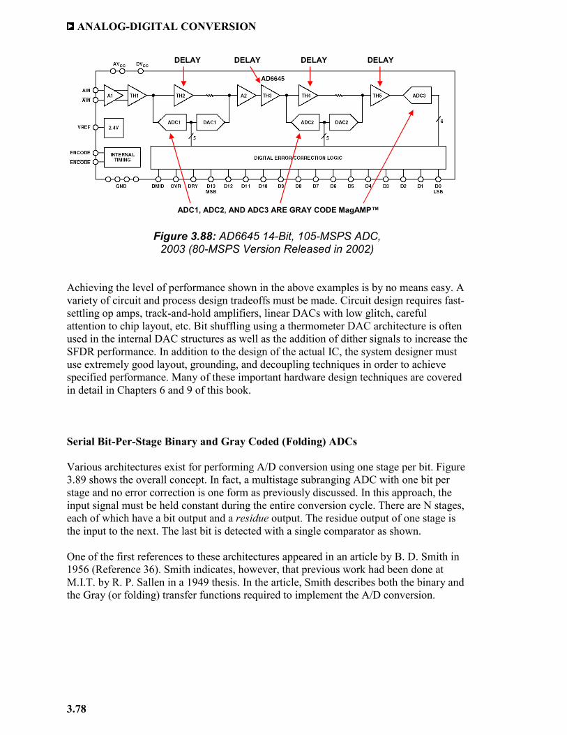
ANALOG-DIGITAL CONVERSION
3.78
Figure 3.88: AD6645 14-Bit, 105-MSPS ADC,
2003 (80-MSPS Version Released in 2002) Achieving the level of performance shown in the above examples is by no means easy. A variety of circuit and process design tradeoffs must be made. Circuit design requires fast-settling op amps, track-and-hold amplifiers, linear DACs with low glitch, careful attention to chip layout, etc. Bit shuffling using a thermometer DAC architecture is often used in the internal DAC structures as well as the addition of dither signals to increase the SFDR performance. In addition to the design of the actual IC, the system designer must use extremely good layout, grounding, and decoupling techniques in order to achieve specified performance. Many of these important hardware design techniques are covered in detail in Chapters 6 and 9 of this book. Serial Bit-Per-Stage Binary and Gray Coded (Folding) ADCs Various architectures exist for performing A/D conversion using one stage per bit. Figure 3.89 shows the overall concept. In fact, a multistage subranging ADC with one bit per stage and no error correction is one form as previously discussed. In this approach, the input signal must be held constant during the entire conversion cycle. There are N stages, each of which have a bit output and a residue output. The residue output of one stage is the input to the next. The last bit is detected with a single comparator as shown. One of the first references to these architectures appeared in an article by B. D. Smith in 1956 (Reference 36). Smith indicates, however, that previous work had been done at M.I.T. by R. P. Sallen in a 1949 thesis. In the article, Smith describes both the binary and the Gray (or folding) transfer functions required to implement the A/D conversion.
ADC1, ADC2, AND ADC3 ARE GRAY CODE MagAMP™
DELAY DELAYDELAY DELAY
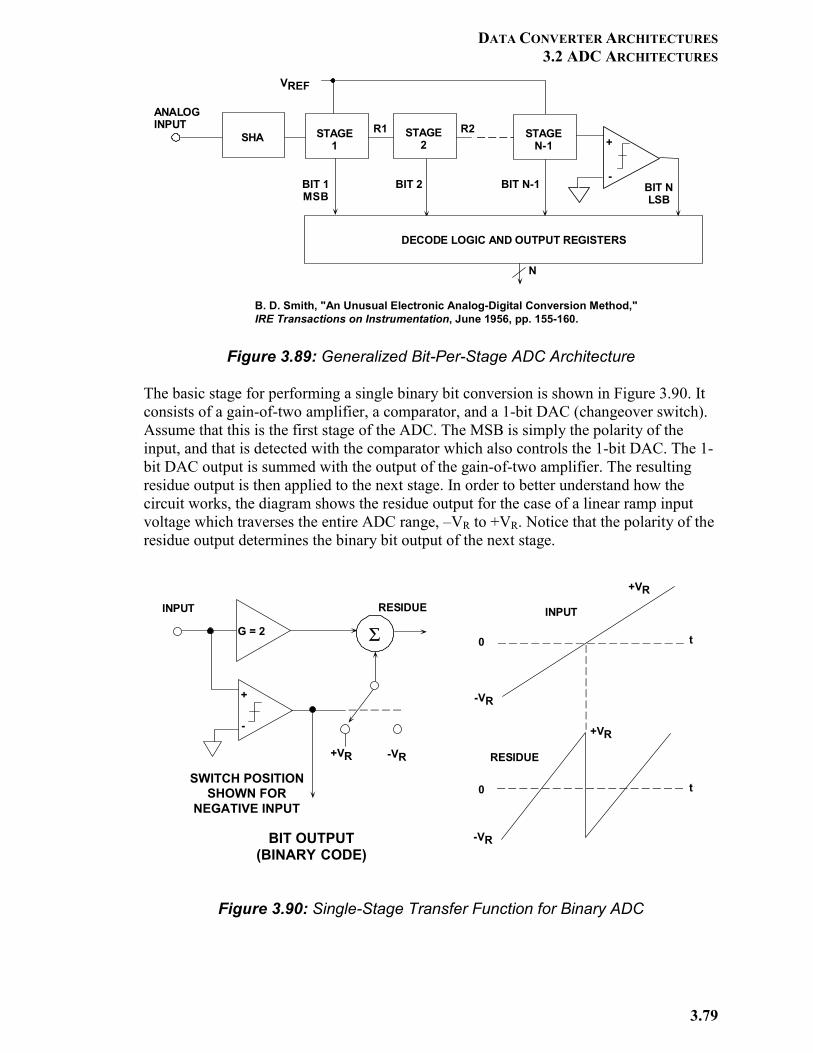
DATA CONVERTER ARCHITECTURES 3.2 ADC ARCHITECTURES
3.79
Figure 3.89: Generalized Bit-Per-Stage ADC Architecture
The basic stage for performing a single binary bit conversion is shown in Figure 3.90. It consists of a gain-of-two amplifier, a comparator, and a 1-bit DAC (changeover switch). Assume that this is the first stage of the ADC. The MSB is simply the polarity of the input, and that is detected with the comparator which also controls the 1-bit DAC. The 1-bit DAC output is summed with the output of the gain-of-two amplifier. The resulting residue output is then applied to the next stage. In order to better understand how the circuit works, the diagram shows the residue output for the case of a linear ramp input voltage which traverses the entire ADC range, –VR to +VR. Notice that the polarity of the residue output determines the binary bit output of the next stage.
Figure 3.90: Single-Stage Transfer Function for Binary ADC
ANALOGINPUT
SHA STAGE1
STAGE2
DECODE LOGIC AND OUTPUT REGISTERS
+
-BIT 1MSB
BIT 2
VREF
N
R1 R2 STAGEN-1
BIT N-1 BIT NLSB
B. D. Smith, "An Unusual Electronic Analog-Digital Conversion Method,"IRE Transactions on Instrumentation, June 1956, pp. 155-160.
INPUT INPUTRESIDUE
+VR
+VR
-VR
-VR
0
0
RESIDUE+VR -VR
G = 2
+
-
Σ
BIT OUTPUT(BINARY CODE)
SWITCH POSITIONSHOWN FOR
NEGATIVE INPUT
t
t
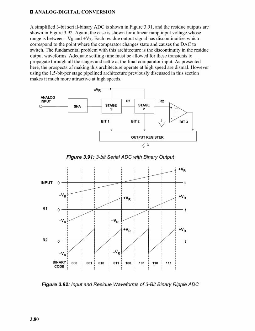
ANALOG-DIGITAL CONVERSION
3.80
A simplified 3-bit serial-binary ADC is shown in Figure 3.91, and the residue outputs are shown in Figure 3.92. Again, the case is shown for a linear ramp input voltage whose range is between –VR and +VR. Each residue output signal has discontinuities which correspond to the point where the comparator changes state and causes the DAC to switch. The fundamental problem with this architecture is the discontinuity in the residue output waveforms. Adequate settling time must be allowed for these transients to propagate through all the stages and settle at the final comparator input. As presented here, the prospects of making this architecture operate at high speed are dismal. However using the 1.5-bit-per stage pipelined architecture previously discussed in this section makes it much more attractive at high speeds.
Figure 3.91: 3-bit Serial ADC with Binary Output
Figure 3.92: Input and Residue Waveforms of 3-Bit Binary Ripple ADC
ANALOGINPUT
SHA STAGE1
STAGE2
OUTPUT REGISTER
+
-BIT 1 BIT 2 BIT 3
±VR
3
R1 R2
000 001 010 011 100 101 110 111
INPUT
R1
R2
–VR
–VR
–VR
+VR
+VR
+VR
0
0
0
t
t
t
BINARYCODE
+VR
–VR
+VR
–VR
DATA CONVERTER ARCHITECTURES 3.2 ADC ARCHITECTURES
3.81
Although the binary method is discussed in his paper, B. D. Smith also describes a much preferred bit-per-stage architecture based on absolute value amplifiers (magnitude amplifiers, or simply MagAMPs™). This scheme has often been referred to as serial-Gray (since the output coding is in Gray code), or folding converter because of the shape of the transfer function. Performing the conversion using a transfer function that produces an initial Gray code output has the advantage of minimizing discontinuities in the residue output waveforms and offers the potential of operating at much higher speeds than the binary approach. The basic folding stage is shown functionally in Figure 3.93 along with its transfer function. The input to the stage is assumed to be a linear ramp voltage whose range is between –VR and +VR. The comparator detects the polarity of the input signal and provides the Gray bit output for the stage. It also determines whether the overall stage gain is +2 or –2. The reference voltage VR is summed with the switch output to generate the residue signal which is applied to the next stage. The polarity of the residue signal determines the Gray bit for the next stage. The transfer function for the folding stage is also shown in Figure 3.93.
Figure 3.93: Folding Stage Functional Equivalent Circuit
A 3-bit MagAMP folding ADC is shown in Figure 3.94, and the corresponding residue waveforms in Figure 3.95. As in the case of the binary ripple ADC, the polarity of the residue output signal of a stage determines the value of the Gray bit for the next stage. The polarity of the input to the first stage determines the Gray MSB; the polarity of R1 output determines the Gray bit-2; and the polarity of R2 output determines the Gray bit-3. Notice that unlike the binary ripple ADC, there is no abrupt transition in any of the folding stage residue output waveforms. This makes operation at high speeds quite feasible.
INPUT
G = +2 INPUTRESIDUE
+VR
+VR
-VR
-VR
0
0
RESIDUE
VR
+
-
BIT OUTPUT(GRAY CODE)
G = -2
Σ
SWITCH POSITIONSHOWN FORNEGATIVE INPUT
t
t
ANALOG-DIGITAL CONVERSION
3.82
Figure 3.94: 3-bit Folding ADC Block Diagram
Figure 3.95: Input and Residue Waveforms for 3-Bit Folding ADC
The key to operating this architecture at high speeds is the folding stage. N. E. Chasek of Bell Telephone Labs describes a circuit for generating the folding transfer function using nested diode bridges in a patent filed in 1960 (Reference 37). This circuit made use of solid-state devices, but required different reference voltages for each stage (see Figure 3.96). Chasek's circuit also suffered from loss of headroom and gain when several stages were cascaded to form higher resolution converters as shown in Figure 3.97. What is really needed to make the folding ADC work at high resolutions is nearly ideal voltage or current rectification.
ANALOGINPUT
SHA MAGAMP1
MAGAMP2
GRAY-TO-BINARY CONVERTER
OUTPUT REGISTER
GRAY CODE REGISTER
+
-BIT 1 BIT 2 BIT 3
±VR
3
3
3
001 011 010 110 111 101000 100
INPUT
R1
R2
0
0
0
–VR
–VR
–VR
+VR
+VR
–VR
–VR
+VR +VR
–VR
t
t
t
GRAYCODE
DATA CONVERTER ARCHITECTURES 3.2 ADC ARCHITECTURES
3.83
Figure 3.96: 3-Bit Folding ADC Based on N. E. Chasek's Design
Figure 3.97: Single-Ended Waveforms in Chasek's Folding ADC
+
+ +
+
BALANCEDINPUT
BIAS
BIAS BIAS
BIAS
BIT 1 BIT 2 BIT 3
GRAY CODE OUTPUT
R1 R2
Adapted from: N. E. Chasek, "Pulse Code Modulation Encoder," U.S. Patent 3,035,258, Filed November 14, 1960, Issued May 15, 1962
001 011 010 110 111 101000 100
INPUT
R1
R2
0
0
0
–VR
–VR/2
+VR
+VR/2
–VR
t
t
t
GRAYCODE
–VR/2
–VR/4
+VR/4
–VR/4
ANALOG-DIGITAL CONVERSION
3.84
F. D. Waldhaur of Bell Telephone Labs remedied the problems of Chasek's nested diode bridge circuits in a classic patent filed in 1962 (Reference 38). Figure 3.98 shows Waldhaur's elegant implementation of the folding transfer function using solid state op amps with diodes in the feedback loop. The gain-of-two op amps allow the same reference voltages to be used for each stage and maintain the same signal level at each residue output with nearly ideal rectification.
Figure 3.98: F. D. Waldhaur's Classic Folding Stage using Rectifier Amplifiers
J. O. Edson and H. H. Henning describe the operation and performance of this type of ADC in greater detail in a 1965 Bell System Technical Journal article (Reference 39). An operational 9-bit, 6-MSPS ADC of this type was used in experimental studies on 224-Mbit/second PCM terminals. These terminals were supposed to handle data as well as voice signals. The voiceband objective was to digitize an entire 600-channel, 2.4-MHz FDM band, therefore requiring a minimum sampling rate of approximately 6 MSPS. It is interesting to note that the experimental terminal was also supposed to handle video as well, which required a higher sampling rate of approximately 12-MSPS. For this requirement, the latest (and final) generation Bell Labs' electron beam coder was needed to meet the ADC requirement, as the solid-state coder based on Waldhaur's patent did not have the necessary accuracy at the higher sampling rates. The first commercial ADC using Waldhaur's Gray code architecture was the 8-bit, 10-MSPS HS-810 from Computer Labs, Inc., in 1966 (see Chapter 1 of this book). The instrument used all discrete transistor circuits (no ICs) and was designed to be mounted in a 19" rack. The folding Gray code architecture was used in a few instrument and modular ADCs in the early 1970s, but was largely replaced by the error-corrected subranging architecture. With improvements in IC processes, there was renewed interest in the folding
–
+
–
+
R
R
2R
2R
2R
2R
R
R
R
R
IOFFSET
IOFFSET
BALANCEDINPUT BALANCED
OUTPUT
BITOUTPUT
i
i
i
i
3i 2i
2i
2i
2i
I
I
2i – I
2i – I3i
Extracted from: F. D. Waldhauer, "Analog-to-digital Converter,"U.S. Patent 3,187,325, Filed July 2, 1962, Issued June 1, 1965
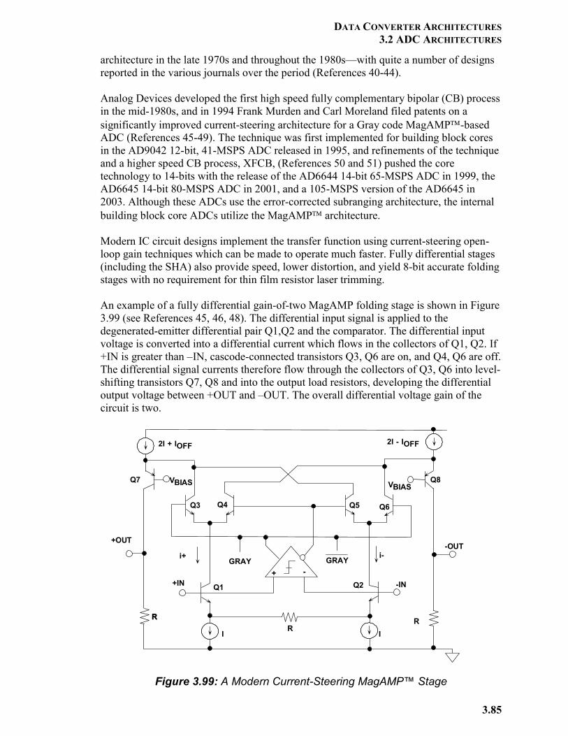
DATA CONVERTER ARCHITECTURES 3.2 ADC ARCHITECTURES
3.85
architecture in the late 1970s and throughout the 1980s—with quite a number of designs reported in the various journals over the period (References 40-44). Analog Devices developed the first high speed fully complementary bipolar (CB) process in the mid-1980s, and in 1994 Frank Murden and Carl Moreland filed patents on a significantly improved current-steering architecture for a Gray code MagAMP-based ADC (References 45-49). The technique was first implemented for building block cores in the AD9042 12-bit, 41-MSPS ADC released in 1995, and refinements of the technique and a higher speed CB process, XFCB, (References 50 and 51) pushed the core technology to 14-bits with the release of the AD6644 14-bit 65-MSPS ADC in 1999, the AD6645 14-bit 80-MSPS ADC in 2001, and a 105-MSPS version of the AD6645 in 2003. Although these ADCs use the error-corrected subranging architecture, the internal building block core ADCs utilize the MagAMP architecture. Modern IC circuit designs implement the transfer function using current-steering open-loop gain techniques which can be made to operate much faster. Fully differential stages (including the SHA) also provide speed, lower distortion, and yield 8-bit accurate folding stages with no requirement for thin film resistor laser trimming. An example of a fully differential gain-of-two MagAMP folding stage is shown in Figure 3.99 (see References 45, 46, 48). The differential input signal is applied to the degenerated-emitter differential pair Q1,Q2 and the comparator. The differential input voltage is converted into a differential current which flows in the collectors of Q1, Q2. If +IN is greater than –IN, cascode-connected transistors Q3, Q6 are on, and Q4, Q6 are off. The differential signal currents therefore flow through the collectors of Q3, Q6 into level-shifting transistors Q7, Q8 and into the output load resistors, developing the differential output voltage between +OUT and –OUT. The overall differential voltage gain of the circuit is two.
Figure 3.99: A Modern Current-Steering MagAMP™ Stage
VBIAS
Q4
Q7
+OUT
Q8
-OUT
R
-IN+IN
RR
II
Q6Q5Q3
Q1
GRAY GRAY
Q2
R
i+ i-
VBIAS
2I + IOFF 2I - IOFF
+ -
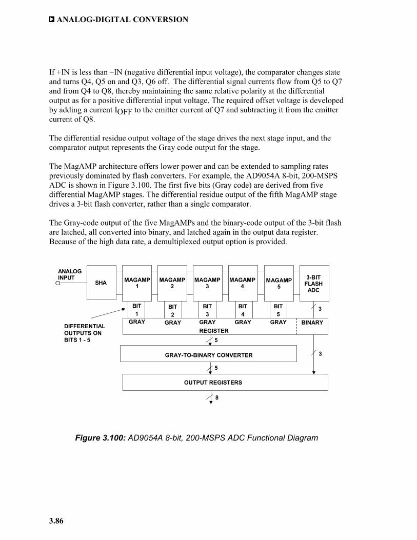
ANALOG-DIGITAL CONVERSION
3.86
If +IN is less than –IN (negative differential input voltage), the comparator changes state and turns Q4, Q5 on and Q3, Q6 off. The differential signal currents flow from Q5 to Q7 and from Q4 to Q8, thereby maintaining the same relative polarity at the differential output as for a positive differential input voltage. The required offset voltage is developed by adding a current IOFF to the emitter current of Q7 and subtracting it from the emitter current of Q8. The differential residue output voltage of the stage drives the next stage input, and the comparator output represents the Gray code output for the stage. The MagAMP architecture offers lower power and can be extended to sampling rates previously dominated by flash converters. For example, the AD9054A 8-bit, 200-MSPS ADC is shown in Figure 3.100. The first five bits (Gray code) are derived from five differential MagAMP stages. The differential residue output of the fifth MagAMP stage drives a 3-bit flash converter, rather than a single comparator. The Gray-code output of the five MagAMPs and the binary-code output of the 3-bit flash are latched, all converted into binary, and latched again in the output data register. Because of the high data rate, a demultiplexed output option is provided.
Figure 3.100: AD9054A 8-bit, 200-MSPS ADC Functional Diagram
5
5
8
ANALOGINPUT
SHA MAGAMP1
MAGAMP2
MAGAMP3
MAGAMP4
MAGAMP5
3-BITFLASH
ADC
BIT1
GRAY
BIT2
GRAY
BIT3
GRAY
BIT4
GRAY
BIT5
GRAY
3
REGISTER
GRAY-TO-BINARY CONVERTER
OUTPUT REGISTERS
BINARYDIFFERENTIALOUTPUTS ONBITS 1 - 5
3
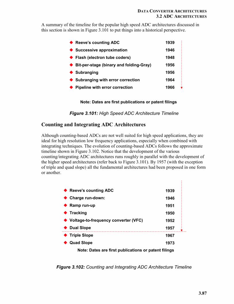
DATA CONVERTER ARCHITECTURES 3.2 ADC ARCHITECTURES
3.87
A summary of the timeline for the popular high speed ADC architectures discussed in this section is shown in Figure 3.101 to put things into a historical perspective.
Figure 3.101: High Speed ADC Architecture Timeline
Counting and Integrating ADC Architectures Although counting-based ADCs are not well suited for high speed applications, they are ideal for high resolution low frequency applications, especially when combined with integrating techniques. The evolution of counting-based ADCs follows the approximate timeline shown in Figure 3.102. Notice that the development of the various counting/integrating ADC architectures runs roughly in parallel with the development of the higher speed architectures (refer back to Figure 3.101). By 1957 (with the exception of triple and quad slope) all the fundamental architectures had been proposed in one form or another.
Figure 3.102: Counting and Integrating ADC Architecture Timeline
Reeve’s counting ADC
Successive approximation
Flash (electron tube coders)
Bit-per-stage (binary and folding-Gray)
Subranging
Subranging with error correction
Pipeline with error correction
1939
1946
1948
1956
1956
1964
1966
Note: Dates are first publications or patent filings
Reeve's counting ADC
Charge run-down:
Ramp run-up
Tracking
Voltage-to-frequency converter (VFC)
Dual Slope
Triple Slope
Quad Slope
1939
1946
1951
1950
1952
1957
1967
1973Note: Dates are first publications or patent filings
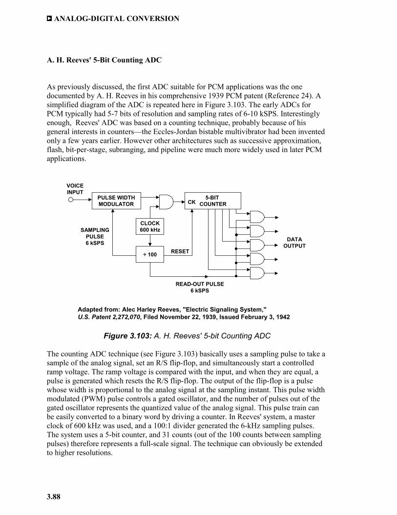
ANALOG-DIGITAL CONVERSION
3.88
A. H. Reeves' 5-Bit Counting ADC As previously discussed, the first ADC suitable for PCM applications was the one documented by A. H. Reeves in his comprehensive 1939 PCM patent (Reference 24). A simplified diagram of the ADC is repeated here in Figure 3.103. The early ADCs for PCM typically had 5-7 bits of resolution and sampling rates of 6-10 kSPS. Interestingly enough, Reeves' ADC was based on a counting technique, probably because of his general interests in counters—the Eccles-Jordan bistable multivibrator had been invented only a few years earlier. However other architectures such as successive approximation, flash, bit-per-stage, subranging, and pipeline were much more widely used in later PCM applications.
Figure 3.103: A. H. Reeves' 5-bit Counting ADC
The counting ADC technique (see Figure 3.103) basically uses a sampling pulse to take a sample of the analog signal, set an R/S flip-flop, and simultaneously start a controlled ramp voltage. The ramp voltage is compared with the input, and when they are equal, a pulse is generated which resets the R/S flip-flop. The output of the flip-flop is a pulse whose width is proportional to the analog signal at the sampling instant. This pulse width modulated (PWM) pulse controls a gated oscillator, and the number of pulses out of the gated oscillator represents the quantized value of the analog signal. This pulse train can be easily converted to a binary word by driving a counter. In Reeves' system, a master clock of 600 kHz was used, and a 100:1 divider generated the 6-kHz sampling pulses. The system uses a 5-bit counter, and 31 counts (out of the 100 counts between sampling pulses) therefore represents a full-scale signal. The technique can obviously be extended to higher resolutions.
PULSE WIDTHMODULATOR
CLOCK600 kHz
5-BIT COUNTER
÷ 100
SAMPLINGPULSE6 kSPS
READ-OUT PULSE6 kSPS
CK
RESET
VOICEINPUT
DATAOUTPUT
Adapted from: Alec Harley Reeves, "Electric Signaling System," U.S. Patent 2,272,070, Filed November 22, 1939, Issued February 3, 1942
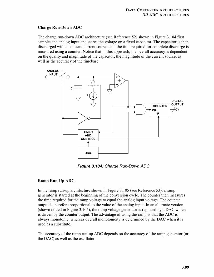
DATA CONVERTER ARCHITECTURES 3.2 ADC ARCHITECTURES
3.89
Charge Run-Down ADC The charge run-down ADC architecture (see Reference 52) shown in Figure 3.104 first samples the analog input and stores the voltage on a fixed capacitor. The capacitor is then discharged with a constant current source, and the time required for complete discharge is measured using a counter. Notice that in this approach, the overall accuracy is dependent on the quality and magnitude of the capacitor, the magnitude of the current source, as well as the accuracy of the timebase.
Figure 3.104: Charge Run-Down ADC
Ramp Run-Up ADC In the ramp run-up architecture shown in Figure 3.105 (see Reference 53), a ramp generator is started at the beginning of the conversion cycle. The counter then measures the time required for the ramp voltage to equal the analog input voltage. The counter output is therefore proportional to the value of the analog input. In an alternate version (shown dotted in Figure 3.105), the ramp voltage generator is replaced by a DAC which is driven by the counter output. The advantage of using the ramp is that the ADC is always monotonic, whereas overall monotonicity is determined by the DAC when it is used as a substitute. The accuracy of the ramp run-up ADC depends on the accuracy of the ramp generator (or the DAC) as well as the oscillator.
TIMERAND
CONTROL
OSC.
COUNTERCK
R
ANALOGINPUT
DIGITALOUTPUT
C
I
+
–
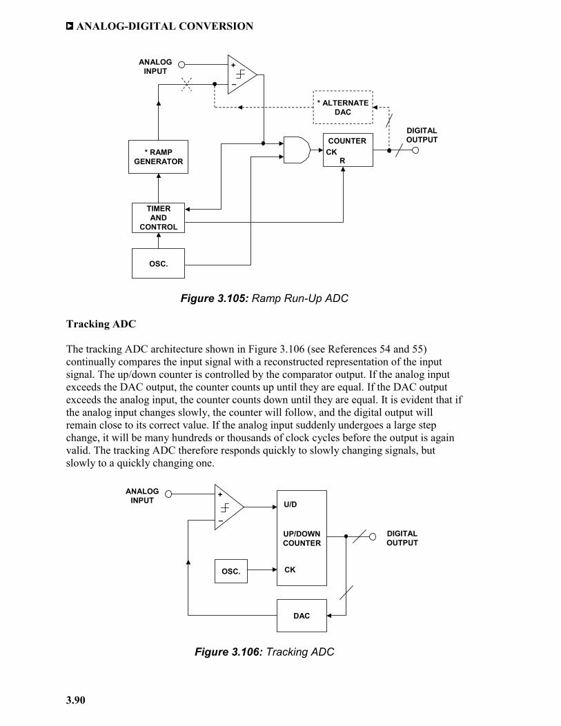
ANALOG-DIGITAL CONVERSION
3.90
Figure 3.105: Ramp Run-Up ADC
Tracking ADC The tracking ADC architecture shown in Figure 3.106 (see References 54 and 55) continually compares the input signal with a reconstructed representation of the input signal. The up/down counter is controlled by the comparator output. If the analog input exceeds the DAC output, the counter counts up until they are equal. If the DAC output exceeds the analog input, the counter counts down until they are equal. It is evident that if the analog input changes slowly, the counter will follow, and the digital output will remain close to its correct value. If the analog input suddenly undergoes a large step change, it will be many hundreds or thousands of clock cycles before the output is again valid. The tracking ADC therefore responds quickly to slowly changing signals, but slowly to a quickly changing one.
Figure 3.106: Tracking ADC
TIMERAND
CONTROL
OSC.
COUNTERCK
R
DIGITALOUTPUT
+
–
* ALTERNATEDAC
ANALOGINPUT
* RAMPGENERATOR
DIGITALOUTPUT
+
–
ANALOGINPUT
UP/DOWNCOUNTER
U/D
OSC. CK
DAC
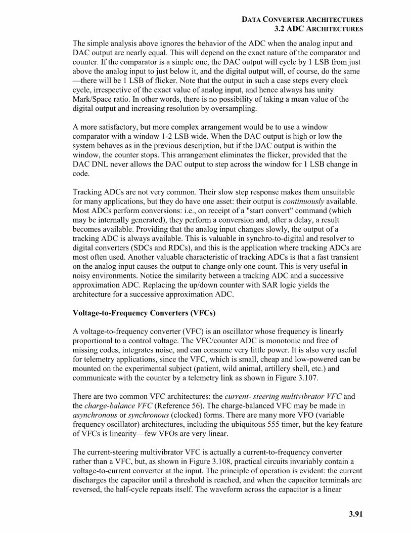
DATA CONVERTER ARCHITECTURES 3.2 ADC ARCHITECTURES
3.91
The simple analysis above ignores the behavior of the ADC when the analog input and DAC output are nearly equal. This will depend on the exact nature of the comparator and counter. If the comparator is a simple one, the DAC output will cycle by 1 LSB from just above the analog input to just below it, and the digital output will, of course, do the same —there will be 1 LSB of flicker. Note that the output in such a case steps every clock cycle, irrespective of the exact value of analog input, and hence always has unity Mark/Space ratio. In other words, there is no possibility of taking a mean value of the digital output and increasing resolution by oversampling. A more satisfactory, but more complex arrangement would be to use a window comparator with a window 1-2 LSB wide. When the DAC output is high or low the system behaves as in the previous description, but if the DAC output is within the window, the counter stops. This arrangement eliminates the flicker, provided that the DAC DNL never allows the DAC output to step across the window for 1 LSB change in code. Tracking ADCs are not very common. Their slow step response makes them unsuitable for many applications, but they do have one asset: their output is continuously available. Most ADCs perform conversions: i.e., on receipt of a "start convert" command (which may be internally generated), they perform a conversion and, after a delay, a result becomes available. Providing that the analog input changes slowly, the output of a tracking ADC is always available. This is valuable in synchro-to-digital and resolver to digital converters (SDCs and RDCs), and this is the application where tracking ADCs are most often used. Another valuable characteristic of tracking ADCs is that a fast transient on the analog input causes the output to change only one count. This is very useful in noisy environments. Notice the similarity between a tracking ADC and a successive approximation ADC. Replacing the up/down counter with SAR logic yields the architecture for a successive approximation ADC. Voltage-to-Frequency Converters (VFCs) A voltage-to-frequency converter (VFC) is an oscillator whose frequency is linearly proportional to a control voltage. The VFC/counter ADC is monotonic and free of missing codes, integrates noise, and can consume very little power. It is also very useful for telemetry applications, since the VFC, which is small, cheap and low-powered can be mounted on the experimental subject (patient, wild animal, artillery shell, etc.) and communicate with the counter by a telemetry link as shown in Figure 3.107. There are two common VFC architectures: the current- steering multivibrator VFC and the charge-balance VFC (Reference 56). The charge-balanced VFC may be made in asynchronous or synchronous (clocked) forms. There are many more VFO (variable frequency oscillator) architectures, including the ubiquitous 555 timer, but the key feature of VFCs is linearity—few VFOs are very linear. The current-steering multivibrator VFC is actually a current-to-frequency converter rather than a VFC, but, as shown in Figure 3.108, practical circuits invariably contain a voltage-to-current converter at the input. The principle of operation is evident: the current discharges the capacitor until a threshold is reached, and when the capacitor terminals are reversed, the half-cycle repeats itself. The waveform across the capacitor is a linear
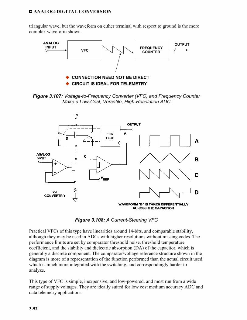
ANALOG-DIGITAL CONVERSION
3.92
triangular wave, but the waveform on either terminal with respect to ground is the more complex waveform shown.
Figure 3.107: Voltage-to-Frequency Converter (VFC) and Frequency Counter
Make a Low-Cost, Versatile, High-Resolution ADC
Figure 3.108: A Current-Steering VFC
Practical VFCs of this type have linearities around 14-bits, and comparable stability, although they may be used in ADCs with higher resolutions without missing codes. The performance limits are set by comparator threshold noise, threshold temperature coefficient, and the stability and dielectric absorption (DA) of the capacitor, which is generally a discrete component. The comparator/voltage reference structure shown in the diagram is more of a representation of the function performed than the actual circuit used, which is much more integrated with the switching, and correspondingly harder to analyze. This type of VFC is simple, inexpensive, and low-powered, and most run from a wide range of supply voltages. They are ideally suited for low cost medium accuracy ADC and data telemetry applications.
CONNECTION NEED NOT BE DIRECTCIRCUIT IS IDEAL FOR TELEMETRY
ANALOGINPUT
OUTPUTVFC FREQUENCY
COUNTER
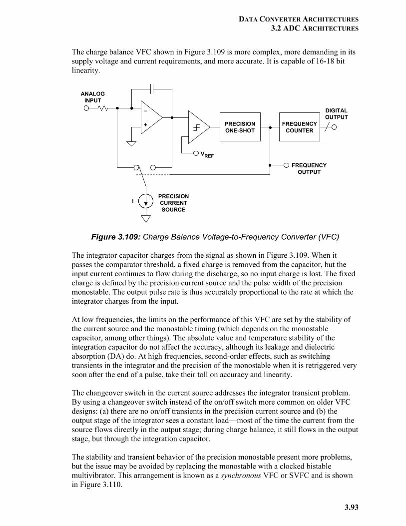
DATA CONVERTER ARCHITECTURES 3.2 ADC ARCHITECTURES
3.93
The charge balance VFC shown in Figure 3.109 is more complex, more demanding in its supply voltage and current requirements, and more accurate. It is capable of 16-18 bit linearity.
Figure 3.109: Charge Balance Voltage-to-Frequency Converter (VFC)
The integrator capacitor charges from the signal as shown in Figure 3.109. When it passes the comparator threshold, a fixed charge is removed from the capacitor, but the input current continues to flow during the discharge, so no input charge is lost. The fixed charge is defined by the precision current source and the pulse width of the precision monostable. The output pulse rate is thus accurately proportional to the rate at which the integrator charges from the input. At low frequencies, the limits on the performance of this VFC are set by the stability of the current source and the monostable timing (which depends on the monostable capacitor, among other things). The absolute value and temperature stability of the integration capacitor do not affect the accuracy, although its leakage and dielectric absorption (DA) do. At high frequencies, second-order effects, such as switching transients in the integrator and the precision of the monostable when it is retriggered very soon after the end of a pulse, take their toll on accuracy and linearity. The changeover switch in the current source addresses the integrator transient problem. By using a changeover switch instead of the on/off switch more common on older VFC designs: (a) there are no on/off transients in the precision current source and (b) the output stage of the integrator sees a constant load—most of the time the current from the source flows directly in the output stage; during charge balance, it still flows in the output stage, but through the integration capacitor. The stability and transient behavior of the precision monostable present more problems, but the issue may be avoided by replacing the monostable with a clocked bistable multivibrator. This arrangement is known as a synchronous VFC or SVFC and is shown in Figure 3.110.
+
–
PRECISIONONE-SHOT
I
FREQUENCYCOUNTER
VREF
PRECISIONCURRENTSOURCE
ANALOGINPUT
FREQUENCYOUTPUT
DIGITALOUTPUT
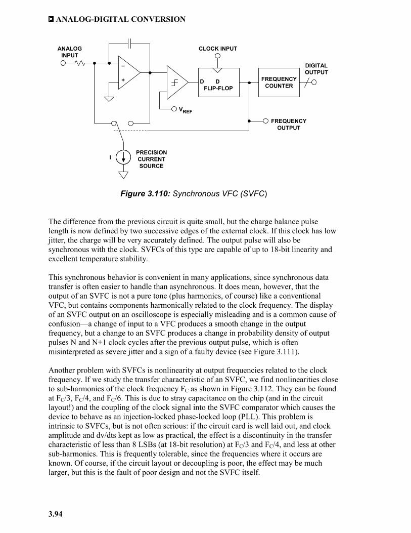
ANALOG-DIGITAL CONVERSION
3.94
Figure 3.110: Synchronous VFC (SVFC)
The difference from the previous circuit is quite small, but the charge balance pulse length is now defined by two successive edges of the external clock. If this clock has low jitter, the charge will be very accurately defined. The output pulse will also be synchronous with the clock. SVFCs of this type are capable of up to 18-bit linearity and excellent temperature stability. This synchronous behavior is convenient in many applications, since synchronous data transfer is often easier to handle than asynchronous. It does mean, however, that the output of an SVFC is not a pure tone (plus harmonics, of course) like a conventional VFC, but contains components harmonically related to the clock frequency. The display of an SVFC output on an oscilloscope is especially misleading and is a common cause of confusion—a change of input to a VFC produces a smooth change in the output frequency, but a change to an SVFC produces a change in probability density of output pulses N and N+1 clock cycles after the previous output pulse, which is often misinterpreted as severe jitter and a sign of a faulty device (see Figure 3.111). Another problem with SVFCs is nonlinearity at output frequencies related to the clock frequency. If we study the transfer characteristic of an SVFC, we find nonlinearities close to sub-harmonics of the clock frequency FC as shown in Figure 3.112. They can be found at FC/3, FC/4, and FC/6. This is due to stray capacitance on the chip (and in the circuit layout!) and the coupling of the clock signal into the SVFC comparator which causes the device to behave as an injection-locked phase-locked loop (PLL). This problem is intrinsic to SVFCs, but is not often serious: if the circuit card is well laid out, and clock amplitude and dv/dts kept as low as practical, the effect is a discontinuity in the transfer characteristic of less than 8 LSBs (at 18-bit resolution) at FC/3 and FC/4, and less at other sub-harmonics. This is frequently tolerable, since the frequencies where it occurs are known. Of course, if the circuit layout or decoupling is poor, the effect may be much larger, but this is the fault of poor design and not the SVFC itself.
+
–
I
FREQUENCYCOUNTER
VREF
PRECISIONCURRENTSOURCE
ANALOGINPUT
FREQUENCYOUTPUT
DIGITALOUTPUT
D FLIP-FLOP
D
CLOCK INPUT
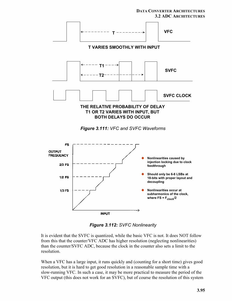
DATA CONVERTER ARCHITECTURES 3.2 ADC ARCHITECTURES
3.95
Figure 3.111: VFC and SVFC Waveforms
Figure 3.112: SVFC Nonlinearity
It is evident that the SVFC is quantized, while the basic VFC is not. It does NOT follow from this that the counter/VFC ADC has higher resolution (neglecting nonlinearities) than the counter/SVFC ADC, because the clock in the counter also sets a limit to the resolution. When a VFC has a large input, it runs quickly and (counting for a short time) gives good resolution, but it is hard to get good resolution in a reasonable sample time with a slow-running VFC. In such a case, it may be more practical to measure the period of the VFC output (this does not work for an SVFC), but of course the resolution of this system
VFC
SVFC
SVFC CLOCK
T VARIES SMOOTHLY WITH INPUT
T
T1
T2
THE RELATIVE PROBABILITY OF DELAYT1 OR T2 VARIES WITH INPUT, BUT
BOTH DELAYS DO OCCUR
Nonlinearities caused by injection locking due to clock feedthrough
Should only be 6-8 LSBs at 18-bits with proper layout and decoupling
Nonlinearities occur atsubharmonics of the clock, where FS = Fclock/2
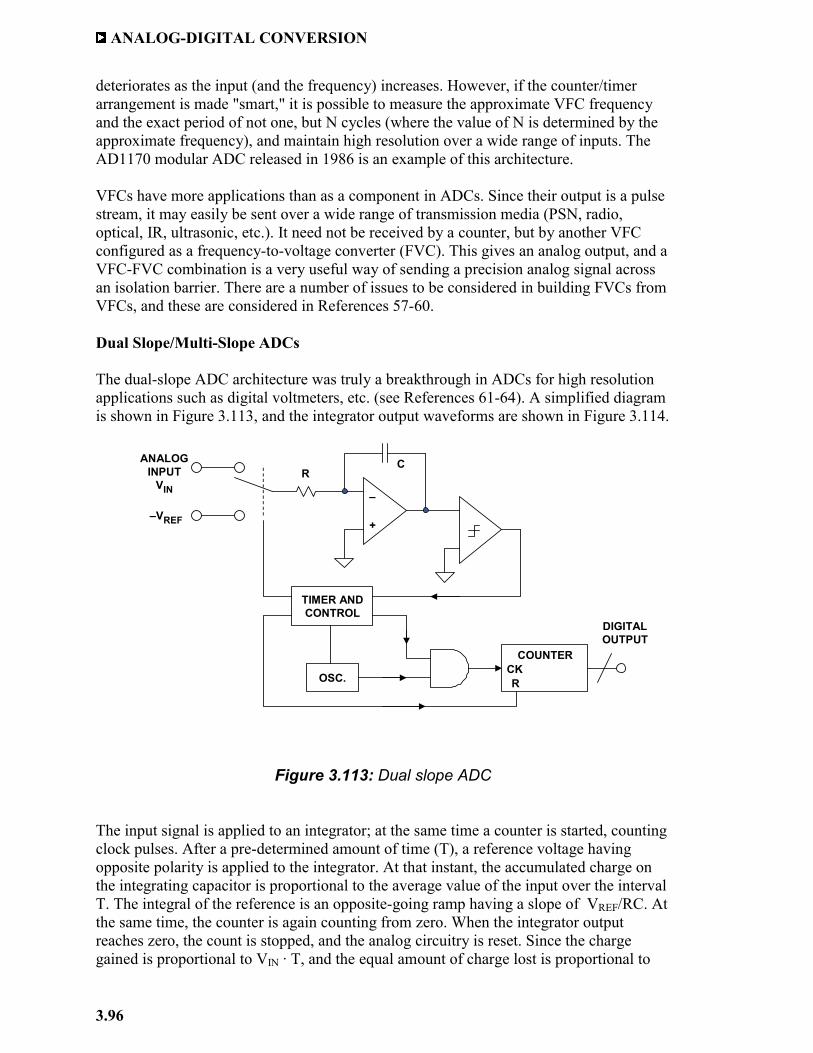
ANALOG-DIGITAL CONVERSION
3.96
deteriorates as the input (and the frequency) increases. However, if the counter/timer arrangement is made "smart," it is possible to measure the approximate VFC frequency and the exact period of not one, but N cycles (where the value of N is determined by the approximate frequency), and maintain high resolution over a wide range of inputs. The AD1170 modular ADC released in 1986 is an example of this architecture. VFCs have more applications than as a component in ADCs. Since their output is a pulse stream, it may easily be sent over a wide range of transmission media (PSN, radio, optical, IR, ultrasonic, etc.). It need not be received by a counter, but by another VFC configured as a frequency-to-voltage converter (FVC). This gives an analog output, and a VFC-FVC combination is a very useful way of sending a precision analog signal across an isolation barrier. There are a number of issues to be considered in building FVCs from VFCs, and these are considered in References 57-60. Dual Slope/Multi-Slope ADCs The dual-slope ADC architecture was truly a breakthrough in ADCs for high resolution applications such as digital voltmeters, etc. (see References 61-64). A simplified diagram is shown in Figure 3.113, and the integrator output waveforms are shown in Figure 3.114.
Figure 3.113: Dual slope ADC
The input signal is applied to an integrator; at the same time a counter is started, counting clock pulses. After a pre-determined amount of time (T), a reference voltage having opposite polarity is applied to the integrator. At that instant, the accumulated charge on the integrating capacitor is proportional to the average value of the input over the interval T. The integral of the reference is an opposite-going ramp having a slope of VREF/RC. At the same time, the counter is again counting from zero. When the integrator output reaches zero, the count is stopped, and the analog circuitry is reset. Since the charge gained is proportional to VIN · T, and the equal amount of charge lost is proportional to
+
–
ANALOGINPUT
VIN
–VREF
OSC.
TIMER ANDCONTROL
CKCOUNTER
R
DIGITALOUTPUT
RC
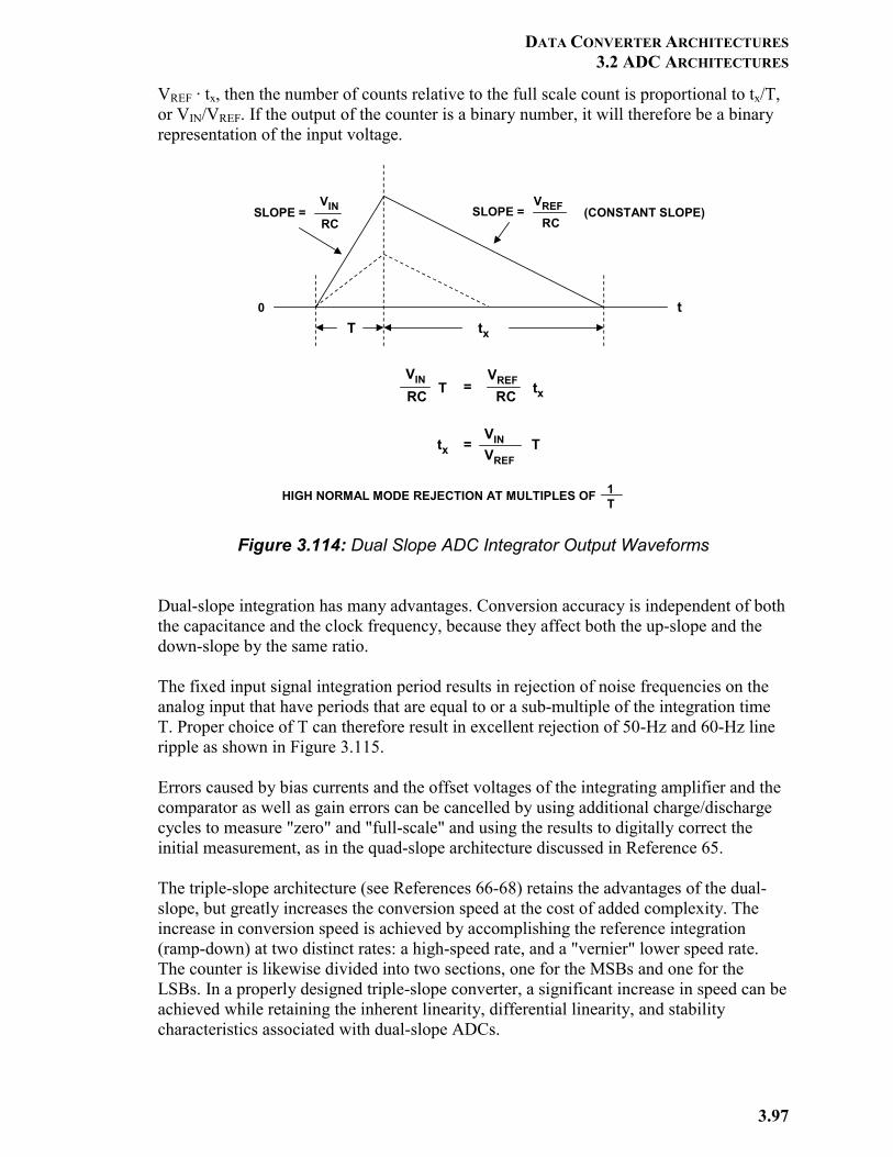
DATA CONVERTER ARCHITECTURES 3.2 ADC ARCHITECTURES
3.97
VREF · tx, then the number of counts relative to the full scale count is proportional to tx/T, or VIN/VREF. If the output of the counter is a binary number, it will therefore be a binary representation of the input voltage.
Figure 3.114: Dual Slope ADC Integrator Output Waveforms
Dual-slope integration has many advantages. Conversion accuracy is independent of both the capacitance and the clock frequency, because they affect both the up-slope and the down-slope by the same ratio. The fixed input signal integration period results in rejection of noise frequencies on the analog input that have periods that are equal to or a sub-multiple of the integration time T. Proper choice of T can therefore result in excellent rejection of 50-Hz and 60-Hz line ripple as shown in Figure 3.115. Errors caused by bias currents and the offset voltages of the integrating amplifier and the comparator as well as gain errors can be cancelled by using additional charge/discharge cycles to measure "zero" and "full-scale" and using the results to digitally correct the initial measurement, as in the quad-slope architecture discussed in Reference 65. The triple-slope architecture (see References 66-68) retains the advantages of the dual-slope, but greatly increases the conversion speed at the cost of added complexity. The increase in conversion speed is achieved by accomplishing the reference integration (ramp-down) at two distinct rates: a high-speed rate, and a "vernier" lower speed rate. The counter is likewise divided into two sections, one for the MSBs and one for the LSBs. In a properly designed triple-slope converter, a significant increase in speed can be achieved while retaining the inherent linearity, differential linearity, and stability characteristics associated with dual-slope ADCs.
0T tx
SLOPE = VIN
RCSLOPE =
VREFRC
VIN
RC TVREF
RC= tx
tx =VINVREF
T
(CONSTANT SLOPE)
t
HIGH NORMAL MODE REJECTION AT MULTIPLES OF 1T
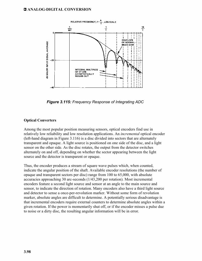
ANALOG-DIGITAL CONVERSION
3.98
Figure 3.115: Frequency Response of Integrating ADC Optical Converters Among the most popular position measuring sensors, optical encoders find use in relatively low reliability and low resolution applications. An incremental optical encoder (left-hand diagram in Figure 3.116) is a disc divided into sectors that are alternately transparent and opaque. A light source is positioned on one side of the disc, and a light sensor on the other side. As the disc rotates, the output from the detector switches alternately on and off, depending on whether the sector appearing between the light source and the detector is transparent or opaque. Thus, the encoder produces a stream of square wave pulses which, when counted, indicate the angular position of the shaft. Available encoder resolutions (the number of opaque and transparent sectors per disc) range from 100 to 65,000, with absolute accuracies approaching 30 arc-seconds (1/43,200 per rotation). Most incremental encoders feature a second light source and sensor at an angle to the main source and sensor, to indicate the direction of rotation. Many encoders also have a third light source and detector to sense a once-per-revolution marker. Without some form of revolution marker, absolute angles are difficult to determine. A potentially serious disadvantage is that incremental encoders require external counters to determine absolute angles within a given rotation. If the power is momentarily shut off, or if the encoder misses a pulse due to noise or a dirty disc, the resulting angular information will be in error.
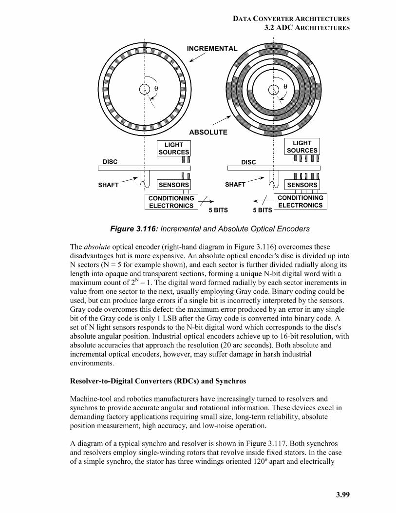
DATA CONVERTER ARCHITECTURES 3.2 ADC ARCHITECTURES
3.99
Figure 3.116: Incremental and Absolute Optical Encoders
The absolute optical encoder (right-hand diagram in Figure 3.116) overcomes these disadvantages but is more expensive. An absolute optical encoder's disc is divided up into N sectors (N = 5 for example shown), and each sector is further divided radially along its length into opaque and transparent sections, forming a unique N-bit digital word with a maximum count of 2N – 1. The digital word formed radially by each sector increments in value from one sector to the next, usually employing Gray code. Binary coding could be used, but can produce large errors if a single bit is incorrectly interpreted by the sensors. Gray code overcomes this defect: the maximum error produced by an error in any single bit of the Gray code is only 1 LSB after the Gray code is converted into binary code. A set of N light sensors responds to the N-bit digital word which corresponds to the disc's absolute angular position. Industrial optical encoders achieve up to 16-bit resolution, with absolute accuracies that approach the resolution (20 arc seconds). Both absolute and incremental optical encoders, however, may suffer damage in harsh industrial environments. Resolver-to-Digital Converters (RDCs) and Synchros Machine-tool and robotics manufacturers have increasingly turned to resolvers and synchros to provide accurate angular and rotational information. These devices excel in demanding factory applications requiring small size, long-term reliability, absolute position measurement, high accuracy, and low-noise operation. A diagram of a typical synchro and resolver is shown in Figure 3.117. Both sycnchros and resolvers employ single-winding rotors that revolve inside fixed stators. In the case of a simple synchro, the stator has three windings oriented 120º apart and electrically
LIGHTSOURCES
SENSORS
CONDITIONINGELECTRONICS
SHAFT
DISC
LIGHTSOURCES
SENSORS
CONDITIONINGELECTRONICS
DISC
5 BITS
SHAFT
INCREMENTAL
ABSOLUTE
5 BITS
θ θ
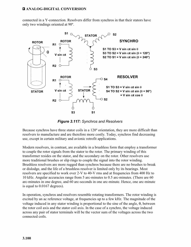
ANALOG-DIGITAL CONVERSION
3.100
connected in a Y-connection. Resolvers differ from synchros in that their stators have only two windings oriented at 90º.
Figure 3.117: Synchros and Resolvers
Because synchros have three stator coils in a 120º orientation, they are more difficult than resolvers to manufacture and are therefore more costly. Today, synchros find decreasing use, except in certain military and avionic retrofit applications. Modern resolvers, in contrast, are available in a brushless form that employ a transformer to couple the rotor signals from the stator to the rotor. The primary winding of this transformer resides on the stator, and the secondary on the rotor. Other resolvers use more traditional brushes or slip rings to couple the signal into the rotor winding. Brushless resolvers are more rugged than synchros because there are no brushes to break or dislodge, and the life of a brushless resolver is limited only by its bearings. Most resolvers are specified to work over 2-V to 40-V rms and at frequencies from 400 Hz to 10 kHz. Angular accuracies range from 5 arc-minutes to 0.5 arc-minutes. (There are 60 arc-minutes in one degree, and 60 arc-seconds in one arc-minute. Hence, one arc-minute is equal to 0.0167 degrees). In operation, synchros and resolvers resemble rotating transformers. The rotor winding is excited by an ac reference voltage, at frequencies up to a few kHz. The magnitude of the voltage induced in any stator winding is proportional to the sine of the angle, θ, between the rotor coil axis and the stator coil axis. In the case of a synchro, the voltage induced across any pair of stator terminals will be the vector sum of the voltages across the two connected coils.
R1
R2
S1 S2
S3
R1
R2
S1
S2
S3
S4
S1 TO S3 = V sin ωt sin θS3 TO S2 = V sin ωt sin (θ + 120°)S2 TO S1 = V sin ωt sin (θ + 240°)
S1 TO S3 = V sin ωt sin θS4 TO S2 = V sin ωt sin (θ + 90°)
= V sin ωt cos θ
ROTOR
ROTOR
STATOR
STATOR
ROTOR
STATOR
SYNCHRO
RESOLVER
V sin ωt
V sin ωt
θ
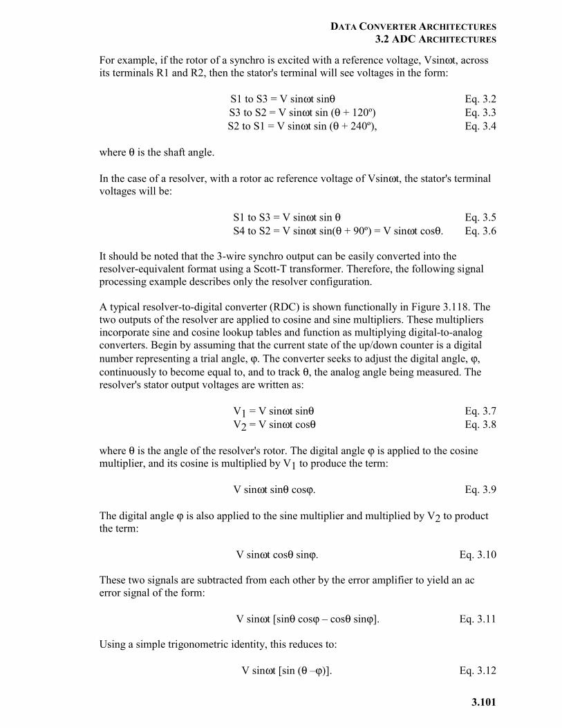
DATA CONVERTER ARCHITECTURES 3.2 ADC ARCHITECTURES
3.101
For example, if the rotor of a synchro is excited with a reference voltage, Vsinωt, across its terminals R1 and R2, then the stator's terminal will see voltages in the form:
S1 to S3 = V sinωt sinθ Eq. 3.2 S3 to S2 = V sinωt sin (θ + 120º) Eq. 3.3 S2 to S1 = V sinωt sin (θ + 240º), Eq. 3.4
where θ is the shaft angle. In the case of a resolver, with a rotor ac reference voltage of Vsinωt, the stator's terminal voltages will be:
S1 to S3 = V sinωt sin θ Eq. 3.5 S4 to S2 = V sinωt sin(θ + 90º) = V sinωt cosθ. Eq. 3.6
It should be noted that the 3-wire synchro output can be easily converted into the resolver-equivalent format using a Scott-T transformer. Therefore, the following signal processing example describes only the resolver configuration. A typical resolver-to-digital converter (RDC) is shown functionally in Figure 3.118. The two outputs of the resolver are applied to cosine and sine multipliers. These multipliers incorporate sine and cosine lookup tables and function as multiplying digital-to-analog converters. Begin by assuming that the current state of the up/down counter is a digital number representing a trial angle, ϕ. The converter seeks to adjust the digital angle, ϕ, continuously to become equal to, and to track θ, the analog angle being measured. The resolver's stator output voltages are written as:
V1 = V sinωt sinθ Eq. 3.7 V2 = V sinωt cosθ Eq. 3.8
where θ is the angle of the resolver's rotor. The digital angle ϕ is applied to the cosine multiplier, and its cosine is multiplied by V1 to produce the term:
V sinωt sinθ cosϕ. Eq. 3.9 The digital angle ϕ is also applied to the sine multiplier and multiplied by V2 to product the term: V sinωt cosθ sinϕ. Eq. 3.10
These two signals are subtracted from each other by the error amplifier to yield an ac error signal of the form: V sinωt [sinθ cosϕ – cosθ sinϕ]. Eq. 3.11
Using a simple trigonometric identity, this reduces to:
V sinωt [sin (θ –ϕ)]. Eq. 3.12
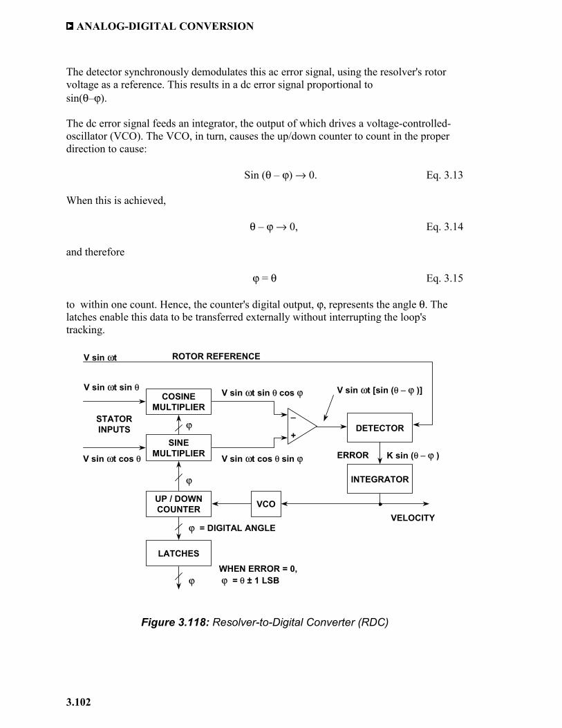
ANALOG-DIGITAL CONVERSION
3.102
The detector synchronously demodulates this ac error signal, using the resolver's rotor voltage as a reference. This results in a dc error signal proportional to sin(θ–ϕ). The dc error signal feeds an integrator, the output of which drives a voltage-controlled-oscillator (VCO). The VCO, in turn, causes the up/down counter to count in the proper direction to cause:
Sin (θ – ϕ) → 0. Eq. 3.13 When this is achieved,
θ – ϕ → 0, Eq. 3.14 and therefore
ϕ = θ Eq. 3.15 to within one count. Hence, the counter's digital output, ϕ, represents the angle θ. The latches enable this data to be transferred externally without interrupting the loop's tracking.
Figure 3.118: Resolver-to-Digital Converter (RDC)
COSINEMULTIPLIER
SINEMULTIPLIER
DETECTOR
INTEGRATOR
UP / DOWNCOUNTER VCO
V sin ωt sin θ
V sin ωt cos θ
V sin ωt sin θ cos ϕ
V sin ωt cos θ sin ϕ
_
+
V sin ωt [sin (θ – ϕ )]
ERROR
V sin ωt ROTOR REFERENCE
STATORINPUTS
LATCHES
K sin (θ – ϕ )
ϕ
ϕ = DIGITAL ANGLE
ϕ
VELOCITY
WHEN ERROR = 0,ϕ = θ ± 1 LSB
ϕ
DATA CONVERTER ARCHITECTURES 3.2 ADC ARCHITECTURES
3.103
This circuit is equivalent to a so-called type-2 servo loop, because it has, in effect, two integrators. One is the counter, which accumulates pulses; the other is the integrator at the output of the detector. In a type-2 servo loop with a constant rotational velocity input, the output digital word continuously follows, or tracks the input, without needing externally derived convert commands, and with no steady state phase lag between the digital output word and actual shaft angle. An error signal appears only during periods of acceleration or deceleration. As an added bonus, the tracking RDC provides an analog dc output voltage directly proportional to the shaft's rotational velocity. This is a useful feature if velocity is to be measured or used as a stabilization term in a servo system, and it makes additional tachometers unnecessary. Since the operation of an RDC depends only on the ratio between input signal amplitudes, attenuation in the lines connecting them to resolvers doesn't substantially affect performance. For similar reasons, these converters are not greatly susceptible to waveform distortion. In fact, they can operate with as much as 10% harmonic distortion on the input signals; some applications actually use square-wave references with little additional error. Tracking ADCs are therefore ideally suited to RDCs. While other ADC architectures, such as successive approximation, could be used, the tracking converter is the most accurate and efficient for this application. Because the tracking converter doubly integrates its error signal, the device offers a high degree of noise immunity (12-dB-per-octave rolloff). The net area under any given noise spike produces an error. However, typical inductively coupled noise spikes have equal positive and negative going waveforms. When integrated, this results in a zero net error signal. The resulting noise immunity, combined with the converter's insensitivity to voltage drops, lets the user locate the converter at a considerable distance from the resolver. Noise rejection is further enhanced by the detector's rejection of any signal not at the reference frequency, such as wideband noise. The AD2S90 is one of a number of integrated RDCs offered by Analog Devices. The general architecture is similar to that of Figure 3.118. Further details on synchro and resolver-to-digital converters can be found in References 69 and 70.
ANALOG-DIGITAL CONVERSION
3.104
REFERENCES: 3.2 ADC ARCHITECTURES 1. Reza Moghimi, "Amplifiers as Comparators," Ask the Applications Engineer 31, Analog Dialogue,
Vol. 37-04, Analog Devices, April 2003, http://www.analog.com. 2. James N. Giles, "High Speed Transistor Difference Amplifier," U.S. Patent 3,843,934, filed January
31 1973, issued October 22, 1974. (describes one of the first high-speed ECL comparators, the AM685).
3. Christopher W. Mangelsdorf, A 400-MHz Input Flash Converter with Error Correction, IEEE
Journal of Solid-State Circuits, Vol. 25, No. 1, February 1990, pp. 184-191. (a discussion of the AD770, an 8-bit 200 MSPS flash ADC. The paper describes the comparator metastable state problem and how to optimize the ADC design to minimize its effects).
4. Charles E. Woodward, A Monolithic Voltage-Comparator Array for A/D Converters, IEEE Journal of
Solid State Circuits, Vol. SC-10, No. 6, December 1975, pp. 392-399. (an early paper on a 3-bit flash converter optimized to minimize metastable state errors).
5. Paul M. Rainey, "Facimile Telegraph System," U.S. Patent 1,608,527, filed July 20, 1921, issued
November 30, 1926. (although A. H. Reeves is generally credited with the invention of PCM, this patent discloses an electro-mechanical PCM system complete with A/D and D/A converters. The 5-bit electro-mechanical ADC described is probably the first documented flash converter. The patent was largely ignored and forgotten until many years after the various Reeves' patents were issued in 1939-1942).
6. R. W. Sears, "Electron Beam Deflection Tube for Pulse Code Modulation," Bell System Technical
Journal, Vol. 27, pp. 44-57, Jan. 1948. (describes an electon-beam deflection tube 7-bit, 100-kSPS flash converter for early experimental PCM work).
7. Frank Gray, "Pulse Code Communication," U.S. Patent 2,632,058, filed November 13, 1947, issued
March 17, 1953. (detailed patent on the Gray code and its application to electron beam coders). 8. J. O. Edson and H. H. Henning, "Broadband Codecs for an Experimental 224Mb/s PCM Terminal,"
Bell System Technical Journal, Vol. 44, pp. 1887-1940, Nov. 1965. (summarizes experiments on ADCs based on the electron tube coder as well as a bit-per-stage Gray code 9-bit solid state ADC. The electron beam coder was 9-bits at 12 MSPS, and represented the fastest of its type at the time).
9. R. Staffin and R. D. Lohman, "Signal Amplitude Quantizer," U.S. Patent 2,869,079, filed December
19, 1956, issued January 13, 1959. (describes flash and subranging conversion using tubes and transistors).
10. Goto, et. al., "Esaki Diode High-Speed Logical Circuits," IRE Transactions on Electronic
Computers, Vol. EC-9, March 1960, pp. 25-29. (describes how to use tunnel diodes as logic elements).
11. T. Kiyomo, K. Ikeda, and H. Ichiki, "Analog-to-Digital Converter Using an Esaki Diode Stack," IRE
Transactions on Electronic Computers, Vol. EC-11, December 1962, pp. 791-792. (description of a low resolution 3-bit flash ADC using a stack of tunnel diodes).
12. H. R. Schindler, "Using the Latest Semiconductor Circuits in a UHF Digital Converter," Electronics,
August 1963, pp. 37-40. (describes a 6-bit 50-MSPS subranging ADC using three 2-bit tunnel diode flash converters).
13. J. B. Earnshaw, "Design for a Tunnel Diode-Transistor Store with Nondestructive Read-out of
Information," IEEE Transactions on Electronic Computers, EC-13, 1964 , pp. 710-722. (use of tunnel diodes as memory elements).
DATA CONVERTER ARCHITECTURES 3.2 ADC ARCHITECTURES
3.105
14. Willard K. Bucklen, "A Monolithic Video A/D Converter," Digital Video, Vol. 2, Society of Motion Picture and Television Engineers, March 1979, pp. 34-42. (describes the revolutionary TDC1007J 8-bit 20MSPS video flash converter. Originally introduced at the February 3, 1979 SMPTE Winter Conference in San Francisco, Bucklen accepted an Emmy award for this product in 1988 and was responsible for the initial marketing and applications support for the device).
15. J. Peterson, "A Monolithic video A/D Converter," IEEE Journal of Solid-State Circuits, Vol. SC-14,
No. 6, December 1979, pp. 932-937. (another detailed description of the TRW TDC1007J 8-bit, 20-MSPS flash converter).
16. Yukio Akazawa et. al., A 400MSPS 8 Bit Flash A/D Converter, 1987 ISSCC Digest of Technical
Papers, pp. 98-99. (describes a monolithic flash converter using Gray decoding). 17. A. Matsuzawa et al., An 8b 600MHz Flash A/D Converter with Multi-stage Duplex-gray Coding,
Symposium VLSI Circuits, Digest of Technical Papers, May 1991, pp. 113-114. (describes a monolithic flash converter using Gray decoding).
18. Chuck Lane, A 10-bit 60MSPS Flash ADC, Proceedings of the 1989 Bipolar Circuits and
Technology Meeting, IEEE Catalog No. 89CH2771-4, September 1989, pp. 44-47. (describes an interpolating method for reducing the number of preamps required in a flash converter).
19. W. W. Rouse Ball and H. S. M. Coxeter, Mathematical Recreations and Essays, Thirteenth Edition,
Dover Publications, 1987, pp. 50, 51. (describes a mathematical puzzle for measuring unknown weights using the minimum number of weighing operations. The solution proposed in the 1500's is the same basic successive approximation algorithm used today).
20. Alec Harley Reeves, "Electric Signaling System," U.S. Patent 2,272,070, filed November 22, 1939,
issued February 3, 1942. Also French Patent 852,183 issued 1938, and British Patent 538,860 issued 1939. (the ground-breaking patent on PCM. Interestingly enough, the ADC and DAC proposed by Reeves are counting types, and not successive approximation).
21. John C. Schelleng, "Code Modulation Communication System," U.S. Patent 2,453,461, filed June 19,
1946, issued November 9, 1948. (an interesting description of a rather cumbersome successive approximation ADC based on vacuum tube technology. This converter was not very practical, but did illustrate the concept. Also in the patent is a description of a corresponding binary DAC).
22. W. M. Goodall, "Telephony by Pulse Code Modulation," Bell System Technical Journal, Vol. 26, pp.
395-409, July 1947. (describes an experimental PCM system using a 5-bit, 8KSPS successive approximation ADC based on the subtraction of binary weighted charges from a capacitor to implement the internal subtraction/DAC function. It required 5 internal reference voltages).
23. Harold R. Kaiser, et al, "High-Speed Electronic Analogue-to-Digital Converter System," U.S. Patent
2,784,396, filed April 2, 1953, issued March 5, 1957. (one of the first SAR ADCs to use an actual binary-weighted DAC internally).
24. B. D. Smith, "Coding by Feedback Methods," Proceedings of the I. R. E., Vol. 41, August 1953, pp.
1053-1058. (Smith uses an internal DAC and also points out that a non-linear transfer function can be achieved by using a DAC with non-uniform bit weights, a technique which is widely used in today's voiceband ADCs with built-in companding).
25. L.A. Meacham and E. Peterson, "An Experimental Multichannel Pulse Code Modulation System of
Toll Quality," Bell System Technical Journal, Vol. 27, No. 1, January 1948, pp. 1-43. (describes non-linear diode-based compressors and expanders for generating a non-linear ADC/DAC transfer function).
26. Bernard M. Gordon and Robert P. Talambiras, "Signal Conversion Apparatus," U.S. Patent 3,108,266,
filed July 22, 1955, issued October 22, 1963. (classic patent describing Gordon's 11-bit, 20kSPS vacuum tube successive approximation ADC done at Epsco. The internal DAC represents the first known use of equal currents switched into an R/2R ladder network.)
ANALOG-DIGITAL CONVERSION
3.106
27. Bernard M. Gordon and Evan T. Colton, "Signal Conversion Apparatus," U.S. Patent 2,997,704, filed
February 24, 1958, issued August 22, 1961. (classic patent describes the logic to perform the successive approximation algorithm in a SAR ADC).
28. J. R. Gray and S. C. Kitsopoulos, "A Precision Sample-and-Hold Circuit with Subnanosecond
Switching," IEEE Transactions on Circuit Theory, CT11, September 1964, pp. 389-396. (one of the first papers on the detailed analysis of a sample-and-hold circuit).
29. T. C. Verster, "A Method to Increase the Accuracy of Fast Serial-Parallel Analog-to-Digital
Converters," IEEE Transactions on Electronic Computers, EC-13, 1964, pp. 471-473. (one of the first references to the use of error correction in a subranging ADC).
30. G. G. Gorbatenko, High-Performance Parallel-Serial Analog to Digital Converter with Error
Correction, IEEE National Convention Record, New York, March 1966. (another early reference to the use of error correction in a subranging ADC).
31. D. J. Kinniment, D. Aspinall, and D.B.G. Edwards, "High-Speed Analogue-Digital Converter," IEE
Proceedings, Vol. 113, pp. 2061-2069, Dec. 1966. (a 7-bit 9MSPS three-stage pipelined error corrected converter is described based on recircuilating through a 3-bit stage three times. Tunnel (Esaki) diodes are used for the individual comparators. The article also shows a proposed faster pipelined 7-bit architecture using three individual 3-bit stages with error correction. The article also describes a fast bootstrapped diode-bridge sample-and-hold circuit).
32. O. A. Horna, "A 150Mbps A/D and D/A Conversion System," Comsat Technical Review, Vol. 2, No.
1, pp. 52-57, 1972. (a detailed description and analysis of a subranging ADC with error correction). 33. J. L. Fraschilla, R. D. Caveney, and R. M. Harrison, "High Speed Analog-to-Digital Converter," U.S.
Patent 3,597,761, filed Nov. 14, 1969, issued Aug. 13, 1971. (Describes an 8-bit, 5-MSPS subranging ADC with switched references to second comparator bank).
34. Stephen H. Lewis, Scott Fetterman, George F. Gross, Jr., R. Ramachandran, and T. R. Viswanathan,
"A 10-b 20-Msample/s Analog-Digital Converter, IEEE Journal of Solid-State Circuits, Vol. 27, No. 3, March 1992, pp. 351-358. (a detailed description and analysis of an error corrected subranging ADC using 1.5-bit pipelined stages).
35. Roy Gosser and Frank Murden, "A 12-bit 50MSPS Two-Stage A/D Converter," 1995 ISSCC Digest
of Technical Papers, p. 278. (a description of the AD9042 error corrected subranging ADC using MagAMP stages for the internal ADCs).
36. B. D. Smith, "An Unusual Electronic Analog-Digital Conversion Method," IRE Transactions on
Instrumentation, June 1956, pp. 155-160. (possibly the first published description of the binary-coded and Gray-coded bit-per-stage ADC architectures. Smith mentions similar work partially covered in R. P. Sallen's 1949 thesis at M.I.T.).
37. N. E. Chasek, "Pulse Code Modulation Encoder," U.S. Patent 3,035,258, filed November 14, 1960,
issued May 15, 1962. (an early patent showing a diode-based circuit for realizing the Gray code folding transfer function).
38. F. D. Waldhauer, "Analog-to-Digital Converter," U.S. Patent 3,187,325, filed July 2, 1962, issued
June 1, 1965. (a classic patent using op amps with diode switches in the feedback loops to implement the Gray code folding transfer function).
39. J. O. Edson and H. H. Henning, "Broadband Codecs for an Experimental 224Mb/s PCM Terminal,"
Bell System Technical Journal, Vol. 44, pp. 1887-1940, Nov. 1965. (a further description of a 9-bit ADC based on Waldhauer's folding stage).
DATA CONVERTER ARCHITECTURES 3.2 ADC ARCHITECTURES
3.107
40. Udo Fiedler and Dieter Seitzer, "A High-Speed 8 Bit A/D Converter Based on a Gray-Code Multiple Folding Circuit," IEEE Journal of Solid-State Circuits, Vol. SC-14, No. 3, June 1979, pp. 547-551. (an early monolithic folding ADC).
41. Rudy J. van de Plassche and Rob E. J. van de Grift, "A High-Speed 7 Bit A/D Converter," IEEE
Journal of Solid-State Circuits, Vol. SC-14, No. 6, December 1979, pp. 938-943. (a monolithic folding ADC).
42. Rob. E. J. van de Grift and Rudy J. van de Plassche, "A Monolithic 8-bit Video A/D Converter, IEEE
Journal of Solid State Circuits, Vol. SC-19, No. 3, June 1984, pp. 374-378. (a monolithic folding ADC).
43. Rob. E. J. van de Grift, Ivo W. J. M. Rutten and Martien van der Veen, "An 8-bit Video ADC
Incorporating Folding and Interpolation Techniques," IEEE Journal of Solid State Circuits, Vol. SC-22, No. 6, December 1987, pp. 944-953. (another monolithic folding ADC).
44. Rudy van de Plassche, Integrated Analog-to-Digital and Digital-to-Analog Converters, Kluwer
Academic Publishers, 1994, pp. 148-187. (a good textbook on ADCs and DACs with a section on folding ADCs indicated by the referenced page numbers).
45. Carl Moreland, "An 8-bit 150 MSPS Serial ADC," 1995 ISSCC Digest of Technical Papers, Vol. 38,
p. 272. (a description of an 8-bit ADC with 5 folding stages followed by a 3-bit flash converter). 46. Carl Moreland, An Analog-to-Digital Converter Using Serial-Ripple Architecture, Masters' Thesis,
Florida State University College of Engineering, Department of Electrical Engineering, 1995. (Moreland's early work on folding ADCs).
47. Frank Murden, "Analog to Digital Converter Using Complementary Differential Emitter Pairs," U.S.
Patent 5,550,492, filed December 1, 1994, issued August 27, 1996. (a description of an ADC based on the MagAMP folding stage
48. Carl W. Moreland, "Analog to Digital Converter Having a Magnitude Amplifier with an Improved
Differential Input Amplifier," U.S. Patent 5,554,943, filed December 1, 1994, issued September 10, 1996. (a description of an 8-bit ADC with 5 folding stages followed by a 3-bit flash converter).
49. Frank Murden and Carl W. Moreland, "N-bit Analog-to-Digital Converter with N-1 Magnitude
Amplifiers and N Comparators," U.S. Patent 5,684,419, filed December 1, 1994, issued November 4, 1997. (another patent on the MagAMP folding architecture applied to an ADC).
50. Carl Moreland, Frank Murden, Michael Elliott, Joe Young, Mike Hensley, and Russell Stop, "A 14-bit
100-Msample/s Subranging ADC, IEEE Journal of Solid State Circuits, Vol. 35, No. 12, December 2000, pp. 1791-1798. (describes the architecture used in the 14-bit AD6645 ADC).
51. Frank Murden and Michael R. Elliott, "Linearizing Structures and Methods for Adjustable-Gain
Folding Amplifiers," U.S. Patent 6,172,636B1, filed July 13, 1999, issued January 9, 2001. (describes methods for trimming the folding amplifiers in an ADC).
52. Bernard M. Oliver and Claude E. Shannon, "Communication System Employing Pulse Code
Modulation," U.S. Patent 2,801,281, filed February 21, 1946, issued July 30, 1957. (charge run-down ADC and Shannon-Rack DAC).
53. Arthur H. Dickinson, "Device to Manifest an Unknown Voltage as a Numerical Quantity," U.S. Patent
2,872,670, filed May 26, 1951, issued February 3, 1959. (ramp run-up ADC). 54. K. Howard Barney, "Binary Quantizer," U.S. Patent 2,715,678, filed May 26, 1950, issued August 16,
1955. (tracking ADC). 55. Bernard M. Gordon and Robert P. Talambiras, "Information Translating Apparatus and Method," U.S.
Patent 2,989,741, filed July 22, 1955, issued June 20, 1961. (tracking ADC).
ANALOG-DIGITAL CONVERSION
3.108
56. John L. Lindesmith, "Voltage-to-Digital Measuring Circuit," U.S. Patent 2,835,868, filed September
16, 1952, issued May 20, 1958. (voltage-to-frequency ADC). 57. Paul Klonowski, "Analog-to-Digital Conversion Using Voltage-to-Frequency Converters,"
Application Note AN-276, Analog Devices, Inc. (a good application note on VFCs). 58. James M. Bryant, "Voltage-to-Frequency Converters," Application Note AN-361, Analog Devices,
Inc. (a good overview of VFCs). 59. Walt Jung, "Operation and Applications of the AD654 IC V-F Converter," Application Note AN-278,
Analog Devices, Inc. 60. Steve Martin, "Using the AD650 Voltage-to-Frequency Converter as a Frequency-to-Voltage
Converter," Application Note AN-279, Analog Devices, Inc. (a description of a frequency-to-voltage converter using the popular AD650 VFC).
61. Robin N. Anderson and Howard A. Dorey, "Digital Voltmeters," U.S. Patent 3,267,458, filed August
20, 1962, issued August 16, 1966. (charge balance dual slope voltmeter ADC). 62. Richard Olshausen, "Analog-to-Digital Converter," U.S. Patent 3,281,827, filed June 27, 1963, issued
October 25, 1966. (charge balance dual slope ADC). 63. Roswell W. Gilbert, "Analog-to-Digital Converter," U.S. Patent 3,051,939, filed May 8, 1957, issued
August 28, 1962. (dual-slope ADC). 64. Stephan K. Ammann, "Integrating Analog-to-Digital Converter," U.S. Patent 3,316,547, filed July 15,
1964, issued April 25, 1967. (dual-slope ADC). 65. Ivar Wold, "Integrating Analog-to-Digital Converter Having Digitally-Derived Offset Error
Compensation and Bipolar Operation without Zero Discontinuity," U.S. Patent 3,872,466, filed July 19, 1973, issued March 18, 1975. (quad-slope ADC).
66. Hans Bent Aasnaes, "Triple Integrating Ramp Analog-to-Digital Converter," U.S. Patent 3,577,140,
filed June 27, 1967, issued May 4, 1971. (triple-slope ADC). 67. Frederick Bondzeit, Lewis J. Neelands, "Multiple Slope Analog-to-Digital Converter," U.S. Patent
3,564,538, filed January 29, 1968, issued February 16, 1971. (triple-slope ADC). 68. Desmond Wheable, "Triple-Slope Analog-to-Digital Converters," U.S. Patent 3,678,506, filed
October 2, 1968, issued July 18, 1972. (triple-slope ADC). 69. Dan Sheingold, Analog-Digital Conversion Handbook, Prentice-Hall, 1986, ISBN-0-13-032848-0,
pp. 441-471. (this chapter contains an excellent tutorial on optical, synchro, and resolver-to-digital conversion).
70. Dennis Fu, "Circuit Applications of the AD2S90 Resolver-to-Digital Converter," Application Note
AN-230, Analog Devices. (applications of the AD2S90 RTD).
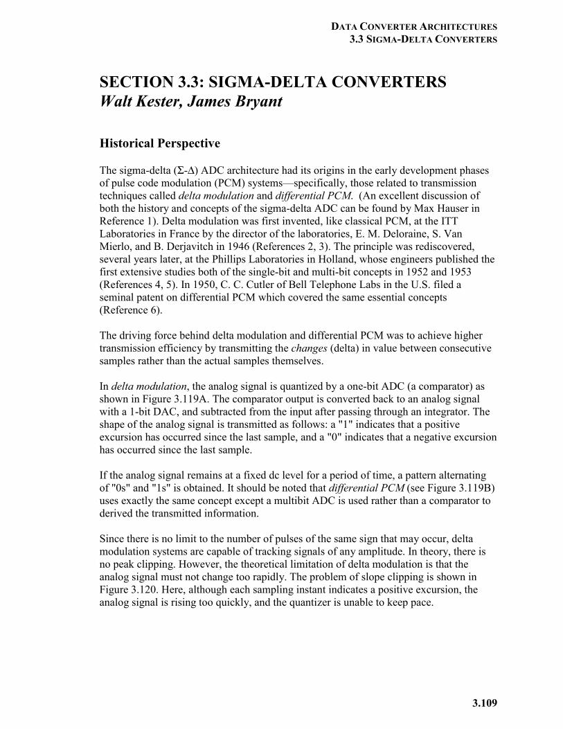
DATA CONVERTER ARCHITECTURES 3.3 SIGMA-DELTA CONVERTERS
3.109
SECTION 3.3: SIGMA-DELTA CONVERTERS Walt Kester, James Bryant Historical Perspective The sigma-delta (Σ-∆) ADC architecture had its origins in the early development phases of pulse code modulation (PCM) systems—specifically, those related to transmission techniques called delta modulation and differential PCM. (An excellent discussion of both the history and concepts of the sigma-delta ADC can be found by Max Hauser in Reference 1). Delta modulation was first invented, like classical PCM, at the ITT Laboratories in France by the director of the laboratories, E. M. Deloraine, S. Van Mierlo, and B. Derjavitch in 1946 (References 2, 3). The principle was rediscovered, several years later, at the Phillips Laboratories in Holland, whose engineers published the first extensive studies both of the single-bit and multi-bit concepts in 1952 and 1953 (References 4, 5). In 1950, C. C. Cutler of Bell Telephone Labs in the U.S. filed a seminal patent on differential PCM which covered the same essential concepts (Reference 6). The driving force behind delta modulation and differential PCM was to achieve higher transmission efficiency by transmitting the changes (delta) in value between consecutive samples rather than the actual samples themselves. In delta modulation, the analog signal is quantized by a one-bit ADC (a comparator) as shown in Figure 3.119A. The comparator output is converted back to an analog signal with a 1-bit DAC, and subtracted from the input after passing through an integrator. The shape of the analog signal is transmitted as follows: a "1" indicates that a positive excursion has occurred since the last sample, and a "0" indicates that a negative excursion has occurred since the last sample. If the analog signal remains at a fixed dc level for a period of time, a pattern alternating of "0s" and "1s" is obtained. It should be noted that differential PCM (see Figure 3.119B) uses exactly the same concept except a multibit ADC is used rather than a comparator to derived the transmitted information. Since there is no limit to the number of pulses of the same sign that may occur, delta modulation systems are capable of tracking signals of any amplitude. In theory, there is no peak clipping. However, the theoretical limitation of delta modulation is that the analog signal must not change too rapidly. The problem of slope clipping is shown in Figure 3.120. Here, although each sampling instant indicates a positive excursion, the analog signal is rising too quickly, and the quantizer is unable to keep pace.
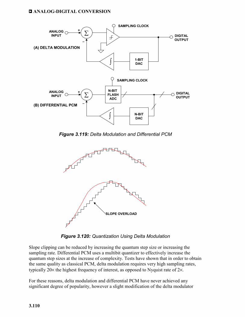
ANALOG-DIGITAL CONVERSION
3.110
Figure 3.119: Delta Modulation and Differential PCM
Figure 3.120: Quantization Using Delta Modulation
Slope clipping can be reduced by increasing the quantum step size or increasing the sampling rate. Differential PCM uses a multibit quantizer to effectively increase the quantum step sizes at the increase of complexity. Tests have shown that in order to obtain the same quality as classical PCM, delta modulation requires very high sampling rates, typically 20× the highest frequency of interest, as opposed to Nyquist rate of 2×. For these reasons, delta modulation and differential PCM have never achieved any significant degree of popularity, however a slight modification of the delta modulator
∑
1-BITDAC
+
–
∑
N-BITDAC∫
+
–
N-BIT FLASH
ADC
ANALOGINPUT
ANALOGINPUT
DIGITALOUTPUT
DIGITALOUTPUT
(A) DELTA MODULATION
(B) DIFFERENTIAL PCM
SAMPLING CLOCK
∫
SAMPLING CLOCK
SLOPE OVERLOAD
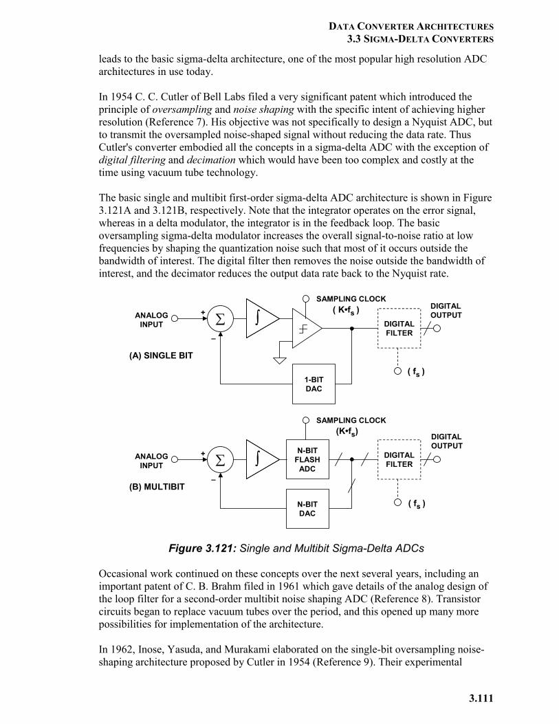
DATA CONVERTER ARCHITECTURES 3.3 SIGMA-DELTA CONVERTERS
3.111
leads to the basic sigma-delta architecture, one of the most popular high resolution ADC architectures in use today. In 1954 C. C. Cutler of Bell Labs filed a very significant patent which introduced the principle of oversampling and noise shaping with the specific intent of achieving higher resolution (Reference 7). His objective was not specifically to design a Nyquist ADC, but to transmit the oversampled noise-shaped signal without reducing the data rate. Thus Cutler's converter embodied all the concepts in a sigma-delta ADC with the exception of digital filtering and decimation which would have been too complex and costly at the time using vacuum tube technology. The basic single and multibit first-order sigma-delta ADC architecture is shown in Figure 3.121A and 3.121B, respectively. Note that the integrator operates on the error signal, whereas in a delta modulator, the integrator is in the feedback loop. The basic oversampling sigma-delta modulator increases the overall signal-to-noise ratio at low frequencies by shaping the quantization noise such that most of it occurs outside the bandwidth of interest. The digital filter then removes the noise outside the bandwidth of interest, and the decimator reduces the output data rate back to the Nyquist rate.
Figure 3.121: Single and Multibit Sigma-Delta ADCs
Occasional work continued on these concepts over the next several years, including an important patent of C. B. Brahm filed in 1961 which gave details of the analog design of the loop filter for a second-order multibit noise shaping ADC (Reference 8). Transistor circuits began to replace vacuum tubes over the period, and this opened up many more possibilities for implementation of the architecture. In 1962, Inose, Yasuda, and Murakami elaborated on the single-bit oversampling noise-shaping architecture proposed by Cutler in 1954 (Reference 9). Their experimental
∑
1-BITDAC
∫∫+
–
ANALOGINPUT
SAMPLING CLOCK
DIGITALFILTER
DIGITALOUTPUT
∑
N-BITDAC
∫∫+
–
ANALOGINPUT
SAMPLING CLOCK
DIGITALFILTER
DIGITALOUTPUTN-BIT
FLASHADC
(A) SINGLE BIT
(B) MULTIBIT
( fs )
( K•fs )
(K•fs)
( fs )
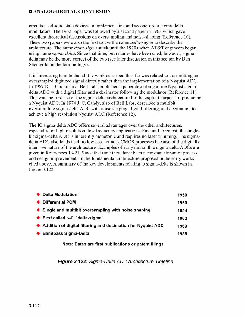
ANALOG-DIGITAL CONVERSION
3.112
circuits used solid state devices to implement first and second-order sigma-delta modulators. The 1962 paper was followed by a second paper in 1963 which gave excellent theoretical discussions on oversampling and noise-shaping (Reference 10). These two papers were also the first to use the name delta-sigma to describe the architecture. The name delta-sigma stuck until the 1970s when AT&T engineers began using name sigma-delta. Since that time, both names have been used; however, sigma-delta may be the more correct of the two (see later discussion in this section by Dan Sheingold on the terminology). It is interesting to note that all the work described thus far was related to transmitting an oversampled digitized signal directly rather than the implementation of a Nyquist ADC. In 1969 D. J. Goodman at Bell Labs published a paper describing a true Nyquist sigma-delta ADC with a digital filter and a decimator following the modulator (Reference 11). This was the first use of the sigma-delta architecture for the explicit purpose of producing a Nyquist ADC. In 1974 J. C. Candy, also of Bell Labs, described a multibit oversampling sigma-delta ADC with noise shaping, digital filtering, and decimation to achieve a high resolution Nyquist ADC (Reference 12). The IC sigma-delta ADC offers several advantages over the other architectures, especially for high resolution, low frequency applications. First and foremost, the single-bit sigma-delta ADC is inherently monotonic and requires no laser trimming. The sigma-delta ADC also lends itself to low cost foundry CMOS processes because of the digitally intensive nature of the architecture. Examples of early monolithic sigma-delta ADCs are given in References 13-21. Since that time there have been a constant stream of process and design improvements in the fundamental architecture proposed in the early works cited above. A summary of the key developments relating to sigma-delta is shown in Figure 3.122.
Figure 3.122: Sigma-Delta ADC Architecture Timeline
Delta Modulation
Differential PCM
Single and multibit oversampling with noise shaping
First called ∆-Σ, "delta-sigma"
Addition of digital filtering and decimation for Nyquist ADC
Bandpass Sigma-Delta
1950
1950
1954
1962
1969
1988
Note: Dates are first publications or patent filings
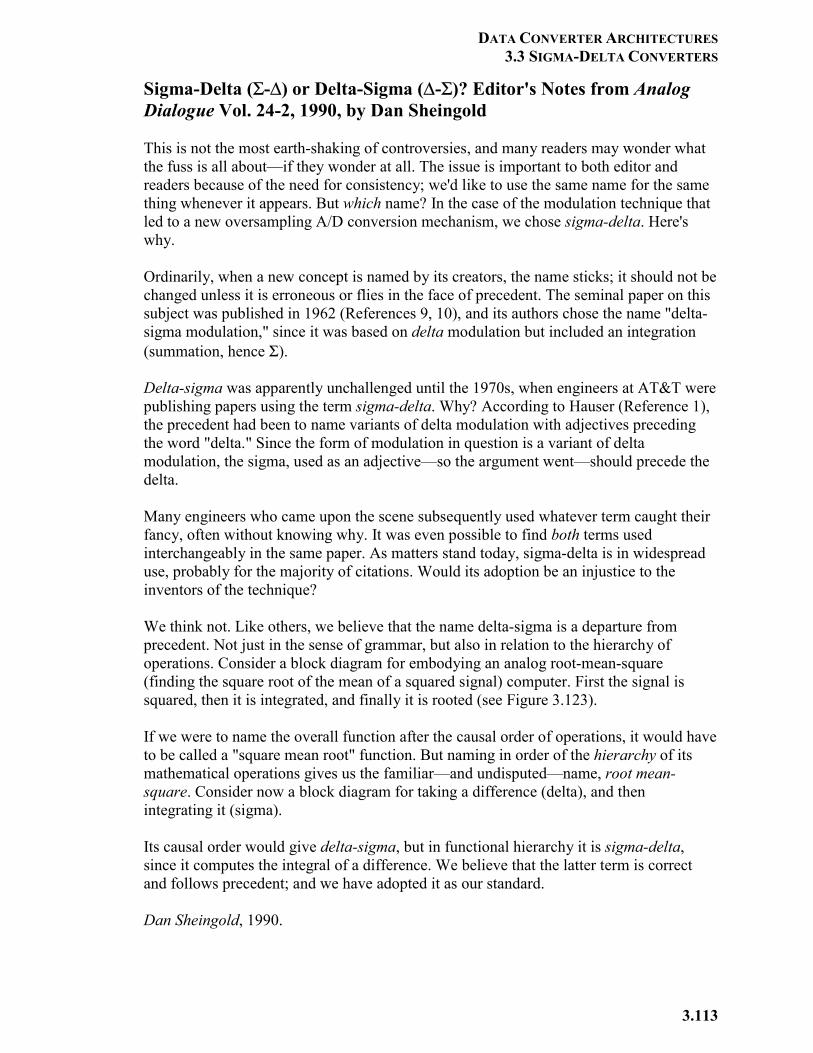
DATA CONVERTER ARCHITECTURES 3.3 SIGMA-DELTA CONVERTERS
3.113
Sigma-Delta (Σ-∆) or Delta-Sigma (∆-Σ)? Editor's Notes from Analog Dialogue Vol. 24-2, 1990, by Dan Sheingold This is not the most earth-shaking of controversies, and many readers may wonder what the fuss is all about—if they wonder at all. The issue is important to both editor and readers because of the need for consistency; we'd like to use the same name for the same thing whenever it appears. But which name? In the case of the modulation technique that led to a new oversampling A/D conversion mechanism, we chose sigma-delta. Here's why. Ordinarily, when a new concept is named by its creators, the name sticks; it should not be changed unless it is erroneous or flies in the face of precedent. The seminal paper on this subject was published in 1962 (References 9, 10), and its authors chose the name "delta-sigma modulation," since it was based on delta modulation but included an integration (summation, hence Σ). Delta-sigma was apparently unchallenged until the 1970s, when engineers at AT&T were publishing papers using the term sigma-delta. Why? According to Hauser (Reference 1), the precedent had been to name variants of delta modulation with adjectives preceding the word "delta." Since the form of modulation in question is a variant of delta modulation, the sigma, used as an adjective—so the argument went—should precede the delta. Many engineers who came upon the scene subsequently used whatever term caught their fancy, often without knowing why. It was even possible to find both terms used interchangeably in the same paper. As matters stand today, sigma-delta is in widespread use, probably for the majority of citations. Would its adoption be an injustice to the inventors of the technique? We think not. Like others, we believe that the name delta-sigma is a departure from precedent. Not just in the sense of grammar, but also in relation to the hierarchy of operations. Consider a block diagram for embodying an analog root-mean-square (finding the square root of the mean of a squared signal) computer. First the signal is squared, then it is integrated, and finally it is rooted (see Figure 3.123). If we were to name the overall function after the causal order of operations, it would have to be called a "square mean root" function. But naming in order of the hierarchy of its mathematical operations gives us the familiar—and undisputed—name, root mean-square. Consider now a block diagram for taking a difference (delta), and then integrating it (sigma). Its causal order would give delta-sigma, but in functional hierarchy it is sigma-delta, since it computes the integral of a difference. We believe that the latter term is correct and follows precedent; and we have adopted it as our standard. Dan Sheingold, 1990.
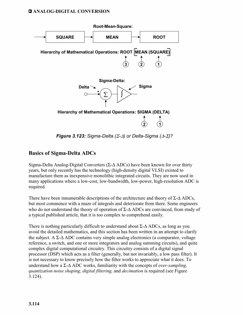
ANALOG-DIGITAL CONVERSION
3.114
Figure 3.123: Sigma-Delta (Σ-∆) or Delta-Sigma (∆-Σ)?
Basics of Sigma-Delta ADCs Sigma-Delta Analog-Digital Converters (Σ-∆ ADCs) have been known for over thirty years, but only recently has the technology (high-density digital VLSI) existed to manufacture them as inexpensive monolithic integrated circuits. They are now used in many applications where a low-cost, low-bandwidth, low-power, high-resolution ADC is required. There have been innumerable descriptions of the architecture and theory of Σ-∆ ADCs, but most commence with a maze of integrals and deteriorate from there. Some engineers who do not understand the theory of operation of Σ-∆ ADCs are convinced, from study of a typical published article, that it is too complex to comprehend easily. There is nothing particularly difficult to understand about Σ-∆ ADCs, as long as you avoid the detailed mathematics, and this section has been written in an attempt to clarify the subject. A Σ-∆ ADC contains very simple analog electronics (a comparator, voltage reference, a switch, and one or more integrators and analog summing circuits), and quite complex digital computational circuitry. This circuitry consists of a digital signal processor (DSP) which acts as a filter (generally, but not invariably, a low pass filter). It is not necessary to know precisely how the filter works to appreciate what it does. To understand how a Σ-∆ ADC works, familiarity with the concepts of over-sampling, quantization noise shaping, digital filtering, and decimation is required (see Figure 3.124).
Root-Mean-Square:
SQUARE MEAN ROOT
Hierarchy of Mathematical Operations: ROOT MEAN (SQUARE)
123
∑ ∫∫+
Sigma-Delta:
Hierarchy of Mathematical Operations: SIGMA (DELTA)
12
Delta Sigma
DATA CONVERTER ARCHITECTURES 3.3 SIGMA-DELTA CONVERTERS
3.115
Figure 3.124: Sigma-Delta ADCs
Let us consider the technique of over-sampling with an analysis in the frequency domain. Where a dc conversion has a quantization error of up to ½ LSB, a sampled data system has quantization noise. A perfect classical N-bit sampling ADC has an rms quantization noise of q/√12 uniformly distributed within the Nyquist band of dc to fs/2 (where q is the value of an LSB and fs is the sampling rate) as shown in Figure 3.125A. Therefore, its SNR with a full-scale sinewave input will be (6.02N + 1.76) dB. If the ADC is less than perfect, and its noise is greater than its theoretical minimum quantization noise, then its effective resolution will be less than N-bits. Its actual resolution (often known as its Effective Number of Bits or ENOB) will be defined by
dB02.6
dB76.1SNRENOB −= . Eq. 3.16
If we choose a much higher sampling rate, Kfs (see Figure 3.125B), the rms quantization noise remains q/√12, but the noise is now distributed over a wider bandwidth dc to Kfs/2. If we then apply a digital low pass filter (LPF) to the output, we remove much of the quantization noise, but do not affect the wanted signal—so the ENOB is improved. We have accomplished a high resolution A/D conversion with a low resolution ADC. The factor K is generally referred to as the oversampling ratio. It should be noted at this point that oversampling has an added benefit in that it relaxes the requirements on the analog antialiasing filter.
Low Cost, High Resolution (to 24-bits)
Excellent DNL
Low Power, but Limited Bandwidth (Voiceband, Audio)
Key Concepts are Simple, but Math is Complex
Oversampling
Quantization Noise Shaping
Digital Filtering
Decimation
Ideal for Sensor Signal Conditioning
High Resolution
Self, System, and Auto Calibration Modes
Wide Applications in Voiceband and Audio Signal Processing
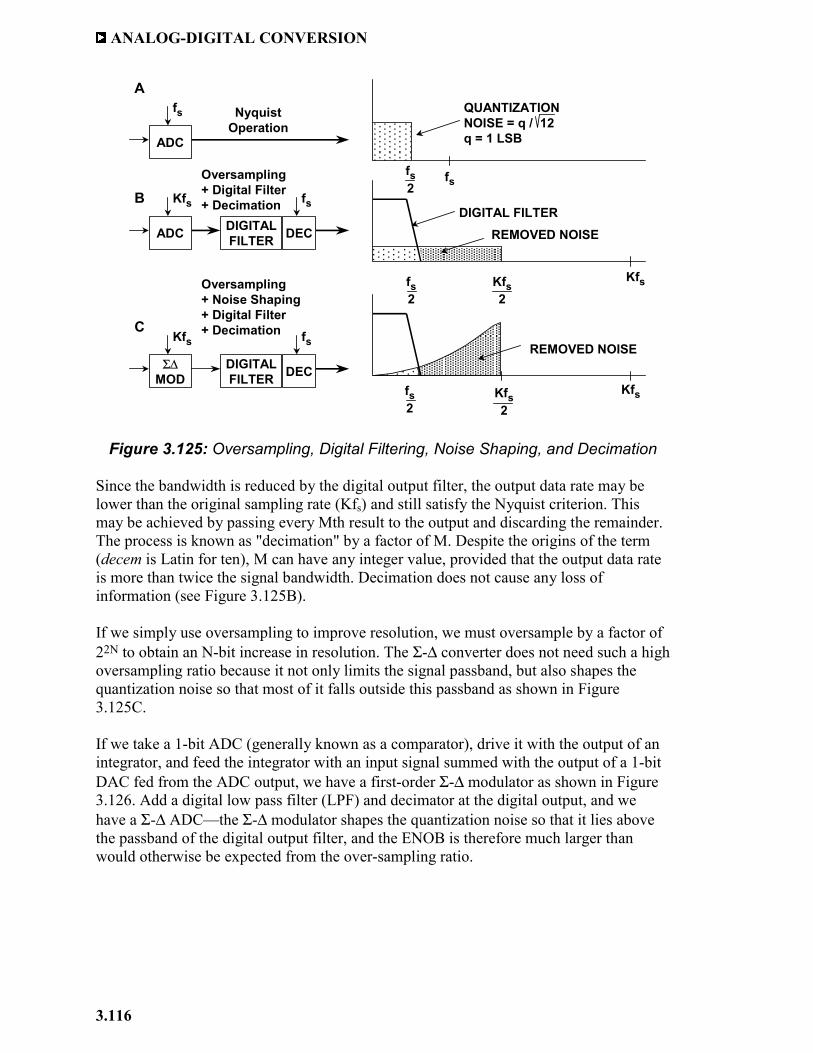
ANALOG-DIGITAL CONVERSION
3.116
Figure 3.125: Oversampling, Digital Filtering, Noise Shaping, and Decimation
Since the bandwidth is reduced by the digital output filter, the output data rate may be lower than the original sampling rate (Kfs) and still satisfy the Nyquist criterion. This may be achieved by passing every Mth result to the output and discarding the remainder. The process is known as "decimation" by a factor of M. Despite the origins of the term (decem is Latin for ten), M can have any integer value, provided that the output data rate is more than twice the signal bandwidth. Decimation does not cause any loss of information (see Figure 3.125B). If we simply use oversampling to improve resolution, we must oversample by a factor of 22N to obtain an N-bit increase in resolution. The Σ-∆ converter does not need such a high oversampling ratio because it not only limits the signal passband, but also shapes the quantization noise so that most of it falls outside this passband as shown in Figure 3.125C. If we take a 1-bit ADC (generally known as a comparator), drive it with the output of an integrator, and feed the integrator with an input signal summed with the output of a 1-bit DAC fed from the ADC output, we have a first-order Σ-∆ modulator as shown in Figure 3.126. Add a digital low pass filter (LPF) and decimator at the digital output, and we have a Σ-∆ ADC—the Σ-∆ modulator shapes the quantization noise so that it lies above the passband of the digital output filter, and the ENOB is therefore much larger than would otherwise be expected from the over-sampling ratio.
fs2
fs
Kfs2
Kfs
KfsKfs2
fs2
fs2
DIGITAL FILTERREMOVED NOISE
REMOVED NOISE
QUANTIZATIONNOISE = q / 12 q = 1 LSBADC
ADC DIGITALFILTER
Σ∆MOD
DIGITALFILTER
fs
Kfs
Kfs
DEC
fs
NyquistOperation
Oversampling+ Digital Filter+ Decimation
Oversampling+ Noise Shaping+ Digital Filter+ Decimation
A
B
C
DEC
fs
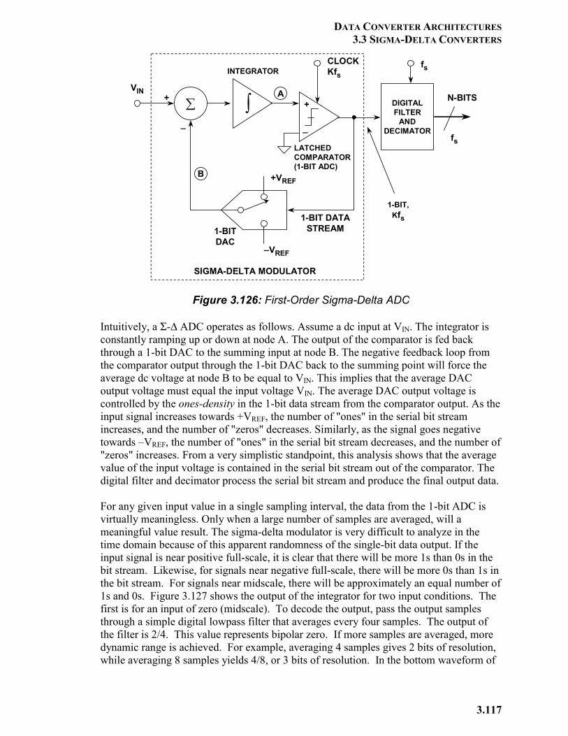
DATA CONVERTER ARCHITECTURES 3.3 SIGMA-DELTA CONVERTERS
3.117
Figure 3.126: First-Order Sigma-Delta ADC
Intuitively, a Σ-∆ ADC operates as follows. Assume a dc input at VIN. The integrator is constantly ramping up or down at node A. The output of the comparator is fed back through a 1-bit DAC to the summing input at node B. The negative feedback loop from the comparator output through the 1-bit DAC back to the summing point will force the average dc voltage at node B to be equal to VIN. This implies that the average DAC output voltage must equal the input voltage VIN. The average DAC output voltage is controlled by the ones-density in the 1-bit data stream from the comparator output. As the input signal increases towards +VREF, the number of "ones" in the serial bit stream increases, and the number of "zeros" decreases. Similarly, as the signal goes negative towards –VREF, the number of "ones" in the serial bit stream decreases, and the number of "zeros" increases. From a very simplistic standpoint, this analysis shows that the average value of the input voltage is contained in the serial bit stream out of the comparator. The digital filter and decimator process the serial bit stream and produce the final output data. For any given input value in a single sampling interval, the data from the 1-bit ADC is virtually meaningless. Only when a large number of samples are averaged, will a meaningful value result. The sigma-delta modulator is very difficult to analyze in the time domain because of this apparent randomness of the single-bit data output. If the input signal is near positive full-scale, it is clear that there will be more 1s than 0s in the bit stream. Likewise, for signals near negative full-scale, there will be more 0s than 1s in the bit stream. For signals near midscale, there will be approximately an equal number of 1s and 0s. Figure 3.127 shows the output of the integrator for two input conditions. The first is for an input of zero (midscale). To decode the output, pass the output samples through a simple digital lowpass filter that averages every four samples. The output of the filter is 2/4. This value represents bipolar zero. If more samples are averaged, more dynamic range is achieved. For example, averaging 4 samples gives 2 bits of resolution, while averaging 8 samples yields 4/8, or 3 bits of resolution. In the bottom waveform of
∑ ∫ +
_
+VREF
–VREF
DIGITALFILTER
ANDDECIMATOR
+
_
CLOCKKfs
VINN-BITS
fs
fs
A
B
1-BIT DATASTREAM1-BIT
DAC
LATCHEDCOMPARATOR(1-BIT ADC)
1-BIT,Kfs
SIGMA-DELTA MODULATOR
INTEGRATOR
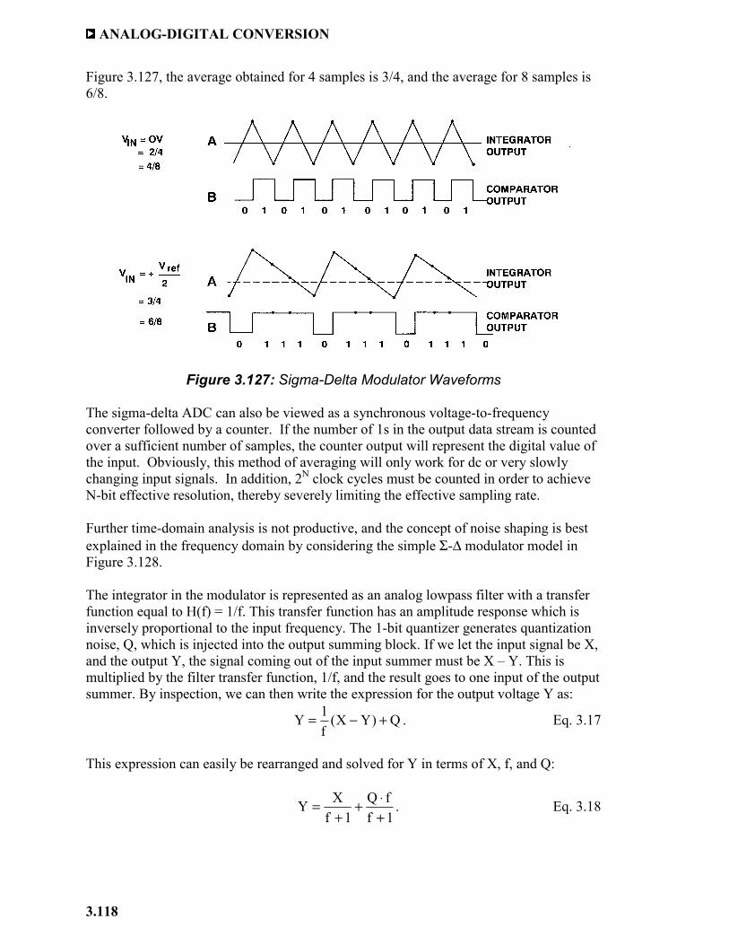
ANALOG-DIGITAL CONVERSION
3.118
Figure 3.127, the average obtained for 4 samples is 3/4, and the average for 8 samples is 6/8.
Figure 3.127: Sigma-Delta Modulator Waveforms
The sigma-delta ADC can also be viewed as a synchronous voltage-to-frequency converter followed by a counter. If the number of 1s in the output data stream is counted over a sufficient number of samples, the counter output will represent the digital value of the input. Obviously, this method of averaging will only work for dc or very slowly changing input signals. In addition, 2N clock cycles must be counted in order to achieve N-bit effective resolution, thereby severely limiting the effective sampling rate. Further time-domain analysis is not productive, and the concept of noise shaping is best explained in the frequency domain by considering the simple Σ-∆ modulator model in Figure 3.128. The integrator in the modulator is represented as an analog lowpass filter with a transfer function equal to H(f) = 1/f. This transfer function has an amplitude response which is inversely proportional to the input frequency. The 1-bit quantizer generates quantization noise, Q, which is injected into the output summing block. If we let the input signal be X, and the output Y, the signal coming out of the input summer must be X – Y. This is multiplied by the filter transfer function, 1/f, and the result goes to one input of the output summer. By inspection, we can then write the expression for the output voltage Y as:
Q)YX(f1Y +−= . Eq. 3.17
This expression can easily be rearranged and solved for Y in terms of X, f, and Q:
1ffQ
1fXY
+⋅+
+= . Eq. 3.18
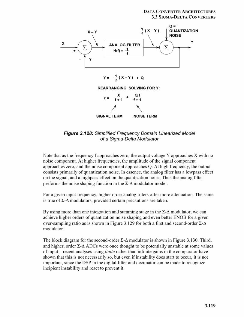
DATA CONVERTER ARCHITECTURES 3.3 SIGMA-DELTA CONVERTERS
3.119
Figure 3.128: Simplified Frequency Domain Linearized Model of a Sigma-Delta Modulator
Note that as the frequency f approaches zero, the output voltage Y approaches X with no noise component. At higher frequencies, the amplitude of the signal component approaches zero, and the noise component approaches Q. At high frequency, the output consists primarily of quantization noise. In essence, the analog filter has a lowpass effect on the signal, and a highpass effect on the quantization noise. Thus the analog filter performs the noise shaping function in the Σ-∆ modulator model. For a given input frequency, higher order analog filters offer more attenuation. The same is true of Σ-∆ modulators, provided certain precautions are taken. By using more than one integration and summing stage in the Σ-∆ modulator, we can achieve higher orders of quantization noise shaping and even better ENOB for a given over-sampling ratio as is shown in Figure 3.129 for both a first and second-order Σ-∆ modulator. The block diagram for the second-order Σ-∆ modulator is shown in Figure 3.130. Third, and higher, order Σ-∆ ADCs were once thought to be potentially unstable at some values of input—recent analyses using finite rather than infinite gains in the comparator have shown that this is not necessarily so, but even if instability does start to occur, it is not important, since the DSP in the digital filter and decimator can be made to recognize incipient instability and react to prevent it.
∑ ANALOG FILTERH(f) = 1
f∑
X Y
+
_
X – Y1f
( X – Y )Q = QUANTIZATIONNOISE
Y = 1f
( X – Y ) + Q
REARRANGING, SOLVING FOR Y:
Y = X
f + 1 + Q ff + 1
SIGNAL TERM NOISE TERM
Y
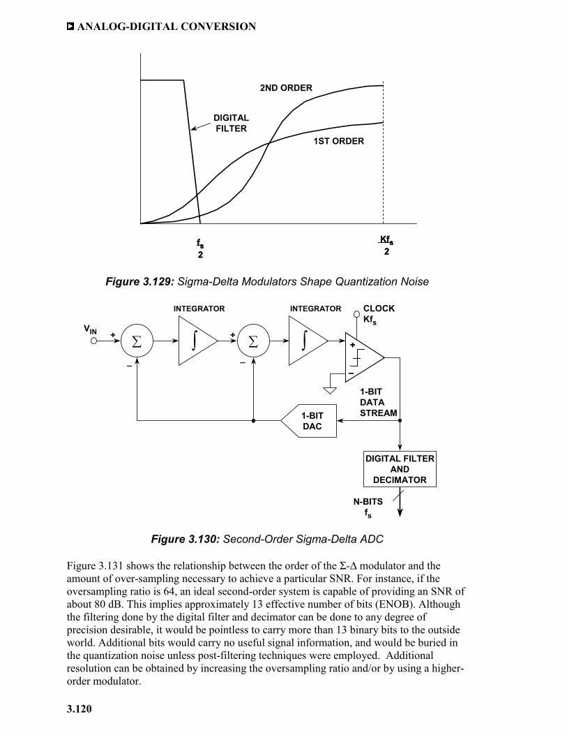
ANALOG-DIGITAL CONVERSION
3.120
Figure 3.129: Sigma-Delta Modulators Shape Quantization Noise
Figure 3.130: Second-Order Sigma-Delta ADC
Figure 3.131 shows the relationship between the order of the Σ-∆ modulator and the amount of over-sampling necessary to achieve a particular SNR. For instance, if the oversampling ratio is 64, an ideal second-order system is capable of providing an SNR of about 80 dB. This implies approximately 13 effective number of bits (ENOB). Although the filtering done by the digital filter and decimator can be done to any degree of precision desirable, it would be pointless to carry more than 13 binary bits to the outside world. Additional bits would carry no useful signal information, and would be buried in the quantization noise unless post-filtering techniques were employed. Additional resolution can be obtained by increasing the oversampling ratio and/or by using a higher-order modulator.
fs2fs2
Kfs2
Kfs2
2ND ORDER
1ST ORDER
DIGITALFILTER
∑ ∫+
_
VIN
INTEGRATOR
∑ ∫ +
_
+
_
CLOCKKfs
1-BITDAC
INTEGRATOR
DIGITAL FILTERAND
DECIMATOR
N-BITSfs
+
_
1-BITDATASTREAM
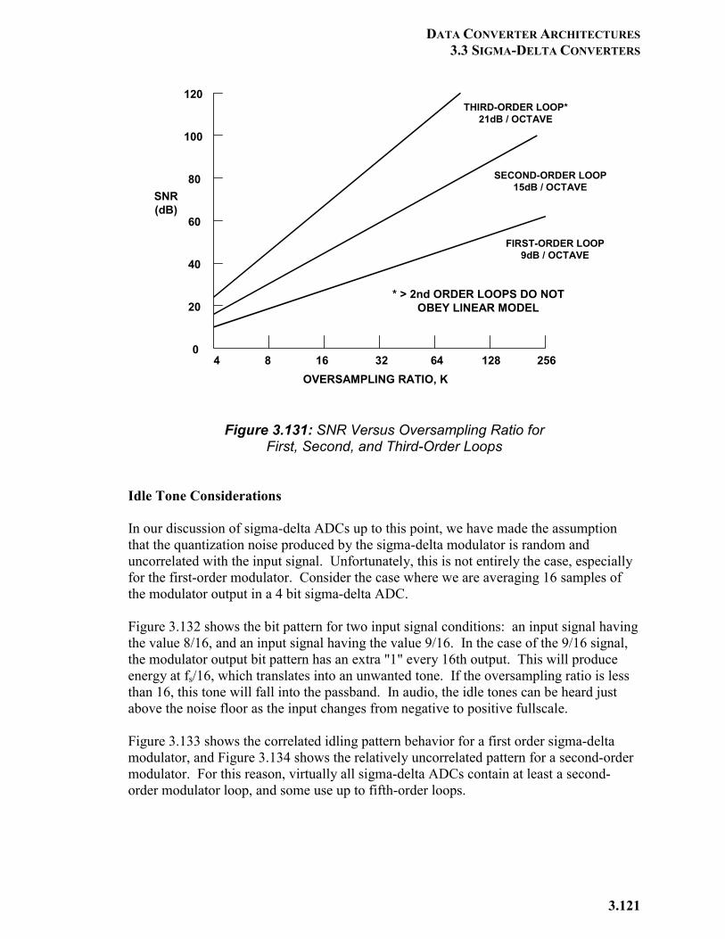
DATA CONVERTER ARCHITECTURES 3.3 SIGMA-DELTA CONVERTERS
3.121
Figure 3.131: SNR Versus Oversampling Ratio for First, Second, and Third-Order Loops
Idle Tone Considerations In our discussion of sigma-delta ADCs up to this point, we have made the assumption that the quantization noise produced by the sigma-delta modulator is random and uncorrelated with the input signal. Unfortunately, this is not entirely the case, especially for the first-order modulator. Consider the case where we are averaging 16 samples of the modulator output in a 4 bit sigma-delta ADC. Figure 3.132 shows the bit pattern for two input signal conditions: an input signal having the value 8/16, and an input signal having the value 9/16. In the case of the 9/16 signal, the modulator output bit pattern has an extra "1" every 16th output. This will produce energy at fs/16, which translates into an unwanted tone. If the oversampling ratio is less than 16, this tone will fall into the passband. In audio, the idle tones can be heard just above the noise floor as the input changes from negative to positive fullscale. Figure 3.133 shows the correlated idling pattern behavior for a first order sigma-delta modulator, and Figure 3.134 shows the relatively uncorrelated pattern for a second-order modulator. For this reason, virtually all sigma-delta ADCs contain at least a second-order modulator loop, and some use up to fifth-order loops.
FIRST-ORDER LOOP9dB / OCTAVE
SECOND-ORDER LOOP15dB / OCTAVE
THIRD-ORDER LOOP*21dB / OCTAVE
* > 2nd ORDER LOOPS DO NOTOBEY LINEAR MODEL
4 8 16 32 64 128 2560
20
40
60
80
100
120
SNR(dB)
OVERSAMPLING RATIO, K
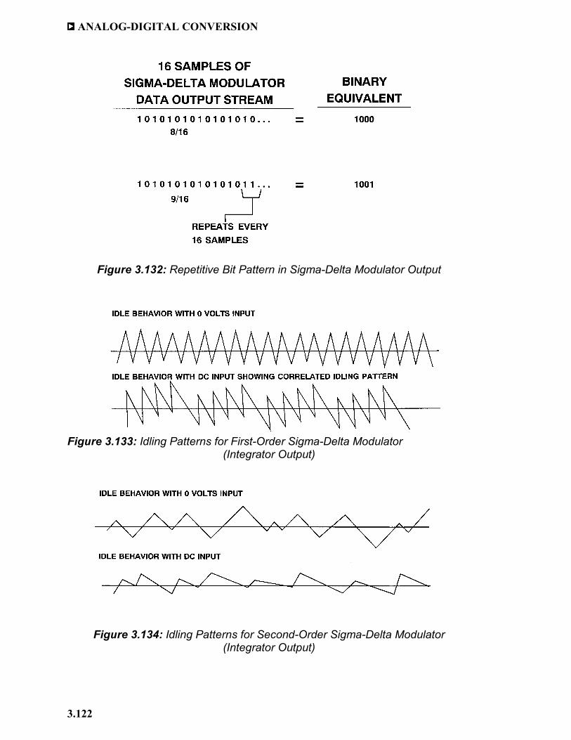
ANALOG-DIGITAL CONVERSION
3.122
Figure 3.132: Repetitive Bit Pattern in Sigma-Delta Modulator Output
Figure 3.133: Idling Patterns for First-Order Sigma-Delta Modulator (Integrator Output)
Figure 3.134: Idling Patterns for Second-Order Sigma-Delta Modulator (Integrator Output)
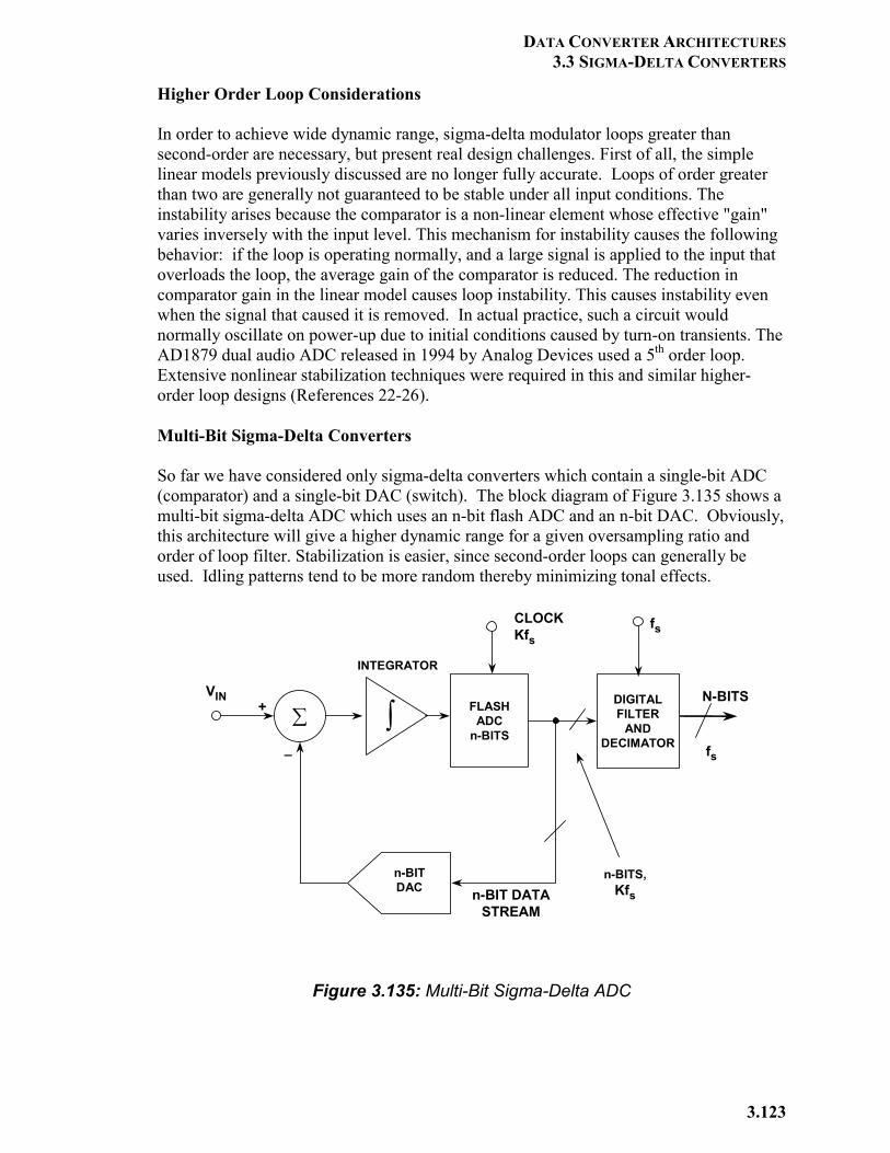
DATA CONVERTER ARCHITECTURES 3.3 SIGMA-DELTA CONVERTERS
3.123
Higher Order Loop Considerations In order to achieve wide dynamic range, sigma-delta modulator loops greater than second-order are necessary, but present real design challenges. First of all, the simple linear models previously discussed are no longer fully accurate. Loops of order greater than two are generally not guaranteed to be stable under all input conditions. The instability arises because the comparator is a non-linear element whose effective "gain" varies inversely with the input level. This mechanism for instability causes the following behavior: if the loop is operating normally, and a large signal is applied to the input that overloads the loop, the average gain of the comparator is reduced. The reduction in comparator gain in the linear model causes loop instability. This causes instability even when the signal that caused it is removed. In actual practice, such a circuit would normally oscillate on power-up due to initial conditions caused by turn-on transients. The AD1879 dual audio ADC released in 1994 by Analog Devices used a 5th order loop. Extensive nonlinear stabilization techniques were required in this and similar higher-order loop designs (References 22-26). Multi-Bit Sigma-Delta Converters So far we have considered only sigma-delta converters which contain a single-bit ADC (comparator) and a single-bit DAC (switch). The block diagram of Figure 3.135 shows a multi-bit sigma-delta ADC which uses an n-bit flash ADC and an n-bit DAC. Obviously, this architecture will give a higher dynamic range for a given oversampling ratio and order of loop filter. Stabilization is easier, since second-order loops can generally be used. Idling patterns tend to be more random thereby minimizing tonal effects.
Figure 3.135: Multi-Bit Sigma-Delta ADC
∑ ∫DIGITALFILTER
ANDDECIMATOR
+
_
CLOCKKfs
VIN N-BITS
fs
fs
n-BIT DATASTREAM
n-BITS,Kfs
INTEGRATOR
FLASHADC
n-BITS
n-BITDAC
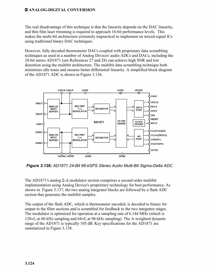
ANALOG-DIGITAL CONVERSION
3.124
The real disadvantage of this technique is that the linearity depends on the DAC linearity, and thin film laser trimming is required to approach 16-bit performance levels. This makes the multi-bit architecture extremely impractical to implement on mixed-signal ICs using traditional binary DAC techniques. However, fully decoded thermometer DACs coupled with proprietary data scrambling techniques as used in a number of Analog Devices' audio ADCs and DACs, including the 24-bit stereo AD1871 (see References 27 and 28) can achieve high SNR and low distortion using the multibit architecture. The multibit data scrambling technique both minimizes idle tones and ensures better differential linearity. A simplified block diagram of the AD1871 ADC is shown in Figure 3.136.
Figure 3.136: AD1871 24-Bit 96-kSPS Stereo Audio Multi-Bit Sigma-Delta ADC
The AD1871's analog Σ-∆ modulator section comprises a second order multibit implementation using Analog Device's proprietary technology for best performance. As shown in Figure 3.137, the two analog integrator blocks are followed by a flash ADC section that generates the multibit samples. The output of the flash ADC, which is thermometer encoded, is decoded to binary for output to the filter sections and is scrambled for feedback to the two integrator stages. The modulator is optimized for operation at a sampling rate of 6.144 MHz (which is 128×fs at 48-kHz sampling and 64×fs at 96-kHz sampling). The A-weighted dynamic range of the AD1871 is typically 105 dB. Key specifications for the AD1871 are summarized in Figure 3.138.
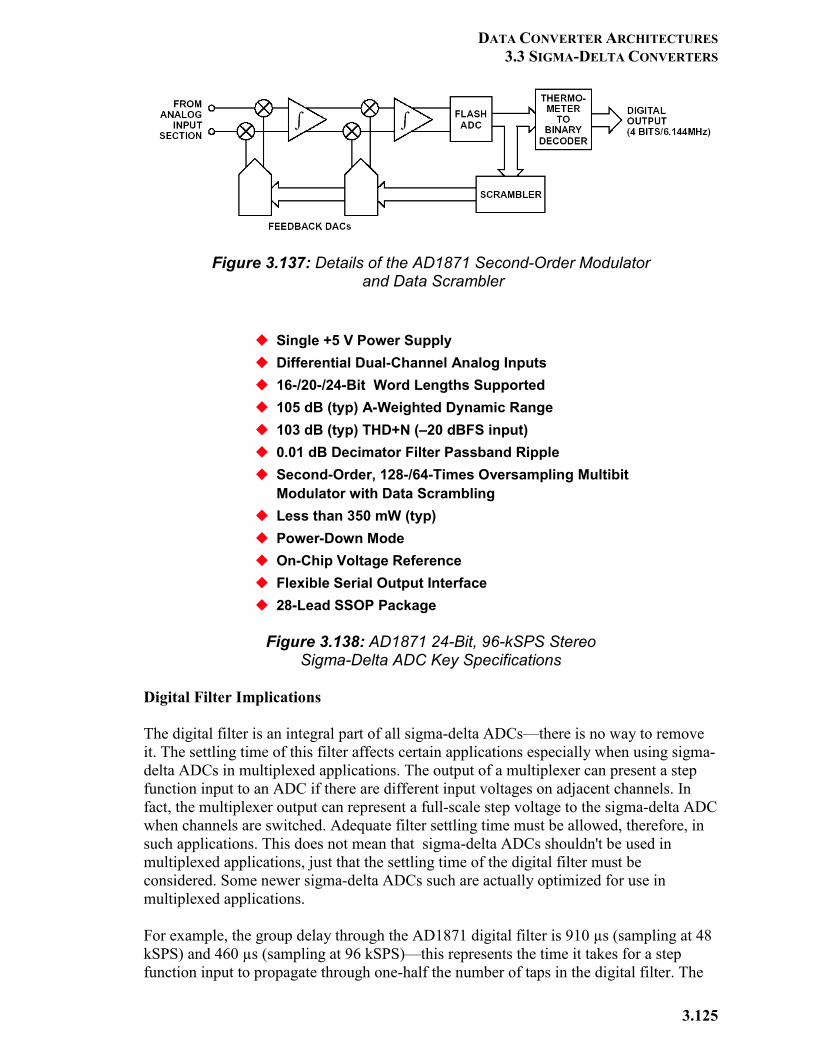
DATA CONVERTER ARCHITECTURES 3.3 SIGMA-DELTA CONVERTERS
3.125
Figure 3.137: Details of the AD1871 Second-Order Modulator
and Data Scrambler
Figure 3.138: AD1871 24-Bit, 96-kSPS Stereo
Sigma-Delta ADC Key Specifications Digital Filter Implications The digital filter is an integral part of all sigma-delta ADCs—there is no way to remove it. The settling time of this filter affects certain applications especially when using sigma-delta ADCs in multiplexed applications. The output of a multiplexer can present a step function input to an ADC if there are different input voltages on adjacent channels. In fact, the multiplexer output can represent a full-scale step voltage to the sigma-delta ADC when channels are switched. Adequate filter settling time must be allowed, therefore, in such applications. This does not mean that sigma-delta ADCs shouldn't be used in multiplexed applications, just that the settling time of the digital filter must be considered. Some newer sigma-delta ADCs such are actually optimized for use in multiplexed applications. For example, the group delay through the AD1871 digital filter is 910 µs (sampling at 48 kSPS) and 460 µs (sampling at 96 kSPS)—this represents the time it takes for a step function input to propagate through one-half the number of taps in the digital filter. The
Single +5 V Power SupplyDifferential Dual-Channel Analog Inputs16-/20-/24-Bit Word Lengths Supported105 dB (typ) A-Weighted Dynamic Range103 dB (typ) THD+N (–20 dBFS input)0.01 dB Decimator Filter Passband RippleSecond-Order, 128-/64-Times Oversampling Multibit Modulator with Data ScramblingLess than 350 mW (typ) Power-Down ModeOn-Chip Voltage ReferenceFlexible Serial Output Interface28-Lead SSOP Package
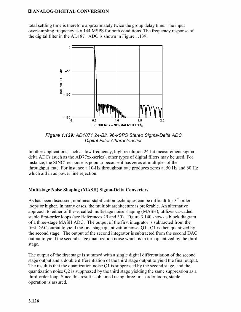
ANALOG-DIGITAL CONVERSION
3.126
total settling time is therefore approximately twice the group delay time. The input oversampling frequency is 6.144 MSPS for both conditions. The frequency response of the digital filter in the AD1871 ADC is shown in Figure 1.139.
Figure 1.139: AD1871 24-Bit, 96-kSPS Stereo Sigma-Delta ADC
Digital Filter Characteristics In other applications, such as low frequency, high resolution 24-bit measurement sigma-delta ADCs (such as the AD77xx-series), other types of digital filters may be used. For instance, the SINC3 response is popular because it has zeros at multiples of the throughput rate. For instance a 10-Hz throughput rate produces zeros at 50 Hz and 60 Hz which aid in ac power line rejection. Multistage Noise Shaping (MASH) Sigma-Delta Converters As has been discussed, nonlinear stabilization techniques can be difficult for 3rd order loops or higher. In many cases, the multibit architecture is preferable. An alternative approach to either of these, called multistage noise shaping (MASH), utilizes cascaded stable first-order loops (see References 29 and 30). Figure 3.140 shows a block diagram of a three-stage MASH ADC. The output of the first integrator is subtracted from the first DAC output to yield the first stage quantization noise, Q1. Q1 is then quantized by the second stage. The output of the second integrator is subtracted from the second DAC output to yield the second stage quantization noise which is in turn quantized by the third stage. The output of the first stage is summed with a single digital differentiation of the second stage output and a double differentiation of the third stage output to yield the final output. The result is that the quantization noise Q1 is suppressed by the second stage, and the quantization noise Q2 is suppressed by the third stage yielding the same suppression as a third-order loop. Since this result is obtained using three first-order loops, stable operation is assured.
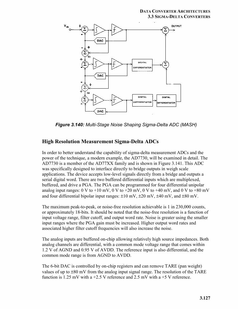
DATA CONVERTER ARCHITECTURES 3.3 SIGMA-DELTA CONVERTERS
3.127
Figure 3.140: Multi-Stage Noise Shaping Sigma-Delta ADC (MASH)
High Resolution Measurement Sigma-Delta ADCs In order to better understand the capability of sigma-delta measurement ADCs and the power of the technique, a modern example, the AD7730, will be examined in detail. The AD7730 is a member of the AD77XX family and is shown in Figure 3.141. This ADC was specifically designed to interface directly to bridge outputs in weigh scale applications. The device accepts low-level signals directly from a bridge and outputs a serial digital word. There are two buffered differential inputs which are multiplexed, buffered, and drive a PGA. The PGA can be programmed for four differential unipolar analog input ranges: 0 V to +10 mV, 0 V to +20 mV, 0 V to +40 mV, and 0 V to +80 mV and four differential bipolar input ranges: ±10 mV, ±20 mV, ±40 mV, and ±80 mV. The maximum peak-to-peak, or noise-free resolution achievable is 1 in 230,000 counts, or approximately 18-bits. It should be noted that the noise-free resolution is a function of input voltage range, filter cutoff, and output word rate. Noise is greater using the smaller input ranges where the PGA gain must be increased. Higher output word rates and associated higher filter cutoff frequencies will also increase the noise. The analog inputs are buffered on-chip allowing relatively high source impedances. Both analog channels are differential, with a common mode voltage range that comes within 1.2 V of AGND and 0.95 V of AVDD. The reference input is also differential, and the common mode range is from AGND to AVDD. The 6-bit DAC is controlled by on-chip registers and can remove TARE (pan weight) values of up to ±80 mV from the analog input signal range. The resolution of the TARE function is 1.25 mV with a +2.5 V reference and 2.5 mV with a +5 V reference.
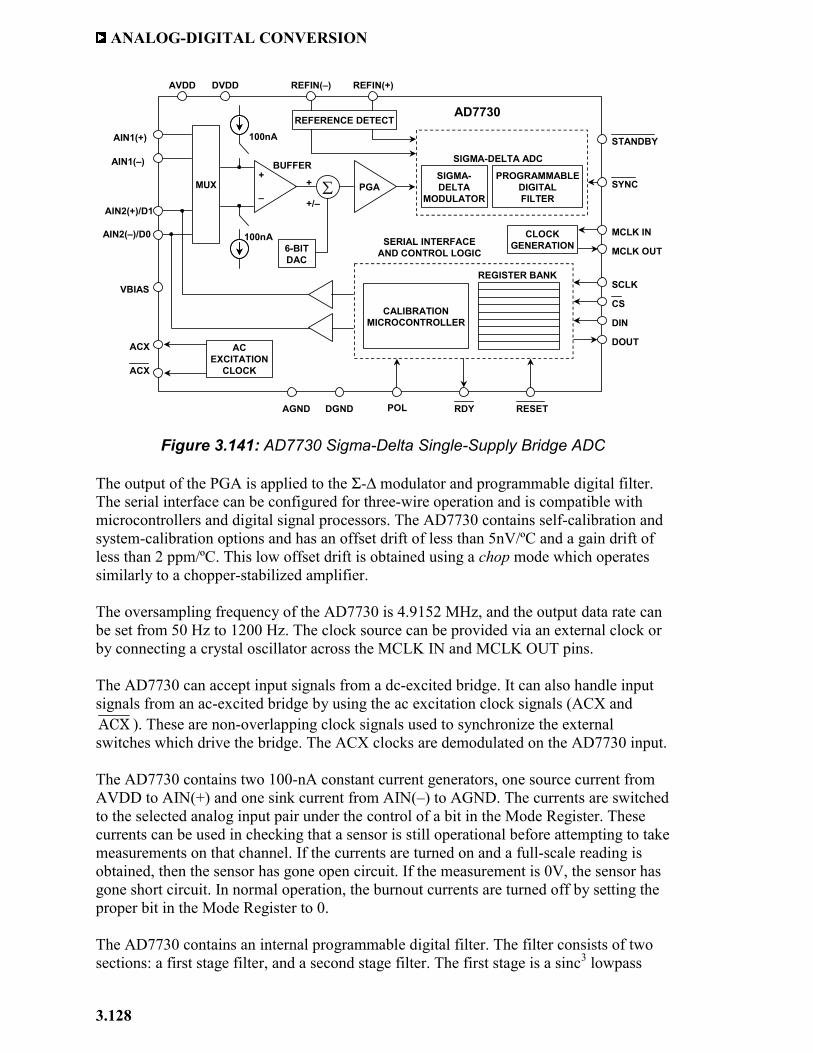
ANALOG-DIGITAL CONVERSION
3.128
Figure 3.141: AD7730 Sigma-Delta Single-Supply Bridge ADC
The output of the PGA is applied to the Σ-∆ modulator and programmable digital filter. The serial interface can be configured for three-wire operation and is compatible with microcontrollers and digital signal processors. The AD7730 contains self-calibration and system-calibration options and has an offset drift of less than 5nV/ºC and a gain drift of less than 2 ppm/ºC. This low offset drift is obtained using a chop mode which operates similarly to a chopper-stabilized amplifier. The oversampling frequency of the AD7730 is 4.9152 MHz, and the output data rate can be set from 50 Hz to 1200 Hz. The clock source can be provided via an external clock or by connecting a crystal oscillator across the MCLK IN and MCLK OUT pins. The AD7730 can accept input signals from a dc-excited bridge. It can also handle input signals from an ac-excited bridge by using the ac excitation clock signals (ACX and ACX ). These are non-overlapping clock signals used to synchronize the external switches which drive the bridge. The ACX clocks are demodulated on the AD7730 input. The AD7730 contains two 100-nA constant current generators, one source current from AVDD to AIN(+) and one sink current from AIN(–) to AGND. The currents are switched to the selected analog input pair under the control of a bit in the Mode Register. These currents can be used in checking that a sensor is still operational before attempting to take measurements on that channel. If the currents are turned on and a full-scale reading is obtained, then the sensor has gone open circuit. If the measurement is 0V, the sensor has gone short circuit. In normal operation, the burnout currents are turned off by setting the proper bit in the Mode Register to 0.
The AD7730 contains an internal programmable digital filter. The filter consists of two sections: a first stage filter, and a second stage filter. The first stage is a sinc3 lowpass
MUX ∑ PGASIGMA-DELTA
MODULATOR
PROGRAMMABLEDIGITALFILTER
REFERENCE DETECT
CALIBRATIONMICROCONTROLLER
6-BITDAC
+
+/–
ACEXCITATION
CLOCK
CLOCKGENERATION
REGISTER BANK
SIGMA-DELTA ADC
SERIAL INTERFACEAND CONTROL LOGIC
VBIAS
AIN1(+)
AIN1(–)
AIN2(+)/D1
AIN2(–)/D0
ACX
ACX
AVDD DVDD REFIN(–) REFIN(+)
STANDBY
SYNC
MCLK IN
MCLK OUT
SCLK
CS
DIN
DOUT
AGND DGND POL RDY RESET
100nA
100nA
BUFFER
AD7730
+
_
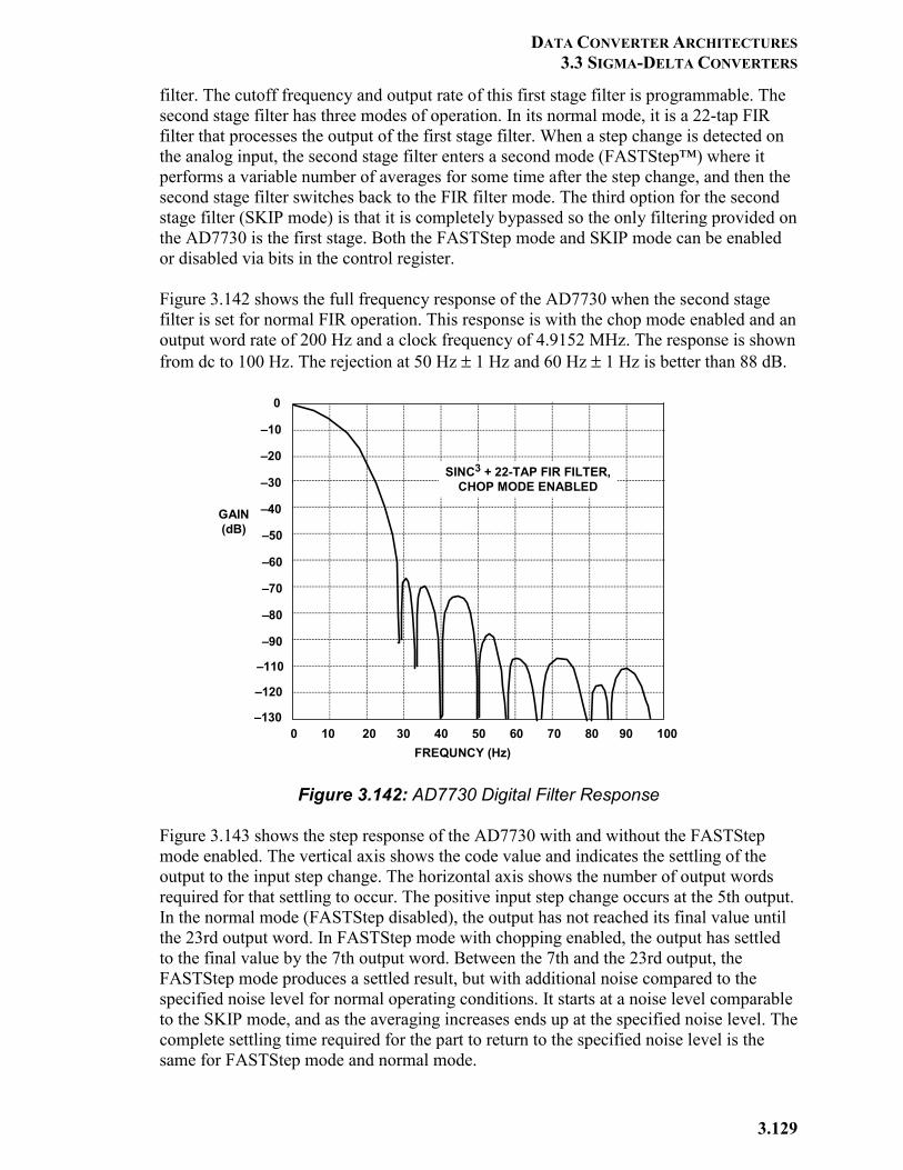
DATA CONVERTER ARCHITECTURES 3.3 SIGMA-DELTA CONVERTERS
3.129
filter. The cutoff frequency and output rate of this first stage filter is programmable. The second stage filter has three modes of operation. In its normal mode, it is a 22-tap FIR filter that processes the output of the first stage filter. When a step change is detected on the analog input, the second stage filter enters a second mode (FASTStep™) where it performs a variable number of averages for some time after the step change, and then the second stage filter switches back to the FIR filter mode. The third option for the second stage filter (SKIP mode) is that it is completely bypassed so the only filtering provided on the AD7730 is the first stage. Both the FASTStep mode and SKIP mode can be enabled or disabled via bits in the control register. Figure 3.142 shows the full frequency response of the AD7730 when the second stage filter is set for normal FIR operation. This response is with the chop mode enabled and an output word rate of 200 Hz and a clock frequency of 4.9152 MHz. The response is shown from dc to 100 Hz. The rejection at 50 Hz ± 1 Hz and 60 Hz ± 1 Hz is better than 88 dB.
Figure 3.142: AD7730 Digital Filter Response
Figure 3.143 shows the step response of the AD7730 with and without the FASTStep mode enabled. The vertical axis shows the code value and indicates the settling of the output to the input step change. The horizontal axis shows the number of output words required for that settling to occur. The positive input step change occurs at the 5th output. In the normal mode (FASTStep disabled), the output has not reached its final value until the 23rd output word. In FASTStep mode with chopping enabled, the output has settled to the final value by the 7th output word. Between the 7th and the 23rd output, the FASTStep mode produces a settled result, but with additional noise compared to the specified noise level for normal operating conditions. It starts at a noise level comparable to the SKIP mode, and as the averaging increases ends up at the specified noise level. The complete settling time required for the part to return to the specified noise level is the same for FASTStep mode and normal mode.
0
–10
–20
–30
–40
–50
–60
–70
–80
–90
–110
–120
–1300 10 20 30 40 50 60 70 80 90 100
GAIN(dB)
FREQUNCY (Hz)
SINC3 + 22-TAP FIR FILTER,CHOP MODE ENABLED
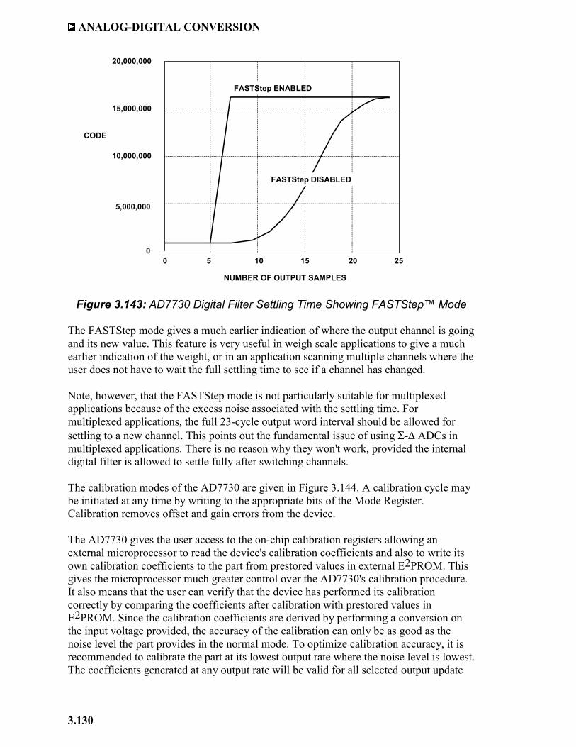
ANALOG-DIGITAL CONVERSION
3.130
Figure 3.143: AD7730 Digital Filter Settling Time Showing FASTStep™ Mode
The FASTStep mode gives a much earlier indication of where the output channel is going and its new value. This feature is very useful in weigh scale applications to give a much earlier indication of the weight, or in an application scanning multiple channels where the user does not have to wait the full settling time to see if a channel has changed. Note, however, that the FASTStep mode is not particularly suitable for multiplexed applications because of the excess noise associated with the settling time. For multiplexed applications, the full 23-cycle output word interval should be allowed for settling to a new channel. This points out the fundamental issue of using Σ-∆ ADCs in multiplexed applications. There is no reason why they won't work, provided the internal digital filter is allowed to settle fully after switching channels. The calibration modes of the AD7730 are given in Figure 3.144. A calibration cycle may be initiated at any time by writing to the appropriate bits of the Mode Register. Calibration removes offset and gain errors from the device. The AD7730 gives the user access to the on-chip calibration registers allowing an external microprocessor to read the device's calibration coefficients and also to write its own calibration coefficients to the part from prestored values in external E2PROM. This gives the microprocessor much greater control over the AD7730's calibration procedure. It also means that the user can verify that the device has performed its calibration correctly by comparing the coefficients after calibration with prestored values in E2PROM. Since the calibration coefficients are derived by performing a conversion on the input voltage provided, the accuracy of the calibration can only be as good as the noise level the part provides in the normal mode. To optimize calibration accuracy, it is recommended to calibrate the part at its lowest output rate where the noise level is lowest. The coefficients generated at any output rate will be valid for all selected output update
0 5 10 15 20 25
20,000,000
15,000,000
10,000,000
5,000,000
0
CODE
NUMBER OF OUTPUT SAMPLES
FASTStep ENABLED
FASTStep DISABLED
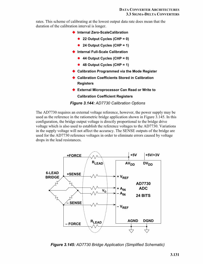
DATA CONVERTER ARCHITECTURES 3.3 SIGMA-DELTA CONVERTERS
3.131
rates. This scheme of calibrating at the lowest output data rate does mean that the duration of the calibration interval is longer.
Figure 3.144: AD7730 Calibration Options The AD7730 requires an external voltage reference, however, the power supply may be used as the reference in the ratiometric bridge application shown in Figure 3.145. In this configuration, the bridge output voltage is directly proportional to the bridge drive voltage which is also used to establish the reference voltages to the AD7730. Variations in the supply voltage will not affect the accuracy. The SENSE outputs of the bridge are used for the AD7730 reference voltages in order to eliminate errors caused by voltage drops in the lead resistances.
Figure 3.145: AD7730 Bridge Application (Simplified Schematic)
Internal Zero-ScaleCalibration
22 Output Cycles (CHP = 0)
24 Output Cycles (CHP = 1)
Internal Full-Scale Calibration
44 Output Cycles (CHP = 0)
48 Output Cycles (CHP = 1)
Calibration Programmed via the Mode Register
Calibration Coefficients Stored in Calibration Registers
External Microprocessor Can Read or Write to
Calibration Coefficient Registers
+5V
AVDD
AGND
+ AIN– AIN
+ VREF
– VREF
RLEAD
RLEAD
6-LEADBRIDGE
AD7730ADC
24 BITS
+SENSE
– SENSE
VO
+FORCE
– FORCE
DVDD
+5V/+3V
DGND
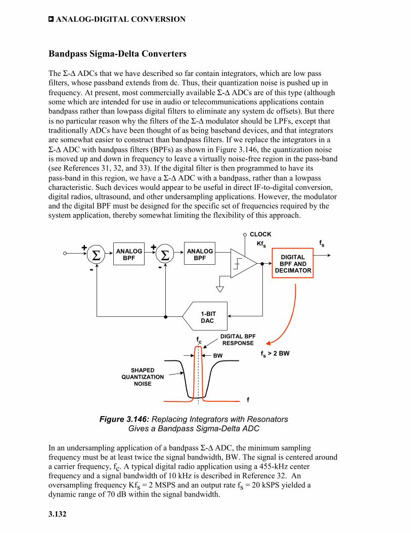
ANALOG-DIGITAL CONVERSION
3.132
Bandpass Sigma-Delta Converters The Σ-∆ ADCs that we have described so far contain integrators, which are low pass filters, whose passband extends from dc. Thus, their quantization noise is pushed up in frequency. At present, most commercially available Σ-∆ ADCs are of this type (although some which are intended for use in audio or telecommunications applications contain bandpass rather than lowpass digital filters to eliminate any system dc offsets). But there is no particular reason why the filters of the Σ-∆ modulator should be LPFs, except that traditionally ADCs have been thought of as being baseband devices, and that integrators are somewhat easier to construct than bandpass filters. If we replace the integrators in a Σ-∆ ADC with bandpass filters (BPFs) as shown in Figure 3.146, the quantization noise is moved up and down in frequency to leave a virtually noise-free region in the pass-band (see References 31, 32, and 33). If the digital filter is then programmed to have its pass-band in this region, we have a Σ-∆ ADC with a bandpass, rather than a lowpass characteristic. Such devices would appear to be useful in direct IF-to-digital conversion, digital radios, ultrasound, and other undersampling applications. However, the modulator and the digital BPF must be designed for the specific set of frequencies required by the system application, thereby somewhat limiting the flexibility of this approach.
Figure 3.146: Replacing Integrators with Resonators
Gives a Bandpass Sigma-Delta ADC In an undersampling application of a bandpass Σ-∆ ADC, the minimum sampling frequency must be at least twice the signal bandwidth, BW. The signal is centered around a carrier frequency, fc. A typical digital radio application using a 455-kHz center frequency and a signal bandwidth of 10 kHz is described in Reference 32. An oversampling frequency Kfs = 2 MSPS and an output rate fs = 20 kSPS yielded a dynamic range of 70 dB within the signal bandwidth.
Σ Σ+
-
+
-
1-BITDAC
ANALOGBPF
ANALOGBPF DIGITAL
BPF ANDDECIMATOR
CLOCK Kfs fs
SHAPEDQUANTIZATION
NOISE
DIGITAL BPFRESPONSEfc
f
BW fs > 2 BW
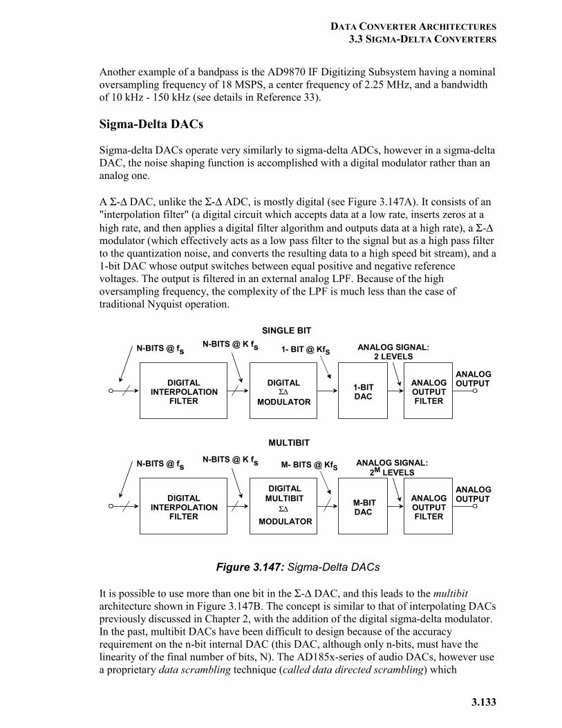
DATA CONVERTER ARCHITECTURES 3.3 SIGMA-DELTA CONVERTERS
3.133
Another example of a bandpass is the AD9870 IF Digitizing Subsystem having a nominal oversampling frequency of 18 MSPS, a center frequency of 2.25 MHz, and a bandwidth of 10 kHz - 150 kHz (see details in Reference 33). Sigma-Delta DACs Sigma-delta DACs operate very similarly to sigma-delta ADCs, however in a sigma-delta DAC, the noise shaping function is accomplished with a digital modulator rather than an analog one. A Σ-∆ DAC, unlike the Σ-∆ ADC, is mostly digital (see Figure 3.147A). It consists of an "interpolation filter" (a digital circuit which accepts data at a low rate, inserts zeros at a high rate, and then applies a digital filter algorithm and outputs data at a high rate), a Σ-∆ modulator (which effectively acts as a low pass filter to the signal but as a high pass filter to the quantization noise, and converts the resulting data to a high speed bit stream), and a 1-bit DAC whose output switches between equal positive and negative reference voltages. The output is filtered in an external analog LPF. Because of the high oversampling frequency, the complexity of the LPF is much less than the case of traditional Nyquist operation.
Figure 3.147: Sigma-Delta DACs It is possible to use more than one bit in the Σ-∆ DAC, and this leads to the multibit architecture shown in Figure 3.147B. The concept is similar to that of interpolating DACs previously discussed in Chapter 2, with the addition of the digital sigma-delta modulator. In the past, multibit DACs have been difficult to design because of the accuracy requirement on the n-bit internal DAC (this DAC, although only n-bits, must have the linearity of the final number of bits, N). The AD185x-series of audio DACs, however use a proprietary data scrambling technique (called data directed scrambling) which
N-BITS @ fsN-BITS @ K fs ANALOG SIGNAL:
2 LEVELS
ANALOGOUTPUTDIGITAL
INTERPOLATIONFILTER
DIGITALΣ∆
MODULATOR
1-BITDAC
ANALOGOUTPUTFILTER
1- BIT @ KfS
N-BITS @ fsN-BITS @ K fs ANALOG SIGNAL:
2M LEVELS
ANALOGOUTPUTDIGITAL
INTERPOLATIONFILTER
DIGITAL
Σ∆
MODULATOR
M-BITDAC
ANALOGOUTPUTFILTER
M- BITS @ KfS
SINGLE BIT
MULTIBIT
MULTIBIT
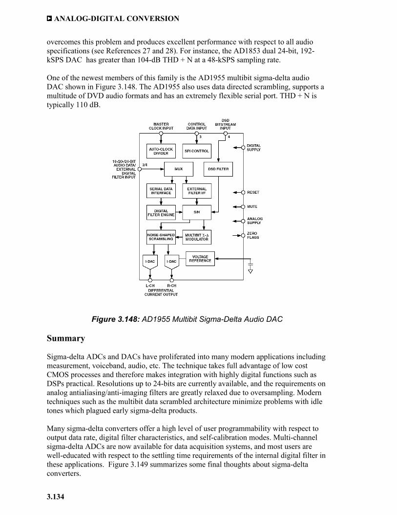
ANALOG-DIGITAL CONVERSION
3.134
overcomes this problem and produces excellent performance with respect to all audio specifications (see References 27 and 28). For instance, the AD1853 dual 24-bit, 192-kSPS DAC has greater than 104-dB THD + N at a 48-kSPS sampling rate. One of the newest members of this family is the AD1955 multibit sigma-delta audio DAC shown in Figure 3.148. The AD1955 also uses data directed scrambling, supports a multitude of DVD audio formats and has an extremely flexible serial port. THD + N is typically 110 dB.
Figure 3.148: AD1955 Multibit Sigma-Delta Audio DAC Summary Sigma-delta ADCs and DACs have proliferated into many modern applications including measurement, voiceband, audio, etc. The technique takes full advantage of low cost CMOS processes and therefore makes integration with highly digital functions such as DSPs practical. Resolutions up to 24-bits are currently available, and the requirements on analog antialiasing/anti-imaging filters are greatly relaxed due to oversampling. Modern techniques such as the multibit data scrambled architecture minimize problems with idle tones which plagued early sigma-delta products. Many sigma-delta converters offer a high level of user programmability with respect to output data rate, digital filter characteristics, and self-calibration modes. Multi-channel sigma-delta ADCs are now available for data acquisition systems, and most users are well-educated with respect to the settling time requirements of the internal digital filter in these applications. Figure 3.149 summarizes some final thoughts about sigma-delta converters.
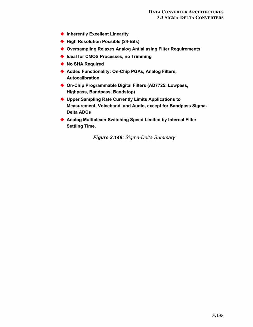
DATA CONVERTER ARCHITECTURES 3.3 SIGMA-DELTA CONVERTERS
3.135
Figure 3.149: Sigma-Delta Summary
Inherently Excellent LinearityHigh Resolution Possible (24-Bits)Oversampling Relaxes Analog Antialiasing Filter RequirementsIdeal for CMOS Processes, no TrimmingNo SHA RequiredAdded Functionality: On-Chip PGAs, Analog Filters, AutocalibrationOn-Chip Programmable Digital Filters (AD7725: Lowpass, Highpass, Bandpass, Bandstop)Upper Sampling Rate Currently Limits Applications to Measurement, Voiceband, and Audio, except for Bandpass Sigma-Delta ADCsAnalog Multiplexer Switching Speed Limited by Internal Filter Settling Time.
ANALOG-DIGITAL CONVERSION
3.136
REFERENCES: 3.3 SIGMA-DELTA CONVERTERS 1. Max W. Hauser, "Principles of Oversampling A/D Conversion," Journal Audio Engineering Society,
Vol. 39, No. 1/2, January/February 1991, pp. 3-26. (one of the best tutorials and practical discussions of the sigma-delta ADC architecture and its history).
2. E. M. Deloraine, S. Van Mierlo, and B. Derjavitch, "Methode et systéme de transmission par
impulsions," French Patent 932,140, issued August, 1946. Also British Patent 627,262, issued 1949. 3. E. M. Deloraine, S. Van Mierlo, and B. Derjavitch, "Communication System Utilizing Constant
Amplitude Pulses of Opposite Polarities," U.S. Patent 2,629,857, filed October 8, 1947, issued February 24, 1953.
4. F. de Jager, "Delta Modulation: A Method of PCM Transmission Using the One Unit Code," Phillips
Research Reports, Vol. 7, 1952, pp. 542-546. (additional work done on delta modulation during the same time period).
5. H. Van de Weg, "Quantizing Noise of a Single Integration Delta Modulation System with an N-Digit
Code," Phillips Research Reports, Vol. 8, 1953, pp. 367-385. (additional work done on delta modulation during the same time period).
6. C. C. Cutler, "Differential Quantization of Communication Signals," U.S. Patent 2,605,361, filed June
29, 1950, issued July 29, 1952. (recognized as the first patent on differential PCM or delta modulation, although actually first invented in the Paris labs of the International Telephone and Telegraph Corporation by E. M. Deloraine, S. Mierlo, and B. Derjavitch a few years earlier)
7. C. C. Cutler, "Transmission Systems Employing Quantization," U.S. Patent 2,927,962, filed April 26,
1954, issued March 8, 1960. (a ground-breaking patent describing oversampling and noise shaping using first and second-order loops to increase effective resolution. The goal was transmission of oversampled noise shaped PCM data without decimation, not a Nyquist-type ADC).
8. C. B. Brahm, "Feedback Integrating System," U.S. Patent 3,192,371, filed September 14, 1961,
issued June 29, 1965. (describes a second-order multibit oversampling noise shaping ADC). 9. H. Inose, Y. Yasuda, and J. Murakami, "A Telemetering System by Code Modulation: ∆-Σ
Modulation," IRE Transactions on Space Electronics Telemetry, Vol. SET-8, September 1962, pp. 204-209. Reprinted in N. S. Jayant, Waveform Quantization and Coding, IEEE Press and John Wiley, 1976, ISBN 0-471-01970-4. (an elaboration on the 1-bit form of Cutler's noise-shaping oversampling concept. This work coined the description of the architecture as 'delta-sigma modulation').
10. H. Inose and Y. Yasuda, "A Unity Bit Coding Method by Negative Feedback," IEEE Proceedings,
Vol. 51, November 1963, pp. 1524-1535. (further discussions on their 1-bit 'delta-sigma' concept). 11. D. J. Goodman, "The Application of Delta Modulation of Analog-to-PCM Encoding," Bell System
Technical Journal, Vol. 48, February 1969, pp. 321-343. Reprinted in N. S. Jayant, Waveform Quantization and Coding, IEEE Press and John Wiley, 1976, ISBN 0-471-01970-4. (the first description of using oversampling and noise shaping techniques followed by digital filtering and decimation to produce a true Nyquist-rate ADC).
12. J. C. Candy, "A Use of Limit Cycle Oscillations to Obtain Robust Analog-to-Digital Converters,"
IEEE Transactions on Communications, Vol. COM-22, December 1974, pp. 298-305. (describes a multibit oversampling noise shaping ADC with output digital filtering and decimation to interpolate between the quantization levels).
13. R. J. van de Plassche, "A Sigma-Delta Modulator as an A/D Converter," IEEE Transactions on
Circuits and Systems, Vol. CAS-25, July 1978, pp. 510-514.
DATA CONVERTER ARCHITECTURES 3.3 SIGMA-DELTA CONVERTERS
3.137
14. B. A. Wooley and J. L. Henry, "An Integrated Per-Channel PCM Encoder Based on Interpolation,"
IEEE Journal of Solid State Circuits, Vol. SC-14, February 1979, pp. 14-20. (one of the first all-integrated CMOS sigma-delta ADCs).
15. B. A. Wooley et al, "An Integrated Interpolative PCM Decoder," IEEE Journal of Solid State
Circuits, Vol. SC-14, February 1979, pp. 20-25. 16. J. C. Candy, B. A. Wooley, and O. J. Benjamin, "A Voiceband Codec with Digital Filtering," IEEE
Transactions on Communications, Vol. COM-29, June 1981, pp. 815-830. 17. J. C. Candy and Gabor C. Temes, Oversampling Delta-Sigma Data Converters, IEEE Press, ISBN
0-87942-258-8, 1992. 18. R. Koch, B. Heise, F. Eckbauer, E. Engelhardt, J. Fisher, and F. Parzefall, "A 12-bit Sigma-Delta
Analog-to-Digital Converter with a 15 MHz Clock Rate," IEEE Journal of Solid-State Circuits, Vol. SC-21, No. 6, December 1986.
19. D. R. Welland, B. P. Del Signore and E. J. Swanson, "A Stereo 16-Bit Delta-Sigma A/D Converter for
Digital Audio," J. Audio Engineering Society, Vol. 37, No. 6, June 1989, pp. 476-485. 20. B. Boser and Bruce Wooley, "The Design of Sigma-Delta Modulation Analog-to-Digital Converters,"
IEEE Journal of Solid-State Circuits, Vol. 23, No. 6, December 1988, pp. 1298-1308. 21. J. Dattorro, A. Charpentier, D. Andreas, "The Implementation of a One-Stage Multirate 64:1 FIR
Decimator for use in One-Bit Sigma-Delta A/D Applications," AES 7th International Conference, May 1989.
22. W.L. Lee and C.G. Sodini, "A Topology for Higher-Order Interpolative Coders," ISCAS PROC.
1987. 23. P.F. Ferguson, Jr., A. Ganesan and R. W. Adams, "One-Bit Higher Order Sigma-Delta A/D
Converters," ISCAS PROC. 1990, Vol. 2, pp. 890-893. 24. Wai Laing Lee, A Novel Higher Order Interpolative Modulator Topology for High Resolution
Oversampling A/D Converters, MIT Masters Thesis, June 1987. 25. R. W. Adams, "Design and Implementation of an Audio 18-Bit Analog-to-Digital Converter Using
Oversampling Techniques," J. Audio Engineering Society, Vol. 34, March 1986, pp. 153-166. 26. P. Ferguson, Jr., A. Ganesan, R. Adams, et. al., "An 18-Bit 20-kHz Dual Sigma-Delta A/D Converter,"
ISSCC Digest of Technical Papers, February 1991. 27. Robert Adams, Khiem Nguyen, and Karl Sweetland, "A 113 dB SNR Oversampling DAC with
Segmented Noise-Shaped Scrambling, " ISSCC Digest of Technical Papers, vol. 41, 1998, pp. 62, 63, 413. (describes a segmented audio DAC with data scrambling).
28. Robert W. Adams and Tom W. Kwan, "Data-directed Scrambler for Multi-bit Noise-shaping D/A
Converters," U.S. Patent 5,404,142, filed August 5, 1993, issued April 4, 1995. (describes a segmented audio DAC with data scrambling).
29. Y. Matsuya, et. al., "A 16-Bit Oversampling A/D Conversion Technology Using Triple-Integration
Noise Shaping," IEEE Journal of Solid-State Circuits, Vol. SC-22, No. 6, December 1987, pp. 921-929.
30. Y. Matsuya, et. al., "A 17-Bit Oversampling D/A Conversion Technology Using Multistage Noise
Shaping," IEEE Journal of Solid-State Circuits, Vol. 24, No. 4, August 1989, pp. 969-975.
ANALOG-DIGITAL CONVERSION
3.138
31. Paul H. Gailus, William J. Turney, and Francis R. Yester, Jr., "Method and Arrangement for a Sigma Delta Converter for Bandpass Signals," U.S. Patent 4,857,928, filed January 28, 1988, issued August 15, 1989.
32. S.A. Jantzi, M. Snelgrove, and P.F. Ferguson Jr., "A 4th-Order Bandpass Sigma-Delta Modulator,"
IEEE Journal of Solid State Circuits, Vol. 38, No. 3, March 1993, pp. 282-291. 33. Paul Hendriks, Richard Schreier, Joe DiPilato, "High Performance Narrowband Receiver Design
Simplified by IF Digitizing Subsystem in LQFP," Analog Dialogue, Vol. 35-3, June-July 2001. available at http://www.analog.com (describes an IF subsystem with a bandpass sigma-delta ADC having a nominal oversampling frequency of 18MSPS, a center frequency of 2.25MHz, and a bandwidth of 10kHz - 150kHz).
DATA CONVERTER ARCHITECTURES 3.3 SIGMA-DELTA CONVERTERS
3.139
General References on Data Conversion and Related Topics 1. Alfred K. Susskind, Notes on Analog-Digital Conversion Techniques, John Wiley, 1957. 2. David F. Hoeschele, Jr., Analog-to-Digital/Digital-to-Analog Conversion Techniques, John Wiley
and Sons, 1968. 3. K. W. Cattermole, Principles of Pulse Code Modulation, American Elsevier Publishing Company,
Inc., 1969, New York NY, ISBN 444-19747-8. 4. Hermann Schmid, Electronic Analog/Digital Conversions, Van Nostrand Reinhold Co., 1970. 5. Dan Sheingold, Analog-Digital Conversion Handbook, First Edition, Analog Devices, 1972. 6. Donald B. Bruck, Data Conversion Handbook, Hybrid Systems Corporation, 1974. 7. Eugene R. Hnatek, A User's Handbook of D/A and A/D Converters, John Wiley, New York, 1976,
ISBN 0-471-40109-9. 8. Nuggehally S. Jayant, Waveform Quantizing and Coding, John Wiley-IEEE Press, 1976, ISBN 0-
87942-074-X. 9. Dan Sheingold, Analog-Digital Conversion Notes, Analog Devices, 1977. 10. C. F. Kurth, editor, IEEE Transactions on Circuits and Systems Special Issue on Analog/Digital
Conversion, CAS-25, No. 7, July 1978. 11. Daniel J. Dooley, Data Conversion Integrated Circuits, John Wiley-IEEE Press, 1980, ISBN 0-471-
08155-8. 12. Bernard M. Gordon, The Analogic Data-Conversion Systems Digest, Fourth Edition, Analogic
Corporation, 1981. 13. Eugene L. Zuch, Data Acquisition and Conversion Handbook, Datel-Intersil, 1982. 14. Frank F. E. Owen, PCM and Digital Transmission Systems, McGraw-Hill, 1982, ISBN 0-07-
047954-2. 15. Dan Sheingold, Analog-Digital Conversion Handbook, Analog Devices/Prentice-Hall, 1986, ISBN
0-13-032848-0. 16. Matthew Mahoney, DSP-Based Testing of Analog and Mixed-Signal Circuits, IEEE Computer
Society Press, 1987, ISBN 0-8186-0785-8. 17. Michael J. Demler, High-Speed Analog-to-Digital Conversion, Academic Press, Inc., 1991, ISBN 0-
12-209048-9. 18. J. C. Candy and Gabor C. Temes, Oversampling Delta-Sigma Data Converters, IEEE Press, ISBN
0-87942-258-8, 1992. 19. David F. Hoeschele, Jr., Analog-to-Digital and Digital-to-Analog Conversion Techniques, Second
Edition, John Wiley and Sons, 1994, ISBN-0-471-57147-4. 20. Rudy van de Plassche, Integrated Analog-to-Digital and Digital-to-Analog Converters, Kluwer
Academic Publishers, 1994, ISBN 0-7923-9436-4. 21. David A. Johns and Ken Martin, Analog Integrated Circuit Design, John Wiley, 1997, ISBN 0-471-
14448-7.
ANALOG-DIGITAL CONVERSION
3.140
22. Mikael Gustavsson, J. Jacob Wikner, and Nianxiong Nick Tan, CMOS Data Converters for
Communications, Kluwer Academic Publishers, 2000, ISBN 0-7923-7780-X. 23. R. Jacob Baker, CMOS Circuit Design Volumes I and II, John Wiley-IEEE Computer Society, 2002,
ISBN 0-4712-7256-6. 24. Rudy van de Plassche, CMOS Integrated Analog-to-Digital and Digital-to-Analog Converters,
Second Edition, Kluwer Academic Publishers, 2003, ISBN 1-4020-7500-6. Analog Devices' Seminar Series: 25. Walt Kester, Practical Analog Design Techniques, Analog Devices, 1995, ISBN 0-916550-16-8,
available for download at http://www.analog.com. 26. Walt Kester, High Speed Design Techniques, Analog Devices, 1996, ISBN 0-916550-17-6, available
for download at http://www.analog.com. 27. Walt Kester, Practical Design Techniques for Power and Thermal Management, Analog Devices,
1998, ISBN 0-916550-19-2, available for download at http://www.analog.com. 28. Walt Kester, Practical Design Techniques for Sensor Signal Conditioning, Analog Devices, 1999,
ISBN 0-916550-20-6, available for download at http://www.analog.com. 29. Walt Kester, Mixed-Signal and DSP Design Techniques, Analog Devices, 2000, ISBN 0-916550-22-
2, available for download at http://www.analog.com. 30. Walt Kester, Mixed-Signal and DSP Design Techniques, Analog Devices and Newnes (An Imprint
of Elsevier Science), ISBN 0-75067-611-6, 2003. 31. Walter G. Jung, Op Amp Applications, Analog Devices, 2002, ISBN 0-916550-26-5.