Embed Size (px)
Citation preview
3296 IEEE TRANSACTIONS ON INDUSTRIAL ELECTRONICS, VOL. 62, NO. 5, MAY 2015
DC–DC Converter for Dual-Voltage AutomotiveSystems Based on Bidirectional Hybrid
Switched-Capacitor ArchitecturesDaniel Flores Cortez, Gierri Waltrich, Student Member, IEEE , Joseph Fraigneaud,
Harmonie Miranda, and Ivo Barbi, Fellow, IEEE
Abstract—Automotive embedded electronic systemshave been increasing in power and complexity and, there-fore, more advanced power electronic converters are nec-essary in these vehicles. Several dual-voltage (42 V/14 V)bidirectional converter architectures have been proposedfor automotive systems in recent years. However, most ofthem have low efficiency or are based in series and parallelconfigurations with large number of semiconductors andmagnetics devices. Therefore, in this paper, we propose abidirectional high-efficiency converter with lower numberof components. This converter was created by merging aswitched-capacitor converter and a conventional bidirec-tional converter, resulting in a hybrid topology. The voltageacross the semiconductors of the proposed converter isequal to half of the highest voltage source value. Further-more, the topology is composed of only one inductor tocontrol the power flow between the two voltage sources.To verify all the mentioned features, a prototype was im-plemented experimentally, reaching a maximum efficiencyof 97.5%.
Index Terms—Bidirectional, dc–dc, hybrid, switched-capacitor (SC).
I. INTRODUCTION
THE AUTOMOTIVE industry has benefited from perma-nent technological advances that have been increasing
the need for more advanced power electronics devices. Whileelectric loads on vehicles are nowadays set around 2 kW, inthe next few years, the electric power consumed may overcome5 kW [1] for internal combustion engine vehicles and 40 kWfor fully electric vehicles [2]. This increase in energy demandis due to the massive use of electronic systems, which allowsmore comfort and flexibility. Thus, it will be unviable to main-tain the 14 V in automotive systems, due to the high currentlevels through the electronic devices. Therefore, 42-V systemshave been increasingly used in automotive applications. Studiesshow the benefits of using a 42-V system in vehicles [3]. Some
Manuscript received February 18, 2014; revised May 22, 2014; ac-cepted July 14, 2014. Date of publication August 21, 2014; date ofcurrent version April 8, 2015. This work was supported by the FederalUniversity of Santa Catarina and the Instituto de Eletrônica de Potência.
D. Flores Cortez, G. Waltrich, and I. Barbi are with the Depart-ment of Electrical Engineering, Federal University of Santa Catarina,Florianopolis 88040-900, Brazil (e-mail: [email protected]).
J. Fraigneaud and H. Miranda are with the Ecole Navale, 29240 Brest,France.
Color versions of one or more of the figures in this paper are availableonline at http://ieeexplore.ieee.org.
Digital Object Identifier 10.1109/TIE.2014.2350454
Fig. 1. DC–DC converter for 42-/14-V systems for automotive applica-tions [1].
of these benefits are the improvement of electronics efficiencyand, consequently, lower losses.
Nevertheless, many electronics devices such as lamps,switches or fuses still use 14-V systems [4], and therefore,it will be very expensive to completely abandon this system.Thus, a dc–dc converter could be used to supply energy for both14- and 42-V devices, as shown in Fig. 1. In this configuration,the 42-V bus will supply high-power loads, whereas the 14-Vbus will provide energy for the low-power components.
Several dual-voltage converter architectures have been pro-posed in recent years [1]. A conventional solution to designingthe electronic interface for a dual-voltage system is a bilateraldc–dc converter. This topology is composed of a buck and aboost converter separated in two different stages sharing thesame magnetic core [1]. As an advantage, this topology has lownumber of components. However, when it is designed for high-power applications (>1 kW), it requires high-voltage and high-current semiconductors. This topology also has lower efficiencyfor such power levels.
In order to increase the efficiency of the dual-voltage dc–dcconverters, alternative solutions have been proposed [4]–[12].Most of these solutions are based in series and parallelconfigurations. These converters have higher efficiencies andlower stress in the semiconductors compared with conventionaltopologies. However, these structures have large number ofsemiconductors and magnetics. For instance, in [4], a bidirec-tional converter is proposed using switch capacitor cells to con-nect two voltage sources applied in a dual-voltage automotivesystem. This topology has lower voltage stress; however, it has alarge number of components. Furthermore, this topology cannotcontrol the power flow between the two voltage sources becauseit operates with fixed duty cycle.
In recent years switched-capacitor (SC) converters have be-come an attractive solution for dc–dc converters with high staticgain, as shown in [16]–[24]. Recently, the same idea has beenapplied in ac–ac [25], [26] and dc–ac [27] converters design.
0278-0046 © 2014 IEEE. Personal use is permitted, but republication/redistribution requires IEEE permission.See http://www.ieee.org/publications_standards/publications/rights/index.html for more information.
FLORES CORTEZ et al.: DC–DC CONVERTER FOR AUTOMOTIVE SYSTEMS BASED ON SC ARCHITECTURES 3297
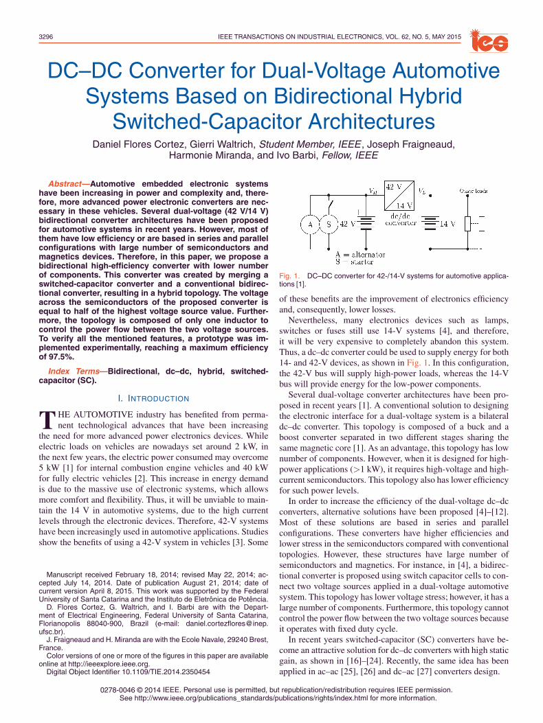
Fig. 2. Proposed bidirectional hybrid SC converter.
Since SC converters do not have magnetic elements, it ispossible to obtain converters with high efficiency, small size,light weight, reduced electromagnetic interference problems,and small output ripple [28], [29]. Furthermore, these convert-ers can be easily implemented in integrated circuits [31], [32]and, consequently, increase their power density and efficiency.Another benefit of this structure is the low blocking voltagestress across all the semiconductors. Furthermore, the SC con-verter analysis can be represented by an equivalent circuits, asdescribed in [17]–[21], becoming its analysis simpler.
If an inductor is placed in a SC structure, it is possible to cre-ate a hybrid solution [13]–[15]. This hybrid solution topologyis composed of a conventional dc–dc boost converter connectedto diode-capacitors cells multiplier at the output. Therefore,the static gain of this converter might be doubled, keeping thesame voltage level (VH/2) across all the switches. Anotheradvantage is the possibility of adding more capacitors modulesat the output, increasing even more the static gain, preservingthe same low voltage across the switches. However, the hybridtopology shown in [13] and [14] does not allow bidirectionalpower flow. Therefore, in this paper, a bidirectional hybridSC converter is proposed, as shown in Fig. 2. The proposedconverter preserves the advantages of the topology shown in[13] and [14], and it adds the benefit of bidirectional power flowcontrol. Furthermore, at the low voltage and the high currentside, due to the presence of the high-frequency inductor L, thecurrent ripple is low, in opposition to the voltage-fed circuits,previously reported in the scientific literature.
To validate all the mentioned characteristics, a 140-W pro-totype was implemented experimentally, reaching a maximumefficiency of 97.5%.
II. THEORETICAL ANALYSIS OF
THE PROPOSED TOPOLOGY
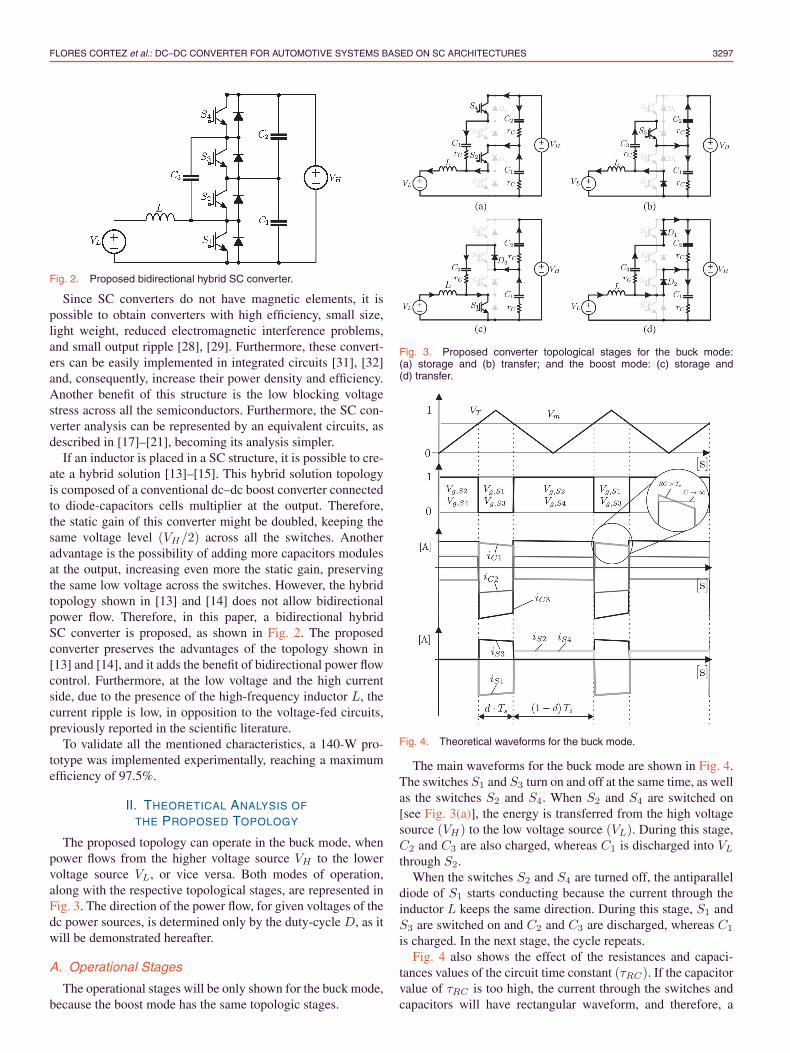
The proposed topology can operate in the buck mode, whenpower flows from the higher voltage source VH to the lowervoltage source VL, or vice versa. Both modes of operation,along with the respective topological stages, are represented inFig. 3. The direction of the power flow, for given voltages of thedc power sources, is determined only by the duty-cycle D, as itwill be demonstrated hereafter.
A. Operational Stages
The operational stages will be only shown for the buck mode,because the boost mode has the same topologic stages.
Fig. 3. Proposed converter topological stages for the buck mode:(a) storage and (b) transfer; and the boost mode: (c) storage and(d) transfer.
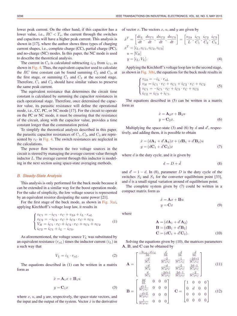
Fig. 4. Theoretical waveforms for the buck mode.
The main waveforms for the buck mode are shown in Fig. 4.The switches S1 and S3 turn on and off at the same time, as wellas the switches S2 and S4. When S2 and S4 are switched on[see Fig. 3(a)], the energy is transferred from the high voltagesource (VH) to the low voltage source (VL). During this stage,C2 and C3 are also charged, whereas C1 is discharged into VL
through S2.When the switches S2 and S4 are turned off, the antiparallel
diode of S1 starts conducting because the current through theinductor L keeps the same direction. During this stage, S1 andS3 are switched on and C2 and C3 are discharged, whereas C1
is charged. In the next stage, the cycle repeats.Fig. 4 also shows the effect of the resistances and capaci-
tances values of the circuit time constant (τRC). If the capacitorvalue of τRC is too high, the current through the switches andcapacitors will have rectangular waveform, and therefore, a
3298 IEEE TRANSACTIONS ON INDUSTRIAL ELECTRONICS, VOL. 62, NO. 5, MAY 2015
lower peak current. On the other hand, if this capacitor has alower value, i.e., RC < Ts, the current through the switchesand capacitors will have a higher peak current. This analysis isshown in [17], where the author shows three types of chargingcurrent shapes, i.e., complete charge (CC), partial charge (PC),and no-charge (NC) modes. In this paper, the NC mode is usedto describe the theoretical analysis.
The current in C3 is calculated subtracting iC2 from iC1, asshown in Fig. 4. Thus, the equivalent capacitor used to calculatethe RC time constant can be found summing C2 and C3, atthe first stage, or summing C1 and C3 at the second stage.Therefore, C1 and C2 should have similar values to preservethe same peak current.
The equivalent resistance that determines the circuit timeconstant is calculated by summing the capacitor resistances ineach operational stage. Therefore, once determined the capac-itor value, its parasitic resistance will define the operationalmode, i.e., CC, PC, or NC mode [17]. For the circuit to operateon the PC or NC mode, it must be ensuring that the resistanceof the circuit, along with the capacitor value, provides a timeconstant longer than the commutation period.
To simplify the theoretical analysis described in this paper,the parasitic capacitor resistances of C1, C2, and C3 are repre-sented by rC in Fig. 4. The switch resistances are neglected inthe calculations.
The power flow between the two voltage sources in thecircuit is steered by managing the average current value throughinductor L. The average current through this inductor is model-ing in the next section using space-state averaging methods.
B. Steady-State Analysis
This analysis is only performed for the buck mode because itcan be extended in a similar way for the boost operation mode.For the sake of simplicity, the low voltage source is representedby an equivalent resistor dissipating the same power [21].
For the first stage of the buck mode, as shown in Fig. 3(a),applying Kirchhoff’s voltage loop law, it results in
⎧⎪⎨⎪⎩
vC1 = −iC1 · rC + vLb + iL · roLvC2 = −iC2 · rC + iC3 · rC + vC3
VH = iC1 · rC + iC2 · rC + vC1 + vC2
iC2 = iC1 + iL − iC3.
(1)
As aforementioned, the voltage source VL was substituted byan equivalent resistance (roL) times the inductor current (iL) ina such way that
VL = iL · roL. (2)
The equations described in (1) can be written in a matrixform as
x =A1x+B1u
y =C1x (3)
where x, u, and y are, respectively, the space-state vectors, andthe input and the output of the system. Vector x is the derivative
of vector x. The vectors x, u, and y are given by
xT =
[diLdt
,dvC1
dt,dvC2
dt,dvC3
dt
]=
[vLb
L,iC1
C1,iC2
C2,iC3
C3
]
xT = [iL, vC1, vC2, vC3]
u = [VH ]
y = [iL, VL]. (4)
Applying the Kirchhoff’s voltage loop law to the second stage,as shown in Fig. 3(b), the equations for the buck mode results in⎧⎪⎨
⎪⎩vLb = −iL · roLvH = iC1 · rC + vC1 + iC2 · rC + vC2
vC1 = −iC1 · rC + iC3 · rC + vC3
iC2 = iC3 + iC1.
(5)
The equations described in (5) can be written in a matrixform as
x =A2x+B2u
y =C2x. (6)
Multiplying the space-state (3) and (6) by d and d′, respec-tively, and adding them, it is possible to obtain
x =(dA1 + d′A2)x+ (dB1 + d′B2)u
y =(dC1 + d′C2)x (7)
where d is the duty cycle, and it is given by
d = D + d (8)
and d′ = 1− d. In (8), parameter D is the duty cycle of theswitches S2 and S4 for the converter equilibrium point [33],and d is a small signal variation around of equilibrium point.
The complete system given by (7) could be written in acompact matrix form as
x =Ax+Bu
y =Cx (9)
where
A =(dA1 + d′A2)
B =(dB1 + d′B2)
C =(dC1 + d′C2). (10)
Solving the equations given by (10), the matrices parametersA, B, and C can be obtained by
A =
⎡⎢⎢⎢⎢⎣
−3roL−d·rC3L
d3L
−d3L
−d3L
−d3C1
−23C1rC
−13C1rC
−2d+13C1rC
−d3C2
−d3C2rC
−23C2rC
2d−13C2rC
d3C3
−2d+13C3rC
2d−13C3rC
−23C3rC
⎤⎥⎥⎥⎥⎦ (11)
B =
⎡⎢⎢⎢⎢⎣
2d3L 0 0 0d+1
3C1rC0 0 0
−d+23C2rC
0 0 0
13C3rC
0 0 0
⎤⎥⎥⎥⎥⎦ C =
⎡⎢⎢⎢⎣1 0 0 0
0 d 0 0
0 0 0 0
0 0 0 0
⎤⎥⎥⎥⎦ (12)
FLORES CORTEZ et al.: DC–DC CONVERTER FOR AUTOMOTIVE SYSTEMS BASED ON SC ARCHITECTURES 3299
where roL in (11) is the equivalent resistance, which representsthe low voltage source (VL). This equivalent resistance can becalculated by
roL =V 2L
P(13)
where P is the output power converter. To simplify the calcula-tions, the input and the output powers are considered the same.
For steady-state analysis, the derivative of the space-statevector is zero (x = 0); thus, x = A−1 +Bu. Therefore, theanalytical solution for x is given by
x =
⎡⎢⎣
iLvC1
vC2
vC3
⎤⎥⎦ =
⎡⎢⎢⎢⎢⎢⎢⎣
−4d(1−d)VH
3d·rC+8roL−8d·roL
− (d2rC−d·rC−4roL+4d·roL)VH
3d·rC+8roL−8d·roL(d2rC+2d·rC+4roL−4d·roL)VH
3d·rC+8roL−8d·roL(2d2rC+d·rC−4roL+4d·roL)VH
3d·rC+8roL−8d·roL
⎤⎥⎥⎥⎥⎥⎥⎦. (14)
Solving (14), the ideal static gain of the proposed convertercan be determined by
GrC→0
=VL
VH=
D
2. (15)
To calculate (15), the capacitor resistance (rC) in (14) wasconsidered null.
The static gain considering the nonidealities of the capaci-tors, i.e., rC �= 0 is given by
G =D · (vc1 + iC1 · rC)
VH=
4DroL(1−D)
3Drc + 8roL − 8DroL. (16)
Rewriting (13) as
roL =G · VH
iL(17)
and substituting (17) into (16), the static gain becomes
G = − 4D ·G · VH(1−D)
−3rciLD − 8G · VH + 8D ·G · VH, or (18)
G = −D
⌊38rCiLVH
− 12 (1−D)
⌋(1−D)
. (19)
Supposing
IL =8
3
VH
rC(20)
the static gain can be rewritten as
G = −D
⌊iLIL
− 12 (1−D)
⌋(1−D)
(21)
where IL represents the normalized inductor current. Thus, theinductor current iL can be determined by
iL =(1−D)
D
(D
2−G
)IL. (22)
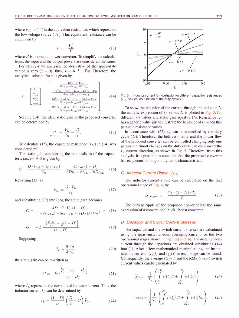
Fig. 5. Inductor current (iL) behavior for different capacitor resistances(rC) values, as function of the duty cycle D.
To show the behavior of the current through the inductor L,the analytic expression of iL versus D is plotted in Fig. 5, fordifferent rC values and static gain equal to 1/3. Resistance rChas a generic value just to illustrate the behavior of iL when thisparasitic resistance varies.
In accordance with (22), iL can be controlled by the dutycycle (D). Therefore, the bidirectionality and the power flowof the proposed converter can be controlled changing only oneparameter. Small changes on the duty cycle can even invert theiL current direction, as shown in Fig. 5. Therefore, from thisanalysis, it is possible to conclude that the proposed converterhas easy control and good dynamic characteristics.
C. Inductor Current Ripple (ΔiL)
The inductor current ripple can be calculated on the firstoperational stage of Fig. 4, by
ΔiL,pk−pk =VL · (1−D) · Ts
L. (23)
The current ripple of the proposed converter has the sameexpression of a conventional buck+boost converter.
D. Capacitor and Switch Current Stresses
The capacitor and the switch current stresses are calculatedusing the quasi-instantaneous averaging current for the twooperational stages shown in Fig. 3(a) and (b). The instantaneouscurrent through the capacitors are obtained substituting (14)into (1). After a few mathematical manipulations, the instan-taneous currents (i1(t) and i2(t)) in each stage can be found.Consequently, the average (〈i〉Ts) and the RMS (iRMS) switchcurrent values can be calculated by
〈i〉Ts =1
Ts
⎛⎝
dTs∫0
i1(t)dt+
Ts∫dTs
i2(t)dt
⎞⎠ (24)
iRMS =
√√√√√ 1
Ts
⎛⎝
dTs∫0
i1(t)2dt+
Ts∫dTs
i2(t)2dt
⎞⎠. (25)
3300 IEEE TRANSACTIONS ON INDUSTRIAL ELECTRONICS, VOL. 62, NO. 5, MAY 2015
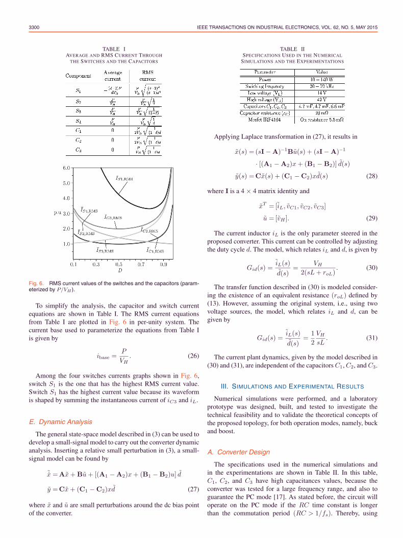
TABLE IAVERAGE AND RMS CURRENT THROUGH
THE SWITCHES AND THE CAPACITORS
Fig. 6. RMS current values of the switches and the capacitors (param-eterized by P/VH ).
To simplify the analysis, the capacitor and switch currentequations are shown in Table I. The RMS current equationsfrom Table I are plotted in Fig. 6 in per-unity system. Thecurrent base used to parameterize the equations from Table Iis given by
ibase =P
VH. (26)
Among the four switches currents graphs shown in Fig. 6,switch S1 is the one that has the highest RMS current value.Switch S1 has the highest current value because its waveformis shaped by summing the instantaneous current of iC3 and iL.
E. Dynamic Analysis
The general state-space model described in (3) can be used todevelop a small-signal model to carry out the converter dynamicanalysis. Inserting a relative small perturbation in (3), a small-signal model can be found by
˜x =Ax+Bu+ [(A1 −A2)x+ (B1 −B2)u] d
y =Cx+ (C1 −C2)xd (27)
where x and u are small perturbations around the dc bias pointof the converter.
TABLE IISPECIFICATIONS USED IN THE NUMERICAL
SIMULATIONS AND THE EXPERIMENTATIONS
Applying Laplace transformation in (27), it results in
x(s) = (sI−A)−1Bu(s) + (sI−A)−1
· [(A1 −A2)x+ (B1 −B2)] d(s)
y(s) =Cx(s) + (C1 −C2)xd(s) (28)
where I is a 4 × 4 matrix identity and
xT = [iL, vC1, vC2, vC3]
u = [vH ]. (29)
The current inductor iL is the only parameter steered in theproposed converter. This current can be controlled by adjustingthe duty cycle d. The model, which relates iL and d, is given by
Gid(s) =iL(s)
d(s)=
VH
2(sL+ roL). (30)
The transfer function described in (30) is modeled consider-ing the existence of an equivalent resistance (roL) defined by(13). However, assuming the original system, i.e., using twovoltage sources, the model, which relates iL and d, can begiven by
Gid(s) =iL(s)
d(s)=
1
2
VH
sL. (31)
The current plant dynamics, given by the model described in(30) and (31), are independent of the capacitors C1, C2, and C3.
III. SIMULATIONS AND EXPERIMENTAL RESULTS
Numerical simulations were performed, and a laboratoryprototype was designed, built, and tested to investigate thetechnical feasibility and to validate the theoretical concepts ofthe proposed topology, for both operation modes, namely, buckand boost.
A. Converter Design
The specifications used in the numerical simulations andin the experimentations are shown in Table II. In this table,C1, C2, and C3 have high capacitances values, because theconverter was tested for a large frequency range, and also toguarantee the PC mode [17]. As stated before, the circuit willoperate on the PC mode if the RC time constant is longerthan the commutation period (RC > 1/fs). Thereby, using
FLORES CORTEZ et al.: DC–DC CONVERTER FOR AUTOMOTIVE SYSTEMS BASED ON SC ARCHITECTURES 3301
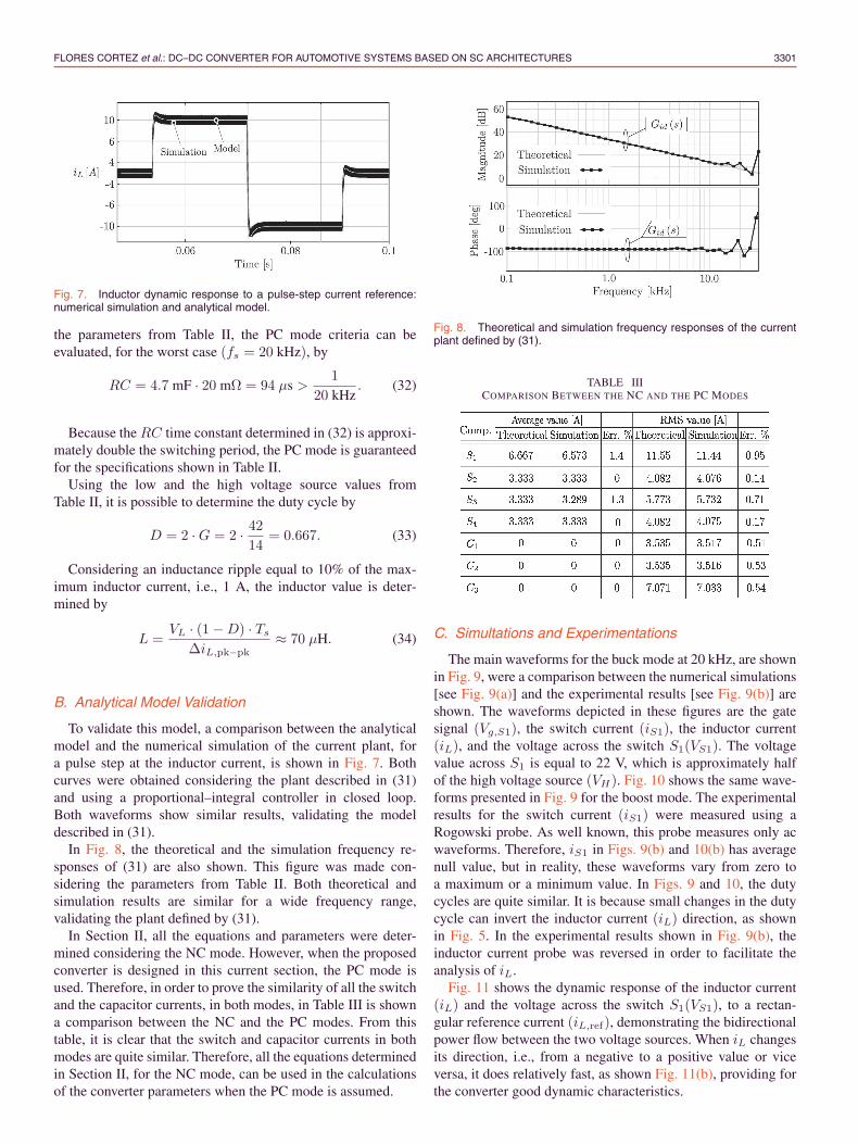
Fig. 7. Inductor dynamic response to a pulse-step current reference:numerical simulation and analytical model.
the parameters from Table II, the PC mode criteria can beevaluated, for the worst case (fs = 20 kHz), by
RC = 4.7 mF · 20 mΩ = 94 μs >1
20 kHz. (32)
Because the RC time constant determined in (32) is approxi-mately double the switching period, the PC mode is guaranteedfor the specifications shown in Table II.
Using the low and the high voltage source values fromTable II, it is possible to determine the duty cycle by
D = 2 ·G = 2 · 4214
= 0.667. (33)
Considering an inductance ripple equal to 10% of the max-imum inductor current, i.e., 1 A, the inductor value is deter-mined by
L =VL · (1−D) · Ts
ΔiL,pk−pk≈ 70 μH. (34)
B. Analytical Model Validation
To validate this model, a comparison between the analyticalmodel and the numerical simulation of the current plant, fora pulse step at the inductor current, is shown in Fig. 7. Bothcurves were obtained considering the plant described in (31)and using a proportional–integral controller in closed loop.Both waveforms show similar results, validating the modeldescribed in (31).
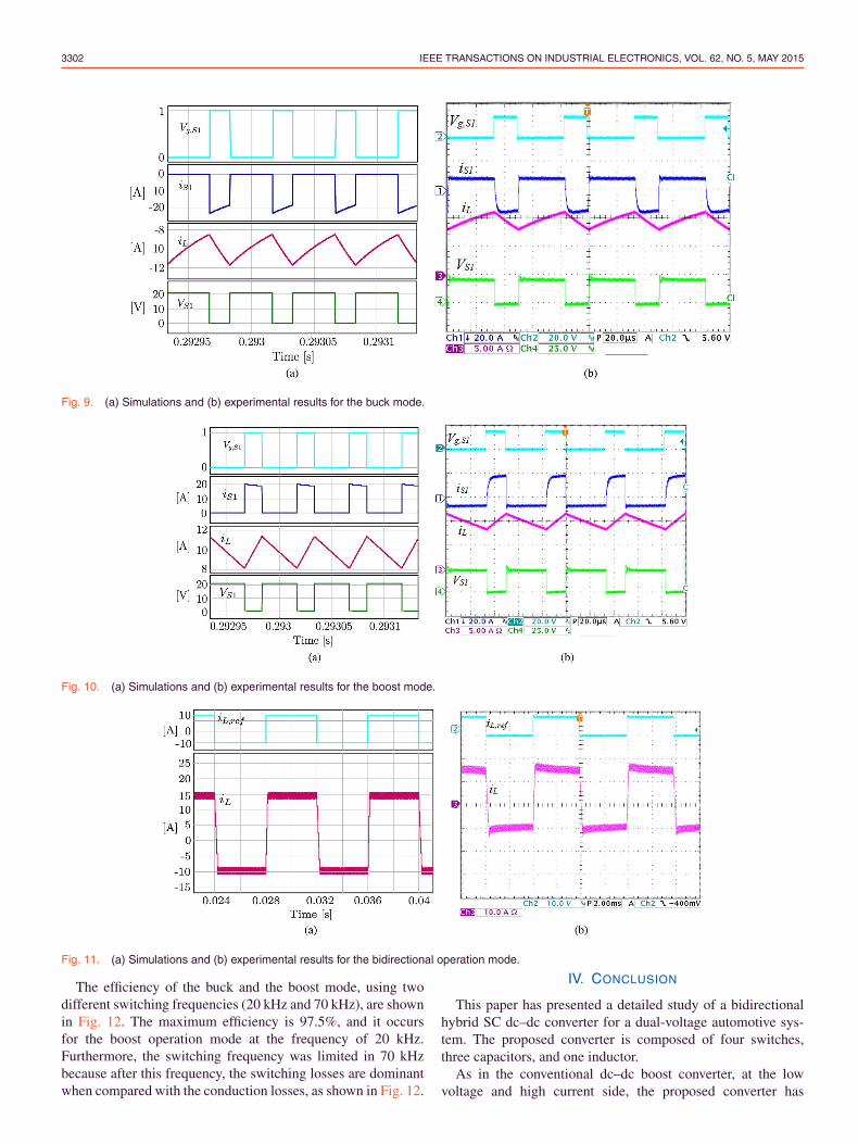
In Fig. 8, the theoretical and the simulation frequency re-sponses of (31) are also shown. This figure was made con-sidering the parameters from Table II. Both theoretical andsimulation results are similar for a wide frequency range,validating the plant defined by (31).
In Section II, all the equations and parameters were deter-mined considering the NC mode. However, when the proposedconverter is designed in this current section, the PC mode isused. Therefore, in order to prove the similarity of all the switchand the capacitor currents, in both modes, in Table III is showna comparison between the NC and the PC modes. From thistable, it is clear that the switch and capacitor currents in bothmodes are quite similar. Therefore, all the equations determinedin Section II, for the NC mode, can be used in the calculationsof the converter parameters when the PC mode is assumed.
Fig. 8. Theoretical and simulation frequency responses of the currentplant defined by (31).
TABLE IIICOMPARISON BETWEEN THE NC AND THE PC MODES
C. Simultations and Experimentations
The main waveforms for the buck mode at 20 kHz, are shownin Fig. 9, were a comparison between the numerical simulations[see Fig. 9(a)] and the experimental results [see Fig. 9(b)] areshown. The waveforms depicted in these figures are the gatesignal (Vg,S1), the switch current (iS1), the inductor current(iL), and the voltage across the switch S1(VS1). The voltagevalue across S1 is equal to 22 V, which is approximately halfof the high voltage source (VH). Fig. 10 shows the same wave-forms presented in Fig. 9 for the boost mode. The experimentalresults for the switch current (iS1) were measured using aRogowski probe. As well known, this probe measures only acwaveforms. Therefore, iS1 in Figs. 9(b) and 10(b) has averagenull value, but in reality, these waveforms vary from zero toa maximum or a minimum value. In Figs. 9 and 10, the dutycycles are quite similar. It is because small changes in the dutycycle can invert the inductor current (iL) direction, as shownin Fig. 5. In the experimental results shown in Fig. 9(b), theinductor current probe was reversed in order to facilitate theanalysis of iL.
Fig. 11 shows the dynamic response of the inductor current(iL) and the voltage across the switch S1(VS1), to a rectan-gular reference current (iL,ref), demonstrating the bidirectionalpower flow between the two voltage sources. When iL changesits direction, i.e., from a negative to a positive value or viceversa, it does relatively fast, as shown Fig. 11(b), providing forthe converter good dynamic characteristics.
3302 IEEE TRANSACTIONS ON INDUSTRIAL ELECTRONICS, VOL. 62, NO. 5, MAY 2015
Fig. 9. (a) Simulations and (b) experimental results for the buck mode.
Fig. 10. (a) Simulations and (b) experimental results for the boost mode.
Fig. 11. (a) Simulations and (b) experimental results for the bidirectional operation mode.
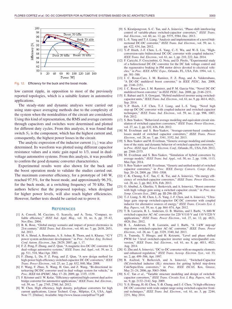
The efficiency of the buck and the boost mode, using twodifferent switching frequencies (20 kHz and 70 kHz), are shownin Fig. 12. The maximum efficiency is 97.5%, and it occursfor the boost operation mode at the frequency of 20 kHz.Furthermore, the switching frequency was limited in 70 kHzbecause after this frequency, the switching losses are dominantwhen compared with the conduction losses, as shown in Fig. 12.
IV. CONCLUSION
This paper has presented a detailed study of a bidirectionalhybrid SC dc–dc converter for a dual-voltage automotive sys-tem. The proposed converter is composed of four switches,three capacitors, and one inductor.
As in the conventional dc–dc boost converter, at the lowvoltage and high current side, the proposed converter has
FLORES CORTEZ et al.: DC–DC CONVERTER FOR AUTOMOTIVE SYSTEMS BASED ON SC ARCHITECTURES 3303
Fig. 12. Efficiency for the buck and the boost mode.
low current ripple, in opposition to most of the previouslyreported topologies, which is a suitable feature in automotiveapplications.
The steady-state and dynamic analyses were carried outusing state-space averaging methods due to the complexity ofthe system when the nonidealities of the circuit are considered.Using this kind of representation, the RMS and average currentsthrough capacitors and switches were determined and plottedfor different duty cycles. From this analysis, it was found thatswitch S1 is the component, which has the highest current and,consequently, the highest power losses in the circuit.
The analytic expression of the inductor current (iL) was alsodetermined. Its waveform was plotted using different capacitorresistance values and a static gain equal to 1/3, usual in dual-voltage automotive systems. From this analysis, it was possibleto confirm the good dynamic converter characteristics.
Experimental results were also shown for the buck andthe boost operation mode to validate the studies carried out.The maximum converter efficiency, for a prototype of 140 W,reached 97.5%, for the boost mode, and approximately 96.3%,for the buck mode, at a switching frequency of 70 kHz. Theauthors believe that the proposed topology, when designedfor higher power levels, will also reach higher efficiencies.However, further tests should be carried out to prove it.
REFERENCES
[1] A. Consoli, M. Cacciato, G. Scarcely, and A. Testa, “Compact, re-liable efficiency,” IEEE Ind. Appl. Mag., vol. 10, no. 6, pp. 35–42,Nov./Dec. 2004.
[2] B. K. Bose, “Global energy scenario and impact of power electronics in21st century,” IEEE Trans. Ind. Electron., vol. 60, no. 7, pp. 2638, 2651,Jul. 2013.
[3] M. A. Shrud, A. Bousbaine, A. S. Ashur, R. Thorn, and A. Kharaz, “42 Vpower system architecture development,” in Proc. 3rd Inst. Eng. Technol.Conf. Autom. Electron., Jun. 28/29, 2007, pp. 1, 17.
[4] F. Z. Peng, F. Zhang, and Z. Qian, “A magnetic-less DC-DC converter fordual-voltage automotive systems,” IEEE Trans. Ind. Appl., vol. 39, no. 2,pp. 511, 518, Mar./Apr. 2003.
[5] F. Zhang, L. Du, F. Z. Peng, and Z. Qian, “A new design method forhigh-power high-efficiency switched-capacitor DC-DC converters,” IEEETrans. Power Electron., vol. 23, no. 2, pp. 832, 840, Mar. 2008.
[6] F. Wang, F. Zhuo, X. Wang, H. Guo, and Z. Wang, “Bi-directional in-terleaving DC/DC converter used in dual voltage system for vehicle,” inProc. IEEE 6th IPEMC, May 17–20, 2009, pp. 1335, 1339.
[7] F. Krismer and J. W. Kolar, “Efficiency-optimized high-current dual activebridge converter for automotive applications,” IEEE Trans. Ind. Electron.,vol. 59, no. 7, pp. 2745, 2760, Jul. 2012.
[8] W. Chen, High efficiency, high density, polyphase converters for highcurrent applications, Linear Technol. Corp., Milpitas, CA, USA, Appl.Note 77. [Online]. Available: http://www.linear.com/pdf/an77f.pdf
[9] S. Kiratipongvoot, S.-C. Tan, and A. Ioinovici, “Phase-shift interleavingcontrol of variable-phase switched-capacitor converters,” IEEE Trans.Ind. Electron., vol. 60, no. 12, pp. 5575, 5584, Dec. 2013.
[10] L.-S. Yang and T.-J. Liang, “Analysis and implementation of a novel bidi-rectional DC-DC converter,” IEEE Trans. Ind. Electron., vol. 59, no. 1,pp. 422, 434, Jan. 2012.
[11] Y.-P. Hsieh, J.-F. Chen, L.-S. Yang, C.-Y. Wu, and W.-S. Liu, “High-conversion-ratio bidirectional DC-DC converter with coupled inductor,”IEEE Trans. Ind. Electron., vol. 61, no. 1, pp. 210, 222, Jan. 2014.
[12] F. Caricchi, F. Crescimbini, G. Noia, and D. Pirolo, “Experimental studyof a bidirectional DC-DC converter for the DC link voltage control andthe regenerative braking in PM motor drives devoted to electrical vehi-cles,” in Proc. IEEE APEC Expo., Orlando, FL, USA, Feb. 1994, vol. 1,pp. 381–386.
[13] J. C. Rosas-Caro, J. M. Ramirez, F. Z. Peng, and A. Valderrabano,“A DC–DC multilevel boost converter,” in IEEE PESC, Jun. 2008,pp. 2146–2151.
[14] J. C. Rosas-Caro, J. M. Ramirez, and P. M. Garcia-Vite, “Novel DC-DCmultilevel boost converter,” in IEEE PESC, Jun. 2008, pp. 2146–2151.
[15] E. Babaei and S. S. Gowgani, “Hybrid multilevel inverter using switched-capacitor units,” IEEE Trans. Ind. Electron., vol. 61, no. 9, pp. 4614, 4621,Sep. 2014.
[16] Y.-P. Hsieh, J.-F. Chen, T.-J. Liang, and L.-S. Yang, “Novel highstep-up DC-DC converter with coupled-inductor and switched-capacitortechniques,” IEEE Trans. Ind. Electron., vol. 59, no. 2, pp. 998, 1007,Feb. 2012.
[17] S. Ben-Yaakov, “Behavioral average modeling and equivalent circuit sim-ulation of switched capacitors converters,” IEEE Trans. Power Electron.,vol. 27, no. 2, pp. 632, 636, Feb. 2012.
[18] M. Evzelman and S. Ben-Yaakov, “Average-current-based conductionlosses model of switched capacitor converters,” IEEE Trans. PowerElectron., vol. 28, no. 7, pp. 3341, 3352, Jul. 2013.
[19] S. Ben-Yaakov and M. Evzelman, “Generic average modeling and simula-tion of the static and dynamic behavior of switched capacitor converters,”in Proc. IEEE Appl. Power Electron. Conf., Orlando, FL, USA, Feb. 2012,pp. 2568–2575.
[20] M. Evzelman and S. Ben-Yaakov, “Simulation of hybrid converters byaverage models,” IEEE Trans. Ind. Appl., vol. 50, no. 2, pp. 1106, 1113,Mar./Apr. 2014.
[21] S. Ben-Yaakov and M. Evzelman, “Generic and unified model of switchedcapacitor converters,” in Proc. IEEE Energy Convers. Congr. Expo.,Sep. 20–24, 2009, pp. 3501–3508.
[22] C.-K. Cheung, S.-C. Tan, C. K. Tse, and A. Ioinovici, “On energy effi-ciency of switched-capacitor converters,” IEEE Trans. Power Electron.,vol. 28, no. 2, pp. 862, 876, Feb. 2013.
[23] O. Abutbul, A. Gherlitz, Y. Berkovich, and A. Ioinovici, “Boost converterwith high voltage gain using a switched capacitor circuit,” in Proc. Int.Symp. Circuits Syst., 2003, pp. III-296–III-299.
[24] T.-J. Liang, S.-M. Chen, L.-S. Yang, J.-F. Chen, and A. Ioinovici, “Ultra-large gain step-up switched-capacitor DC-DC converter with coupledinductor for alternative sources of energy,” IEEE Trans. Circuits Syst. I,Reg. Papers, vol. 59, no. 4, pp. 864–874, Apr. 2012.
[25] T. B. Lazzarin, R. L. Andersen, G. B. Martins, and I. Barbi, “A 600-Wswitched-capacitor AC-AC converter for 220 V/110 V and 110 V/220 Vapplications,” IEEE Trans. Power Electron., vol. 27, no. 12, pp. 4821,4826, Dec. 2012.
[26] R. L. Andersen, T. B. Lazzarin, and I. Barbi, “A 1-kW step-up/step-down switched-capacitor AC-AC converter,” IEEE Trans. PowerElectron., vol. 28, no. 7, pp. 3329, 3340, Jul. 2013.
[27] A. Tsunoda, Y. Hinago, and H. Koizumi, “Level and phase shiftedPWM for 7-level switched-capacitor inverter using series/parallel con-version,” IEEE Trans. Ind. Electron., vol. 61, no. 8, pp. 4011, 4021,Aug. 2014.
[28] G. Zhu and A. Ioinovici, “DC-to-DC converter with no magnetic elementsand enhanced regulation,” IEEE Trans. Aerosp. Electron. Syst., vol. 33,no. 2, pp. 499–506, Apr. 1997.
[29] B. Axelrod, Y. Berkovich, and A. Ioinovici, “Switched-Capacitor(SC)/switched inductor (SL) structures for getting hybrid step-downCuk/Sepic/Zeta converters,” in Proc. IEEE ISCAS, Kos, Greece,May 21–24, 2006, pp. 5063–5066.
[30] S.-C. Tan et al., “Variable structure modeling and design of switched-capacitor converters,” IEEE Trans. Circuits Syst. I, Reg. Papers, vol. 56,no. 9, pp. 2132–2142, Sep. 2009.
[31] Y.-S. Hwang, H.-H. Chou, Y.-B. Chang, and J.-J. Chen, “A high-efficiencyDC-DC converter with wide output range using switched-capacitor front-end techniques,” IEEE Trans. Ind. Electron., vol. 61, no. 5, pp. 2244,2251, May 2014.
3304 IEEE TRANSACTIONS ON INDUSTRIAL ELECTRONICS, VOL. 62, NO. 5, MAY 2015
[32] M. Kim, C. Kim, J. Kim, and G. Moon, “A chain structure of switchedcapacitor for improved cell balancing speed of lithium-ion batteries,”IEEE Trans. Ind. Electron., vol. 61, no. 8, pp. 3989, 3999, Aug. 2014.
[33] F. H. Dupont, C. Rech, R. Gules, and J. R. Pinheiro, “Reduced order modelof the boost converter with voltage multiplier cell,” in Proc. 11th BrazilianPower Electron. Conf., Praiamar, Brazil, 2011, pp. 473–478.
Daniel Flores Cortez was born in Pelotas,Brazil, in 1985. He received the B.S. degreefrom the Catholic University of Pelotas-UCPel,Pelotas, Brazil, in 2009 and the M.S. degreefrom the Federal University of Santa Catarina,Florianopolis, Brazil, in 2012, both in electricalengineering. He is currently working toward thePh.D. degree in electrical engineering at thePower Electronics Institute, Federal Universityof Santa Catarina.
His interests include dc/dc bidirectional con-verters, inverters, and power factor correction techniques.
Gierri Waltrich (S’09) was born in Joacaba,Brazil, in 1979. He received the B.S. and M.S.degrees in electrical engineering from the Fed-eral University of Santa Catarina, Florianopolis,Brazil, in 2007 and 2009, respectively, andthe Ph.D. degree from Eindhoven Universityof Technology, Eindhoven, The Netherlands, in2013, all in electrical engineering.
He is currently an Assistant Professor with theFederal University of Santa Catarina, Joinville,Brazil. His research interests include multilevel
inverters, multiport converters, and electric vehicles.
Joseph Fraigneaud was born in Niort, France,in 1991. He received the M.S. degree in navalengineering from the French Naval Academy,Lanveoc, France, in 2014. He is currently work-ing toward the specialized M.S. degree in aero-nautical maintenance at the Institut Supérieurde l’Aéronautique et de l’Espace, Toulouse,France.
Harmonie Miranda was born in Cavaillon,France, in 1990. She received the M.S. degreein naval engineering from the French NavalAcademy, Lanveoc, France, in 2014. She is cur-rently working toward the engineering degree inatomic energy for naval propulsion at the AtomicSchool of Cherbourg, Cherbourg, France, withthe aim to work on French nuclear submarinesor the nuclear aircraft carrier Charles de Gaulle.
Ivo Barbi (M’78–SM’90–F’11) was born inGaspar, Brazil, in 1949. He received the B.S.and M.S. degrees in electrical engineeringfrom the Federal University of Santa Catarina,Florianopolis, Brazil, in 1973 and 1976, respec-tively, and the Dr. Ing. degree from the InstitutNational Polytechnique de Toulouse, Toulouse,France, in 1979.
He founded the Brazilian Power ElectronicsSociety and the Power Electronics Institute,Federal University of Santa Catarina, where he
is currently a Professor.