Embed Size (px)
Citation preview
16-1
Chapter 16 Theoretical Model
of Thermoelectric Transport
Properties
Contents
Chapter 16 Theoretical Model of Thermoelectric Transport Properties 16-1
Contents 16-1 16.1 Introduction 16-2
16.2 THEORETICAL EQUATONS 16-3 16.2.1 Carrier Transport Properties 16-3
16.2.2 Scattering Mechanisms for Electron Relaxation Times 16-8 16.2.3 Lattice Thermal Conductivity 16-12 16.2.4 Phonon Relaxation Times 16-13
16.2.5 Phonon Density of States and Specific Heat 16-15 16.2.6 Dimensionless Figure of Merit 16-16
16.3 RESULTS AND DISCUSSION 16-16
16.3.1 Electron or Hole Scattering Mechanisms 16-16
16.3.2 Transport Properties 16-24 16.4 Summary 16-55 REFERENCES 16-56 Problems 16-65
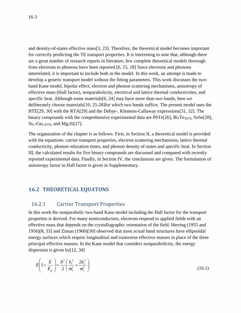
16-2
A generic theoretical model for five bulk thermoelectric materials (PbTe, Bi2Te3, SnSe,
Si0.7Ge0.3, and Mg2Si) has been developed here based on the semiclassical model incorporating
nonparabolicity, two-band Kane model, Hall factor, and the Debye-Callaway model for electrons
and phonons. It is used to calculate thermoelectric transport properties: the Seebeck coefficient,
electrical conductivity, electronic and lattice thermal conductivities at a temperature range from
room temperature up to 1200 K. The present model differs from others: Firstly, thorough
verification of modified electron scattering mechanisms by comparison with reported
experimental data. Secondly, extensive verification of the model with concomitant agreement
between calculations and reported measurements on effective masses, electron and hole
concentrations, Seebeck coefficient, electrical conductivity, and electronic and lattice thermal
conductivities. Thirdly, the present model provides the Fermi energy as a function of temperature
and doping concentration. Fourthly, the velocities of sound are calculated using the Debye model
rather than taken from literature. After verification of the present model, we were able to
examine a recently attracted material of SnSe, indicating a significant improvement on the
dimensionless figure of merit.
16.1 Introduction
Thermoelectric (TE) materials directly convert thermal energy to electricity or vice versa without
moving parts, maintenance, and sounds. Hitherto, they have been used only in niche applications
such as space exploration or electronic temperature control due to their low thermal
efficiencies.[1, 2] It has long been thought that if their efficiencies are improved they could be
used for waste heat recovery or large scale solar power conversion. Since the early 1910s, a great
deal of effort on understanding the physics for TE transport properties recently brought a
remarkable improvement, especially with nanostructures.[3-5] It is known that the modeling of
nanostructures is based on the frame work of bulk structures.[6] Many models and experiments
are reported in the literature.[6-17] Semiclassical theories based on the linearized Boltzmann
transport equation (BTE) with the relaxation time approximation (RTA) have successful
agreement with the experiments even with their limitations (elastic scattering).[6, 18, 19] A
specific model was typically developed for a specific material, which leaves it uncertain whether
it could also work for other materials. The RTA incorporates the electron and phonon scattering
mechanisms, which are of great importance for determining the TE transport properties.[20]
Notably, a variety in the use of electron scattering mechanisms prevails in literature. Ab initio
numerical calculations lead to understanding electron and phonon band structures, dispersion
relations, density-of-states effective masses.[21, 22] However, they are intrinsically incapable of
predicting experimental values due to its inability to handle temperature-dependent band gaps
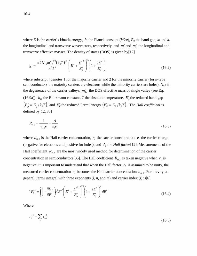
16-3
and density-of-states effective mass[3, 23]. Therefore, the theoretical model becomes important
for correctly predicting the TE transport properties. It is interesting to note that, although there
are a great number of research reports in literature, few complete theoretical models thorough
from electrons to phonons have been reported.[6, 15, 18] Since electrons and phonons
interrelated, it is important to include both in the model. In this work, an attempt is made to
develop a generic transport model without the fitting parameters. This work discusses the two-
band Kane model, bipolar effect, electron and phonon scattering mechanisms, anisotropy of
effective mass (Hall factor), nonparabolicity, electrical and lattice thermal conductivities, and
specific heat. Although some materials[6, 24] may have more than two bands, here we
deliberately choose materials[10, 25-28]for which two bands suffice. The present model uses the
BTE[29, 30] with the RTA[29] and the Debye-, Klemens-Callaway expressions[31, 32]. The
binary compounds with the comprehensive experimental data are PbTe[26], Bi2Te3[25], SnSe[28],
Si0.7Ge0.3[10], and Mg2Si[27].
The organization of the chapter is as follows. First, in Section II, a theoretical model is provided
with the equations: carrier transport properties, electron scattering mechanisms, lattice thermal
conductivity, phonon relaxation times, and phonon density of states and specific heat. In Section
III, the calculated results for five binary compounds are discussed and compared with recently
reported experimental data. Finally, in Section IV, the conclusions are given. The formulation of
anisotropy factor in Hall factor is given in Supplementary.
16.2 THEORETICAL EQUATONS
16.2.1 Carrier Transport Properties
In this work the nonparabolic two-band Kane model including the Hall factor for the transport
properties is derived. For many semiconductors, electrons respond to applied fields with an
effective mass that depends on the crystallographic orientation of the field. Herring (1955 and
1956)[8, 33] and Ziman (1960)[30] observed that most actual band structures have ellipsoidal
energy surfaces which require longitudinal and transverse effective masses in place of the three
principal effective masses. In the Kane model that considers nonparabolicity, the energy
dispersion is given by[12, 34]
t
t
l
l
g m
k
m
k
E
EE
222 2
21
(16.1)
16-4
where E is the carrier’s kinetic energy, the Planck constant (h/2), Eg the band gap, kl and kt
the longitudinal and transverse wavevectors, respectively, and
lm and
tm the longitudinal and
transverse effective masses. The density of states (DOS) is given by[12]
gg
Bidiv
iE
E
E
EE
TkmNg
21
221
2
32
2123
,,
(16.2)
where subscript i denotes 1 for the majority carrier and 2 for the minority carrier (for n-type
semiconductors the majority carriers are electrons while the minority carriers are holes). Nv,i is
the degeneracy of the carrier valleys,
idm , the DOS effective mass of single valley (see Eq.
(16.9a)), Bk the Boltzmann constant, T the absolute temperature,
gE the reduced band gap
TkEE Bgg
, and
FE the reduced Fermi energy TkEE BFF . The Hall coefficient is
defined by[12, 35]
ii
i
iiH
iHen
A
enR
,
,
1
(16.3)
where iHn , is the Hall carrier concentration, in the carrier concentration, ie the carrier charge
(negative for electrons and positive for holes), and iA the Hall factor[12]. Measurements of the
Hall coefficient iHR , are the most widely used method for determination of the carrier
concentration in semiconductors[35]. The Hall coefficient iHR , is taken negative when ie is
negative. It is important to understand that when the Hall factor iA is assumed to be unity, the
measured carrier concentration in becomes the Hall carrier concentration iHn , . For brevity, a
general Fermi integral with three exponents (l, n, and m) and carrier index (i) is[6]
0
232
,0
,
21 dE
E
E
E
EEE
E
fF
m
gg
nl
i
im
il
n (16.4)
Where
j
jii
1
,
1 (16.5)
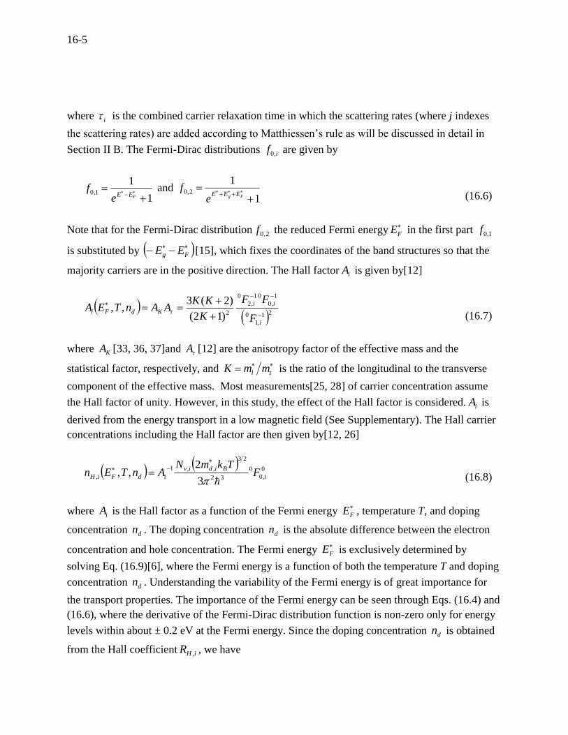
16-5
where i is the combined carrier relaxation time in which the scattering rates (where j indexes
the scattering rates) are added according to Matthiessen’s rule as will be discussed in detail in
Section II B. The Fermi-Dirac distributions if ,0 are given by
1
11,0
FEEe
f and 1
12,0
Fg EEEe
f (16.6)
Note that for the Fermi-Dirac distribution 2,0f the reduced Fermi energy
FE in the first part 1,0f
is substituted by Fg EE [15], which fixes the coordinates of the band structures so that the
majority carriers are in the positive direction. The Hall factor iA is given by[12]
21
,1
0
1
,0
01
,2
0
2)12(
)2(3,,
i
ii
KdFi
F
FF
K
KKAAnTEA
(16.7)
where KA [33, 36, 37]and A [12] are the anisotropy factor of the effective mass and the
statistical factor, respectively, and tl mmK is the ratio of the longitudinal to the transverse
component of the effective mass. Most measurements[25, 28] of carrier concentration assume
the Hall factor of unity. However, in this study, the effect of the Hall factor is considered. iA is
derived from the energy transport in a low magnetic field (See Supplementary). The Hall carrier
concentrations including the Hall factor are then given by[12, 26]
0
,0
0
32
23
,,1
,3
2,, i
Bidiv
idFiH FTkmN
AnTEn
(16.8)
where iA is the Hall factor as a function of the Fermi energy
FE , temperature T, and doping
concentration dn . The doping concentration dn is the absolute difference between the electron
concentration and hole concentration. The Fermi energy
FE is exclusively determined by
solving Eq. (16.9)[6], where the Fermi energy is a function of both the temperature T and doping
concentration dn . Understanding the variability of the Fermi energy is of great importance for
the transport properties. The importance of the Fermi energy can be seen through Eqs. (16.4) and
(16.6), where the derivative of the Fermi-Dirac distribution function is non-zero only for energy
levels within about ± 0.2 eV at the Fermi energy. Since the doping concentration dn is obtained
from the Hall coefficient iHR , , we have
16-6
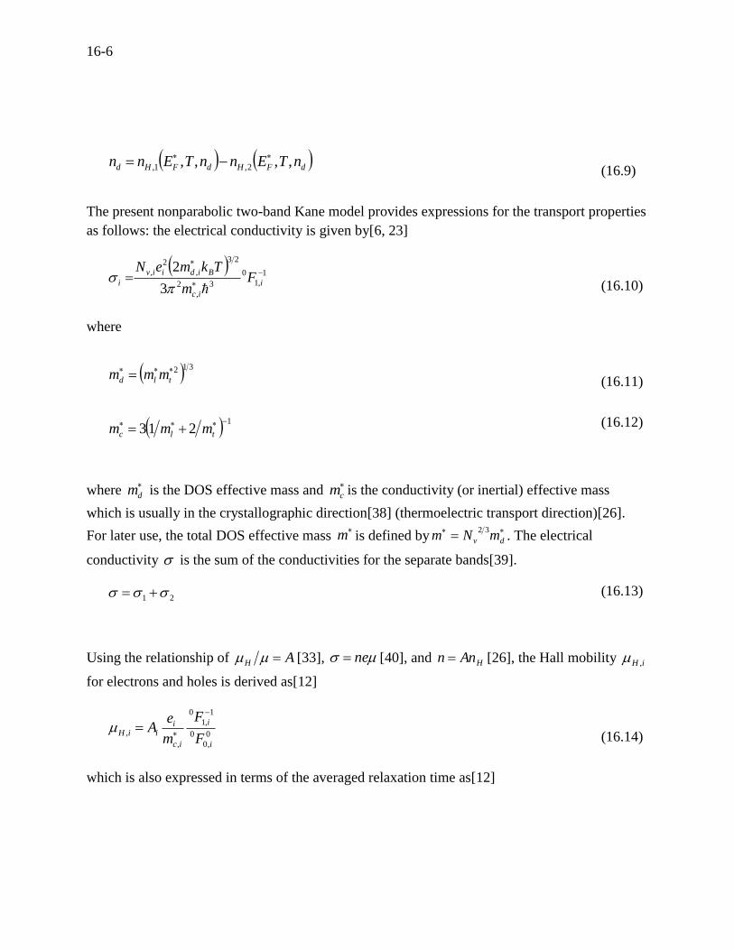
dFHdFHd nTEnnTEnn ,,,, 2,1,
(16.9)
The present nonparabolic two-band Kane model provides expressions for the transport properties
as follows: the electrical conductivity is given by[6, 23]
1
,1
0
3
,
2
23
,
2
,
3
2
i
ic
Bidiiv
i Fm
TkmeN
(16.10)
where
312 tld mmm (16.11)
1213
tlc mmm (16.12)
where
dm is the DOS effective mass and
cm is the conductivity (or inertial) effective mass
which is usually in the crystallographic direction[38] (thermoelectric transport direction)[26].
For later use, the total DOS effective mass m is defined by
dv mNm32
. The electrical
conductivity is the sum of the conductivities for the separate bands[39].
21 (16.13)
Using the relationship of AH [33], ne [40], and HAnn [26], the Hall mobility iH ,
for electrons and holes is derived as[12]
0
,0
0
1
,1
0
,
,
i
i
ic
iiiH
F
F
m
eA
(16.14)
which is also expressed in terms of the averaged relaxation time as[12]
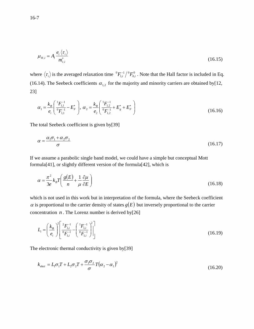
16-7
ic
ii
iiHm
eA
,
,
(16.15)
where i is the averaged relaxation time 0
,0
01
,1
0
ii FF . Note that the Hall factor is included in Eq.
(16.14). The Seebeck coefficients 2,1 for the majority and minority carriers are obtained by[12,
23]
F
i
B EF
F
e
k1
1,1
0
1
1,1
1
1 ,
FgB EE
F
F
e
k1
2,1
0
1
2,1
1
2
2 (16.16)
The total Seebeck coefficient is given by[39]
2211
(16.17)
If we assume a parabolic single band model, we could have a simple but conceptual Mott
formula[41], or slightly different version of the formula[42], which is
En
EgTk
eB
1
3
2
(16.18)
which is not used in this work but in interpretation of the formula, where the Seebeck coefficient
is proportional to the carrier density of states Eg but inversely proportional to the carrier
concentration n . The Lorenz number is derived by[26]
2
1
,1
0
1
,1
1
1
,1
0
1
,1
22
i
i
i
i
i
Bi
F
F
F
F
e
kL
(16.19)
The electronic thermal conductivity is given by[39]
21221
2211
TTLTLkelect
(16.20)
16-8
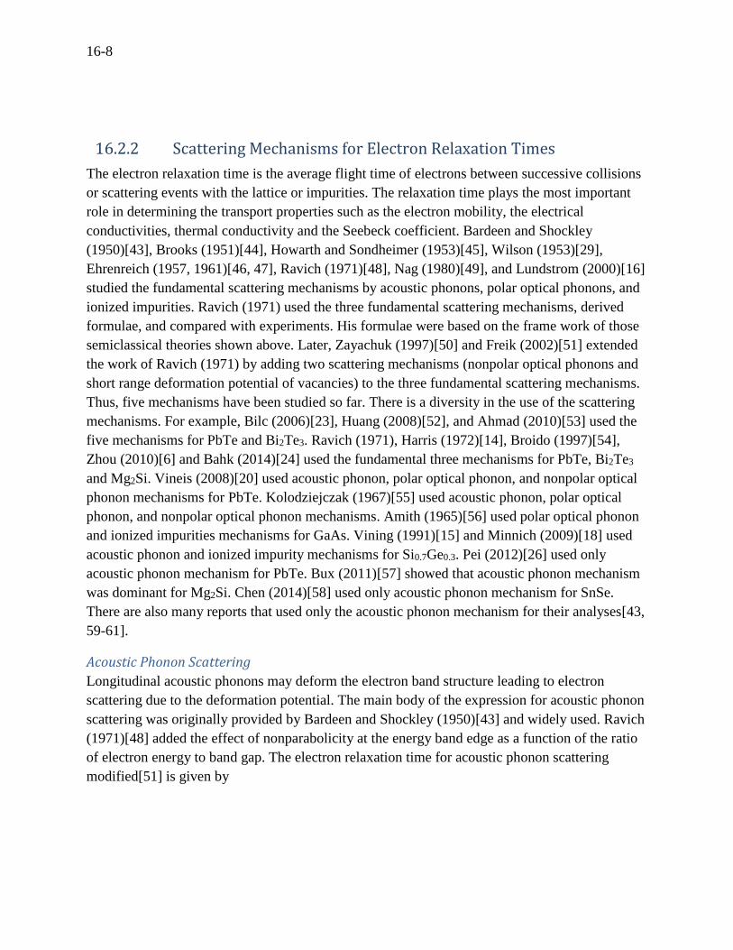
16.2.2 Scattering Mechanisms for Electron Relaxation Times
The electron relaxation time is the average flight time of electrons between successive collisions
or scattering events with the lattice or impurities. The relaxation time plays the most important
role in determining the transport properties such as the electron mobility, the electrical
conductivities, thermal conductivity and the Seebeck coefficient. Bardeen and Shockley
(1950)[43], Brooks (1951)[44], Howarth and Sondheimer (1953)[45], Wilson (1953)[29],
Ehrenreich (1957, 1961)[46, 47], Ravich (1971)[48], Nag (1980)[49], and Lundstrom (2000)[16]
studied the fundamental scattering mechanisms by acoustic phonons, polar optical phonons, and
ionized impurities. Ravich (1971) used the three fundamental scattering mechanisms, derived
formulae, and compared with experiments. His formulae were based on the frame work of those
semiclassical theories shown above. Later, Zayachuk (1997)[50] and Freik (2002)[51] extended
the work of Ravich (1971) by adding two scattering mechanisms (nonpolar optical phonons and
short range deformation potential of vacancies) to the three fundamental scattering mechanisms.
Thus, five mechanisms have been studied so far. There is a diversity in the use of the scattering
mechanisms. For example, Bilc (2006)[23], Huang (2008)[52], and Ahmad (2010)[53] used the
five mechanisms for PbTe and Bi2Te3. Ravich (1971), Harris (1972)[14], Broido (1997)[54],
Zhou (2010)[6] and Bahk (2014)[24] used the fundamental three mechanisms for PbTe, Bi2Te3
and Mg2Si. Vineis (2008)[20] used acoustic phonon, polar optical phonon, and nonpolar optical
phonon mechanisms for PbTe. Kolodziejczak (1967)[55] used acoustic phonon, polar optical
phonon, and nonpolar optical phonon mechanisms. Amith (1965)[56] used polar optical phonon
and ionized impurities mechanisms for GaAs. Vining (1991)[15] and Minnich (2009)[18] used
acoustic phonon and ionized impurity mechanisms for Si0.7Ge0.3. Pei (2012)[26] used only
acoustic phonon mechanism for PbTe. Bux (2011)[57] showed that acoustic phonon mechanism
was dominant for Mg2Si. Chen (2014)[58] used only acoustic phonon mechanism for SnSe.
There are also many reports that used only the acoustic phonon mechanism for their analyses[43,
59-61].
Acoustic Phonon Scattering
Longitudinal acoustic phonons may deform the electron band structure leading to electron
scattering due to the deformation potential. The main body of the expression for acoustic phonon
scattering was originally provided by Bardeen and Shockley (1950)[43] and widely used. Ravich
(1971)[48] added the effect of nonparabolicity at the energy band edge as a function of the ratio
of electron energy to band gap. The electron relaxation time for acoustic phonon scattering
modified[51] is given by
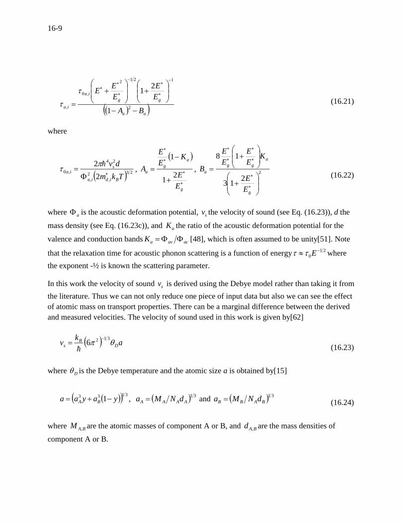
16-9
aa
gg
ia
iaBA
E
E
E
EE
2
1212
,0
,1
21
(16.21)
where
23
,
2
,
24
,0
2
2
Tkm
dv
Bidia
sia
,
g
a
g
a
E
E
KE
E
A2
1
1
, 2
213
18
g
a
gg
a
E
E
KE
E
E
E
B (16.22)
where a is the acoustic deformation potential, sv the velocity of sound (see Eq. (16.23)), d the
mass density (see Eq. (16.23c)), and aK the ratio of the acoustic deformation potential for the
valence and conduction bands acavaK [48], which is often assumed to be unity[51]. Note
that the relaxation time for acoustic phonon scattering is a function of energy21
0
E where
the exponent -½ is known the scattering parameter.
In this work the velocity of sound sv is derived using the Debye model rather than taking it from
the literature. Thus we can not only reduce one piece of input data but also we can see the effect
of atomic mass on transport properties. There can be a marginal difference between the derived
and measured velocities. The velocity of sound used in this work is given by[62]
ak
v DB
s 3126
(16.23)
where D is the Debye temperature and the atomic size a is obtained by[15]
3133 1 yayaa BA , 31
AAAA dNMa and 31
BABB dNMa (16.24)
where BAM , are the atomic masses of component A or B, and BAd , are the mass densities of
component A or B.
16-10
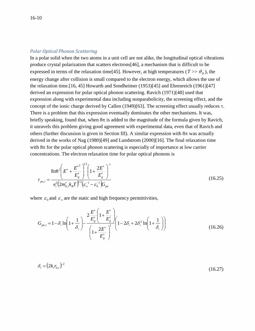
Polar Optical Phonon Scattering
In a polar solid when the two atoms in a unit cell are not alike, the longitudinal optical vibrations
produce crystal polarization that scatters electrons[46], a mechanism that is difficult to be
expressed in terms of the relaxation time[45]. However, at high temperatures (T >> D ), the
energy change after collision is small compared to the electron energy, which allows the use of
the relaxation time.[16, 45] Howarth and Sondheimer (1953)[45] and Ehrenreich (1961)[47]
derived an expression for polar optical phonon scattering. Ravich (1971)[48] used that
expression along with experimental data including nonparabolicity, the screening effect, and the
concept of the ionic charge derived by Callen (1949)[63]. The screening effect usually reduces .
There is a problem that this expression eventually dominates the other mechanisms. It was,
briefly speaking, found that, when 8 is added to the magnitude of the formula given by Ravich,
it unravels this problem giving good agreement with experimental data, even that of Ravich and
others (further discussion is given in Section III). A similar expression with 8 was actually
derived in the works of Nag (1980)[49] and Lundstrom (2000)[16]. The final relaxation time
with 8 for the polar optical phonon scattering is especially of importance at low carrier
concentrations. The electron relaxation time for polar optical phonons is
poBidi
gg
ipo
GTkme
E
E
E
EE
1
0
121
,
2
1212
2
,
2
218
(16.25)
where 0 and are the static and high frequency permittivities,
i
ii
g
gg
i
iipo
E
E
E
E
E
E
G
1
1ln221
21
121
1ln1 2
2, (16.26)
2
,02
iii rk (16.27)
16-11
21
221
,2
g
Bid
iE
EE
Tkmk
(16.28)
21
0
212
,0
3
2123
,
225
,0
21
2
dE
E
E
E
EE
E
fTkmer
gg
iBidi
i
(16.29)
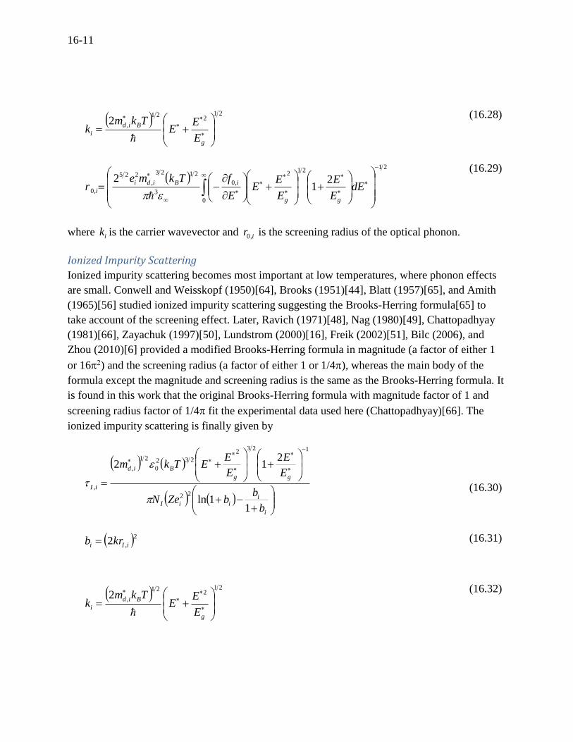
where ik is the carrier wavevector and ir ,0 is the screening radius of the optical phonon.
Ionized Impurity Scattering
Ionized impurity scattering becomes most important at low temperatures, where phonon effects
are small. Conwell and Weisskopf (1950)[64], Brooks (1951)[44], Blatt (1957)[65], and Amith
(1965)[56] studied ionized impurity scattering suggesting the Brooks-Herring formula[65] to
take account of the screening effect. Later, Ravich (1971)[48], Nag (1980)[49], Chattopadhyay
(1981)[66], Zayachuk (1997)[50], Lundstrom (2000)[16], Freik (2002)[51], Bilc (2006), and
Zhou (2010)[6] provided a modified Brooks-Herring formula in magnitude (a factor of either 1
or 16) and the screening radius (a factor of either 1 or 1/4), whereas the main body of the
formula except the magnitude and screening radius is the same as the Brooks-Herring formula. It
is found in this work that the original Brooks-Herring formula with magnitude factor of 1 and
screening radius factor of 1/4 fit the experimental data used here (Chattopadhyay)[66]. The
ionized impurity scattering is finally given by
i
iiiI
gg
Bid
iI
b
bbZeN
E
E
E
EETkm
11ln
212
22
1232
232
0
21
,
,
(16.30)
2,2 iIi krb (16.31)
21
221
,2
g
Bid
iE
EE
Tkmk
(16.32)
16-12
21
0
212
,0
3
2123
,
225
,
21
2
4
1
dE
E
E
E
EE
E
fTkmer
gg
iBidi
iI
(16.33)
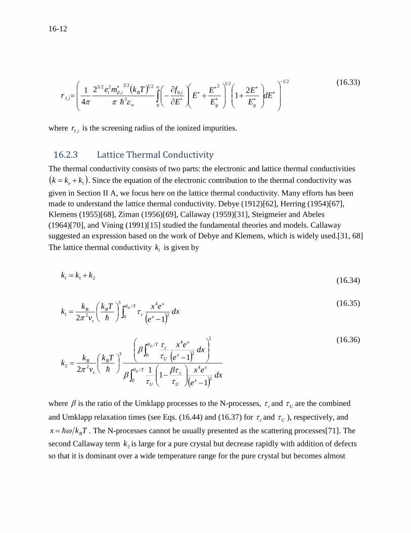
where iIr , is the screening radius of the ionized impurities.
16.2.3 Lattice Thermal Conductivity
The thermal conductivity consists of two parts: the electronic and lattice thermal conductivities
le kkk . Since the equation of the electronic contribution to the thermal conductivity was
given in Section II A, we focus here on the lattice thermal conductivity. Many efforts has been
made to understand the lattice thermal conductivity. Debye (1912)[62], Herring (1954)[67],
Klemens (1955)[68], Ziman (1956)[69], Callaway (1959)[31], Steigmeier and Abeles
(1964)[70], and Vining (1991)[15] studied the fundamental theories and models. Callaway
suggested an expression based on the work of Debye and Klemens, which is widely used.[31, 68]
The lattice thermal conductivity lk is given by
21 kkkl (16.34)
T
x
x
cB
s
B D
dxe
exTk
v
kk
/
0 2
43
21
12
(16.35)
T
x
x
U
c
U
T
x
x
U
c
B
s
B
D
D
dxe
ex
dxe
ex
Tk
v
kk
/
0 2
4
2
/
0 2
4
3
22
11
1
1
2
(16.36)
where is the ratio of the Umklapp processes to the N-processes, c and U are the combined
and Umklapp relaxation times (see Eqs. (16.44) and (16.37) for c and U ), respectively, and
Tkx B . The N-processes cannot be usually presented as the scattering processes[71]. The
second Callaway term 2k is large for a pure crystal but decrease rapidly with addition of defects
so that it is dominant over a wide temperature range for the pure crystal but becomes almost
16-13
negligible for an impure crystal.[71] Most doped crystal compounds that have intrinsic defects
are impure in fact, so that 1kkl .
16.2.4 Phonon Relaxation Times
Extensive studies[72-80] have been made into phonon relaxation times, including normal-mode
processes (N-processes), Umklapp processes, point defects, electron-phonon, and boundary
scattering. We use here the expressions suggested by Steigmeier and Abeles (1964).[70] Vining
(1991)[15] and Minnich (2009)[18] also used those scattering expressions.
Scattering by N-Processes and Umklapp Processes
The Umklapp processes are 3-phonon scattering involving anharmonicity. As mentioned in
Section II C, the N-processes do not directly cause the scattering but help the Umklapp processes
contribute to the scattering. Therefore, they can be expressed in terms of the relaxation time in 1k
even when 2k is neglected in Eq. (16.20a). The Umklapp scattering rate is the inverse of the
relaxation time, which is first studied by Leibfried and Schlömann (1954).[72] Later, a modified
expression including the effect of the N-processes was given by[15, 70, 81]
2
3
2
231
21
1
9
51
4
6
3
20x
T
aMN
DAB
AU
(16.37)
where AN is Avogadro’s number, the Grüneisen anharmonicity parameter, ABM the atomic
mass of compounds A and B, a the mean atomic size (see Eq. (16.24)), and Tkx B .
The N-process scattering rate is given by
11 UN
(16.38)
where 2 is often used for a good approximation.
Scattering by Point Defects
The point defects may include vacancies, isotopes, dislocations, substitute atoms, etc. A defect
with dimensions much smaller than the phonon wavelength can be considered as a point
defect[71]. The scattering is then caused by the difference in mass and the difference in bonding
16-14
between the atoms.[71] The scattering rate for point defects is given by Klemens (1960)[75],
which is
3
4
4
01
4 s
B
PDv
xTk
V
(16.39)
where 0V is the atomic volume (3a ) and the mass-fluctuation-scattering parameter for a binary
compound is given by[70]
22
1a
a
M
Myy s
AB
(16.40)
BA MMM , )1( yMyMM BAAB ,
3aNMd AAB and BA aaa (16.41)
where y is the fraction of component A, d the density of compound and s the strain
parameter.[70]
Scattering by Electron-Phonon
The scattering of phonons by electrons will be active when the band degeneracy temperature is
comparable with the temperature of the lattice.[69] Ziman (1956) derived an expression for the
electron-phonon scattering, which is
216
216
4
3
,
2
1
,
,
2
,
2
1
1ln
4 x
E
xEE
x
E
xEE
rc
sida
iEP
ircFrc
ircFrc
e
ex
dE
vm
(16.42)
where a is the acoustic deformation potential, TkvmE Bsidirc 22
,,
and Tkx B .
Boundary Scattering
The phonon-boundary scattering rate is assumed independent of temperature and frequency. The
boundary scattering rate with an assumption of purely diffuse scattering is given by[30]
16-15
L
vsB 1
(16.43)
where L is the effective length of the sample. The total scattering time can be approximated by
adding the scattering rates in accordance with Matthiessen’s rule,[82]
BEPPDUNc
111111
(16.44)
16.2.5 Phonon Density of States and Specific Heat
This analysis is based on the Debye model, in which the lattice vibrates as if it were an elastic
continuum, but the vibration frequencies cannot exceed a certain maximum value, chosen to
make the total number of modes equal to the total number of classical degrees of freedom. The
Debye model replaces all branches of the vibrational spectrum with three branches, each with the
same linear dispersion relations. The velocity of sound is taken as constant for each branches, as
it would be for a classical elastic continuum. In the Debye model the optical modes are
unceremoniously lumped into the top end of the distribution of acoustic modes, as if they were
merely elastic waves of very short wavelength. Despite its obvious crudity, the Debye
approximation has the great advantage of supreme simplicity. If any one parameter is required to
measure the energy scale of the vibrations of a solid, the Debye temperature is the most
appropriate. If any one function is required to represent the distribution of the lattice frequency,
the phonon density of states is the simplest.[30, 62] The total number of modes N is found by
dividing a sphere in wavevector-space by the volume of the primitive cell 323 6 svVN ,
where V is the volume of the crystal. The phonon density of states for each branch is obtained by
taking derivative of N with respect to leading to 322 2 sph vVg . After all, the phonon
density of states per each branch per mode is obtained by[30, 62]
3
23
D
phg
(16.45)
where is the phonon frequency and D the Debye frequency. Using BDD k (cutoff
frequency), Tkx B , and 233 xTTkg DBph , the Debye specific heat in terms of phg
is then obtained by
16-16
T
phx
x
Bv
D
dxge
exTk
V
Nc
0 2
22
13
(16.46)
or equivalently,
T
x
x
D
Bv
D
dxe
exTk
V
Nc
0 2
43
19
(16.47)
where N is the number of modes, V is the volume of a crystal, and VN is assumed to be the
atomic volume 31 a for a cubic structure[30, 75]. Eq. (16.47) is called the Debye formula[30].
16.2.6 Dimensionless Figure of Merit
The dimensionless figure of merit ZT is defined to represent the performance of the
thermoelectric materials by
Tk
aZT
2
(16.48)
where T is the absolute temperature, a the Seebeck coefficient, the electrical conductivity, and
k the thermal conductivity, which were defined in the preceding section. The commercial value is
1ZT . The higher the dimensionless figure of merit the better the performance.
16.3 RESULTS AND DISCUSSION
16.3.1 Electron or Hole Scattering Mechanisms
Mobility for PbTe
The three fundamental scattering mechanisms (acoustic phonons, polar optical phonons, and
ionized impurities) presented in Section II B are examined here and compared to experiments.
Since iciiiiH meA ,, (Eq. (16.15)), the Hall mobility was best known to represent the
individual or combined scattering mechanisms. Scattering rates that are the reciprocals of the
16-17
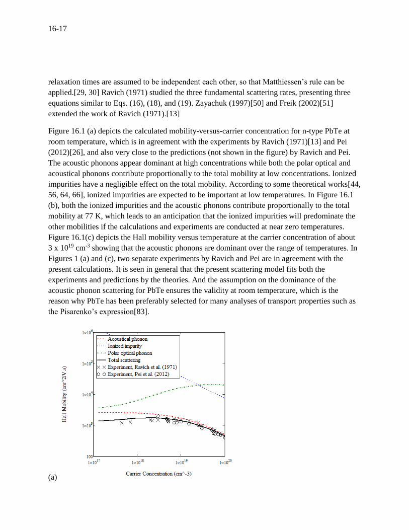
relaxation times are assumed to be independent each other, so that Matthiessen’s rule can be
applied.[29, 30] Ravich (1971) studied the three fundamental scattering rates, presenting three
equations similar to Eqs. (16), (18), and (19). Zayachuk (1997)[50] and Freik (2002)[51]
extended the work of Ravich (1971).[13]
Figure 16.1 (a) depicts the calculated mobility-versus-carrier concentration for n-type PbTe at
room temperature, which is in agreement with the experiments by Ravich (1971)[13] and Pei
(2012)[26], and also very close to the predictions (not shown in the figure) by Ravich and Pei.
The acoustic phonons appear dominant at high concentrations while both the polar optical and
acoustical phonons contribute proportionally to the total mobility at low concentrations. Ionized
impurities have a negligible effect on the total mobility. According to some theoretical works[44,
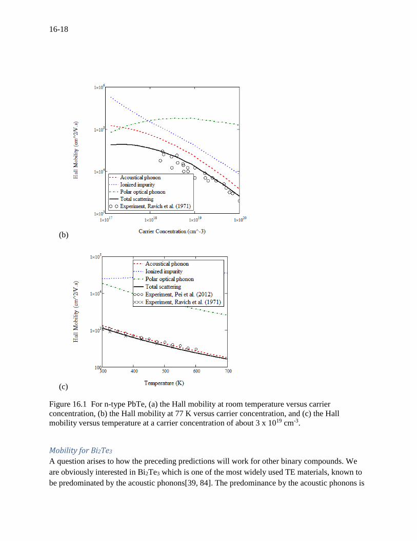
56, 64, 66], ionized impurities are expected to be important at low temperatures. In Figure 16.1
(b), both the ionized impurities and the acoustic phonons contribute proportionally to the total
mobility at 77 K, which leads to an anticipation that the ionized impurities will predominate the
other mobilities if the calculations and experiments are conducted at near zero temperatures.
Figure 16.1(c) depicts the Hall mobility versus temperature at the carrier concentration of about
3 x 1019 cm-3 showing that the acoustic phonons are dominant over the range of temperatures. In
Figures 1 (a) and (c), two separate experiments by Ravich and Pei are in agreement with the
present calculations. It is seen in general that the present scattering model fits both the
experiments and predictions by the theories. And the assumption on the dominance of the
acoustic phonon scattering for PbTe ensures the validity at room temperature, which is the
reason why PbTe has been preferably selected for many analyses of transport properties such as
the Pisarenko’s expression[83].
(a)
16-18
(b)
(c)
Figure 16.1 For n-type PbTe, (a) the Hall mobility at room temperature versus carrier
concentration, (b) the Hall mobility at 77 K versus carrier concentration, and (c) the Hall
mobility versus temperature at a carrier concentration of about 3 x 1019 cm-3.
Mobility for Bi2Te3
A question arises to how the preceding predictions will work for other binary compounds. We
are obviously interested in Bi2Te3 which is one of the most widely used TE materials, known to
be predominated by the acoustic phonons[39, 84]. The predominance by the acoustic phonons is
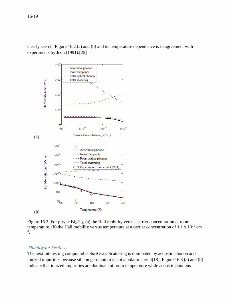
16-19
clearly seen in Figure 16.2 (a) and (b) and its temperature dependence is in agreement with
experiments by Jeon (1991).[25]
(a)
(b)
Figure 16.2 For p-type Bi2Te3, (a) the Hall mobility versus carrier concentration at room
temperature, (b) the Hall mobility versus temperature at a carrier concentration of 1.1 x 1019 cm-
3.
Mobility for Si0.7Ge0.3
The next interesting compound is Si0.7Ge0.3. Scattering is dominated by acoustic phonon and
ionized impurities because silicon germanium is not a polar material[18]. Figure 16.3 (a) and (b)
indicate that ionized impurities are dominant at room temperature while acoustic phonons
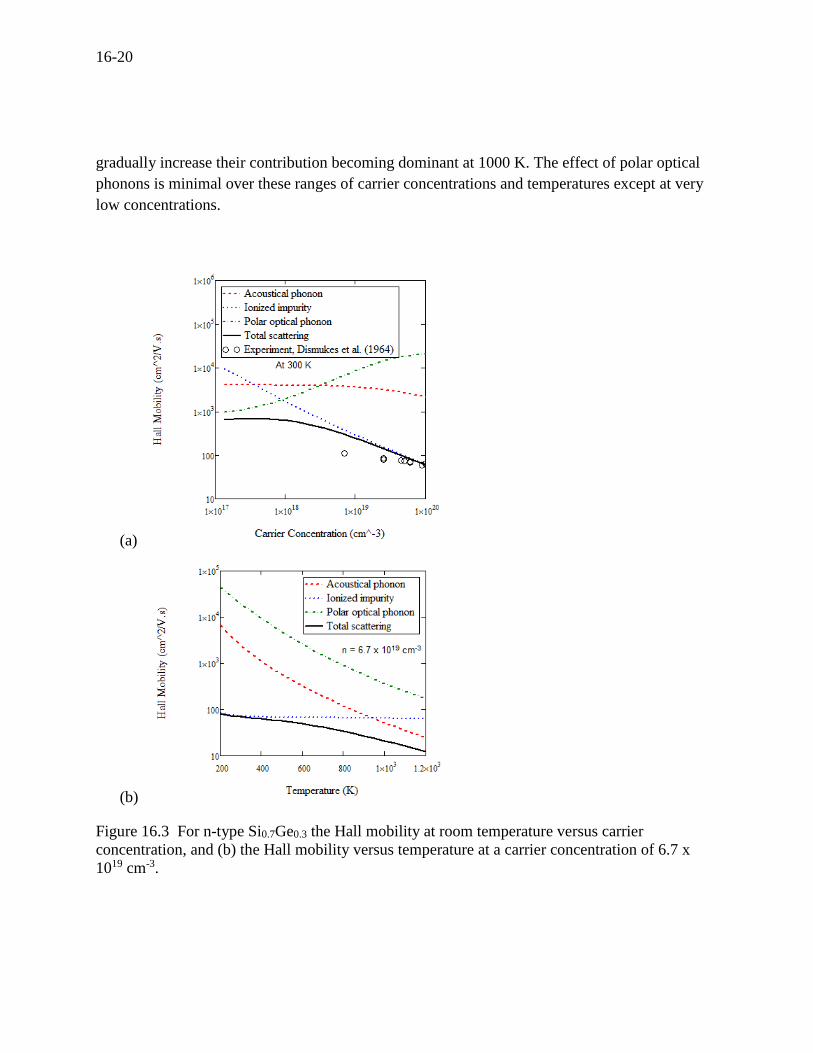
16-20
gradually increase their contribution becoming dominant at 1000 K. The effect of polar optical
phonons is minimal over these ranges of carrier concentrations and temperatures except at very
low concentrations.
(a)
(b)
Figure 16.3 For n-type Si0.7Ge0.3 the Hall mobility at room temperature versus carrier
concentration, and (b) the Hall mobility versus temperature at a carrier concentration of 6.7 x
1019 cm-3.
16-21
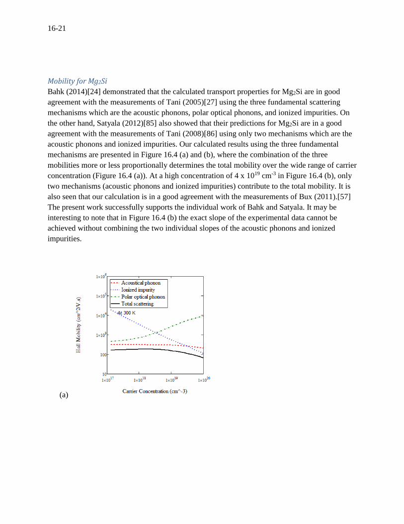
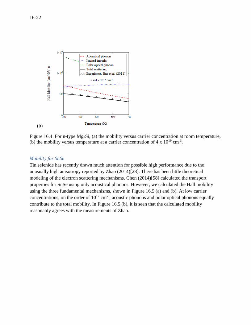
Mobility for Mg2Si
Bahk (2014)[24] demonstrated that the calculated transport properties for Mg2Si are in good
agreement with the measurements of Tani (2005)[27] using the three fundamental scattering
mechanisms which are the acoustic phonons, polar optical phonons, and ionized impurities. On
the other hand, Satyala (2012)[85] also showed that their predictions for Mg2Si are in a good
agreement with the measurements of Tani (2008)[86] using only two mechanisms which are the
acoustic phonons and ionized impurities. Our calculated results using the three fundamental
mechanisms are presented in Figure 16.4 (a) and (b), where the combination of the three
mobilities more or less proportionally determines the total mobility over the wide range of carrier
concentration (Figure 16.4 (a)). At a high concentration of 4 x 1019 cm-3 in Figure 16.4 (b), only
two mechanisms (acoustic phonons and ionized impurities) contribute to the total mobility. It is
also seen that our calculation is in a good agreement with the measurements of Bux (2011).[57]
The present work successfully supports the individual work of Bahk and Satyala. It may be
interesting to note that in Figure 16.4 (b) the exact slope of the experimental data cannot be
achieved without combining the two individual slopes of the acoustic phonons and ionized
impurities.
(a)
16-22
(b)
Figure 16.4 For n-type Mg2Si, (a) the mobility versus carrier concentration at room temperature,
(b) the mobility versus temperature at a carrier concentration of 4 x 1019 cm-3.
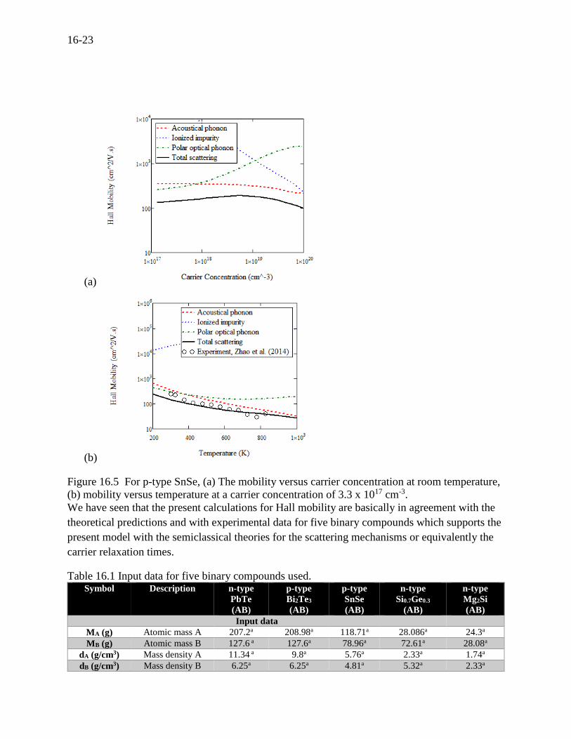
Mobility for SnSe
Tin selenide has recently drawn much attention for possible high performance due to the
unusually high anisotropy reported by Zhao (2014)[28]. There has been little theoretical
modeling of the electron scattering mechanisms. Chen (2014)[58] calculated the transport
properties for SnSe using only acoustical phonons. However, we calculated the Hall mobility
using the three fundamental mechanisms, shown in Figure 16.5 (a) and (b). At low carrier
concentrations, on the order of 1017 cm-3, acoustic phonons and polar optical phonons equally
contribute to the total mobility. In Figure 16.5 (b), it is seen that the calculated mobility
reasonably agrees with the measurements of Zhao.
16-23
(a)
(b)
Figure 16.5 For p-type SnSe, (a) The mobility versus carrier concentration at room temperature,
(b) mobility versus temperature at a carrier concentration of 3.3 x 1017 cm-3.
We have seen that the present calculations for Hall mobility are basically in agreement with the
theoretical predictions and with experimental data for five binary compounds which supports the
present model with the semiclassical theories for the scattering mechanisms or equivalently the
carrier relaxation times.
Table 16.1 Input data for five binary compounds used. Symbol Description n-type
PbTe
(AB)
p-type
Bi2Te3
(AB)
p-type
SnSe
(AB)
n-type
Si0.7Ge0.3
(AB)
n-type
Mg2Si
(AB)
Input data
MA (g) Atomic mass A 207.2a 208.98a 118.71a 28.086a 24.3a
MB (g) Atomic mass B 127.6 a 127.6a 78.96a 72.61a 28.08a
dA (g/cm3) Mass density A 11.34 a 9.8a 5.76a 2.33a 1.74a
dB (g/cm3) Mass density B 6.25a 6.25a 4.81a 5.32a 2.33a
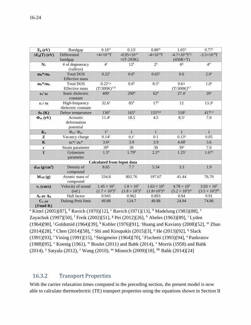
16-24
Eg (eV) Bandgap 0.18 b 0.13j 0.86m 1.05q 0.77v
∆Eg(T) (eV) Differential
bandgap
+4×10⁻⁴T -0.95×10⁻⁴
×(T-293K)
-4×10⁻⁴T -4.7×10⁻⁴T2/
(450K+T)
-3.5×10⁻⁴T
Nv # of degeneracy
(valleys)
4c 12k 2n 6q 4w
mh*/mo Total DOS
Effective mass
0.22c 0.6k 0.65o 0.6 2.0x
me*/mo Total DOS
Effective mass
0.22c×
(T/300K)1/2i
0.6k 8.5o 0.6×
(T/300K)0.7
1.0x
εs/ ε0 Static dielectric
constant
400c 290d 62d 27.4r 20y
ε∞/ ε0 High-frequency
dielectric constant
32.6c 85d 17d 12 13.3y
θD (K) Debye temperature 136d 165d 155m,p 518s 417z,y
Фac (eV) Acoustic
deformation
potential
11.4e 18.5 4.5 8.5s 7.0
Ka Фav/ Фac 1f 1 1 1 1
Z Vacancy charge 0.14e 0.1l 0.1 0.13u 0.05
K ml*/ mt* 3.6g 3.9 3.9 4.68t 3.6
є Strain parameter 39h 39 39 39s 7.0
ϒ Grüneisen
parameter
1.5d 1.79d 2.2m 1.25s 1.67z
Calculated from Input data
dAB (g/cm3) Density of
compound
8.65 7.7 5.34 3.3 1.9
MAB (g) Atomic mass of
compound
334.8 802.76 197.67 41.44 76.70
vs (cm/s) Velocity of sound
(ref.)
1.45 × 10⁵
(1.7 × 10⁵)d
1.8 × 10⁵
(1.8 × 10⁵)d
1.63 × 10⁵
(1.8×10⁵)m
4.78 × 10⁵
(5.2 × 10⁵)aa
3.93 × 10⁵
(3.5 × 10⁵)bb
Ae or Ah Hall factor 0.945 0.962 0.893 0.94 0.91
Cv_DP
(J/mol·K)
Dulong-Petit limit 49.88 124.7 49.88 24.94 74.86
a Kittel (2005)[87], b Ravich (1970)[12], c Ravich (1971)[13], d Madelung (1983)[88], e
Zayachuk (1997)[50], f Freik (2002)[51], g Pei (2012)[26], h Abeles (1963)[89], i Lyden
(1964)[90], j Goldsmid (1964)[39], k Kohler (1976)[91], l Huang and Kaviany (2008)[52], m Zhao
(2014)[28], n Chen (2014)[58], o Shi and Kioupakis (2015)[3], p He (2013)[92], q Slack
(1991)[93], r Vining (1991)[15], s Steigmeier (1964)[70], t Fischetti (1993)[94], u Pankratov
(1988)[95], v Koenig (1961), w Boulet (2011) and Bahk (2014), x Morris (1958) and Bahk
(2014), y Satyala (2012), z Wang (2010), aa Minnich (2009)[18], bb Bahk (2014)[24]
16.3.2 Transport Properties
With the carrier relaxation times computed in the preceding section, the present model is now
able to calculate thermoelectric (TE) transport properties using the equations shown in Section II
16-25
A and the input data listed in Table 16.1. There are always small disagreements between models
and measurements. The disagreements may be here managed by varying the deformation
potential for electrons and the Grüneisen parameter for phonons.
Transport Properties for n-type PbTe
The single crystals of lead telluride have been well known since the early 1950s for
thermoelectric generators at a mid-temperature range from 500 K – 800K.[13, 59, 96-100] The
effective mass for n-type PbTe was measured by Ravich (1971)[13] as 0.22 mo (where mo is the
free electron mass) and also predicted with the ab initio numerical calculations by Vineis
(2008)[20] to be 0.23 mo. The temperature-dependent total DOS effective mass and the
degeneracy of band valleys used are 0.22×(T/300K)1/2 and 4 from Table 16.1, respectively,
which are in good agreement with measurement and ab initio calculations.[48, 90] The first
calculation is to determine the Fermi energy using Eq. (16.8), which is a function of doping
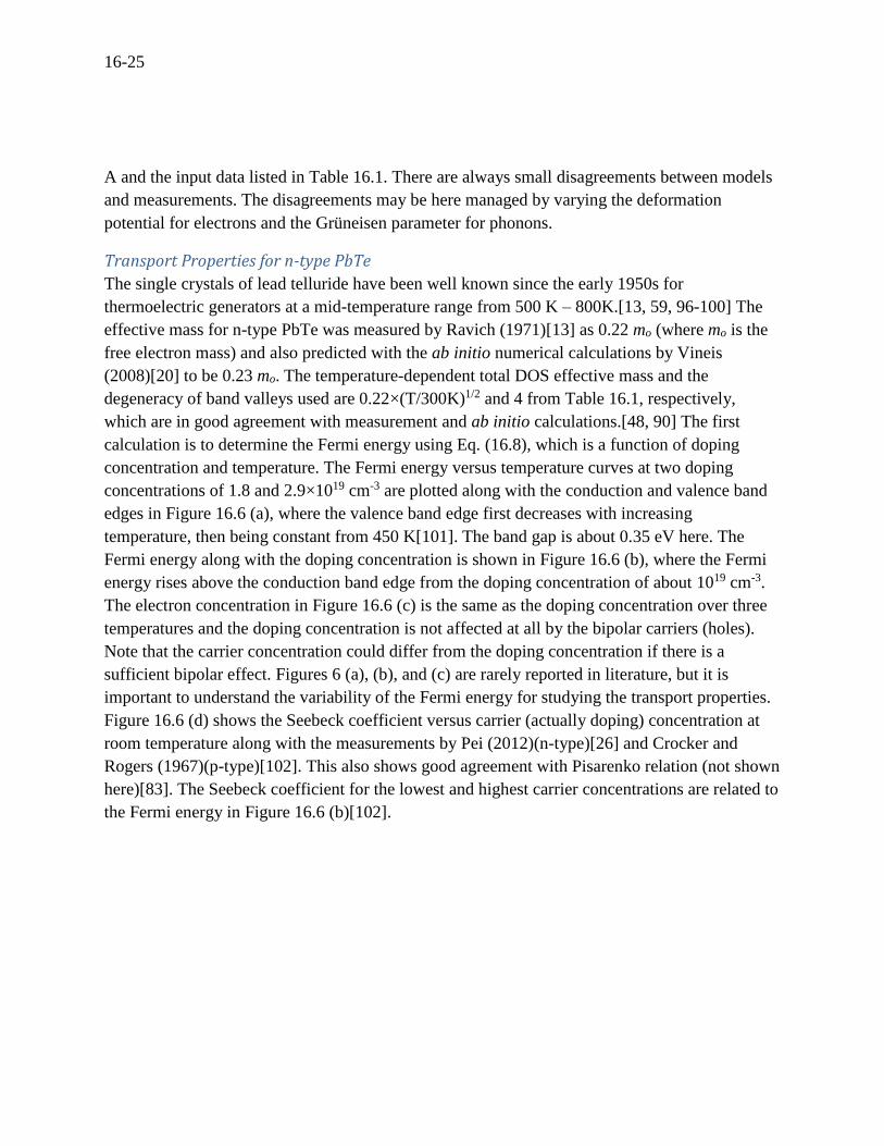
concentration and temperature. The Fermi energy versus temperature curves at two doping
concentrations of 1.8 and 2.9×1019 cm-3 are plotted along with the conduction and valence band
edges in Figure 16.6 (a), where the valence band edge first decreases with increasing
temperature, then being constant from 450 K[101]. The band gap is about 0.35 eV here. The
Fermi energy along with the doping concentration is shown in Figure 16.6 (b), where the Fermi
energy rises above the conduction band edge from the doping concentration of about 1019 cm-3.
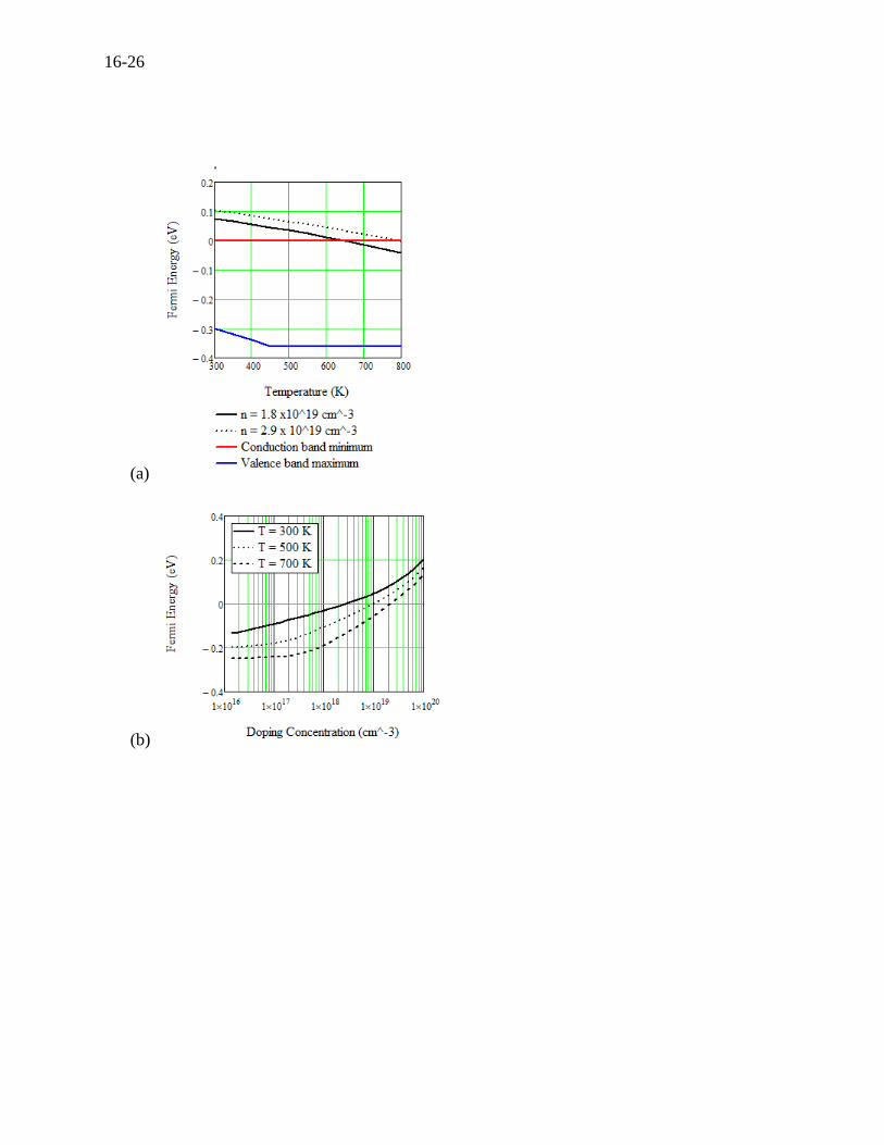
The electron concentration in Figure 16.6 (c) is the same as the doping concentration over three
temperatures and the doping concentration is not affected at all by the bipolar carriers (holes).
Note that the carrier concentration could differ from the doping concentration if there is a
sufficient bipolar effect. Figures 6 (a), (b), and (c) are rarely reported in literature, but it is
important to understand the variability of the Fermi energy for studying the transport properties.
Figure 16.6 (d) shows the Seebeck coefficient versus carrier (actually doping) concentration at
room temperature along with the measurements by Pei (2012)(n-type)[26] and Crocker and
Rogers (1967)(p-type)[102]. This also shows good agreement with Pisarenko relation (not shown
here)[83]. The Seebeck coefficient for the lowest and highest carrier concentrations are related to
the Fermi energy in Figure 16.6 (b)[102].
16-26
(a)
(b)
16-27
(c)
(d)
Figure 16.6 For n-type PbTe, (a) Fermi energy versus temperature, (b) Fermi energy versus
doping concentration, (c) Carrier concentration versus temperature, and (d) Seebeck coefficient
versus doping concentration at room temperature along with measurements by Pei (2012)(n-
type)[26] and Crocker and Rogers (1967)(p-type)[102].
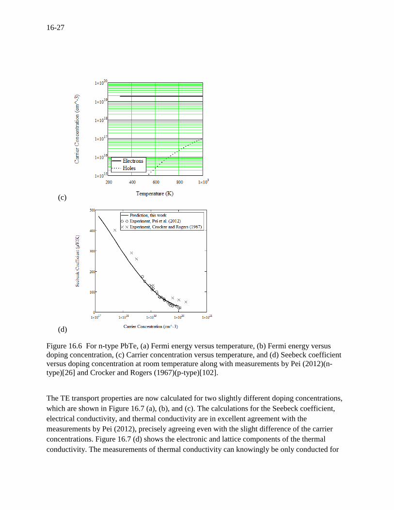
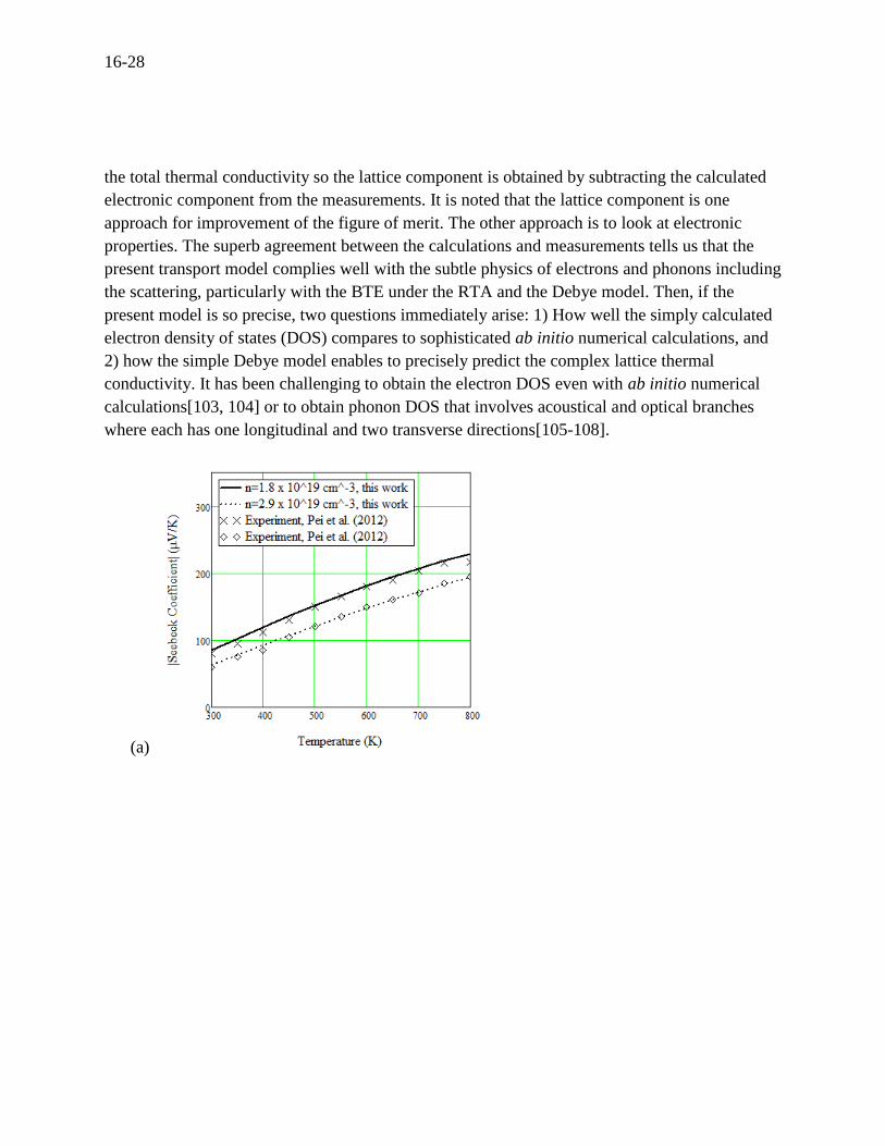
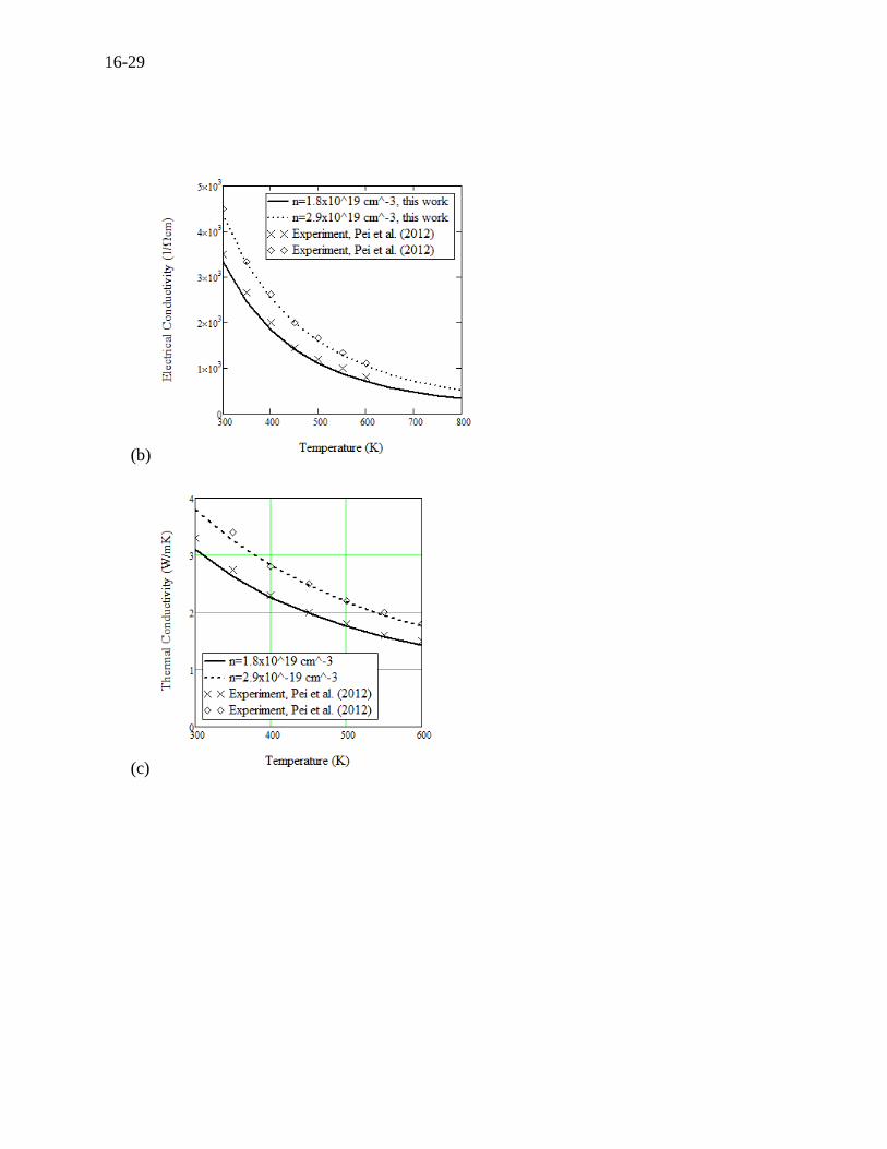
The TE transport properties are now calculated for two slightly different doping concentrations,
which are shown in Figure 16.7 (a), (b), and (c). The calculations for the Seebeck coefficient,
electrical conductivity, and thermal conductivity are in excellent agreement with the
measurements by Pei (2012), precisely agreeing even with the slight difference of the carrier
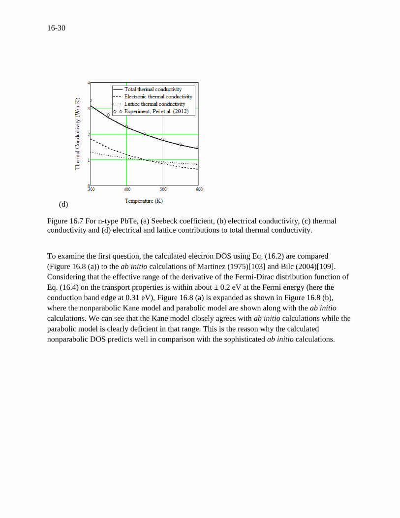
concentrations. Figure 16.7 (d) shows the electronic and lattice components of the thermal
conductivity. The measurements of thermal conductivity can knowingly be only conducted for
16-28
the total thermal conductivity so the lattice component is obtained by subtracting the calculated
electronic component from the measurements. It is noted that the lattice component is one
approach for improvement of the figure of merit. The other approach is to look at electronic
properties. The superb agreement between the calculations and measurements tells us that the
present transport model complies well with the subtle physics of electrons and phonons including
the scattering, particularly with the BTE under the RTA and the Debye model. Then, if the
present model is so precise, two questions immediately arise: 1) How well the simply calculated
electron density of states (DOS) compares to sophisticated ab initio numerical calculations, and
2) how the simple Debye model enables to precisely predict the complex lattice thermal
conductivity. It has been challenging to obtain the electron DOS even with ab initio numerical
calculations[103, 104] or to obtain phonon DOS that involves acoustical and optical branches
where each has one longitudinal and two transverse directions[105-108].
(a)
16-29
(b)
(c)
16-30
(d)
Figure 16.7 For n-type PbTe, (a) Seebeck coefficient, (b) electrical conductivity, (c) thermal
conductivity and (d) electrical and lattice contributions to total thermal conductivity.
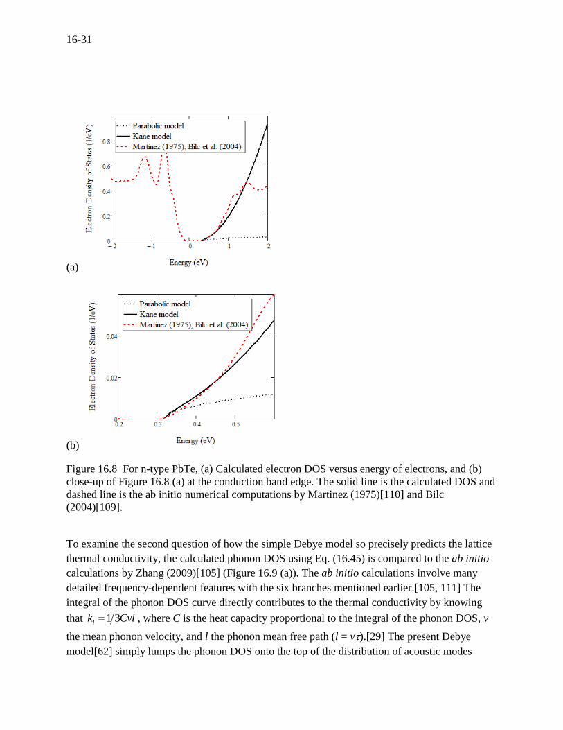
To examine the first question, the calculated electron DOS using Eq. (16.2) are compared
(Figure 16.8 (a)) to the ab initio calculations of Martinez (1975)[103] and Bilc (2004)[109].
Considering that the effective range of the derivative of the Fermi-Dirac distribution function of
Eq. (16.4) on the transport properties is within about ± 0.2 eV at the Fermi energy (here the
conduction band edge at 0.31 eV), Figure 16.8 (a) is expanded as shown in Figure 16.8 (b),
where the nonparabolic Kane model and parabolic model are shown along with the ab initio
calculations. We can see that the Kane model closely agrees with ab initio calculations while the
parabolic model is clearly deficient in that range. This is the reason why the calculated
nonparabolic DOS predicts well in comparison with the sophisticated ab initio calculations.
16-31
(a)
(b)
Figure 16.8 For n-type PbTe, (a) Calculated electron DOS versus energy of electrons, and (b)
close-up of Figure 16.8 (a) at the conduction band edge. The solid line is the calculated DOS and
dashed line is the ab initio numerical computations by Martinez (1975)[110] and Bilc
(2004)[109].
To examine the second question of how the simple Debye model so precisely predicts the lattice
thermal conductivity, the calculated phonon DOS using Eq. (16.45) is compared to the ab initio
calculations by Zhang (2009)[105] (Figure 16.9 (a)). The ab initio calculations involve many
detailed frequency-dependent features with the six branches mentioned earlier.[105, 111] The
integral of the phonon DOS curve directly contributes to the thermal conductivity by knowing
that Cvlkl 31 , where C is the heat capacity proportional to the integral of the phonon DOS, v
the mean phonon velocity, and l the phonon mean free path (l = v).[29] The present Debye
model[62] simply lumps the phonon DOS onto the top of the distribution of acoustic modes
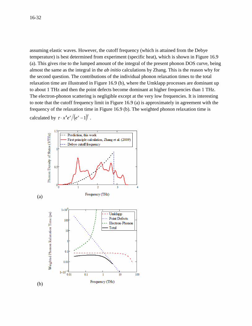
16-32
assuming elastic waves. However, the cutoff frequency (which is attained from the Debye
temperature) is best determined from experiment (specific heat), which is shown in Figure 16.9
(a). This gives rise to the lumped amount of the integral of the present phonon DOS curve, being
almost the same as the integral in the ab initio calculations by Zhang. This is the reason why for
the second question. The contributions of the individual phonon relaxation times to the total
relaxation time are illustrated in Figure 16.9 (b), where the Umklapp processes are dominant up
to about 1 THz and then the point defects become dominant at higher frequencies than 1 THz.
The electron-phonon scattering is negligible except at the very low frequencies. It is interesting
to note that the cutoff frequency limit in Figure 16.9 (a) is approximately in agreement with the
frequency of the relaxation time in Figure 16.9 (b). The weighted phonon relaxation time is
calculated by 24 1 xx eex .
(a)
(b)
16-33
Figure 16.9 For n-type PbTe, (a) calculated phonon DOS versus frequency [105], and (b)
weighted phonon relaxation time versus frequency.
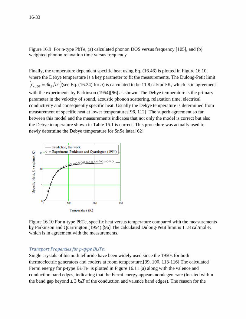
Finally, the temperature dependent specific heat using Eq. (16.46) is plotted in Figure 16.10,
where the Debye temperature is a key parameter to fit the measurements. The Dulong-Petit limit
3
_ 3 akc BDPv (see Eq. (16.24) for a) is calculated to be 11.8 cal/mol·K, which is in agreement
with the experiments by Parkinson (1954)[96] as shown. The Debye temperature is the primary
parameter in the velocity of sound, acoustic phonon scattering, relaxation time, electrical
conductivity and consequently specific heat. Usually the Debye temperature is determined from
measurement of specific heat at lower temperatures[96, 112]. The superb agreement so far
between this model and the measurements indicates that not only the model is correct but also
the Debye temperature shown in Table 16.1 is correct. This procedure was actually used to
newly determine the Debye temperature for SnSe later.[62]
Figure 16.10 For n-type PbTe, specific heat versus temperature compared with the measurements
by Parkinson and Quarrington (1954).[96] The calculated Dulong-Petit limit is 11.8 cal/mol·K
which is in agreement with the measurements.
Transport Properties for p-type Bi2Te3
Single crystals of bismuth telluride have been widely used since the 1950s for both
thermoelectric generators and coolers at room temperature.[39, 100, 113-116] The calculated
Fermi energy for p-type Bi2Te3 is plotted in Figure 16.11 (a) along with the valence and
conduction band edges, indicating that the Fermi energy appears nondegenerate (located within
the band gap beyond ± 3 kBT of the conduction and valence band edges). The reason for the
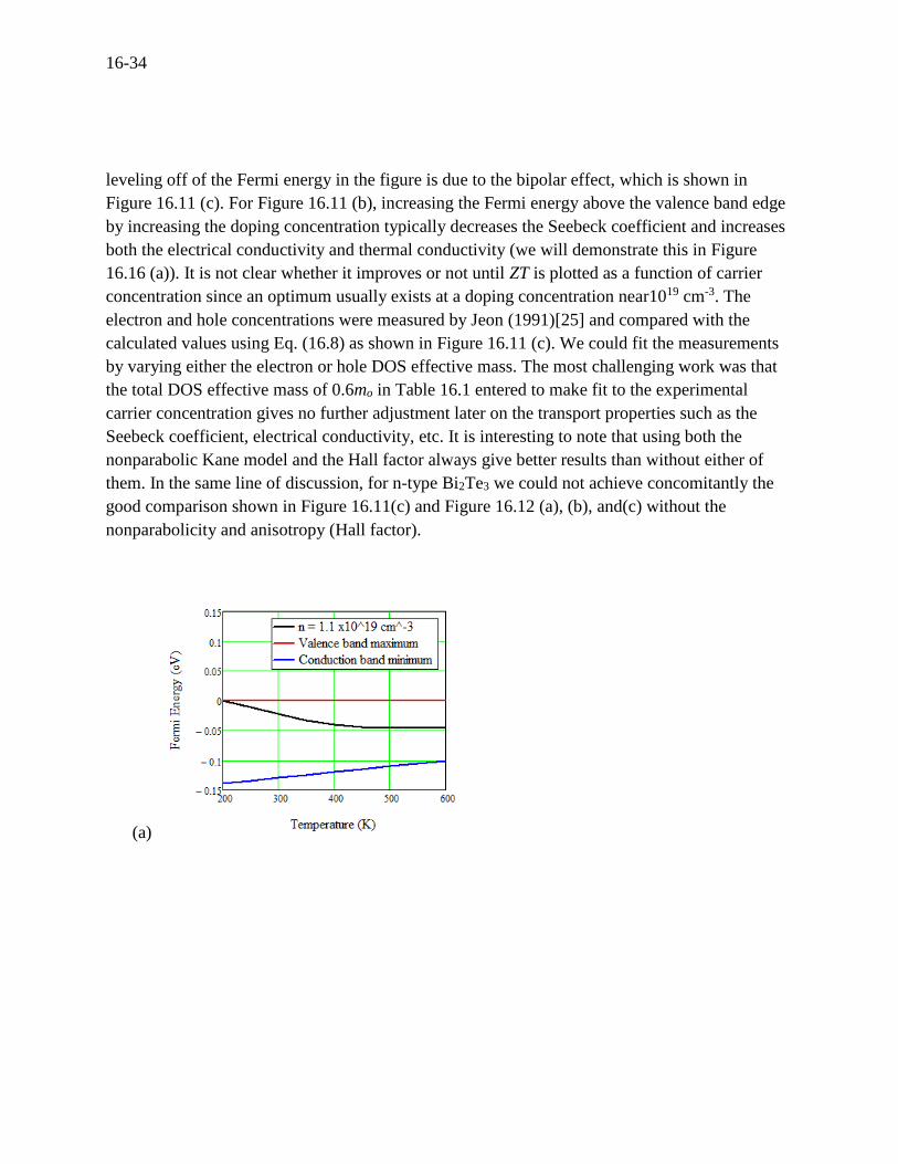
16-34
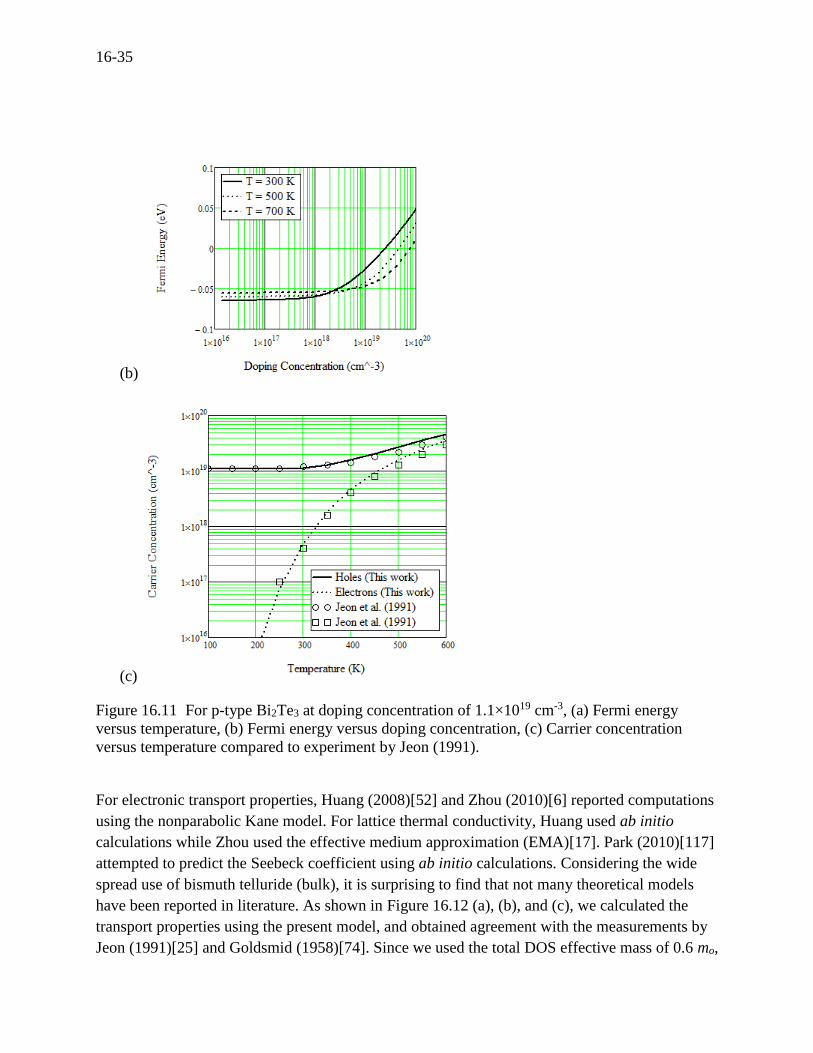
leveling off of the Fermi energy in the figure is due to the bipolar effect, which is shown in
Figure 16.11 (c). For Figure 16.11 (b), increasing the Fermi energy above the valence band edge
by increasing the doping concentration typically decreases the Seebeck coefficient and increases
both the electrical conductivity and thermal conductivity (we will demonstrate this in Figure
16.16 (a)). It is not clear whether it improves or not until ZT is plotted as a function of carrier
concentration since an optimum usually exists at a doping concentration near1019 cm-3. The
electron and hole concentrations were measured by Jeon (1991)[25] and compared with the
calculated values using Eq. (16.8) as shown in Figure 16.11 (c). We could fit the measurements
by varying either the electron or hole DOS effective mass. The most challenging work was that
the total DOS effective mass of 0.6mo in Table 16.1 entered to make fit to the experimental
carrier concentration gives no further adjustment later on the transport properties such as the
Seebeck coefficient, electrical conductivity, etc. It is interesting to note that using both the
nonparabolic Kane model and the Hall factor always give better results than without either of
them. In the same line of discussion, for n-type Bi2Te3 we could not achieve concomitantly the
good comparison shown in Figure 16.11(c) and Figure 16.12 (a), (b), and(c) without the
nonparabolicity and anisotropy (Hall factor).
(a)
16-35
(b)
(c)
Figure 16.11 For p-type Bi2Te3 at doping concentration of 1.1×1019 cm-3, (a) Fermi energy
versus temperature, (b) Fermi energy versus doping concentration, (c) Carrier concentration
versus temperature compared to experiment by Jeon (1991).
For electronic transport properties, Huang (2008)[52] and Zhou (2010)[6] reported computations
using the nonparabolic Kane model. For lattice thermal conductivity, Huang used ab initio
calculations while Zhou used the effective medium approximation (EMA)[17]. Park (2010)[117]
attempted to predict the Seebeck coefficient using ab initio calculations. Considering the wide
spread use of bismuth telluride (bulk), it is surprising to find that not many theoretical models
have been reported in literature. As shown in Figure 16.12 (a), (b), and (c), we calculated the
transport properties using the present model, and obtained agreement with the measurements by
Jeon (1991)[25] and Goldsmid (1958)[74]. Since we used the total DOS effective mass of 0.6 mo,
16-36
the DOS effective mass of a single valley using the degeneracy (multivalley) of 12 valleys is
0.11 mo by using dv mNm32
, whereby 0.11 mo used in this work is close to 0.106 mo measured
by Kohler (1976)[116] and also 0.11 mo calculated by ab initio method by Kim (2005)[22]. Most
works[39, 91, 118-120] used the degeneracy of 6 valleys except a few ab initio calculations used
the degeneracy of 12 valleys[21, 22, 52]. Decreasing lattice thermal conductivity is important for
seeking a high figure of merit.[121] Here we present the lattice thermal conductivity in Figure
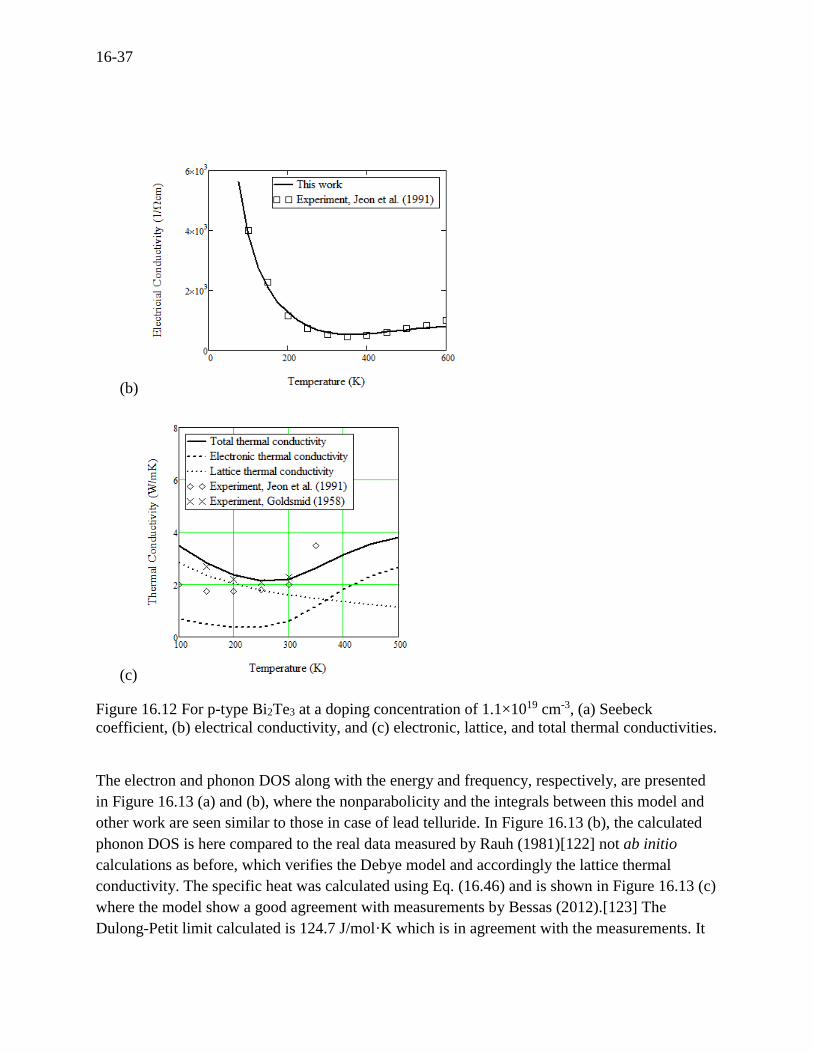
16.12 (c), where the lattice thermal conductivity is dominant up to 300 K while the electronic
thermal conductivity proportionally becomes significant and dominant at higher temperatures,
obviously, due to the bipolar effect in Figure 16.11 (c). For this material, the bipolar effect
negatively acts on the ZT, which leads to room for improvement if the bipolar effect is delayed or
eliminated by a doping technique. The lattice thermal conductivity is mainly determined by the
Umklapp processes where the Grüneisen parameter is the important factor as shown in Eq.
(16.37). Therefore, we make a fine adjustment of the lattice thermal conductivity curve only in
magnitude by adjusting the Grüneisen parameter to be 1.79. This is also in agreement with the
experimental value given by Madelung (1983)[88].
(a)
16-37
(b)
(c)
Figure 16.12 For p-type Bi2Te3 at a doping concentration of 1.1×1019 cm-3, (a) Seebeck
coefficient, (b) electrical conductivity, and (c) electronic, lattice, and total thermal conductivities.
The electron and phonon DOS along with the energy and frequency, respectively, are presented
in Figure 16.13 (a) and (b), where the nonparabolicity and the integrals between this model and
other work are seen similar to those in case of lead telluride. In Figure 16.13 (b), the calculated
phonon DOS is here compared to the real data measured by Rauh (1981)[122] not ab initio
calculations as before, which verifies the Debye model and accordingly the lattice thermal
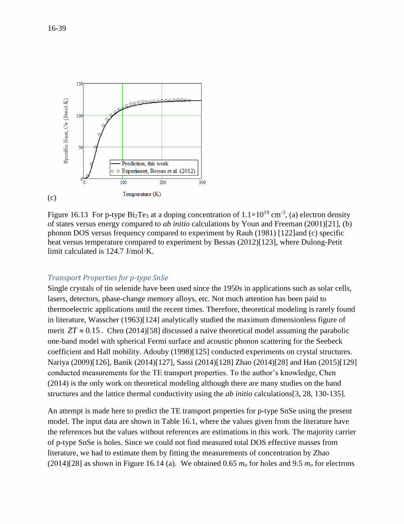
conductivity. The specific heat was calculated using Eq. (16.46) and is shown in Figure 16.13 (c)
where the model show a good agreement with measurements by Bessas (2012).[123] The
Dulong-Petit limit calculated is 124.7 J/mol·K which is in agreement with the measurements. It
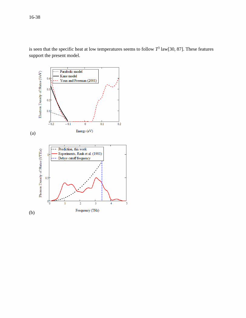
16-38
is seen that the specific heat at low temperatures seems to follow T3 law[30, 87]. These features
support the present model.
(a)
(b)
16-39
(c)
Figure 16.13 For p-type Bi2Te3 at a doping concentration of 1.1×1019 cm-3, (a) electron density
of states versus energy compared to ab initio calculations by Youn and Freeman (2001)[21], (b)
phonon DOS versus frequency compared to experiment by Rauh (1981) [122]and (c) specific
heat versus temperature compared to experiment by Bessas (2012)[123], where Dulong-Petit
limit calculated is 124.7 J/mol·K.
Transport Properties for p-type SnSe
Single crystals of tin selenide have been used since the 1950s in applications such as solar cells,
lasers, detectors, phase-change memory alloys, etc. Not much attention has been paid to
thermoelectric applications until the recent times. Therefore, theoretical modeling is rarely found
in literature, Wasscher (1963)[124] analytically studied the maximum dimensionless figure of
merit 15.0ZT . Chen (2014)[58] discussed a naive theoretical model assuming the parabolic
one-band model with spherical Fermi surface and acoustic phonon scattering for the Seebeck
coefficient and Hall mobility. Adouby (1998)[125] conducted experiments on crystal structures.
Nariya (2009)[126], Banik (2014)[127], Sassi (2014)[128] Zhao (2014)[28] and Han (2015)[129]
conducted measurements for the TE transport properties. To the author’s knowledge, Chen
(2014) is the only work on theoretical modeling although there are many studies on the band
structures and the lattice thermal conductivity using the ab initio calculations[3, 28, 130-135].
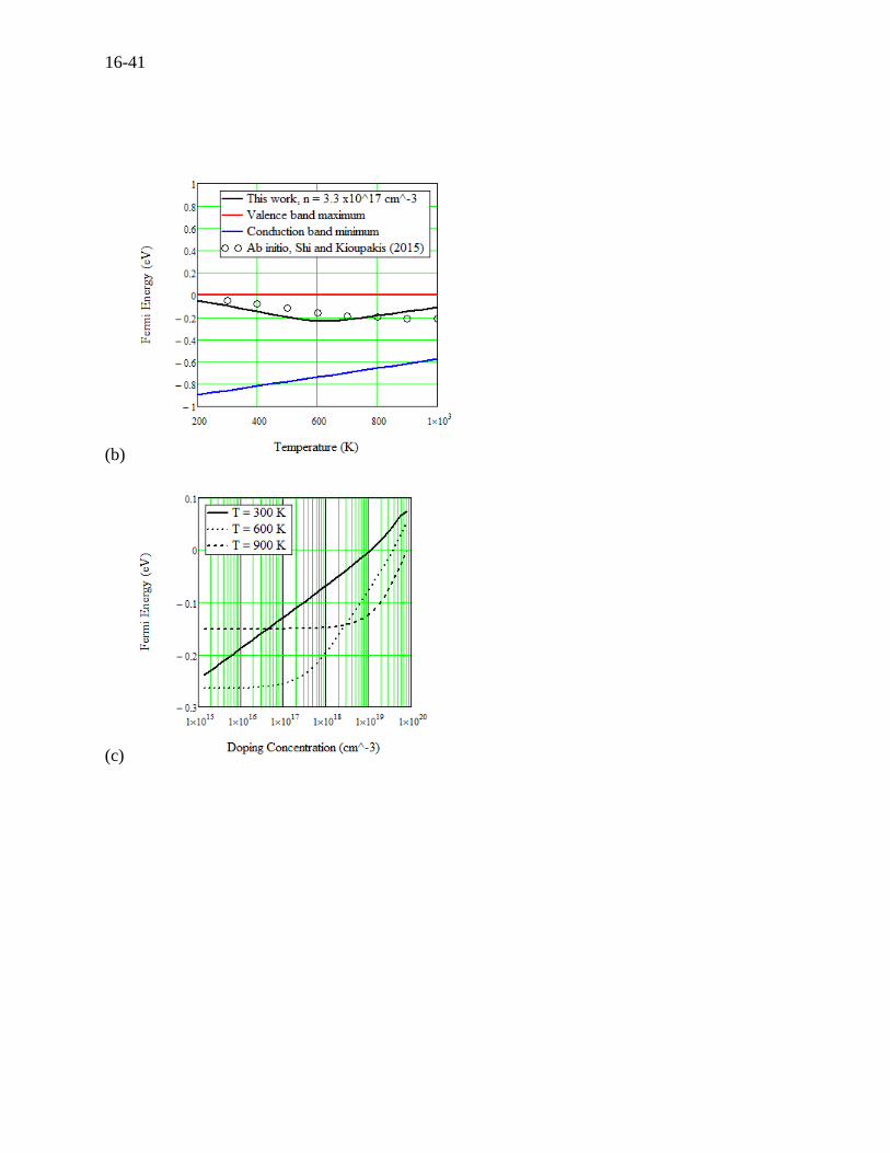
An attempt is made here to predict the TE transport properties for p-type SnSe using the present
model. The input data are shown in Table 16.1, where the values given from the literature have
the references but the values without references are estimations in this work. The majority carrier
of p-type SnSe is holes. Since we could not find measured total DOS effective masses from
literature, we had to estimate them by fitting the measurements of concentration by Zhao
(2014)[28] as shown in Figure 16.14 (a). We obtained 0.65 mo for holes and 9.5 mo for electrons
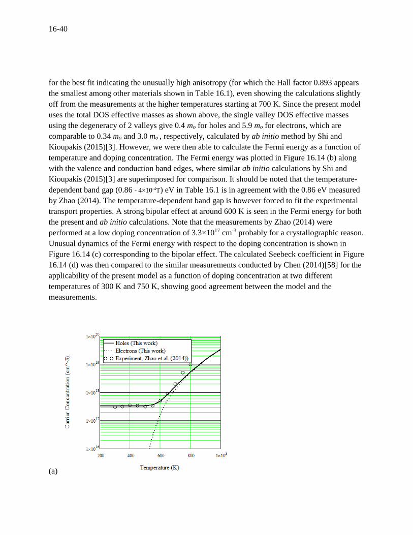
16-40
for the best fit indicating the unusually high anisotropy (for which the Hall factor 0.893 appears
the smallest among other materials shown in Table 16.1), even showing the calculations slightly
off from the measurements at the higher temperatures starting at 700 K. Since the present model
uses the total DOS effective masses as shown above, the single valley DOS effective masses
using the degeneracy of 2 valleys give 0.4 mo for holes and 5.9 mo for electrons, which are
comparable to 0.34 mo and 3.0 mo , respectively, calculated by ab initio method by Shi and
Kioupakis (2015)[3]. However, we were then able to calculate the Fermi energy as a function of
temperature and doping concentration. The Fermi energy was plotted in Figure 16.14 (b) along
with the valence and conduction band edges, where similar ab initio calculations by Shi and
Kioupakis (2015)[3] are superimposed for comparison. It should be noted that the temperature-
dependent band gap (0.86 - 4×10⁻⁴T) eV in Table 16.1 is in agreement with the 0.86 eV measured
by Zhao (2014). The temperature-dependent band gap is however forced to fit the experimental
transport properties. A strong bipolar effect at around 600 K is seen in the Fermi energy for both
the present and ab initio calculations. Note that the measurements by Zhao (2014) were
performed at a low doping concentration of 3.3×1017 cm-3 probably for a crystallographic reason.
Unusual dynamics of the Fermi energy with respect to the doping concentration is shown in
Figure 16.14 (c) corresponding to the bipolar effect. The calculated Seebeck coefficient in Figure
16.14 (d) was then compared to the similar measurements conducted by Chen (2014)[58] for the
applicability of the present model as a function of doping concentration at two different
temperatures of 300 K and 750 K, showing good agreement between the model and the
measurements.
(a)
16-41
(b)
(c)
16-42
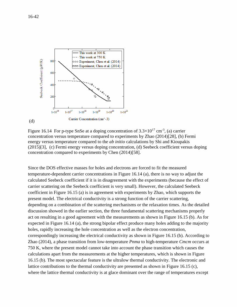
(d)
Figure 16.14 For p-type SnSe at a doping concentration of 3.3×1017 cm-3, (a) carrier
concentration versus temperature compared to experiments by Zhao (2014)[28], (b) Fermi
energy versus temperature compared to the ab initio calculations by Shi and Kioupakis
(2015)[3], (c) Fermi energy versus doping concentration, (d) Seebeck coefficient versus doping
concentration compared to experiments by Chen (2014)[58].
Since the DOS effective masses for holes and electrons are forced to fit the measured
temperature-dependent carrier concentrations in Figure 16.14 (a), there is no way to adjust the
calculated Seebeck coefficient if it is in disagreement with the experiments (because the effect of
carrier scattering on the Seebeck coefficient is very small). However, the calculated Seebeck
coefficient in Figure 16.15 (a) is in agreement with experiments by Zhao, which supports the
present model. The electrical conductivity is a strong function of the carrier scattering,
depending on a combination of the scattering mechanisms or the relaxation times. As the detailed
discussion showed in the earlier section, the three fundamental scattering mechanisms properly
act on resulting in a good agreement with the measurements as shown in Figure 16.15 (b). As for
expected in Figure 16.14 (a), the strong bipolar effect produce many holes adding to the majority
holes, rapidly increasing the hole concentration as well as the electron concentration,
correspondingly increasing the electrical conductivity as shown in Figure 16.15 (b). According to
Zhao (2014), a phase transition from low-temperature Pnma to high-temperature Cmcm occurs at
750 K, where the present model cannot take into account the phase transition which causes the
calculations apart from the measurements at the higher temperatures, which is shown in Figure
16.15 (b). The most spectacular feature is the ultralow thermal conductivity. The electronic and
lattice contributions to the thermal conductivity are presented as shown in Figure 16.15 (c),
where the lattice thermal conductivity is at glace dominant over the range of temperatures except
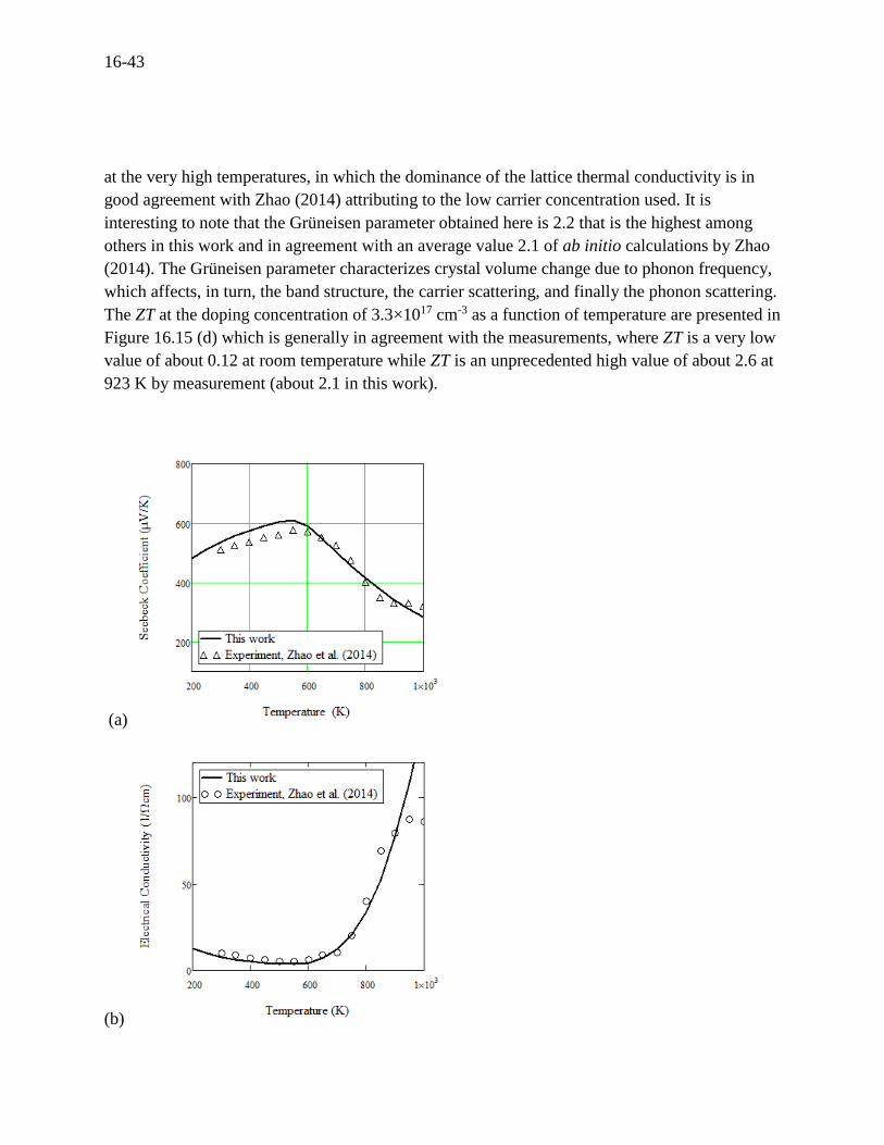
16-43
at the very high temperatures, in which the dominance of the lattice thermal conductivity is in
good agreement with Zhao (2014) attributing to the low carrier concentration used. It is
interesting to note that the Grüneisen parameter obtained here is 2.2 that is the highest among
others in this work and in agreement with an average value 2.1 of ab initio calculations by Zhao
(2014). The Grüneisen parameter characterizes crystal volume change due to phonon frequency,
which affects, in turn, the band structure, the carrier scattering, and finally the phonon scattering.
The ZT at the doping concentration of 3.3×1017 cm-3 as a function of temperature are presented in
Figure 16.15 (d) which is generally in agreement with the measurements, where ZT is a very low
value of about 0.12 at room temperature while ZT is an unprecedented high value of about 2.6 at
923 K by measurement (about 2.1 in this work).
(a)
(b)
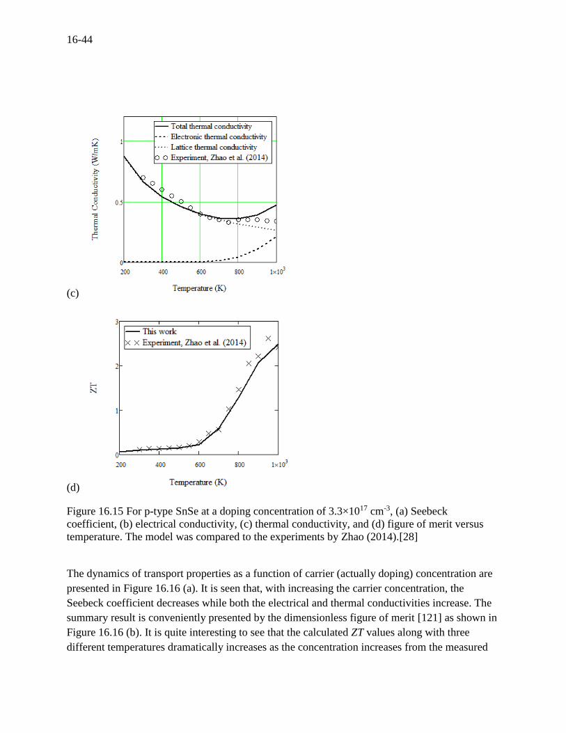
16-44
(c)
(d)
Figure 16.15 For p-type SnSe at a doping concentration of 3.3×1017 cm-3, (a) Seebeck
coefficient, (b) electrical conductivity, (c) thermal conductivity, and (d) figure of merit versus
temperature. The model was compared to the experiments by Zhao (2014).[28]
The dynamics of transport properties as a function of carrier (actually doping) concentration are
presented in Figure 16.16 (a). It is seen that, with increasing the carrier concentration, the
Seebeck coefficient decreases while both the electrical and thermal conductivities increase. The
summary result is conveniently presented by the dimensionless figure of merit [121] as shown in
Figure 16.16 (b). It is quite interesting to see that the calculated ZT values along with three
different temperatures dramatically increases as the concentration increases from the measured
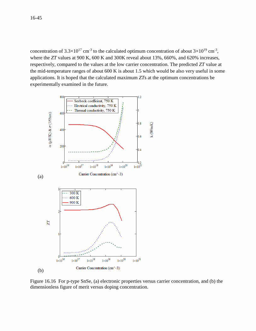
16-45
concentration of 3.3×1017 cm-3 to the calculated optimum concentration of about 3×1019 cm-3,
where the ZT values at 900 K, 600 K and 300K reveal about 13%, 660%, and 620% increases,
respectively, compared to the values at the low carrier concentration. The predicted ZT value at
the mid-temperature ranges of about 600 K is about 1.5 which would be also very useful in some
applications. It is hoped that the calculated maximum ZTs at the optimum concentrations be
experimentally examined in the future.
(a)
(b)
Figure 16.16 For p-type SnSe, (a) electronic properties versus carrier concentration, and (b) the
dimensionless figure of merit versus doping concentration.
16-46
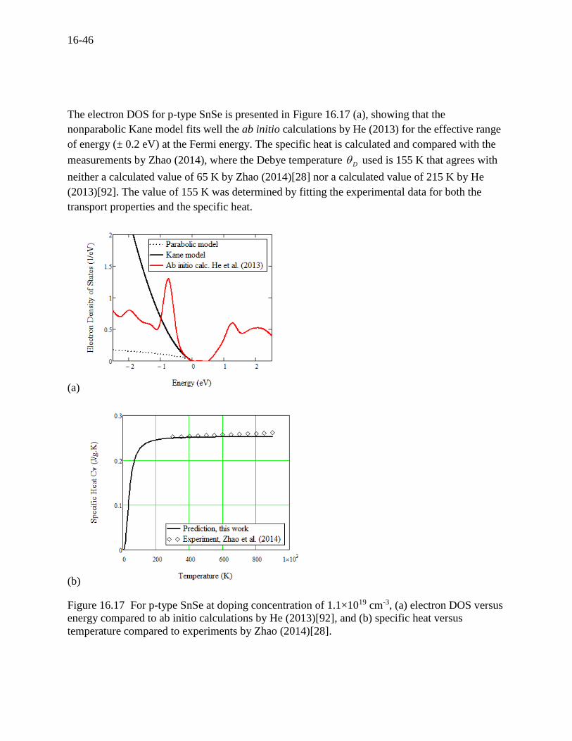
The electron DOS for p-type SnSe is presented in Figure 16.17 (a), showing that the
nonparabolic Kane model fits well the ab initio calculations by He (2013) for the effective range
of energy (± 0.2 eV) at the Fermi energy. The specific heat is calculated and compared with the
measurements by Zhao (2014), where the Debye temperature D used is 155 K that agrees with
neither a calculated value of 65 K by Zhao (2014)[28] nor a calculated value of 215 K by He
(2013)[92]. The value of 155 K was determined by fitting the experimental data for both the
transport properties and the specific heat.
(a)
(b)
Figure 16.17 For p-type SnSe at doping concentration of 1.1×1019 cm-3, (a) electron DOS versus
energy compared to ab initio calculations by He (2013)[92], and (b) specific heat versus
temperature compared to experiments by Zhao (2014)[28].
16-47
Transport Properties for n-type Si0.7Ge0.3
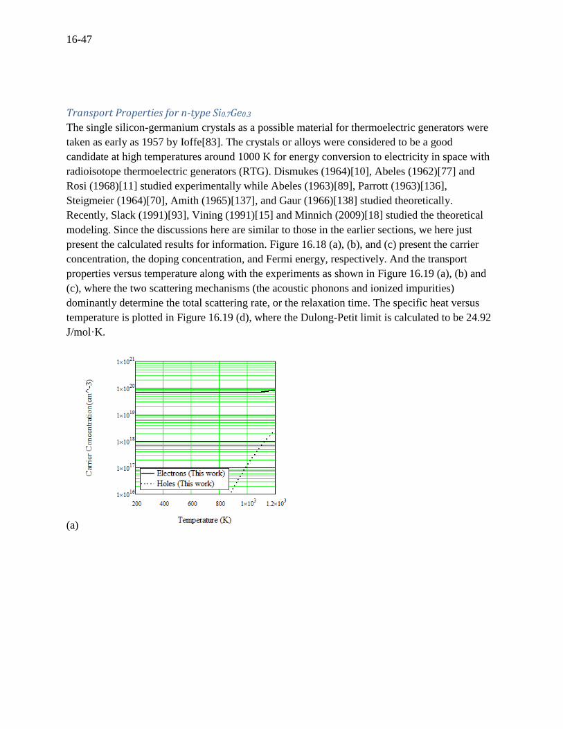
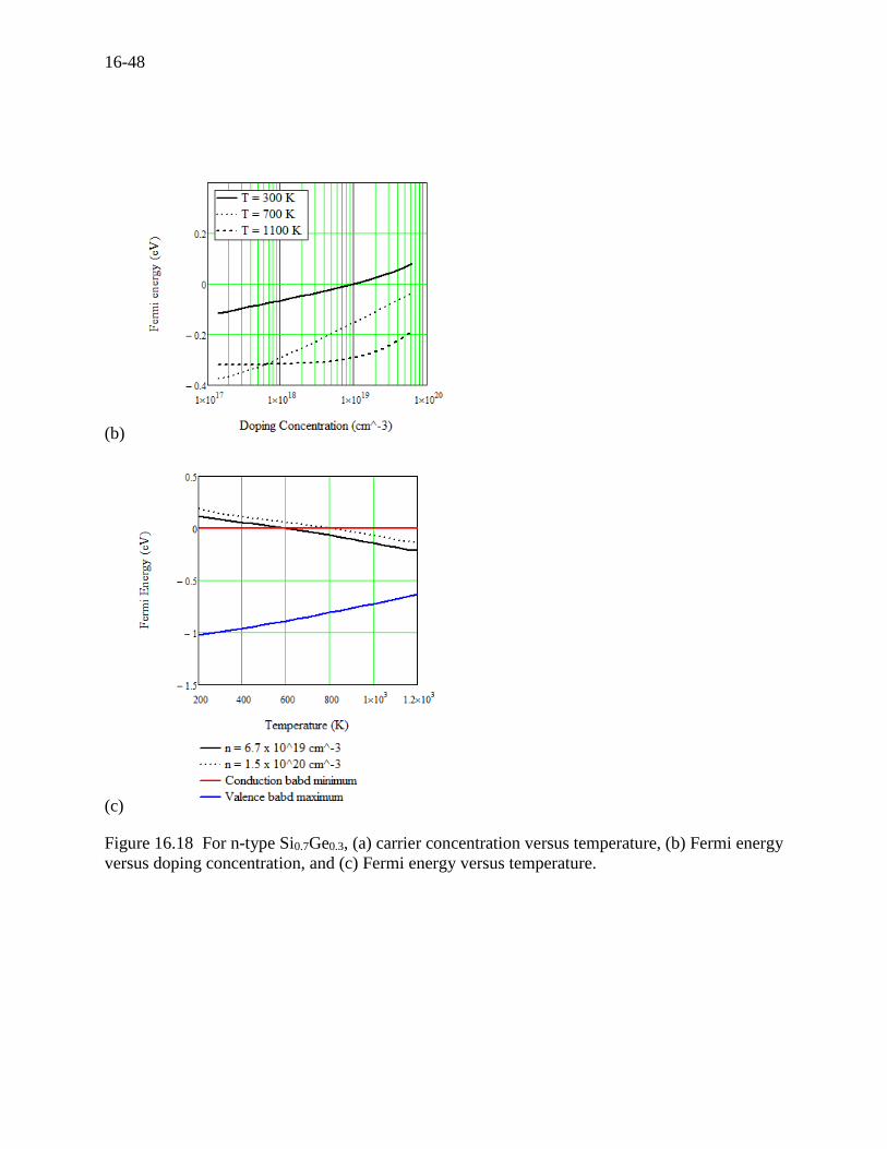
The single silicon-germanium crystals as a possible material for thermoelectric generators were
taken as early as 1957 by Ioffe[83]. The crystals or alloys were considered to be a good
candidate at high temperatures around 1000 K for energy conversion to electricity in space with
radioisotope thermoelectric generators (RTG). Dismukes (1964)[10], Abeles (1962)[77] and
Rosi (1968)[11] studied experimentally while Abeles (1963)[89], Parrott (1963)[136],
Steigmeier (1964)[70], Amith (1965)[137], and Gaur (1966)[138] studied theoretically.
Recently, Slack (1991)[93], Vining (1991)[15] and Minnich (2009)[18] studied the theoretical
modeling. Since the discussions here are similar to those in the earlier sections, we here just
present the calculated results for information. Figure 16.18 (a), (b), and (c) present the carrier
concentration, the doping concentration, and Fermi energy, respectively. And the transport
properties versus temperature along with the experiments as shown in Figure 16.19 (a), (b) and
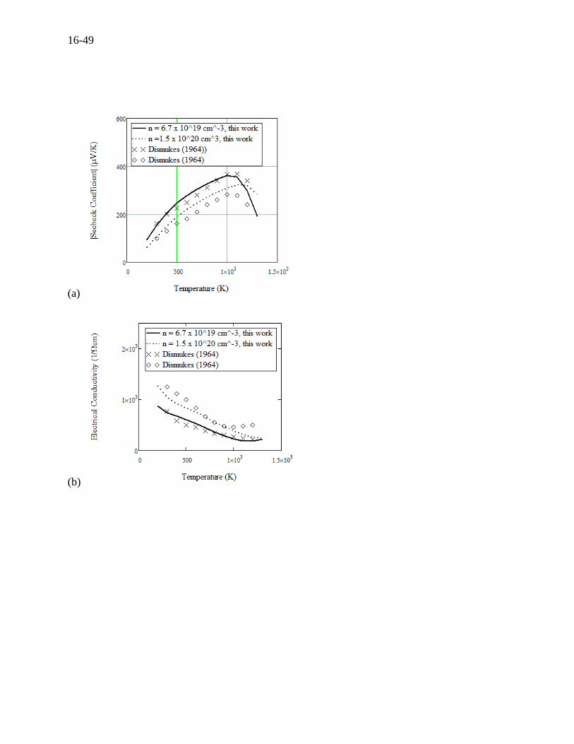
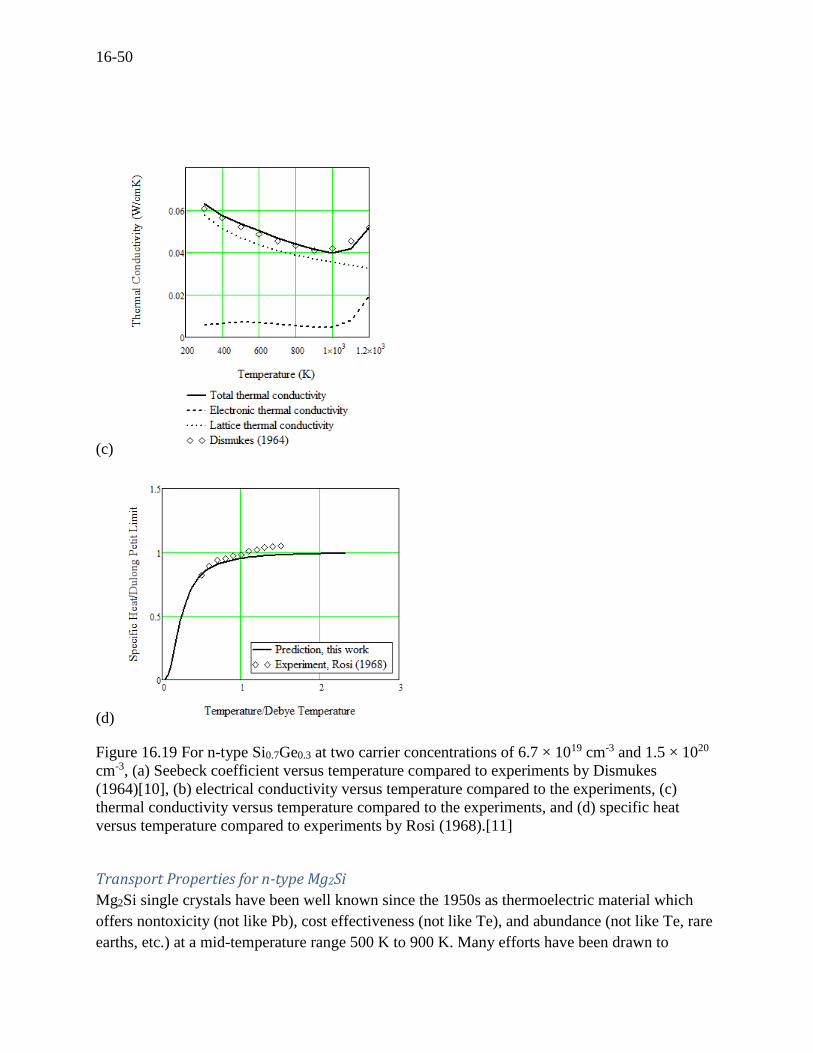
(c), where the two scattering mechanisms (the acoustic phonons and ionized impurities)
dominantly determine the total scattering rate, or the relaxation time. The specific heat versus
temperature is plotted in Figure 16.19 (d), where the Dulong-Petit limit is calculated to be 24.92
J/mol·K.
(a)
16-48
(b)
(c)
Figure 16.18 For n-type Si0.7Ge0.3, (a) carrier concentration versus temperature, (b) Fermi energy
versus doping concentration, and (c) Fermi energy versus temperature.
16-49
(a)
(b)
16-50
(c)
(d)
Figure 16.19 For n-type Si0.7Ge0.3 at two carrier concentrations of 6.7 × 1019 cm-3 and 1.5 × 10²⁰
cm-3, (a) Seebeck coefficient versus temperature compared to experiments by Dismukes
(1964)[10], (b) electrical conductivity versus temperature compared to the experiments, (c)
thermal conductivity versus temperature compared to the experiments, and (d) specific heat
versus temperature compared to experiments by Rosi (1968).[11]
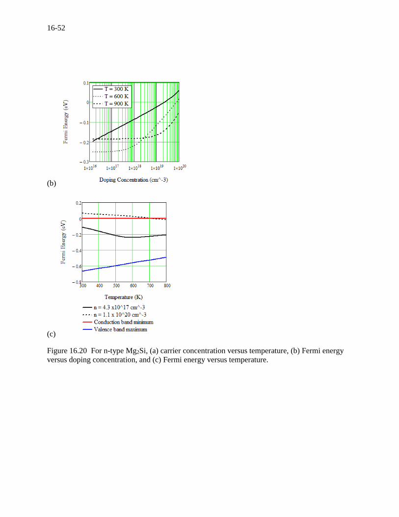
Transport Properties for n-type Mg2Si
Mg2Si single crystals have been well known since the 1950s as thermoelectric material which
offers nontoxicity (not like Pb), cost effectiveness (not like Te), and abundance (not like Te, rare
earths, etc.) at a mid-temperature range 500 K to 900 K. Many efforts have been drawn to
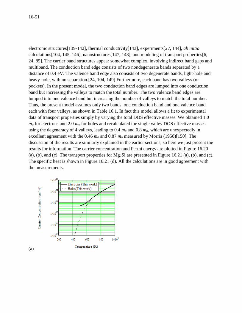
16-51
electronic structures[139-142], thermal conductivity[143], experiments[27, 144], ab initio
calculations[104, 145, 146], nanostructures[147, 148], and modeling of transport properties[6,
24, 85]. The carrier band structures appear somewhat complex, involving indirect band gaps and
multiband. The conduction band edge consists of two nondegenerate bands separated by a
distance of 0.4 eV. The valence band edge also consists of two degenerate bands, light-hole and
heavy-hole, with no separation.[24, 104, 149] Furthermore, each band has two valleys (or
pockets). In the present model, the two conduction band edges are lumped into one conduction
band but increasing the valleys to match the total number. The two valence band edges are
lumped into one valence band but increasing the number of valleys to match the total number.
Thus, the present model assumes only two bands, one conduction band and one valence band
each with four valleys, as shown in Table 16.1. In fact this model allows a fit to experimental
data of transport properties simply by varying the total DOS effective masses. We obtained 1.0
mo for electrons and 2.0 mo for holes and recalculated the single valley DOS effective masses
using the degeneracy of 4 valleys, leading to 0.4 mo and 0.8 mo, which are unexpectedly in
excellent agreement with the 0.46 mo and 0.87 mo measured by Morris (1958)[150]. The
discussion of the results are similarly explained in the earlier sections, so here we just present the
results for information. The carrier concentration and Fermi energy are plotted in Figure 16.20
(a), (b), and (c). The transport properties for Mg2Si are presented in Figure 16.21 (a), (b), and (c).
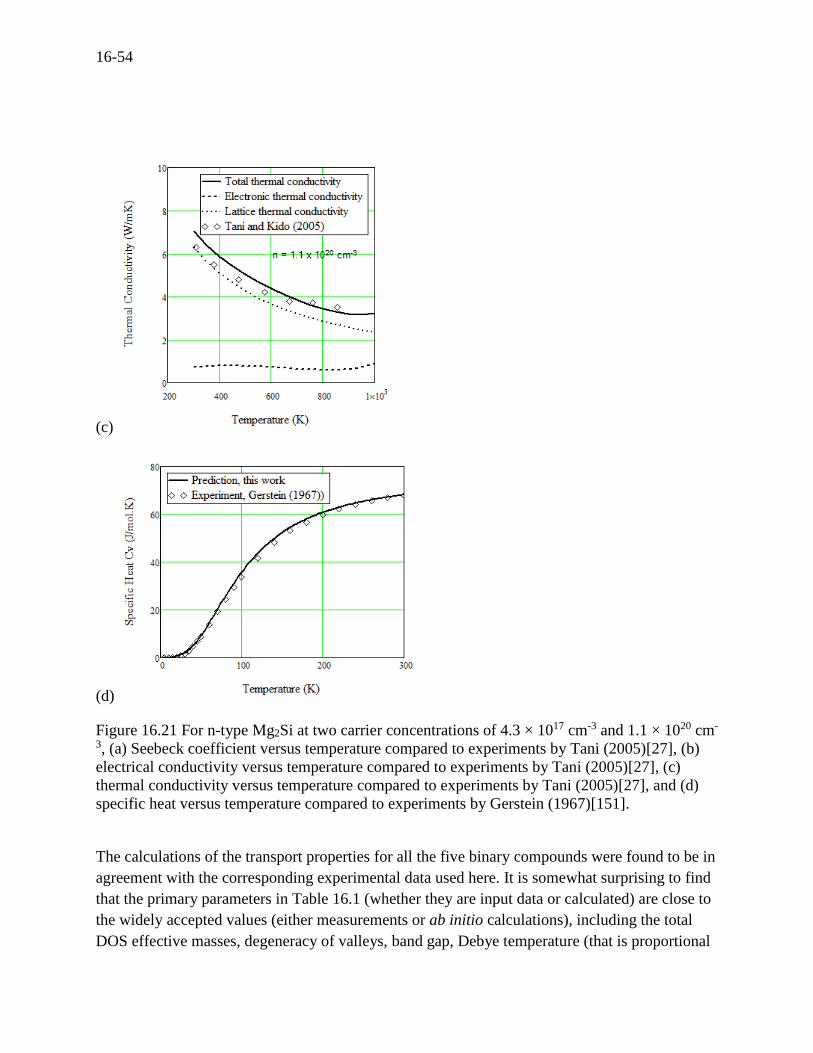
The specific heat is shown in Figure 16.21 (d). All the calculations are in good agreement with
the measurements.
(a)
16-52
(b)
(c)
Figure 16.20 For n-type Mg2Si, (a) carrier concentration versus temperature, (b) Fermi energy
versus doping concentration, and (c) Fermi energy versus temperature.
16-53
(a)
(b)
16-54
(c)
(d)
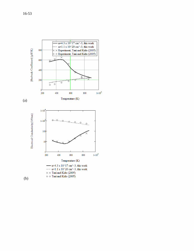
Figure 16.21 For n-type Mg2Si at two carrier concentrations of 4.3 × 1017 cm-3 and 1.1 × 1020 cm-
3, (a) Seebeck coefficient versus temperature compared to experiments by Tani (2005)[27], (b)
electrical conductivity versus temperature compared to experiments by Tani (2005)[27], (c)
thermal conductivity versus temperature compared to experiments by Tani (2005)[27], and (d)
specific heat versus temperature compared to experiments by Gerstein (1967)[151].
The calculations of the transport properties for all the five binary compounds were found to be in
agreement with the corresponding experimental data used here. It is somewhat surprising to find
that the primary parameters in Table 16.1 (whether they are input data or calculated) are close to
the widely accepted values (either measurements or ab initio calculations), including the total
DOS effective masses, degeneracy of valleys, band gap, Debye temperature (that is proportional
16-55
to the velocity of speed), and Grüneisen parameter. It is quite meaningful that the model is able
to precisely predict the experimental values with the realistic input data. However, we had to
vary the deformation potential to make it fit the measured electrical conductivity only in
magnitude, not in slope (the slope is associated with the electron scattering), which is a common
practice in modeling due to the usually unknown deformation potential. The most important
parameter is the DOS effective mass that affects almost all electronic parts of the model such as
the Fermi energy, carrier concentration, carrier density of states, electron scattering, transport
properties, etc. Firstly, the calculations of transport properties are in agreement with the
experiments. Then, the model can be said robust if the input values of the effective masses with
the degeneracy of valleys are in agreement with the measured effective masses because they
cannot simultaneously fit the various corresponding experimental values without the
combination of both the realistic input values and the right model. The second important
parameter is the Debye temperature which affects both the electronic and phonon parts of the
model: the velocity of sound, acoustic phonon scattering, electrical conductivity, electronic and
lattice thermal conductivity, point defects scattering, cutoff frequency, phonon DOS, and specific
heat. The present model differs from other typical models in that the velocity of sound is taken
from the literature and hence the Debye temperature affects only the lattice thermal conductivity
(the specific heat is not usually included). The Debye temperature is typically experimentally
determined from the specific heat measured at low temperatures. Hence only the Grüneisen
parameter of the Umklapp processes allows to adjust the magnitude of the lattice thermal
conductivity. Lastly, if the two parameters (DOS effective mass and Debye temperature) are
close to the realistic values, the model can be said to be robust.
16.4 Summary
A theoretical model based on the linearized Boltzmann transport equation with the relaxation
time approximation and the Debye model has been developed incorporating nonparabolicity,
two-band (conduction and valence bands) Kane model, and Hall factor without the fitting
parameters. It calculates the thermoelectric transport properties (Seebeck coefficient, electrical
conductivity, and thermal conductivity) along with the Hall mobility, Fermi energy (as a function
of temperature and doping concentration), carrier concentration, electron and phonon density of
states, and specific heat. In particular, it provides electron relaxation times and electronic and
lattice contributions to the thermal conductivity including the bipolar effect. We found that the
present model is generally in good agreement with reported experiments for five thermoelectric
bulk materials (PbTe, Bi2Te3, SnSe, Si0.7Ge0.3, and Mg2Si). This theoretical model is important
for nanostructured materials in which the modelling is based on that of the bulk materials and ab
16-56
initio numerical calculations are intrinsically incapable of precisely predicting the experimental
values due to their inability to handle temperature-dependent band gap and effective masses.
The present model differs from others as follows: Firstly, the three modified electron scattering
mechanisms (acoustic phonons, polar optical phonons, and ionized impurities) are demonstrated
to be responsible for the electron relaxation times. Secondly, concomitant agreement between
input data, calculations, and experiments for the DOS effective masses, electron and hole
concentrations, velocity of sound (calculated rather than taken from literature), Seebeck
coefficient, electrical conductivity, electronic and lattice thermal conductivities, and Grüneisen
parameter. Since the present model uses no fitting of parameters, it is able to examine a recently
attracted material of SnSe, not only predicting the measured transport properties (the
unprecedented ZT value of 2.6 at 923 K), but also suggesting a significant improvement in ZT
value of about a 600 % increase (a ZT value of 1.5) at 600 K and an increased doping
concentration compared to the reported ZT value of 0.13 at that temperature.
REFERENCES
1. Rowe, D.M., CRC handbook of thermoelectrics. 1995, Boca Raton London New York: CRC Press.
2. Rowe, D.M., Thermoelectrics handbook; macro to nano. 2006, Roca Raton: CRC Taylor & Francis,.
3. Shi, G. and E. Kioupakis, Quasiparticle band structures and thermoelectric transport properties of p-type SnSe. Journal of Applied Physics, 2015. 117(6): p. 065103.
4. Hicks, L. and M. Dresselhaus, Effect of quantum-well structures on the thermoelectric figure of merit. Physical Review B, 1993. 47(19): p. 12727-12731.
5. Harman, T.C., D.L. Spears, and M.J. Manfra, High thermoelecrtic figures of merit in PbTe Quantum wells. Journal of Electronic Materials, 1996. 25(7): p. 1121-1127.
6. Zhou, J., et al., Semiclassical model for thermoelectric transport in nanocomposites. Physical Review B, 2010. 82(11).
7. Debye, P. and E. Conwell, Electrical Properties of N-Type Germanium. Physical Review, 1954. 93(4): p. 693-706.
8. Herring, C. and E. Vogt, Transport and Deformation-Potential Theory for Many-Valley Semiconductors with Anisotropic Scattering. Physical Review, 1956. 101(3): p. 944-961.
9. Chasmar, R.P. and R. Stratton, The thermoelectric figure of merit and its relation to thermoelectric generators. J. Electron. Control., 1959. 7: p. 52-72.
10. Dismukes, J.P., et al., Thermal and Electrical Properties of Heavily Doped Ge-Si Alloys up to 1300°K. Journal of Applied Physics, 1964. 35(10): p. 2899.
16-57
11. Rosi, F.D., Thermoelectricity and thermoelectric power generation. Solid State Electronics, 1968. 11: p. 833-868.
12. Ravich, Y.I., B.A. Efimova, and I.A. Smirnov, Semiconducting Lead Chalcogenides. 1970, New York: Plenum Press.
13. Ravich, Y.I., B.A. Efimova, and V.I. Tamabohenko, Scattering of current carriers and transport phenomena in lead chalcogenides II Experiment. Phys. Stat. Sol., 1971. (b) 43: p. 453-469.
14. Harris, J.J. and B.K. Ridley, Room temperature transport properties of p-type PbTe. J. Phys. Chem. Solids, 1972. 33: p. 1455-1464.
15. Vining, C.B., A model for the high-temperature transport properties of heavily doped n-type silicon-germanium alloys. Journal of Applied Physics, 1991. 69(1): p. 331.
16. Lundstrom, M., Fundamentals of carrier transport, 2nd ed. 2000, Cambridge: Cambridge University Press.
17. Minnich, A. and G. Chen, Modified effective medium formulation for the thermal conductivity of nanocomposites. Applied Physics Letters, 2007. 91(7): p. 073105.
18. Minnich, A., et al., Modeling study of thermoelectric SiGe nanocomposites. Physical Review B, 2009. 80(15).
19. Chen, G., Nanoscale energy transport and conversion. Mechanical Engineering. 2005: OXFORD University Press. 531.
20. Vineis, C., et al., Carrier concentration and temperature dependence of the electronic transport properties of epitaxial PbTe and PbTe/PbSe nanodot superlattices. Physical Review B, 2008. 77(23).
21. Youn, S. and A. Freeman, First-principles electronic structure and its relation to thermoelectric properties of Bi2Te3. Physical Review B, 2001. 63(8).
22. Kim, M., A. Freeman, and C. Geller, Screened exchange LDA determination of the ground and excited state properties of thermoelectrics: Bi2Te3. Physical Review B, 2005. 72(3).
23. Bilc, D., S. Mahanti, and M. Kanatzidis, Electronic transport properties of PbTe and AgPbmSbTe2+m systems. Physical Review B, 2006. 74(12).
24. Bahk, J.-H., Z. Bian, and A. Shakouri, Electron transport modeling and energy filtering for efficient thermoelectric <span class="aps-inline-formula"><math><msub><mtext>Mg</mtext><mn>2</mn></msub><msub><mrow><mtext>Si</mtext></mrow><mrow><mn>1</mn><mtext>−</mtext><mi>x</mi></mrow></msub><msub><mtext>Sn</mtext><mi>x</mi></msub></math></span> solid solutions. Physical Review B, 2014. 89(7).
25. Jeon, H.-W., et al., Electrical and thermoelectrical properties of undoped Bi2Te3-SbeTe3 and Bi2Te3-Sb2Te3-Sb2Se3 single crystals. J. Phys. Chem. Solids, 1991. 52(4): p. 579-585.
26. Pei, Y., et al., Low effective mass leading to high thermoelectric performance. Energy & Environmental Science, 2012. 5(7): p. 7963.
27. Tani, J.-i. and H. Kido, Thermoelectric properties of Bi-doped Mg2Si semiconductors. Physica B: Condensed Matter, 2005. 364(1-4): p. 218-224.
16-58
28. Zhao, L.D., et al., Ultralow thermal conductivity and high thermoelectric figure of merit in SnSe crystals. Nature, 2014. 508(7496): p. 373-7.
29. Wilson, A.H., The theory of metals, 2nd ed. 1953, Cambridge: Cambridge University Press.
30. Ziman, J.M., Electrons and phonons. 1960, London: Oxford University Press. 31. Callaway, J., Model for Lattice Thermal Conductivity at Low Temperatures. Physical
Review, 1959. 113(4): p. 1046-1051. 32. Holland, M., Analysis of Lattice Thermal Conductivity. Physical Review, 1963. 132(6): p.
2461-2471. 33. Herring, C., Transport properties of a many-vally semiconductor. The Bell System
Technical Journal, 1955. 34(2): p. 237-290. 34. Kane, E.O., Semiconductors and semimetals, Chapter 3 The k-p method. 1966, New York:
Academic Press. 35. Putley, E.H., The Hall Effect and Related Phenomena. Semi-conductorMonographs. 1960,
London: Butterworths. 36. Abeles, B. and S. Meiboom, Theory of the Galvanomagnetic Effects in Germanium.
Physical Review, 1954. 95(1): p. 31-37. 37. Shibuya, M., Magnetoresistance Effect in Cubic Semiconductors with Spheroidal Energy
Surfaces. Physical Review, 1954. 95(6): p. 1385-1393. 38. Heremans, J., C. Thrush, and D. Morelli, Thermopower enhancement in lead telluride
nanostructures. Physical Review B, 2004. 70(11). 39. Goldsmid, H.J., Thermoelectric Refrigeration. 1964, New York: Plenum Press. 240. 40. Nolas, G.S., J. Sharp, and H.J. Goldsmid, Thermoelectrics: basic principles and new
materials developments. 2001, Berlin: Springer,. 41. Mott, N.F. and H. Jones, The theory of the properties of metals and alloys. 1958, New
York: Dover Publications, Inc.,. 42. Heremans, J.P., B. Wiendlocha, and A.M. Chamoire, Resonant levels in bulk
thermoelectric semiconductors. Energy & Environmental Science, 2012. 5(2): p. 5510. 43. Bardeen, J. and W. Shockley, Deformation Potentials and Mobilities in Non-Polar
Crystals. Physical Review, 1950. 80(1): p. 72-80. 44. Brooks, H., Scattering by ionized impurities in semiconductors. Phys. Rev., 1951. 83: p.
879. 45. Howarth, D.J. and E.H. Sondheimer, The theory of electronic conductionin polar semi-
conductors. Proc. Roy. Soc. London, 1953. A 219: p. 53. 46. Ehrenreich, H., Electric scattering in InSb. J. Phys. Chem. Solids, 1957. 2: p. 131-149. 47. Ehrenreich, H., Band Structure and Transport Properties of Some 3–5 Compounds.
Journal of Applied Physics, 1961. 32(10): p. 2155. 48. Ravich, Y.I., B.A. Efimova, and V.I. Tamabohenko, Scattering of current carriers and
transport phenomena in lead chalcogenides. Phys. Stat. Sol., 1971. (b) 43: p. 11-33. 49. Nag, B.R., Electron Transport in Compound Semiconductors. Springer Series in Solid
Sciences. 1980, New York: Springer.
16-59
50. Zayachuk, D.M., The dominant mechanisms of charge-carrier scattering in lead telluride. Semiconductors, 1997. 31: p. 173.
51. Freik, D.M., L.I. Nykyruy, and V.M. Shperun, Scattering mechanisms of electrons in monocrystalline PbTe, PbSe and PbS. Semicond. phys. Quantum Electron and Optoelectron., 2002. 5(4): p. 362-367.
52. Huang, B.-L. and M. Kaviany, Ab initio and molecular dynamics predictions for electron and phonon transport in bismuth telluride. Physical Review B, 2008. 77: p. 125209.
53. Ahmad, S. and S.D. Mahanti, Energy and temperature dependence of relaxation time and Wiedemann-Franz law on PbTe. Physical Review B, 2010. 81(16).
54. Broido, D.A. and T.L. Reinecke, Thermoelectric transport in quantum well superlattices. Applied Physics Letters, 1997. 70(21): p. 2834.
55. Kolodziejczak, J., On the scattering processes in semiconductors. Phys. Stat. Sol., 1967. 19: p. 231.
56. Amith, A., I. Kudman, and E. Steigmeier, Electron and Phonon Scattering in GaAs at High Temperatures. Physical Review, 1965. 138(4A): p. A1270-A1276.
57. Bux, S.K., et al., Mechanochemical synthesis and thermoelectric properties of high quality magnesium silicide. Journal of Materials Chemistry, 2011. 21(33): p. 12259.
58. Chen, C.-L., et al., Thermoelectric properties of p-type polycrystalline SnSe doped with Ag. Journal of Materials Chemistry A, 2014. 2(29): p. 11171.
59. Rogers, L.M., The Hall mobility and thermoelectric power of p-type lead telluride. Brit. J. Appl. Phys., 1967. 18: p. 1227-1235.
60. Androulakis, J., et al., High-temperature thermoelectric properties of n-type PbSe doped with Ga, In, and Pb. Physical Review B, 2011. 83(19).
61. Chi, H., et al., Low-temperature transport properties of Tl-doped Bi_{2}Te_{3} single crystals. Physical Review B, 2013. 88(4).
62. Debye, P., The theory of specific heats. Ann. Phys. Lpz. (4), 1912. 39: p. 798. 63. Callen, H., Electric Breakdown in Ionic Crystals. Physical Review, 1949. 76(9): p. 1394-
1402. 64. Conwell, E. and V. Weisskopf, Theory of Impurity Scattering in Semiconductors. Physical
Review, 1950. 77(3): p. 388-390. 65. Blatt, F.J., Theory of mobility of electrons in solids, in Solid State Physics, F. Seitz and D.
Turnbull, Editors. 1957, Academic Press: New York. 66. Chattopadhyay, D. and H. Queisser, Electron scattering by ionized impurities in
semiconductors. Reviews of Modern Physics, 1981. 53(4): p. 745-768. 67. Herring, C., Role of Low-Energy Phonons in Thermal Conduction. Physical Review, 1954.
95(4): p. 954-965. 68. Klemens, P.G., The scattering of low-frequency lattice wavesby static imperfections.
Proc. Phys. Soc., 1955. 68(12): p. 1113-1128. 69. Ziman, J.M., The effect of free electrons in lattice conduction. The Philosophical
Magazine, 1956. 1(2): p. 191-198.
16-60
70. Steigmeier, E. and B. Abeles, Scattering of Phonons by Electrons in Germanium-Silicon Alloys. Physical Review, 1964. 136(4A): p. A1149-A1155.
71. Berman, R., Thermal conduction in solids. 1976, Oxford: Clarendon Press. 72. Leibfried, G. and E. Schlomann, Warmeleitung in elektrisch isolierenden Kristallen.
Nachrichten der Akademie der Wissenschaften in Gottingen, lia, Mathematisch-Physikalische Klasse, 1954: p. 71-93.
73. Ziman, J.M., The effect of free electrons in lattice conduction II. The Philosophical Magazine, 1956. 2(14): p. 292-.
74. Goldsmid, H.J., Heat conduction in bismuth telluride. Proc. Phys. Soc., 1958. 72: p. 17. 75. Klemens, P., Thermal Resistance due to Point Defects at High Temperatures. Physical
Review, 1960. 119(2): p. 507-509. 76. Slack, G. and C. Glassbrenner, Thermal Conductivity of Germanium from 3°K to 1020°K.
Physical Review, 1960. 120(3): p. 782-789. 77. Abeles, B., et al., Thermal Conductivity of Ge-Si Alloys at High Temperatures. Physical
Review, 1962. 125(1): p. 44-46. 78. Holland, M., Phonon Scattering in Semiconductors From Thermal Conductivity Studies.
Physical Review, 1964. 134(2A): p. A471-A480. 79. Alekseeva, G.T., et al., Thermal conductivity of solid solutions based on lead telluride.
Sov. Phys. Semicond., 1971. 4(7): p. 1122-1125. 80. Parrott, J.E., Heat conduction mechanisms in semiconducting materials. Rev. int. hautes
Temper. Refract. Fr., 1979. 16: p. 393-403. 81. Klemens, P.G., Thermal conductivity and lattice vibrational modes. Solid StatePhysics
Chapter 7. 1958, New York: Academic Press Inc. 82. Ashcroft, N.W. and N.D. Mermin, Solid state physics. 1976, New York: Holt, Rinehart and
Winston. 83. Ioffe, A.F., Semiconductor thermoelement and thermoelectric cooling. 1957, London:
Infosearch Limited. 184. 84. Huang, B., et al., Low-temperature characterization and micropatterning of
coevaporated Bi[sub 2]Te[sub 3] and Sb[sub 2]Te[sub 3] films. Journal of Applied Physics, 2008. 104(11): p. 113710.
85. Satyala, N. and D. Vashaee, Modeling of Thermoelectric Properties of Magnesium Silicide (Mg2Si). Journal of Electronic Materials, 2012. 41(6): p. 1785-1791.
86. Tani, J.-i. and H. Kido, Thermoelectric properties of Al-doped Mg2Si1−xSnx (x≦0.1). Journal of Alloys and Compounds, 2008. 466(1-2): p. 335-340.
87. Kittel, C., Introduction-to-Solid-State-Physics 8th Edition. 2005: Wiley. 88. Madelung, O., Numerical Data and Functional Relationships in Science and Technology,
Group III: Crystal and Solid Physics, . Vol. 17 Semiconductors. 1983, Verlag Berlin: Springer.
89. Abeles, B., Lattice Thermal Conductivity of Disordered Semiconductor Alloys at High Temperatures. Physical Review, 1963. 131(5): p. 1906-1911.
16-61
90. Lyden, H., Temperature Dependence of the Effective Masses in PbTe. Physical Review, 1964. 135(2A): p. A514-A521.
91. Kohler, H., Non-parabolic E relation of the lowest conduction band in Bi2Te3. Phys. Stat. Sol., 1976. (b) 73: p. 95-104.
92. He, X., et al., The mechanical and thermo-physical properties and electronic structures of SnS and SnSe in orthorhombic structure. Journal of Alloys and Compounds, 2013. 556: p. 86-93.
93. Slack, G.A. and M.A. Hussain, The maximum possible conversion efficiency of silicon-germanium thermoelectric generators. Journal of Applied Physics, 1991. 70(5): p. 2694.
94. Fischetti, M. and S. Laux, Monte Carlo study of electron transport in silicon inversion layers. Physical Review B, 1993. 48(4): p. 2244-2274.
95. Pankratov, O.A. and P.P. Povarov, Charge states of vacancies in IV-VI semiconductors. Solid State Communications, 1988. 66(8): p. 847-853.
96. Parkinson, D.H. and J.E. Quarrington, The molar heats of lead sulphide selenide and telluride in the temperature range 20 K to 260 K. Proc. Phys. Soc., 1954. 67: p. 569.
97. Allgaier, R. and W. Scanlon, Mobility of Electrons and Holes in PbS, PbSe, and PbTe between Room Temperature and 4.2°K. Physical Review, 1958. 111(4): p. 1029-1037.
98. Allgaier, R.S., Valence Bands in Lead Telluride. Journal of Applied Physics, 1961. 32(10): p. 2185.
99. Cochran, W., et al., The crystal dynamics of lead telluride. Proc. Roy. Soc. London, 1966. 293(1435): p. 433-451.
100. Wright, D.A., Materials for direct-conversion thermoelectric generators. Metallurgical Reviews, 1970: p. 147-160.
101. Tsang, Y. and M. Cohen, Calculation of the Temperature Dependence of the Energy Gaps in PbTe and SnTe. Physical Review B, 1971. 3(4): p. 1254-1261.
102. Crocker, A.J. and L.M. Rogers, Interpretation of the hall coefficient electrical resistivity and Seebeck coefficient of p-type lead telluride. Brit. J. Appl. Phys., 1967. 18: p. 563-573.
103. Martinez, G., M. Schlüter, and M. Cohen, Electronic structure of PbSe and PbTe II. Optical properties. Physical Review B, 1975. 11(2): p. 660-670.
104. Boulet, P., et al., Electronic properties of the Mg2Si thermoelectric material investigated by linear-response density-functional theory. Computational Materials Science, 2011. 50(3): p. 847-851.
105. Zhang, Y., et al., Thermodynamic properties of PbTe, PbSe, and PbS: First-principles study. Physical Review B, 2009. 80(2).
106. Tian, Z., et al., On the importance of optical phonons to thermal conductivity in nanostructures. Applied Physics Letters, 2011. 99(5): p. 053122.
107. Tian, Z., et al., Phonon conduction in PbSe, PbTe, and PbTe_{1−x}Se_{x} from first-principles calculations. Physical Review B, 2012. 85(18).
108. Wang, B.-T. and P. Zhang, Phonon spectrum and bonding properties of Bi2Se3: Role of strong spin-orbit interaction. Applied Physics Letters, 2012. 100(8): p. 082109.
16-62
109. Bilc, D., et al., Resonant States in the Electronic Structure of the High Performance Thermoelectrics AgPbmSbTe2+m: The Role of Ag-Sb Microstructures. Physical Review Letters, 2004. 93(14).
110. Martinez, G., M. Schlüter, and M. Cohen, Electronic structure of PbSe and PbTe. I. Band structures, densities of states, and effective masses. Physical Review B, 1975. 11(2): p. 651-659.
111. Shiga, T., et al., Microscopic mechanism of low thermal conductivity in lead telluride. Physical Review B, 2012. 85(15).
112. Steigmeier, E.F., The Debye Temperatures of Iii-V Compounds. Applied Physics Letters, 1963. 3(1): p. 6.
113. Goldsmid, H.J. and R.W. Douglas, The use of semiconductors in thermoelectric refrigeration. British Journal of Applied Physics, 1954. 5: p. 386-390.
114. Harman, T.C., et al., Preparation and some physical properties of Bi2Te3 Sb2Te3 and As2Te3. J. Phys. Chem. Solids, 1957. 2: p. 181-190.
115. Drabble, J.R. and C.H.L. Goodman, Chemical bonding in bismuth telluride. J. Phys. Chem. Solids, 1958. 5: p. 142-144.
116. Kohler, H., Non-parabolicity of the highest valence band of Bi2Te3 from Shubnikov-de Haas Effect. Phys. Stat. Sol., 1976. (b) 74: p. 591-600.
117. Park, M.S., et al., Electronic structure and volume effect on thermoelectric transport inp-type Bi and Sb tellurides. Physical Review B, 2010. 81(15).
118. Jenkins, J., J. Rayne, and R. Ure, Elastic Moduli and Phonon Properties of Bi_{2} Te_{3}. Physical Review B, 1972. 5(8): p. 3171-3184.
119. Mishra, S.K., S. Satpathy, and O. Jepsen, Electronic structure and thermoelectric properties of bithmuth telluride and bismuth selenide. J. Phys. Condens. Matter, 1997. 9: p. 461-470.
120. Larson, P., S.D. Mahanti, and M.G. Kanatzidis, Electronic structure and transport of Bi2Te3and BaBiTe3. Physical Review B, 2000. 61(12): p. 8162-8171.
121. Merkisz, J., et al., The Analysis of Exhaust Gas Thermal Energy Recovery Through a TEG Generator in City Traffic Conditions Reproduced on a Dynamic Engine Test Bed. Journal of Electronic Materials, 2014.
122. Rauh, H., et al., Generalised phonon density of states of the layer compounds Bi2Se3 Bi2Te3 Sb2Te3 and Bi2(Te05Se05)3. J. Phys. C: Solid State Phys., 1981. 14: p. 2705-2712.
123. Bessas, D., et al., Lattice dynamics in Bi_{2}Te_{3} and Sb_{2}Te_{3}: Te and Sb density of phonon states. Physical Review B, 2012. 86(22).
124. Wasscher, J.D., W. Albers, and C. Haas, Simple evaluation of the maximum thermoelectric figure of merit with application to mixed crystals SnS(1-x)Sex. Solid-State Electronics Bergamon Press, 1963. 6: p. 261-264.
125. Adouby, K., C. Perez-Vicente, and J.C. Jumas, Structure and temperature transformation of SnSe. Stabilization of a new cubic phase Sn4Bi2Se7. Z. Kristallogr., 1998. 213: p. 343-349.
16-63
126. Nariya, B.B., et al., Electrical transport properties of SnS and SnSe single crystals grown by direct vapor transport technique. Chalcogenide Letters, 2009. 6(10): p. 549-554.
127. Banik, A. and K. Biswas, Lead-free thermoelectrics: promising thermoelectric performance in p-type SnTe1−xSex system. Journal of Materials Chemistry A, 2014. 2(25): p. 9620.
128. Sassi, S., et al., Assessment of the thermoelectric performance of polycrystalline p-type SnSe. Applied Physics Letters, 2014. 104(21): p. 212105.
129. Han, Y.-M., et al., Thermoelectric performance of SnS and SnS–SnSe solid solution. J. Mater. Chem. A, 2015. 3(8): p. 4555-4559.
130. Au-Yang, M. and M. Cohen, Electronic Structure and Optical Properties of SnS2 and SnSe2. Physical Review, 1969. 178(3): p. 1279-1283.
131. Car, R., G. Ciucci, and L. Quartapelle, Electronic band structure of SnSe. Phys. Stat. Sol. (b), 1978. 86: p. 471.
132. Makinistian, L. and E.A. Albanesi, On the band gap location and core spectra of orthorhombic IV-VI compounds SnS and SnSe. physica status solidi (b), 2009. 246(1): p. 183-191.
133. Chen, S., K. Cai, and W. Zhao, The effect of Te doping on the electronic structure and thermoelectric properties of SnSe. Physica B: Condensed Matter, 2012. 407(21): p. 4154-4159.
134. Sun, Y., et al., Rocksalt SnS and SnSe: Native topological crystalline insulators. Physical Review B, 2013. 88(23).
135. Carrete, J., N. Mingo, and S. Curtarolo, Low thermal conductivity and triaxial phononic anisotropy of SnSe. Applied Physics Letters, 2014. 105(10): p. 101907.
136. Parrott, J.E., The high temperature thermal conductivity of semiconductor alloys. Proc. Phys. Soc., 1963. 81: p. 726-735.
137. Amith, A., Seebeck Coefficient in N-Type Germanium-Silicon Alloys: "Competition" Region. Physical Review, 1965. 139(5A): p. A1624-A1627.
138. Gaur, N., C. Bhandari, and G. Verma, Temperature Dependence of Density-of-States Effective Mass and the Electronic and Phonon Contributions to Thermal Resistance of Doped Si-Ge Alloys at High Temperatures. Physical Review, 1966. 144(2): p. 628-641.
139. Koenig, P., D.W. Lynch, and G.C. Danielson, Infrared absorption in magnesium silicide and Magnedium germanide. J. Phys. Chem. Solids, 1961. 20(1/2): p. 122-126.
140. Lee, P., Electronic Structure of Magnesium Silicide and Magnesium Germanide. Physical Review, 1964. 135(4A): p. A1110-A1114.
141. Au-Yang, M. and M. Cohen, Electronic Structure and Optical Properties of Mg2Si, Mg2Ge, and Mg2Sn. Physical Review, 1969. 178(3): p. 1358-1364.
142. Krivosheeva, A.V., et al., Band structure of Mg2Si and Mg2Ge semiconducting compounds with a strained crystal lattice. Semiconductors, 2002. 36(5): p. 496-500.
143. Martin, J.J., Thermal conductivity of Mg2Si, Mg2Ge and Mg2Sn. J. Phys. Chem. Solids, 1972. 33: p. 1139-1148.
16-64
144. Akasaka, M., et al., Composition dependent thermoelectric properties of sintered Mg2Si1−xGex (x=0 to 1) initiated from a melt-grown polycrystalline source. Thin Solid Films, 2007. 515(22): p. 8237-8241.
145. Wang, H., et al., Thermodynamic properties of Mg2Si and Mg2Ge investigated by first principles method. Journal of Alloys and Compounds, 2010. 499(1): p. 68-74.
146. Kutorasiński, K., J. Tobola, and S. Kaprzyk, Calculating electron transport coefficients of disordered alloys using the KKR-CPA method and Boltzmann approach: Application to Mg2Si1−xSnxthermoelectrics. Physical Review B, 2013. 87(19).
147. Zhang, X., et al., Enhanced thermoelectric performance of Mg2Si0.4Sn0.6 solid solutions by in nanostructures and minute Bi-doping. Applied Physics Letters, 2013. 103(6): p. 063901.
148. Farahi, N., et al., Sb- and Bi-doped Mg2Si: location of the dopants, micro- and nanostructures, electronic structures and thermoelectric properties. Dalton Trans, 2014. 43(40): p. 14983-91.
149. Zaitsev, V., et al., Highly effective Mg2Si1−xSnx thermoelectrics. Physical Review B, 2006. 74(4).
150. Morris, R., R. Redin, and G. Danielson, Semiconducting Properties of Mg2Si Single Crystals. Physical Review, 1958. 109(6): p. 1909-1915.
151. Gerstein, B.C., Thermal Study of Groups II—IV Semiconductors. Lattice Heat Capacities and Free Energies of Formation. Heat Capacity of Mg2Si from 15°—300°K. The Journal of Chemical Physics, 1967. 47(6): p. 2109.
16-65
Problems
16.1. Derive Equation (16.2) (see Chapter 11).
16.2. Explain the difference between the Hall carrier concentration and the carrier concentration.
16.3. Briefly explain the three fundamental electron scattering mechanisms.
16.4. Derive the Hall mobility of Equation (16.11a).
16.5. Derive the following equation shown in Equation (16.9) as
1
,1
0
3
,
2
23
,
2
,
3
2
i
ic
Bidiiv
i Fm
TkmeN
.
16.6. Show the total electronic thermal conductivity in Equation (16.15).
16.7. Derive the Callaway-Klemens formula of Equation (16.20b).
16.8. Derive Debye formula shown in Equation (16.28a) as
T
x
x
D
Bv
D
dxe
exTk
V
Nc
0 2
43
19 .