Embed Size (px)
Citation preview
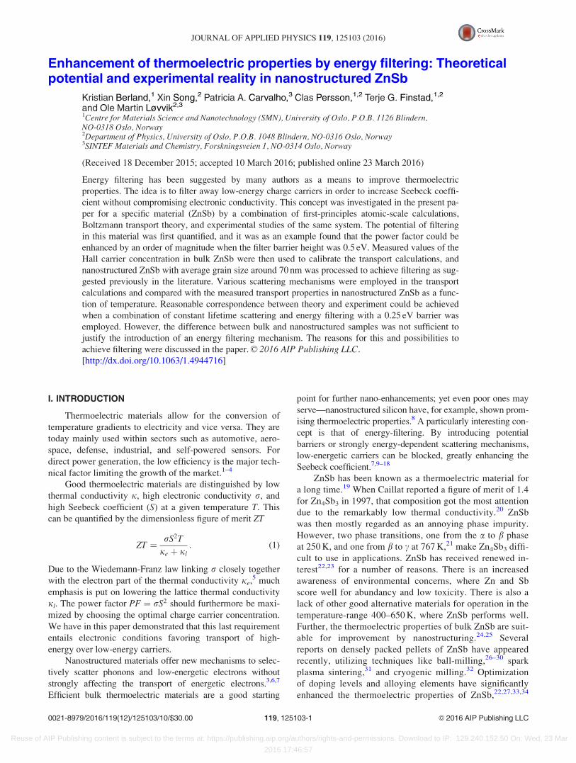
Enhancement of thermoelectric properties by energy filtering: Theoretical potential andexperimental reality in nanostructured ZnSbKristian Berland, Xin Song, Patricia A. Carvalho, Clas Persson, Terje G. Finstad, and Ole Martin Løvvik Citation: Journal of Applied Physics 119, 125103 (2016); doi: 10.1063/1.4944716 View online: http://dx.doi.org/10.1063/1.4944716 View Table of Contents: http://scitation.aip.org/content/aip/journal/jap/119/12?ver=pdfcov Published by the AIP Publishing Articles you may be interested in Hot probe measurements of n-type conduction in Sb-doped ZnO microwires J. Appl. Phys. 117, 155703 (2015); 10.1063/1.4918721 Comment on “Influence of growth mode on the structural, optical, and electrical properties of In-doped ZnOnanorods” [Appl. Phys. Lett.94, 041906 (2009)] Appl. Phys. Lett. 95, 126101 (2009); 10.1063/1.3234375 Thermoelectric properties of p -type LiZnSb: Assessment of ab initio calculations J. Appl. Phys. 105, 063701 (2009); 10.1063/1.3091267 Influence of growth mode on the structural, optical, and electrical properties of In-doped ZnO nanorods Appl. Phys. Lett. 94, 041906 (2009); 10.1063/1.3064919 Microstructure and electrical property correlations in Ga:ZnO transparent conducting thin films J. Appl. Phys. 100, 093519 (2006); 10.1063/1.2360777
Reuse of AIP Publishing content is subject to the terms at: https://publishing.aip.org/authors/rights-and-permissions. Download to IP: 129.240.152.50 On: Wed, 23 Mar
2016 17:46:57
Enhancement of thermoelectric properties by energy filtering: Theoreticalpotential and experimental reality in nanostructured ZnSb
Kristian Berland,1 Xin Song,2 Patricia A. Carvalho,3 Clas Persson,1,2 Terje G. Finstad,1,2
and Ole Martin Løvvik2,3
1Centre for Materials Science and Nanotechnology (SMN), University of Oslo, P.O.B. 1126 Blindern,NO-0318 Oslo, Norway2Department of Physics, University of Oslo, P.O.B. 1048 Blindern, NO-0316 Oslo, Norway3SINTEF Materials and Chemistry, Forskningsveien 1, NO-0314 Oslo, Norway
(Received 18 December 2015; accepted 10 March 2016; published online 23 March 2016)
Energy filtering has been suggested by many authors as a means to improve thermoelectric
properties. The idea is to filter away low-energy charge carriers in order to increase Seebeck coeffi-
cient without compromising electronic conductivity. This concept was investigated in the present pa-
per for a specific material (ZnSb) by a combination of first-principles atomic-scale calculations,
Boltzmann transport theory, and experimental studies of the same system. The potential of filtering
in this material was first quantified, and it was as an example found that the power factor could be
enhanced by an order of magnitude when the filter barrier height was 0.5 eV. Measured values of the
Hall carrier concentration in bulk ZnSb were then used to calibrate the transport calculations, and
nanostructured ZnSb with average grain size around 70 nm was processed to achieve filtering as sug-
gested previously in the literature. Various scattering mechanisms were employed in the transport
calculations and compared with the measured transport properties in nanostructured ZnSb as a func-
tion of temperature. Reasonable correspondence between theory and experiment could be achieved
when a combination of constant lifetime scattering and energy filtering with a 0.25 eV barrier was
employed. However, the difference between bulk and nanostructured samples was not sufficient to
justify the introduction of an energy filtering mechanism. The reasons for this and possibilities to
achieve filtering were discussed in the paper. VC 2016 AIP Publishing LLC.
[http://dx.doi.org/10.1063/1.4944716]
I. INTRODUCTION
Thermoelectric materials allow for the conversion of
temperature gradients to electricity and vice versa. They are
today mainly used within sectors such as automotive, aero-
space, defense, industrial, and self-powered sensors. For
direct power generation, the low efficiency is the major tech-
nical factor limiting the growth of the market.1–4
Good thermoelectric materials are distinguished by low
thermal conductivity j, high electronic conductivity r, and
high Seebeck coefficient (S) at a given temperature T. This
can be quantified by the dimensionless figure of merit ZT
ZT ¼ rS2T
je þ jl: (1)
Due to the Wiedemann-Franz law linking r closely together
with the electron part of the thermal conductivity je,5 much
emphasis is put on lowering the lattice thermal conductivity
jl. The power factor PF ¼ rS2 should furthermore be maxi-
mized by choosing the optimal charge carrier concentration.
We have in this paper demonstrated that this last requirement
entails electronic conditions favoring transport of high-
energy over low-energy carriers.
Nanostructured materials offer new mechanisms to selec-
tively scatter phonons and low-energetic electrons without
strongly affecting the transport of energetic electrons.3,6,7
Efficient bulk thermoelectric materials are a good starting
point for further nano-enhancements; yet even poor ones may
serve—nanostructured silicon have, for example, shown prom-
ising thermoelectric properties.8 A particularly interesting con-
cept is that of energy-filtering. By introducing potential
barriers or strongly energy-dependent scattering mechanisms,
low-energetic carriers can be blocked, greatly enhancing the
Seebeck coefficient.7,9–18
ZnSb has been known as a thermoelectric material for
a long time.19 When Caillat reported a figure of merit of 1.4
for Zn4Sb3 in 1997, that composition got the most attention
due to the remarkably low thermal conductivity.20 ZnSb
was then mostly regarded as an annoying phase impurity.
However, two phase transitions, one from the a to b phase
at 250 K, and one from b to c at 767 K,21 make Zn4Sb3 diffi-
cult to use in applications. ZnSb has received renewed in-
terest22,23 for a number of reasons. There is an increased
awareness of environmental concerns, where Zn and Sb
score well for abundancy and low toxicity. There is also a
lack of other good alternative materials for operation in the
temperature-range 400–650 K, where ZnSb performs well.
Further, the thermoelectric properties of bulk ZnSb are suit-
able for improvement by nanostructuring.24,25 Several
reports on densely packed pellets of ZnSb have appeared
recently, utilizing techniques like ball-milling,26–30 spark
plasma sintering,31 and cryogenic milling.32 Optimization
of doping levels and alloying elements have significantly
enhanced the thermoelectric properties of ZnSb,22,27,33,34
0021-8979/2016/119(12)/125103/10/$30.00 VC 2016 AIP Publishing LLC119, 125103-1
JOURNAL OF APPLIED PHYSICS 119, 125103 (2016)
Reuse of AIP Publishing content is subject to the terms at: https://publishing.aip.org/authors/rights-and-permissions. Download to IP: 129.240.152.50 On: Wed, 23 Mar
2016 17:46:57
utilizing the potential of the impurity band.33,35–37 This has
led to an improvement of the figure-of-merit from 0.3 in the
1960s38 to consistent reports of zT > 0:9.22,23,27
A number of theoretical studies of ZnSb have been
reported in recent years. Ab initio band structure calcula-
tions have been reported by several groups.30,33,39–45 These
have, e.g., allowed comparisons with experimental effec-
tive masses,33 the stability of the material,46 vacancy for-
mation energies revealing the nature of the bonding,44 and
charge transfer to bonds or neighbor atoms.30,47 Also, a few
phonon dispersion results and studies addressing thermal
properties of ZnSb from first principles have recently
appeared.44,48–50
In this paper, we have quantified the theoretical potential
of energy filtering in ZnSb, demonstrating that it is indeed
possible, from a theoretical point of view, to greatly enhance
the power factor of ZnSb. In an attempt to verify this experi-
mentally, we prepared nanostructured ZnSb samples by a
combination of cryomilling and rapid hot pressing, which
has been shown previously to generate densely packed pel-
lets with very small grain size and significantly reduced ther-
mal conductivity.32 Our hypothesis was that such processing
could introduce energy filtering from grain boundaries or
nanoinclusions associated with grain boundaries.13,15,17 The
transport properties of these samples were then compared to
the theoretical predictions with and without energy filtering.
This paper is organized as follows: First, a brief descrip-
tion of the sample preparation and experimental methods are
provided. Then, follows the theoretical approach to calculat-
ing the thermoelectric properties and solving the Boltzmann
transport equation with different scattering models including
energy filtering. This is followed by an analysis of the poten-
tial of energy filtering of ZnSb. A comparison between
theory and experiment for a bulk reference sample is then
presented, validating the approach qualitatively and indicat-
ing quantitative shortcomings. The final part is a comparison
between theory and experiment for nanostructured samples.
II. EXPERIMENTAL METHODS
Starting from stoichiometric Zn and Sb sealed in evac-
uated quartz tube without any intentional dopants, the initial
materials were synthesized by melting and solidification.
The mix was melted at 970 K followed by quenching in cold
water. Two thermo-mechanical processing routes were then
followed: (i) a “nanostructured” sample was produced by
ball milling at 77 K and hot-pressing at 740 K for 30 min and
cooling to RT within 2 h; (ii) a “bulk” sample, used as refer-
ence, was produced by ball milling at room temperature and
hot-pressing at 740 K for 30 min and cooling to RT within
more than 20 h. Further details on the fabrication method,
reduction of thermal conductivity in nanostructured samples,
etc., are described in Ref. 32.
A number of different methods were used to characterize
the samples: The microstructure was investigated by transmis-
sion electron microscopy and energy dispersive spectroscopy
(EDS) using an FEI Titan G2 60-300 instrument operated at
300 kV. For better statistics, the average grain size was esti-
mated from the full-width half maximum (FWHM) of X-ray
diffraction peaks using the TOPAS software, which includes
information about the instrument contributions in the peak
shape analysis.51 The Seebeck coefficient was measured with
the uniaxial four-point method in vacuum.52 Finally, the elec-
trical conductivity and the carrier concentration were meas-
ured in vacuum with the Van der Pauw and Hall methods
using a custom-built instrument.53
III. THEORY
The Boltzmann transport equation in the relaxation-time
approximation was used to calculate thermoelectric properties.
As input for these calculations, we used the electronic band
structure from density functional theory calculations together
with a specified energy filtering and constant relaxation time
s. These results were also compared with results obtained
with a simple energy (�)-dependent scattering of the form
sð�Þ ¼ ssð�=kBTÞs; (2)
where the scattering parameter s determines the energy de-
pendency and thus the specific scattering mechanism. kB is the
Boltzmann constant. Important examples include acoustic-
phonon scattering (s ¼ �0:5), polar optical phonon scattering
(s¼ 0.5), and ionized impurity scattering (s¼ 1.5).54 The net
effect of less energy-dependent scattering mechanisms, such
as scattering from neutral defects, can be represented by a con-
stant lifetime contribution (s¼ 0). The various possibilities
represented by Equation (2) can account reasonably well for
typical scattering mechanisms existing in bulk materials, at
least for scattering around nondegenerate band minima.55
Energy filtering was implemented in these calculations
by simply removing contributions to the thermoelectric
transport properties that arise from charge carriers close to
the valence band edge. According to theoretical considera-
tions, energy filtering can arise from extended barriers such
as heterostructures, nanocomposites, nanoinclusions, or grain
boundaries.9–13,15–17
A. Electronic structure calculations
The structure and electronic properties of ZnSb were cal-
culated utilizing the plane wave code VASP, working at the
density functional theory (DFT) level and using the projector
augmented wave approximation for atomic core regions.56–59
The generalized gradient Perdew-Burke-Ernzerhof (PBE)60
exchange-correlation functional was used, and spin-orbit cou-
pling was ignored.
To obtain the atomic and crystal structures, we relaxed
the structure with DFT using an energy cutoff of 500 eV,
which is 80% larger than the standard recommended maxi-
mum pseudopotential cutoff. Such high cutoffs are needed to
accurately determine the structure. The k-point sampling
was set to 10� 8� 8, and due to the low PBE band gap, the
Gaussian smearing was set to 0.03 eV. The structure was
relaxed until forces became smaller than 0.02 eV/A. The cal-
culated lattice parameters of the orthorhombic unit cell,
6.28 A, 7.82 A, and 8.22 A, agree well with previous calcula-
tions.61,62 For comparison, the experimental values at room
temperature are 6.218 A, 7.741 A, and 8.115 A.63
125103-2 Berland et al. J. Appl. Phys. 119, 125103 (2016)
Reuse of AIP Publishing content is subject to the terms at: https://publishing.aip.org/authors/rights-and-permissions. Download to IP: 129.240.152.50 On: Wed, 23 Mar
2016 17:46:57
To obtain the electronic structure, we first generated the
electronic charge density nðrÞ using an energy cutoff of
276 eV, corresponding to the recommended maximum pseu-
dopotential cutoff and a dense k-mesh of 20� 16� 16 inte-
grated using the tetrahedron method with Bl€ochl corrections.
The total energy was converged to 10�6 eV. Following
this step, we generated the band structure with a non-
selfconsistent DFT calculations with a k-mesh of 50� 50
�50, as such very dense meshes are required for accurate
transport properties.
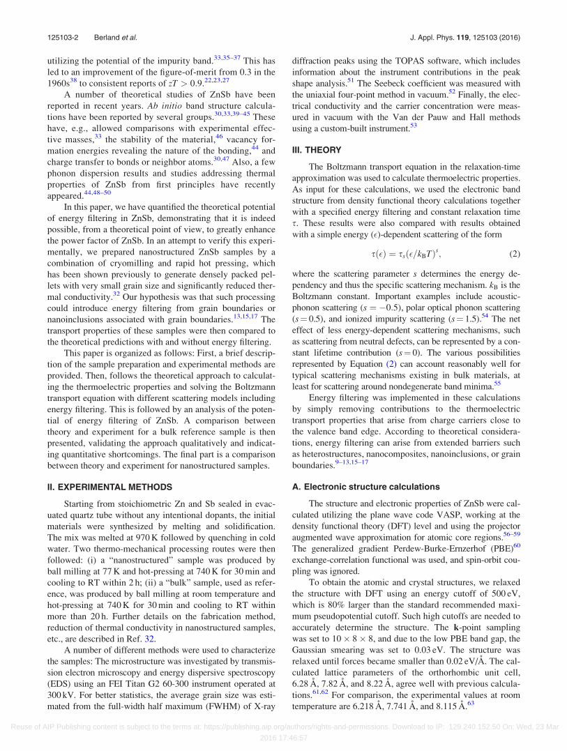
Figure 1 shows the electronic band structure of ZnSb
(left), the density of states qð�Þ (middle), and the diagonal
elements of the tensorial transport spectral functions Rð�Þ(Ref. 64) for a constant relaxation time (right). Rð�Þ is a
3� 3 tensor, and its diagonal elements are defined in the fol-
lowing manner:
Raa �ð Þ ¼1
VN
Xk;i
�ia kð Þ
� �2si kð Þ d �� �i kð Þ
� �; (3)
where V is the volume, N is the number of majority charge
carriers, siðkÞ is the relaxation time for band number i, �iðkÞis the energy of band i at reciprocal vector k, and �i
aðkÞ is the
group velocity in the a-direction (a ¼ x; y; z).
The most relevant region for low-field transport is that
close to the band edges (for energies less than, e.g., 0.5 eV
away from the Fermi level). We first note that, close to the
band edges, the level of anisotropy for Rð�Þ is somewhat
higher (the relative difference between the diagonal compo-
nents is larger) in the valence-band region than in the
conduction-band region. We have in the remainder of the pa-
per neglected the anisotropy by assuming that the samples are
multicrystalline and isotropic on average. This was imposed
by using the mean of the diagonal elements of the transport
spectral function: Rð�Þ ¼ TrðRð�ÞÞ=3. The spectral functions
are on the other hand larger in magnitude above the conduc-
tion band minimum (CBM) than below the valence band max-
imum (VBM). This can be rationalized from the shape of the
band structure (left) having a single dominant peak near the
VBM and multiple ones of relatively similar energy near the
CBM.
The presence of an impurity band originating from Zn
defects can explain many of the features of ZnSb at low
temperatures, and a model involving single parabolic bands
including an explicit impurity band was rather successful in
reproducing transport properties of intentionally undoped
ZnSb.35 In the present study, we have chosen to include con-
tributions from such impurities as an effective scattering
model combined with adapting the charge carrier concentra-
tion by changing the Fermi level. The alternative, introduc-
ing an explicit impurity band to the calculated band structure
as in Ref. 35, would imply ambiguities related to the position
and size of the impurity band. One could include the impu-
rity band indirectly by adding Zn vacancies (the most stable
intrinsic impurity in ZnSb) as in Ref. 44, but this would
make it difficult to fine-tune the doping level, particularly
without involving prohibitively large supercells. Also, our
choice gave the ability to directly compare contributions
from impurity scattering with other mechanisms.
B. Boltzmann transport equation
Key thermoelectric quantities can be expressed in terms
of integrals of the transport-spectral function Rð�Þ as
follows:
r ¼ e2
ð1�1
d� � @fFD �ð Þ@�
� �R �ð Þ ;
TrS ¼ e
ð1�1
d� � @fFD �ð Þ@�
� �R �ð Þ �� lFð Þ ;
Tj0 ¼ð1�1
d� � @fFD �ð Þ@�
� �R �ð Þ �� lFð Þ2 : (4)
Here, the derivative of the Fermi-Dirac distribution func-
tion ð� @fFDð�Þ@� Þ is the Fermi window, a symmetric function
peaked when the energy � is equal to the Fermi level, lF.
Our calculated PBE band gap of ZnSb was 0:06 eV,
which is consistent with previous studies at the same level of
theory.30,40,44 This level of theory is known to severely
underestimate the gap compared to experimental values. The
typical experimental value of the band gap for single crystal
ZnSb is 0.5–0.6 eV.19,45,65,66 However, there are also experi-
mental reports of a ZnSb band gap around 0.3 eV.67 We
chose to enlarge the calculated band gap by 0.5 eV in order
to be consistent with recent ab initio studies employing
the more reliable Heyd-Scuseria-Ernzerhof (HSE) hybrid
FIG. 1. Electronic band structure of
ZnSb obtained using the PBE
exchange-correlation functional (left),
corresponding density of states (DOS)
(middle), and diagonal elements of the
tensorial transport spectral function
(right). See text for explanation.
125103-3 Berland et al. J. Appl. Phys. 119, 125103 (2016)
Reuse of AIP Publishing content is subject to the terms at: https://publishing.aip.org/authors/rights-and-permissions. Download to IP: 129.240.152.50 On: Wed, 23 Mar
2016 17:46:57
functional, where the band gap was predicted to be
0.56 eV.30,47 The adjustment was implemented by a simple
scissor operator widening the gap in Rð�Þ and qið�Þ by
0.5 eV, keeping their shapes otherwise fixed.
Energy filtering corresponding to a nonplanar potential13
was implemented by removing the contributions from the
top of the valence band region (�¼ 0) in a width D, as
expressed in terms of Heaviside step functions h as follows:
Rð�Þ ! Rð�Þðhð��� DÞ þ hð�ÞÞ: (5)
This kind of energy filtering is crude, but rather common in
the literature.13,16
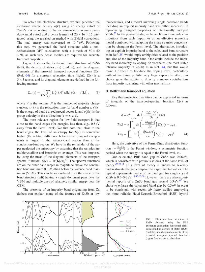
Figure 2 shows the calculated thermoelectric properties
of ZnSb as a function of the Fermi level lF. The left side
presents results at T ¼ 300 K, the right at T ¼ 500 K. Panels
show (a) the Hall carrier concentration, (b) the Seebeck coeffi-
cient, (c) the conductivity, and (d) the power factor. The full
black curves show the constant relaxation time results for
bulk ZnSb including the band gap correction specified above.
The stark contrast with the dashed one, based on the bare PBE
gap, underlines the importance of this correction. With the
low PBE gap, minority carrier contributions become signifi-
cant for low and moderate doping, severely reducing the peak
Seebeck value. Further, the asymmetry of Rð�Þ, as seen in
Figure 1, reflects a favoring of electron transport over hole
carrier transport, resulting in a negative Seebeck coefficient at
Fermi levels close to the band edges. The asymmetry is also
reflected in the shape of the conductivity and power factor,
indicating that ZnSb could be a better n-type thermoelectric
than a p-type,30,43,44 provided that stable n-type ZnSb with
suitable doping concentration could be prepared. So far no
successful n-type has been reported, while the difficulty has
been rationalized by the easy formation of Zn vacancy type
defects acting as acceptors. In this paper, emphasis has thus
been on the regular p-type variant.
The effect of various degrees of energy filtering is
shown with the thin green and dotted red curves in Figure 2.
Energy filtering drastically increases the peak Seebeck coef-
ficient and power factor, but also shifts the peak positions to
a lower Fermi level corresponding to higher p-doping con-
centrations. The particularly high peak with an energy filter-
ing parameter of D ¼ 0:5 eV can be linked to the shape of
the band structure and to the density of states and transport
spectral function in Figure 1. At energies around 0:5 eV,
additional bands start contributing causing a kink-like fea-
ture in these two functions.
Comparing the left and right subfigures, we find that for
a given Fermi level, the Seebeck coefficient is lower at
500 K than at 300 K, but as far as the power factor is con-
cerned, this is more than compensated by the increased con-
ductivity, resulting in a higher value at 500 K.
FIG. 2. Calculated (Hall) carrier concentration (a), Seebeck coefficient (b), conductivity (c), and power factor (d) of ZnSb at T ¼ 300 K (left panels) and
T ¼ 500 K (right panels) as a function of the Fermi level lF. A constant scattering time with s0 ¼ 1� 10�14 s was used. The dashed blue curves are based on
the PBE band gap (0.06 eV), while the thick black curves rely on the experimental band gap (0.56 eV). The thin green and dotted red curves are results with a
valence band energy filter of 0:25 eV and 0:5 eV.
125103-4 Berland et al. J. Appl. Phys. 119, 125103 (2016)
Reuse of AIP Publishing content is subject to the terms at: https://publishing.aip.org/authors/rights-and-permissions. Download to IP: 129.240.152.50 On: Wed, 23 Mar
2016 17:46:57
In the comparison with experimental data (in Sec. IV),
we will use the measured Hall carrier density at different
temperatures nHallðTÞ to determine the Fermi level lFðTÞ.We have then assumed that the holes and the electrons scat-
ter equally (but possibly depending on the energy of the
band). This is a minor approximation, since the transport
properties are dominated by the majority carriers for the Hall
carrier concentrations and temperatures considered here
(when assuming the band gap is 0.56 eV). In the case of con-
stant scattering time, the Fermi level could thus be obtained
for each temperature by solving the following equation:
nHallðTÞrH ¼ð1�1
d� fFDð�� lFÞqð�Þsignð�Þ þ Nval: (6)
Here, Nval is the number of valence electrons in the system,
and rH is the Hall factor. For simple energy-dependent scat-
tering (Equation (2)), we used the Hall factor55 rHðsÞ¼ Cð2sþ 5=2ÞCð5=2Þ=ðCðsþ 5=2ÞÞ2 and related the Hall
mobility to the drift mobility. Here, C is the gamma-
function. For reference, rHð0Þ ¼ 1; rHð�0:5Þ � 1:18, and
rHð1Þ ¼ 1:4. This expression ignores non-parabolicity. This
is in line with the use of simple scattering models also
derived for parabolic bands.
Care must be taken in determining the Fermi level when
energy filtering is included in the model, since filtered elec-
trons do not contribute to the Hall carrier concentration.
Thus, if a filter is used on qð�Þ in Equation (6), the reference
number of valence electrons Nval should be adjusted accord-
ingly. Further, the Hall correction factor and simple energy-
dependent relaxation time approximations become inappro-
priate as they are developed for parabolic bands. We have
therefore only combined energy-filtering models with the
constant relaxation-time approximation.
The thermoelectric transport properties were calculated
using the BoltzTraP68 software package to generate the den-
sity of states qið�Þ and the transport spectral functions Rið�Þfor each band i at constant scattering time. Next, Equations
(4) and (6) were solved in a post-processing step using
scipy69 routines in python.
C. Potential of energy filtering for ZnSb
Energy filtering greatly enhances the peak Seebeck coef-
ficient of ZnSb, as shown in Figure 2. At the same time, it
severely reduces the electrical conductivity at a given Fermi
level, since a significant number of charge carriers do not
contribute to the transport anymore. However, the Fermi
level may be manipulated if the doping level can be con-
trolled. In that case, as the Fermi level approaches the fil-
tered region, the conductivity can be considerably increased,
resulting in a strongly enhanced power factor. This is partic-
ularly so when filtering allows additional bands to contribute,
as discussed above for the case of D ¼ 0:5 eV.
Energy-dependent scattering can also enhance the
Seebeck effect. In fact, filtering can be viewed as an
extremely energy-dependent form of scattering, as, e.g., dis-
cussed by Bahk and coworkers.13 Whereas filtering may be
appropriate as a crude model of the scattering or trapping
caused by extended energy barriers such as grain bounda-
ries,7,12,70 energy-dependent expressions are better suited to
account for scattering by charged impurities such as accept-
ors or even charged nanoinclusions.13
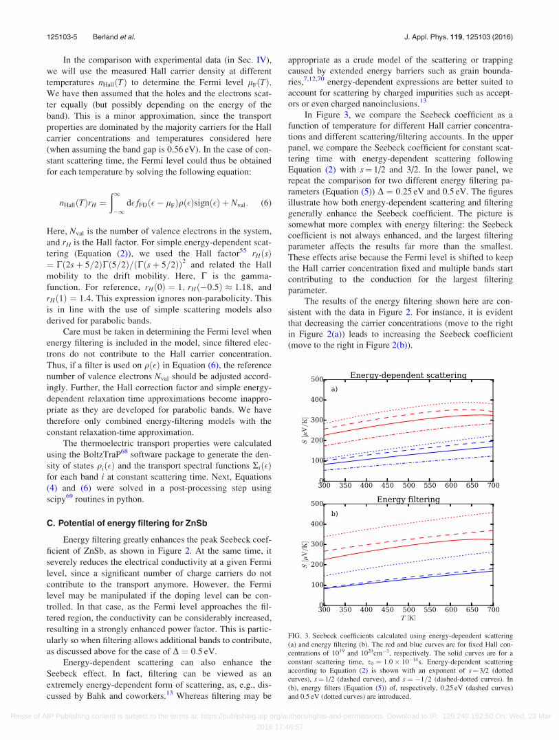
In Figure 3, we compare the Seebeck coefficient as a
function of temperature for different Hall carrier concentra-
tions and different scattering/filtering accounts. In the upper
panel, we compare the Seebeck coefficient for constant scat-
tering time with energy-dependent scattering following
Equation (2) with s¼ 1/2 and 3/2. In the lower panel, we
repeat the comparison for two different energy filtering pa-
rameters (Equation (5)) D ¼ 0:25 eV and 0.5 eV. The figures
illustrate how both energy-dependent scattering and filtering
generally enhance the Seebeck coefficient. The picture is
somewhat more complex with energy filtering: the Seebeck
coefficient is not always enhanced, and the largest filtering
parameter affects the results far more than the smallest.
These effects arise because the Fermi level is shifted to keep
the Hall carrier concentration fixed and multiple bands start
contributing to the conduction for the largest filtering
parameter.
The results of the energy filtering shown here are con-
sistent with the data in Figure 2. For instance, it is evident
that decreasing the carrier concentrations (move to the right
in Figure 2(a)) leads to increasing the Seebeck coefficient
(move to the right in Figure 2(b)).
FIG. 3. Seebeck coefficients calculated using energy-dependent scattering
(a) and energy filtering (b). The red and blue curves are for fixed Hall con-
centrations of 1019 and 1020cm�3, respectively. The solid curves are for a
constant scattering time, s0 ¼ 1:0� 10�14s. Energy-dependent scattering
according to Equation (2) is shown with an exponent of s¼ 3/2 (dotted
curves), s¼ 1/2 (dashed curves), and s ¼ �1=2 (dashed-dotted curves). In
(b), energy filters (Equation (5)) of, respectively, 0.25 eV (dashed curves)
and 0.5 eV (dotted curves) are introduced.
125103-5 Berland et al. J. Appl. Phys. 119, 125103 (2016)
Reuse of AIP Publishing content is subject to the terms at: https://publishing.aip.org/authors/rights-and-permissions. Download to IP: 129.240.152.50 On: Wed, 23 Mar
2016 17:46:57
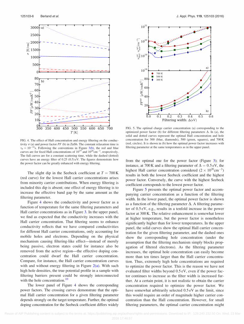
The slight dip in the Seebeck coefficient at T ¼ 700 K
(red curve) for the lowest Hall carrier concentrations arises
from minority carrier contributions. When energy filtering is
included this dip is absent; one effect of energy filtering is to
increase the effective band gap by the same amount as the
filtering parameter.
Figure 4 shows the conductivity and power factor as a
function of temperature for the same filtering parameters and
Hall carrier concentrations as in Figure 3. In the upper panel,
we find as expected that the conductivity increases with the
Hall carrier concentration. That filtering seems to enhance
conductivity reflects that we have compared conductivities
for different Hall carrier concentrations, only accounting for
mobile holes and electrons. Depending on the physical
mechanism causing filtering-like effect—instead of merely
being passive, electron states could for instance also be
removed from the active region—the effective doping con-
centration could dwarf the Hall carrier concentration.
Compare, for instance, the Hall carrier concentration curves
with and without energy filtering in Figure 2(a). With such
high hole densities, the true potential profile in a sample with
filtering barriers present could be strongly interconnected
with the hole concentration.10
The lower panel of Figure 4 shows the corresponding
power factors. The crossing curves demonstrate that the opti-
mal Hall carrier concentration for a given filtering parameter
depends strongly on the target temperature. Further, the optimal
doping concentration for the Seebeck coefficient differs widely
from the optimal one for the power factor (Figure 3); for
instance, at 700 K and a filtering parameter of D ¼ 0:5 eV, the
highest Hall carrier concentration considered (2� 1020cm�3)
results in both the lowest Seebeck coefficient and the highest
power factor. Conversely, the curve with the highest Seebeck
coefficient corresponds to the lowest power factor.
Figure 5 presents the optimal power factor and accom-
panying carrier concentration as a function of the filtering
width. In the lower panel, the optimal power factor is shown
as a function of the filtering parameter D. A filtering parame-
ter of 0.5 eV, e.g., results in a tenfold increase in the power
factor at 300 K. The relative enhancement is somewhat lower
at higher temperature, but the power factor is nonetheless
significantly higher than for lower temperatures. In the upper
panel, the solid curves show the optimal Hall carrier concen-
tration for the given filtering parameter, and the dashed ones
show the corresponding hole concentration (under the
assumption that the filtering mechanism simply blocks prop-
agation of filtered electrons). As the filtering parameter
increases, the optimal hole concentration can easily become
more than ten times larger than the Hall carrier concentra-
tion. Thus, extremely high hole concentrations are required
to optimize the power factor. This is the reason we have not
evaluated filter widths beyond 0.5 eV, even if the power fac-
tor continues to increase as the filter width is increased fur-
ther. At a certain point, it is not realistic to obtain the carrier
concentration required to optimize the power factor. We
have somewhat arbitrarily selected 0.5 eV as the limit, since
this would require an order of magnitude higher carrier con-
centration than the Hall concentration. However, for small
filtering parameters, the optimal carrier concentration might
FIG. 4. The effect of Hall concentration and energy filtering on the conduc-
tivity r (a) and power factor PF (b) in ZnSb. The constant relaxation time is
s0 ¼ 10�14s. Following the conventions in Figure 3(b), the red and blue
curves are for fixed Hall concentrations of 1019 and 1020cm�3, respectively.
The full curves are for a constant scattering time, while the dashed (dotted)
curves have an energy filter of 0.25 (0.5) eV. The figures demonstrate how
the power factor can be greatly enhanced with energy filtering.
FIG. 5. The optimal charge carrier concentration (a) corresponding to the
optimized power factor (b) for different filtering parameters D. In (a), the
solid and dotted curves represent the optimal Hall concentration and hole
concentration for 300 (blue, diamonds), 500 (green, squares), and 700 K
(red, circles). It is shown in (b) how the optimal power factor increases with
filtering parameter at the same temperatures as in the upper panel.
125103-6 Berland et al. J. Appl. Phys. 119, 125103 (2016)
Reuse of AIP Publishing content is subject to the terms at: https://publishing.aip.org/authors/rights-and-permissions. Download to IP: 129.240.152.50 On: Wed, 23 Mar
2016 17:46:57
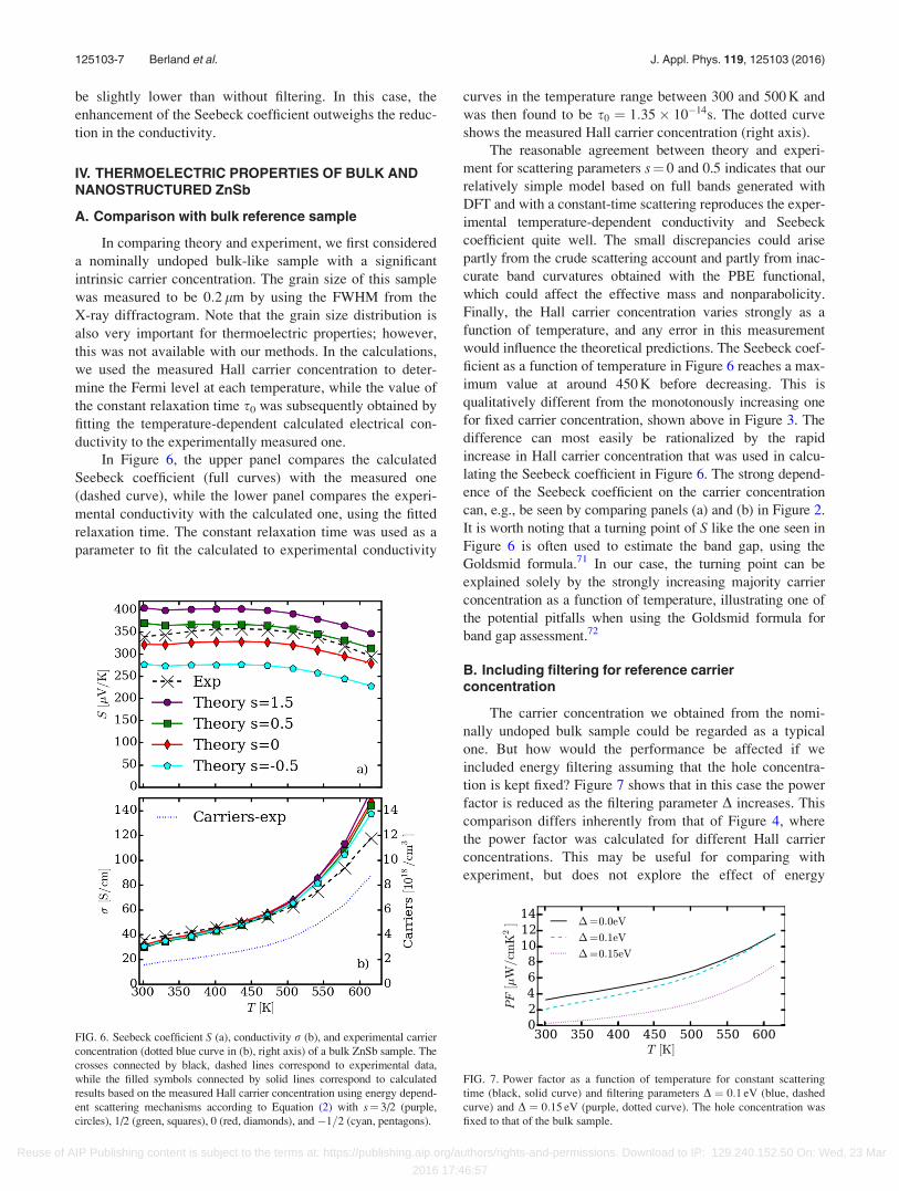
be slightly lower than without filtering. In this case, the
enhancement of the Seebeck coefficient outweighs the reduc-
tion in the conductivity.
IV. THERMOELECTRIC PROPERTIES OF BULK ANDNANOSTRUCTURED ZnSb
A. Comparison with bulk reference sample
In comparing theory and experiment, we first considered
a nominally undoped bulk-like sample with a significant
intrinsic carrier concentration. The grain size of this sample
was measured to be 0:2 lm by using the FWHM from the
X-ray diffractogram. Note that the grain size distribution is
also very important for thermoelectric properties; however,
this was not available with our methods. In the calculations,
we used the measured Hall carrier concentration to deter-
mine the Fermi level at each temperature, while the value of
the constant relaxation time s0 was subsequently obtained by
fitting the temperature-dependent calculated electrical con-
ductivity to the experimentally measured one.
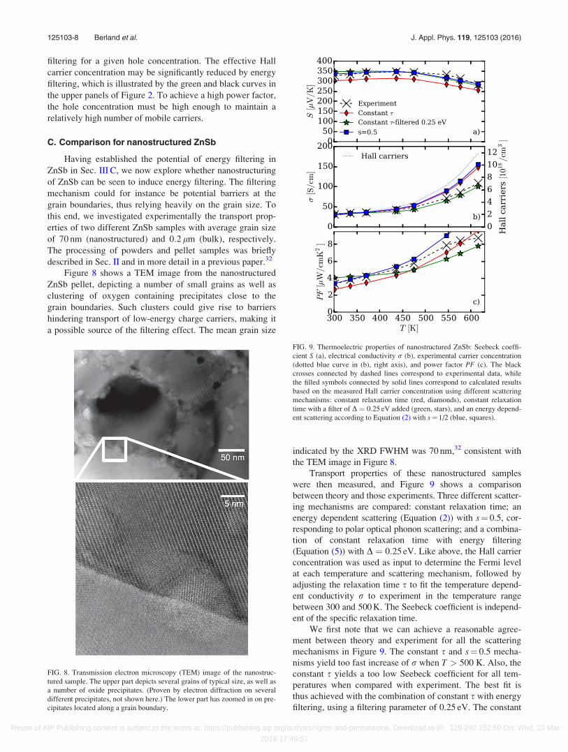
In Figure 6, the upper panel compares the calculated
Seebeck coefficient (full curves) with the measured one
(dashed curve), while the lower panel compares the experi-
mental conductivity with the calculated one, using the fitted
relaxation time. The constant relaxation time was used as a
parameter to fit the calculated to experimental conductivity
curves in the temperature range between 300 and 500 K and
was then found to be s0 ¼ 1:35� 10�14s. The dotted curve
shows the measured Hall carrier concentration (right axis).
The reasonable agreement between theory and experi-
ment for scattering parameters s¼ 0 and 0.5 indicates that our
relatively simple model based on full bands generated with
DFT and with a constant-time scattering reproduces the exper-
imental temperature-dependent conductivity and Seebeck
coefficient quite well. The small discrepancies could arise
partly from the crude scattering account and partly from inac-
curate band curvatures obtained with the PBE functional,
which could affect the effective mass and nonparabolicity.
Finally, the Hall carrier concentration varies strongly as a
function of temperature, and any error in this measurement
would influence the theoretical predictions. The Seebeck coef-
ficient as a function of temperature in Figure 6 reaches a max-
imum value at around 450 K before decreasing. This is
qualitatively different from the monotonously increasing one
for fixed carrier concentration, shown above in Figure 3. The
difference can most easily be rationalized by the rapid
increase in Hall carrier concentration that was used in calcu-
lating the Seebeck coefficient in Figure 6. The strong depend-
ence of the Seebeck coefficient on the carrier concentration
can, e.g., be seen by comparing panels (a) and (b) in Figure 2.
It is worth noting that a turning point of S like the one seen in
Figure 6 is often used to estimate the band gap, using the
Goldsmid formula.71 In our case, the turning point can be
explained solely by the strongly increasing majority carrier
concentration as a function of temperature, illustrating one of
the potential pitfalls when using the Goldsmid formula for
band gap assessment.72
B. Including filtering for reference carrierconcentration
The carrier concentration we obtained from the nomi-
nally undoped bulk sample could be regarded as a typical
one. But how would the performance be affected if we
included energy filtering assuming that the hole concentra-
tion is kept fixed? Figure 7 shows that in this case the power
factor is reduced as the filtering parameter D increases. This
comparison differs inherently from that of Figure 4, where
the power factor was calculated for different Hall carrier
concentrations. This may be useful for comparing with
experiment, but does not explore the effect of energy
FIG. 6. Seebeck coefficient S (a), conductivity r (b), and experimental carrier
concentration (dotted blue curve in (b), right axis) of a bulk ZnSb sample. The
crosses connected by black, dashed lines correspond to experimental data,
while the filled symbols connected by solid lines correspond to calculated
results based on the measured Hall carrier concentration using energy depend-
ent scattering mechanisms according to Equation (2) with s¼ 3/2 (purple,
circles), 1/2 (green, squares), 0 (red, diamonds), and �1=2 (cyan, pentagons).
FIG. 7. Power factor as a function of temperature for constant scattering
time (black, solid curve) and filtering parameters D ¼ 0:1 eV (blue, dashed
curve) and D ¼ 0:15 eV (purple, dotted curve). The hole concentration was
fixed to that of the bulk sample.
125103-7 Berland et al. J. Appl. Phys. 119, 125103 (2016)
Reuse of AIP Publishing content is subject to the terms at: https://publishing.aip.org/authors/rights-and-permissions. Download to IP: 129.240.152.50 On: Wed, 23 Mar
2016 17:46:57
filtering for a given hole concentration. The effective Hall
carrier concentration may be significantly reduced by energy
filtering, which is illustrated by the green and black curves in
the upper panels of Figure 2. To achieve a high power factor,
the hole concentration must be high enough to maintain a
relatively high number of mobile carriers.
C. Comparison for nanostructured ZnSb
Having established the potential of energy filtering in
ZnSb in Sec. III C, we now explore whether nanostructuring
of ZnSb can be seen to induce energy filtering. The filtering
mechanism could for instance be potential barriers at the
grain boundaries, thus relying heavily on the grain size. To
this end, we investigated experimentally the transport prop-
erties of two different ZnSb samples with average grain size
of 70 nm (nanostructured) and 0:2 lm (bulk), respectively.
The processing of powders and pellet samples was briefly
described in Sec. II and in more detail in a previous paper.32
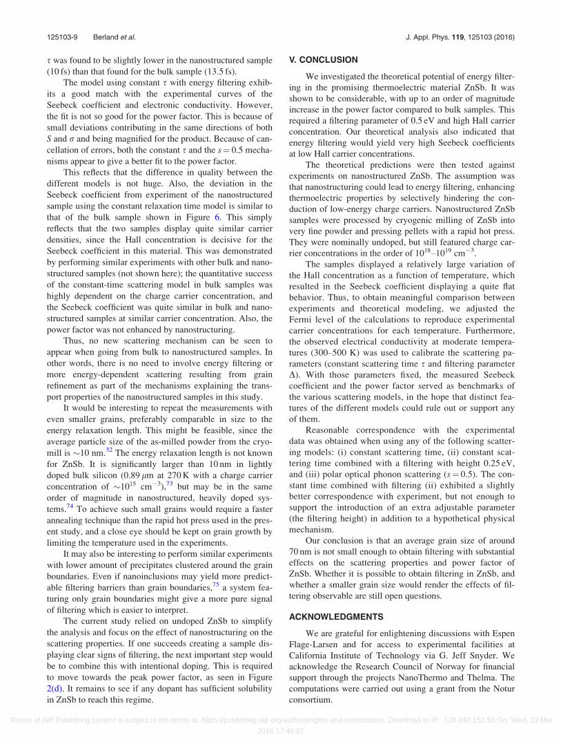
Figure 8 shows a TEM image from the nanostructured
ZnSb pellet, depicting a number of small grains as well as
clustering of oxygen containing precipitates close to the
grain boundaries. Such clusters could give rise to barriers
hindering transport of low-energy charge carriers, making it
a possible source of the filtering effect. The mean grain size
indicated by the XRD FWHM was 70 nm,32 consistent with
the TEM image in Figure 8.
Transport properties of these nanostructured samples
were then measured, and Figure 9 shows a comparison
between theory and those experiments. Three different scatter-
ing mechanisms are compared: constant relaxation time; an
energy dependent scattering (Equation (2)) with s¼ 0.5, cor-
responding to polar optical phonon scattering; and a combina-
tion of constant relaxation time with energy filtering
(Equation (5)) with D ¼ 0:25 eV. Like above, the Hall carrier
concentration was used as input to determine the Fermi level
at each temperature and scattering mechanism, followed by
adjusting the relaxation time s to fit the temperature depend-
ent conductivity r to experiment in the temperature range
between 300 and 500 K. The Seebeck coefficient is independ-
ent of the specific relaxation time.
We first note that we can achieve a reasonable agree-
ment between theory and experiment for all the scattering
mechanisms in Figure 9. The constant s and s¼ 0.5 mecha-
nisms yield too fast increase of r when T > 500 K. Also, the
constant s yields a too low Seebeck coefficient for all tem-
peratures when compared with experiment. The best fit is
thus achieved with the combination of constant s with energy
filtering, using a filtering parameter of 0.25 eV. The constant
FIG. 8. Transmission electron microscopy (TEM) image of the nanostruc-
tured sample. The upper part depicts several grains of typical size, as well as
a number of oxide precipitates. (Proven by electron diffraction on several
different precipitates, not shown here.) The lower part has zoomed in on pre-
cipitates located along a grain boundary.
FIG. 9. Thermoelectric properties of nanostructured ZnSb: Seebeck coeffi-
cient S (a), electrical conductivity r (b), experimental carrier concentration
(dotted blue curve in (b), right axis), and power factor PF (c). The black
crosses connected by dashed lines correspond to experimental data, while
the filled symbols connected by solid lines correspond to calculated results
based on the measured Hall carrier concentration using different scattering
mechanisms: constant relaxation time (red, diamonds), constant relaxation
time with a filter of D ¼ 0:25 eV added (green, stars), and an energy depend-
ent scattering according to Equation (2) with s¼ 1/2 (blue, squares).
125103-8 Berland et al. J. Appl. Phys. 119, 125103 (2016)
Reuse of AIP Publishing content is subject to the terms at: https://publishing.aip.org/authors/rights-and-permissions. Download to IP: 129.240.152.50 On: Wed, 23 Mar
2016 17:46:57
s was found to be slightly lower in the nanostructured sample
(10 fs) than that found for the bulk sample (13:5 fs).
The model using constant s with energy filtering exhib-
its a good match with the experimental curves of the
Seebeck coefficient and electronic conductivity. However,
the fit is not so good for the power factor. This is because of
small deviations contributing in the same directions of both
S and r and being magnified for the product. Because of can-
cellation of errors, both the constant s and the s¼ 0.5 mecha-
nisms appear to give a better fit to the power factor.
This reflects that the difference in quality between the
different models is not huge. Also, the deviation in the
Seebeck coefficient from experiment of the nanostructured
sample using the constant relaxation time model is similar to
that of the bulk sample shown in Figure 6. This simply
reflects that the two samples display quite similar carrier
densities, since the Hall concentration is decisive for the
Seebeck coefficient in this material. This was demonstrated
by performing similar experiments with other bulk and nano-
structured samples (not shown here); the quantitative success
of the constant-time scattering model in bulk samples was
highly dependent on the charge carrier concentration, and
the Seebeck coefficient was quite similar in bulk and nano-
structured samples at similar carrier concentration. Also, the
power factor was not enhanced by nanostructuring.
Thus, no new scattering mechanism can be seen to
appear when going from bulk to nanostructured samples. In
other words, there is no need to involve energy filtering or
more energy-dependent scattering resulting from grain
refinement as part of the mechanisms explaining the trans-
port properties of the nanostructured samples in this study.
It would be interesting to repeat the measurements with
even smaller grains, preferably comparable in size to the
energy relaxation length. This might be feasible, since the
average particle size of the as-milled powder from the cryo-
mill is �10 nm.32 The energy relaxation length is not known
for ZnSb. It is significantly larger than 10 nm in lightly
doped bulk silicon (0.89 lm at 270 K with a charge carrier
concentration of �1015 cm�3),73 but may be in the same
order of magnitude in nanostructured, heavily doped sys-
tems.74 To achieve such small grains would require a faster
annealing technique than the rapid hot press used in the pres-
ent study, and a close eye should be kept on grain growth by
limiting the temperature used in the experiments.
It may also be interesting to perform similar experiments
with lower amount of precipitates clustered around the grain
boundaries. Even if nanoinclusions may yield more predict-
able filtering barriers than grain boundaries,75 a system fea-
turing only grain boundaries might give a more pure signal
of filtering which is easier to interpret.
The current study relied on undoped ZnSb to simplify
the analysis and focus on the effect of nanostructuring on the
scattering properties. If one succeeds creating a sample dis-
playing clear signs of filtering, the next important step would
be to combine this with intentional doping. This is required
to move towards the peak power factor, as seen in Figure
2(d). It remains to see if any dopant has sufficient solubility
in ZnSb to reach this regime.
V. CONCLUSION
We investigated the theoretical potential of energy filter-
ing in the promising thermoelectric material ZnSb. It was
shown to be considerable, with up to an order of magnitude
increase in the power factor compared to bulk samples. This
required a filtering parameter of 0.5 eV and high Hall carrier
concentration. Our theoretical analysis also indicated that
energy filtering would yield very high Seebeck coefficients
at low Hall carrier concentrations.
The theoretical predictions were then tested against
experiments on nanostructured ZnSb. The assumption was
that nanostructuring could lead to energy filtering, enhancing
thermoelectric properties by selectively hindering the con-
duction of low-energy charge carriers. Nanostructured ZnSb
samples were processed by cryogenic milling of ZnSb into
very fine powder and pressing pellets with a rapid hot press.
They were nominally undoped, but still featured charge car-
rier concentrations in the order of 1018–1019 cm�3.
The samples displayed a relatively large variation of
the Hall concentration as a function of temperature, which
resulted in the Seebeck coefficient displaying a quite flat
behavior. Thus, to obtain meaningful comparison between
experiments and theoretical modeling, we adjusted the
Fermi level of the calculations to reproduce experimental
carrier concentrations for each temperature. Furthermore,
the observed electrical conductivity at moderate tempera-
tures (300–500 K) was used to calibrate the scattering pa-
rameters (constant scattering time s and filtering parameter
D). With those parameters fixed, the measured Seebeck
coefficient and the power factor served as benchmarks of
the various scattering models, in the hope that distinct fea-
tures of the different models could rule out or support any
of them.
Reasonable correspondence with the experimental
data was obtained when using any of the following scatter-
ing models: (i) constant scattering time, (ii) constant scat-
tering time combined with a filtering with height 0.25 eV,
and (iii) polar optical phonon scattering (s¼ 0.5). The con-
stant time combined with filtering (ii) exhibited a slightly
better correspondence with experiment, but not enough to
support the introduction of an extra adjustable parameter
(the filtering height) in addition to a hypothetical physical
mechanism.
Our conclusion is that an average grain size of around
70 nm is not small enough to obtain filtering with substantial
effects on the scattering properties and power factor of
ZnSb. Whether it is possible to obtain filtering in ZnSb, and
whether a smaller grain size would render the effects of fil-
tering observable are still open questions.
ACKNOWLEDGMENTS
We are grateful for enlightening discussions with Espen
Flage-Larsen and for access to experimental facilities at
California Institute of Technology via G. Jeff Snyder. We
acknowledge the Research Council of Norway for financial
support through the projects NanoThermo and Thelma. The
computations were carried out using a grant from the Notur
consortium.
125103-9 Berland et al. J. Appl. Phys. 119, 125103 (2016)
Reuse of AIP Publishing content is subject to the terms at: https://publishing.aip.org/authors/rights-and-permissions. Download to IP: 129.240.152.50 On: Wed, 23 Mar
2016 17:46:57
1M. Telkes, J. Appl. Phys. 18, 1116 (1947).2G. J. Snyder, in The Electrochemical Society Interface (Fall 2008) (2008),
p. 54.3M. Zebarjadi, K. Esfarjani, M. S. Dresselhaus, Z. F. Ren, and G. Chen,
Energy Environ. Sci. 5, 5147 (2012).4H. B. Radousky and H. Liang, Nanotechnology 23, 502001 (2012).5R. P. Chasmar and R. Stratton, J. Electron. Control 7, 52 (1959).6S. V. Faleev and F. L�eonard, Phys. Rev. B 77, 214304 (2008).7D. Narducci, S. Frabboni, and X. Zianni, J. Mater. Chem. C 3, 12176
(2015).8S. K. Bux, R. G. Blair, P. K. Gogna, H. Lee, G. Chen, M. S. Dresselhaus,
R. B. Kaner, and J.-P. Fleurial, Adv. Funct. Mater. 19, 2445 (2009).9G. Zeng, J. M. O. Zide, W. Kim, J. E. Bowers, A. C. Gossard, Z. Bian, Y.
Zhang, A. Shakouri, S. L. Singer, and A. Majumdar, J. Appl. Phys. 101,
034502 (2007).10M. Bachmann, M. Czerner, and C. Heiliger, Phys. Rev. B 86, 115320
(2012).11A. M. Dehkordi, M. Zebarjadi, J. He, and T. M. Tritt, Mater. Sci. Eng., R
97, 1 (2015).12J. Martin, L. Wang, L. Chen, and G. S. Nolas, Phys. Rev. B 79, 115311
(2009).13J.-H. Bahk, Z. Bian, and A. Shakouri, Phys. Rev. B 87, 075204 (2013).14X. H. Yang, X. Y. Qin, J. Zhang, D. Li, H. X. Xin, and M. Liu, J. Alloys
Compd. 558, 203 (2013).15D. Narducci, E. Selezneva, G. Cerofolini, S. Frabboni, and G. Ottaviani,
J. Solid State Chem. 193, 19 (2012).16E. Flage-Larsen and O. M. Løvvik, “Band structure guidelines for higher
figure-of-merit; analytic band generation and energy filtering,”
Thermoelectrics and Its Energy Harvesting (CRC Press Inc., 2012), Chap. 10.17A. Popescu, L. M. Woods, J. Martin, and G. S. Nolas, Phys. Rev. B 79,
205302 (2009).18T. Zou, X. Qin, D. Li, B. Ren, G. Sun, Y. Dou, Y. Li, L. Li, J. Zhang, and
H. Xin, J. Appl. Phys. 115, 053710 (2014).19P. J. Shaver and J. Blair, Phys. Rev. 141, 649 (1966).20G. J. Snyder, M. Christensen, E. Nishibori, T. Caillat, and B. B. Iversen,
Nat. Mater. 3, 458 (2004).21V. Izard, M. C. Record, J. C. Tedenac, and S. G. Fries, Calphad 25, 567
(2001).22D.-B. Xiong, N. L. Okamoto, and H. Inui, Scr. Mater. 69, 397 (2013).23M. Fedorov, L. Prokofeva, D. Pshenay-Severin, A. Shabaldin, and P.
Konstantinov, J. Electron. Mater. 43, 2314 (2014).24C. J. Vineis, A. Shakouri, A. Majumdar, and M. G. Kanatzidis, Adv.
Mater. 22, 3970 (2010).25M. Dresselhaus, G. Chen, M. Tang, R. Yang, H. Lee, D. Wang, Z. Ren, J.-
P. Fleurial, and P. Gogna, Adv. Mater. 19, 1043 (2007).26P. H. M. B€ottger, G. S. Pomrehn, G. J. Snyder, and T. G. Finstad, Phys.
Status Solidi A 208, 2753 (2011).27K. Valset, P. H. M. B€ottger, J. Taftø, and T. G. Finstad, J. Appl. Phys. 111,
023703 (2012).28P. M. B€ottger, K. Valset, S. Deledda, and T. G. Finstad, J. Electron. Mater.
39, 1583 (2010).29C. Okamura, T. Ueda, and K. Hasezaki, Mater. Trans. 51, 860 (2010).30K. Niedziolka, R. Pothin, F. Rouessac, R. M. Ayral, and P. Jund, J. Phys.:
Condens. Matter 26, 365401 (2014).31A. B. Blichfeld and B. B. Iversen, J. Mater. Chem. C 3, 10543 (2015).32X. Song, K. Valset, J. Graff, A. Thøgersen, A. Gunnæs, S. Luxsacumar, O.
M. Løvvik, G. Snyder, and T. Finstad, J. Electron. Mater. 44, 2578 (2015).33P. H. M. B€ottger, S. Diplas, E. Flage-Larsen, O. Prytz, and T. G. Finstad,
J. Phys.: Condens. Matter 23, 265502 (2011).34M. Fedorov, L. Prokofieva, Y. Ravich, P. Konstantinov, D. Pshenay-
Severin, and A. Shabaldin, Semiconductors 48, 432 (2014).35X. Song, P. H. M. B€ottger, O. B. Karlsen, T. G. Finstad, and J. Taftø,
Phys. Scr. T148, 014001 (2012).36K. Valset, X. Song, and T. G. Finstad, J. Appl. Phys. 117, 045709 (2015).37D. Ekl€of, A. Fischer, Y. Wu, E.-W. Scheidt, W. Scherer, and U.
Haussermann, J. Mater. Chem. A 1, 1407 (2013).38E. Justi, W. Rasch, and G. Schneider, Adv. Energy Convers. 4, 27 (1964).
39A. S. Mikhaylushkin, J. Nylen, and U. H€aussermann, Chem.: Eur. J. 11,
4912 (2005).40D. Benson, O. F. Sankey, and U. H€aussermann, Phys. Rev. B 84, 125211
(2011).41J. H. Zhao, E. J. Han, T. M. Liu, and W. Zeng, Int. J. Mol. Sci. 12, 3162
(2011).42L. Bjerg, G. K. H. Madsen, and B. B. Iversen, Chem. Mater. 23, 3907
(2011).43L. Bjerg, G. K. H. Madsen, and B. B. Iversen, Chem. Mater. 24, 2111
(2012).44P. Jund, R. Viennois, X. Tao, K. Niedziolka, and J.-C. T�edenac, Phys.
Rev. B 85, 224105 (2012).45U. H€aussermann and A. S. Mikhaylushkin, Dalton Trans. 39, 1036 (2010).46S. B. Y. Mozharivskyj, A. O. Pecharsky, and G. J. Miller, Chem. Mater.
16, 1580 (2004).47K. Niedziolka and P. Jund, J. Electron. Mater. 44, 1540 (2015).48L. Bjerg, B. B. Iversen, and G. K. H. Madsen, Phys. Rev. B 89, 024304
(2014).49A. Fischer, E.-W. Scheidt, W. Scherer, D. E. Benson, Y. Wu, D. Ekl€of,
and U. H€aussermann, Phys. Rev. B 91, 224309 (2015).50P. Hermet, M. M. Koza, C. Ritter, C. Reibel, and R. Viennois, RSC Adv.
5, 87118 (2015).51See http://www.topas-academic.net/ for “TOPAS-academic v5,” accessed:
2016-01-28.52S. Iwanaga, E. S. Toberer, A. LaLonde, and G. J. Snyder, Rev. Sci.
Instrum. 82, 063905 (2011).53K. A. Borup, E. S. Toberer, L. D. Zoltan, G. Nakatsukasa, M. Errico, J.-P.
Fleurial, B. B. Iversen, and G. J. Snyder, Rev. Sci. Instrum. 83, 123902
(2012).54P. Pichanusakorn and P. Bandaru, Mater. Sci. Eng., R 67, 19 (2010).55M. Lundstrom, Fundamentals of Carrier Transport (Cambridge
University Press, 2009).56G. Kresse and J. Hafner, Phys. Rev. B 47, 558 (1993).57G. Kresse and J. Hafner, Phys. Rev. B 49, 14251 (1994).58G. Kresse and J. Furthm€uller, Comput. Mater. Sci. 6, 15 (1996).59G. Kresse and J. Furthm€uller, Phys. Rev. B 54, 11169 (1996).60J. P. Perdew, K. Burke, and M. Ernzerhof, Phys. Rev. Lett. 77, 3865
(1996).61A. Jain, S. P. Ong, G. Hautier, W. Chen, W. D. Richards, S. Dacek, S.
Cholia, D. Gunter, D. Skinner, G. Ceder, and K. A. Persson, APL Mater.
1, 011002 (2013).62M. de Jong, W. Chen, T. Angsten, A. Jain, R. Notestine, A. Gamst, M.
Sluiter, C. Krishna Ande, S. van der Zwaag, J. J. Plata, C. Toher, S.
Curtarolo, G. Ceder, K. A. Persson, and M. Asta, Sci. Data 2, 150009
(2015).63K. E. Almin, Acta Chem. Scand. 2, 400 (1948).64G. D. Mahan and J. O. Sofo, Proc. Natl. Acad. Sci. 93, 7436 (1996).65W. J. Turner, A. S. Fischler, and W. E. Reese, Phys. Rev. 121, 759 (1961).66Non-Tetrahedrally Bonded Elements and Binary Compounds I, Landolt-
B€ornstein - Group III Condensed Matter Vol. 41C, edited by O. Madelung,
U. R€ossler, and M. Schulz (Springer Berlin Heidelberg, 1998), pp. 1–4.67L. T. Zhang, M. Tsutsui, K. Ito, and M. Yamaguchi, J. Alloys Compd.
358, 252 (2003).68G. K. H. Madsen and D. J. Singh, Comput. Phys. Commun. 175, 67
(2006).69E. Jones, T. Oliphant, and P. Peterson et al., “SciPy: Open source scientific
tools for Python,” (2001).70N. Neophytou, X. Zianni, H. Kosina, S. Frabboni, B. Lorenzi, and D.
Narducci, Nanotechnology 24, 205402 (2013).71H. J. Goldsmid and J. W. Sharp, J. Electron. Mater. 28, 869–872 (1999).72Z. M. Gibb, H.-S. Kim, H. Wang, and G. J. Snyder, Appl. Phys. Lett. 106,
022112 (2015).73N. A. Porter and C. H. Marrows, J. Appl. Phys. 111, 043719 (2012).74R. Kim and M. S. Lundstrom, J. Appl. Phys. 111, 024508 (2012).75Y. Zhang, J. H. Bahk, J. Lee, C. S. Birkel, M. L. Snedaker, D. Liu, H.
Zeng, M. Moskovits, A. Shakouri, and G. D. Stucky, Adv. Mater. 26, 2755
(2014).
125103-10 Berland et al. J. Appl. Phys. 119, 125103 (2016)
Reuse of AIP Publishing content is subject to the terms at: https://publishing.aip.org/authors/rights-and-permissions. Download to IP: 129.240.152.50 On: Wed, 23 Mar
2016 17:46:57