Embed Size (px)
Citation preview
Real-World Component Characteristics 10.1
hen is an inductor not an inductor? When it’s a capacitor! This statement may seem odd, but itsuggests the main message of this chapter. In the earlier chapters about DC and AC Theory,the basic components of electronic circuits were introduced. You saw that each has its own
unique function to perform. For example, a capacitor stores energy in an electric field, a diode rectifiescurrent and a battery provides voltage. All of these unique and different functions are necessary in orderto build large circuits that perform useful tasks. The first part of this chapter, up to Low-FrequencyTransistor Models, was written by Leonard Kay, K1NU.
As you may know from experience, these component pictures are ideal. That is, they are perfectmathematical pictures. An ideal component (or element) by definition behaves exactly like the math-ematical equations that describe it, and only in that fashion. For example, an ideal capacitor passes acurrent that is equal to the capacitance C times the rate of change of the voltage across it. Period, endof sentence.
We call any other exhibited behavior either nonideal, nonlinear or parasitic. Nonideal behavior is ageneral term that covers any deviation from the theoretical picture. Ideal circuit elements are oftenlinear: The graphs of their current versus voltage characteristics are straight lines when plotted on asuitable (Cartesian, rectangular) set of axes. We therefore call deviation from this behavior nonlinear:For example, as current through a resistor exceeds its power rating, the resistor heats up and its resistancechanges. As a result, a graph of current versus voltage is no longer a straight line.
When a component begins to exhibit properties of a different component, as when a capacitor allowsa dc current to pass through it, we call this behavior parasitic. Nonlinear and parasitic behavior are bothexamples of nonideal behavior.
Much to the bane of experimenters and design engineers, ideal components exist only in electronicstextbooks and computer programs. Real components, the ones we use, only approximate ideal compo-nents (albeit very closely in most cases).
Real diodes store minuscule energy in electric fields (junction capacitance) and magnetic fields (leadinductance); real capacitors conduct some dc (modeled by a parallel resistance), and real battery voltageis not perfectly constant (it may even decrease nonlinearly during discharge).
Knowing to what extent and under what conditions real components cease to behave like their idealcounterparts, and what can be done to account for these behaviors, is the subject of component or circuitmodeling. In this chapter, we will explore how and why the real components behave differently fromideal components, how we can account for those differences when analyzing circuits, how to select
10
Real-WorldComponent Characteristics
W
10.2 Chapter 10
components to minimize, or exploit, nonideal behaviors and give a brief introduction to computer-aidedcircuit modeling.
Much of this chapter may seem intuitive. For example, you probably know that #20 hookup wire worksjust fine for wiring many experimental circuits. When testing a circuit after construction, you probablydon’t even think about the voltage drops across those pieces of wire (you inherently assume that theyhave zero resistance). But, connect that same #20 wire directly across a car battery—with no other seriesresistance—and suddenly, the resistance of the wire does matter, and it changes—as the wire heats, meltsand breaks—from a very small value to infinity!
Real-World Component Characteristics 10.3
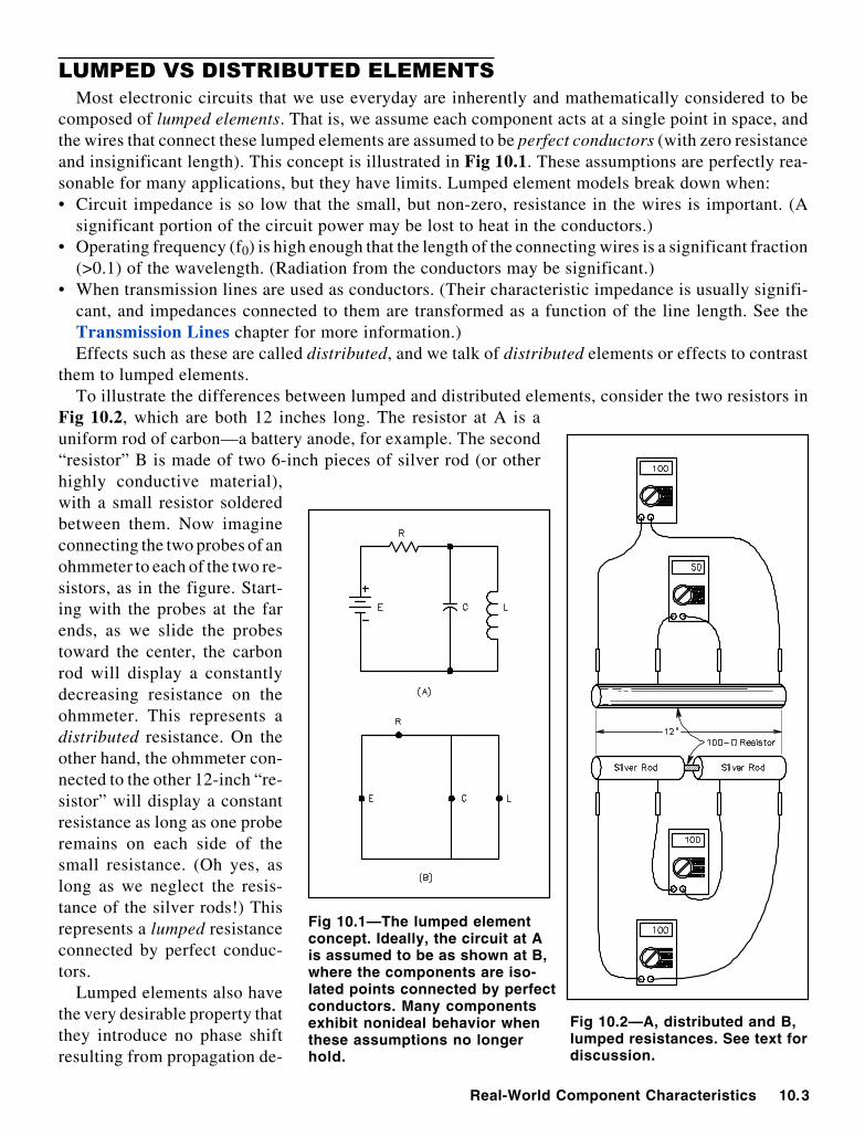
Fig 10.1—The lumped elementconcept. Ideally, the circuit at Ais assumed to be as shown at B,where the components are iso-lated points connected by perfectconductors. Many componentsexhibit nonideal behavior whenthese assumptions no longerhold.
Fig 10.2—A, distributed and B,lumped resistances. See text fordiscussion.
Most electronic circuits that we use everyday are inherently and mathematically considered to becomposed of lumped elements. That is, we assume each component acts at a single point in space, andthe wires that connect these lumped elements are assumed to be perfect conductors (with zero resistanceand insignificant length). This concept is illustrated in Fig 10.1. These assumptions are perfectly rea-sonable for many applications, but they have limits. Lumped element models break down when:• Circuit impedance is so low that the small, but non-zero, resistance in the wires is important. (A
significant portion of the circuit power may be lost to heat in the conductors.)• Operating frequency (f0) is high enough that the length of the connecting wires is a significant fraction
(>0.1) of the wavelength. (Radiation from the conductors may be significant.)• When transmission lines are used as conductors. (Their characteristic impedance is usually signifi-
cant, and impedances connected to them are transformed as a function of the line length. See theTransmission Lines chapter for more information.)Effects such as these are called distributed, and we talk of distributed elements or effects to contrast
them to lumped elements.To illustrate the differences between lumped and distributed elements, consider the two resistors in
Fig 10.2, which are both 12 inches long. The resistor at A is auniform rod of carbon—a battery anode, for example. The second“resistor” B is made of two 6-inch pieces of silver rod (or otherhighly conductive material),with a small resistor solderedbetween them. Now imagineconnecting the two probes of anohmmeter to each of the two re-sistors, as in the figure. Start-ing with the probes at the farends, as we slide the probestoward the center, the carbonrod will display a constantlydecreasing resistance on theohmmeter. This represents adistributed resistance. On theother hand, the ohmmeter con-nected to the other 12-inch “re-sistor” will display a constantresistance as long as one proberemains on each side of thesmall resistance. (Oh yes, aslong as we neglect the resis-tance of the silver rods!) Thisrepresents a lumped resistanceconnected by perfect conduc-tors.
Lumped elements also havethe very desirable property thatthey introduce no phase shiftresulting from propagation de-
10.4 Chapter 10
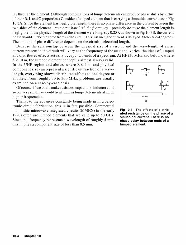
lay through the element. (Although combinations of lumped elements can produce phase shifts by virtueof their R, L and C properties.) Consider a lumped element that is carrying a sinusoidal current, as in Fig10.3A. Since the element has negligible length, there is no phase difference in the current between thetwo sides of the element—no matter how high the frequency—precisely because the element length isnegligible. If the physical length of the element were long, say 0.25 λ as shown in Fig 10.3B, the currentphase would not be the same from end to end. In this instance, the current is delayed 90 electrical degrees.The amount of phase difference depends on the circuit’s electrical length.
Because the relationship between the physical size of a circuit and the wavelength of an accurrent present in the circuit will vary as the frequency of the ac signal varies, the ideas of lumpedand distributed effects actually occupy two ends of a spectrum. At HF (30 MHz and below), whereλ ≥ 10 m, the lumped element concept is almost always valid.In the UHF region and above, where λ ≤ 1 m and physicalcomponent size can represent a significant fraction of a wave-length, everything shows distributed effects to one degree oranother. From roughly 30 to 300 MHz, problems are usuallyexamined on a case-by-case basis.
Of course, if we could make resistors, capacitors, inductors andso on, very small, we could treat them as lumped elements at muchhigher frequencies.
Thanks to the advances constantly being made in microelec-tronic circuit fabrication, this is in fact possible. Commercialmonolithic microwave integrated circuits (MMICs) in the early1990s often use lumped elements that are valid up to 50 GHz.Since this frequency represents a wavelength of roughly 5 mm,this implies a component size of less than 0.5 mm.
Fig 10.3—The effects of distrib-uted resistance on the phase of asinusoidal current. There is nophase delay between ends of alumped element.
Real-World Component Characteristics 10.5
Every circuit element behaves nonideally in some respect and under some conditions. It helps toknow the most common types of nonideal behavior so we can design and build circuits that willperform as intended under expected ranges of operating conditions. In the sections below, we willdiscuss the basic components in order of increasing common nonideal behavior. Please note thatmuch of this section applies only through HF; the peculiarities of VHF frequencies and above arediscussed later in the chapter.
First, remember that some of the common limitations associated with real components are manufac-turing concerns: tolerance and standard values. Tolerance is the measure of how much the actual valueof a component may differ from its labeled value; it is usually expressed in percent. By convention, a“higher” (actually closer) tolerance component indicates a lower (lesser) percentage deviation and willusually cost more. For example, a 1-kΩ resistor with a 5% tolerance has an actual resistance of anywherefrom 950 to 1050 Ω. When designing circuits be careful to include the effects of tolerance. More specificexamples will be discussed below.
Keep standard values in mind because not every conceivable component value is available. Forinstance, if circuit calculations yield a 4,932-Ω resistor for a demanding application, there may betrouble. The nearest commonly available values are 4700 Ω and 5600 Ω, and they’ll be rated at 5%tolerance!
These two constraints prevent us from building circuits that do precisely what we wish. In fact, themeasured performance of any circuit is the summation of the tolerances and temperature characteristicsof all the components in both the circuit under test and the test equipment itself. As a result, most circuitsare designed to operate within tolerances such as “up to a certain power” or “within this frequencyrange.” Some circuits have one or more adjustable components that can compensate for variations inothers. These limitations are then further complicated by other problems.
RESISTORS
Resistors are made in several different ways: carbon composition, carbon film, metal film, and wirewound. Carbon composition resistors are simply small cylinders of carbon mixed with various bindingagents. Carbon is technically a semiconductor and can be doped with various impurities to produce anydesired resistance. Most common everyday 1/2- and 1/4-W resistors are of this sort. They are moderatelystable from 0 to 60 °C (their resistance increases above and below this temperature range). They are notinductive, but they are relatively noisy, and have relatively wide tolerances.
The other resistors exploit the fact that resistance is proportional to the length of the resistor andinversely proportional to its cross-sectional area:
Wire-wound resistors are made from wire, which is cut to the proper length and wound on a coil form(usually ceramic). They are capable of handling high power; their values are very stable, and they aremanufactured to close tolerances.
Metal-film resistors are made by depositing a thin film of aluminum, tungsten or other metal on aninsulating substrate. Their resistances are controlled by careful adjustments of the width, length anddepth of the film. As a result, they have very close tolerances. They are used extensively in surface-mounttechnology. As might be expected, their power handling capability is somewhat limited. They alsoproduce very little electrical noise.
Carbon film resistors use a film of doped carbon instead of metal. They are not quite as stable as otherfilm resistors and have wider tolerances than metal-film resistors, but they are still as good as (or betterthan) composition resistors.
Resistors behave much like their ideal through AF; lead inductance becomes a problem only at higherfrequencies. The major departure from ideal behavior is their temperature coefficient (TC). The resis-
10.6 Chapter 10
tivity of most materials changes with temperature, and typical TCvalues for resistor materials are given in Table 10.1. TC values areusually expressed in parts-per-million (PPM) for each degree (cen-tigrade) change from some nominal temperature, usually roomtemperature (77 °F/27 °C). A positive TC indicates an increase inresistance with increasing temperature while a negative TC indi-cates a decreasing resistance. For example, if a 1000-Ω resistorwith a TC of +300 PPM/°C is heated to 50 °C, the change inresistance is 300(50 – 27) = 6900 PPM, yielding a new resistanceof
Ω=
+ 9.1006
1000000
690011000
Carbon-film resistors are unique among the major resistor families because they alone have a negativetemperature coefficient. They are often used to “offset” the thermal effects of the other components (seeThermal Considerations, below).
If the temperature increase is small (less than 30-40 °C), the resistance change with temperature isnondestructive—the resistor will return to normal when the temperature returns to its nominal value.Resistors that get too hot to touch, however, may be permanently damaged even if they appear normal.For this reason, be conservative when specifying power ratings for resistors. It’s common to specify aresistor rated at 200% to 400% of the expected dissipation.
Wire-wound resistors are essentially inductors used as resistors. Their use is therefore limited to dcor low-frequency ac applications where their reactance is negligible. Remember that this inductance willalso affect switching transient waveforms, even at dc, because the component will act as an RL circuit.
As a rough example, consider a 1-Ω, 5-W wire-wound resistor that is formed from #24 wire on a 0.5-inch diam form. What is the approximate associated inductance? First, we calculate the length of wireusing the wire tables:
ft39
ft10007.25
1
wire24#forft
RL
≈Ω
=
Ω=
This yields a total of (39 × 12 inches) / (0.5 π inch/turn) ≈ 298 turns, which further yields a coil length(for #24 wire close-wound at 46.9 turns per inch) of 6.3 inches, assuming a single-layer winding. Then,from the inductance formula for air coils in the AC Theory chapter, calculate
( )H85
3.6405.018
2985.0L
22µ=
×+××=
Real wire-wound resistors have multiple windings layered over each other to minimize both size andparasitic inductance (by winding each layer in opposite directions, much of the inductance is canceled).If we assume a five-layer winding, the length is reduced to 1.8 inches and the inductance to approxi-mately 17 µH. If we want the inductive reactance to stay below 10% of the resistor value, then thisresistor cannot be used above f = 0.1 / (2 π 17 µH) = 937 Hz, or roughly 1 kHz.
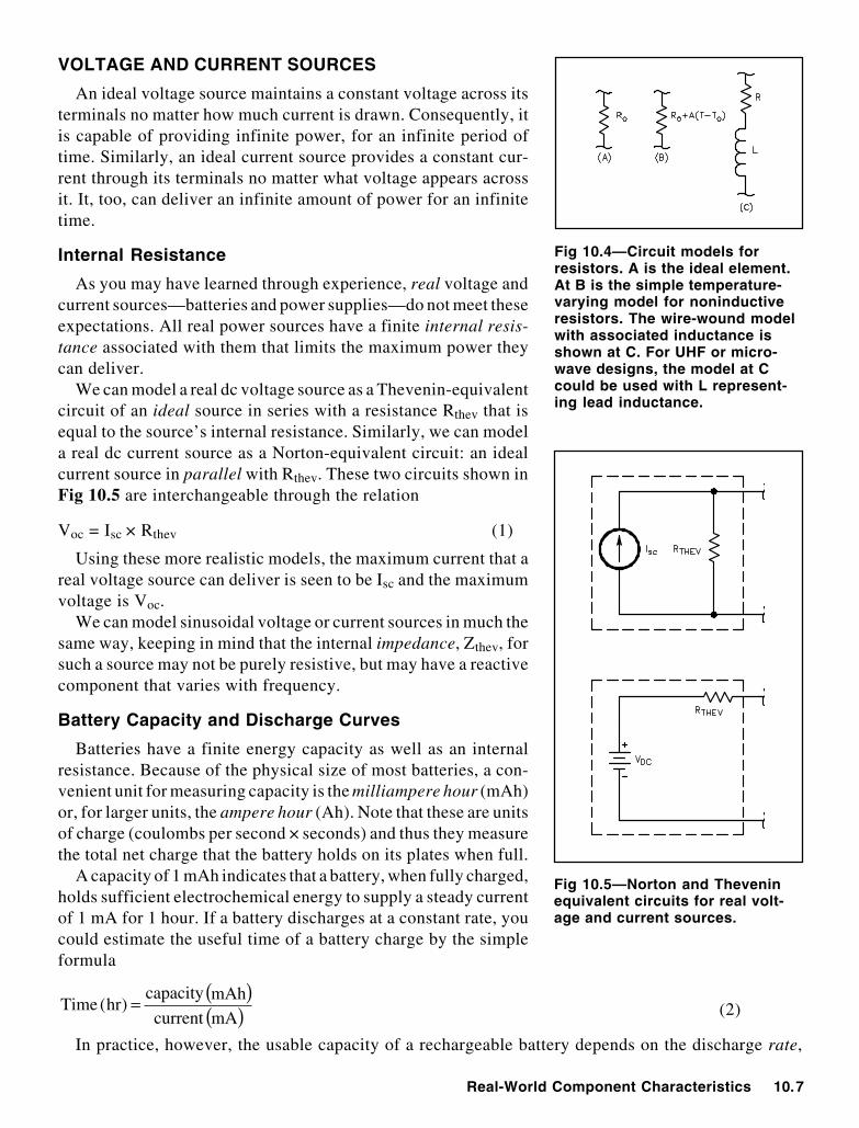
Another exception to the rule that resistors are, in general, fairly ideal has to do with skin effect at RF.This will be discussed later in the chapter. Fig 10.4 shows some more accurate circuit models for resistorsat low frequencies. For a treatment of pure resistance theory, look at the DC Theory chapter.
Table 10.1Temperature Coefficients forVarious ResistorCompositions1 PPM = 1 part per million = 0.0001%
Type TC (PPM/ °C)Wire wound ±(30 - 50)Metal Film ±(100 - 200)Carbon Film +350 to –800Carbon composition ±800
Real-World Component Characteristics 10.7
VOLTAGE AND CURRENT SOURCES
An ideal voltage source maintains a constant voltage across itsterminals no matter how much current is drawn. Consequently, itis capable of providing infinite power, for an infinite period oftime. Similarly, an ideal current source provides a constant cur-rent through its terminals no matter what voltage appears acrossit. It, too, can deliver an infinite amount of power for an infinitetime.
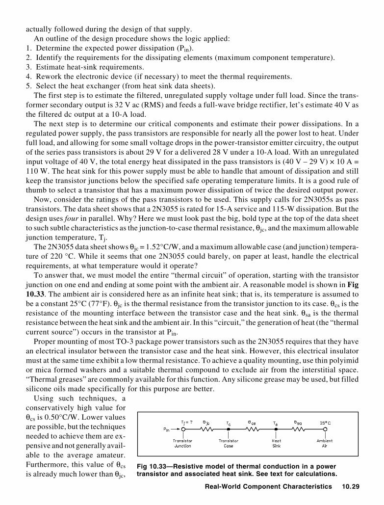
Internal Resistance
As you may have learned through experience, real voltage andcurrent sources—batteries and power supplies—do not meet theseexpectations. All real power sources have a finite internal resis-tance associated with them that limits the maximum power theycan deliver.
We can model a real dc voltage source as a Thevenin-equivalentcircuit of an ideal source in series with a resistance Rthev that isequal to the source’s internal resistance. Similarly, we can modela real dc current source as a Norton-equivalent circuit: an idealcurrent source in parallel with Rthev. These two circuits shown inFig 10.5 are interchangeable through the relation
Voc = Isc × Rthev (1)
Using these more realistic models, the maximum current that areal voltage source can deliver is seen to be Isc and the maximumvoltage is Voc.
We can model sinusoidal voltage or current sources in much thesame way, keeping in mind that the internal impedance, Zthev, forsuch a source may not be purely resistive, but may have a reactivecomponent that varies with frequency.
Battery Capacity and Discharge Curves
Batteries have a finite energy capacity as well as an internalresistance. Because of the physical size of most batteries, a con-venient unit for measuring capacity is the milliampere hour (mAh)or, for larger units, the ampere hour (Ah). Note that these are unitsof charge (coulombs per second × seconds) and thus they measurethe total net charge that the battery holds on its plates when full.
A capacity of 1 mAh indicates that a battery, when fully charged,holds sufficient electrochemical energy to supply a steady currentof 1 mA for 1 hour. If a battery discharges at a constant rate, youcould estimate the useful time of a battery charge by the simpleformula
( )( )mA current
mAhcapacity)hr(Time = (2)
In practice, however, the usable capacity of a rechargeable battery depends on the discharge rate,
Fig 10.5—Norton and Theveninequivalent circuits for real volt-age and current sources.
Fig 10.4—Circuit models forresistors. A is the ideal element.At B is the simple temperature-varying model for noninductiveresistors. The wire-wound modelwith associated inductance isshown at C. For UHF or micro-wave designs, the model at Ccould be used with L represent-ing lead inductance.
10.8 Chapter 10
decreasing slightly as the current increases. For example, a500 mAh nickel-cadmium (NiCd) battery may supply a current of50 mA for almost 10 hours while maintaining a current of 500 mAfor only 45 minutes.
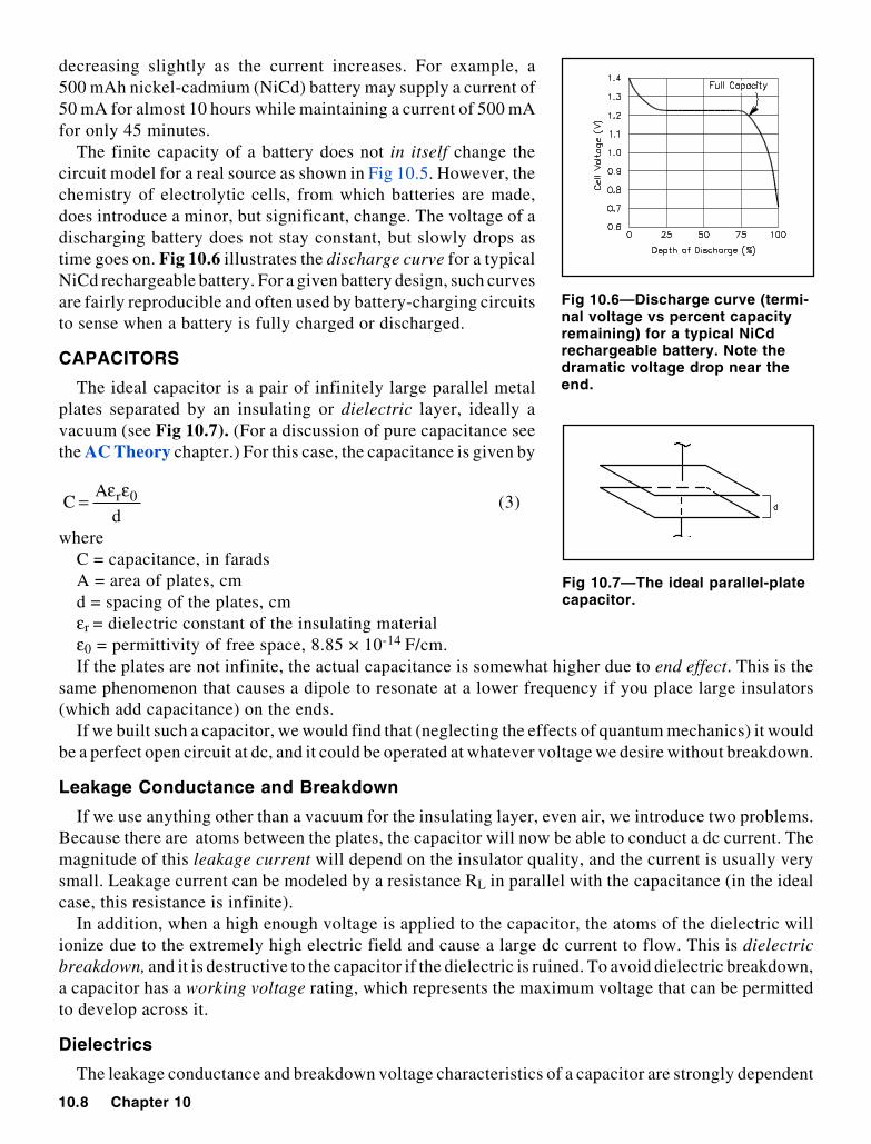
The finite capacity of a battery does not in itself change thecircuit model for a real source as shown in Fig 10.5. However, thechemistry of electrolytic cells, from which batteries are made,does introduce a minor, but significant, change. The voltage of adischarging battery does not stay constant, but slowly drops astime goes on. Fig 10.6 illustrates the discharge curve for a typicalNiCd rechargeable battery. For a given battery design, such curvesare fairly reproducible and often used by battery-charging circuitsto sense when a battery is fully charged or discharged.
CAPACITORS
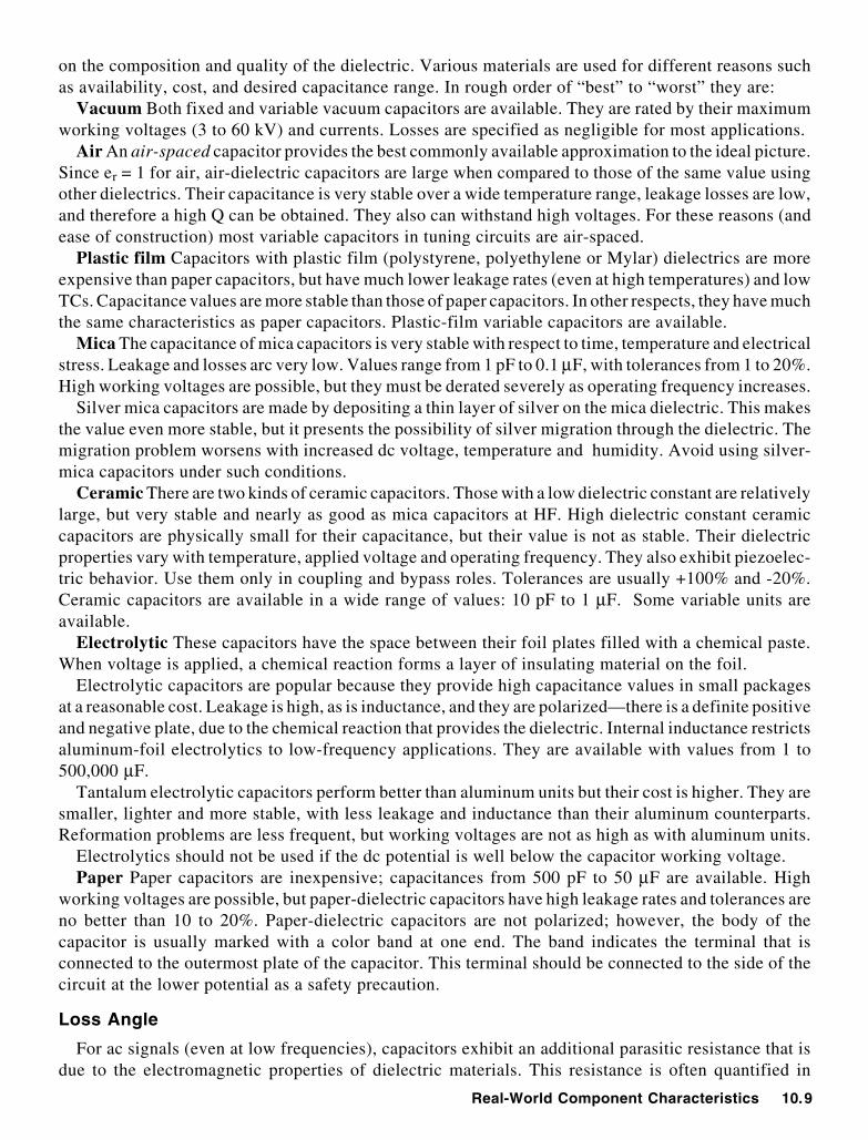
The ideal capacitor is a pair of infinitely large parallel metalplates separated by an insulating or dielectric layer, ideally avacuum (see Fig 10.7). (For a discussion of pure capacitance seethe AC Theory chapter.) For this case, the capacitance is given by
d
AC 0rεε= (3)
whereC = capacitance, in faradsA = area of plates, cmd = spacing of the plates, cmεr = dielectric constant of the insulating materialε0 = permittivity of free space, 8.85 × 10⁻¹⁴ F/cm.If the plates are not infinite, the actual capacitance is somewhat higher due to end effect. This is the
same phenomenon that causes a dipole to resonate at a lower frequency if you place large insulators(which add capacitance) on the ends.
If we built such a capacitor, we would find that (neglecting the effects of quantum mechanics) it wouldbe a perfect open circuit at dc, and it could be operated at whatever voltage we desire without breakdown.
Leakage Conductance and Breakdown
If we use anything other than a vacuum for the insulating layer, even air, we introduce two problems.Because there are atoms between the plates, the capacitor will now be able to conduct a dc current. Themagnitude of this leakage current will depend on the insulator quality, and the current is usually verysmall. Leakage current can be modeled by a resistance RL in parallel with the capacitance (in the idealcase, this resistance is infinite).
In addition, when a high enough voltage is applied to the capacitor, the atoms of the dielectric willionize due to the extremely high electric field and cause a large dc current to flow. This is dielectricbreakdown, and it is destructive to the capacitor if the dielectric is ruined. To avoid dielectric breakdown,a capacitor has a working voltage rating, which represents the maximum voltage that can be permittedto develop across it.
Dielectrics
The leakage conductance and breakdown voltage characteristics of a capacitor are strongly dependent
Fig 10.7—The ideal parallel-platecapacitor.
Fig 10.6—Discharge curve (termi-nal voltage vs percent capacityremaining) for a typical NiCdrechargeable battery. Note thedramatic voltage drop near theend.
Real-World Component Characteristics 10.9
on the composition and quality of the dielectric. Various materials are used for different reasons suchas availability, cost, and desired capacitance range. In rough order of “best” to “worst” they are:
Vacuum Both fixed and variable vacuum capacitors are available. They are rated by their maximumworking voltages (3 to 60 kV) and currents. Losses are specified as negligible for most applications.
Air An air-spaced capacitor provides the best commonly available approximation to the ideal picture.Since er = 1 for air, air-dielectric capacitors are large when compared to those of the same value usingother dielectrics. Their capacitance is very stable over a wide temperature range, leakage losses are low,and therefore a high Q can be obtained. They also can withstand high voltages. For these reasons (andease of construction) most variable capacitors in tuning circuits are air-spaced.
Plastic film Capacitors with plastic film (polystyrene, polyethylene or Mylar) dielectrics are moreexpensive than paper capacitors, but have much lower leakage rates (even at high temperatures) and lowTCs. Capacitance values are more stable than those of paper capacitors. In other respects, they have muchthe same characteristics as paper capacitors. Plastic-film variable capacitors are available.
Mica The capacitance of mica capacitors is very stable with respect to time, temperature and electricalstress. Leakage and losses arc very low. Values range from 1 pF to 0.1 µF, with tolerances from 1 to 20%.High working voltages are possible, but they must be derated severely as operating frequency increases.
Silver mica capacitors are made by depositing a thin layer of silver on the mica dielectric. This makesthe value even more stable, but it presents the possibility of silver migration through the dielectric. Themigration problem worsens with increased dc voltage, temperature and humidity. Avoid using silver-mica capacitors under such conditions.
Ceramic There are two kinds of ceramic capacitors. Those with a low dielectric constant are relativelylarge, but very stable and nearly as good as mica capacitors at HF. High dielectric constant ceramiccapacitors are physically small for their capacitance, but their value is not as stable. Their dielectricproperties vary with temperature, applied voltage and operating frequency. They also exhibit piezoelec-tric behavior. Use them only in coupling and bypass roles. Tolerances are usually +100% and -20%.Ceramic capacitors are available in a wide range of values: 10 pF to 1 µF. Some variable units areavailable.
Electrolytic These capacitors have the space between their foil plates filled with a chemical paste.When voltage is applied, a chemical reaction forms a layer of insulating material on the foil.
Electrolytic capacitors are popular because they provide high capacitance values in small packagesat a reasonable cost. Leakage is high, as is inductance, and they are polarized—there is a definite positiveand negative plate, due to the chemical reaction that provides the dielectric. Internal inductance restrictsaluminum-foil electrolytics to low-frequency applications. They are available with values from 1 to500,000 µF.
Tantalum electrolytic capacitors perform better than aluminum units but their cost is higher. They aresmaller, lighter and more stable, with less leakage and inductance than their aluminum counterparts.Reformation problems are less frequent, but working voltages are not as high as with aluminum units.
Electrolytics should not be used if the dc potential is well below the capacitor working voltage.Paper Paper capacitors are inexpensive; capacitances from 500 pF to 50 µF are available. High
working voltages are possible, but paper-dielectric capacitors have high leakage rates and tolerances areno better than 10 to 20%. Paper-dielectric capacitors are not polarized; however, the body of thecapacitor is usually marked with a color band at one end. The band indicates the terminal that isconnected to the outermost plate of the capacitor. This terminal should be connected to the side of thecircuit at the lower potential as a safety precaution.
Loss Angle
For ac signals (even at low frequencies), capacitors exhibit an additional parasitic resistance that isdue to the electromagnetic properties of dielectric materials. This resistance is often quantified in
10.10 Chapter 10
Fig 10.8—A simple capacitormodel for frequencies well belowself-resonance.
catalogs as loss angle, θ, because it represents the angle, in thecomplex impedance plane, between ZC = R + jXC and XC. Thisangle is usually quite small, and would be zero for an ideal capaci-tor.
Loss angle is normally specified as tan θ at a certain frequency,which is simply the ratio R/XC. The loss angle of a given capacitoris relatively constant over frequency, which means the effectiveseries resistance or ESR = (tan θ) / (2 π f C) goes down as fre-quency goes up. This resistance is placed in series with the capaci-tor because it came (mathematically) from the equation for ZC
above. It can always be converted into a parallel resistance ifdesired. To summarize, Figs 10.8 and 10.9 show reasonable mod-els for the capacitor that are good up to VHF.
Temperature Coefficients and Tolerances
As with resistors, capacitor values vary in production, and mostcapacitors have a tolerance rating either printed on them or listedon a data sheet. Capacitance varies with temperature, and this isimportant to consider when constructing a circuit that will carryhigh power levels or operate in a hot environment. Also, as justdescribed, not all capacitors are available in all ranges of valuesdue to inherent differences in material properties. Typical values,temperature coefficients and leakage conductances for severalcapacitor types are given in Table 10.2.
DIODES
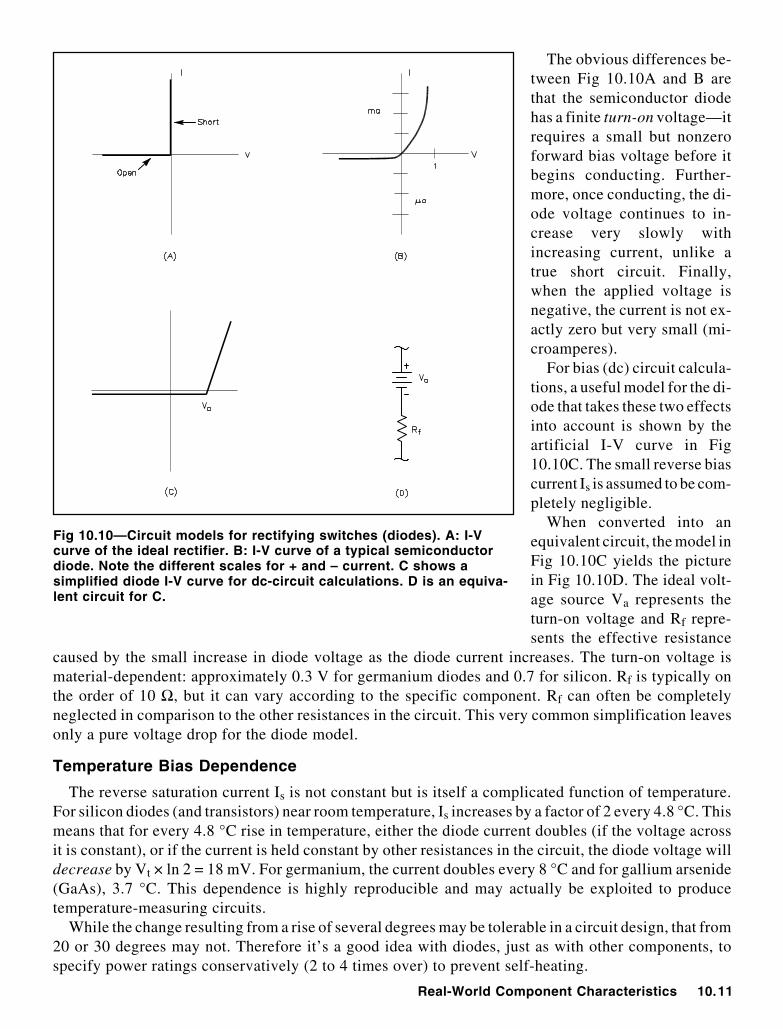
An ideal diode acts as a rectifying switch—it is a short circuitwhen forward biased and an open circuit when reverse biased.Many circuit components can be completely described in terms ofcurrent-voltage (or I-V ) characteristics, and to discuss the diode,this approach is especially helpful. Fig 10.10A shows the I-Vcurve for an ideal rectifier.
In contrast, the I-V curve for a semiconductor diode junction isgiven by the following equation (slightly simplified).
= tv
v
s eII (4)
whereI = diode currentV = diode voltageIs = reverse-bias saturation
currentVt = kT/q, the thermal equiva-
lent of voltage (about 25mV at room temperature).
This curve is shown in Fig10.10B.
Fig 10.9—A capacitor model forVHF and above including seriesresistance and distributed induc-tance.
Table 10.2Typical Temperature Coefficients and Leakage Conductancesfor Various Capacitor Constructions
Type TC @ 20°C DC Leakage (PPM/°C) Conductance (Ω)
Ceramic Disc ±300(NP0) > 10 M+150/–1500(GP) > 10 M
Mica –20 to +100 > 100,000 MPolyester ±500 > 10 MTantalum Electrolytic ±1500 > 10 MΩSmall Al Electrolytic(≈ 100 µF) –20,000 500 k - 1 MLarge Al Electrolytic(≈ 10 mF) –100,000 10 kVacuum (glass) +100 ≈ ∞Vacuum (ceramic) +50 ≈ ∞
Real-World Component Characteristics 10.11
The obvious differences be-tween Fig 10.10A and B arethat the semiconductor diodehas a finite turn-on voltage—itrequires a small but nonzeroforward bias voltage before itbegins conducting. Further-more, once conducting, the di-ode voltage continues to in-crease very slowly withincreasing current, unlike atrue short circuit. Finally,when the applied voltage isnegative, the current is not ex-actly zero but very small (mi-croamperes).
For bias (dc) circuit calcula-tions, a useful model for the di-ode that takes these two effectsinto account is shown by theartificial I-V curve in Fig10.10C. The small reverse biascurrent Is is assumed to be com-pletely negligible.
When converted into anequivalent circuit, the model inFig 10.10C yields the picturein Fig 10.10D. The ideal volt-age source Va represents theturn-on voltage and Rf repre-sents the effective resistance
caused by the small increase in diode voltage as the diode current increases. The turn-on voltage ismaterial-dependent: approximately 0.3 V for germanium diodes and 0.7 for silicon. Rf is typically onthe order of 10 Ω, but it can vary according to the specific component. Rf can often be completelyneglected in comparison to the other resistances in the circuit. This very common simplification leavesonly a pure voltage drop for the diode model.
Temperature Bias Dependence
The reverse saturation current Is is not constant but is itself a complicated function of temperature.For silicon diodes (and transistors) near room temperature, Is increases by a factor of 2 every 4.8 °C. Thismeans that for every 4.8 °C rise in temperature, either the diode current doubles (if the voltage acrossit is constant), or if the current is held constant by other resistances in the circuit, the diode voltage willdecrease by Vt × ln 2 = 18 mV. For germanium, the current doubles every 8 °C and for gallium arsenide(GaAs), 3.7 °C. This dependence is highly reproducible and may actually be exploited to producetemperature-measuring circuits.
While the change resulting from a rise of several degrees may be tolerable in a circuit design, that from20 or 30 degrees may not. Therefore it’s a good idea with diodes, just as with other components, tospecify power ratings conservatively (2 to 4 times over) to prevent self-heating.
Fig 10.10—Circuit models for rectifying switches (diodes). A: I-Vcurve of the ideal rectifier. B: I-V curve of a typical semiconductordiode. Note the different scales for + and – current. C shows asimplified diode I-V curve for dc-circuit calculations. D is an equiva-lent circuit for C.
10.12 Chapter 10
While component derating does reduce self-heating effects, circuits must be designed for the expectedoperating environment. For example, mobile radios may face temperatures from –20° to +140°F (–29°to 60°C).
Junction Capacitance
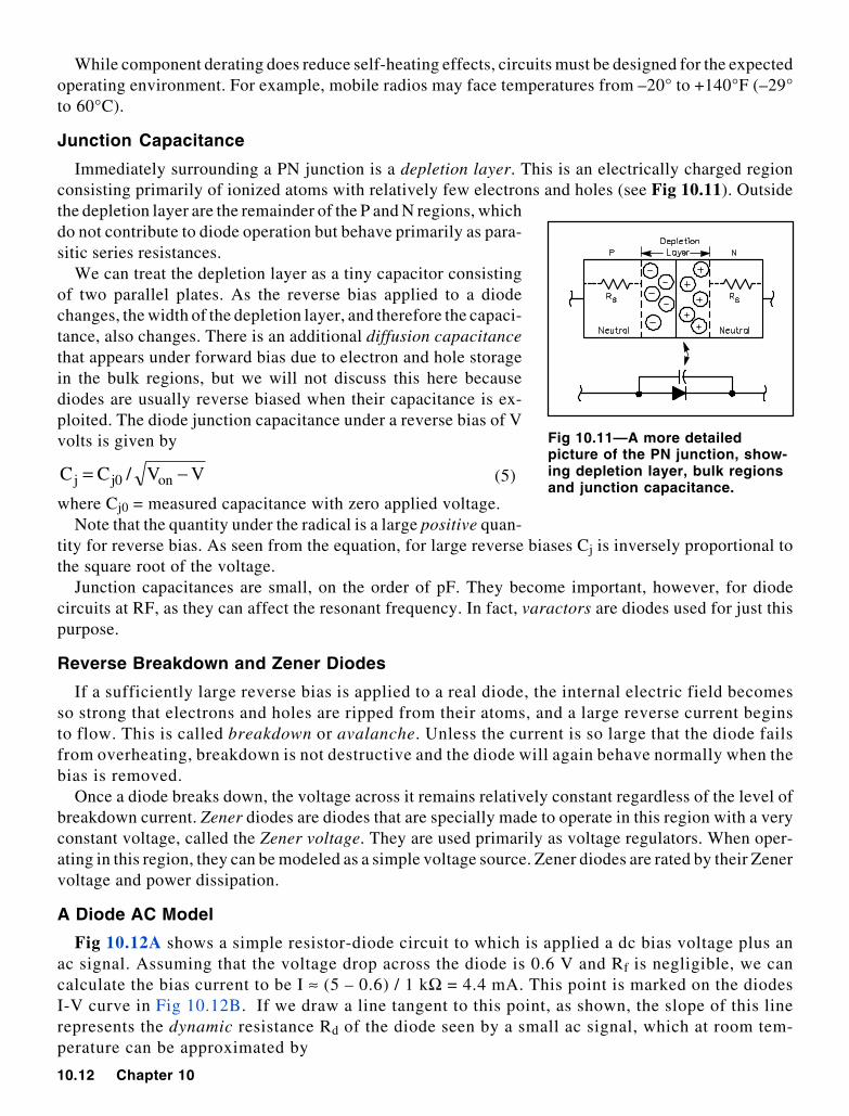
Immediately surrounding a PN junction is a depletion layer. This is an electrically charged regionconsisting primarily of ionized atoms with relatively few electrons and holes (see Fig 10.11). Outsidethe depletion layer are the remainder of the P and N regions, whichdo not contribute to diode operation but behave primarily as para-sitic series resistances.
We can treat the depletion layer as a tiny capacitor consistingof two parallel plates. As the reverse bias applied to a diodechanges, the width of the depletion layer, and therefore the capaci-tance, also changes. There is an additional diffusion capacitancethat appears under forward bias due to electron and hole storagein the bulk regions, but we will not discuss this here becausediodes are usually reverse biased when their capacitance is ex-ploited. The diode junction capacitance under a reverse bias of Vvolts is given by
VV/CC on0jj −= (5)
where Cj0 = measured capacitance with zero applied voltage.Note that the quantity under the radical is a large positive quan-
tity for reverse bias. As seen from the equation, for large reverse biases Cj is inversely proportional tothe square root of the voltage.
Junction capacitances are small, on the order of pF. They become important, however, for diodecircuits at RF, as they can affect the resonant frequency. In fact, varactors are diodes used for just thispurpose.
Reverse Breakdown and Zener Diodes
If a sufficiently large reverse bias is applied to a real diode, the internal electric field becomesso strong that electrons and holes are ripped from their atoms, and a large reverse current beginsto flow. This is called breakdown or avalanche. Unless the current is so large that the diode failsfrom overheating, breakdown is not destructive and the diode will again behave normally when thebias is removed.
Once a diode breaks down, the voltage across it remains relatively constant regardless of the level ofbreakdown current. Zener diodes are diodes that are specially made to operate in this region with a veryconstant voltage, called the Zener voltage. They are used primarily as voltage regulators. When oper-ating in this region, they can be modeled as a simple voltage source. Zener diodes are rated by their Zenervoltage and power dissipation.
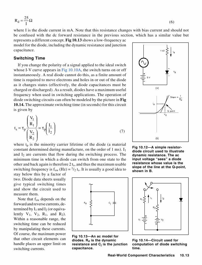
A Diode AC Model
Fig 10.12A shows a simple resistor-diode circuit to which is applied a dc bias voltage plus anac signal. Assuming that the voltage drop across the diode is 0.6 V and Rf is negligible, we cancalculate the bias current to be I ≈ (5 – 0.6) / 1 kΩ = 4.4 mA. This point is marked on the diodesI-V curve in Fig 10.12B. If we draw a line tangent to this point, as shown, the slope of this linerepresents the dynamic resistance Rd of the diode seen by a small ac signal, which at room tem-perature can be approximated by
Fig 10.11—A more detailedpicture of the PN junction, show-ing depletion layer, bulk regionsand junction capacitance.
Real-World Component Characteristics 10.13
Ω=I
25Rd (6)
where I is the diode current in mA. Note that this resistance changes with bias current and should notbe confused with the dc forward resistance in the previous section, which has a similar value butrepresents a different concept. Fig 10.13 shows a low-frequency acmodel for the diode, including the dynamic resistance and junctioncapacitance.
Switching Time
If you change the polarity of a signal applied to the ideal switchwhose I-V curve appears in Fig 10.10A, the switch turns on or offinstantaneously. A real diode cannot do this, as a finite amount oftime is required to move electrons and holes in or out of the diodeas it changes states (effectively, the diode capacitances must becharged or discharged). As a result, diodes have a maximum usefulfrequency when used in switching applications. The operation ofdiode switching circuits can often be modeled by the picture in Fig10.14. The approximate switching time (in seconds) for this circuitis given by
τ=
τ=2
1p
2
2
1
1
ps II
RV
RV
t(7)
where tp is the minority carrier lifetime of the diode (a materialconstant determined during manufacture, on the order of 1 ms). I1
and I2 are currents that flow during the switching process. Theminimum time in which a diode can switch from one state to theother and back again is therefore 2 ts, and thus the maximum usableswitching frequency is fsw (Hz) = 1/2 ts. It is usually a good idea tostay below this by a factor oftwo. Diode data sheets usuallygive typical switching timesand show the circuit used tomeasure them.
Note that fsw depends on theforward and reverse currents, de-termined by I1 and I2 (or equiva-lently V1, V2, R1, and R2).Within a reasonable range, theswitching time can be reducedby manipulating these currents.Of course, the maximum powerthat other circuit elements canhandle places an upper limit onswitching currents.
Fig 10.12—A simple resistor-diode circuit used to illustratedynamic resistance. The acinput voltage “sees” a dioderesistance whose value is theslope of the line at the Q-point,shown in B.
Fig 10.14—Circuit used forcomputation of diode switchingtime.
Fig 10.13—An ac model fordiodes. Rd is the dynamicresistance and Cj is the junctioncapacitance.
10.14 Chapter 10
Schottky Diodes
Schottky diodes are made from metal-semiconductor junctions rather than PN junctions. They storeless charge internally and as a result, have shorter switching times and junction capacitances thanstandard PN junction diodes.
Their turn-on voltage is also less, typically 0.3 to 0.4 V. In most other respects they behave similarlyto PN diodes.
INDUCTORS
Inductors are the problem children of the component world. (Fundamental inductance is discussed inthe AC Theory chapter.) Besides being difficult to fabricate on integrated circuits, they are perhaps themost nonideal of real-world components. While the leakage conductance of a capacitor is usuallynegligible, the series resistance of an inductor often is not. This is basically because an inductor is madeof a long piece of relatively thin wire wound into a small coil. As an example, consider a typical air-coretuning coil from a component catalog, with L = 33 µH and a minimum Q of 30 measured at 2.5 MHz.This would indicate a series resistance of Rs = 2 π f L / Q = 17 Ω. This Rs could significantly alter theresonant frequency of a circuit. For frequencies up to HF this is the only significant nonlinearity, anda low-frequency circuit model for the inductor is shown in Fig 10.15. Many of the problems associatedwith inductors are actually due to core materials, and not the coilitself.
Magnetic Materials
Many discrete inductors and transformers are wound on a coreof iron or other magnetic material. As discussed in the AC Theorychapter, the inductance value of a coil is proportional to the den-sity of magnetic field lines that pass through it. A piece of mag-netic material placed inside a coil will concentrate the field linesinside itself. This permits a higher number of field lines to existinside a coil of a given cross-sectional area, thus allowing a muchhigher inductance than what would be possible with an air core.This is especially important for transformers that operate at lowfrequencies (such as 60 Hz) to ensure the reactance of the wind-ings is high.
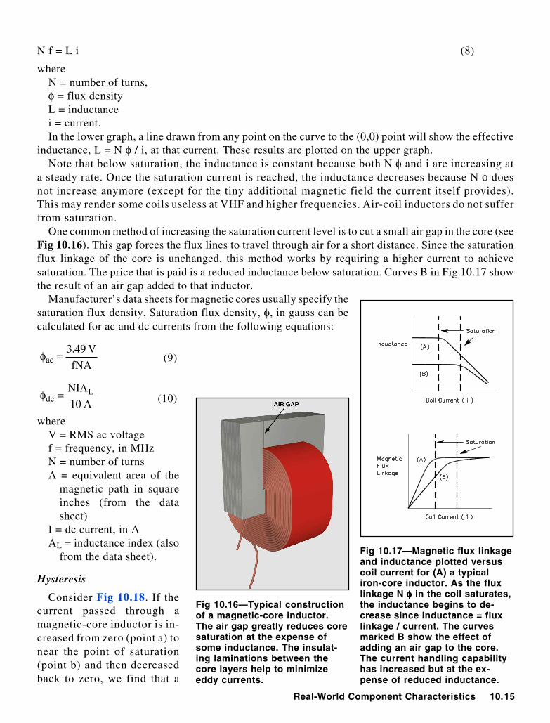
Core Saturation
Magnetic (more precisely, ferromagnetic) materials exhibit two kinds of nonlinear behavior that areimportant to circuit design. The first is the phenomenon of saturation. A magnetic core increases themagnetic flux density of a coil because the current passing through the coil forces the atoms of the iron(or other material) to line up, just like many small compass needles, and the magnetic field that resultsfrom the atomic alignment is much larger than that produced by the current with no core. As coil currentincreases, more and more atoms line up. At some high current, all of the atoms will be aligned and thecore is saturated. Any further increase in current can’t increase the core alignment any further. Ofcourse, added current generates its own magnetic flux, but it is very small compared to the magnetic fieldcontributed by the aligned atoms in the magnetic core.
The important concept in terms of circuit design is that as long as the coil current remains belowsaturation, the inductance of the coil is essentially constant. Fig 10.17 shows graphs of magnetic fluxlinkage (N φ) and inductance (L) vs current (i) for a typical iron-core inductor. These quantities arerelated by the equation
Fig 10.15—Low- to mid-frequencyinductor equivalent circuit show-ing series resistance Rs.
Real-World Component Characteristics 10.15
N f = L i (8)
whereN = number of turns,φ = flux densityL = inductancei = current.In the lower graph, a line drawn from any point on the curve to the (0,0) point will show the effective
inductance, L = N φ / i, at that current. These results are plotted on the upper graph.Note that below saturation, the inductance is constant because both N φ and i are increasing at
a steady rate. Once the saturation current is reached, the inductance decreases because N φ doesnot increase anymore (except for the tiny additional magnetic field the current itself provides).This may render some coils useless at VHF and higher frequencies. Air-coil inductors do not sufferfrom saturation.
One common method of increasing the saturation current level is to cut a small air gap in the core (seeFig 10.16). This gap forces the flux lines to travel through air for a short distance. Since the saturationflux linkage of the core is unchanged, this method works by requiring a higher current to achievesaturation. The price that is paid is a reduced inductance below saturation. Curves B in Fig 10.17 showthe result of an air gap added to that inductor.
Manufacturer’s data sheets for magnetic cores usually specify thesaturation flux density. Saturation flux density, φ, in gauss can becalculated for ac and dc currents from the following equations:
fNA
V49.3ac =φ (9)
A10
NIALdc =φ (10)
whereV = RMS ac voltagef = frequency, in MHzN = number of turnsA = equivalent area of the
magnetic path in squareinches (from the datasheet)
I = dc current, in AAL = inductance index (also
from the data sheet).
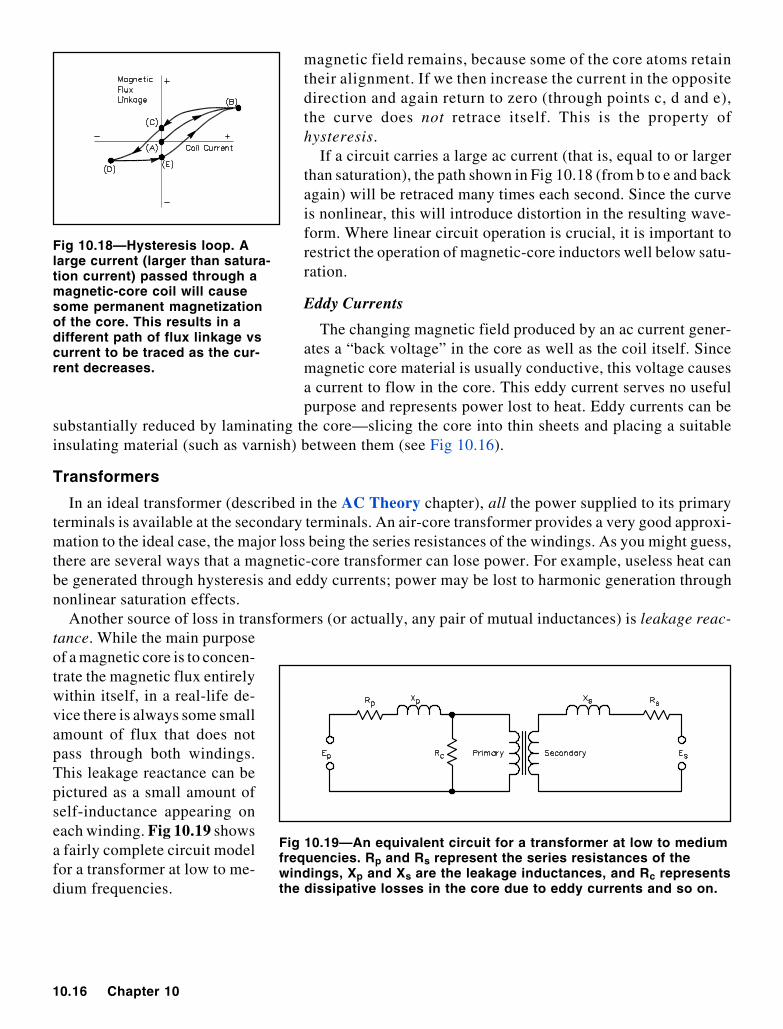
Hysteresis
Consider Fig 10.18. If thecurrent passed through amagnetic-core inductor is in-creased from zero (point a) tonear the point of saturation(point b) and then decreasedback to zero, we find that a
Fig 10.16—Typical constructionof a magnetic-core inductor.The air gap greatly reduces coresaturation at the expense ofsome inductance. The insulat-ing laminations between thecore layers help to minimizeeddy currents.
Fig 10.17—Magnetic flux linkageand inductance plotted versuscoil current for (A) a typicaliron-core inductor. As the fluxlinkage N φφφφφ in the coil saturates,the inductance begins to de-crease since inductance = fluxlinkage / current. The curvesmarked B show the effect ofadding an air gap to the core.The current handling capabilityhas increased but at the ex-pense of reduced inductance.
10.16 Chapter 10
magnetic field remains, because some of the core atoms retaintheir alignment. If we then increase the current in the oppositedirection and again return to zero (through points c, d and e),the curve does not retrace itself. This is the property ofhysteresis.
If a circuit carries a large ac current (that is, equal to or largerthan saturation), the path shown in Fig 10.18 (from b to e and backagain) will be retraced many times each second. Since the curveis nonlinear, this will introduce distortion in the resulting wave-form. Where linear circuit operation is crucial, it is important torestrict the operation of magnetic-core inductors well below satu-ration.
Eddy Currents
The changing magnetic field produced by an ac current gener-ates a “back voltage” in the core as well as the coil itself. Sincemagnetic core material is usually conductive, this voltage causesa current to flow in the core. This eddy current serves no usefulpurpose and represents power lost to heat. Eddy currents can be
substantially reduced by laminating the core—slicing the core into thin sheets and placing a suitableinsulating material (such as varnish) between them (see Fig 10.16).
Transformers
In an ideal transformer (described in the AC Theory chapter), all the power supplied to its primaryterminals is available at the secondary terminals. An air-core transformer provides a very good approxi-mation to the ideal case, the major loss being the series resistances of the windings. As you might guess,there are several ways that a magnetic-core transformer can lose power. For example, useless heat canbe generated through hysteresis and eddy currents; power may be lost to harmonic generation throughnonlinear saturation effects.
Another source of loss in transformers (or actually, any pair of mutual inductances) is leakage reac-tance. While the main purposeof a magnetic core is to concen-trate the magnetic flux entirelywithin itself, in a real-life de-vice there is always some smallamount of flux that does notpass through both windings.This leakage reactance can bepictured as a small amount ofself-inductance appearing oneach winding. Fig 10.19 showsa fairly complete circuit modelfor a transformer at low to me-dium frequencies.
Fig 10.18—Hysteresis loop. Alarge current (larger than satura-tion current) passed through amagnetic-core coil will causesome permanent magnetizationof the core. This results in adifferent path of flux linkage vscurrent to be traced as the cur-rent decreases.
Fig 10.19—An equivalent circuit for a transformer at low to mediumfrequencies. Rp and Rs represent the series resistances of thewindings, Xp and Xs are the leakage inductances, and Rc representsthe dissipative losses in the core due to eddy currents and so on.
Real-World Component Characteristics 10.17
The models described in the previous section are good for dc, and ac up through AF and low RF. AtHF and above (where we do much of our circuit design) several other considerations become veryimportant, in some cases dominant, in our component models. To understand what happens to circuitsat RF (a good cutoff is 30 MHz and above) we turn to a brief discussion of some electromagnetic andmicrowave theory concepts.
Parasitic Inductance
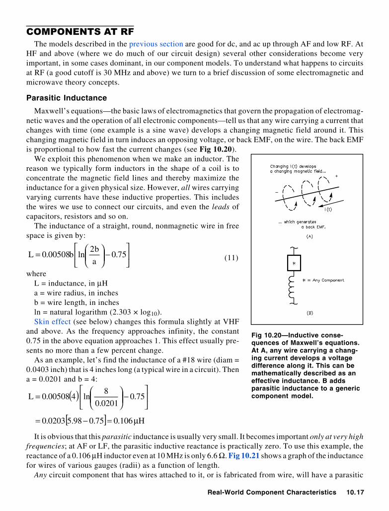
Maxwell’s equations—the basic laws of electromagnetics that govern the propagation of electromag-netic waves and the operation of all electronic components—tell us that any wire carrying a current thatchanges with time (one example is a sine wave) develops a changing magnetic field around it. Thischanging magnetic field in turn induces an opposing voltage, or back EMF, on the wire. The back EMFis proportional to how fast the current changes (see Fig 10.20).
We exploit this phenomenon when we make an inductor. Thereason we typically form inductors in the shape of a coil is toconcentrate the magnetic field lines and thereby maximize theinductance for a given physical size. However, all wires carryingvarying currents have these inductive properties. This includesthe wires we use to connect our circuits, and even the leads ofcapacitors, resistors and so on.
The inductance of a straight, round, nonmagnetic wire in freespace is given by:
−
= 75.0
a
b2lnb00508.0L (11)
whereL = inductance, in µHa = wire radius, in inchesb = wire length, in inchesln = natural logarithm (2.303 × log10).Skin effect (see below) changes this formula slightly at VHF
and above. As the frequency approaches infinity, the constant0.75 in the above equation approaches 1. This effect usually pre-sents no more than a few percent change.
As an example, let’s find the inductance of a #18 wire (diam =0.0403 inch) that is 4 inches long (a typical wire in a circuit). Thena = 0.0201 and b = 4:
( )
[ ] H106.075.098.50203.0
75.00201.0
8ln400508.0L
µ=−=
−
=
It is obvious that this parasitic inductance is usually very small. It becomes important only at very highfrequencies; at AF or LF, the parasitic inductive reactance is practically zero. To use this example, thereactance of a 0.106 µH inductor even at 10 MHz is only 6.6 Ω. Fig 10.21 shows a graph of the inductancefor wires of various gauges (radii) as a function of length.
Any circuit component that has wires attached to it, or is fabricated from wire, will have a parasitic
Fig 10.20—Inductive conse-quences of Maxwell’s equations.At A, any wire carrying a chang-ing current develops a voltagedifference along it. This can bemathematically described as aneffective inductance. B addsparasitic inductance to a genericcomponent model.
10.18 Chapter 10
inductance associated with it. We can treat this parasitic inductance in component models by adding aninductor of appropriate value in series with the component (since the wire lengths are in series with theelement). This (among other reasons) is why minimizing lead lengths and interconnecting wires be-comes very important when designing circuits for VHF and above.
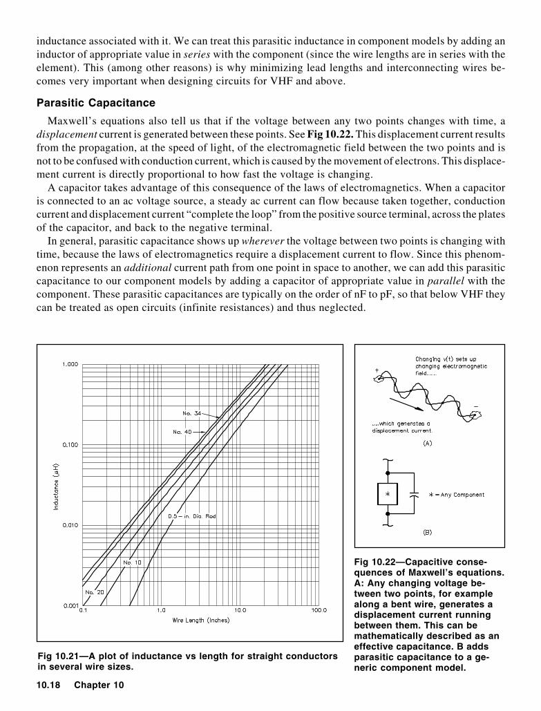
Parasitic Capacitance
Maxwell’s equations also tell us that if the voltage between any two points changes with time, adisplacement current is generated between these points. See Fig 10.22. This displacement current resultsfrom the propagation, at the speed of light, of the electromagnetic field between the two points and isnot to be confused with conduction current, which is caused by the movement of electrons. This displace-ment current is directly proportional to how fast the voltage is changing.
A capacitor takes advantage of this consequence of the laws of electromagnetics. When a capacitoris connected to an ac voltage source, a steady ac current can flow because taken together, conductioncurrent and displacement current “complete the loop” from the positive source terminal, across the platesof the capacitor, and back to the negative terminal.
In general, parasitic capacitance shows up wherever the voltage between two points is changing withtime, because the laws of electromagnetics require a displacement current to flow. Since this phenom-enon represents an additional current path from one point in space to another, we can add this parasiticcapacitance to our component models by adding a capacitor of appropriate value in parallel with thecomponent. These parasitic capacitances are typically on the order of nF to pF, so that below VHF theycan be treated as open circuits (infinite resistances) and thus neglected.
Fig 10.21—A plot of inductance vs length for straight conductorsin several wire sizes.
Fig 10.22—Capacitive conse-quences of Maxwell’s equations.A: Any changing voltage be-tween two points, for examplealong a bent wire, generates adisplacement current runningbetween them. This can bemathematically described as aneffective capacitance. B addsparasitic capacitance to a ge-neric component model.
Real-World Component Characteristics 10.19
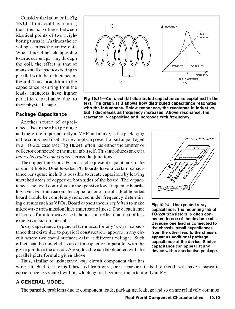
Consider the inductor in Fig10.23. If this coil has n turns,then the ac voltage betweenidentical points of two neigh-boring turns is 1/n times the acvoltage across the entire coil.When this voltage changes dueto an ac current passing throughthe coil, the effect is that ofmany small capacitors acting inparallel with the inductance ofthe coil. Thus, in addition to thecapacitance resulting from theleads, inductors have higherparasitic capacitance due totheir physical shape.
Package Capacitance
Another source of capaci-tance, also in the nF to pF rangeand therefore important only at VHF and above, is the packagingof the component itself. For example, a power transistor packagedin a TO-220 case (see Fig 10.24), often has either the emitter orcollector connected to the metal tab itself. This introduces an extrainter-electrode capacitance across the junctions.
The copper traces on a PC board also present capacitance to thecircuit it holds. Double-sided PC boards have a certain capaci-tance per square inch. It is possible to create capacitors by leavingunetched areas of copper on both sides of the board. The capaci-tance is not well controlled on inexpensive low-frequency boards,however. For this reason, the copper on one side of a double-sidedboard should be completely removed under frequency-determin-ing circuits such as VFOs. Board capacitance is exploited to makemicrowave transmission lines (microstrip lines). The capacitanceof boards for microwave use is better controlled than that of lessexpensive board material.
Stray capacitance (a general term used for any “extra” capaci-tance that exists due to physical construction) appears in any cir-cuit where two metal surfaces exist at different voltages. Sucheffects can be modeled as an extra capacitor in parallel with thegiven points in the circuit. A rough value can be obtained with theparallel-plate formula given above.
Thus, similar to inductance, any circuit component that haswires attached to it, or is fabricated from wire, or is near or attached to metal, will have a parasiticcapacitance associated with it, which again, becomes important only at RF.
A GENERAL MODEL
The parasitic problems due to component leads, packaging, leakage and so on are relatively common
Fig 10.23—Coils exhibit distributed capacitance as explained in thetext. The graph at B shows how distributed capacitance resonateswith the inductance. Below resonance, the reactance is inductive,but it decreases as frequency increases. Above resonance, thereactance is capacitive and increases with frequency.
Fig 10.24—Unexpected straycapacitance. The mounting tab ofTO-220 transistors is often con-nected to one of the device leads.Because one lead is connected tothe chassis, small capacitancesfrom the other lead to the chassisappear as additional packagecapacitance at the device. Similarcapacitance can appear at anydevice with a conductive package.
10.20 Chapter 10
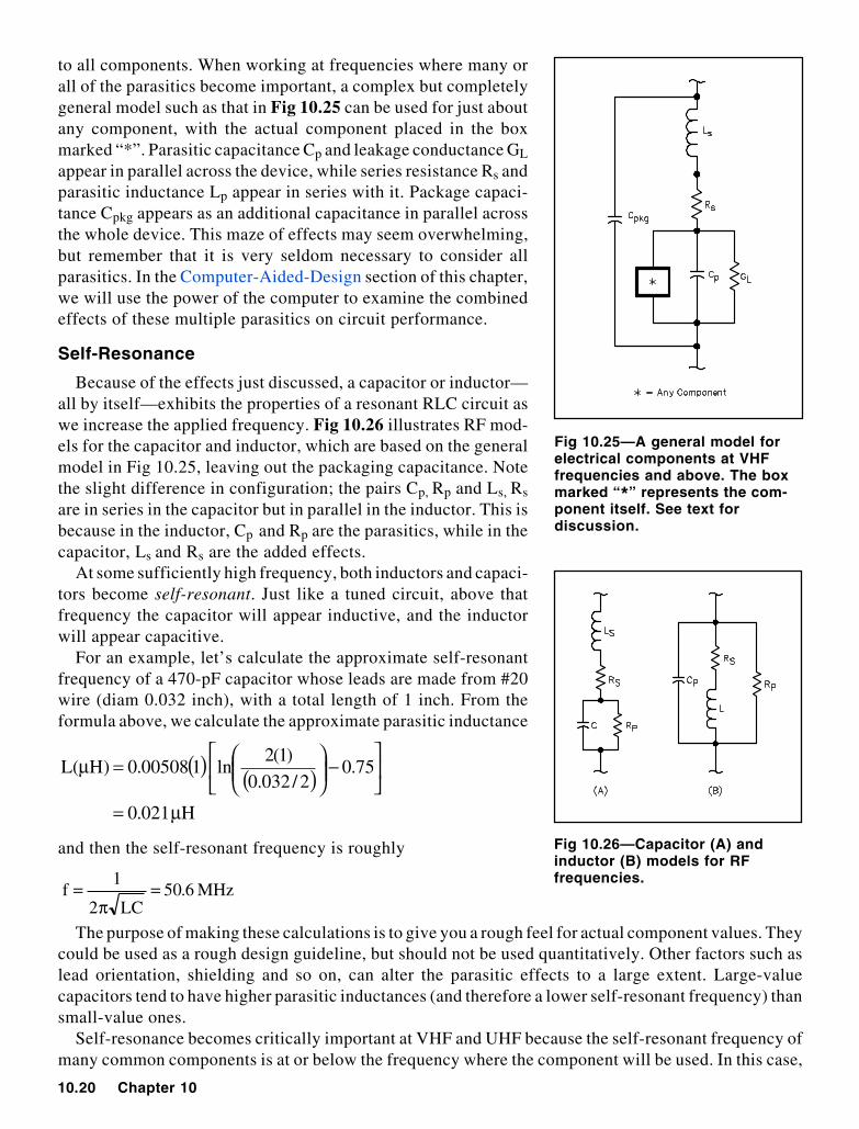
to all components. When working at frequencies where many orall of the parasitics become important, a complex but completelygeneral model such as that in Fig 10.25 can be used for just aboutany component, with the actual component placed in the boxmarked “*”. Parasitic capacitance Cp and leakage conductance GL
appear in parallel across the device, while series resistance Rs andparasitic inductance Lp appear in series with it. Package capaci-tance Cpkg appears as an additional capacitance in parallel acrossthe whole device. This maze of effects may seem overwhelming,but remember that it is very seldom necessary to consider allparasitics. In the Computer-Aided-Design section of this chapter,we will use the power of the computer to examine the combinedeffects of these multiple parasitics on circuit performance.
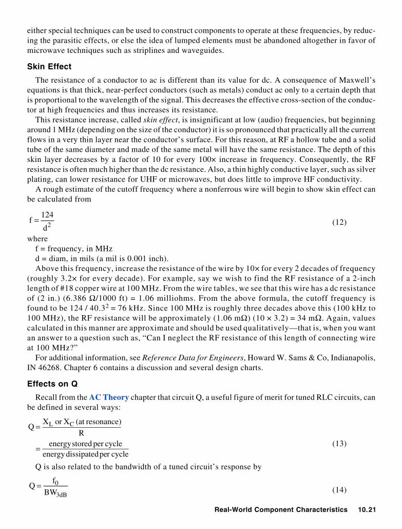
Self-Resonance
Because of the effects just discussed, a capacitor or inductor—all by itself—exhibits the properties of a resonant RLC circuit aswe increase the applied frequency. Fig 10.26 illustrates RF mod-els for the capacitor and inductor, which are based on the generalmodel in Fig 10.25, leaving out the packaging capacitance. Notethe slight difference in configuration; the pairs Cp, Rp and Ls, Rs
are in series in the capacitor but in parallel in the inductor. This isbecause in the inductor, Cp and Rp are the parasitics, while in thecapacitor, Ls and Rs are the added effects.
At some sufficiently high frequency, both inductors and capaci-tors become self-resonant. Just like a tuned circuit, above thatfrequency the capacitor will appear inductive, and the inductorwill appear capacitive.
For an example, let’s calculate the approximate self-resonantfrequency of a 470-pF capacitor whose leads are made from #20wire (diam 0.032 inch), with a total length of 1 inch. From theformula above, we calculate the approximate parasitic inductance
( ) ( )H021.0
75.02/032.0
)1(2ln100508.0)H(L
µ=
−
=µ
and then the self-resonant frequency is roughly
MHz6.50LC2
1f =
π=
The purpose of making these calculations is to give you a rough feel for actual component values. Theycould be used as a rough design guideline, but should not be used quantitatively. Other factors such aslead orientation, shielding and so on, can alter the parasitic effects to a large extent. Large-valuecapacitors tend to have higher parasitic inductances (and therefore a lower self-resonant frequency) thansmall-value ones.
Self-resonance becomes critically important at VHF and UHF because the self-resonant frequency ofmany common components is at or below the frequency where the component will be used. In this case,
Fig 10.25—A general model forelectrical components at VHFfrequencies and above. The boxmarked “*” represents the com-ponent itself. See text fordiscussion.
Fig 10.26—Capacitor (A) andinductor (B) models for RFfrequencies.
Real-World Component Characteristics 10.21
either special techniques can be used to construct components to operate at these frequencies, by reduc-ing the parasitic effects, or else the idea of lumped elements must be abandoned altogether in favor ofmicrowave techniques such as striplines and waveguides.
Skin Effect
The resistance of a conductor to ac is different than its value for dc. A consequence of Maxwell’sequations is that thick, near-perfect conductors (such as metals) conduct ac only to a certain depth thatis proportional to the wavelength of the signal. This decreases the effective cross-section of the conduc-tor at high frequencies and thus increases its resistance.
This resistance increase, called skin effect, is insignificant at low (audio) frequencies, but beginningaround 1 MHz (depending on the size of the conductor) it is so pronounced that practically all the currentflows in a very thin layer near the conductor’s surface. For this reason, at RF a hollow tube and a solidtube of the same diameter and made of the same metal will have the same resistance. The depth of thisskin layer decreases by a factor of 10 for every 100× increase in frequency. Consequently, the RFresistance is often much higher than the dc resistance. Also, a thin highly conductive layer, such as silverplating, can lower resistance for UHF or microwaves, but does little to improve HF conductivity.
A rough estimate of the cutoff frequency where a nonferrous wire will begin to show skin effect canbe calculated from
2d
124f = (12)
wheref = frequency, in MHzd = diam, in mils (a mil is 0.001 inch).Above this frequency, increase the resistance of the wire by 10× for every 2 decades of frequency
(roughly 3.2× for every decade). For example, say we wish to find the RF resistance of a 2-inchlength of #18 copper wire at 100 MHz. From the wire tables, we see that this wire has a dc resistanceof (2 in.) (6.386 Ω/1000 ft) = 1.06 milliohms. From the above formula, the cutoff frequency isfound to be 124 / 40.32 = 76 kHz. Since 100 MHz is roughly three decades above this (100 kHz to100 MHz), the RF resistance will be approximately (1.06 mΩ) (10 × 3.2) = 34 mΩ. Again, valuescalculated in this manner are approximate and should be used qualitatively—that is, when you wantan answer to a question such as, “Can I neglect the RF resistance of this length of connecting wireat 100 MHz?”
For additional information, see Reference Data for Engineers, Howard W. Sams & Co, Indianapolis,IN 46268. Chapter 6 contains a discussion and several design charts.
Effects on Q
Recall from the AC Theory chapter that circuit Q, a useful figure of merit for tuned RLC circuits, canbe defined in several ways:
cycle rpe dissipated energycycleper stored energy
R
resonance)(at Xor XQ CL
=
=
(13)
Q is also related to the bandwidth of a tuned circuit’s response by
dB3
0
BW
fQ = (14)
10.22 Chapter 10
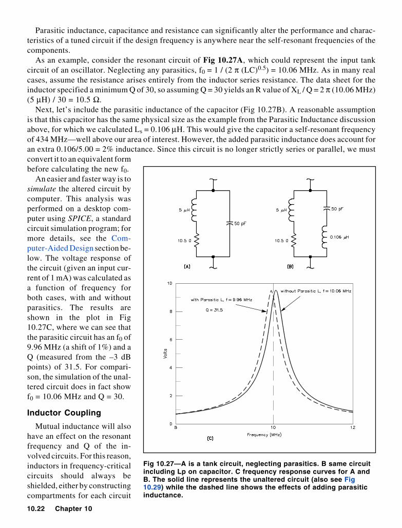
Parasitic inductance, capacitance and resistance can significantly alter the performance and charac-teristics of a tuned circuit if the design frequency is anywhere near the self-resonant frequencies of thecomponents.
As an example, consider the resonant circuit of Fig 10.27A, which could represent the input tankcircuit of an oscillator. Neglecting any parasitics, f0 = 1 / (2 π (LC)0.5) = 10.06 MHz. As in many realcases, assume the resistance arises entirely from the inductor series resistance. The data sheet for theinductor specified a minimum Q of 30, so assuming Q = 30 yields an R value of XL / Q = 2 π (10.06 MHz)(5 µH) / 30 = 10.5 Ω.
Next, let’s include the parasitic inductance of the capacitor (Fig 10.27B). A reasonable assumptionis that this capacitor has the same physical size as the example from the Parasitic Inductance discussionabove, for which we calculated Ls = 0.106 µH. This would give the capacitor a self-resonant frequencyof 434 MHz—well above our area of interest. However, the added parasitic inductance does account foran extra 0.106/5.00 = 2% inductance. Since this circuit is no longer strictly series or parallel, we mustconvert it to an equivalent formbefore calculating the new f0.
An easier and faster way is tosimulate the altered circuit bycomputer. This analysis wasperformed on a desktop com-puter using SPICE, a standardcircuit simulation program; formore details, see the Com-puter-Aided Design section be-low. The voltage response ofthe circuit (given an input cur-rent of 1 mA) was calculated asa function of frequency forboth cases, with and withoutparasitics. The results areshown in the plot in Fig10.27C, where we can see thatthe parasitic circuit has an f0 of9.96 MHz (a shift of 1%) and aQ (measured from the –3 dBpoints) of 31.5. For compari-son, the simulation of the unal-tered circuit does in fact showf0 = 10.06 MHz and Q = 30.
Inductor Coupling
Mutual inductance will alsohave an effect on the resonantfrequency and Q of the in-volved circuits. For this reason,inductors in frequency-criticalcircuits should always beshielded, either by constructingcompartments for each circuit
Fig 10.27—A is a tank circuit, neglecting parasitics. B same circuitincluding Lp on capacitor. C frequency response curves for A andB. The solid line represents the unaltered circuit (also see Fig10.29) while the dashed line shows the effects of adding parasiticinductance.
Real-World Component Characteristics 10.23
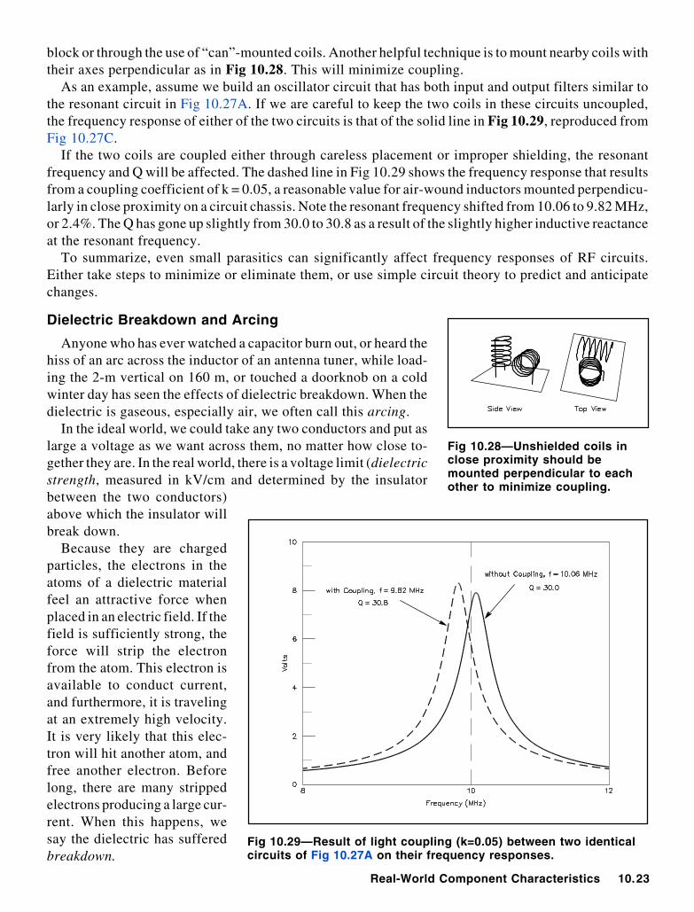
block or through the use of “can”-mounted coils. Another helpful technique is to mount nearby coils withtheir axes perpendicular as in Fig 10.28. This will minimize coupling.
As an example, assume we build an oscillator circuit that has both input and output filters similar tothe resonant circuit in Fig 10.27A. If we are careful to keep the two coils in these circuits uncoupled,the frequency response of either of the two circuits is that of the solid line in Fig 10.29, reproduced fromFig 10.27C.
If the two coils are coupled either through careless placement or improper shielding, the resonantfrequency and Q will be affected. The dashed line in Fig 10.29 shows the frequency response that resultsfrom a coupling coefficient of k = 0.05, a reasonable value for air-wound inductors mounted perpendicu-larly in close proximity on a circuit chassis. Note the resonant frequency shifted from 10.06 to 9.82 MHz,or 2.4%. The Q has gone up slightly from 30.0 to 30.8 as a result of the slightly higher inductive reactanceat the resonant frequency.
To summarize, even small parasitics can significantly affect frequency responses of RF circuits.Either take steps to minimize or eliminate them, or use simple circuit theory to predict and anticipatechanges.
Dielectric Breakdown and Arcing
Anyone who has ever watched a capacitor burn out, or heard thehiss of an arc across the inductor of an antenna tuner, while load-ing the 2-m vertical on 160 m, or touched a doorknob on a coldwinter day has seen the effects of dielectric breakdown. When thedielectric is gaseous, especially air, we often call this arcing.
In the ideal world, we could take any two conductors and put aslarge a voltage as we want across them, no matter how close to-gether they are. In the real world, there is a voltage limit (dielectricstrength, measured in kV/cm and determined by the insulatorbetween the two conductors)above which the insulator willbreak down.
Because they are chargedparticles, the electrons in theatoms of a dielectric materialfeel an attractive force whenplaced in an electric field. If thefield is sufficiently strong, theforce will strip the electronfrom the atom. This electron isavailable to conduct current,and furthermore, it is travelingat an extremely high velocity.It is very likely that this elec-tron will hit another atom, andfree another electron. Beforelong, there are many strippedelectrons producing a large cur-rent. When this happens, wesay the dielectric has sufferedbreakdown.
Fig 10.28—Unshielded coils inclose proximity should bemounted perpendicular to eachother to minimize coupling.
Fig 10.29—Result of light coupling (k=0.05) between two identicalcircuits of Fig 10.27A on their frequency responses.
10.24 Chapter 10
If the dielectric is liquid or gas, it can heal when the applied voltage is removed. A solid dielectric,however, cannot repair itself. A good example of this is a CMOS integrated circuit. When exposed tothe very high voltages associated with static electricity, the electric field across the very thin gate oxidelayer exceeds the dielectric strength of silicon dioxide, and the device is permanently damaged.
Capacitors are, by nature, perhaps the component most often associated with dielectric failure. Toprevent damage, the working voltage of a capacitor—and there are separate dc and ac ratings—shouldideally be 2 or 3 times the expected maximum voltage in the circuit.
Arcing is most often seen in RF circuits where the voltages are normally high, but it is possibleanywhere two components at significantly different voltage levels are closely spaced.
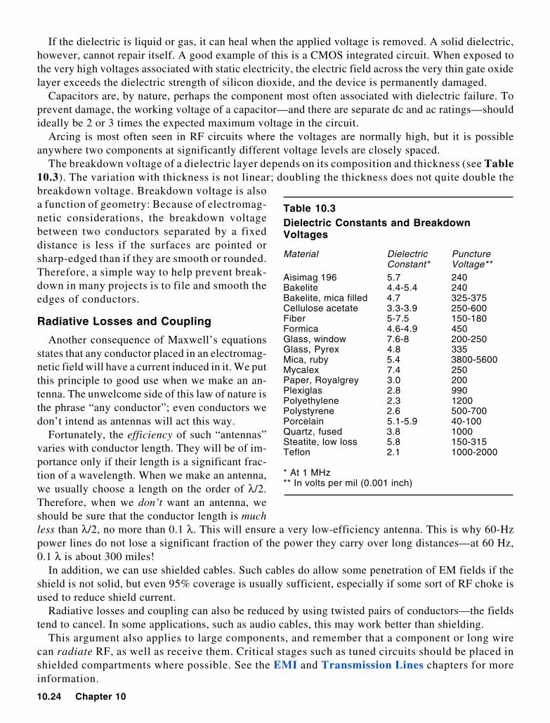
The breakdown voltage of a dielectric layer depends on its composition and thickness (see Table10.3). The variation with thickness is not linear; doubling the thickness does not quite double thebreakdown voltage. Breakdown voltage is alsoa function of geometry: Because of electromag-netic considerations, the breakdown voltagebetween two conductors separated by a fixeddistance is less if the surfaces are pointed orsharp-edged than if they are smooth or rounded.Therefore, a simple way to help prevent break-down in many projects is to file and smooth theedges of conductors.
Radiative Losses and Coupling
Another consequence of Maxwell’s equationsstates that any conductor placed in an electromag-netic field will have a current induced in it. We putthis principle to good use when we make an an-tenna. The unwelcome side of this law of nature isthe phrase “any conductor”; even conductors wedon’t intend as antennas will act this way.
Fortunately, the efficiency of such “antennas”varies with conductor length. They will be of im-portance only if their length is a significant frac-tion of a wavelength. When we make an antenna,we usually choose a length on the order of λ/2.Therefore, when we don’t want an antenna, weshould be sure that the conductor length is muchless than λ/2, no more than 0.1 λ. This will ensure a very low-efficiency antenna. This is why 60-Hzpower lines do not lose a significant fraction of the power they carry over long distances—at 60 Hz,0.1 λ is about 300 miles!
In addition, we can use shielded cables. Such cables do allow some penetration of EM fields if theshield is not solid, but even 95% coverage is usually sufficient, especially if some sort of RF choke isused to reduce shield current.
Radiative losses and coupling can also be reduced by using twisted pairs of conductors—the fieldstend to cancel. In some applications, such as audio cables, this may work better than shielding.
This argument also applies to large components, and remember that a component or long wirecan radiate RF, as well as receive them. Critical stages such as tuned circuits should be placed inshielded compartments where possible. See the EMI and Transmission Lines chapters for moreinformation.
Table 10.3Dielectric Constants and BreakdownVoltages
Material Dielectric PunctureConstant* Voltage**
Aisimag 196 5.7 240Bakelite 4.4-5.4 240Bakelite, mica filled 4.7 325-375Cellulose acetate 3.3-3.9 250-600Fiber 5-7.5 150-180Formica 4.6-4.9 450Glass, window 7.6-8 200-250Glass, Pyrex 4.8 335Mica, ruby 5.4 3800-5600Mycalex 7.4 250Paper, Royalgrey 3.0 200Plexiglas 2.8 990Polyethylene 2.3 1200Polystyrene 2.6 500-700Porcelain 5.1-5.9 40-100Quartz, fused 3.8 1000Steatite, low loss 5.8 150-315Teflon 2.1 1000-2000
* At 1 MHz** In volts per mil (0.001 inch)
Real-World Component Characteristics 10.25
REMEDIES FOR PARASITICS
The most common effect (always the most annoying) of parasitics is to influence the resonant fre-quency of a tuned circuit. This shift could cause an oscillator to fail, or more commonly, to cause a stablecircuit to oscillate. It can also de-grade filter performance (more onthis later) and basically causingany number of frequency-relatedproblems.
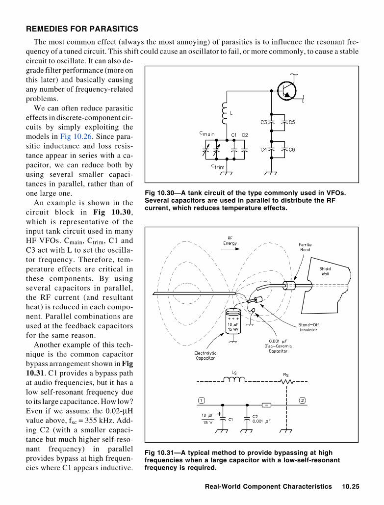
We can often reduce parasiticeffects in discrete-component cir-cuits by simply exploiting themodels in Fig 10.26. Since para-sitic inductance and loss resis-tance appear in series with a ca-pacitor, we can reduce both byusing several smaller capaci-tances in parallel, rather than ofone large one.
An example is shown in thecircuit block in Fig 10.30,which is representative of theinput tank circuit used in manyHF VFOs. Cmain, Ctrim, C1 andC3 act with L to set the oscilla-tor frequency. Therefore, tem-perature effects are critical inthese components. By usingseveral capacitors in parallel,the RF current (and resultantheat) is reduced in each compo-nent. Parallel combinations areused at the feedback capacitorsfor the same reason.
Another example of this tech-nique is the common capacitorbypass arrangement shown in Fig10.31. C1 provides a bypass pathat audio frequencies, but it has alow self-resonant frequency dueto its large capacitance. How low?Even if we assume the 0.02-µHvalue above, fsc = 355 kHz. Add-ing C2 (with a smaller capaci-tance but much higher self-reso-nant frequency) in parallelprovides bypass at high frequen-cies where C1 appears inductive.
Fig 10.30—A tank circuit of the type commonly used in VFOs.Several capacitors are used in parallel to distribute the RFcurrent, which reduces temperature effects.
Fig 10.31—A typical method to provide bypassing at highfrequencies when a large capacitor with a low-self-resonantfrequency is required.
10.26 Chapter 10
Construction Techniques
These concepts also help explain why so many different components exist with similar values. As anexample, assume you’re working on a project that requires you to wind a 5 µH inductor. Looking at thecoil inductance formula in the AC Theory chapter, it comes to mind that many combinations of lengthand diameter could yield the desired inductance. If you happen to have both 0.5 and 1-inch coil forms,why should you select one over the other? To eliminate some other variables, let’s make both coils 1 inchlong, close-wound, and give them 1-inch leads on each end.
Let’s calculate the number of turns required for each. On a 0.5-inch-diameter form:
( ) ( )[ ]
turns3.315.0
1405.0185n
=
×+×=
This means coil 1 will be made from #20 wire (29.9 turns per inch). Coil 2, on the 1-inch form, yields
( ) ( )[ ]
turns0.171
1401185n
=
×+×=
which requires #15 wire in order to be close-wound.What are the series resistances associated with each? For coil 1, the total wire length is 2 inches +
(31.3 × π × 0.5) = 51 inches, which at 10.1 Ω /1000 ft gives Rs = 0.043 Ω at dc. Coil 2 has a total wirelength of 2 inches + (17.0 × π × 1) = 55 inches, which at 3.18 Ω /1000 ft gives a dc resistance ofRs = 0.015 Ω, or about 1/3 that of coil 1. Furthermore, at RF, coil 1 will begin to suffer from skin effectat a frequency about 3 times lower than coil 2 because of its smaller conductor diameter. Therefore, ifQ were the sole consideration, it would be better to use the larger diameter coil.
Q is not the only concern, however. Such coils are often placed in shielded enclosures. Rule of thumbsays the enclosure should be at least one coil diameter from the coil on all sides. That is, 3×3×2 inchesfor the large coil and 1.5×1.5×1.5 for the small coil, a volume difference of over 500%.
Real-World Component Characteristics 10.27
Any real energized circuit consumes electric power because any real circuit contains components thatconvert electricity into other forms of energy.1 This dissipated power appears in many forms. Forexample, a loudspeaker converts electrical energy into the motion of air molecules we call sound. Anantenna (or a light bulb) converts electricity into electromagnetic radiation. Charging a battery convertselectrical energy into chemical energy (which is then converted back to electrical energy upon dis-charge). But the most common transformation by far is the conversion, through some form of resistance,of electricity into heat.
Sometimes the power lost to heat serves a useful purpose—toasters and hair dryers come to mind. Butmost of the time, this heat represents a power loss that is to be minimized wherever possible or at leasttaken into account. Since all real circuits contain resistance, even those circuits (such as a loudspeaker)whose primary purpose is to convert electricity to some other form of energy also convert some part oftheir input power to heat. Often, such losses are negligible, but sometimes they are not.
If unintended heat generation becomes significant, the involved components will get warm. Problemsarise when the temperature increase affects circuit operation by either• causing the component to fail, by explosion, melting, or other catastrophic event, or, more subtly,• causing a slight change in the properties of the component, such as through a temperature coefficient
(TC).In the first case, we can design conservatively, ensuring that components are rated to safely handle
two, three or more times the maximum power we expect them to dissipate. In the second case, we canspecify components with low TCs, or we can design the circuit to minimize the effect of any onecomponent. Occasionally we even exploit temperature effects (for example, using a resistor, capacitoror diode as a temperature sensor). Let’s look more closely at the two main categories of thermal effects.
HEAT DISSIPATION
Not surprisingly, heat dissipation (more correctly, the efficient removal of generated heat) becomesimportant in medium- to high-power circuits: power supplies, transmitting circuits and so on. Whilethese are not the only examples where elevated temperatures andrelated failures are of concern, the techniques we will discuss hereare applicable to all circuits.
Thermal Resistance
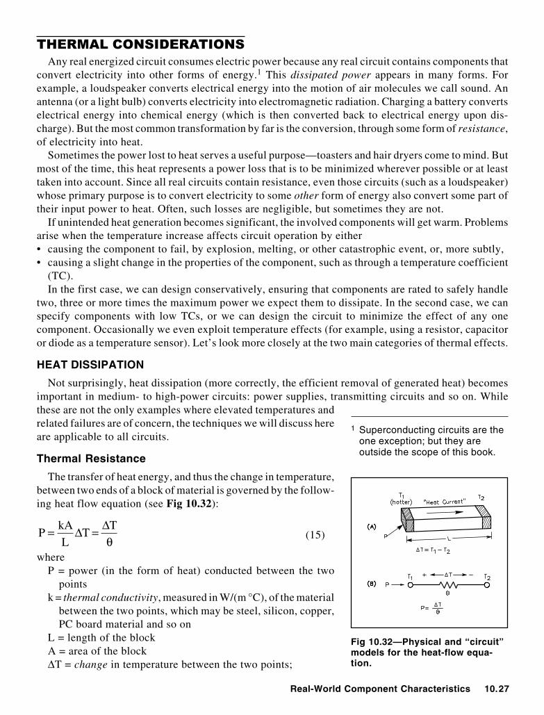
The transfer of heat energy, and thus the change in temperature,between two ends of a block of material is governed by the follow-ing heat flow equation (see Fig 10.32):
θ∆=∆= T
TL
kAP (15)
whereP = power (in the form of heat) conducted between the two
pointsk = thermal conductivity, measured in W/(m °C), of the material
between the two points, which may be steel, silicon, copper,PC board material and so on
L = length of the blockA = area of the block∆T = change in temperature between the two points;
Fig 10.32—Physical and “circuit”models for the heat-flow equa-tion.
1 Superconducting circuits are theone exception; but they areoutside the scope of this book.
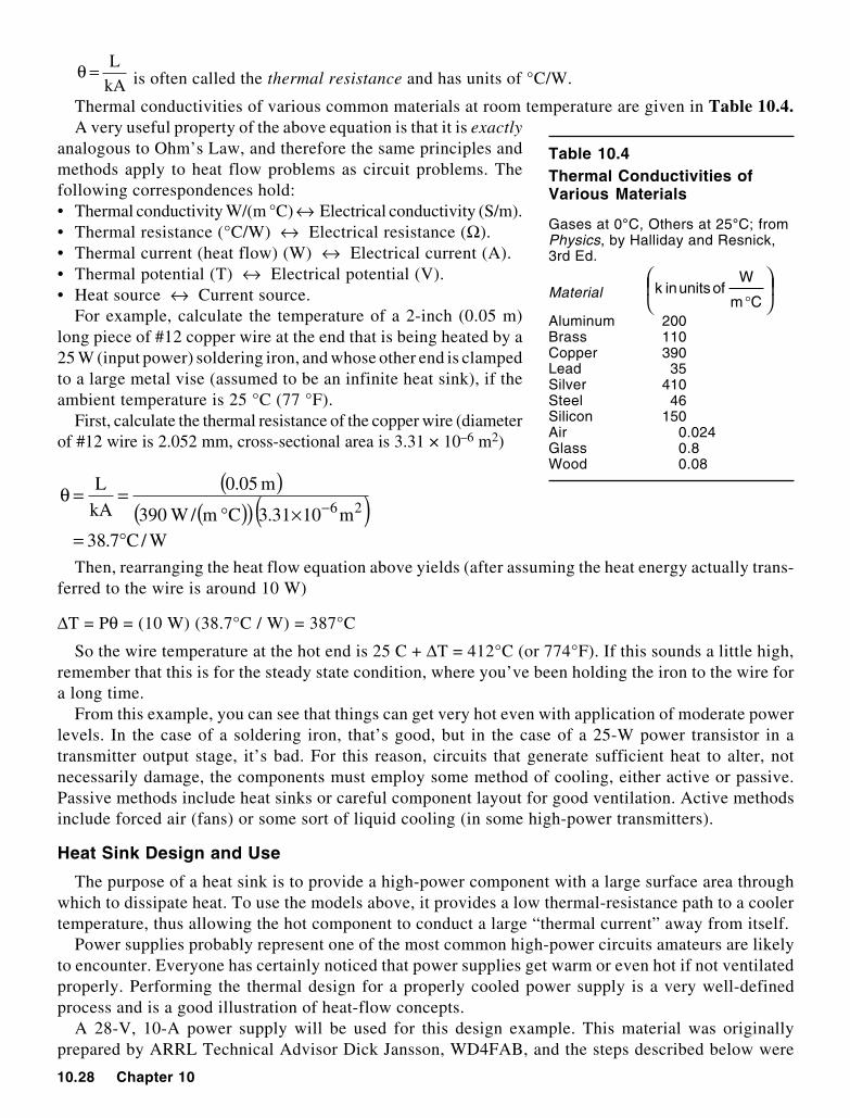
10.28 Chapter 10
kA
L=θ is often called the thermal resistance and has units of °C/W.
Thermal conductivities of various common materials at room temperature are given in Table 10.4.A very useful property of the above equation is that it is exactly
analogous to Ohm’s Law, and therefore the same principles andmethods apply to heat flow problems as circuit problems. Thefollowing correspondences hold:• Thermal conductivity W/(m °C) ↔ Electrical conductivity (S/m).• Thermal resistance (°C/W) ↔ Electrical resistance (Ω).• Thermal current (heat flow) (W) ↔ Electrical current (A).• Thermal potential (T) ↔ Electrical potential (V).• Heat source ↔ Current source.
For example, calculate the temperature of a 2-inch (0.05 m)long piece of #12 copper wire at the end that is being heated by a25 W (input power) soldering iron, and whose other end is clampedto a large metal vise (assumed to be an infinite heat sink), if theambient temperature is 25 °C (77 °F).
First, calculate the thermal resistance of the copper wire (diameterof #12 wire is 2.052 mm, cross-sectional area is 3.31 × 10⁻⁶ m2)
( )( )( )( )
W/C7.38m1031.3Cm/W390
m05.0
kA
L26
°=×°
==θ−
Then, rearranging the heat flow equation above yields (after assuming the heat energy actually trans-ferred to the wire is around 10 W)
∆T = Pθ = (10 W) (38.7°C / W) = 387°C
So the wire temperature at the hot end is 25 C + ∆T = 412°C (or 774°F). If this sounds a little high,remember that this is for the steady state condition, where you’ve been holding the iron to the wire fora long time.
From this example, you can see that things can get very hot even with application of moderate powerlevels. In the case of a soldering iron, that’s good, but in the case of a 25-W power transistor in atransmitter output stage, it’s bad. For this reason, circuits that generate sufficient heat to alter, notnecessarily damage, the components must employ some method of cooling, either active or passive.Passive methods include heat sinks or careful component layout for good ventilation. Active methodsinclude forced air (fans) or some sort of liquid cooling (in some high-power transmitters).
Heat Sink Design and Use
The purpose of a heat sink is to provide a high-power component with a large surface area throughwhich to dissipate heat. To use the models above, it provides a low thermal-resistance path to a coolertemperature, thus allowing the hot component to conduct a large “thermal current” away from itself.
Power supplies probably represent one of the most common high-power circuits amateurs are likelyto encounter. Everyone has certainly noticed that power supplies get warm or even hot if not ventilatedproperly. Performing the thermal design for a properly cooled power supply is a very well-definedprocess and is a good illustration of heat-flow concepts.
A 28-V, 10-A power supply will be used for this design example. This material was originallyprepared by ARRL Technical Advisor Dick Jansson, WD4FAB, and the steps described below were
Table 10.4Thermal Conductivities ofVarious Materials
Gases at 0°C, Others at 25°C; fromPhysics, by Halliday and Resnick,3rd Ed.
Material
°C m
W of units ink
Aluminum 200Brass 110Copper 390Lead 35Silver 410Steel 46Silicon 150Air 0.024Glass 0.8Wood 0.08
Real-World Component Characteristics 10.29
actually followed during the design of that supply.An outline of the design procedure shows the logic applied:
1. Determine the expected power dissipation (Pin).2. Identify the requirements for the dissipating elements (maximum component temperature).3. Estimate heat-sink requirements.4. Rework the electronic device (if necessary) to meet the thermal requirements.5. Select the heat exchanger (from heat sink data sheets).
The first step is to estimate the filtered, unregulated supply voltage under full load. Since the trans-former secondary output is 32 V ac (RMS) and feeds a full-wave bridge rectifier, let’s estimate 40 V asthe filtered dc output at a 10-A load.
The next step is to determine our critical components and estimate their power dissipations. In aregulated power supply, the pass transistors are responsible for nearly all the power lost to heat. Underfull load, and allowing for some small voltage drops in the power-transistor emitter circuitry, the outputof the series pass transistors is about 29 V for a delivered 28 V under a 10-A load. With an unregulatedinput voltage of 40 V, the total energy heat dissipated in the pass transistors is (40 V – 29 V) × 10 A =110 W. The heat sink for this power supply must be able to handle that amount of dissipation and stillkeep the transistor junctions below the specified safe operating temperature limits. It is a good rule ofthumb to select a transistor that has a maximum power dissipation of twice the desired output power.
Now, consider the ratings of the pass transistors to be used. This supply calls for 2N3055s as passtransistors. The data sheet shows that a 2N3055 is rated for 15-A service and 115-W dissipation. But thedesign uses four in parallel. Why? Here we must look past the big, bold type at the top of the data sheetto such subtle characteristics as the junction-to-case thermal resistance, θjc, and the maximum allowablejunction temperature, Tj.
The 2N3055 data sheet shows θjc = 1.52°C/W, and a maximum allowable case (and junction) tempera-ture of 220 °C. While it seems that one 2N3055 could barely, on paper at least, handle the electricalrequirements, at what temperature would it operate?
To answer that, we must model the entire “thermal circuit” of operation, starting with the transistorjunction on one end and ending at some point with the ambient air. A reasonable model is shown in Fig10.33. The ambient air is considered here as an infinite heat sink; that is, its temperature is assumed tobe a constant 25°C (77°F). θjc is the thermal resistance from the transistor junction to its case. θcs is theresistance of the mounting interface between the transistor case and the heat sink. θsa is the thermalresistance between the heat sink and the ambient air. In this “circuit,” the generation of heat (the “thermalcurrent source”) occurs in the transistor at Pin.
Proper mounting of most TO-3 package power transistors such as the 2N3055 requires that they havean electrical insulator between the transistor case and the heat sink. However, this electrical insulatormust at the same time exhibit a low thermal resistance. To achieve a quality mounting, use thin polyimidor mica formed washers and a suitable thermal compound to exclude air from the interstitial space.“Thermal greases” are commonly available for this function. Any silicone grease may be used, but filledsilicone oils made specifically for this purpose are better.
Using such techniques, aconservatively high value forθcs is 0.50°C/W. Lower valuesare possible, but the techniquesneeded to achieve them are ex-pensive and not generally avail-able to the average amateur.Furthermore, this value of θcs
is already much lower than θjc,Fig 10.33—Resistive model of thermal conduction in a powertransistor and associated heat sink. See text for calculations.
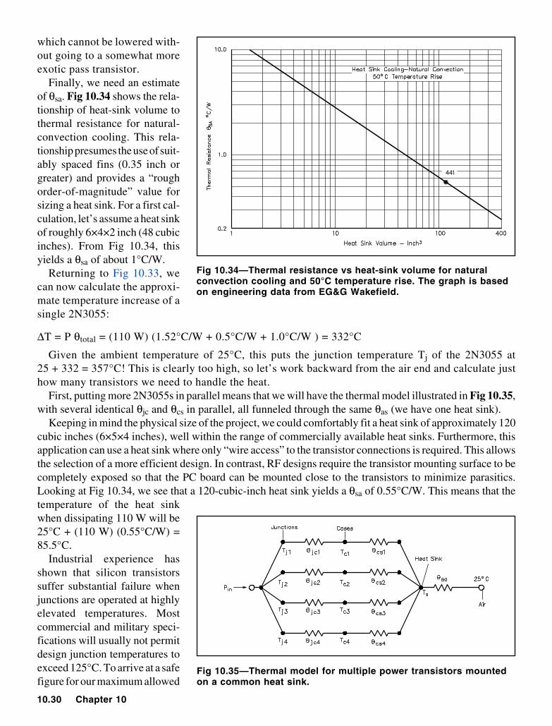
10.30 Chapter 10
which cannot be lowered with-out going to a somewhat moreexotic pass transistor.
Finally, we need an estimateof θsa. Fig 10.34 shows the rela-tionship of heat-sink volume tothermal resistance for natural-convection cooling. This rela-tionship presumes the use of suit-ably spaced fins (0.35 inch orgreater) and provides a “roughorder-of-magnitude” value forsizing a heat sink. For a first cal-culation, let’s assume a heat sinkof roughly 6×4×2 inch (48 cubicinches). From Fig 10.34, thisyields a θsa of about 1°C/W.
Returning to Fig 10.33, wecan now calculate the approxi-mate temperature increase of asingle 2N3055:
∆T = P θtotal = (110 W) (1.52°C/W + 0.5°C/W + 1.0°C/W ) = 332°C
Given the ambient temperature of 25°C, this puts the junction temperature Tj of the 2N3055 at25 + 332 = 357°C! This is clearly too high, so let’s work backward from the air end and calculate justhow many transistors we need to handle the heat.
First, putting more 2N3055s in parallel means that we will have the thermal model illustrated in Fig 10.35,with several identical θjc and θcs in parallel, all funneled through the same θas (we have one heat sink).
Keeping in mind the physical size of the project, we could comfortably fit a heat sink of approximately 120cubic inches (6×5×4 inches), well within the range of commercially available heat sinks. Furthermore, thisapplication can use a heat sink where only “wire access” to the transistor connections is required. This allowsthe selection of a more efficient design. In contrast, RF designs require the transistor mounting surface to becompletely exposed so that the PC board can be mounted close to the transistors to minimize parasitics.Looking at Fig 10.34, we see that a 120-cubic-inch heat sink yields a θsa of 0.55°C/W. This means that thetemperature of the heat sinkwhen dissipating 110 W will be25°C + (110 W) (0.55°C/W) =85.5°C.
Industrial experience hasshown that silicon transistorssuffer substantial failure whenjunctions are operated at highlyelevated temperatures. Mostcommercial and military speci-fications will usually not permitdesign junction temperatures toexceed 125°C. To arrive at a safefigure for our maximum allowed
Fig 10.34—Thermal resistance vs heat-sink volume for naturalconvection cooling and 50°C temperature rise. The graph is basedon engineering data from EG&G Wakefield.
Fig 10.35—Thermal model for multiple power transistors mountedon a common heat sink.
Real-World Component Characteristics 10.31
Tj, we must consider the intended use of the power supply. If we are using it in a 100% duty-cycle transmittingapplication such as RTTY or FM, the circuit will be dissipating 110 W continuously. For a lighter duty-cycleload such as CW or SSB, the “key-down” temperature can be slightly higher as long as the average is less than125°C. In this intermittent type of service, a good conservative figure to use is Tj = 150°C.
Given this scenario, the temperature rise across each transistor can be 150 – 85.5 = 64.5°C. Now,referencing Fig 10.35, remembering the total θ for each 2N3055 is 1.52 + 0.5 = 2.02°C/W, we cancalculate the maximum power each 2N3055 can safely dissipate:
W9.31W/C02.2
C5.64TP =
°°=
θ∆=
Thus, for 110 W full load, we need four 2N3055s to meet the thermal requirements of the design. Nowcomes the big question: What is the “right” heat sink to use? Wehave already established its requirements: it must be capable ofdissipating 110 W, and have a θsa of 0.55°C/W (see above).
A quick consultation with several manufacturer’s catalogs revealsthat Wakefield Engineering Co model nos. 441 and 435 heat sinksmeet the needs of this application.2 A Thermalloy model no. 6441 issuitable as well. Data published in the catalogs of these manufactur-ers show that in natural-convection service, the expected temperaturerise for 100 W dissipation would be just under 60°C, an almost per-fect fit for this application. Moreover, the no. 441 heat sink can easilymount four TO-3-style 2N3055 transistors. See Fig 10.36. Remem-ber: heat sinks should be mounted with the fins and transistor mount-ing area vertical to promote convection cooling.
The design procedure just described is applicable to any circuitwhere heat buildup is a potential problem. By using the thermal-resistance model, we can easily calculate whether or not an exter-nal means of cooling is necessary, and if so, how to choose it.Aside from heat sinks, forced air cooling (fans) is another com-mon method. In commercial transceivers, heat sinks with forced-air cooling are common.
Transistor Derating
Maximum ratings for power transistors are usually based on acase temperature of 25°C. These ratings will decrease with in-creasing operating temperature. Manufacturer’s data sheets usu-ally specify a derating fig-ure or curve that indicateshow the maximum ratingschange per degree rise intemperature. If such infor-mation is not available (oreven if it is!), it is a goodrule of thumb to select apower transistor with amaximum power dissipationof at least twice the desiredoutput power.
2 There are numerous manufac-turers of excellent heat sinks.References to any one manu-facturer are not intended toexclude the products of anyothers, nor to indicate anyparticular predisposition to onemanufacturer. The catalogs andproducts referred to here arefrom: EG&G Wakefield Engineer-ing (see the Address List in theReferences chapter).
Fig 10.36—An EG&G Wakefield441 heat sink with four 2N3055transistors mounted.
(A)(B)
10.32 Chapter 10
Rectifiers
Diodes are physically quite small, and they operate at high current densities. As a result their heat-handling capabilities are somewhat limited. Normally, this is not a problem in high-voltage, low-currentsupplies. The use of high-current (2 A or greater) rectifiers at or near their maximum ratings, however,requires some form of heat sinking. Frequently, mounting the rectifier on the main chassis (directly, or withthin mica insulating washers) will suffice. If the diode is insulated from the chassis, thin layers of siliconegrease should be used to ensure good heat conduction. Large, high-current rectifiers often require special heatsinks to maintain a safe operating temperature. Forced-air cooling is sometimes used as a further aid.
Forced-Air Cooling
In Amateur Radio today, forced-air cooling is most commonly found in vacuum-tube circuits or inpower supplies built in small enclosures, such as those in solid-state transceivers or computers. Fans orblowers are commonly specified in cubic feet per minute (CFM). While the nomenclature and specifi-cations differ from those used for heat sinks, the idea remains the same: to offer a low thermal resistancebetween the inside of the enclosure and the (ambient) exterior.
For forced air cooling, we basically use the “one resistor” thermal model of Fig 10.32. The importantquantity to be determined is heat generation, Pin. For a power supply, this can be easily estimated as thedifference between the input power, measured at the transformer primary, and the output power at full load.For variable-voltage supplies, the worst-case output condition is minimum voltage with maximum current.
A discussion of forced-air tube cooling appears in the RF Power Amplifiers chapter.
TEMPERATURE STABILITY
Aside from catastrophic failure, temperature changes may also adversely affect circuits if the TCs ofone or more components is too large. If the resultant change is not too critical, adequate temperaturestability can often be achieved simply by using higher-precision components with low TCs (such as NP0/C0G capacitors or metal-film resistors). For applications where this is impractical or impossible (suchas many solid-state circuits), we can minimize temperature sensitivity by compensation or matching—using temperature coefficients to our advantage.
Compensation is accomplished in one of two ways. If we wish to keep a certain circuit quantityconstant, we can interconnect pairs of components that have equal but opposite TCs. For example, aresistor with a negative TC can be placed in series with a positive TC resistor to keep thetotal resistance constant. Conversely, if the important point is to keep the difference between twoquantities constant, we can use components with the same TC so that the pair “tracks.” That is, they bothchange by the same amount with temperature.
An example of this is a Zener reference circuit. Since the I-V equation for a diode is strongly affected byoperating temperature, circuits that use diodes or transistors to generate stable reference voltages must usesome form of temperature compensation. Since, for a constant current, a reverse-biased PN junction has anegative voltage TC while a forward-biased junction has a positive voltage TC, a good way to temperature-compensate a Zener reference diode is to place one or more forward-biased diodes in series with it.
RF Heating
RF current often causes component heating problems where the same level of dc current may not. Anexample is the tank circuit of an RF oscillator. If several small capacitors are connected in parallel toachieve a desired capacitance, skin effect will be reduced and the total surface area available for heatdissipation will be increased, thus significantly reducing the RF heating effects as compared to a singlelarge capacitor. This technique can be applied to any similar situation; the general idea is to divide theheating among as many components as possible.
Real-World Component Characteristics 10.33
Hams today enjoy the easy availability of tremendous computing power to aid them in their hobby.A commercial application that computers perform very well is circuit simulation. Today anyone withaccess to a computer software bulletin board is likely to find shareware or other inexpensive softwareto perform such analysis. Indeed, ARRL offers ARRL Radio Designer, which provides excellent RFdesign capabilities at a reasonable price. Radio Designer is discussed in October 1994 QST and asubsequent QST column, “Exploring RF.”
The advantages of computer circuit simulation over pencil-and-paper calculation are many. Forexample, while the analysis of a small circuit, say 5 to 10 components, may be recomputed without toomuch effort if the design changes, the same is not true for a 50 to 100-component circuit. Indeed, thelarger circuit may require too many simplifying assumptions to calculate by hand at all. It is much fasterto watch and adjust the response of a circuit on a computer screen than to breadboard the circuit in searchof the same information.
All circuit simulators, including SPICE, work from a netlist that is simply a component-by-componentlist of the circuit that tells the program how components are interconnected. The program then usesstandard techniques of numerical analysis and matrix mathematics to calculate the analysis you wish toperform. Common analyses include dc and ac bias and operating point calculations, frequency responsecurves, transient analysis (looking at waveforms in the circuit over a specified period of time), Fouriertransforms, transfer functions, two-port parameter calculations, and pole-zero analysis. Many packagesalso perform sensitivity analyses: calculating what happens to the voltages and currents as you sweepthe value(s) of an individual component (or group of components), and statistical analyses: determiningte variational “window” of the system response that would result if all component values randomlyvaried by a given tolerance (also known as Monte Carlo analysis).
Beware!
Before we turn to a brief introduction to circuit simulation for the amateur, a caveat to the reader isdefinitely in order: However fast and powerful the computer may seem, keep in mind that it is onlyanother tool in your workshop, just like your ’scope or soldering iron. Circuit simulations are onlymeaningful if you can interpret the results correctly, and a good initial circuit design based on realexperience and common sense is mandatory. SPICE and other programs have no problem with a bench-top power supply delivering 10,000 V to a 5-Ω resistor because you made a mistake when specifyingthe circuit. Software also won’t remind you that the resistor better be rated for 20 megawatts! Remember,the real power behind any simulation software is your mind.
SPICE
The electronics industry has been the main consumer of circuit simulation packages ever since the devel-opment of SPICE (or Simulation Program with Integrated Circuit Emphasis) on mainframe systems in themid 1970s. While many companies today produce other simulation software, SPICE remains the de factoindustry standard. SPICE itself now exists in many “flavors” and specially tailored versions for desktopcomputers are sold by several companies, including PSPICE by Microsim Corp and HSPICE by Intusoft. Infact, an “evaluation” copy of PSPICE has been placed in the public domain by Microsim and is probably theeasiest and most inexpensive way for amateurs to begin circuit simulation. It may be obtained (with acompanion reference book) from technical bookstores, and also from many sites on the Internet. See Chapter30, References, for contact information for Microsim and Intusoft.
A Basic Circuit
Consider the simple RC low-pass filter in Fig 10.37A. To simulate this circuit, we must first precisely
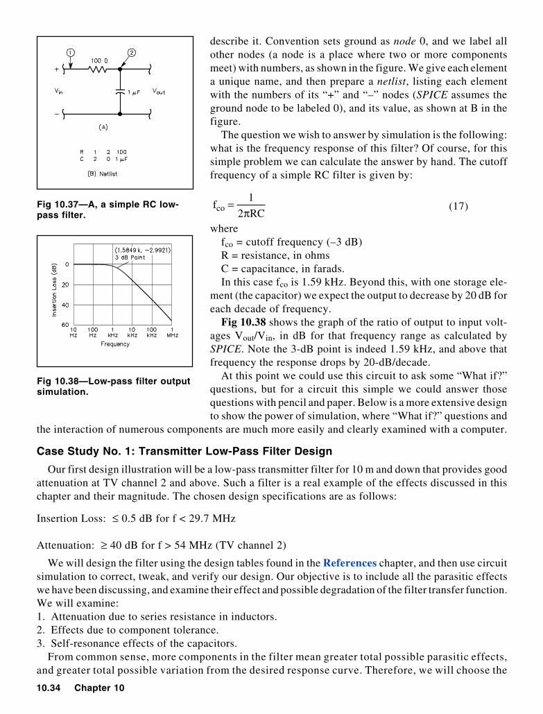
10.34 Chapter 10
describe it. Convention sets ground as node 0, and we label allother nodes (a node is a place where two or more componentsmeet) with numbers, as shown in the figure. We give each elementa unique name, and then prepare a netlist, listing each elementwith the numbers of its “+” and “–” nodes (SPICE assumes theground node to be labeled 0), and its value, as shown at B in thefigure.
The question we wish to answer by simulation is the following:what is the frequency response of this filter? Of course, for thissimple problem we can calculate the answer by hand. The cutofffrequency of a simple RC filter is given by:
RC2
1fco π
= (17)
wherefco = cutoff frequency (–3 dB)R = resistance, in ohmsC = capacitance, in farads.In this case fco is 1.59 kHz. Beyond this, with one storage ele-
ment (the capacitor) we expect the output to decrease by 20 dB foreach decade of frequency.
Fig 10.38 shows the graph of the ratio of output to input volt-ages Vout/Vin, in dB for that frequency range as calculated bySPICE. Note the 3-dB point is indeed 1.59 kHz, and above thatfrequency the response drops by 20-dB/decade.
At this point we could use this circuit to ask some “What if?”questions, but for a circuit this simple we could answer thosequestions with pencil and paper. Below is a more extensive designto show the power of simulation, where “What if?” questions and
the interaction of numerous components are much more easily and clearly examined with a computer.
Case Study No. 1: Transmitter Low-Pass Filter Design
Our first design illustration will be a low-pass transmitter filter for 10 m and down that provides goodattenuation at TV channel 2 and above. Such a filter is a real example of the effects discussed in thischapter and their magnitude. The chosen design specifications are as follows:
Insertion Loss: ≤ 0.5 dB for f < 29.7 MHz
Attenuation: ≥ 40 dB for f > 54 MHz (TV channel 2)
We will design the filter using the design tables found in the References chapter, and then use circuitsimulation to correct, tweak, and verify our design. Our objective is to include all the parasitic effectswe have been discussing, and examine their effect and possible degradation of the filter transfer function.We will examine:1. Attenuation due to series resistance in inductors.2. Effects due to component tolerance.3. Self-resonance effects of the capacitors.
From common sense, more components in the filter mean greater total possible parasitic effects,and greater total possible variation from the desired response curve. Therefore, we will choose the
Fig 10.38—Low-pass filter outputsimulation.
Fig 10.37—A, a simple RC low-pass filter.
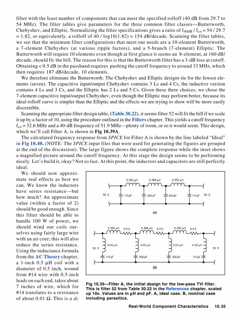
Real-World Component Characteristics 10.35
filter with the least number of components that can meet the specified rolloff (40 dB from 29.7 to54 MHz). The filter tables give parameters for the three common filter classes—Butterworth,Chebyshev, and Elliptic. Normalizing the filter specifications gives a ratio of f40dB / fco = 54 / 29.7= 1.82, or equivalently, a rolloff of 40 / log10(1.82) = 154 dB/decade. Scanning the filter tables,we see that the minimum filter configurations that meet our needs are a 10-element Butterworth,a 7-element Chebyshev (at various ripple factors), and a 5-branch (7-element) Elliptic. TheButterworth will require 10 elements even though at first glance it seems an 8-element, at 160 dB/decade, should fit the bill. The reason for this is that the Butterworth filter has a 3-dB loss at cutoff.Obtaining < 0.5 dB in the passband requires pushing the cutoff frequency to around 33 MHz, whichthen requires 187 dB/decade, 10 elements.
We therefore eliminate the Butterworth. The Chebyshev and Elliptic designs tie for the fewest ele-ments (seven). The capacitive input/output Chebyshev contains 3 Ls and 4 Cs, the inductive versioncontains 4 Ls and 3 Cs, and the Elliptic has 2 Ls and 5 Cs. Given these three choices, we chose the7-element capacitive input/output Chebyshev, even though the Elliptic may perform better, because itsideal rolloff curve is simpler than the Elliptic and the effects we are trying to show will be more easilydiscernible.
Scanning the appropriate filter design table, (Table 30.22), it seems filter 52 will fit the bill if we scaleit up by a factor of 10, using the procedure outlined in the Filters chapter. This yields a cutoff frequencyfco = 32.6 MHz and a 40-dB frequency of 51.9 MHz—plenty of room, or so it would seem. This design,which we’ll call Filter A, is shown in Fig 10.39A.
The calculated frequency response from SPICE for Filter A is shown by the line labeled “Ideal”in Fig 10.40. (NOTE: The SPICE input files that were used for generating the figures are groupedat the end of the discussion). The large figure shows the complete response while the inset showsa magnified picture around the cutoff frequency. At this stage the design seems to be performingnicely. Let’s build it, okay? Not so fast. At this point, the inductors and capacitors are still perfectlyideal.
We should now approxi-mate real effects as best wecan. We know the inductorshave series resistance—buthow much? An approximatevalue (within a factor of 2)should be good enough. Sincethis filter should be able tohandle 100 W of power, weshould wind our coils our-selves using fairly large wirewith an air core; this will alsoreduce the series resistance.Using the inductance formulafrom the AC Theory chapter,a 1-inch 0.5 µH coil with adiameter of 0.5 inch, woundfrom #14 wire with 0.5-inchleads on each end, takes about7 inches of wire, which for#14 translates to a resistanceof about 0.01 Ω. This is a dc
Fig 10.39—Filter A, the initial design for the low-pass TVI filter.This is filter 52 from Table 30.22 in the References chapter, scaledup 10×××××. Values are in µµµµµH and pF. A, ideal case. B, nominal caseincluding parasitics.
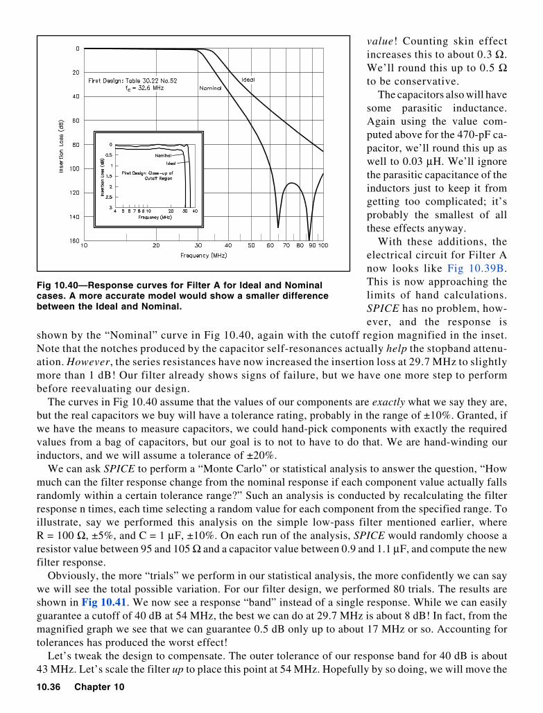
10.36 Chapter 10
value! Counting skin effectincreases this to about 0.3 Ω.We’ll round this up to 0.5 Ωto be conservative.
The capacitors also will havesome parasitic inductance.Again using the value com-puted above for the 470-pF ca-pacitor, we’ll round this up aswell to 0.03 µH. We’ll ignorethe parasitic capacitance of theinductors just to keep it fromgetting too complicated; it’sprobably the smallest of allthese effects anyway.
With these additions, theelectrical circuit for Filter Anow looks like Fig 10.39B.This is now approaching thelimits of hand calculations.SPICE has no problem, how-ever, and the response is
shown by the “Nominal” curve in Fig 10.40, again with the cutoff region magnified in the inset.Note that the notches produced by the capacitor self-resonances actually help the stopband attenu-ation. However, the series resistances have now increased the insertion loss at 29.7 MHz to slightlymore than 1 dB! Our filter already shows signs of failure, but we have one more step to performbefore reevaluating our design.
The curves in Fig 10.40 assume that the values of our components are exactly what we say they are,but the real capacitors we buy will have a tolerance rating, probably in the range of ±10%. Granted, ifwe have the means to measure capacitors, we could hand-pick components with exactly the requiredvalues from a bag of capacitors, but our goal is to not to have to do that. We are hand-winding ourinductors, and we will assume a tolerance of ±20%.
We can ask SPICE to perform a “Monte Carlo” or statistical analysis to answer the question, “Howmuch can the filter response change from the nominal response if each component value actually fallsrandomly within a certain tolerance range?” Such an analysis is conducted by recalculating the filterresponse n times, each time selecting a random value for each component from the specified range. Toillustrate, say we performed this analysis on the simple low-pass filter mentioned earlier, whereR = 100 Ω, ±5%, and C = 1 µF, ±10%. On each run of the analysis, SPICE would randomly choose aresistor value between 95 and 105 Ω and a capacitor value between 0.9 and 1.1 µF, and compute the newfilter response.
Obviously, the more “trials” we perform in our statistical analysis, the more confidently we can saywe will see the total possible variation. For our filter design, we performed 80 trials. The results areshown in Fig 10.41. We now see a response “band” instead of a single response. While we can easilyguarantee a cutoff of 40 dB at 54 MHz, the best we can do at 29.7 MHz is about 8 dB! In fact, from themagnified graph we see that we can guarantee 0.5 dB only up to about 17 MHz or so. Accounting fortolerances has produced the worst effect!
Let’s tweak the design to compensate. The outer tolerance of our response band for 40 dB is about43 MHz. Let’s scale the filter up to place this point at 54 MHz. Hopefully by so doing, we will move the
Fig 10.40—Response curves for Filter A for Ideal and Nominalcases. A more accurate model would show a smaller differencebetween the Ideal and Nominal.
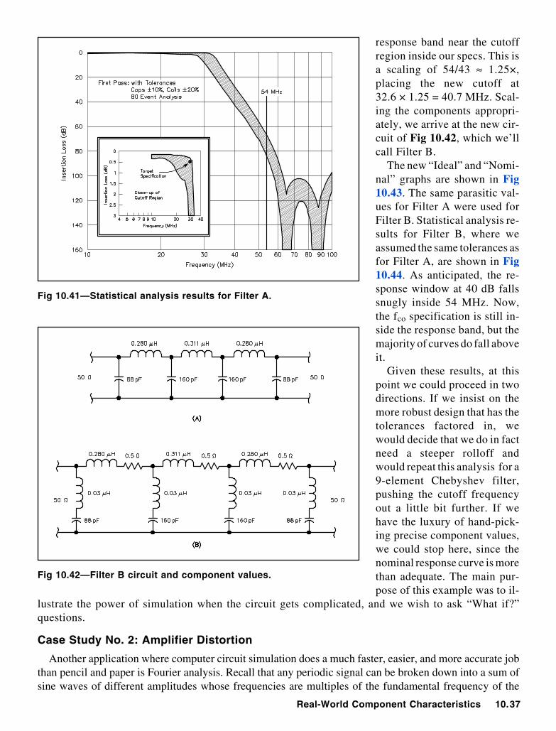
Real-World Component Characteristics 10.37
Fig 10.41—Statistical analysis results for Filter A.
Fig 10.42—Filter B circuit and component values.
response band near the cutoffregion inside our specs. This isa scaling of 54/43 ≈ 1.25×,placing the new cutoff at32.6 × 1.25 = 40.7 MHz. Scal-ing the components appropri-ately, we arrive at the new cir-cuit of Fig 10.42, which we’llcall Filter B.
The new “Ideal” and “Nomi-nal” graphs are shown in Fig10.43. The same parasitic val-ues for Filter A were used forFilter B. Statistical analysis re-sults for Filter B, where weassumed the same tolerances asfor Filter A, are shown in Fig10.44. As anticipated, the re-sponse window at 40 dB fallssnugly inside 54 MHz. Now,the fco specification is still in-side the response band, but themajority of curves do fall aboveit.
Given these results, at thispoint we could proceed in twodirections. If we insist on themore robust design that has thetolerances factored in, wewould decide that we do in factneed a steeper rolloff andwould repeat this analysis for a9-element Chebyshev filter,pushing the cutoff frequencyout a little bit further. If wehave the luxury of hand-pick-ing precise component values,we could stop here, since thenominal response curve is morethan adequate. The main pur-pose of this example was to il-
lustrate the power of simulation when the circuit gets complicated, and we wish to ask “What if?”questions.
Case Study No. 2: Amplifier Distortion
Another application where computer circuit simulation does a much faster, easier, and more accurate jobthan pencil and paper is Fourier analysis. Recall that any periodic signal can be broken down into a sum ofsine waves of different amplitudes whose frequencies are multiples of the fundamental frequency of the
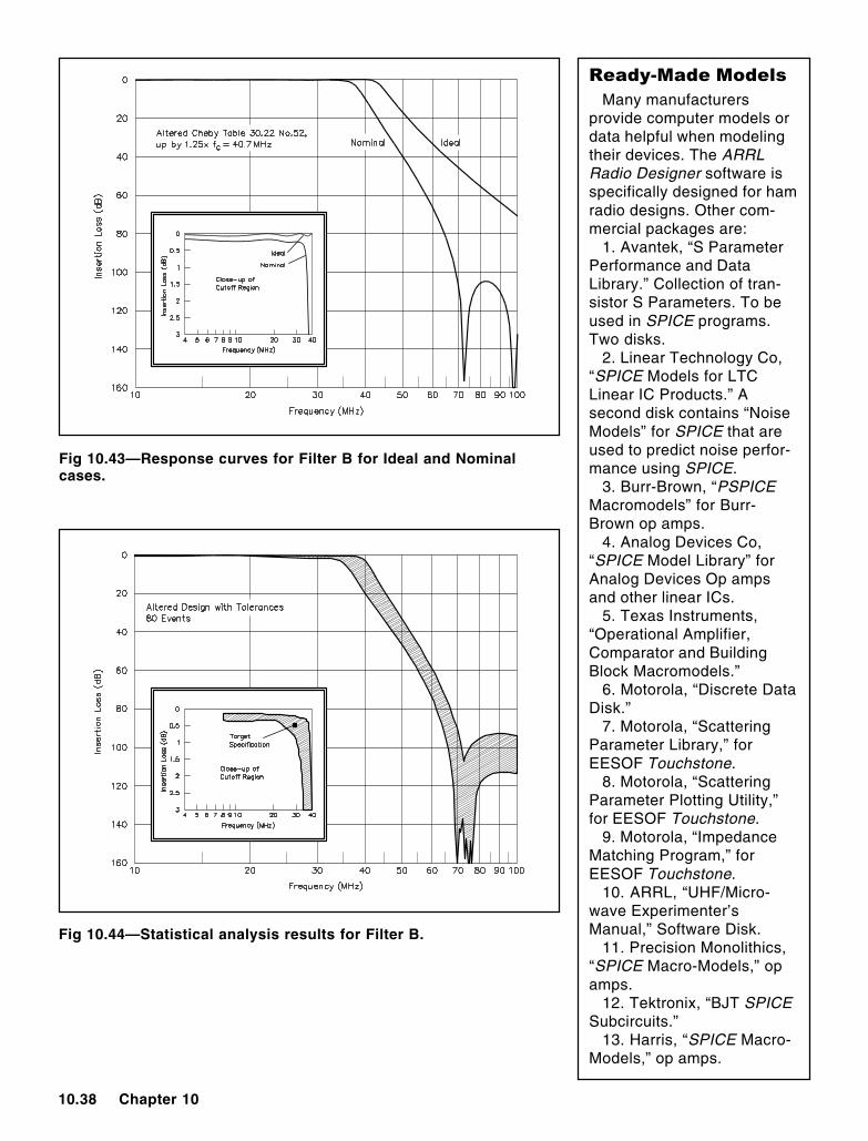
10.38 Chapter 10
Fig 10.44—Statistical analysis results for Filter B.
Fig 10.43—Response curves for Filter B for Ideal and Nominalcases.
Many manufacturersprovide computer models ordata helpful when modelingtheir devices. The ARRLRadio Designer software isspecifically designed for hamradio designs. Other com-mercial packages are:
1. Avantek, “S ParameterPerformance and DataLibrary.” Collection of tran-sistor S Parameters. To beused in SPICE programs.Two disks.
2. Linear Technology Co,“SPICE Models for LTCLinear IC Products.” Asecond disk contains “NoiseModels” for SPICE that areused to predict noise perfor-mance using SPICE.
3. Burr-Brown, “PSPICEMacromodels” for Burr-Brown op amps.
4. Analog Devices Co,“SPICE Model Library” forAnalog Devices Op ampsand other linear ICs.
5. Texas Instruments,“Operational Amplifier,Comparator and BuildingBlock Macromodels.”
6. Motorola, “Discrete DataDisk.”
7. Motorola, “ScatteringParameter Library,” forEESOF Touchstone.
8. Motorola, “ScatteringParameter Plotting Utility,”for EESOF Touchstone.
9. Motorola, “ImpedanceMatching Program,” forEESOF Touchstone.
10. ARRL, “UHF/Micro-wave Experimenter’sManual,” Software Disk.
11. Precision Monolithics,“SPICE Macro-Models,” opamps.
12. Tektronix, “BJT SPICESubcircuits.”
13. Harris, “SPICE Macro-Models,” op amps.
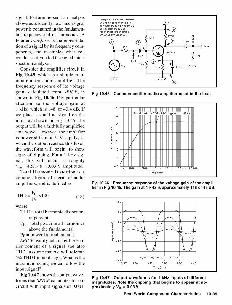
Real-World Component Characteristics 10.39
signal. Performing such an analysisallows us to identify how much signalpower is contained in the fundamen-tal frequency and its harmonics. AFourier transform is the representa-tion of a signal by its frequency com-ponents, and resembles what youwould see if you fed the signal into aspectrum analyzer.
Consider the amplifier circuit inFig 10.45, which is a simple com-mon-emitter audio amplifier. Thefrequency response of its voltagegain, calculated from SPICE, isshown in Fig 10.46. Pay particularattention to the voltage gain at1 kHz, which is 148, or 43.4 dB. Ifwe place a small ac signal on theinput as shown in Fig 10.45, theoutput will be a faithfully amplifiedsine wave. However, the amplifieris powered from a 9-V supply, sowhen the output reaches this level,the waveform will begin to showsigns of clipping. For a 1-kHz sig-nal, this will occur at roughlyVin = 4.5/148 = 0.03 V amplitude.
Total Harmonic Distortion is acommon figure of merit for audioamplifiers, and is defined as
100P
PTHD
F
H ×= (18)
whereTHD = total harmonic distortion,
in percentPH = total power in all harmonics
above the fundamentalPF = power in fundamental.SPICE readily calculates the Fou-
rier content of a signal and alsoTHD. Assume that we will tolerate5% THD for our design. What is themaximum swing we can allow theinput signal?
Fig 10.47 shows the output wave-forms that SPICE calculates for ourcircuit with input signals of 0.001,
Fig 10.45—Common-emitter audio amplifier used in the text.
Fig 10.46—Frequency response of the voltage gain of the ampli-fier in Fig 10.45. The gain at 1 kHz is approximately 148 or 43 dB.
Fig 10.47—Output waveforms for 1-kHz inputs of differentmagnitudes. Note the clipping that begins to appear at ap-proximately Vin = 0.03 V.
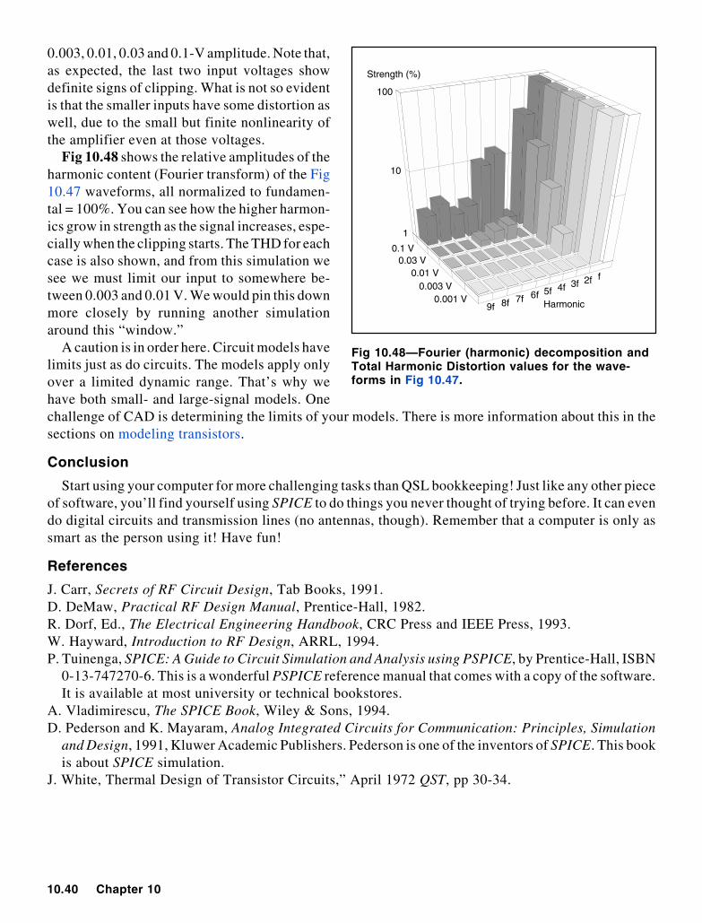
10.40 Chapter 10
0.003, 0.01, 0.03 and 0.1-V amplitude. Note that,as expected, the last two input voltages showdefinite signs of clipping. What is not so evidentis that the smaller inputs have some distortion aswell, due to the small but finite nonlinearity ofthe amplifier even at those voltages.
Fig 10.48 shows the relative amplitudes of theharmonic content (Fourier transform) of the Fig10.47 waveforms, all normalized to fundamen-tal = 100%. You can see how the higher harmon-ics grow in strength as the signal increases, espe-cially when the clipping starts. The THD for eachcase is also shown, and from this simulation wesee we must limit our input to somewhere be-tween 0.003 and 0.01 V. We would pin this downmore closely by running another simulationaround this “window.”
A caution is in order here. Circuit models havelimits just as do circuits. The models apply onlyover a limited dynamic range. That’s why wehave both small- and large-signal models. Onechallenge of CAD is determining the limits of your models. There is more information about this in thesections on modeling transistors.
Conclusion
Start using your computer for more challenging tasks than QSL bookkeeping! Just like any other pieceof software, you’ll find yourself using SPICE to do things you never thought of trying before. It can evendo digital circuits and transmission lines (no antennas, though). Remember that a computer is only assmart as the person using it! Have fun!
References
J. Carr, Secrets of RF Circuit Design, Tab Books, 1991.D. DeMaw, Practical RF Design Manual, Prentice-Hall, 1982.R. Dorf, Ed., The Electrical Engineering Handbook, CRC Press and IEEE Press, 1993.W. Hayward, Introduction to RF Design, ARRL, 1994.P. Tuinenga, SPICE: A Guide to Circuit Simulation and Analysis using PSPICE, by Prentice-Hall, ISBN
0-13-747270-6. This is a wonderful PSPICE reference manual that comes with a copy of the software.It is available at most university or technical bookstores.
A. Vladimirescu, The SPICE Book, Wiley & Sons, 1994.D. Pederson and K. Mayaram, Analog Integrated Circuits for Communication: Principles, Simulation
and Design, 1991, Kluwer Academic Publishers. Pederson is one of the inventors of SPICE. This bookis about SPICE simulation.
J. White, Thermal Design of Transistor Circuits,” April 1972 QST, pp 30-34.
Fig 10.48—Fourier (harmonic) decomposition andTotal Harmonic Distortion values for the wave-forms in Fig 10.47.
9f 8f 7f 6f5f 4f 3f 2f f
1
10
100
0.1 V0.03 V
0.01 V0.003 V
0.001 V Harmonic
Strength (%)
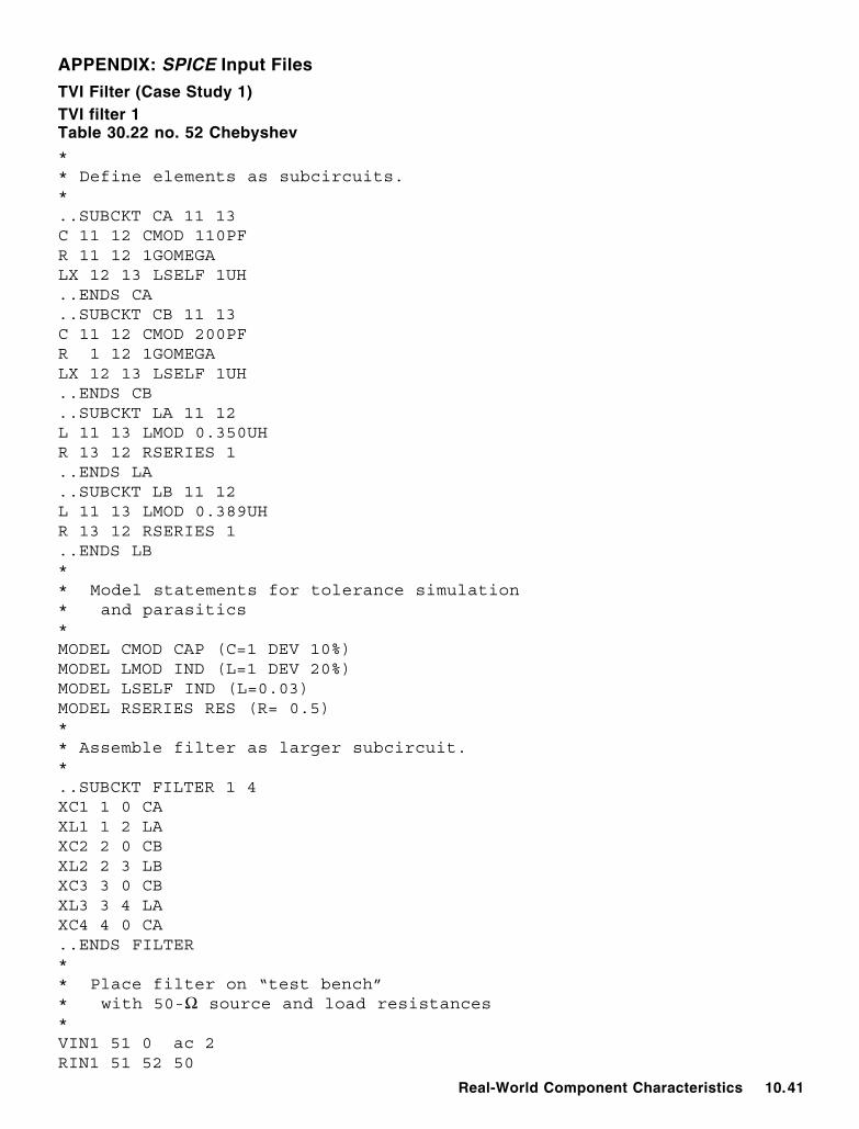
Real-World Component Characteristics 10.41
APPENDIX: SPICE Input Files
TVI Filter (Case Study 1)TVI filter 1Table 30.22 no. 52 Chebyshev** Define elements as subcircuits.*..SUBCKT CA 11 13C 11 12 CMOD 110PFR 11 12 1GOMEGALX 12 13 LSELF 1UH..ENDS CA..SUBCKT CB 11 13C 11 12 CMOD 200PFR 1 12 1GOMEGALX 12 13 LSELF 1UH..ENDS CB..SUBCKT LA 11 12L 11 13 LMOD 0.350UHR 13 12 RSERIES 1..ENDS LA..SUBCKT LB 11 12L 11 13 LMOD 0.389UHR 13 12 RSERIES 1..ENDS LB** Model statements for tolerance simulation* and parasitics*MODEL CMOD CAP (C=1 DEV 10%)MODEL LMOD IND (L=1 DEV 20%)MODEL LSELF IND (L=0.03)MODEL RSERIES RES (R= 0.5)** Assemble filter as larger subcircuit.*..SUBCKT FILTER 1 4XC1 1 0 CAXL1 1 2 LAXC2 2 0 CBXL2 2 3 LBXC3 3 0 CBXL3 3 4 LAXC4 4 0 CA..ENDS FILTER** Place filter on “test bench”* with 50-Ω source and load resistances*VIN1 51 0 ac 2RIN1 51 52 50
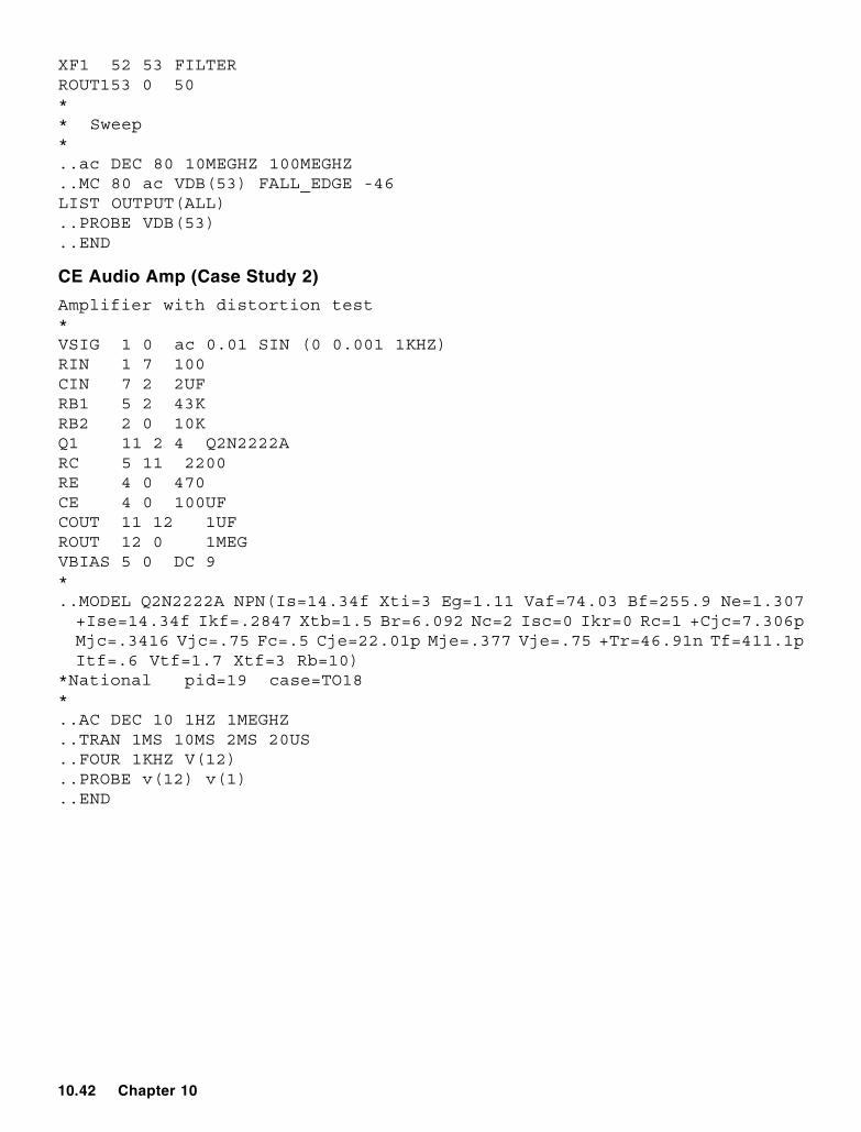
10.42 Chapter 10
XF1 52 53 FILTERROUT153 0 50** Sweep*..ac DEC 80 10MEGHZ 100MEGHZ..MC 80 ac VDB(53) FALL_EDGE -46LIST OUTPUT(ALL)..PROBE VDB(53)..END
CE Audio Amp (Case Study 2)
Amplifier with distortion test*VSIG 1 0 ac 0.01 SIN (0 0.001 1KHZ)RIN 1 7 100CIN 7 2 2UFRB1 5 2 43KRB2 2 0 10KQ1 11 2 4 Q2N2222ARC 5 11 2200RE 4 0 470CE 4 0 100UFCOUT 11 12 1UFROUT 12 0 1MEGVBIAS 5 0 DC 9*..MODEL Q2N2222A NPN(Is=14.34f Xti=3 Eg=1.11 Vaf=74.03 Bf=255.9 Ne=1.307+Ise=14.34f Ikf=.2847 Xtb=1.5 Br=6.092 Nc=2 Isc=0 Ikr=0 Rc=1 +Cjc=7.306pMjc=.3416 Vjc=.75 Fc=.5 Cje=22.01p Mje=.377 Vje=.75 +Tr=46.91n Tf=411.1pItf=.6 Vtf=1.7 Xtf=3 Rb=10)
*National pid=19 case=TO18*..AC DEC 10 1HZ 1MEGHZ..TRAN 1MS 10MS 2MS 20US..FOUR 1KHZ V(12)..PROBE v(12) v(1)..END
Real-World Component Characteristics 10.43
THE FUNDAMENTAL EQUATIONS
Design models are based on the physics of the components we use. The complexity of modelscan vary widely though, and many times we can use very simple models to achieve our goals.Increasingly complex models are developed and used only when demanded by the circuit applica-tion.
In this discussion, we will focus on simple models for bipolar transistors (BJTs) and FETs. Thesemodels are reasonably accurate at low frequencies, and they are of some use at RF. For more sophisti-cated RF models, look to professional RF-design literature. This discussion is adapted from WesHayward’s Introduction to RF Design. Derivations of the material shown here appear in that book, anexcellent text for the beginning RF designer.
This discussion is centered on NPN BJTs and N-channel JFETs. The material here applies to PNPsand P-channel FETs when you simply change the bias polarities.
First, consider the bipolar transistor as a current controlled device. When the base current controls thecollector current, this equation defines the transistor operation
Ic = βIb (19)
where β = common-emitter current gain.When we consider a transistor as a voltage-controlled device, this equation describes it (emitter
current, Ie, in terms of base-emitter voltage, Vbe):
Ie = Ies [exp(qV/kT) – 1]
≈ Ies exp(qV/kT) (20)
whereV = Vbe
q = electronic chargek = Boltzmann’s constantT = temperature in kelvins (K)Ib = emitter saturation current, typically 1 × 10–13 A.Both equations approximate models of more complex behavior. Equation 20 is a simplification of the
first Ebers-Moll model (Ref 1). More sophisticated models for BJTs are described by Getreu in Ref 2.Equations 19 and 20 apply to both transistor dc biasing and signal design.
The operation of an N-channel JFET can be characterized by
ID = IDSS (1 – Vsg/Vp)2 (21)
whereIDSS = drain saturation currentVsg = the source-gate voltageVp = the pinch-off voltage.This equation applies only so long as Vsg is between 0 and Vp. JFETs are seldom used with the gate-
to-channel diode forward biased. Drain current, ID, is 0 when Vsg exceeds Vp. This equation applies toboth biasing and signal design.
Now that we have some basic equations, let’s go on to some other areas:• Small-signal amplifier design (and application limits).• Large-signal amplifier design (distortion from nonlinearity).
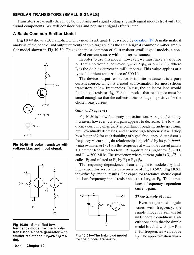
10.44 Chapter 10
BIPOLAR TRANSISTORS (SMALL SIGNALS)
Transistors are usually driven by both biasing and signal voltages. Small-signal models treat only thesignal components. We will consider bias and nonlinear signal effects later.
A Basic Common-Emitter Model
Fig 10.49 shows a BJT amplifier. The circuit is adequately described by equation 19. A mathematicalanalysis of the control and output currents and voltages yields the small-signal common-emitter ampli-fier model shown in Fig 10.50. This is the most common of all transistor small-signal models, a con-
trolled current source with emitter resistance.In order to use this model, however, we must have a value for
re. That’s no trouble, however, re = kT / qI0, or re = 26 / Ie, whereIe is the dc bias current in milliamperes. This value applies at atypical ambient temperature of 300 K.
The device output resistance is infinite because it is a purecurrent source, which is a good approximation for most silicontransistors at low frequencies. In use, the collector lead wouldfeed a load resistor, RL. For this model, that resistance must besmall enough so that the collector bias voltage is positive for thechosen bias current.
Gain vs Frequency
Fig 10.50 is a low frequency approximation. As signal frequencyincreases, however, current gain appears to decrease. The low-fre-quency current gain is β0. β0 is constant through the audio spectrum,but it eventually decreases, and at some high frequency it will dropby a factor of 2 for each doubling of signal frequency. A transistor’sfrequency vs current gain relationship is specified by its gain-band-width product, or FT. FT is the frequency at which the current gain is1. Common transistors for lower RF applications might have β0 = 100and FT = 500 MHz. The frequency where current gain is β0 2 iscalled Fβ and related to FT by Fβ = FT / β0.
The frequency dependence of current gain is modeled by add-ing a capacitor across the base resistor of Fig 10.50A; Fig 10.51,the hybrid-pi model results. The capacitor reactance should equalthe low-frequency input resistance, (β + 1)re, at Fβ. This simu-
lates a frequency-dependentcurrent gain.
Three Simple Models
Even though transistor gainvaries with frequency, thesimple model is still usefulunder certain conditions. Cal-culations show that the simplemodel is valid, with β = FT /F, for frequencies well aboveFβ. The approximation wors-
Fig 10.50—Simplified low-frequency model for the bipolartransistor, a “beta generator withemitter resistance.” re=26 / le(mAdc).
Fig 10.49—Bipolar transistor withvoltage bias and input signal.
Fig 10.51—The hybrid-pi modelfor the bipolar transistor.
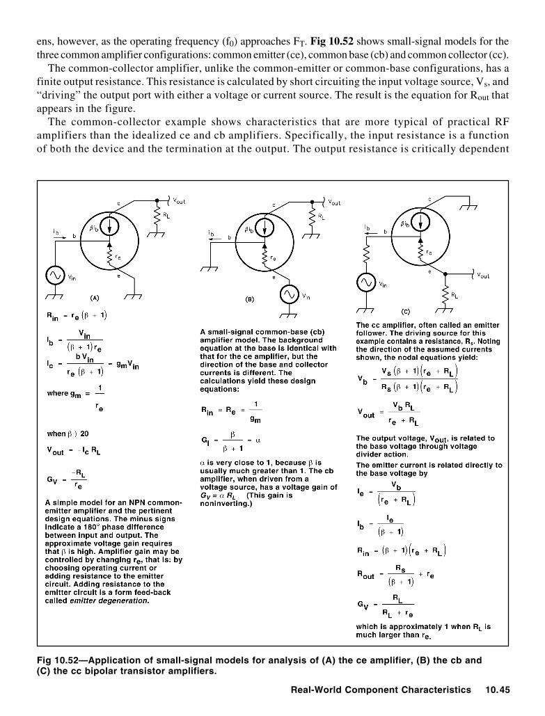
Real-World Component Characteristics 10.45
ens, however, as the operating frequency (f0) approaches FT. Fig 10.52 shows small-signal models for thethree common amplifier configurations: common emitter (ce), common base (cb) and common collector (cc).
The common-collector amplifier, unlike the common-emitter or common-base configurations, has afinite output resistance. This resistance is calculated by short circuiting the input voltage source, Vs, and“driving” the output port with either a voltage or current source. The result is the equation for Rout thatappears in the figure.
The common-collector example shows characteristics that are more typical of practical RFamplifiers than the idealized ce and cb amplifiers. Specifically, the input resistance is a functionof both the device and the termination at the output. The output resistance is critically dependent
Fig 10.52—Application of small-signal models for analysis of (A) the ce amplifier, (B) the cb and(C) the cc bipolar transistor amplifiers.
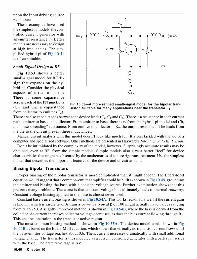
10.46 Chapter 10
upon the input driving sourceresistance.
These examples have usedthe simplest of models, the con-trolled current generator withan emitter resistance, re. Bettermodels are necessary to designat high frequencies. The sim-plified hybrid-pi of Fig 10.51is often suitable.
Small-Signal Design at RF
Fig 10.53 shows a bettersmall-signal model for RF de-sign that expands on the hy-brid-pi. Consider the physicalaspects of a real transistor:There is some capacitanceacross each of the PN junctions(Ccb and Cπ) a capacitancefrom collector to emitter (Cc).There are also capacitances between the device leads (Ce, Cb and Cc). There is a resistance in each currentpath, emitter to base and collector. From emitter to base, there is rπ from the hybrid-pi model and r´b,the “base spreading” resistance. From emitter to collector is Ro, the output resistance. The leads fromthe die to the circuit present three inductances.
Manual circuit analysis with this model doesn’t look like much fun. It’s best tackled with the aid of acomputer and specialized software. Other methods are presented in Hayward’s Introduction to RF Design.
Don’t be intimidated by the complexity of the model, however. Surprisingly accurate results may beobtained, even at RF, from the simple models. Simple models also give a better “feel” for devicecharacteristics that might be obscured by the mathematics of a more rigorous treatment. Use the simplestmodel that describes the important features of the device and circuit at hand.
Biasing Bipolar Transistors
Proper biasing of the bipolar transistor is more complicated than it might appear. The Ebers-Mollequation would suggest that a common-emitter amplifier could be built as shown in Fig 10.49, groundingthe emitter and biasing the base with a constant voltage source. Further examination shows that thispresents many problems. The worst is that constant-voltage bias ultimately leads to thermal runaway.Constant-voltage biasing applied to the base is almost never used.
Constant base-current biasing is shown in Fig 10.54A. This works reasonably well if the current gainis known, which is rarely true. A transistor with a typical β of 100 might actually have values rangingfrom 50 to 250. A slightly improved method is shown in Fig 10.54B, where the bias is derived from thecollector. As current increases collector voltage decreases, as does the bias current flowing through R1.This ensures operation in the transistor active region.
The most common biasing method is shown in Fig 10.55A. The device model used, shown in Fig10.55B, is based on the Ebers-Moll equation, which shows that virtually no transistor current flows untilthe base-emitter voltage reaches about 0.6. Then, current increases dramatically with small additionalvoltage change. The transistor is thus modeled as a current controlled generator with a battery in serieswith the base. The battery voltage is ∆V.
Fig 10.53—A more refined small-signal model for the bipolar tran-sistor. Suitable for many applications near the transistor FT.
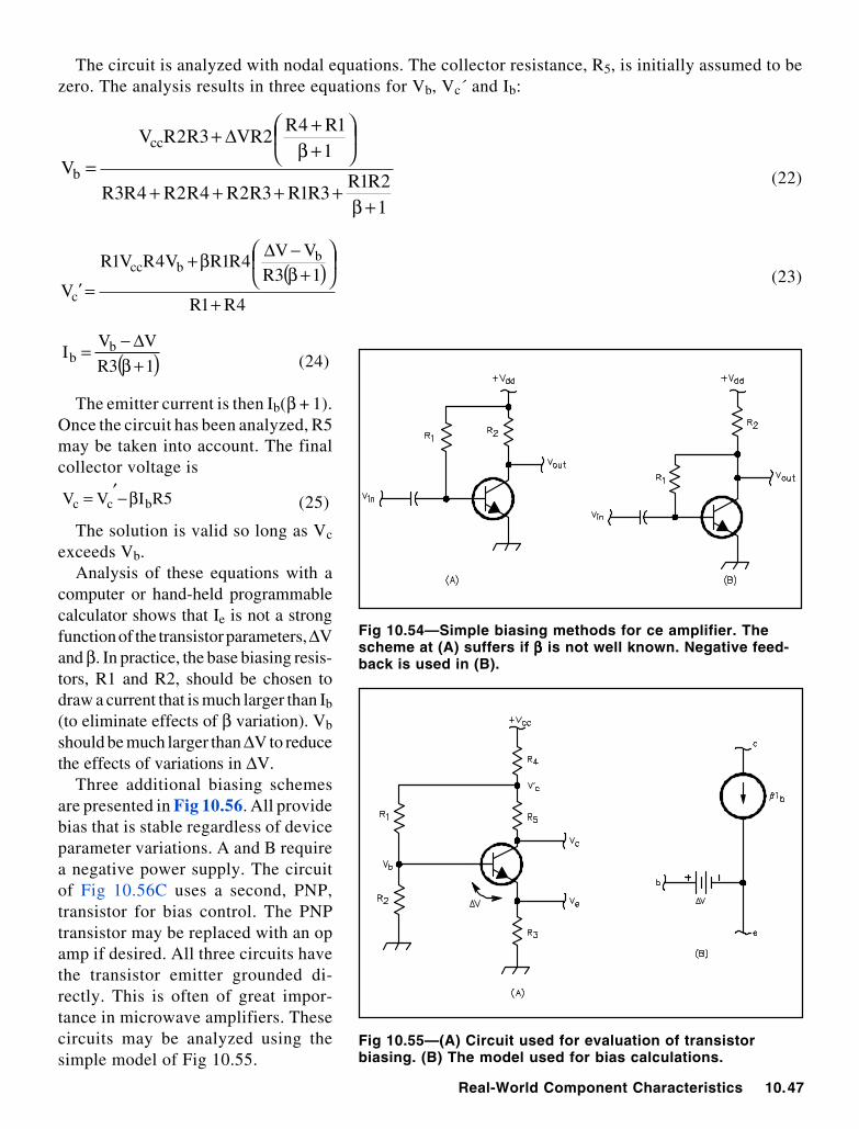
Real-World Component Characteristics 10.47
Fig 10.55—(A) Circuit used for evaluation of transistorbiasing. (B) The model used for bias calculations.
Fig 10.54—Simple biasing methods for ce amplifier. Thescheme at (A) suffers if βββββ is not well known. Negative feed-back is used in (B).
The circuit is analyzed with nodal equations. The collector resistance, R5, is initially assumed to bezero. The analysis results in three equations for Vb, Vc´ and Ib:
12R1R
3R1R3R2R4R2R4R3R
11R4R
2VR3R2RV
V
cc
b
+β++++
+β+∆+
= (22)
( )4R1R
13RVV
4R1RV4RV1R
V
bbcc
c +
+β−∆β+
='(23)
( )13R
VVI b
b +β∆−= (24)
The emitter current is then Ib(β + 1).Once the circuit has been analyzed, R5may be taken into account. The finalcollector voltage is
5RIVV bcc β−′= (25)
The solution is valid so long as Vc
exceeds Vb.Analysis of these equations with a
computer or hand-held programmablecalculator shows that Ie is not a strongfunction of the transistor parameters, ∆Vand β. In practice, the base biasing resis-tors, R1 and R2, should be chosen todraw a current that is much larger than Ib
(to eliminate effects of β variation). Vb
should be much larger than ∆V to reducethe effects of variations in ∆V.
Three additional biasing schemesare presented in Fig 10.56. All providebias that is stable regardless of deviceparameter variations. A and B requirea negative power supply. The circuitof Fig 10.56C uses a second, PNP,transistor for bias control. The PNPtransistor may be replaced with an opamp if desired. All three circuits havethe transistor emitter grounded di-rectly. This is often of great impor-tance in microwave amplifiers. Thesecircuits may be analyzed using thesimple model of Fig 10.55.
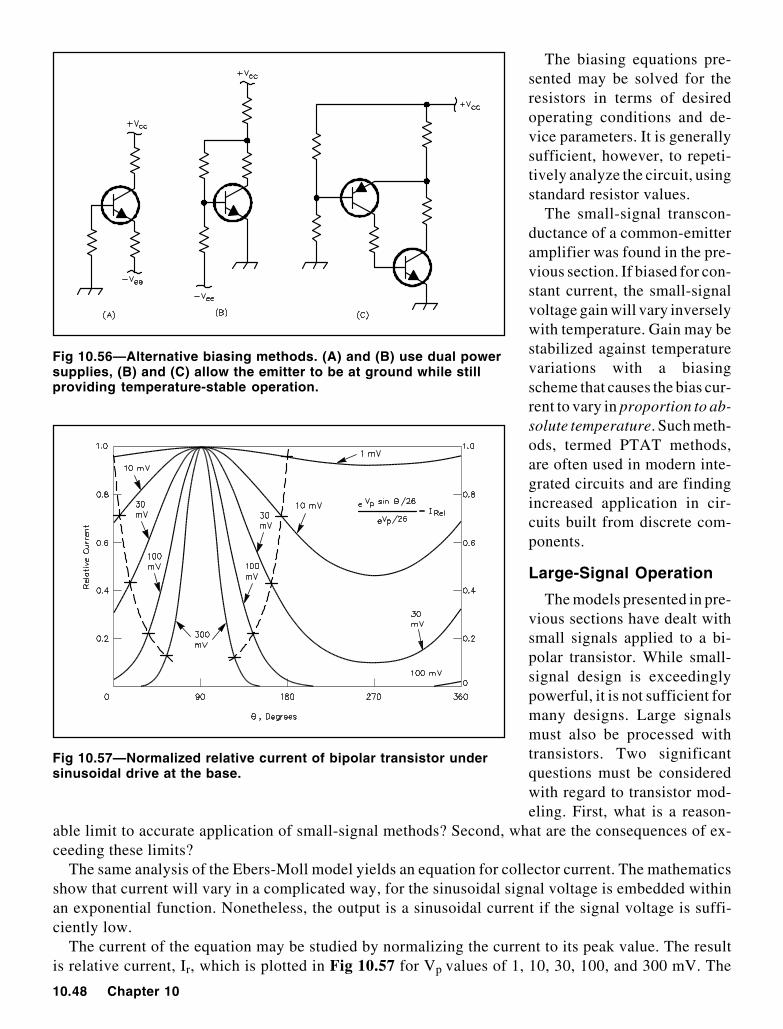
10.48 Chapter 10
Fig 10.57—Normalized relative current of bipolar transistor undersinusoidal drive at the base.
Fig 10.56—Alternative biasing methods. (A) and (B) use dual powersupplies, (B) and (C) allow the emitter to be at ground while stillproviding temperature-stable operation.
The biasing equations pre-sented may be solved for theresistors in terms of desiredoperating conditions and de-vice parameters. It is generallysufficient, however, to repeti-tively analyze the circuit, usingstandard resistor values.
The small-signal transcon-ductance of a common-emitteramplifier was found in the pre-vious section. If biased for con-stant current, the small-signalvoltage gain will vary inverselywith temperature. Gain may bestabilized against temperaturevariations with a biasingscheme that causes the bias cur-rent to vary in proportion to ab-solute temperature. Such meth-ods, termed PTAT methods,are often used in modern inte-grated circuits and are findingincreased application in cir-cuits built from discrete com-ponents.
Large-Signal Operation
The models presented in pre-vious sections have dealt withsmall signals applied to a bi-polar transistor. While small-signal design is exceedinglypowerful, it is not sufficient formany designs. Large signalsmust also be processed withtransistors. Two significantquestions must be consideredwith regard to transistor mod-eling. First, what is a reason-
able limit to accurate application of small-signal methods? Second, what are the consequences of ex-ceeding these limits?
The same analysis of the Ebers-Moll model yields an equation for collector current. The mathematicsshow that current will vary in a complicated way, for the sinusoidal signal voltage is embedded withinan exponential function. Nonetheless, the output is a sinusoidal current if the signal voltage is suffi-ciently low.
The current of the equation may be studied by normalizing the current to its peak value. The resultis relative current, Ir, which is plotted in Fig 10.57 for Vp values of 1, 10, 30, 100, and 300 mV. The
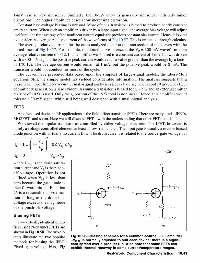
Real-World Component Characteristics 10.49
1-mV case is very sinusoidal. Similarly, the 10-mV curve is generally sinusoidal with only minordistortions. The higher amplitude cases show increasing distortion.
Constant base-voltage biasing is unusual. More often, a transistor is biased to produce nearly constantemitter current. When such an amplifier is driven by a large input signal, the average bias voltage will adjustitself until the time average of the nonlinear current equals the previous constant bias current. Hence, it is vitalto consider the average relative current of the waveforms of Fig 10.57. This is evaluated through calculus.
The average relative currents for the cases analyzed occur at the intersection of the curves with thedotted lines of Fig 10.57. For example, the dotted curve intersects the Vp = 300-mV waveform at anaverage relative current of 0.12. If an amplifier was biased to a constant current of 1 mA, but was drivenwith a 300-mV signal, the positive peak current would reach a value greater than the average by a factorof 1/(0.12). The average current would remain at 1 mA, but the positive peak would be 8 mA. Thetransistor would not conduct for most of the cycle.
The curves have presented data based upon the simplest of large-signal models, the Ebers-Mollequation. Still, the simple model has yielded considerable information. The analysis suggests that areasonable upper limit for accurate small-signal analysis is a peak base signal of about 10 mV. The effectof emitter degeneration is also evident. Assume a transistor is biased for re = 5 Ω and an external emitterresistor of 10 Ω is used. Only the re portion of the 15 Ω total is nonlinear. Hence, this amplifier wouldtolerate a 30-mV signal while still being well described with a small-signal analysis.
FETS
An often used device in RF applications is the field-effect transistor (FET). There are many kinds: JFETs,MOSFETs and so on. Here we will discuss JFETs, with the understanding that other FETs are similar.
We viewed the bipolar transistor as controlled by either voltage or current. The JFET, however, ispurely a voltage controlled element, at least at low frequencies. The input gate is usually a reverse biaseddiode junction with virtually no current flow. The drain current is related to the source-gate voltage by:
psgD
psg
2
p
sgDSSD
VV0I
VV0V
V1II
>=
≤≤
−=
(26)
where IDSS is the drain satura-tion current and Vp is the pinch-off voltage. Operation is notdefined when Vsg is less thanzero because the gate diode isthen forward biased. Equation26 is a reasonable approxima-tion as long as the drain biasvoltage exceeds the magnitudeof the pinch-off voltage.
Biasing FETs
Two virtually identical ampli-fiers using N-channel JFETs areshown in Fig 10.58. The two cir-cuits illustrate the two popularmethods for biasing the JFET.Fixed gate-voltage bias, Fig
Fig 10.58—Biasing schemes for a common-source JFET amplifier.–Vbias is normally adjusted to suit each device; there is a signifi-cant spread over a product run. Also note that some FETs canexhibit thermal runaway in some current/temperature ranges.
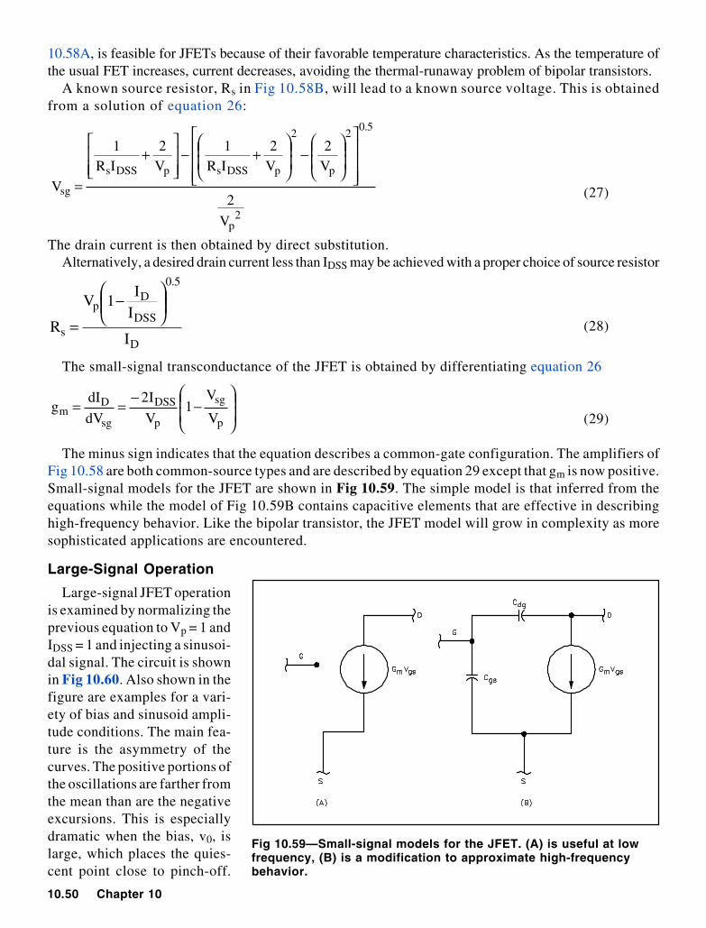
10.50 Chapter 10
10.58A, is feasible for JFETs because of their favorable temperature characteristics. As the temperature ofthe usual FET increases, current decreases, avoiding the thermal-runaway problem of bipolar transistors.
A known source resistor, Rs in Fig 10.58B, will lead to a known source voltage. This is obtainedfrom a solution of equation 26:
2p
5.02
p
2
pDSSspDSSs
sg
V
2
V2
V2
IR1
V2
IR1
V
−
+−
+
= (27)
The drain current is then obtained by direct substitution.Alternatively, a desired drain current less than IDSS may be achieved with a proper choice of source resistor
D
5.0
DSS
Dp
s I
II
1V
R
−
= (28)
The small-signal transconductance of the JFET is obtained by differentiating equation 26
−−==
p
sg
p
DSS
sg
Dm V
V1
V
I2
dV
dIg
(29)
The minus sign indicates that the equation describes a common-gate configuration. The amplifiers ofFig 10.58 are both common-source types and are described by equation 29 except that gm is now positive.Small-signal models for the JFET are shown in Fig 10.59. The simple model is that inferred from theequations while the model of Fig 10.59B contains capacitive elements that are effective in describinghigh-frequency behavior. Like the bipolar transistor, the JFET model will grow in complexity as moresophisticated applications are encountered.
Large-Signal Operation
Large-signal JFET operationis examined by normalizing theprevious equation to Vp = 1 andIDSS = 1 and injecting a sinusoi-dal signal. The circuit is shownin Fig 10.60. Also shown in thefigure are examples for a vari-ety of bias and sinusoid ampli-tude conditions. The main fea-ture is the asymmetry of thecurves. The positive portions ofthe oscillations are farther fromthe mean than are the negativeexcursions. This is especiallydramatic when the bias, v0, islarge, which places the quies-cent point close to pinch-off.
Fig 10.59—Small-signal models for the JFET. (A) is useful at lowfrequency, (B) is a modification to approximate high-frequencybehavior.
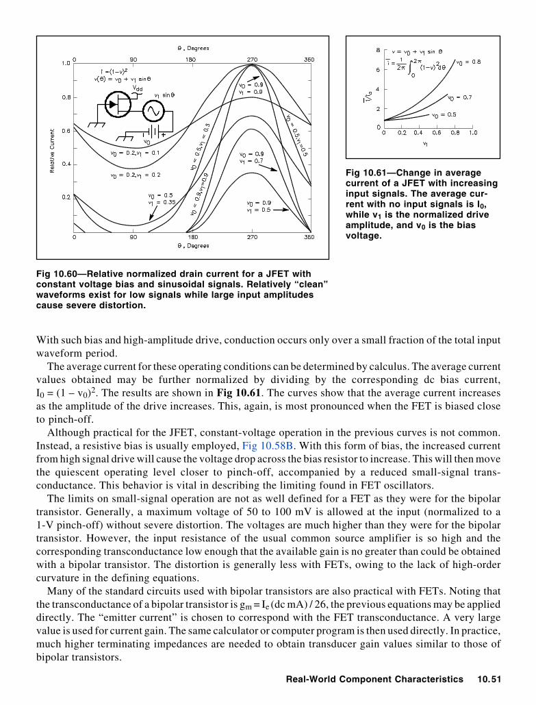
Real-World Component Characteristics 10.51
With such bias and high-amplitude drive, conduction occurs only over a small fraction of the total inputwaveform period.
The average current for these operating conditions can be determined by calculus. The average currentvalues obtained may be further normalized by dividing by the corresponding dc bias current,I0 = (1 – v0)2. The results are shown in Fig 10.61. The curves show that the average current increasesas the amplitude of the drive increases. This, again, is most pronounced when the FET is biased closeto pinch-off.
Although practical for the JFET, constant-voltage operation in the previous curves is not common.Instead, a resistive bias is usually employed, Fig 10.58B. With this form of bias, the increased currentfrom high signal drive will cause the voltage drop across the bias resistor to increase. This will then movethe quiescent operating level closer to pinch-off, accompanied by a reduced small-signal trans-conductance. This behavior is vital in describing the limiting found in FET oscillators.
The limits on small-signal operation are not as well defined for a FET as they were for the bipolartransistor. Generally, a maximum voltage of 50 to 100 mV is allowed at the input (normalized to a1-V pinch-off) without severe distortion. The voltages are much higher than they were for the bipolartransistor. However, the input resistance of the usual common source amplifier is so high and thecorresponding transconductance low enough that the available gain is no greater than could be obtainedwith a bipolar transistor. The distortion is generally less with FETs, owing to the lack of high-ordercurvature in the defining equations.
Many of the standard circuits used with bipolar transistors are also practical with FETs. Noting thatthe transconductance of a bipolar transistor is gm = Ie (dc mA) / 26, the previous equations may be applieddirectly. The “emitter current” is chosen to correspond with the FET transconductance. A very largevalue is used for current gain. The same calculator or computer program is then used directly. In practice,much higher terminating impedances are needed to obtain transducer gain values similar to those ofbipolar transistors.
Fig 10.60—Relative normalized drain current for a JFET withconstant voltage bias and sinusoidal signals. Relatively “clean”waveforms exist for low signals while large input amplitudescause severe distortion.
Fig 10.61—Change in averagecurrent of a JFET with increasinginput signals. The average cur-rent with no input signals is I0,while v1 is the normalized driveamplitude, and v0 is the biasvoltage.
10.52 Chapter 10
References
1. Ebers, J., and Moll, J., “Large-Signal Behavior of Junction Transistors,” Proceedings of the IRE, 42,pp 1761-1772, December 1954.
2. Getreu, I., Modeling the Bipolar Transistor, Elsevier, New York, 1979. Also available from Tektronix,Inc, Beaverton, Oregon, in paperback form. Must be ordered as Part Number 062-2841-00.
3. Searle, C., Boothroyd, A., Angelo, E. Jr., Gray, P., and Pederson, D., Elementary Circuit Propertiesof Transistors, Semiconductor Electronics and Education Committee, Vol 3, John Wiley & Sons,New York, 1964.
4. Clarke, K. and Hess, D., Communication Circuits: Analysis and Design, Addison-Wesley, Reading,Massachusetts, 1971.
5. Middlebrook, R., Design-Oriented Circuit Analysis and Measurement Techniques. Copyrighted notesfor a short course presented by Dr Middlebrook in 1978.
Suggested Additional Readings
Alley, C. and Atwood, K., Electronic Engineering, John Wiley & Sons, New York, 1962.Terman, F., Electronic and Radio Engineering, McGraw-Hill, New York, 1955.Gilbert, B., “A New Wide-Band Amplifier Technique,” IEEE Journal of Solid-State Circuits, SC-3, 4,
pp 353-365, December 1968.Egenstafer, F., “Design Curves Simplify Amplifier Analysis,” Electronics, pp 62-67, August 2, 1971.