Embed Size (px)
Citation preview
Novel Syntheses of Thermoelectric and Nanostructured Materials and a
System for Purifying and Sorting Metallic and Semiconducting Single-
Walled Carbon Nanotubes in a Mixed-Tube Suspension
by
Su (Ike) Chih Chi
A dissertation submitted to The Johns Hopkins University in conformity
with the requirements for the degree of Doctor of Philosophy
© 2014
Su C. Chi
All Rights Reserved
ii
Abstract
The integration of materials science and engineering at the nanoscale has significant
impact in many areas of science and technology. In this dissertation, I will present novel
syntheses of lanthanum telluride thermoelectric materials, vertically-aligned nanowires,
and nanoporous nickel membranes. I will also present a method that can collect
industrially relevant quantity of purified and sorted metallic and semiconducting single-
walled carbon nanotubes (SWCNTs) in a mixed-carbon nanotubes suspension by AC
dielectrophoresis.
In the Chapter 1: A Novel Approach to Synthesize Lanthanum Telluride
Thermoelectric Materials, I will report on the electrochemical synthesis of lanthanum
telluride thin films. The electrodeposition of lanthanum telluride thin films is performed
in a room-temperature ionic liquid, 1-ethyl-3-methylimidazolium bromide (EMIB), in
ambient conditions. This novel procedure can serve as an alternative means of simple,
inexpensive, and laboratory-environment friendly methods to synthesize rare-earth
telluride thermoelectric materials that were difficult to make in aqueous solution.
Characterization of the morphologies and chemical compositions of the deposited films
using scanning electron microscopy (SEM), x-ray diffractometry (XRD), and energy-
dispersive x-ray analysis (EDAX) will be presented. The Seebeck coefficient and
iii
electrical resistivity of deposited lanthanum telluride thin films will also be presented and
compared with those of current state-of-the-art thermoelectric materials.
In the Chapter 2: Synthesis and Characterization of Vertically-aligned Gold
Nanowires Arrays Ferromagnetic Composite Films, I will report on the electrochemical
synthesis of films composed of vertically-aligned gold nanowire arrays in ferromagnetic
matrices (nickel and iron). This process involves first electrodepositing the Au nanowire
arrays within commercially available anodic aluminum oxide (AAO) nanoporous
membranes. After dissolving the templates, the ferromagnetic matrices are grown around
the nanowires to produce the two-phase nanocomposites.
In the Chapter 3: A Novel Approach to the Synthesis of Nanochanneled Nickel
Films, I will report on an innovative technique to fabricate nickel nanochanneled
membranes. This procedure involves transferring and imprinting the nanoporous arrays
of the AAO membranes to a nickel film using a template-guided electrochemical etching
technique. A detailed discussion of these processing techniques will be shown along with
the characterization of the morphology of nickel nanochanneled membranes.
Lastly, in the Chapter 4: Purification and Refinement of Single-Walled Carbon
Nanotubes (SWCNTs) by AC Dielectrophoresis (DEP), a continuous flow device for
purifying and sorting metallic and semiconducting SWCNTs from an initially random
mixture of SWCNTs in suspension using AC dielectrophoresis is reported. The
separation of two electronic types of SWCNTs takes advantage of the large difference of
the relative dielectric constants between metallic and semiconducting SWCNTs with
respect to the suspension, resulting in both a difference in magnitude and direction of a
dielectrophoretic force imposed on the SWCNTs. This work presents a significant
iv
advancement in nanotubes purification in a facile and scalable manner, and can therefore
significantly increase the feasibility of manufacturing reliable SWCNT-based
nanoelectronic devices. A detailed discussion of the sorting techniques will be presented
along with the fabrication of a dielectrophoretic force utilized microfluidic lab-on-a-chip
device that can continuously refine and collect metallic and nonmetallic nanoparticles at
industrially relevant processing rates. The effectiveness of the device is characterized
using resonant Raman and ultraviolet–visible-near infrared (UV-Vis-NIR) spectroscopy
analysis on sorted samples.

v
To my parents and my sister for their unconditional supports and sacrifices during the
years of my Ph.D. study

vi
Acknowledgments
Firstly, I would like to thank my parents, Hsien-Ling Wei and Kuo-Ching Chi and my
sister, Dr. Sabrina Su-Li Chi for their unconditional supports and sacrifices throughout
the years of my Ph.D. study.
I would like to especially thank to my research advisor, Prof. Robert C.
Cammarata for his guidance and constant support on my research works as well as many
regarding life in general. I am especially grateful to my committee members: Prof. Jonah
Erlebacher and Prof. En Ma of Department of Materials Science and Engineering and
Prof. Chia-Ling Chien of Department of Physics and Astronomy and and Prof. Howard
Fairbrother of Department of Chemistry for their kindness and useful discussions during
my thesis defense. I am also very grateful to the funding support from Prof. Chia-Ling
Chien of Department of Physics and Astronomy.
I would also like to thank current and previous Cammarata group’s members: Mr.
Stephen Farias, Mr. Austin Young, Mr. Nicholas Dee, and Mr. Rustin Golnabi for their
kindly supports on my research works in general throughout the years of my Ph.D. study
in Baltimore, MD. I would like to especially thank to Mr. Stephen Farias again for his
role as my initial mentor and then numerous valuable discussions on my research works
as well as regarding life in general.
vii
I would like to thank Ms. Danru Qu of Johns Hopkins University for the initial
collaborations of the carbon nanotubes separation project. I am also very indebted to her
kindness and unconditional supports for conducting many property measurements and
helping me with material syntheses. Without her help, my thesis work would become
much more problematic. I would also like to thank Dr. Sunxiang Huang and Mr. Mingen
Li of Johns Hopkins University for preforming many material’s property measurements
on the samples I synthesized.
I would like to appreciatively thank to Mr. Yu-Ja Huang of Johns Hopkins
University for training me the techniques of microfabrication and coaching me valuable
knowledge regarding microfluidic devices made of polydimethylsiloxane (PDMS). I am
very thankful to Dr. Maya Zayats of Johns Hopkins University to get me the access of the
cleanroom in her lab. I am also gratefully thank my officemate, Mr. Samuel Rosenthal,
for many helpful discussions on the technical issues of my thesis works as well as
regarding life in general throughout the last two years of my Ph.D. study.
I would like to gratefully thank Mr. Ming-Ling Yeh of Johns Hopkins University
for performing Seebeck coefficient and electrical resistance measurements of the
electrodeposited Lanthanum Telluride films and many useful discussions regarding my
research works throughout the years of my Ph.D. study. I am very grateful to Dr.
Kailiang Ren, Dr. Weiguo Huang, and Mr. Yu Liu of Johns Hopkins University for many
valuable discussions on my technical issues as well as regarding life in general. My lunch
would not be the same without your guys.
I would like to thank Mr. Ian McCue of Johns Hopkins University for many
useful discussions regarding the preparation and the chemistry of room temperature ionic
viii
liquids. I would also like to thank Prof. Todd C. Hufnagel of Johns Hopkins University
for valuable discussions regarding X-ray diffraction pattern of the electrodeposited
Lanthanum Telluride films. Ms. Mantong Zhao of Johns Hopkins University is also
acknowledged for many useful discussions regarding X-ray diffraction pattern in general.
I would like to acknowledge Dr. Shaka Prokes, Dr. Joshua Caldwell, and Dr.
Konrad Bussmann of Naval Research Laboratory and Dr. Natalia Drichko of Johns
Hopkins University for performing the resonant Raman studies of separated single-walled
carbon nanotubes (SWCNTs) from the static system. Ms. Sarvenaz Sarabipour of Johns
Hopkins University and Dr. Jesse Placone of currently University of Maryland are
acknowledged for allowing me to have access to the equipment of their lab. Dr. Yong
Ren of Johns Hopkins University is acknowledged for getting me the access of the
ultraviolet-visible (UV-Vis) spectrophotometry of his lab. I would like to gratefully thank
to Dr. Xuan Jiang and Mr. Deng Pan for their kindness for helping me regarding the
knowledge of biological materials throughout the first two years of my Ph.D. study.
I would like to gratefully thank Mr. Mark Koontz of Johns Hopkins University for
assistance with the scanning electron microscopy (SEM) as well as regarding lots of
hardware troubleshooting in general throughout the years of my Ph.D. study. I also want
to thank Ms. Marge Weaver and Ms. Dorothy Reagle for their wholehearted supports
throughout the years of my Ph.D. study. I would also like to gratefully thank Ms. Jeanine
Majewski for her kindness to make my thesis defense pleasantly happen.
ix
Contents
Abstract…………………………………………………………………………………...i
Acknowledgments………………………………………………………………………..v
List of Tables……………………………………………………………………………..x
List of Figures……………………………………………………………………………xi
1. A Novel Approach to Synthesize Lanthanum Telluride Thermoelectric Materials 1.1 Introduction……………………………………………………………………...1
1.1.1 Thermoelectric Figure of Merit (ZT)……………………………………3 1.1.2 Lanthanum Telluride (La3-xTe4) Thermoelectric Material……………...9 1.1.3 Room Temperature Ionic Liquids (RTILs)…………………………….12
1.2 Experimental…………………………………………………………....……...14 1.3 Results and Discussion………………………………………………………...18 1.4 Conclusions…………………………………………………………………….23 1.5 Future Work……………………………………………………………………23 Bibliography…………………………………………………………………………25
2. Synthesis and Characterization of Vertically-aligned Gold Nanowires Arrays Ferromagnetic Composite Films 2.1 Introduction…………………………………………………………………….30
2.1.1 Localized Surface Plasmon Resonance (LSPR)…………….................31 2.2 Experimental…………………………………………………………………...34 2.3 Results and Discussion………………………………………………………...36 2.4 Conclusions…………………………………………………………………….40 2.5 Future Work……………………………………………………………………41 Bibliography…………………………………………………………………………42
3. A Novel Approach to the Synthesis of Nanochanneled Nickel Films 3.1 Introduction…………………………………………………………………….443.2 Experimental…………………………………………………………………...46 3.3 Results and Discussion………………………………………………………...47 3.4 Conclusions…………………………………………………………………….50 3.5 Future Work……………………………………………………………………51 Bibliography…………………………………………………………………………52
x
4. Purification and Refinement of Single-Walled Carbon Nanotubes (SWCNTs) by AC Dielectrophoresis 4.1 Introduction…………………………………………………………………….55
4.1.1 Single-Walled Carbon Nanotubes (SWCNTs)………………………...57 4.1.2 AC Dielectrophoresis on Single-Walled Carbon Nanotubes………….61
4.1.3 Understanding Electronic Types of SWCNTs from their Resonant Raman Features………………………………………………………...66
4.2 Experimental…………………………………………………………………...68 4.2.1 Static System…………………………………………………………...68 4.2.2 Continuous Flow System………………………………………………70
4.3 Results and Discussion………………………………………………………...80 4.3.1 Static System…………………………………………………………...80 4.3.2 Continuous Flow System………………………………………………88
4.4 Conclusions………………………………………………………………….....944.5 Future Work……………………………………………………………………95 Bibliography…………………………………………………………………………98
5. Summary…………………………………………………………………………...105
A List of Publications and Patents…………………………………………………...108
A List of Conference Presentations and Poster Sessions……………………………109
xi
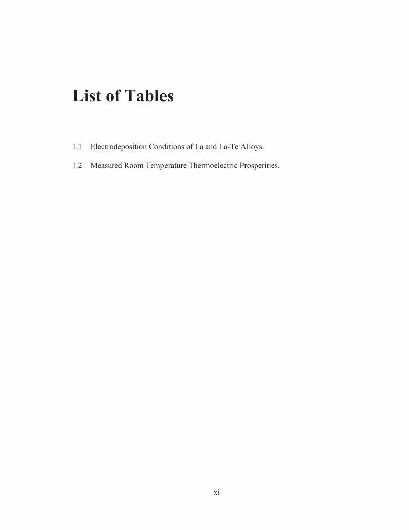
List of Tables
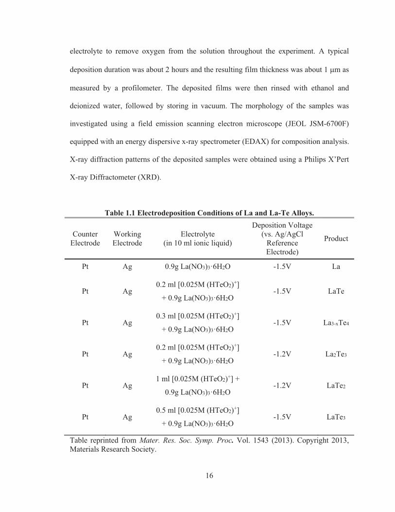
1.1 Electrodeposition Conditions of La and La-Te Alloys.
1.2 Measured Room Temperature Thermoelectric Prosperities.
xii
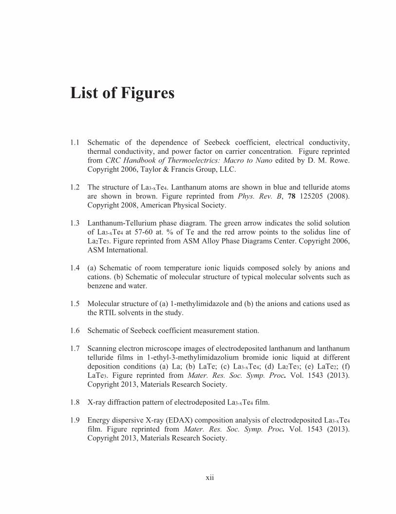
List of Figures
1.1 Schematic of the dependence of Seebeck coefficient, electrical conductivity, thermal conductivity, and power factor on carrier concentration. Figure reprinted from CRC Handbook of Thermoelectrics: Macro to Nano edited by D. M. Rowe. Copyright 2006, Taylor & Francis Group, LLC.
1.2 The structure of La3-xTe4. Lanthanum atoms are shown in blue and telluride atoms are shown in brown. Figure reprinted from Phys. Rev. B, 78 125205 (2008). Copyright 2008, American Physical Society.
1.3 Lanthanum-Tellurium phase diagram. The green arrow indicates the solid solution of La3-xTe4 at 57-60 at. % of Te and the red arrow points to the solidus line of La2Te3. Figure reprinted from ASM Alloy Phase Diagrams Center. Copyright 2006, ASM International.
1.4 (a) Schematic of room temperature ionic liquids composed solely by anions and cations. (b) Schematic of molecular structure of typical molecular solvents such as benzene and water.
1.5 Molecular structure of (a) 1-methylimidazole and (b) the anions and cations used as the RTIL solvents in the study.
1.6 Schematic of Seebeck coefficient measurement station.
1.7 Scanning electron microscope images of electrodeposited lanthanum and lanthanum telluride films in 1-ethyl-3-methylimidazolium bromide ionic liquid at different deposition conditions (a) La; (b) LaTe; (c) La3-xTe4; (d) La2Te3; (e) LaTe2; (f) LaTe3. Figure reprinted from Mater. Res. Soc. Symp. Proc. Vol. 1543 (2013). Copyright 2013, Materials Research Society.
1.8 X-ray diffraction pattern of electrodeposited La3-xTe4 film.
1.9 Energy dispersive X-ray (EDAX) composition analysis of electrodeposited La3-xTe4
film. Figure reprinted from Mater. Res. Soc. Symp. Proc. Vol. 1543 (2013). Copyright 2013, Materials Research Society.
xiii
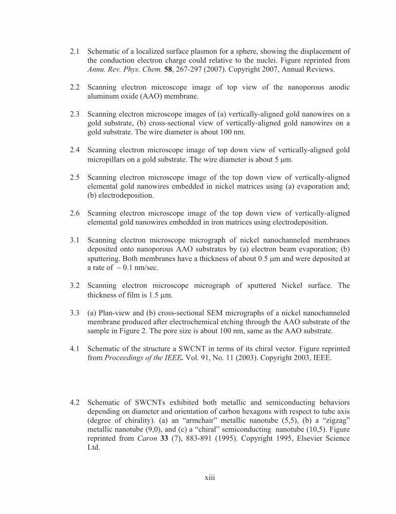
2.1 Schematic of a localized surface plasmon for a sphere, showing the displacement of the conduction electron charge could relative to the nuclei. Figure reprinted from Annu. Rev. Phys. Chem. 58, 267-297 (2007). Copyright 2007, Annual Reviews.
2.2 Scanning electron microscope image of top view of the nanoporous anodic aluminum oxide (AAO) membrane.
2.3 Scanning electron microscope images of (a) vertically-aligned gold nanowires on a gold substrate, (b) cross-sectional view of vertically-aligned gold nanowires on a gold substrate. The wire diameter is about 100 nm.
2.4 Scanning electron microscope image of top down view of vertically-aligned gold micropillars on a gold substrate. The wire diameter is about 5 �m.
2.5 Scanning electron microscope image of the top down view of vertically-aligned elemental gold nanowires embedded in nickel matrices using (a) evaporation and; (b) electrodeposition.
2.6 Scanning electron microscope image of the top down view of vertically-aligned elemental gold nanowires embedded in iron matrices using electrodeposition.
3.1 Scanning electron microscope micrograph of nickel nanochanneled membranes deposited onto nanoporous AAO substrates by (a) electron beam evaporation; (b) sputtering. Both membranes have a thickness of about 0.5 �m and were deposited at a rate of ~ 0.1 nm/sec.
3.2 Scanning electron microscope micrograph of sputtered Nickel surface. The thickness of film is 1.5 �m.
3.3 (a) Plan-view and (b) cross-sectional SEM micrographs of a nickel nanochanneled membrane produced after electrochemical etching through the AAO substrate of the sample in Figure 2. The pore size is about 100 nm, same as the AAO substrate.
4.1 Schematic of the structure a SWCNT in terms of its chiral vector. Figure reprinted from Proceedings of the IEEE. Vol. 91, No. 11 (2003). Copyright 2003, IEEE.
4.2 Schematic of SWCNTs exhibited both metallic and semiconducting behaviors depending on diameter and orientation of carbon hexagons with respect to tube axis (degree of chirality). (a) an “armchair” metallic nanotube (5,5), (b) a “zigzag” metallic nanotube (9,0), and (c) a “chiral” semiconducting nanotube (10,5). Figure reprinted from Caron 33 (7), 883-891 (1995). Copyright 1995, Elsevier Science Ltd.
xiv
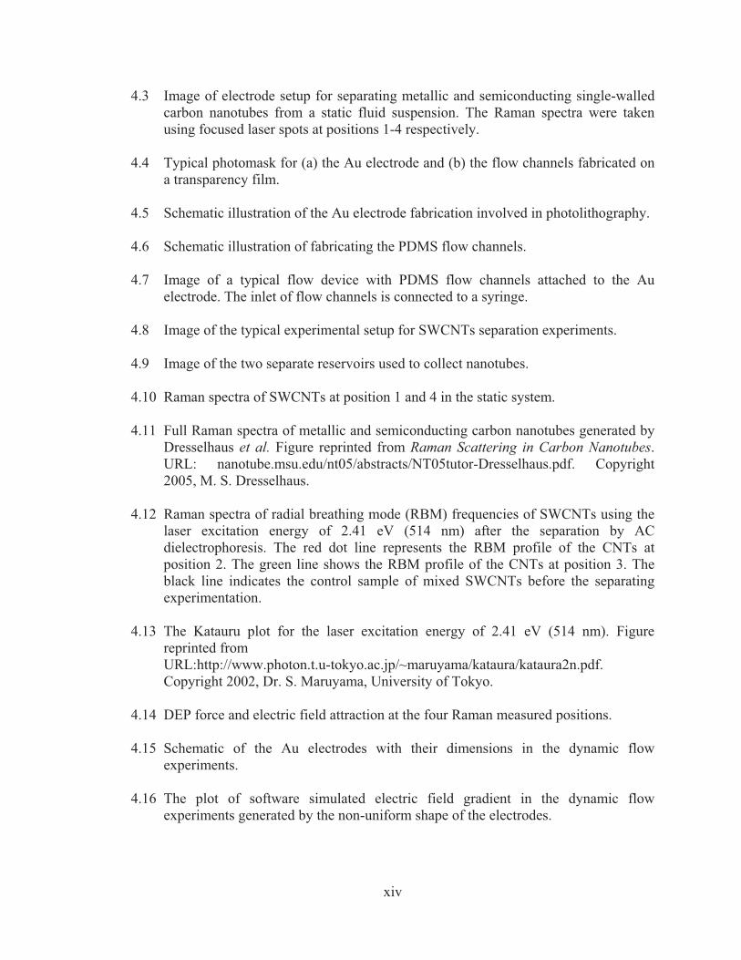
4.3 Image of electrode setup for separating metallic and semiconducting single-walled carbon nanotubes from a static fluid suspension. The Raman spectra were taken using focused laser spots at positions 1-4 respectively.
4.4 Typical photomask for (a) the Au electrode and (b) the flow channels fabricated on a transparency film.
4.5 Schematic illustration of the Au electrode fabrication involved in photolithography.
4.6 Schematic illustration of fabricating the PDMS flow channels.
4.7 Image of a typical flow device with PDMS flow channels attached to the Au electrode. The inlet of flow channels is connected to a syringe.
4.8 Image of the typical experimental setup for SWCNTs separation experiments.
4.9 Image of the two separate reservoirs used to collect nanotubes.
4.10 Raman spectra of SWCNTs at position 1 and 4 in the static system.
4.11 Full Raman spectra of metallic and semiconducting carbon nanotubes generated by Dresselhaus et al. Figure reprinted from Raman Scattering in Carbon Nanotubes.URL: nanotube.msu.edu/nt05/abstracts/NT05tutor-Dresselhaus.pdf. Copyright 2005, M. S. Dresselhaus.
4.12 Raman spectra of radial breathing mode (RBM) frequencies of SWCNTs using the laser excitation energy of 2.41 eV (514 nm) after the separation by AC dielectrophoresis. The red dot line represents the RBM profile of the CNTs at position 2. The green line shows the RBM profile of the CNTs at position 3. The black line indicates the control sample of mixed SWCNTs before the separating experimentation.
4.13 The Katauru plot for the laser excitation energy of 2.41 eV (514 nm). Figure reprinted fromURL:http://www.photon.t.u-tokyo.ac.jp/~maruyama/kataura/kataura2n.pdf.Copyright 2002, Dr. S. Maruyama, University of Tokyo.
4.14 DEP force and electric field attraction at the four Raman measured positions.
4.15 Schematic of the Au electrodes with their dimensions in the dynamic flow experiments.
4.16 The plot of software simulated electric field gradient in the dynamic flow experiments generated by the non-uniform shape of the electrodes.
xv
4.17 UV-Vis spectra showing purification of SWCNTs in the reservoir 1 at 5 Vp-p and 10MHz DEP conditions.
4.18 UV-Vis-NIR spectra showing the extension of purified SWCNTs in the reservoir 1 at 5 Vp-p and 10MHz DEP conditions.
4.19 UV-Vis-NIR spectra showing the ~7% increase in purity of semiconducting SWCNTs purity in both reservoirs at the DEP of (5 Vp-p, 500 MHz) and (5 Vp-p, 100MHz) conditions.
4.20 Image of an extra buffer channeled flow device used to flush the metallic SWCNTs attached on the inner electrode.
4.21 Schematic of potential future direction of the invited DEP derived flow device for sorting SWCNTs.
1
Chapter 1
A Novel Approach to Synthesize Lanthanum
Telluride Thermoelectric Materials
1.1 Introduction
This section is an adapted reproduction from Mater. Res. Soc. Symp. Proc. Vol. 1543
(2013). Copyright 2013, Materials Research Society.
Rare-earth elements and their telluride alloys have attracted significant attention
because of their potential applications in thermoelectrics, electronics, and
optoelectronics.1-2 In particular, lanthanum and lanthanum telluride alloys are of interest
because lanthanum is used in large quantities in nickel metal hydride (NiMH)
rechargeable batteries for hybrid automobiles. The negative electrode (cathode) in NiMH
batteries is a mixture of metal hydrides, one of which is typically lanthanum hydride. The
active material at the cathode is hydrogen, which is stored in the metal hydride
structure.3 A Toyota Prius battery requires 10 to 15 kg (22 to 33 lb) of lanthanum.4-5
Lanthanum can also be used to make the infrared-absorbing glass in night vision goggles.
High quality camera and telescope lenses contain lanthanum oxide (La2O3) making use of
its high refractive index and low dispersion.6 In addition, May and co-workers reported
that nanostructured bulk lanthanum telluride (La3-xTe4, 0 < x � ��) produced by
2
mechanical ball-milling exceeded the figure of merit (ZT) of 1 at high temperatures near
1300K.7-8 LaTe and La2Te3 are good candidates for photoconductive and photovoltaic
cells applications.9-10 LaTe2 and LaTe3 are n-type semiconductors having unique
electronic properties.9-11
Since the increased thermoelectric efficiency of nanostructured materials are due
to the enhancement of phonon scattering introduced by quantum confinement, thin films
(2-D systems) and nanowires (1-D systems) also have generated significant scientific and
technological interest.12,13-15 Here, I report on the electrochemical synthesis of lanthanum
telluride thin films. Electrochemical deposition is a very attractive process for
synthesizing thin films of compound semiconductors on metallic surfaces.16 The
thickness of thin films can be controlled by deposition duration. An advantage of this
technique is that it is a simple, inexpensive, and laboratory-environment friendly
synthesis methods for telluride based thermoelectric materials.
Producing thick rare-earth telluride films can be very material consuming when
using physical vapor deposition methods such as sputtering or evaporation, but films of
several microns thickness can be produced in a few hours using electrochemical
deposition. In addition, variations in the deposition potential or solution concentration
can provide different molar ratios of La-Te. It is important to note that aqueous solutions
are not preferred for lanthanum alloy electrodeposition because hydrogen evolution can
occur before the deposition of metals. Recently, room-temperature ionic liquids (RTILs)
have attracted significant attention in the electrodeposition of rare-earth metals in
ambient conditions.17-18 Here, I report on the electrodeposition of lanthanum and
lanthanum telluride alloys in a ionic liquid, 1-ethyl-3-methylimidazolium bromide
3
(EMIB), which has the advantages of good cathodic stability, low hygroscopy, and low
reactivity with oxygen and moisture.
1.1.1 Thermoelectric Figure of Merit (ZT)
Thermoelectric generators (TEGs) can be treated as Carnot cycle engines, but
instead of a gas or liquid, the working fluid is electrons.19-21 The maximum efficiency of
an thermoelectric generator is related to both the product of the Carnot efficiency and a
thermoelectric material properties depended parameter known as figure of merit (ZT).
���� � ��
����� �������
, (1.1)
where �max is the maximum efficiency of the thermoelectric generator, TH is the
temperature at the hot junction, and TC is the temperature where the surface is getting
cooled.19-21 The thermoelectric figure of merit (ZT) is a dimensionless parameter that is
related to three material transport properties. ZT is written as
�� � ���� �, (1.2)
where S is the Seebeck coefficient (�V/K), � is the electrical resistivity (m�-cm), � is the
thermal conductivity (W/mK), and T is the absolute operating temperature (K).19-21
Sometimes, the performance of a thermoelectric material can be referred to its power
4
factor in thermoelectric generation applications. The power factor, P (W M-1 K-2), can be
expressed as
� � ��� , (1.3)
where S is the Seebeck coefficient (�V/K) and � is the electrical resistivity (m�-cm).19-21
The thermal conductivity, �, can be expressed as �el + �lat, where �el is the electronic
thermal conductivity and �lat is the lattice thermal conductivity.22 Thermoelectric
materials with high power factors can generate more energy from the thermoelectric
effect, but they are not necessarily very efficient. This can be understood using Fourier’s
law of thermal conduction, for the heat flow � � �� ���. For a given heat flux, when a
thermoelectric material has a large thermal gradient from that heat flux and the thermal
conductivity of that material is low, the material is considered thermoelectric efficient.19-
20
The Seebeck coefficient, S, is a material property that characterizes the response
of the net diffusion of electrons to a thermal gradient. Mathematically, the coefficient is
represented as
� � ��, (1.4)
where V is the measured voltage change across a material when a thermal gradient is
applied to the material and �T is the temperature difference due to the thermal gradient.19-
5
20 The Seebeck coefficient is negative when the material is an n-type semiconductor
because the direction of electric current is opposite to the direction of thermal diffusion.
On the other hand, when a material is a p-type semiconductor, its Seebeck coefficient is
positive because the direction of electric current is the same as the direction of thermal
diffusion.19-20
Since all three parameters (Seebeck coefficient, electrical resistivity, and thermal
conductivity) that appear in the figure of merit (ZT) are functions of carrier concentration,
it is important to understand the interrelationship between carrier concentration and the
three material transport properties. Electrical resistivity is an important parameter to
determine the thermoelectric properties of materials. Metals usually have a low electrical
resistivity, while that of insulators is high and that of semiconductors is intermediate
between that of metals and insulators. In most textbooks and references, electrical
resistivity is usually reported and discussed by its inverse parameters, electrical
conductivity, which is represented as,
�� � �, (1.5)
where � is electrical resistivity and � is electrical conductivity.
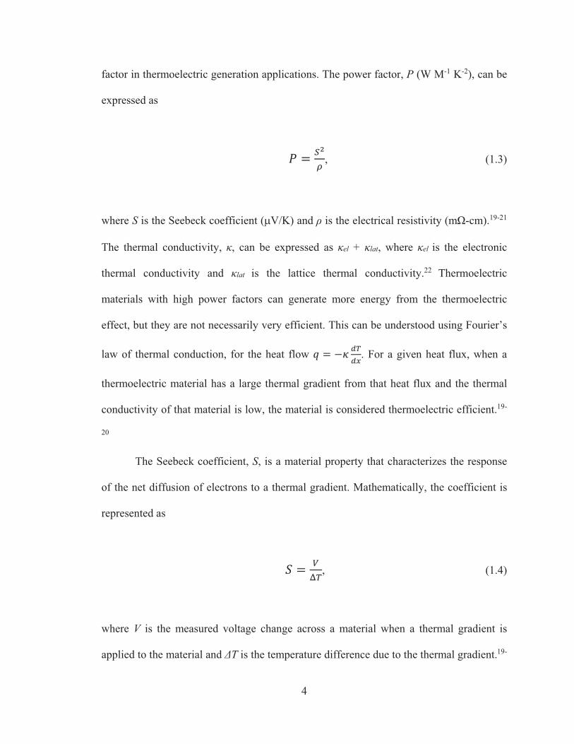
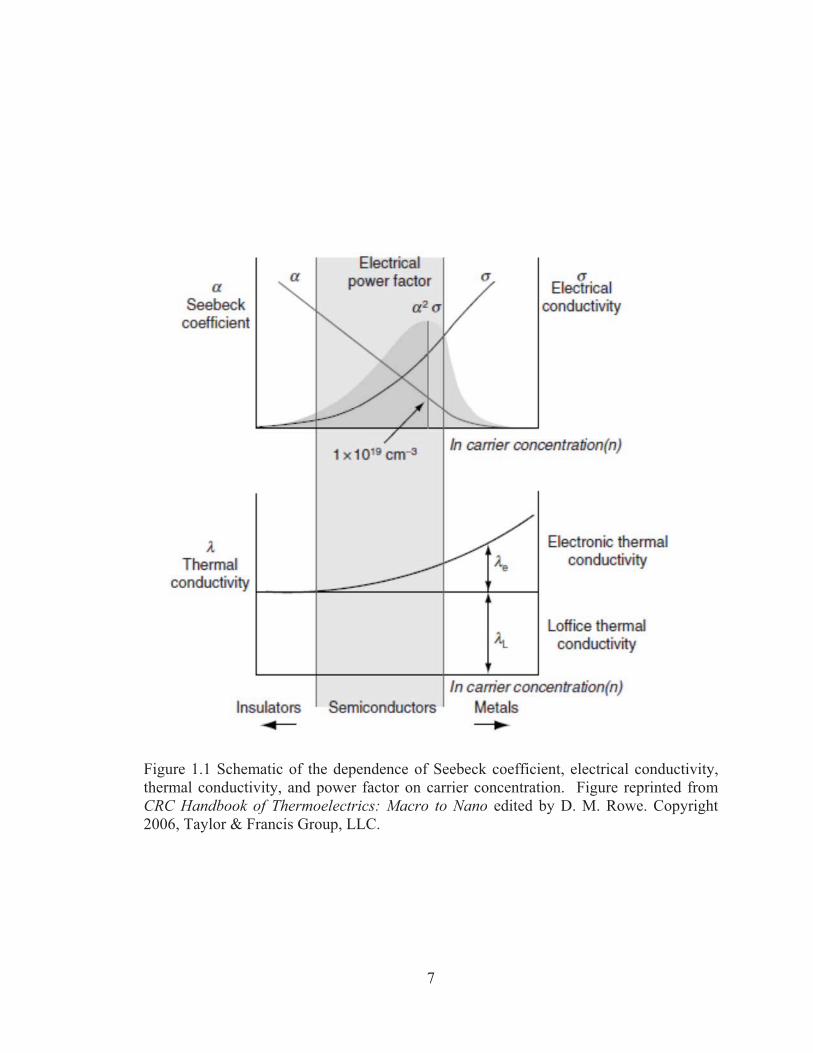
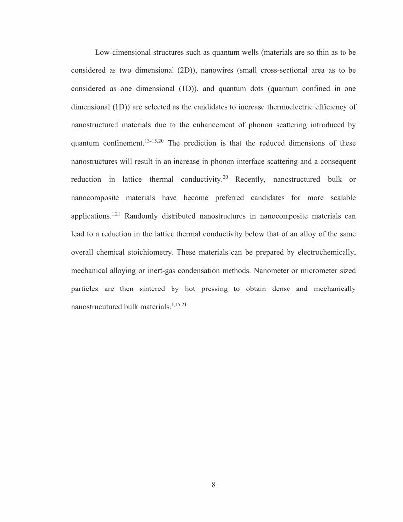
Referring to Figure 1.1 reprinted from CRC Handbook of Thermoelectrics: Macro
to Nano edited by D. M. Rowe, one can understand that in order to optimizing the power
factor of a thermoelectric material, it is necessary to find the right balance between
Seebeck coefficient and electrical conductivity of that material, since a low carrier
concentration results in a low electrical conductivity of the material but large Seebeck
6
coefficient.20,22 In addition, the electronic contribution to the thermal conductivity, �el,
which is generally about �� of the total thermal conductivity, also increases with carrier
concentration.20
For the past 20 years, the enhancement of the thermoelectric figure of merit (ZT)
has been predicted and demonstrated through nanostructural engineering.12,22-23 Efforts
have focused on improving the figure of merit (ZT) by reducing lattice thermal
conductivity. Three research avenues have been predicted to achieve the increase of ZT.
One is search for so-called “phonon glass electronic crystals” in which it is proposed that
crystal structures containing weakly bound atoms or molecules that “rattle” within an
atomic cage should conduct heat like a glass, but conduct electricity like a crystal.2
Materials attracting attention usually have disorder and complexity within their unit cell,
such as skutterudites,20,22,24 calthrates,20,22,25 and Zintl phases.22-23
7
Figure 1.1 Schematic of the dependence of Seebeck coefficient, electrical conductivity, thermal conductivity, and power factor on carrier concentration. Figure reprinted from CRC Handbook of Thermoelectrics: Macro to Nano edited by D. M. Rowe. Copyright 2006, Taylor & Francis Group, LLC.
8
Low-dimensional structures such as quantum wells (materials are so thin as to be
considered as two dimensional (2D)), nanowires (small cross-sectional area as to be
considered as one dimensional (1D)), and quantum dots (quantum confined in one
dimensional (1D)) are selected as the candidates to increase thermoelectric efficiency of
nanostructured materials due to the enhancement of phonon scattering introduced by
quantum confinement.13-15,20 The prediction is that the reduced dimensions of these
nanostructures will result in an increase in phonon interface scattering and a consequent
reduction in lattice thermal conductivity.20 Recently, nanostructured bulk or
nanocomposite materials have become preferred candidates for more scalable
applications.1,21 Randomly distributed nanostructures in nanocomposite materials can
lead to a reduction in the lattice thermal conductivity below that of an alloy of the same
overall chemical stoichiometry. These materials can be prepared by electrochemically,
mechanical alloying or inert-gas condensation methods. Nanometer or micrometer sized
particles are then sintered by hot pressing to obtain dense and mechanically
nanostrucutured bulk materials.1,15,21
9
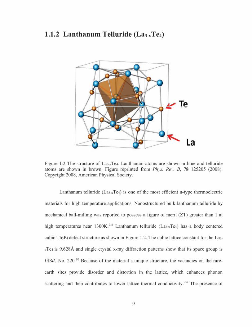
1.1.2 Lanthanum Telluride (La3-xTe4)
Figure 1.2 The structure of La3-xTe4. Lanthanum atoms are shown in blue and telluride atoms are shown in brown. Figure reprinted from Phys. Rev. B, 78 125205 (2008). Copyright 2008, American Physical Society.
Lanthanum telluride (La3-xTe4) is one of the most efficient n-type thermoelectric
materials for high temperature applications. Nanostructured bulk lanthanum telluride by
mechanical ball-milling was reported to possess a figure of merit (ZT) greater than 1 at
high temperatures near 1300K.7-8 Lanthanum telluride (La3-xTe4) has a body centered
cubic Th3P4 defect structure as shown in Figure 1.2. The cubic lattice constant for the La3-
xTe4 is 9.628Å and single crystal x-ray diffraction patterns show that its space group is
!"#$, No. 220.10 Because of the material’s unique structure, the vacancies on the rare-
earth sites provide disorder and distortion in the lattice, which enhances phonon
scattering and then contributes to lower lattice thermal conductivity.7-8 The presence of
10
lanthanum vacancies corresponds to x values ranged between 0 and ��. The
thermoelectric performance, ZT, of lanthanum telluride (La3-xTe4) is enhanced due to the
lower lattice thermal conductivity. This enhanced phonon scattering mechanism is
reported by Delaire et al. and was inferred by measuring the phonon scattering using the
wide angular-range chopper spectrometer (ARCS) at the Oak Ridge National Laboratory
to get inelastic neutron-scattering spectra in La3-xTe4.8
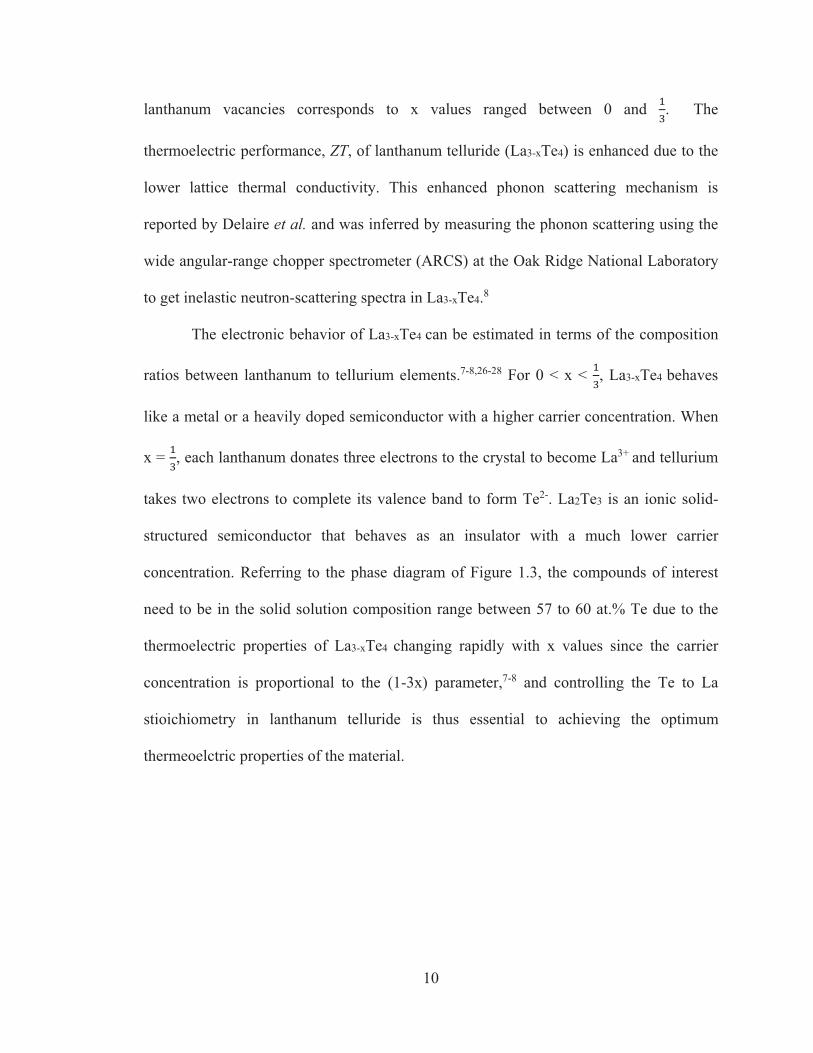
The electronic behavior of La3-xTe4 can be estimated in terms of the composition
ratios between lanthanum to tellurium elements.7-8,26-28 For 0 < x < ��, La3-xTe4 behaves
like a metal or a heavily doped semiconductor with a higher carrier concentration. When
x = ��, each lanthanum donates three electrons to the crystal to become La3+ and tellurium
takes two electrons to complete its valence band to form Te2-. La2Te3 is an ionic solid-
structured semiconductor that behaves as an insulator with a much lower carrier
concentration. Referring to the phase diagram of Figure 1.3, the compounds of interest
need to be in the solid solution composition range between 57 to 60 at.% Te due to the
thermoelectric properties of La3-xTe4 changing rapidly with x values since the carrier
concentration is proportional to the (1-3x) parameter,7-8 and controlling the Te to La
stioichiometry in lanthanum telluride is thus essential to achieving the optimum
thermeoelctric properties of the material.
11
Figure 1.3 Lanthanum-Tellurium phase diagram.42 The green arrow indicates the solid solution of La3-xTe4 at 57-60 at. % of Te and the red arrow points to the solidus line of La2Te3. The phase diagram reprinted from ASM Alloy Phase Diagrams Center. Copyright 2006, ASM International.
12
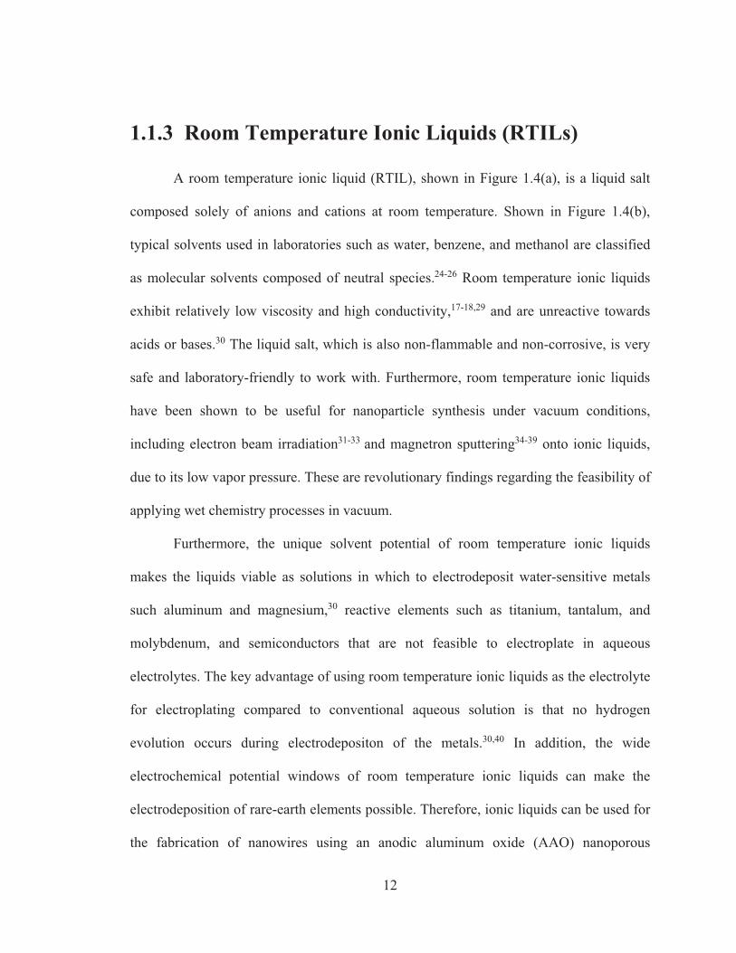
1.1.3 Room Temperature Ionic Liquids (RTILs)
A room temperature ionic liquid (RTIL), shown in Figure 1.4(a), is a liquid salt
composed solely of anions and cations at room temperature. Shown in Figure 1.4(b),
typical solvents used in laboratories such as water, benzene, and methanol are classified
as molecular solvents composed of neutral species.24-26 Room temperature ionic liquids
exhibit relatively low viscosity and high conductivity,17-18,29 and are unreactive towards
acids or bases.30 The liquid salt, which is also non-flammable and non-corrosive, is very
safe and laboratory-friendly to work with. Furthermore, room temperature ionic liquids
have been shown to be useful for nanoparticle synthesis under vacuum conditions,
including electron beam irradiation31-33 and magnetron sputtering34-39 onto ionic liquids,
due to its low vapor pressure. These are revolutionary findings regarding the feasibility of
applying wet chemistry processes in vacuum.
Furthermore, the unique solvent potential of room temperature ionic liquids
makes the liquids viable as solutions in which to electrodeposit water-sensitive metals
such aluminum and magnesium,30 reactive elements such as titanium, tantalum, and
molybdenum, and semiconductors that are not feasible to electroplate in aqueous
electrolytes. The key advantage of using room temperature ionic liquids as the electrolyte
for electroplating compared to conventional aqueous solution is that no hydrogen
evolution occurs during electrodepositon of the metals.30,40 In addition, the wide
electrochemical potential windows of room temperature ionic liquids can make the
electrodeposition of rare-earth elements possible. Therefore, ionic liquids can be used for
the fabrication of nanowires using an anodic aluminum oxide (AAO) nanoporous
13
template-assisted method. Some have even suggested that cation and anion effects from
room temperature ionic liquids may influence the morphology and crystal size of
deposits.30,41
Figure 1.4 (a) Schematic of room temperature ionic liquids composed solely by anions and cations. (b) Schematic of molecular structure of typical molecular solvents such as benzene and water.
14
1.2 Experimental
This section is an adapted reproduction from Mater. Res. Soc. Symp. Proc. Vol. 1543
(2013). Copyright 2013, Materials Research Society.
Tellurium powder (Aldrich Chemistry, 99.8%) was dissolved in concentrated
nitric acid to form the oxide cations, (HTeO2)+, at room temperature until no further
reaction occurred. A tellurium seed layer (~100 nm thick) was then electrodeposited onto
a nickel or silver substrate (cleaned and etched with HNO3 : deionized water = 1 : 3) in a
three-electrode electrochemical system designed in-house. A nickel or silver substrate
served as the working electrode in the experiment. A platinum mesh was used as the
counter-electrode and an Ag/AgCl electrode was used as the reference electrode. The
electrolyte contained 0.025M (HTeO2)+ in 3M HNO3. Potentiastatic deposition was
performed at -0.3V vs. Ag/AgCl reference electrode at room temperature.
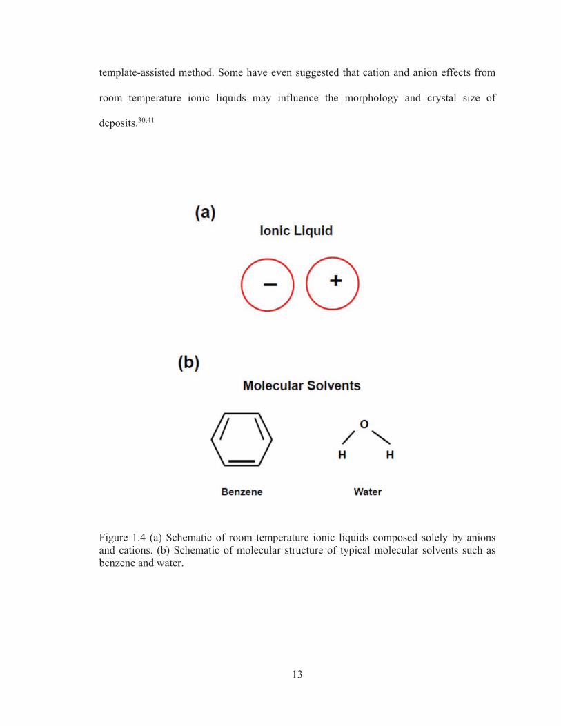
The ionic liquid, 1-ethyl-3-methylimidazolium bromide (EMIB) (molecular
structure is shown in Figure 1.5(b)), was prepared by first stirring 100 ml of 1-
methylimidazole (Alfa Aesar, 99%) (molecular structure is shown in Figure 1.5(a)) in a
beaker at 70°C followed by slowly adding 300 ml of bromoethane (Sigma-Aldrich,
reagent grade, 98%, CH3CH2Br) into the beaker. The solution was then allowed to stir
about 24 hours at 70°C. Ethyl ether (Fisher Scientific, anhydrous and certified ACS) was
added to extract and wash the liquid. The ionic liquid was then stirred at 70°C for 5 hours
to burn off any volatiles left in the solution.
15
Figure 1.5 Molecular structure of (a) 1-methylimidazole and (b) the anions and cations used as the RTIL solvents in the study.
Lanthanum telluride films were electrodeposited onto the tellurium seed layer in a
three-electrode electrochemical system. The nickel or silver substrate served as the
working electrode in the experiment. A platinum mesh was used as the counter electrode
and an Ag/AgCl electrode was used as the reference electrode. The electrolyte contained
0.9g of lanthanum nitrate hydrate (Aldrich Chemistry, 99.9%) dissolved in 10 ml of 1-
ethyl-3-methylimidazolium bromide (EMIB) ionic liquid and a few ml of 0.025M
(HTeO2)+ depending on the La-Te stioichiometric ratio of the desired product as shown
in Table 1. The potentiastatic deposition was performed at a range from -1.2 to -1.5V vs.
Ag/AgCl reference electrode at room temperature. Ar gas was bubbled into the
(a)
(b)
16
electrolyte to remove oxygen from the solution throughout the experiment. A typical
deposition duration was about 2 hours and the resulting film thickness was about 1 �m as
measured by a profilometer. The deposited films were then rinsed with ethanol and
deionized water, followed by storing in vacuum. The morphology of the samples was
investigated using a field emission scanning electron microscope (JEOL JSM-6700F)
equipped with an energy dispersive x-ray spectrometer (EDAX) for composition analysis.
X-ray diffraction patterns of the deposited samples were obtained using a Philips X’Pert
X-ray Diffractometer (XRD).
Table 1.1 Electrodeposition Conditions of La and La-Te Alloys.
Table reprinted from Mater. Res. Soc. Symp. Proc. Vol. 1543 (2013). Copyright 2013, Materials Research Society.
Counter Electrode
Working Electrode
Electrolyte (in 10 ml ionic liquid)
Deposition Voltage (vs. Ag/AgCl
Reference Electrode)
Product
Pt Ag 0.9g La(NO3)3·6H2O -1.5V La
Pt Ag 0.2 ml [0.025M (HTeO2)+]
+ 0.9g La(NO3)3·6H2O -1.5V LaTe
Pt Ag 0.3 ml [0.025M (HTeO2)+]
+ 0.9g La(NO3)3·6H2O -1.5V La3-xTe4
Pt Ag 0.2 ml [0.025M (HTeO2)+]
+ 0.9g La(NO3)3·6H2O -1.2V La2Te3
Pt Ag 1 ml [0.025M (HTeO2)+] +
0.9g La(NO3)3·6H2O -1.2V LaTe2
Pt Ag 0.5 ml [0.025M (HTeO2)+]
+ 0.9g La(NO3)3·6H2O -1.5V LaTe3
17
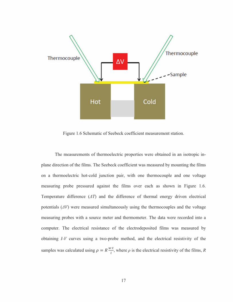
Figure 1.6 Schematic of Seebeck coefficient measurement station.
The measurements of thermoelectric properties were obtained in an isotropic in-
plane direction of the films. The Seebeck coefficient was measured by mounting the films
on a thermoelectric hot-cold junction pair, with one thermocouple and one voltage
measuring probe pressured against the films over each as shown in Figure 1.6.
Temperature difference (�T) and the difference of thermal energy driven electrical
potentials (�V) were measured simultaneously using the thermocouples and the voltage
measuring probes with a source meter and thermometer. The data were recorded into a
computer. The electrical resistance of the electrodeposited films was measured by
obtaining I-V curves using a two-probe method, and the electrical resistivity of the
samples was calculated using % � & '()* , where � is the electrical resistivity of the films, R
18
is the electrical resistance of the films, w is the width of the probe tips, t is the thickness
of the films, and l is the distance between the two measuring probes in the measurement.
1.3 Results and Discussion
A tellurium thin film was firstly electrodeposited as the seed layer to minimize the
lattice mismatch between the substrate and the deposit to reduce defect formation. The
thickness of the lanthanum telluride deposited films was about 1 �m. Since it was
essential to synthesize precise stiochiometries of the compound, trials were conducted
based on the reduction potentials of each element. The ratio of concentration of each
element dissolved in the ionic liquid was varied. The morphologies and chemical
compositions of the deposited films were characterized using scanning electron
microscopy (SEM), XRD, and EDAX analysis after each deposition. It was critical to
determine the correct deposition potentials and solution concentration to control the Te to
La ratio.
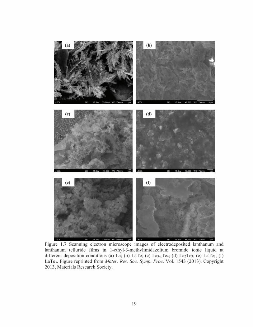
19
Figure 1.7 Scanning electron microscope images of electrodeposited lanthanum and lanthanum telluride films in 1-ethyl-3-methylimidazolium bromide ionic liquid at different deposition conditions (a) La; (b) LaTe; (c) La3-xTe4; (d) La2Te3; (e) LaTe2; (f) LaTe3. Figure reprinted from Mater. Res. Soc. Symp. Proc. Vol. 1543 (2013). Copyright 2013, Materials Research Society.
(a) (b)
(c) (d)
(e) (f)
20
Scanning electron microscope images of electrodeposited films displayed many
interesting surface structures as shown in Figure 1.7. Needle-like structures were
observed on the electrodeposited La films as shown in Figure 1.7(a). In Figure 1.7(b), the
homogenous crystalline LaTe domains with rough surface features covered the entire
substrate. On the other hand, it is noted that there were many nanostructured surface
features in the La3-xTe4 film as shown in Figure 1.7(c). The nanocrystalline features have
many grain boundaries in the microstructure that can scatter phonons more effectively
and may result in an enhanced figure of merit (ZT) due to lower thermal conductivity
associated with such nanostructured materials.
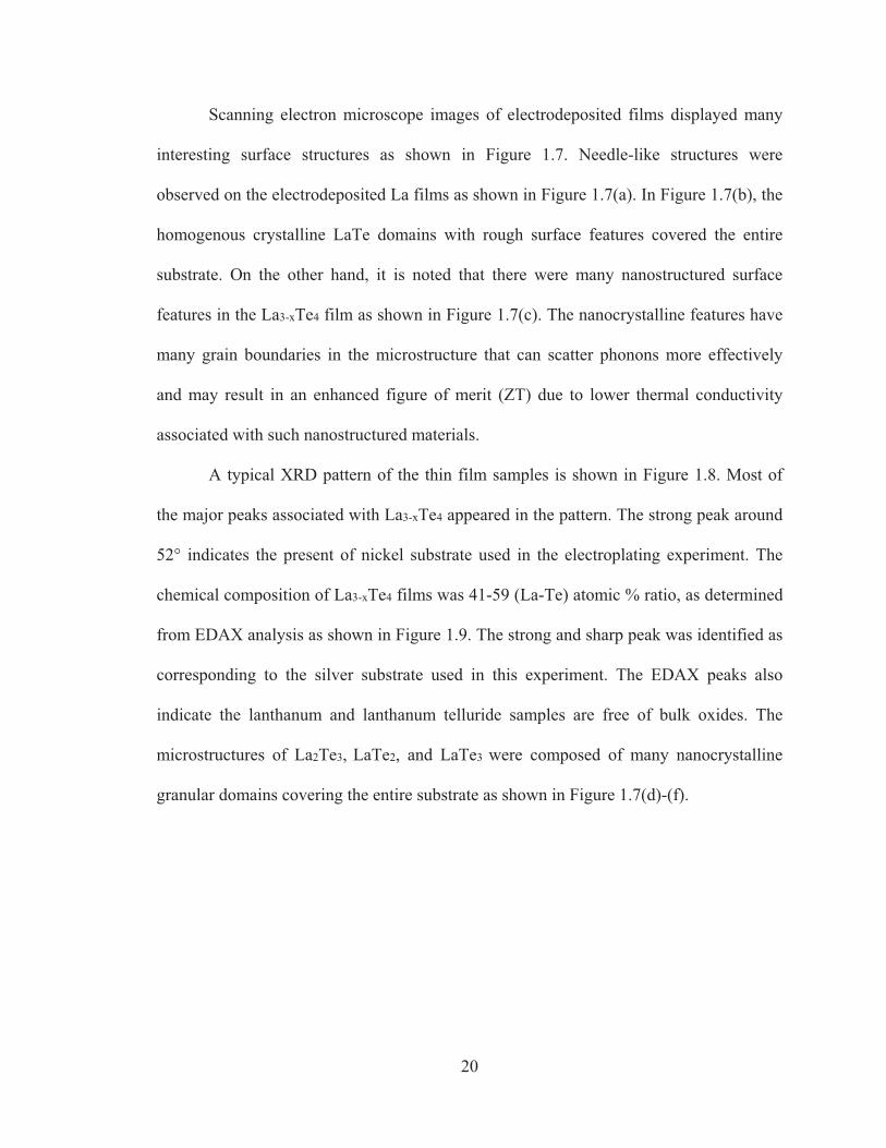
A typical XRD pattern of the thin film samples is shown in Figure 1.8. Most of
the major peaks associated with La3-xTe4 appeared in the pattern. The strong peak around
52° indicates the present of nickel substrate used in the electroplating experiment. The
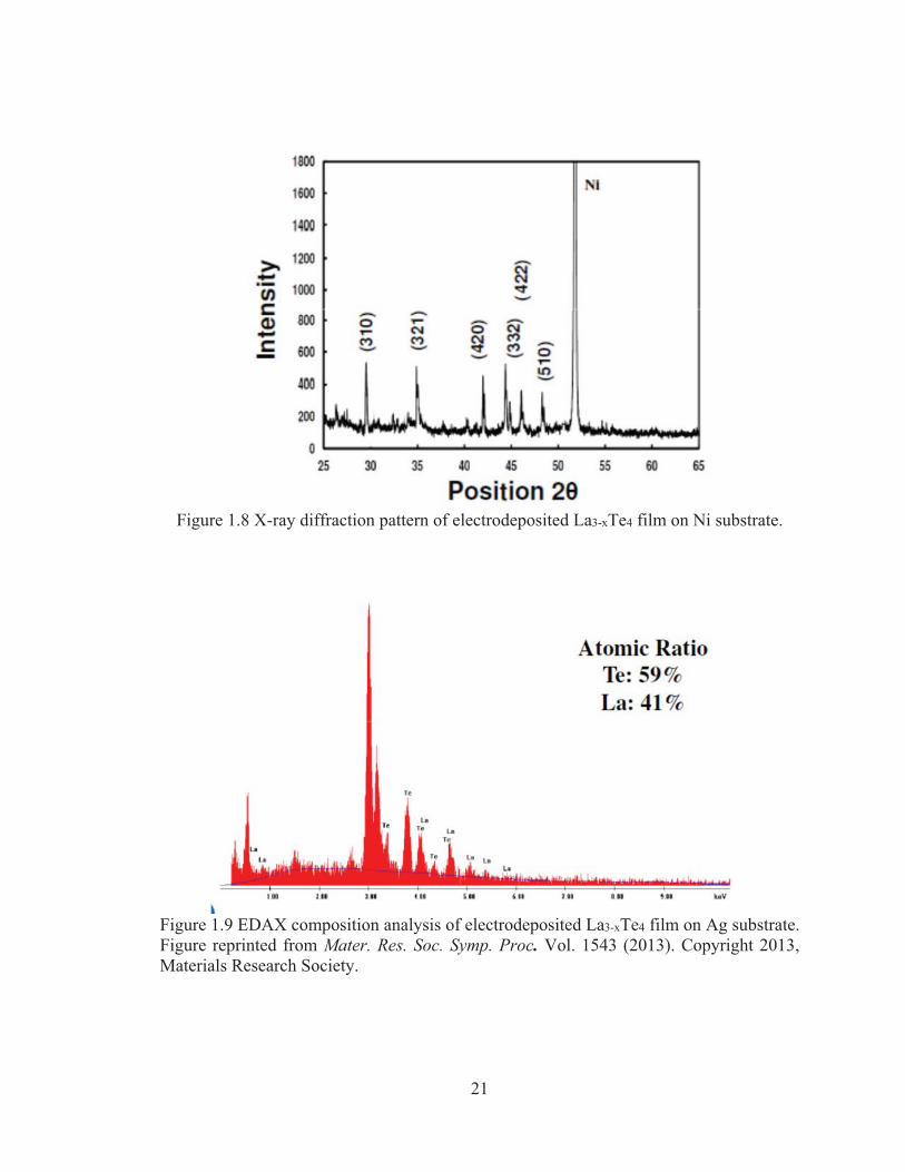
chemical composition of La3-xTe4 films was 41-59 (La-Te) atomic % ratio, as determined
from EDAX analysis as shown in Figure 1.9. The strong and sharp peak was identified as
corresponding to the silver substrate used in this experiment. The EDAX peaks also
indicate the lanthanum and lanthanum telluride samples are free of bulk oxides. The
microstructures of La2Te3, LaTe2, and LaTe3 were composed of many nanocrystalline
granular domains covering the entire substrate as shown in Figure 1.7(d)-(f).
21
Figure 1.8 X-ray diffraction pattern of electrodeposited La3-xTe4 film on Ni substrate.
Figure 1.9 EDAX composition analysis of electrodeposited La3-xTe4 film on Ag substrate. Figure reprinted from Mater. Res. Soc. Symp. Proc. Vol. 1543 (2013). Copyright 2013, Materials Research Society.
22
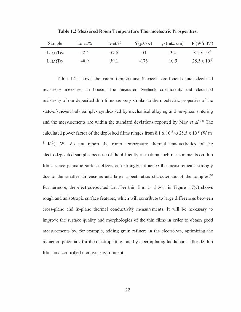
Table 1.2 Measured Room Temperature Thermoelectric Prosperities.
Sample La at.% Te at.% S (�V/K) � (m�-cm) P (W/mK2)
La2.82Te4 42.4 57.6 -51 3.2 8.1 x 10⁻⁵
La2.72Te4 40.9 59.1 -173 10.5 28.5 x 10⁻⁵
Table 1.2 shows the room temperature Seebeck coefficients and electrical
resistivity measured in house. The measured Seebeck coefficients and electrical
resistivity of our deposited thin films are very similar to thermoelectric properties of the
state-of-the-art bulk samples synthesized by mechanical alloying and hot-press sintering
and the measurements are within the standard deviations reported by May et al.7-8 The
calculated power factor of the deposited films ranges from 8.1 x 10⁻⁵ to 28.5 x 10⁻⁵ (W m-
1 K-2). We do not report the room temperature thermal conductivities of the
electrodeposited samples because of the difficulty in making such measurements on thin
films, since parasitic surface effects can strongly influence the measurements strongly
due to the smaller dimensions and large aspect ratios characteristic of the samples.20
Furthermore, the electrodeposited La3-xTe4 thin film as shown in Figure 1.7(c) shows
rough and anisotropic surface features, which will contribute to large differences between
cross-plane and in-plane thermal conductivity measurements. It will be necessary to
improve the surface quality and morphologies of the thin films in order to obtain good
measurements by, for example, adding grain refiners in the electrolyte, optimizing the
reduction potentials for the electroplating, and by electroplating lanthanum telluride thin
films in a controlled inert gas environment.

23
1.4 Conclusions
The feasibility of electrodepositing pure lanthanum and lanthanum telluride
compounds in ambient conditions has been demonstrated. Scanning electron microscope
images show that surface morphologies of the deposited films varied from needle-like to
granular structures depending on the deposition conditions. Such nanostructured surface
features on the electrodeposited samples may be responsible for enhancing ZT because
high density of grain boundaries may scatter phonons more effectively resulting in a
lowering of the thermal conductivity. The measured Seebeck coefficients and electrical
resistivity of the electrodeposited thin films are close to the state-of-the-art thermoelectric
properties of bulk samples synthesized by mechanical alloying and the hot-press
sintering. The calculated power factor of the deposited films ranged from 8.1 x 10⁻⁵ to
28.5 x 10⁻⁵ (W m-1 K-2). X-ray diffraction (XRD) patterns and the energy dispersive x-ray
(EDAX) composition analysis of electrodeposited La3-xTe4 films indicated that the
samples were single phase materials.
1.5 Future Work
Given the promising behavior observed in this work, clearly the next step is to
produce materials for which thermal conductivity can be measured so that the value of
ZT can be obtained. The reproducibility of electrodeposited lanthanum telluride thin
films can be improved by synthesizing the material in a well-controlled inert gas
environment such as a glove box to prevent possible oxide formation during the
fabrication process. In addition, the electrodeposition parameters such as precise
24
reduction potential and concentration of deposit in electrolyte can be optimized. It is also
worth noting that the detail of mechanism of metal and alloy electrodeposition in ionic
liquid should be examined. It is also proposed that the reported electroplating technique
could be used to synthesize elemental lanthanum and lanthanum telluride nanowire arrays
by using conventional template methods with anodic aluminum oxide (AAO) nanoporous
membranes. These samples could be studied to investigate the prediction that such
reduced dimensional materials will display even lower lattice thermal conductivity due to
enhancement of phonon interface scattering introduced by quantum confinement.
25
Bibliography
1. J. W. Swart, editor, Solid State Circuits Technologies, ISBN 978-953-307-045-2,
pp. 462, INTECH, Croatia (2010).
URL: http://www.intechopen.com/download/get/type/pdfs/id/6497
2. A. K. Samal and T. Pradeep, Lanthanum Telluride Nanowires: Formation,
Doping, and Raman Studies, J. Phys. Chem. C. 114, 5871-5878 (2010).
3. J. C. Kopera, “Inside the Nickel Metal Hydride Battery,” Cobasys (2004).
URL: http://www.cobasys.com/pdf/tutorial/inside_nimh_battery_technology.pdf
4. S. Gorman, As hybrid cars gobble rare metals, shortage looms, © Thomson
Reuters 2011, Aug 31, 2009. URL: http://www.reuters.com/article/2009/08/31/us-
mining-toyota-idUSTRE57U02B20090831
5. P. Bäuerlein, C. Antonius, Jens L�ffler, and J�rg K�mpers, Progress in high-
power nickel-metal hydride batteries, J. of Power Sources. 176, 547-554 (2008).
6. “Lanthanum,” Chemicool Periodic Table, Chmicool.com, Oct. 17, 2012.
URL http://www.chemicool.com/elements/lanthanum.html.
7. A. May, J.-P. Fleurial, and G. J. Snyder, Thermoelectric performance of
lanthanum telluride produced via mechanical alloying, Phys. Rev. B 78, 125205
(2008).
8. O. Delaire, A. F. May, M. A. McGuire, W. D. Porter, M. S. Lucas, M. B. Stone,
D. L. Abernathy, V. A. Ravi, S. A. Firdosy, and G. J. Snyder, Phonon density of
states and heat capacity of La3-xTe4, Phys. Rev. B 80, 184302 (2009).
26
9. G. D. Badge, S. D. Sartale, and C. D. Lokhande, Spray pyrolysis deposition of
lanthanum telluride thin films and their characterizations, Mate. Chem. and Phys.
89, 402-405 (2005).
10. T. H. Ramsey, H. Steinfink, and E. J. Weiss, The Phase Equilibria and Crystal
Chemistry of the Rare Earth-Group VI Systems. IV. Lanthanum-Tellurium, Inorg.
Chem., 4(8), 1154-1157 (1965).
11. T. H. Ramsey, H. Steinfink, and E. J. Weiss, Some Thermoelectric Properties of
Polycrystalline Lanthanum Telluride, LaTe1.7 to LaTe2.0, J. Appl. Phys. 34, 2917
(1963).
12. G. Chen, M. S. Dresselhaus, G. Dresselhaus. J. P. Fleurial, and T. Caillat, Recent
development in thermoelectric materials. Int. Mater. Rev. 48, 45-66 (2003).
13. L. D. Hicks and M. S. Dresselhaus, Effect of quantum-well structures on the
thermoelectric figure of merit, Phys. Rev. B 47, 12727 (1993).
14. L. D. Hicks and M. S. Dresselhaus, Thermoelectric figure of merit of a one-
directional conductor, Phys. Rev. B 47, 16631 (1993).
15. M. S. Dresselhaus, G. Chen, M. Y. Tang, R. G. Yang, H. Lee, D. Z. Wang, Z. F.
Ren, J.-P. Fleurial, and P. Gogna, New directions for low-dimensional
thermoelectric materials, Adv. Mater. 19 (2007).
16. J.-P. Fleurial, A. Borshchevsky, M. A. Ryan, W. Phillips, E. Kolawa, T. Kacisch,
and R. Ewell, Proceedings of XVI International Conference on Thermoelectrics,
Dresden, Germany, p. 641, 1997.
17. M. J. Earle and K. R. Sedden, Ionic liquids: Green solvents for the future, Pure
Appl. Chem. 72 (7), 1391-1398 (2000).
27
18. Covalent Associates, Inc., Introduction to Ionic Liquids.
URL:http://www.covalentassociates.com/Introduction%20to%20Ionic%20Liquid
s.pdf
19. D. M. Rowe, editor, CRC Handbook of Thermoelectrics, CRC Press, Boca Raton,
FL (1995).
20. D. M. Rowe, editor, CRC Handbook of Thermoelectric: Macro to Nano, CRC
Press, Taylor & Francis Group, LLC, Boca Raton, FL (2006).
21. J. P. Fleurial, Thermoelectric power generation materials: technology and
application opportunities, JOM Vol. 16 issue 4: 79-85 (2009).
22. G. J. Snyder and E. S. Toberer, Complex Thermoelectric Materials, Nature
Materials 7, 105-114 (2008).
23. S. M. Kauzlarich, S. R. Brown, and G. J. Snyder, Zintl Phases for thermoelectric
devices, Dalton Trans. 2099-2107 (2007).
24. C. Uher, in Thermoelectric Materials Research I (ed. T. Tritt). 139-253,
Semiconductors and Semimetals Series 69, Elsevier (2001).
25. G. S. Nolas, J. Poon, and M. Kanatzids, Recent developments in bulk
thermoelectric materials, Mater. Res. Soc. Bull. 31, 199-205 (2006).
26. M. Cutler, J. Leavy, and R. Fitzpatrick, Electron transport in semimetallic cerium
sulfide, Phys. Rev. 133, A1143 (1964).
27. M. Cutler and J. Leavy, Electron transport in high-resistivity cerium sulfide, Phys.
Rev. 133, A1153 (1964).
28. T. H. Ramsey, H. Steinfink, and E. J. Weiss, Thermoelectric and Electrical
Measurements in the La-Te System, J. Appl. Phys. 36 (2), 548-553 (1965).

28
29. T. Tsuda, C. L. Hussey, and G. R. Stafford, Progress in Surface Finishing with
Lewis Acidic Room-Temperature Chloroaluminate Ionic Liquids, ECS Trans. 3
(35), 217-231 (2007).
30. M. Armand, F. Endres, D. R. MacFarlane, H. Ohno, and B. Scrosati, Ionic-liquid
materials for the electrochemical challenges of future, Nature Materials 8, 621-
629 (2009).
31. A. Imanishi, M. Tamura, and S. Kuwabata, Formation of Au nanoparticles in an
ionic liquid by electron beam irradiation, Chem. Commun. 13, 1775-1777 (2009).
32. T. Tsuda, S. Seino, and S. Kuwabata, Gold nanoparticles prepared with a room-
temperature ionic liquid-radiation irradiation method, Chem. Commun. 44, 6792-
6794 (2009a).
33. T. Tsuda, T. Sakamoto, T. Nose, S. Seino, A. Imanishi, T. Uematsu, and S.
Kuwabata, Irradiation-Induced Metal Nanoparticles in Room-Temperature Ionic
Liquid, ECS Trans. 33 (7), 543-554 (2010a).
34. Y. Hatakeyama, M. Okamoto, T. Torimoto, S. Kuwabata, and K. Nishikawa,
Small-Angle X-ray Scattering Study of Au Nanoparticles Dispersed in the Ionic
Liquids 1-Alkyl-3-methyllmidazolium Tetrafluoroborate, J. Phys. Chem. C 113,
3917-3922 (2009).
35. Y. Hatakeyama, S. Takahashi, and K. Nishikawa, Can Temperature Control the
Size of Au Nanoparticles Prepared in Ionic Liquids by the Sputter Deposition
Technique?, J. Phys. Chem. C 114, 11098-11102 (2010).
36. T. Kameyama, Y. Ohno, T. Kurimoto, K. Okazaki, T. Uematsu, and T. Torimoto,
Size control and immobilization of gold nanoparticles stabilized in an ionic liquid
29
on glass substrates for plasmonic applications, Phys. Chem. Chem. Phys. 12,
1804-1811 (2010).
37. T. Suzuki, K. Okazaki, T. Kiyama, S. Kuwabata, and T. Torimoto, A Facile
Synthesis of AuAg Alloy Nanoparticles Using a Chemical Reaction Induced by
Sputter Deposition of Metal onto Ionic Liquids, Electrochemistry 77, 636-638
(2009).
38. T. Tsuda and C. L. Hussey, Electrochemistry of room temperature ionic liquids
and melts, R. E. White (ed.) Modern Aspects of Electrochemistry Vol. 45,
Springer Science + Business Media, New York, pp. 63-174 (2009).
39. T. Tsuda, K. Yoshii, T. Torimoto, and S. Kuwabata, Oxygen reducation catalytic
ability of platinum nanoparticles prepared by room-temperature ionic liquid-
sputtering method, J. Power Sources 195, 5980-5985 (2010b).
40. S. Legeai, S. Diliberto, N. Stein, C. Boulanger, J. Estager, N. Papaiconomou, and
M. Draye, Room-temperature ionic liquid fro lanthanum electrodepsoition, Elec.
Comm. 10, 1661-1664 (2008).
41. A. P. Abbott and K. J. McKenzie, Application of ionic liquids to the
electrodeposition of metals, Phys. Chem. Chem. Phys. 8, 4265-4279 (2006).
42. H. Okamoto, La-Te (Lanthanum-Tellurium), Binary Alloy Phase Diagrams, II
Ed., Ed. T. B. Massalski, Vol.3, 1990, p 2430-2431. ASM Alloy Phase Diagrams
Center, P. Villars, editor-in-chief; H. Okamoto and K. Cenzual, section editors;
ASM International, Materials Park, OH, USA, 2006-2013.
URL: http://www1.asminternational.org/asmenterprise/APD/PrintViewAPD.aspx
30
Chapter 2
Synthesis and Characterization of Vertically-
Aligned Gold Nanowire Arrays
Ferromagnetic Composite Films
2.1 Introduction
Ordered nanocomposite structures have attracted significant interest as their
unique electrical and optical properties can lead to localized surface plasmon resonance
(LSPR). This behavior has to potential to improve current commercial lab-on-a-chip
surface enhanced Raman scattering (SERS) technologies such as portable Raman
systems, used to detect and identify chemical and biological agents and explosive
compounds at trace levels.1 LSPR describes a resonance phenomenon of surface electron
density in metallic nanoscale structures where the characteristic length scale of the
material is smaller than the wavelength of incident light.2 LSPR signaling enhancement
depends on the type of the material (gold, silver, and platinum), and the size, shape, and
spacing of nanostructured materials.3-6 For gold, LSPR leads to strong plasmon
absorption in the visible wavelength regime.3 Highly ordered gold nanowire arrays can
sustain large electromagnetic fields at a high density of sites within the structure upon the
31
excitation of light.4-6 This structure becomes an excellent substrate for LSPR
enhancement.
However, other than gold, silver, and platinum, there are still many classes of
materials that have plasmon resonance and other interesting optical-electronic properties.
It has been known that ferromagnetic materials such as nickel or cobalt having a spectral
position of the plasmon resonance similar to that of silver.6 Therefore, the combination of
the ferromagnetic resonance with plasmonic resonance may lead to a novel material for
LSPR signaling enhancement.6-7 Here we report on the fabrication and characterization of
vertically-aligned gold nanowire arrays in ferromagnetic matrices (nickel and iron). It is
thought that the magnetic response of the ferromagnetic matrices may couple with the
plasmonic behavior, thus amplifying the LSPR response. Our goal in this work is to
synthesize large area, reproducible, and homogeneous substrates that may have
applications as LSPR materials for biological and chemical sensors.
2.1.1 Localized Surface Plasmon Resonance (LSPR)
The free electrons in noble metals are free to travel through the material. The
mean free path due to phonon scattering in bulk gold and silver is ~ 50 nm. In
nanostructured materials smaller than this mean free path, the electron scattering is
expected to be dominated by scattering at the surfaces.8 Localized surface plasmon
resonance (LSPR) describes a induced resonance phenomenon of surface free electron
waves in noble metallic nanostructures such as nanoparticles, nanoscale rough surface,
and nanowires, where the characteristic length scale of the materials is smaller than the
wavelength of incident light.2,9-10 This resonance is a coherent collective oscillation of the
32
surface electrons in the conduction band excited and polarized by the incident light
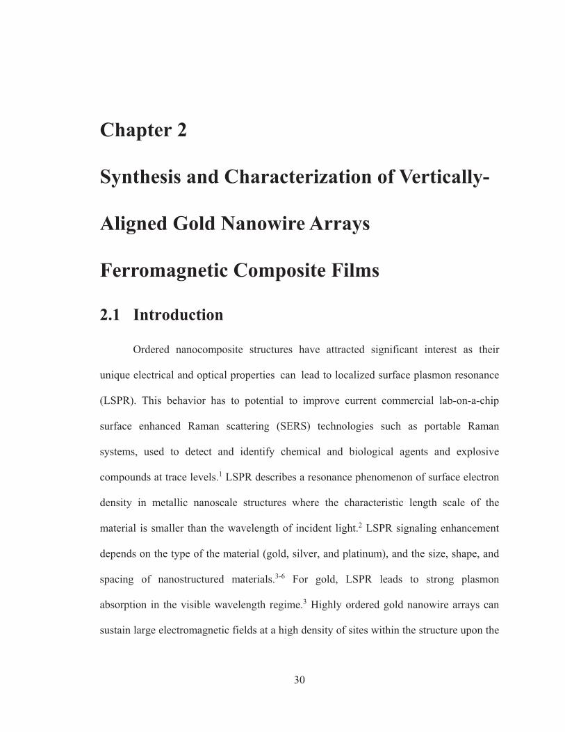
(electromagnetic wave).5,7 As shown in Figure 2.1, an incident light interacts with
nanoparticles that are much smaller in size than the wavelength of that incident light.
This condition leads to a plasmon that oscillates locally around the particles (localized
surface plasmon resonance) with a frequency which matches the frequency of the
incident light. The resonance causes a collective oscillation of the conduction electrons in
the metal nanoparticles.11
Figure 2.1 Schematic of a localized surface plasmon for a sphere, showing the displacement of the conduction electron charge could relative to the nuclei. Figure reprinted from Annu. Rev. Phys. Chem. 58, 267-297 (2007). Copyright 2007, Annual Reviews.
Since the LSPR occurs at the surface, as the size or the shape of the nanoparticles
change, the surface geometry also changes, resulting in a shift in the electromagnetic
field on the surface. This causes a change in the frequency of collective oscillation of the
conduction electrons, generating different cross-sections for LSPR respondence.15
Furthermore, if the dielectric constant of the surrounding material of the nanoparticles
changes, this will have an effect on the oscillation frequency of the surface electrons due
33
to the varying ability of the surface to accommodate electron charge density from the
nanoparticles.12 Therefore, the frequency and intensity of LSPR highly depend on the
type of the material (gold, silver, or platinum), the size, the shape, the interspacing, and
the dielectric constant of nanoparticles and their surrounding materials.3-6,8,11-13
Based on the development of modern methods extending from the Mie solution to
Maxwell’s equations describing the surface plasmon resonance for a small sphere
interacting with an electromagnetic field which can be used to calculate the surface
plasmon resonance for arbitrary geometries.12 Gold nanorods (nanowires) have generated
interest as materials to study LSPR because an increase in the aspect ratio of gold
nanorods contributes to the enhancement of the intensity and the longitudinal plasmon
resonance, resulting in an enhancement of the electromagnetic field.12,14 Therefore,
highly ordered gold nanowire arrays can sustain larger electromagnetic fields at a high
density of sites within the structure upon the excitation and polarization of incident
light.4-6 As a result, vertically-aligned gold nanowire arrays may prove to be excellent
substrates for LSPR enhancement.
Nobel metals such as gold, silver, or platinum are common materials for
determining LSPR effect because their energy levels of d-d transitions exhibited LSPR
are in the visible range of the spectrum.8,12 As a result, the wavelengths of the incident
light that cause this collective oscillation conduction electrons are selectively absorbed by
nanostructured materials and can be measured using ultraviolet-visible (UV-Vis)
spectropscopy.5,11 Also, the formation of enhanced electromagnetic fields that extend
from the metal nanostructured surfaces is responsible for the enhancement observed in
surface-enhanced Raman scattering (SERS).7,9,11 Therefore, not only is LSPR a powerful
34
technique for chemical and biological sensing, but also is responsible for the
electromagnetic field enhancements that leads to surface-enhanced Raman scattering
(SERS).7,9 With the some understandings of LSPR effect, the purpose of this work is to
develop a synthesis method for large area, reproducible, and homogeneous samples that
may have applications for localized surface plasmon resonance effects.
2.2 Experimental
Vertically-aligned gold nanowires grown on a gold substrate were fabricated by
electrodeposition. Anodic aluminum oxide (AAO) nanoporous membranes (Whatman,
porosity: 40%, pore spacing: ~ 140 nm, membrane thickness: ~ 60 �m) which were about
60 �m thick and had pore size about 100 nm were used as templates in these experiments.
A gold film about 1 �m thick was electron beam evaporated onto the back side of the
AAO membrane and served as the working electrode. A platinum mesh was used as the
counter electrode and an Ag/AgCl electrode was used as the reference electrode in the
three-electrode electrochemical system designed in house. The electrolyte was gold
plating solution (Alfa Aesar, electroless, metal content � 3.7 g/L). Potentiastatic
deposition was run at -1 V vs. Ag/AgCl reference electrode at room temperature for 1
hour. Gold ions in the electrolyte are restricted to only be reduced into elemental gold
inside the nanopores. The AAO template was then dissolved in a 4 M aqueous sodium
hydroxide (NaOH) solution at room temperature for 2 hours. The exposed gold
nanowires on the substrate were subsequently thoroughly rinsed with DI water.
Vertically standing gold micropilliars grown on a gold substrate were fabricated
by a similar electrodeposition process as described above. Polycarbonate membranes
35
(Whatman®) which are about 12 �m thick and have pore size about 5 �m were used as
templates in these experiments. A copper film about 1 �m thick was electron beam
evaporated onto the back side of the AAO membrane and served as the working
electrode. A platinum mesh was used as the counter electrode and an Ag/AgCl electrode
was used as the reference electrode in the three-electrode electrochemical system
designed in house. The electrolyte was gold plating solution (Alfa Aesar, electroless,
metal content � 3.7 g/L). Potentiastatic deposition was run at -1 V vs. Ag/AgCl reference
electrode at room temperature for 15 minutes. Gold ions in the electrolyte were restricted
to only being reduced into elemental gold inside the micropores. The polycarbonate
template was dissolved in dichloromethane (Sigma-Aldrich, anhydrous, � 99.8%) at
room temperature for 30 minutes and then the sample was ultrasonicated in the
suspension for 5 minutes. The gold microwires with the substrate were thoroughly rinsed
with deionized water.
After etching away the AAO nanoporous membrane, nickel was electron beam
evaporated at a deposition rate of approximately 1 Å/s onto the exposed gold nanowires
resulting in a nanocomposite composed of a nickel matrix with embedded gold
nanowires. Another set of nickel matrix nanocomposites were synthesized by
electrodepositing the nickel onto the gold nanowires using the same three-electrode
electrochemical system discussed previously. The electrodeposition was carried out at a
constant current density of 1 mA/cm2 at room temperature for 2 hours. The counter
electrode and reference electrode used in the experiment were nickel foils (Alfa Aesar,
99.95%, 0.25 mm thick). The electrolyte used in the electrochemical process was a 1.24
M nickel sulfate hexahydrate (Sigma Aldrich, ACS reagent, 99%, 227676-500G), 0.5 M
36
boric acid (Alfa Aesar, 99.99%, metal basis, CAS#10043-35-3), 0.02 M NiCl2 (Sigma
Aldrich, 98%, 339350-250G), 0.5 g/L sodium dodecyl sulfate (SDS) (Sigma Aldrich, for
molecular biology, L4390-100G), and 0.1 g/L coumarin 6 (Sigma Aldrich, 98%, 442631-
5G) aqueous solution.
Samples with iron matrices were fabricated by electrodepositing the iron onto the
gold nanowires from an aqueous solution of 1 M iron sulfate hephahydrate (Sigma
Alrich, plant cell culture tested, +,--./, 0.43 M H4ClN (Sigma Aldrich, for molecular
biology, + 99.5%, A9434-500G), 0.3 M NaCl (Sigma Aldrich, BioXtra, + 99.5%,
S7653-1KG), 15 g/L L-asccorbic acid (Alfa Aesar, 99+%, CAS#50-81-7), 1 g/L
saccharin (Sigma Aldrich, 98+%, 109185-500G) and 1 g/L sodium dodecyl sulfate (SDS)
(Sigma Aldrich, for molecular biology, L4390-100G). The electrochemical deposition
was carried out for 2 hours at a constant current density of 1.5 mA/cm2 at room
temperature. A platinum mesh was used as the counter electrode and an Ag/AgCl
electrode as the reference electrode. The morphology of the samples was investigated
using a JEOL JSM-6700F field emission scanning electron microscope (SEM). The
chemical composition of the deposited films was characterized using energy dispersive x-
ray (EDAX) analysis.
2.3 Results and Discussion
The anodic aluminum oxide (AAO) nanoporous membrane as shown in Figure
2.2 used in this work exhibited a hexagonally arranged nanoporous arrays with pore
diameter and pore interspacing distance about 100 nm and 150 nm, respectively. Figure
2.3(a) and 2.2(b) show the top view and the side view, respectively of the scanning
37
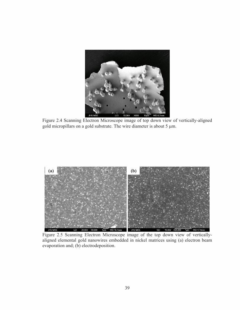
electron micrographs of vertically-aligned gold nanowire arrays on a gold substrate after
dissolution of the AAO template. It can be seen that the nanowire arrays were highly
dense and well attached to the gold substrate. The average diameter of gold nanowires
was about 100 nm, which is consistent with the pore size of the AAO template used in the
electrochemical deposition. The nanowires have initial lengths of approximately 500 to
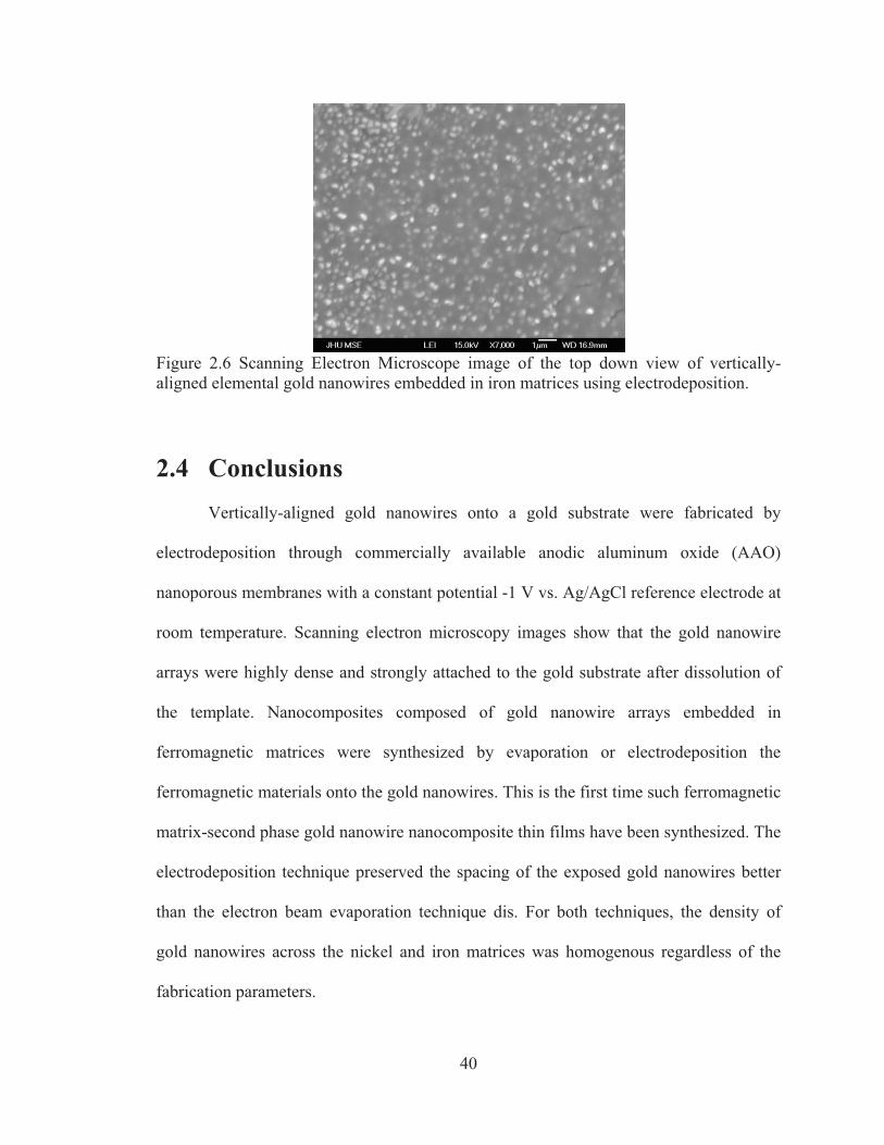
800 nm, corresponding to an aspect ratio of 5 to 8. Figure 2.4 show the vertically
standing Au micropillars grown on an Au substrate. These pillars are strongly attached to
the Au substrate.
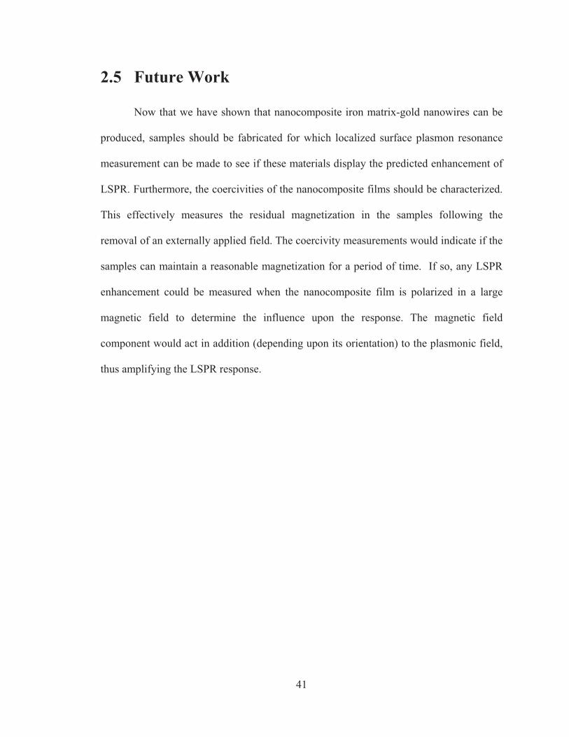
Figure 2.5(a) shows the SEM image of vertically-aligned gold nanowires (white
dots) embedded in nickel matrices (light gray areas) manufactured by electron beam
evaporating nickel onto the electrodeposited nanowire array. The interspacing of the
exposed gold nanowires ranged from a few hundreds of nanometers to a few
micrometers. Figure 2.5(b) shows the SEM image of vertically-aligned gold nanowires
(white dots) embedded in nickel matrices (light gray areas) manufactured by
electrodepositing nickel around the gold nanowire array. Comparing between Figure
2.5(a) to Figure 2.5(b), it is seen that the electrodeposition technique preserved the
spacing of the exposed gold nanowires better than the electron beam evaporation
technique did. In addition, the surface of the nickel matrix by electron beam evaporation
was rougher than that obtained by electrodeposition. Energy dispersive x-ray analysis
gave a composition of 98 atomic % of gold at the tips of the exposed gold nanowires
indicating minimal coating of the nickel by both electron beam evaporation and
electrodeposition. Figure 2.6 shows the SEM image of vertically-aligned gold nanowires
(white dots) embedded in iron matrices (gray areas) manufactured by electrodeposition of
38
iron onto the gold nanowire array. The spacing of the exposed gold nanowires ranged
from a few hundreds of nanometers to a few micrometers. For both techniques, the
density of gold nanowires across the nickel and iron matrices was homogenous regardless
of the fabrication parameters.
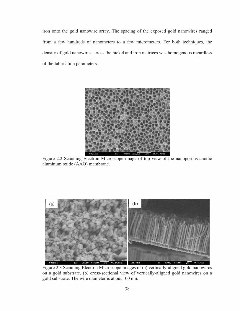
Figure 2.2 Scanning Electron Microscope image of top view of the nanoporous anodic aluminum oxide (AAO) membrane.
Figure 2.3 Scanning Electron Microscope images of (a) vertically-aligned gold nanowires on a gold substrate, (b) cross-sectional view of vertically-aligned gold nanowires on a gold substrate. The wire diameter is about 100 nm.
(a) (b)
39
Figure 2.4 Scanning Electron Microscope image of top down view of vertically-aligned gold micropillars on a gold substrate. The wire diameter is about 5 �m.
Figure 2.5 Scanning Electron Microscope image of the top down view of vertically-aligned elemental gold nanowires embedded in nickel matrices using (a) electron beam evaporation and; (b) electrodeposition.
(a) (b)
40
Figure 2.6 Scanning Electron Microscope image of the top down view of vertically-aligned elemental gold nanowires embedded in iron matrices using electrodeposition.
2.4 ConclusionsVertically-aligned gold nanowires onto a gold substrate were fabricated by
electrodeposition through commercially available anodic aluminum oxide (AAO)
nanoporous membranes with a constant potential -1 V vs. Ag/AgCl reference electrode at
room temperature. Scanning electron microscopy images show that the gold nanowire
arrays were highly dense and strongly attached to the gold substrate after dissolution of
the template. Nanocomposites composed of gold nanowire arrays embedded in
ferromagnetic matrices were synthesized by evaporation or electrodeposition the
ferromagnetic materials onto the gold nanowires. This is the first time such ferromagnetic
matrix-second phase gold nanowire nanocomposite thin films have been synthesized. The
electrodeposition technique preserved the spacing of the exposed gold nanowires better
than the electron beam evaporation technique dis. For both techniques, the density of
gold nanowires across the nickel and iron matrices was homogenous regardless of the
fabrication parameters.
41
2.5 Future Work
Now that we have shown that nanocomposite iron matrix-gold nanowires can be
produced, samples should be fabricated for which localized surface plasmon resonance
measurement can be made to see if these materials display the predicted enhancement of
LSPR. Furthermore, the coercivities of the nanocomposite films should be characterized.
This effectively measures the residual magnetization in the samples following the
removal of an externally applied field. The coercivity measurements would indicate if the
samples can maintain a reasonable magnetization for a period of time. If so, any LSPR
enhancement could be measured when the nanocomposite film is polarized in a large
magnetic field to determine the influence upon the response. The magnetic field
component would act in addition (depending upon its orientation) to the plasmonic field,
thus amplifying the LSPR response.
42
Bibliography
1. P. Daniel, NRL Scientists Elevate Warfighter Readiness against Invisible Threats
(2011).
URL: http://www.nrl.navy.mil/media/news-releases/2011/nrl-scientists-elevate-
warfighter-readiness-against-invisible-threats
2. K. Mitsui, Y. Handa, and K. Kajikawa, Optical fiber affinity biosensor based on
localized surface plasmon resonance, Appl. Phys. Lett. 85, 4231 (2004).
3. C. J. Murphy, A. M. Gole, S. E. Hunyadi, and C. J. Orendoff, One-Dimensional
Colloidal Gold and Silver Nanostructures, Inorg. Chem. 45, 7544-7554 (2006).
4. L. Billot, M. L. de la Chapelle, A. S. Grimault, A. Vial, D. Barchiesi, J.-L. Bijeon,
P.-M. Adam, and P. Royer, Surface enhanced Raman scattering on gold nanowire
arrays: evidence of strong multipolar surface plasmon resonance enhancement,
Chem. Phys. Lett. 422, 303-307 (2006).
5. H. M. Hiep et al., A Localized surface plasmon resonance based immunosensor
for the detection of casein in milk, Sci. Technol. Adv. Mater. 8 (4), 331-338
(2007).
6. G. Sauer, G. Brehm, S. Schneider, H. Graener, G. Seifert, K. Nielsch, J. Choi, P.
Göring, U. Gösele, P. Miclea, and R. B. Wehrspohn, Surface-enhanced Raman
spectroscopy employing monodisperse nickel nanowire arrays, Appl. Phys. Lett.
88, 023106 (2006).
7. K. A. Willets and R. P. Van Duyne, Localized Surface Plasmon Resonance
Spectroscopy and Sensing, Annu. Rev. Phys. Chem. 58, 267-297 (2007).
43
8. E. Petryayeva and U. Krull, Localized surface plasmon resonance:
Nanostructures, bioassays and biosensing – A review, Analytica Chimica Acta
706, 8-24 (2011).
9. A. J. Haes, S. Zou, G. C. Schatz, and R. P. Van Duyne, A Nanoscale Optical
Biosensor: The Long Range Distance Dependence of the Localized Surface
Plasma Resonance of Noble Metal Nanoparticles, J. Phys. Chem. B 108, 109-116
(2004).
10. S. Underwood and P. Mulvancy, Effect of the Solution Refractive Index on the
Color of Gold Colloids, Langmuir 10, 3427-3430 (1994).
11. A. J. Haes, S. Zou, J. Zhao, G. C. Schatz, and R. P. Van Duyne, Localized
Surface Plasmon Resonance Spectroscopy near Molecular Resonances, J. Am.
Chem. Soc. 128, 10905-10914 (2006).
12. S. Eustis and M. A. El-Sayed, Why gold nanoparticles are more precious than
pretty gold: Noble metal surface plasmon resonance and its enhancement of the
radiative and nonradiative properties of nanocrystals of different shapes, Chem.
Soc. Rev. 35, 209-217 (2006).
13. A. J. Haes, S. Zou, G. C. Schatz, and R. P. Van Duyne, Nanoscale Optical
Biosensor: Short Range Distance Dependence of the Localized Surface Plasma
Resonance of Noble Metal Nanoparticles, J. Phys. Chem. B 108, 6961-6968
(2004).
14. C. J. Murphy, T. K. Sau, A. M. Gole, C. J. Orendorff, J. Gao; L. Gou, S. E.
Hunyadi, T. Li, Anisotropic Metal Nanoparticles: Synthesis, Assembly, and
Optical Applications, J. Phys. Chem. B 109(29), 13857-13870 (2005).
44
Chapter 3
A Novel Approach to the Synthesis of
Nanochanneled Nickel Films
3. 1 Introduction
Nanoporous metallic membranes have attracted significant interest owing to their
wide range of technological applications including catalysis,1-3 sensing,1,4 microfluidic
flow control2, and surface enhanced Raman scattering,1,5-6 among others. The ability to
control the pore size and thickness of nanoporous metallic films can optimize the
catalytic effects of fuel cells.1-2 In this case, conversions depend on kinetics or mass
transport rather than diffusion.1 Ultrathin (about 100 nm thick) nanoporous membranes
may overcome the limitation of high CO oxidation generation during the catalytic
reactions at the surface of a nanoporous metallic film.1 In addition, large pore size
membranes can be used to control microfluidic flow, while small pore size membranes
can be employed as sensor materials due to their high specific surface areas.2 However,
these membranes are very fragile and exhibit brittle fracture, which limit their possible
applications in flow through type catalysis.1,3,7
45
Nanoporous nickel films have attracted significant attention due to the high
electrochemically active surface area to volume ratio, resulting in structures that may
have extensive application in fuel cell and battery technologies.8-11 I report here on a
novel method to fabricate relatively thick (0.5 �m and larger) nanochanneled Ni
membranes by depositing nickel onto an anodic aluminum oxide (AAO) nanporous
substrates with vertically aligned nanochannels. For nickel membrane thickness of about
0.7 �m or smaller, the as-deposited material is nanoporous, with the nanopores in the
form of nanochannels aligned with those of the substrate. For thicker membranes, the as-
deposited nickel becomes continuous, and a template-guided electrochemical etching
technique12 was used to produce the nanochannels. This physical vapor deposition
followed by electrochemical etching approach represents a relatively simple
manufacturing method for producing high quality nanoporous metallic membranes for
technological applications. It is noted that there have been some reports on the fabrication
of nanoporous replicated films using polymethyl methacrylate (PMMA) as the replication
medium injected into the nanopores of an anodic aluminum oxide (AAO) membrane
under vacuum conditions.14-17 The disadvantages of this replication method are the
incompletion of the replication of the nanoporous features of AAO membranes and the
difficulty of injecting the replication medium under vacuum, resulting in the obstacles for
applying this method to industrial manufacturing processes. The approach reported here
of overlayer deposition onto a nanoporous substrate, followed by electrochemical etching
through the substrate to produce a thick metallic nanoporous metallic membrane,
represents a simple and robust manufacturing process that can be more easily scaled-up
for industrial purposes compared to other fabrication methods.
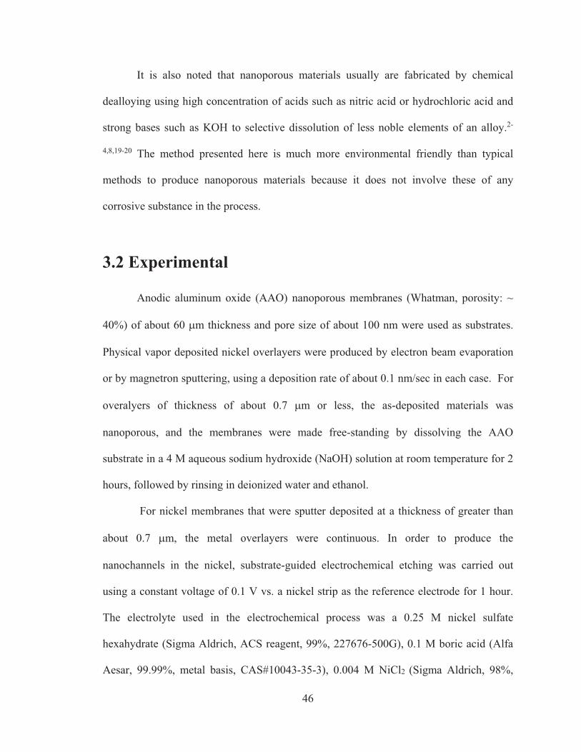
46
It is also noted that nanoporous materials usually are fabricated by chemical
dealloying using high concentration of acids such as nitric acid or hydrochloric acid and
strong bases such as KOH to selective dissolution of less noble elements of an alloy.2-
4,8,19-20 The method presented here is much more environmental friendly than typical
methods to produce nanoporous materials because it does not involve these of any
corrosive substance in the process.
3.2 Experimental
Anodic aluminum oxide (AAO) nanoporous membranes (Whatman, porosity: ~
40%) of about 60 �m thickness and pore size of about 100 nm were used as substrates.
Physical vapor deposited nickel overlayers were produced by electron beam evaporation
or by magnetron sputtering, using a deposition rate of about 0.1 nm/sec in each case. For
overalyers of thickness of about 0.7 �m or less, the as-deposited materials was
nanoporous, and the membranes were made free-standing by dissolving the AAO
substrate in a 4 M aqueous sodium hydroxide (NaOH) solution at room temperature for 2
hours, followed by rinsing in deionized water and ethanol.
For nickel membranes that were sputter deposited at a thickness of greater than
about 0.7 �m, the metal overlayers were continuous. In order to produce the
nanochannels in the nickel, substrate-guided electrochemical etching was carried out
using a constant voltage of 0.1 V vs. a nickel strip as the reference electrode for 1 hour.
The electrolyte used in the electrochemical process was a 0.25 M nickel sulfate
hexahydrate (Sigma Aldrich, ACS reagent, 99%, 227676-500G), 0.1 M boric acid (Alfa
Aesar, 99.99%, metal basis, CAS#10043-35-3), 0.004 M NiCl2 (Sigma Aldrich, 98%,
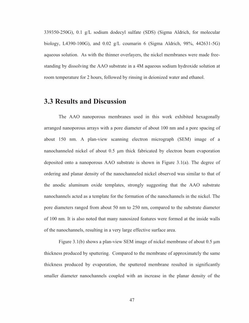
47
339350-250G), 0.1 g/L sodium dodecyl sulfate (SDS) (Sigma Aldrich, for molecular
biology, L4390-100G), and 0.02 g/L coumarin 6 (Sigma Aldrich, 98%, 442631-5G)
aqueous solution. As with the thinner overlayers, the nickel membranes were made free-
standing by dissolving the AAO substrate in a 4M aqueous sodium hydroxide solution at
room temperature for 2 hours, followed by rinsing in deionized water and ethanol.
3.3 Results and Discussion
The AAO nanoporous membranes used in this work exhibited hexagonally
arranged nanoporous arrays with a pore diameter of about 100 nm and a pore spacing of
about 150 nm. A plan-view scanning electron micrograph (SEM) image of a
nanochanneled nickel of about 0.5 �m thick fabricated by electron beam evaporation
deposited onto a nanoporous AAO substrate is shown in Figure 3.1(a). The degree of
ordering and planar density of the nanochanneled nickel observed was similar to that of
the anodic aluminum oxide templates, strongly suggesting that the AAO substrate
nanochannels acted as a template for the formation of the nanochannels in the nickel. The
pore diameters ranged from about 50 nm to 250 nm, compared to the substrate diameter
of 100 nm. It is also noted that many nanosized features were formed at the inside walls
of the nanochannels, resulting in a very large effective surface area.
Figure 3.1(b) shows a plan-view SEM image of nickel membrane of about 0.5 �m
thickness produced by sputtering. Compared to the membrane of approximately the same
thickness produced by evaporation, the sputtered membrane resulted in significantly
smaller diameter nanochannels coupled with an increase in the planar density of the
48
nanochannels. This microstructure can be explained by an incomplete filling, followed
by an incomplete agglomeration, within the initially growing nanochannels.
A plan view SEM micrograph of a sputtered Ni overlayer of about 1.5 �m
thickness onto an AAO membrane is shown in Figure 3.2. It is seen that the nickel
deposit at the end of deposition was continuous. Figures 3.3(a) and 3.3(b) show,
respectively, plan-view and cross-sectional SEM micrographs of the nanochanneled Ni
membrane formed after the sample shown in Figure 3.3 was electrochemically etched.
During the etching, the nanoporous AAO substrate acted as a mask so that only the nickel
over the pores of the AAO was exposed and only the nickel in the vicinity of these pores
was etched. The nanochanneled patterning of the AAO template was completely
transferred to the Ni membrane, and the resulting in approximately the same pore
diameter (about 100 nm).
49
Figure 3.1 SEM micrograph of nickel nanochanneled membranes deposited onto nanoporous AAO substrates by (a) electron beam evaporation; (b) sputtering. Both membranes have a thickness of about 0.5 �m and were deposited at a rate of ~ 0.1 nm/sec.
Figure 3.2 SEM micrograph of sputtered Nickel surface. The thickness of film is 1.5 �m.
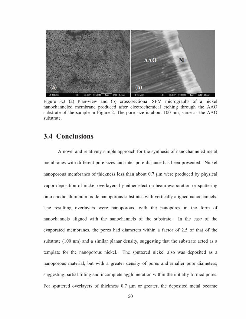
50
Figure 3.3 (a) Plan-view and (b) cross-sectional SEM micrographs of a nickel nanochanneled membrane produced after electrochemical etching through the AAO substrate of the sample in Figure 2. The pore size is about 100 nm, same as the AAO substrate.
3.4 Conclusions
A novel and relatively simple approach for the synthesis of nanochanneled metal
membranes with different pore sizes and inter-pore distance has been presented. Nickel
nanoporous membranes of thickness less than about 0.7 �m were produced by physical
vapor deposition of nickel overlayers by either electron beam evaporation or sputtering
onto anodic aluminum oxide nanoporous substrates with vertically aligned nanochannels.
The resulting overlayers were nanoporous, with the nanopores in the form of
nanochannels aligned with the nanochannels of the substrate. In the case of the
evaporated membranes, the pores had diameters within a factor of 2.5 of that of the
substrate (100 nm) and a similar planar density, suggesting that the substrate acted as a
template for the nanoporous nickel. The sputtered nickel also was deposited as a
nanoporous material, but with a greater density of pores and smaller pore diameters,
suggesting partial filling and incomplete agglomeration within the initially formed pores.
For sputtered overlayers of thickness 0.7 �m or greater, the deposited metal became
51
continuous, and electrochemical etching through the AAO substrate was used to on these
samples to produce the nanochannels. For all of the samples, the substrate could be
completely dissolved, resulting in free-standing metallic membranes.
3.5 Future Work
The nanosized features from the cross-sectional view of nanochanneled nickel
membrane can be investigated by SEM. The nanochanneled membranes with different
pore sizes can be fabricate and the morphology of the various pore size membranes will
also be examined by SEM. Large pore size membranes could be used to control
microfluidic flow, whereas small pore size memebranes could be employed as sensor
materials due to their high specific surface areas. If the pore size can be made to less than
20 nm, it is worthwhile to also test possible catalytic effects.
52
Bibliography
1. L. Liu, W. Lee, Z. Huang, R. Scholz, and U. Gosele: Fabrication and
characterization of a flow through nanoporous gold nanowire/AAO composite
membrane. Nanotechnology 19, 335604 (2008).
2. Y. Ding and J. Erlebacher: Nanoporous metals with controlled multimodal pore
size distribution. J. Am. Chem. Soc. 125, 7772 (2003).
3. Y. Ding, Y. J. Kim, and J. Erlebacher: Nanoporous gold leaf: “ancient
technology”/ advanced material. Adv. Mater. 16, 1897 (2004).
4. Z. Liu and P. C. Searson, Single nanoporous gold nanowire sensors. J. Phys.
Chem. B 110, 4318 (2006).
5. S. O. Kucheyev, J. R. Hayes, J. Biener, and T. Huser: Surface-enhanced Raman
scattering on nanoporous gold. Appl. Phys. Lett. 89, 053102 (2006).
6. L. H. Qian, X. Q. Yan, T. Fujita, A. Inoue, and M. W. Chen: Surface enhanced
Raman scattering of nanoporous gold: smaller pore sizes stronger enhancements.
Appl. Phys. Lett. 90, 153120 (2007).
7. C. X. Xu, J. X. Su, X. H. Xu, P. P. Liu, H. J. Zhao, F. Tian, and Y. Ding: Low
temperature CO oxidation over unsupported nanoporous Gold. J. Am. Chem. Soc.
129, 42 (2007).
8. J. Cai, J. Xu, J. Wang, L, Zhang, H. Zhou, Y. Zhong, D. Chen, H. Fan, H. Shao, J.
Zhang, and C.-N. Cao, Fabrication of three-dimensional nanoporous nickel films
with tunable nanoporosity and their excellent electrocatalytic activities for
hydrogen evolution reaction, International Journal of Hydrogen Energy 38, 934-
941 (2013).
53
9. J. Cabana, Z. Stoeva, J. J. Titman, D. H. Gregory, M. Rosa Palacin, Towards new
negative electrode materials for Li-ion batteries: electrochemical properties of
LiNiN. Chem. Mater. 20, 1676-1678 (2008).
10. O. A. Marina, L. R. Pederson, C. A. Coyle, E. C. Thomsen, P. Nachimuthu, and
D. J. Edwards, Electrochemical, structural and surface characterization of
nickel/zirconia solid oxide fuel cell anodes in coal gas containing antimony, J.
Power Sources 196, 4911-4922 (2011).
11. C. A. Marozzi and A. C. Chialvo, Development of electrode morphologies of
interest in electrocatalysis. Part 1: electrodeposited porous nickel electrodes,
Electrochem. Acta. 45, 2111-2120 (2000).
12. Yan-Yan Gao, Ai-Juan Han, Fang Miao, Guang-Lan Li, Hui Li, Zuo-Shan Zhang,
and Shu-Yong Zhang: Preparation of metallic nanopore arrays using template-
guided electrochemical etching, Mater. Lett. 64, 1028-1030 (2010).
13. K. Nice and J. Strickland, How Fuel Cells Work, September 18, 2000.
HowStuffWorks.com.
URL:http://auto.howstuffworks.com/fuel-efficiency/alternative-fuels/fuel-cell.htm
14. H. Masuda, K. Nishio, and N. Baba, Fabrication of Porous TiO2 Films Using
Two-Step Replication of Microstructure of Anodic Alumina, Jpn. J. Appl. Phyc.
31, L1775-L1777 (1992).
54
15. H. Masuda and K. Fukuda, Ordered Metal Nanohole Arrays Made by a Two-Step
Replication of Honeycomb Structures of Anodic Alumina, Science 268 (5216),
1466-1468 (1995).
16. P. Hoyer, N. Baba, and H. Masuda, Small quantum-sized CdS particles assembled
to form a regularly nanostructured porous film, Appl. Phys. Lett. 66, 2700 (1995).
17. Y. Lei, W.K. Chim, Z. Zhang, T. Zhou, L. Zhang, G. Meng, and F. Phillipp,
Ordered nanoporous nickel films and their magnetic properties, Chem. Phys. Lett.
380, 313-318 (2003).
18. D0 Mukherji, G0 Pigozzi, F0 Schmitz, O0 Näth, J0 Rösler1,and G0 Kostorz, Nano-
structured materials produced from simple metallic alloys by phase separation1,Nanotechnology 16, 2176 (2005).
19. C. Ji and P. C. Searson, Synthesis and Characterization of Nanoporous Gold
Nanowires, J. Phys. Chem. B 107 (19), pp 4494–4499 (2003).
20. F. Jia, C. Yu, K. Deng, and L. Zhang, Nanoporous Metal (Cu, Ag, Au) Films with
High Surface Area: General Fabrication and Preliminary Electrochemical
Performance, J. Phys. Chem. C 111, 8424-8431 (2007).
55
Chapter 4
Purification and Refinement of Single-Walled
Carbon Nanotubes (SWCNTs) by AC
Dielectrophoresis
4.1 Introduction
Since the success of integrated silicon technology of metal oxide semiconductor
field-effect transistor (MOSFET), the ability to scale down the dimensions of the device
has been the key to improving speed and energy efficiency.1-2 However, industry
generally expects that fundamental material barriers will limit the size reduction of
current nanoscale MOSFET devices and that this road block to continuing advancement
will arrive within a decade as predicted by Moore’s law.2 In order to overcome these
barriers, new materials are needed to solve the scalability problems of future silicon
devices. Among these new silicon substitute materials, single-walled carbon nanotubes
(SWCNTs) have become excellent candidates as building blocks for future nanoscale
electronics due to their small size and unique electrical properties. In 2012, the New York
Times reported on the future of single-walled carbon nanotubes (SWCNTs) as a
successor of silicon. IBM’s director of physical sciences, Dr. Supratik Guha, at the
56
company’s Yorktown Heights, NY research center was quoted as saying that “these
carbon nanotube based devices outperformed any other switches made from any other
material, including silicon.”3
SWCNTs have been actively pursued as electronic materials and silicon device
substitutes since Ijima and Bethune independently discovered them in 1993.1-2,4-5
However, current SWCNT production techniques generate a mixture of two types of
nanotubes with divergent electrical behaviors. Some of the nanotubes act as metallic
materials, while others display semiconducting properties. This as-synthesized random
mixture has complicated the realization of functional carbon nanotube-based
nanoelectronics.4,6-7 Here we report a method of separating metallic SWCNTs from
semiconducting ones from an initially random mixture of SWCNTs in suspension using
AC dielectrophoresis (DEP). The goal of this project is to fabricate a microfluidic lab-
on-a-chip device that can continuously purify, sort and collect industrially relevant
quantity of metallic and semiconducting SWCNTs.
This technique separates metallic SWCNTs from semiconducting ones due to the
difference in the magnitude and direction of dielectrophoretic forces experienced by the
two types of nanotubes. The large difference in force is related to the fact that metallic
SWCNTs display a large absolute dielectric constant and semiconducting SWCNTs
display a corresponding low value, as reported by Krupke and co-workers.4 It is noted
that sorted SWCNTs have great commercial value. Currently, sorted 98% pure
semiconducting nanotubes cost $520 per mg and sorted 98% pure metallic tubes cost
$788 per mg.8
57
4.1.1 Single-Walled Carbon Nanotubes (SWCNTs)
A single-walled carbon nanotube (SWCNT) can be considered to be a single
rolled-up graphene sheet with its ends folded to form a seamless hollow cylinder.9
SWCNTs are nanostructures with dimensions of about 1 nm in diameter and lengths are
about a few microns to centimeter range.10 A SWCNT can be mathematically represented
as the chiral vector, C. The definition of the chiral vector comes from treating the
circumference of a nanotube as two crystallographically equivalent sites of a two-
dimensional (2-D) grapheme sheet.11 The chiral vector, C, is written as
2 � 34� 5 647, (4.1)
where (n, m) are integers called chiral vector and a1 and a2 are unit vectors of the
hexagonal honeycomb lattice. For example, a (4, 4) chiral vector nanotube is described in
Figure 4.1.11 Chiral vectors can also be related to the electronic types of SWCNTs as
shown in Figure 4.2. SWCNTs exhibit either metallic or semiconducting behaviors
depending on diameter and orientation of carbon hexagons with respect to the tube axis
(degree of chirality).9,13 Dresselhaus et al. reported that when 3 � 6 � #�, SWCNTs can
be classified as metallic tubes due to the change of singularities in the 1D density of
states as determined from a quasi-continuum and theoretical calculation.14-15 On the other
hand, SWCNTs is semiconducting when 3 � 6 8 #�, where q is an integer in both
cases.9,13-15 In general, the diameter of a SWCNT can be mathematically represented in
terms of integers (n, m) as
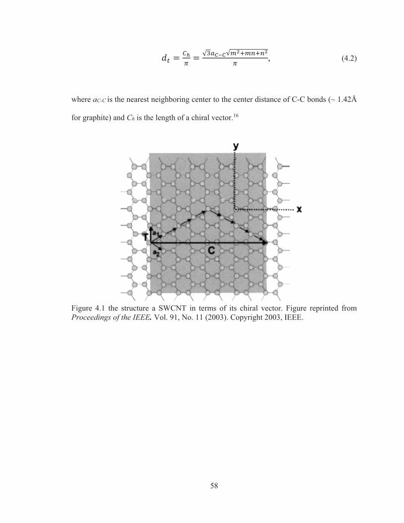
58
$) � 9:; � ���<� ����=�=�
; , (4.2)
where aC-C is the nearest neighboring center to the center distance of C-C bonds (~ 1.42Å
for graphite) and Ch is the length of a chiral vector.16
Figure 4.1 the structure a SWCNT in terms of its chiral vector. Figure reprinted from Proceedings of the IEEE. Vol. 91, No. 11 (2003). Copyright 2003, IEEE.
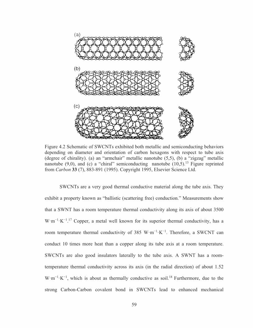
59
Figure 4.2 Schematic of SWCNTs exhibited both metallic and semiconducting behaviors depending on diameter and orientation of carbon hexagons with respect to tube axis (degree of chirality). (a) an “armchair” metallic nanotube (5,5), (b) a “zigzag” metallic nanotube (9,0), and (c) a “chiral” semiconducting nanotube (10,5).13 Figure reprinted from Carbon 33 (7), 883-891 (1995). Copyright 1995, Elsevier Science Ltd.
SWCNTs are a very good thermal conductive material along the tube axis. They
exhibit a property known as “ballistic (scattering free) conduction.” Measurements show
that a SWNT has a room temperature thermal conductivity along its axis of about 3500
W·m1·K1.17 Copper, a metal well known for its superior thermal conductivity, has a
room temperature thermal conductivity of 385 W·m1·K1. Therefore, a SWCNT can
conduct 10 times more heat than a copper along its tube axis at a room temperature.
SWCNTs are also good insulators laterally to the tube axis. A SWNT has a room-
temperature thermal conductivity across its axis (in the radial direction) of about 1.52
W·m1·K1, which is about as thermally conductive as soil.18 Furthermore, due to the
strong Carbon-Carbon covalent bond in SWCNTs lead to enhanced mechanical
60
properties. SWCNTs have Young’s modulus about ten times higher than that of steel.
This strong covalent bonding also leads to the near defect free structure of SWCNTs.11
SWCNTs are also chemical inert to most of solvent and carbon is a very light weight
material.
In addition, variability during production of SWCNTs leads to tubes of different
diameter and atomic configuration relative to the tube axis (degree of chirality).2,9 These
structural variations dictate the electronic properties of SWCNTs and can result in
metallic or semiconducting nanotubes as shown in Figure 4.2. It is known that
approximately 7� of the SWCNTs are semiconducting and about �� of the SWCNTs are
metallic from a single production.9,12 The metallic behavior of SWCNTs comes from the
small opening energy gap at the Fermi level due to the curvature of the graphene sheet.14
Since SWCNTs are 1-D systems resulting reduced phase space for electron carrier
scattering, the tubes have much lower resistivity than 3-D structures. Therefore, energy
dissipation of a semiconducting SWCNT is minimal. As a result, semiconducting
SWCNTs have the advantage to use carbon nanotubes in field-effect transistor (FET)
technologies. Meanwhile, metallic SWCNTs can carry current densities 2 to 3 orders of
magnitude higher than Cu or Al, such as 109 A/cm2.19 The unique properties can allow
metallic SWCNTs to be a good candidate of interconnect of nanoelectronics.20-21
However, with so many excellent and unique, mechanical, chemical, thermal, and
electronic properties, there are challenges in producing SWCNT-based devices. The main
reason is that there is no known synthesis method that can control SWCNTs with similar
diameters and electronic properties as determined by chirality. The current technology
can only produce polydisperse SWCNTs with different chirality. Therefore, it is
61
important and more efficient to develop effective purification and separation methods
until the controllable synthesis method is achieved, whether separating by metallic from
semiconducting, sorting by diameter, or in terms of chirality. In this chapter, the focus
will be to address on the fabrication a microfluidic device that can continuously collect
and sort the initial mixed electronic types of SWCNTs into individual groups of refined
metallic or semiconducting SWCNTs. By doing so, this separating device can be used as
a very effective tool to scale up the supply of refined and purified metallic or
semiconducting SWCNTs to an industrial relevant quantity in order to make CNT-based
electronics to reach commercial reality.
4.1.2 AC Dielectrophoresis on Single-Walled
Carbon Nanotubes
Dielectrophoresis (DEP) is an electro-kinetic phenomenon where a non-uniform
electric field induces polarization in a neutrally charged particle and causes motion of the
induced dipole.8 That is, in an AC and nonuniform electric field, depending on the
polarizability of the particle compared to that of the medium, the dielectrophoretic (DEP)
force could push the material toward the direction of the electric field gradient (positive
DEP force) or against field gradient (negative DEP force).22-24 The dielectrophoretic force
exerted on a polarized particle in a nonuniform electric field in suspension can be written
as:
>?@A � BC D E/F, (4.3)
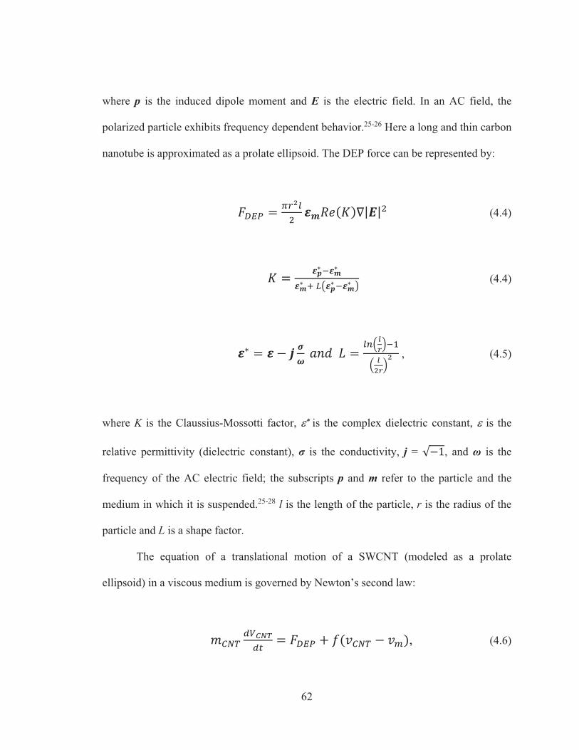
62
where p is the induced dipole moment and E is the electric field. In an AC field, the
polarized particle exhibits frequency dependent behavior.25-26 Here a long and thin carbon
nanotube is approximated as a prolate ellipsoid. The DEP force can be represented by:
>?@A � ;G�*7 HI&JBK/ELFL7 (4.4)
K � HCM�HIMHIM �,NOHCM�HIM P (4.4)
HM � H � Q RS ,43$,,T � *=UV
WX��U V�WX
� , (4.5)
where K is the Claussius-Mossotti factor, ���is the complex dielectric constant, � is the
relative permittivity (dielectric constant), � is the conductivity, j = �Y, and � is the
frequency of the AC electric field; the subscripts p and m refer to the particle and the
medium in which it is suspended.25-28 l is the length of the particle, r is the radius of the
particle and L is a shape factor.
The equation of a translational motion of a SWCNT (modeled as a prolate
ellipsoid) in a viscous medium is governed by Newton’s second law:
69Z ���[��) � >?@A 5 \B]9Z � ]�/, (4.6)
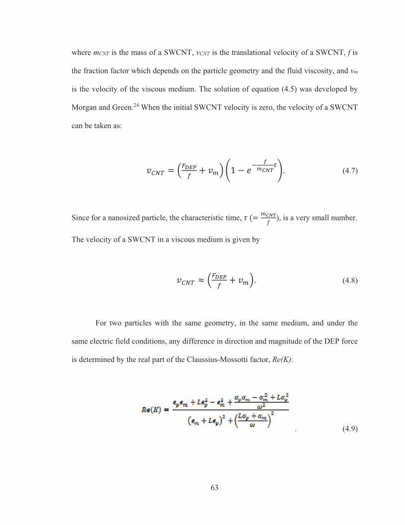
63
where mCNT is the mass of a SWCNT, vCNT is the translational velocity of a SWCNT, f is
the fraction factor which depends on the particle geometry and the fluid viscosity, and vm
is the velocity of the viscous medium. The solution of equation (4.5) was developed by
Morgan and Green.24 When the initial SWCNT velocity is zero, the velocity of a SWCNT
can be taken as:
]9Z � U _̂`ab 5 ]�XcY � J� d
e�[�)f. (4.7)
Since for a nanosized particle, the characteristic time, g,B� ��[�b ), is a very small number.
The velocity of a SWCNT in a viscous medium is given by
]9Z h U _̂`ab 5 ]�X. (4.8)
For two particles with the same geometry, in the same medium, and under the
same electric field conditions, any difference in direction and magnitude of the DEP force
is determined by the real part of the Claussius-Mossotti factor, Re(K):
. (4.9)
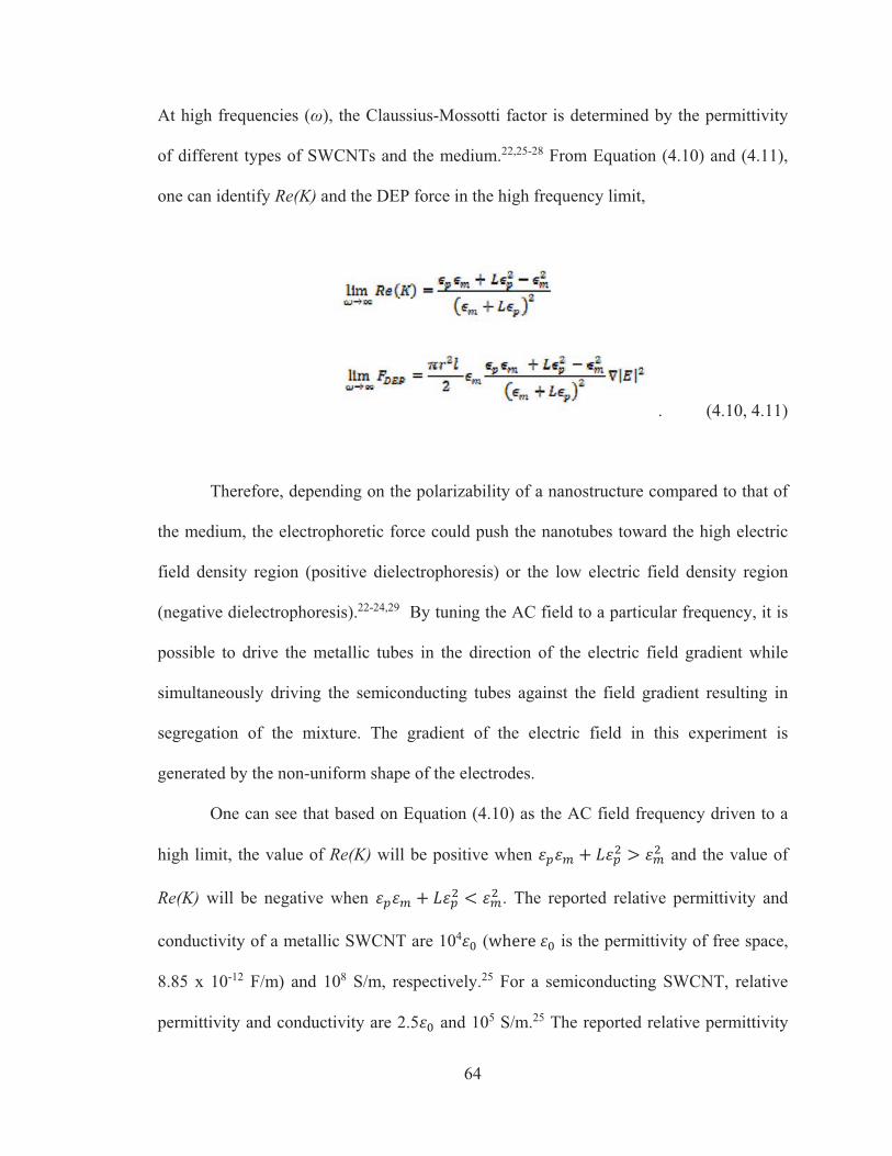
64
At high frequencies (�), the Claussius-Mossotti factor is determined by the permittivity
of different types of SWCNTs and the medium.22,25-28 From Equation (4.10) and (4.11),
one can identify Re(K) and the DEP force in the high frequency limit,
. (4.10, 4.11)
Therefore, depending on the polarizability of a nanostructure compared to that of
the medium, the electrophoretic force could push the nanotubes toward the high electric
field density region (positive dielectrophoresis) or the low electric field density region
(negative dielectrophoresis).22-24,29 By tuning the AC field to a particular frequency, it is
possible to drive the metallic tubes in the direction of the electric field gradient while
simultaneously driving the semiconducting tubes against the field gradient resulting in
segregation of the mixture. The gradient of the electric field in this experiment is
generated by the non-uniform shape of the electrodes.
One can see that based on Equation (4.10) as the AC field frequency driven to a
high limit, the value of Re(K) will be positive when iji� 5 Tij7 k i�7 and the value of
Re(K) will be negative when iji� 5 Tij7 l i�7 . The reported relative permittivity and
conductivity of a metallic SWCNT are 104im (nopqp,im is the permittivity of free space,
8.85 x 10⁻¹² F/m) and 108 S/m, respectively.25 For a semiconducting SWCNT, relative
permittivity and conductivity are 2.5im and 105 S/m.25 The reported relative permittivity
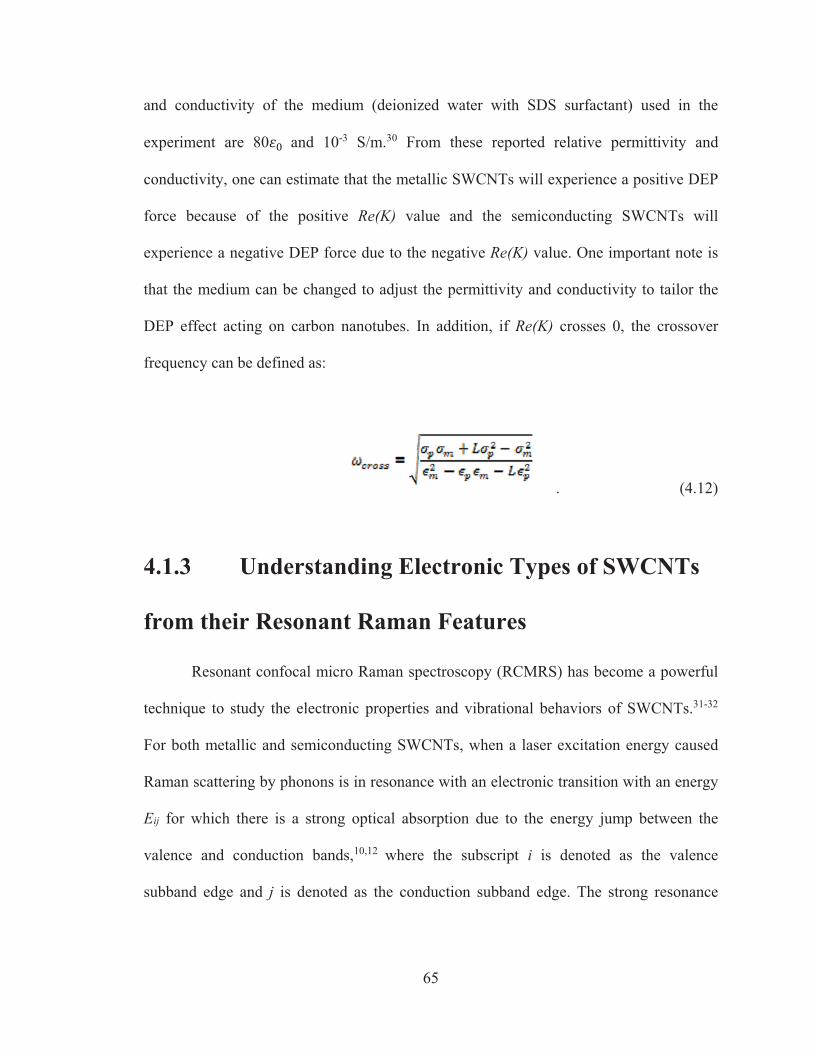
65
and conductivity of the medium (deionized water with SDS surfactant) used in the
experiment are 80im and 10-3 S/m.30 From these reported relative permittivity and
conductivity, one can estimate that the metallic SWCNTs will experience a positive DEP
force because of the positive Re(K) value and the semiconducting SWCNTs will
experience a negative DEP force due to the negative Re(K) value. One important note is
that the medium can be changed to adjust the permittivity and conductivity to tailor the
DEP effect acting on carbon nanotubes. In addition, if Re(K) crosses 0, the crossover
frequency can be defined as:
. (4.12)
4.1.3 Understanding Electronic Types of SWCNTs
from their Resonant Raman Features
Resonant confocal micro Raman spectroscopy (RCMRS) has become a powerful
technique to study the electronic properties and vibrational behaviors of SWCNTs.31-32
For both metallic and semiconducting SWCNTs, when a laser excitation energy caused
Raman scattering by phonons is in resonance with an electronic transition with an energy
Eij for which there is a strong optical absorption due to the energy jump between the
valence and conduction bands,10,12 where the subscript i is denoted as the valence
subband edge and j is denoted as the conduction subband edge. The strong resonance
66
condition allows scientists and engineers to obtain large Raman signaling enhancements
due to this enhanced coupling between electrons and phonons of SWCNTs.
Two features of signature wavenumbers of Raman spectra are used to identify the
electronic properties of SWCNTs. The radial breathing mode (RBM) represents the laser
excited vibration of carbon atoms in phase in the radial direction relative to the nanotube
axis.9 The radial breathing mode (RBM) region usually occurs at the frequencies of 100
to 350 cm-1 for SWCNTs31 and according to Araujo et al. and Dresselhaus et al., the
RBM frequency, �RBM, is depended on the reciprocal of the carbon nanotube diameter,
dt.10,32-35
rstu � v�w 5 x, (4.13)
where A and B are constants and vary between individual tubes and bundle tubes from
experimental observations.16,33-34,36 The constant A is also in the diameter
determination.20,47 The RBM frequency is independent of the chiral angle.9
Metallic SWCNTs have RBM wavenumbers in the range of 220 - 300 cm-1 with a
laser excitation wavelength of 514.5 nm (2.41 eV). Semiconducting SWCNTs have RBM
wavenumbers in the range of 170 - 220 cm-1 with a laser excitation wavelength of 514.5
nm.10,29,37 The wavenumbers of RBM peaks also provide information on chirality, which
is related to the electronic properties of SWCNTs. Li et al. summarized this reciprocal
dependence between RBM frequency and carbon nanotube diameter is valid when the
tube diameter is larger than 0.7 nm.38 However, when the diameter of a SWCNT is
67
getting smaller, the reciprocal dependence will become invalid due to the induced
curvature effect.38-39
The G-band mode (tangential mode) is related to vibrations in all sp2 carbon
materials.36 The characteristic Raman features and lineshape of the G-band mode
corresponds to the electronic properties (semiconducting or metallic) of SWCNTs.16 In
general, as shown in the reference Raman spectra in Figure 4.11, the Raman spectra of
semiconducting SWCNTs show a sharp peak at 1592 cm-1 for the G-band mode, while
metallic SWCNTs generate a broad peak at 1582 cm-1 for the G-band mode.9,16,29,31,37,40-41
The G band is also reported to be constructed by two components, the lower frequency
component associated with vibrations along the circumferential direction (G-) and the
higher frequency component attributed to vibrations along the direction of the tube axis
(G+).36
Since the response for laser excitation with varied wavelength reveal very
different Raman spectra for each sample,41-43 the Kataura plot is used to relate different
laser excitation levels to the diameter of SWCNTs and the Raman shift wavenumber of
corresponding resonance scattering nanotubes.44 One important note is that according to
the Kataura plot, there is a possibility that a single SWCNT can be evaluated as a metallic
or semiconducting nanotubes by using different energy lasers. Therefore, significant
errors may occur if one does not carefully use the same wavelength laser in the
experiment because each analysis can give different optical properties.
68
4.2 Experimental
4.2.1 Static System
This section is an adapted reproduction from Su Chih Chi, Robert C. Cammarata, Chia-
Ling Chien, Donglei Fan, Stephen Farias, and Danru Qu, inventors, Johns Hopkins
University, assignee, “Systems and Methods for Separating Metallic and Nonmetallic
Particles in a Mixed-Particle Suspension,” U. S. Patent Provisional Application No.
13/902,191, Filling date: May 24, 2013.
Single-walled carbon nanotubes (SWCNTs) purchased from Sigma-Aldrich
(carbon > 90%, � 70% carbon as SWCNT) were used in this study. Suspensions were
prepared by mixing 2 mg of raw SWCNTs roots in 20 ml deionized water with 1 wt.% of
the surfactant sodium dodecyl sulfate (SDS) (99.0%, Sigma-Aldrich). The suspension
was ultra-sonicated for 30 minutes and then centrifuged at 3000 rpm for 2 hours. The
upper 80% of the suspension was taken to use in the experiment. To obtain the non-
uniform electric field required for dielectrophoresis, a gold microelectrode (MaxTek, Inc.
P/N 149272-1) composed of a circular inner electrode of radius of about 3.3 mm and a
semicircular outer electrode of radius of about 9 mm as shown in Figure 1 was used in
the experiments. The electrodes provided a radial electric field gradient to establish a
radially directed dielectrophoretic force. The SWCNTs separation device is connected to
a HP E3617A DC power supply and an Agilent Technologies 33120A 15 MHz function
waveform generator. After the function generator was switched on, a drop of suspension
(~ 100 �L) was released into the gap between the circular inner and semicircular outer
electrodes.
69
The separation was operated at a frequency of 10 MHz and a peak-to-peak
voltage of 10 Vp-p between the two electrodes. After the voltage was applied, the
suspension was allowed to rest and air dry for ~ 4 hours and samples were collected from
each electrode. To confirm the segregation of metallic and semiconducting SWCNTs,
resonant Raman spectroscopy was performed since the difference in optical properties
between metallic and semiconducting SWCNTs allows the spectral peaks of each species
in the Raman data to be resolved distinguishably16. The G-band and radial breathing
mode (RBM) frequencies of metallic and semiconducting SWCNTs were identified using
the Ar+ ion laser excitation energy of 2.41 eV (514 nm). The Raman spectra at position 1
(SWCNTs are near the circular inner electrode) and position 4 (SWCNTs are near the
semicircular outer electrode) were generated by an Ocean Optics QE65000 Raman
scientific-grade spectrometer equipped with a Mitutoyo microscope and a
thermoelectrically cooled charge-coupled device (CCD). The Raman spectra at position 2
(SWCNTs are about 5 �m away from the circular inner electrode) and position 3
(SWCNTs are about 300 �m away from the circular inner electrode) were generated by a
HORIBA Scientific Raman system.
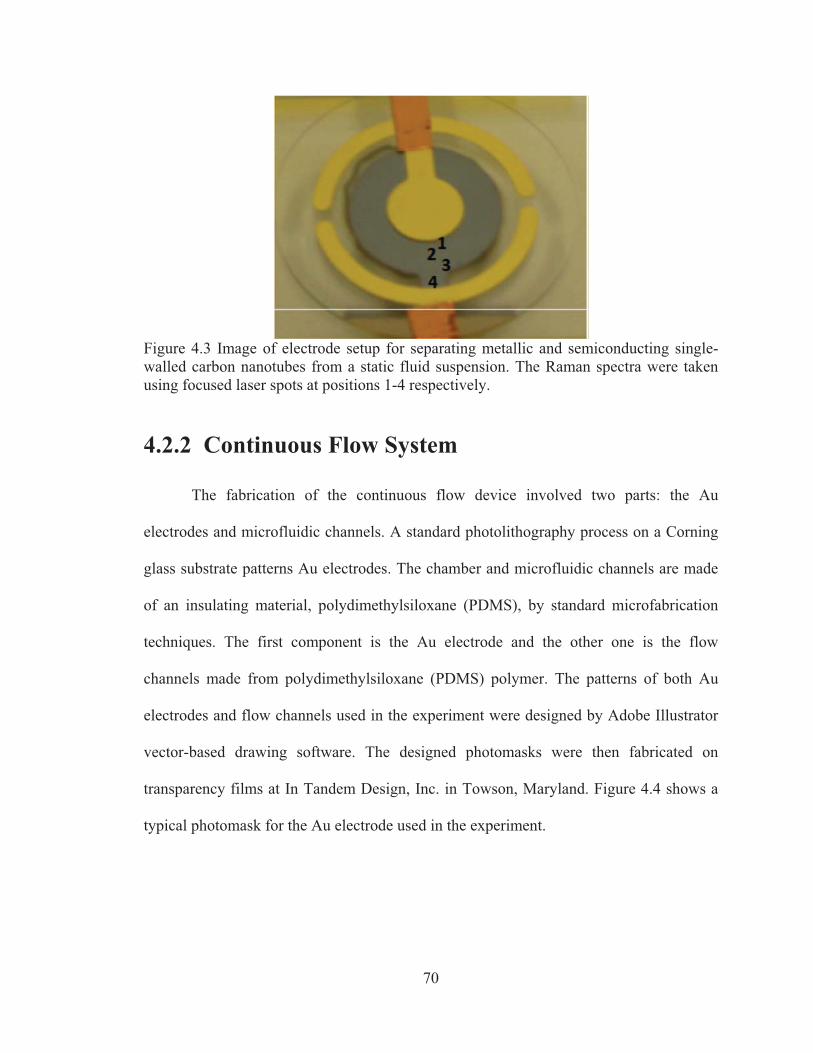
70
Figure 4.3 Image of electrode setup for separating metallic and semiconducting single-walled carbon nanotubes from a static fluid suspension. The Raman spectra were taken using focused laser spots at positions 1-4 respectively.
4.2.2 Continuous Flow System
The fabrication of the continuous flow device involved two parts: the Au
electrodes and microfluidic channels. A standard photolithography process on a Corning
glass substrate patterns Au electrodes. The chamber and microfluidic channels are made
of an insulating material, polydimethylsiloxane (PDMS), by standard microfabrication
techniques. The first component is the Au electrode and the other one is the flow
channels made from polydimethylsiloxane (PDMS) polymer. The patterns of both Au
electrodes and flow channels used in the experiment were designed by Adobe Illustrator
vector-based drawing software. The designed photomasks were then fabricated on
transparency films at In Tandem Design, Inc. in Towson, Maryland. Figure 4.4 shows a
typical photomask for the Au electrode used in the experiment.
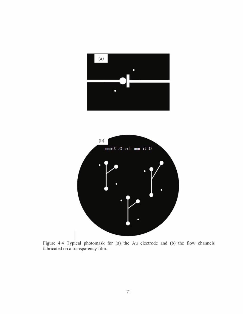
71
Figure 4.4 Typical photomask for (a) the Au electrode and (b) the flow channels fabricated on a transparency film.
(a)
(b)
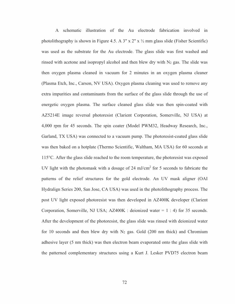
72
A schematic illustration of the Au electrode fabrication involved in
photolithography is shown in Figure 4.5. A 3" x 2" x ½ mm glass slide (Fisher Scientific)
was used as the substrate for the Au electrode. The glass slide was first washed and
rinsed with acetone and isopropyl alcohol and then blew dry with N2 gas. The slide was
then oxygen plasma cleaned in vacuum for 2 minutes in an oxygen plasma cleaner
(Plasma Etch, Inc., Carson, NV USA). Oxygen plasma cleaning was used to remove any
extra impurities and contaminants from the surface of the glass slide through the use of
energetic oxygen plasma. The surface cleaned glass slide was then spin-coated with
AZ5214E image reversal photoresist (Clarient Corporation, Somerville, NJ USA) at
4,000 rpm for 45 seconds. The spin coater (Model PWM32, Headway Research, Inc.,
Garland, TX USA) was connected to a vacuum pump. The photoresist-coated glass slide
was then baked on a hotplate (Thermo Scientific, Waltham, MA USA) for 60 seconds at
115°C. After the glass slide reached to the room temperature, the photoresist was exposed
UV light with the photomask with a dosage of 24 mJ/cm2 for 5 seconds to fabricate the
patterns of the relief structures for the gold electrode. An UV mask aligner (OAI
Hydralign Series 200, San Jose, CA USA) was used in the photolithography process. The
post UV light exposed photoresist was then developed in AZ400K developer (Clarient
Corporation, Somerville, NJ USA; AZ400K : deionized water = 1 : 4) for 35 seconds.
After the development of the photoresist, the glass slide was rinsed with deionized water
for 10 seconds and then blew dry with N2 gas. Gold (200 nm thick) and Chromium
adhesive layer (5 nm thick) was then electron beam evaporated onto the glass slide with
the patterned complementary structures using a Kurt J. Lesker PVD75 electron beam
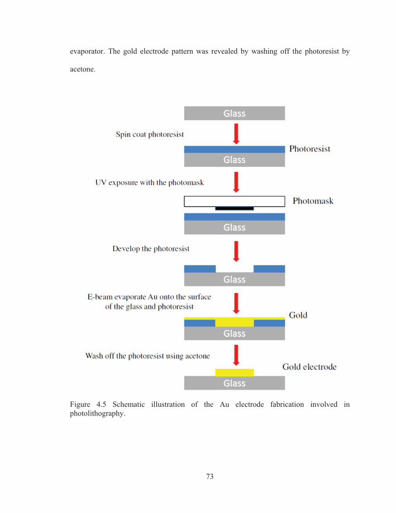
73
evaporator. The gold electrode pattern was revealed by washing off the photoresist by
acetone.
Figure 4.5 Schematic illustration of the Au electrode fabrication involved in photolithography.
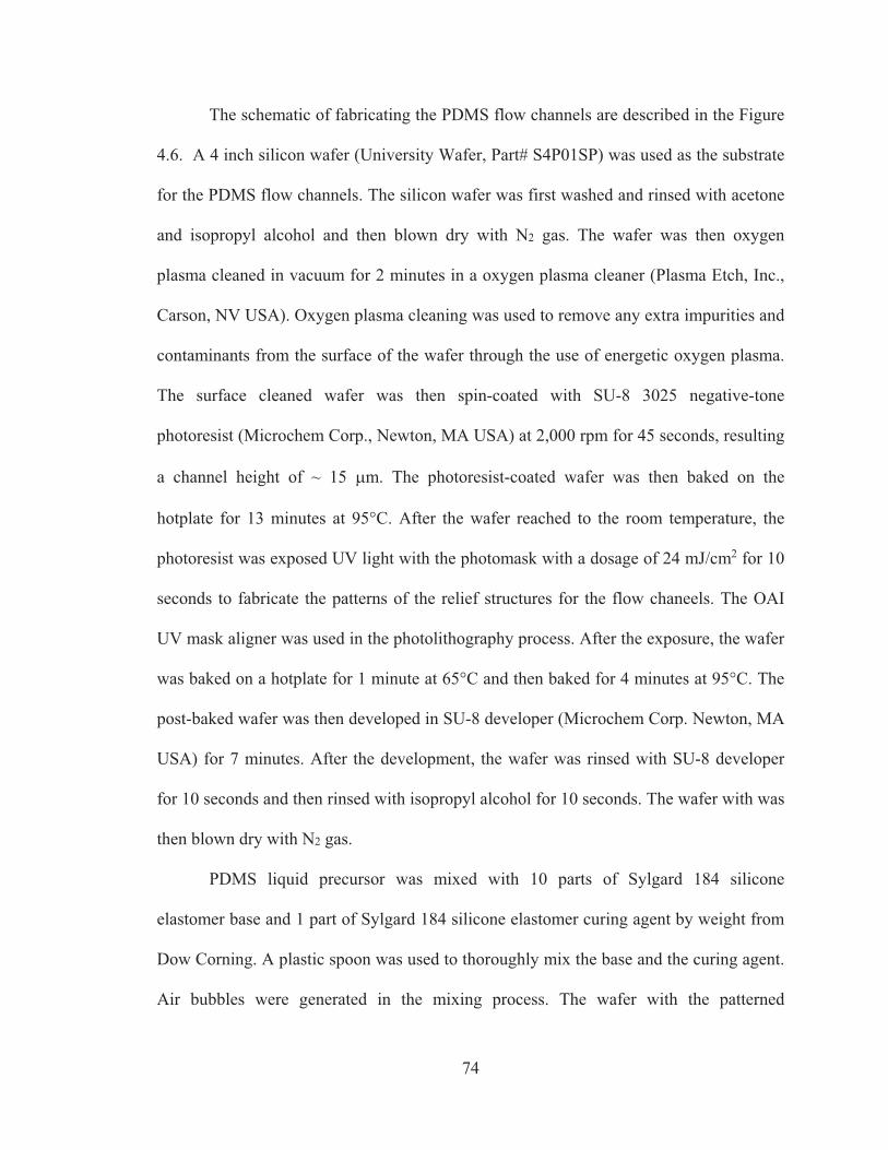
74
The schematic of fabricating the PDMS flow channels are described in the Figure
4.6. A 4 inch silicon wafer (University Wafer, Part# S4P01SP) was used as the substrate
for the PDMS flow channels. The silicon wafer was first washed and rinsed with acetone
and isopropyl alcohol and then blown dry with N2 gas. The wafer was then oxygen
plasma cleaned in vacuum for 2 minutes in a oxygen plasma cleaner (Plasma Etch, Inc.,
Carson, NV USA). Oxygen plasma cleaning was used to remove any extra impurities and
contaminants from the surface of the wafer through the use of energetic oxygen plasma.
The surface cleaned wafer was then spin-coated with SU-8 3025 negative-tone
photoresist (Microchem Corp., Newton, MA USA) at 2,000 rpm for 45 seconds, resulting
a channel height of ~ 15 �m. The photoresist-coated wafer was then baked on the
hotplate for 13 minutes at 95°C. After the wafer reached to the room temperature, the
photoresist was exposed UV light with the photomask with a dosage of 24 mJ/cm2 for 10
seconds to fabricate the patterns of the relief structures for the flow chaneels. The OAI
UV mask aligner was used in the photolithography process. After the exposure, the wafer
was baked on a hotplate for 1 minute at 65°C and then baked for 4 minutes at 95°C. The
post-baked wafer was then developed in SU-8 developer (Microchem Corp. Newton, MA
USA) for 7 minutes. After the development, the wafer was rinsed with SU-8 developer
for 10 seconds and then rinsed with isopropyl alcohol for 10 seconds. The wafer with was
then blown dry with N2 gas.
PDMS liquid precursor was mixed with 10 parts of Sylgard 184 silicone
elastomer base and 1 part of Sylgard 184 silicone elastomer curing agent by weight from
Dow Corning. A plastic spoon was used to thoroughly mix the base and the curing agent.
Air bubbles were generated in the mixing process. The wafer with the patterned
75
complementary structures was firstly placed in a Petri dish. Then the liquid PDMS
mixture was poured onto the surface of the wafer until the whole surface was covered by
the mixture and the desired thickness of the fluid level was reached. The Petri dish
containing both the wafer and PDMS prepolymer was then placed in a dessicator and
connected to the vacuum line until all the bubbles disappeared. After all the bubbles were
gone, the Petri dish was placed in an oven set to 80°C and cured it for 30 minutes. After
the curing, nylons tubes (McMater, Robbinsiville, NJ) that are to serve as reservoirs to
collect the sorted carbon nanotubes were carefully placed at the desired spots of channel
outlets. After the reservoirs were placed, PDMS liquid precursor mixed with 10 parts of
Sylgard 184 silicone elastomer base and 1 part of Sylgard 184 silicone elastomer curing
agent by weight was poured into the Petri dish as the top layer to seal the reservoirs. It is
important to repeat the step of removing air bubbles in the dessicator and curing the
prepolymer in the oven. The block with flow channels was cut into PDMS with the
desired dimensions using a scalpel and carefully separated and peeled the PDMS block
off from the silicon wafer.
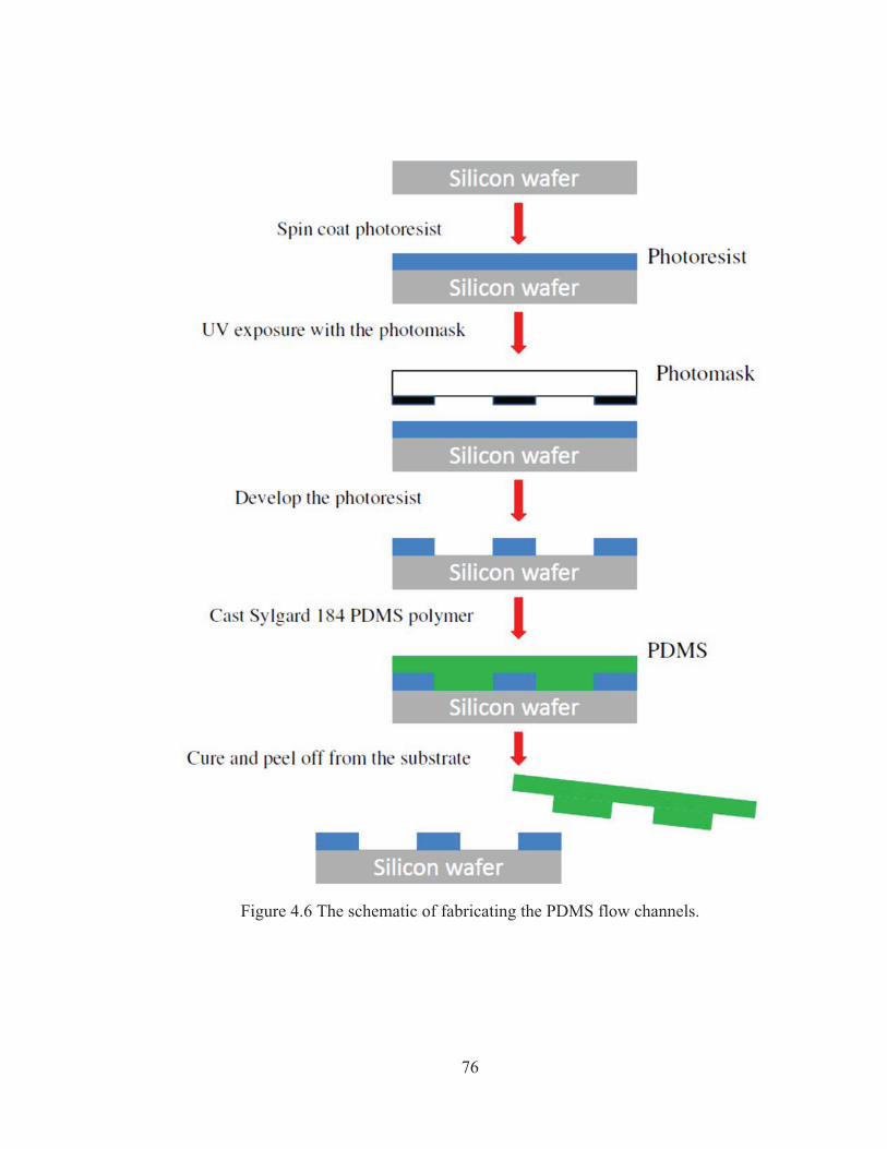
76
Figure 4.6 The schematic of fabricating the PDMS flow channels.
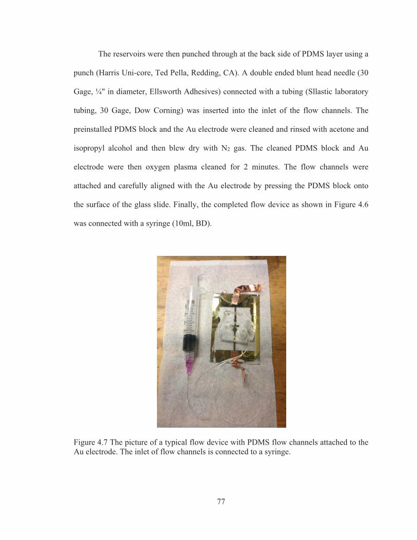
77
The reservoirs were then punched through at the back side of PDMS layer using a
punch (Harris Uni-core, Ted Pella, Redding, CA). A double ended blunt head needle (30
Gage, ¼" in diameter, Ellsworth Adhesives) connected with a tubing (Sllastic laboratory
tubing, 30 Gage, Dow Corning) was inserted into the inlet of the flow channels. The
preinstalled PDMS block and the Au electrode were cleaned and rinsed with acetone and
isopropyl alcohol and then blew dry with N2 gas. The cleaned PDMS block and Au
electrode were then oxygen plasma cleaned for 2 minutes. The flow channels were
attached and carefully aligned with the Au electrode by pressing the PDMS block onto
the surface of the glass slide. Finally, the completed flow device as shown in Figure 4.6
was connected with a syringe (10ml, BD).
Figure 4.7 The picture of a typical flow device with PDMS flow channels attached to the Au electrode. The inlet of flow channels is connected to a syringe.
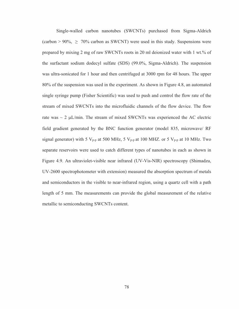
78
Single-walled carbon nanotubes (SWCNTs) purchased from Sigma-Aldrich
(carbon > 90%, � 70% carbon as SWCNT) were used in this study. Suspensions were
prepared by mixing 2 mg of raw SWCNTs roots in 20 ml deionized water with 1 wt.% of
the surfactant sodium dodecyl sulfate (SDS) (99.0%, Sigma-Aldrich). The suspension
was ultra-sonicated for 1 hour and then centrifuged at 3000 rpm for 48 hours. The upper
80% of the suspension was used in the experiment. As shown in Figure 4.8, an automated
single syringe pump (Fisher Scientific) was used to push and control the flow rate of the
stream of mixed SWCNTs into the microfluidic channels of the flow device. The flow
rate was ~ 2 �L/min. The stream of mixed SWCNTs was experienced the AC electric
field gradient generated by the BNC function generator (model 835, microwave/ RF
signal generator) with 5 Vp-p at 500 MHz, 5 Vp-p at 100 MHZ. or 5 Vp-p at 10 MHz. Two
separate reservoirs were used to catch different types of nanotubes in each as shown in
Figure 4.9. An ultraviolet-visible near infrared (UV-Vis-NIR) spectroscopy (Shimadzu,
UV-2600 spectrophotometer with extension) measured the absorption spectrum of metals
and semiconductors in the visible to near-infrared region, using a quartz cell with a path
length of 5 mm. The measurements can provide the global measurement of the relative
metallic to semiconducting SWCNTs content.
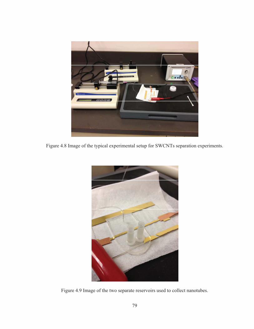
79
Figure 4.8 Image of the typical experimental setup for SWCNTs separation experiments.
Figure 4.9 Image of the two separate reservoirs used to collect nanotubes.
80
4.3 Results and Discussion
4.3.1. Static System
Figure 4.3 shows positions where Raman spectra were taken. Raman spectra of
SWCNTs at position 1 and position 4 are shown in Figure 4.10. Comparing the measured
Raman spectra to reference Raman spectra shown in Figure 4.11 generated by
Dresselhaus et al., the spectra of the D and G bands from positions 1 and 4 matches well
with the spectra for purified metallic tubes and purified semiconducting tubes
respectively.
The radial breathing mode (RBM) region usually occurs at the frequencies of 100
to 350 cm-1 for SWCNTs31 and according to Araujo et al. and Dresselhaus et al., the
RBM frequency, RBM, is depended on the reciprocal of the carbon nanotube diameter,
dt.10,32-34 The wavenumbers of RBM peaks also provide information on chirality, which is
related to the electronic properties of SWCNTs. Li et al. summarized this reciprocal
dependence between RBM frequency and carbon nanotube diameter is valid when the
tube diameter is larger than 0.7 nm.38 However, when the diameter of a SWCNT becomes
smaller, the reciprocal dependence will become invalid due to the induced curvature
effect.38-39
In Figure 4.10, for laser excitation energy of 2.41 eV (514 nm), the Raman spectra
of SWCNTs near the semicircular outer electrode (position 4) show a sharp peak at 267
cm-1. This peak indicates the possible presence of some metallic SWCNTs around the
area despite the dominant semiconducting signal. The Raman profiles of SWCNTs near
the circular inner electrode (position 1) do not show any peaks in the RBM region.
81
Instead, a flat and broad curve is revealed in this region. This may be due to a high local
concentration of SDS surfactant that affects the Raman spectra at the RBM
wavenumbers.
G-band mode is related to vibrations in all sp2 carbon materials. The characteristic
Raman peak of the G-band mode corresponds to the electronic properties
(semiconducting or metallic) of SWCNTs.24 In general, as shown in the reference Raman
spectra in Figure 4.11, the Raman spectra of semiconducting SWCNTs show a sharp
peak at 1592 cm-1 for the G-band mode, while metallic SWCNTs generate a broad peak
at 1582 cm-1 for the G-band mode.16,29,31,37,40-41 The G-band mode signal of the tubes near
the semicircular outer electrode (position 4) shows a sharp peak at 1591 cm-1. The G-
band mode signal of the tubes near the circular inner electrode area (position 1) shows a
sharp peak at 1585 cm-1. The SWCNTs at position 1 are metallic after the separation
experiment. At position 4, the SWCNTs show semiconducting behavior, although with
some possible metallic contamination in that region.
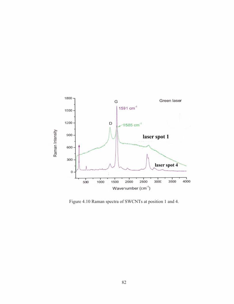
82
Figure 4.10 Raman spectra of SWCNTs at position 1 and 4.
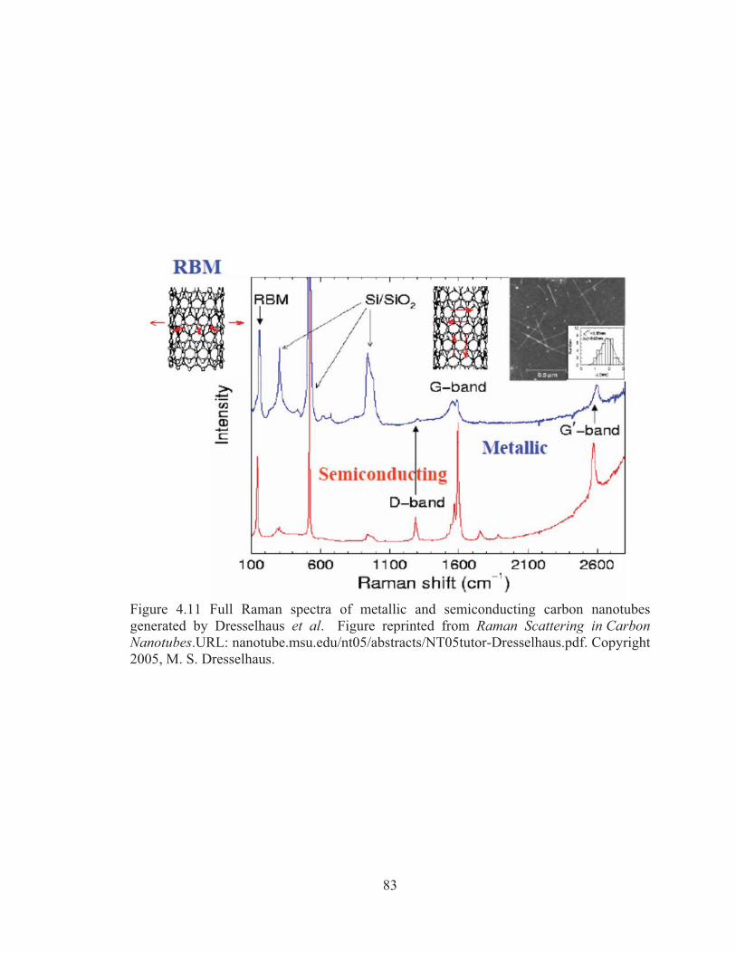
83
Figure 4.11 Full Raman spectra of metallic and semiconducting carbon nanotubes generated by Dresselhaus et al. Figure reprinted from Raman Scattering in Carbon Nanotubes.URL: nanotube.msu.edu/nt05/abstracts/NT05tutor-Dresselhaus.pdf. Copyright 2005, M. S. Dresselhaus.
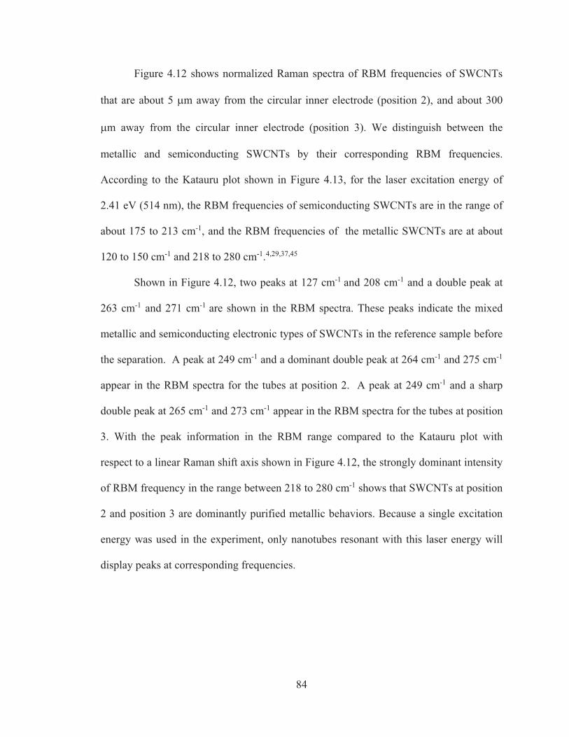
84
Figure 4.12 shows normalized Raman spectra of RBM frequencies of SWCNTs
that are about 5 �m away from the circular inner electrode (position 2), and about 300
�m away from the circular inner electrode (position 3). We distinguish between the
metallic and semiconducting SWCNTs by their corresponding RBM frequencies.
According to the Katauru plot shown in Figure 4.13, for the laser excitation energy of
2.41 eV (514 nm), the RBM frequencies of semiconducting SWCNTs are in the range of
about 175 to 213 cm-1, and the RBM frequencies of the metallic SWCNTs are at about
120 to 150 cm-1 and 218 to 280 cm-1.4,29,37,45
Shown in Figure 4.12, two peaks at 127 cm-1 and 208 cm-1 and a double peak at
263 cm-1 and 271 cm-1 are shown in the RBM spectra. These peaks indicate the mixed
metallic and semiconducting electronic types of SWCNTs in the reference sample before
the separation. A peak at 249 cm-1 and a dominant double peak at 264 cm-1 and 275 cm-1
appear in the RBM spectra for the tubes at position 2. A peak at 249 cm-1 and a sharp
double peak at 265 cm-1 and 273 cm-1 appear in the RBM spectra for the tubes at position
3. With the peak information in the RBM range compared to the Katauru plot with
respect to a linear Raman shift axis shown in Figure 4.12, the strongly dominant intensity
of RBM frequency in the range between 218 to 280 cm-1 shows that SWCNTs at position
2 and position 3 are dominantly purified metallic behaviors. Because a single excitation
energy was used in the experiment, only nanotubes resonant with this laser energy will
display peaks at corresponding frequencies.
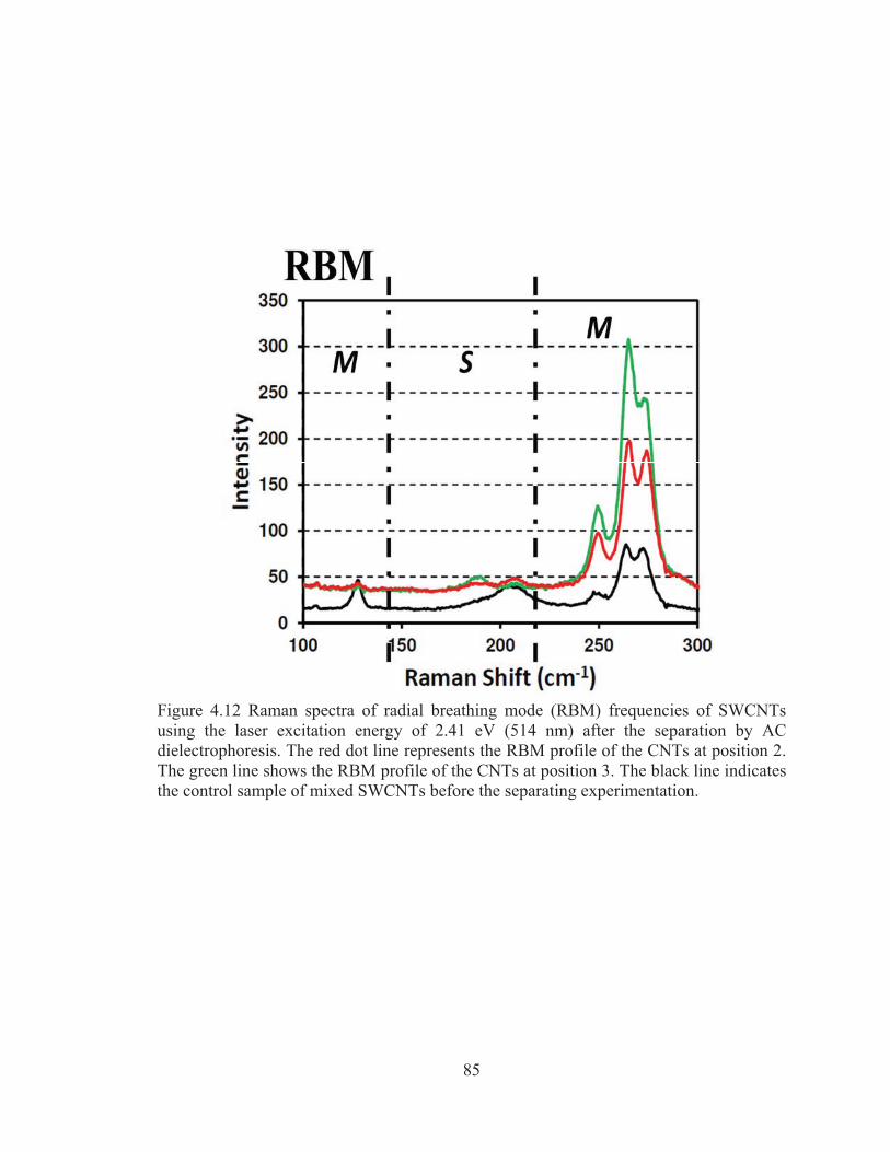
85
Figure 4.12 Raman spectra of radial breathing mode (RBM) frequencies of SWCNTs using the laser excitation energy of 2.41 eV (514 nm) after the separation by AC dielectrophoresis. The red dot line represents the RBM profile of the CNTs at position 2. The green line shows the RBM profile of the CNTs at position 3. The black line indicates the control sample of mixed SWCNTs before the separating experimentation.
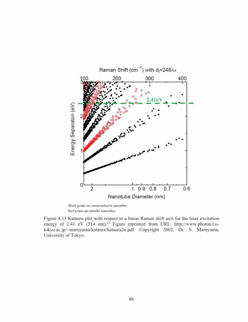
86
Figure 4.13 Katauru plot with respect to a linear Raman shift axis for the laser excitation energy of 2.41 eV (514 nm).22 Figure reprinted from URL: http://www.photon.t.u-tokyo.ac.jp/~maruyama/kataura/kataura2n.pdf. Copyright 2002, Dr. S. Maruyama, University of Tokyo.
2.41eV
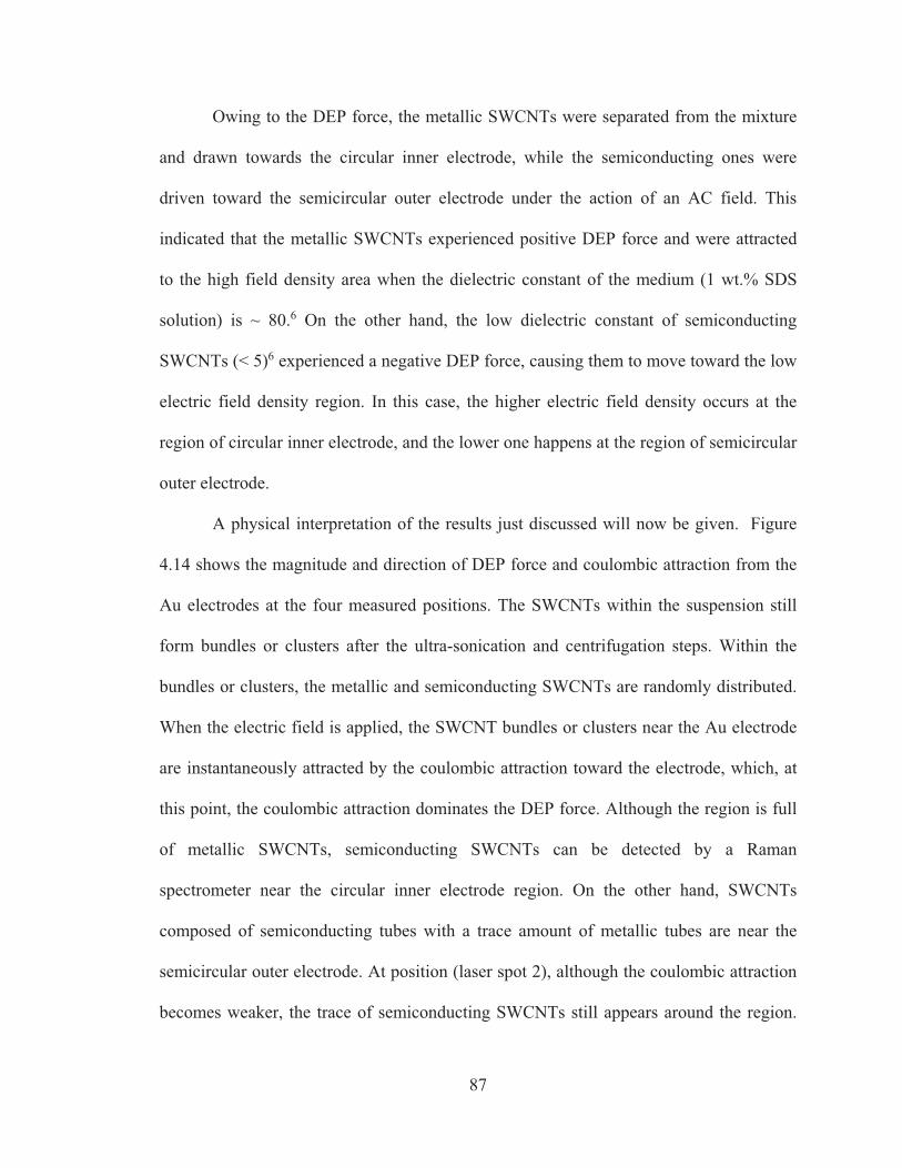
87
Owing to the DEP force, the metallic SWCNTs were separated from the mixture
and drawn towards the circular inner electrode, while the semiconducting ones were
driven toward the semicircular outer electrode under the action of an AC field. This
indicated that the metallic SWCNTs experienced positive DEP force and were attracted
to the high field density area when the dielectric constant of the medium (1 wt.% SDS
solution) is ~ 80.6 On the other hand, the low dielectric constant of semiconducting
SWCNTs (< 5)6 experienced a negative DEP force, causing them to move toward the low
electric field density region. In this case, the higher electric field density occurs at the
region of circular inner electrode, and the lower one happens at the region of semicircular
outer electrode.
A physical interpretation of the results just discussed will now be given. Figure
4.14 shows the magnitude and direction of DEP force and coulombic attraction from the
Au electrodes at the four measured positions. The SWCNTs within the suspension still
form bundles or clusters after the ultra-sonication and centrifugation steps. Within the
bundles or clusters, the metallic and semiconducting SWCNTs are randomly distributed.
When the electric field is applied, the SWCNT bundles or clusters near the Au electrode
are instantaneously attracted by the coulombic attraction toward the electrode, which, at
this point, the coulombic attraction dominates the DEP force. Although the region is full
of metallic SWCNTs, semiconducting SWCNTs can be detected by a Raman
spectrometer near the circular inner electrode region. On the other hand, SWCNTs
composed of semiconducting tubes with a trace amount of metallic tubes are near the
semicircular outer electrode. At position (laser spot 2), although the coulombic attraction
becomes weaker, the trace of semiconducting SWCNTs still appears around the region.
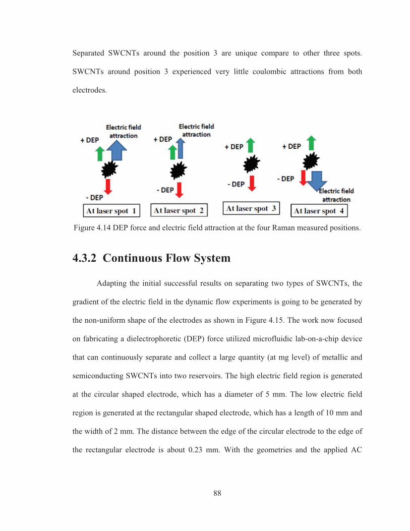
88
Separated SWCNTs around the position 3 are unique compare to other three spots.
SWCNTs around position 3 experienced very little coulombic attractions from both
electrodes.
Figure 4.14 DEP force and electric field attraction at the four Raman measured positions.
4.3.2 Continuous Flow System
Adapting the initial successful results on separating two types of SWCNTs, the
gradient of the electric field in the dynamic flow experiments is going to be generated by
the non-uniform shape of the electrodes as shown in Figure 4.15. The work now focused
on fabricating a dielectrophoretic (DEP) force utilized microfluidic lab-on-a-chip device
that can continuously separate and collect a large quantity (at mg level) of metallic and
semiconducting SWCNTs into two reservoirs. The high electric field region is generated
at the circular shaped electrode, which has a diameter of 5 mm. The low electric field
region is generated at the rectangular shaped electrode, which has a length of 10 mm and
the width of 2 mm. The distance between the edge of the circular electrode to the edge of
the rectangular electrode is about 0.23 mm. With the geometries and the applied AC
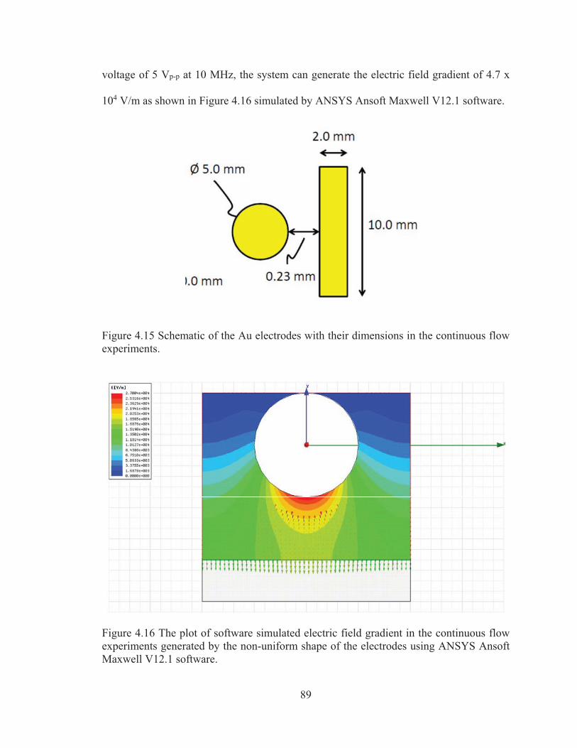
89
voltage of 5 Vp-p at 10 MHz, the system can generate the electric field gradient of 4.7 x
104 V/m as shown in Figure 4.16 simulated by ANSYS Ansoft Maxwell V12.1 software.
Figure 4.15 Schematic of the Au electrodes with their dimensions in the continuous flow experiments.
Figure 4.16 The plot of software simulated electric field gradient in the continuous flow experiments generated by the non-uniform shape of the electrodes using ANSYS Ansoft Maxwell V12.1 software.
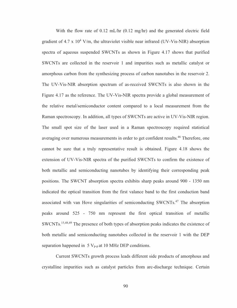
90
With the flow rate of 0.12 mL/hr (0.12 mg/hr) and the generated electric field
gradient of 4.7 x 10⁴ V/m, the ultraviolet visible near infrared (UV-Vis-NIR) absorption
spectra of aqueous suspended SWCNTs as shown in Figure 4.17 shows that purified
SWCNTs are collected in the reservoir 1 and impurities such as metallic catalyst or
amorphous carbon from the synthesizing process of carbon nanotubes in the reservoir 2.
The UV-Vis-NIR absorption spectrum of as-received SWCNTs is also shown in the
Figure 4.17 as the reference. The UV-Vis-NIR spectra provide a global measurement of
the relative metal/semiconductor content compared to a local measurement from the
Raman spectroscopy. In addition, all types of SWCNTs are active in UV-Vis-NIR region.
The small spot size of the laser used in a Raman spectroscopy required statistical
averaging over numerous measurements in order to get confident results.46 Therefore, one
cannot be sure that a truly representative result is obtained. Figure 4.18 shows the
extension of UV-Vis-NIR spectra of the purified SWCNTs to confirm the existence of
both metallic and semiconducting nanotubes by identifying their corresponding peak
positions. The SWCNT absorption spectra exhibits sharp peaks around 900 - 1350 nm
indicated the optical transition from the first valance band to the first conduction band
associated with van Hove singularities of semiconducting SWCNTs.47 The absorption
peaks around 525 - 750 nm represent the first optical transition of metallic
SWCNTs.15,48,49 The presence of both types of absorption peaks indicates the existence of
both metallic and semiconducting nanotubes collected in the reservoir 1 with the DEP
separation happened in 5 Vp-p at 10 MHz DEP conditions.
Current SWCNTs growth process leads different side products of amorphous and
crystalline impurities such as catalyst particles from arc-discharge technique. Certain
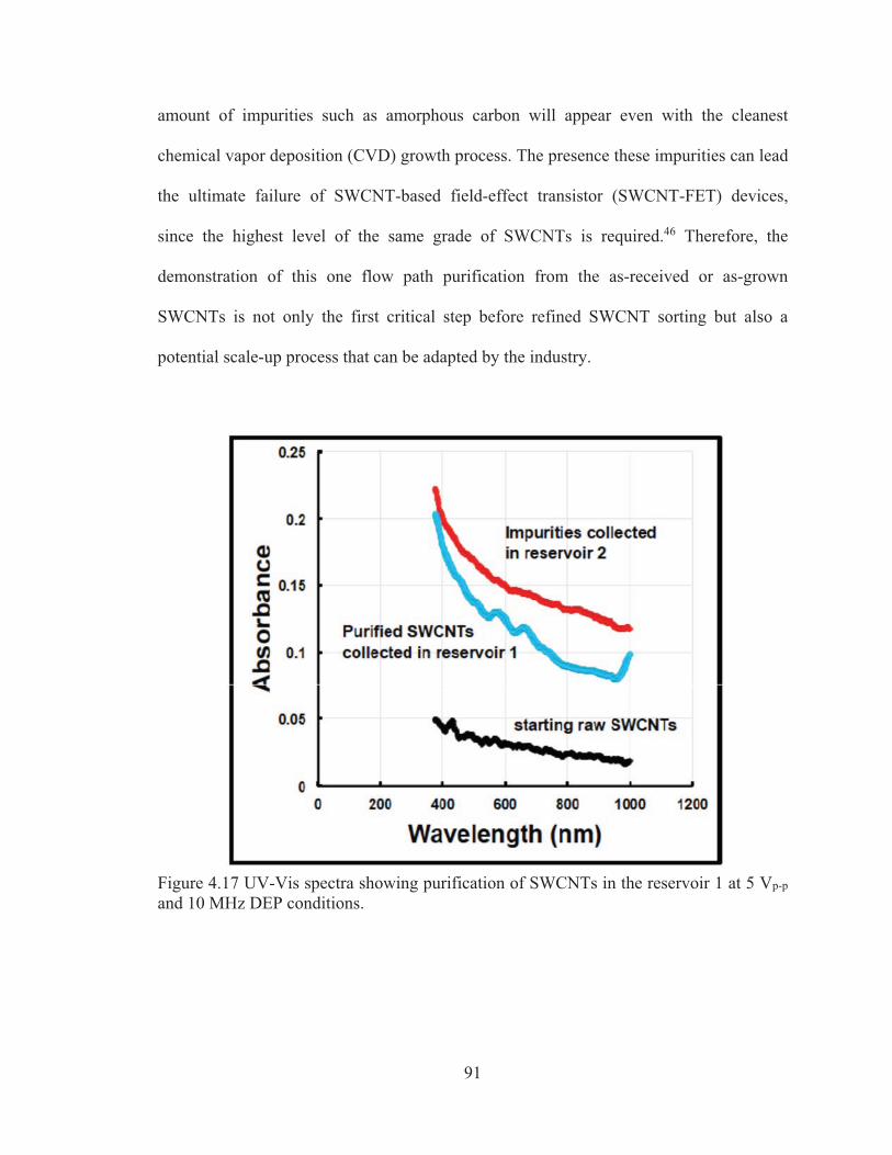
91
amount of impurities such as amorphous carbon will appear even with the cleanest
chemical vapor deposition (CVD) growth process. The presence these impurities can lead
the ultimate failure of SWCNT-based field-effect transistor (SWCNT-FET) devices,
since the highest level of the same grade of SWCNTs is required.46 Therefore, the
demonstration of this one flow path purification from the as-received or as-grown
SWCNTs is not only the first critical step before refined SWCNT sorting but also a
potential scale-up process that can be adapted by the industry.
Figure 4.17 UV-Vis spectra showing purification of SWCNTs in the reservoir 1 at 5 Vp-p
and 10 MHz DEP conditions.
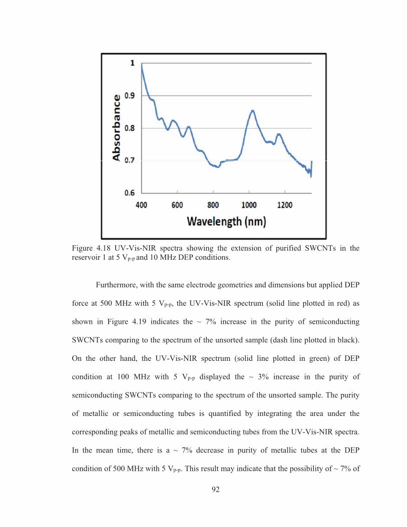
92
Figure 4.18 UV-Vis-NIR spectra showing the extension of purified SWCNTs in the reservoir 1 at 5 Vp-p and 10 MHz DEP conditions.
Furthermore, with the same electrode geometries and dimensions but applied DEP
force at 500 MHz with 5 Vp-p, the UV-Vis-NIR spectrum (solid line plotted in red) as
shown in Figure 4.19 indicates the ~ 7% increase in the purity of semiconducting
SWCNTs comparing to the spectrum of the unsorted sample (dash line plotted in black).
On the other hand, the UV-Vis-NIR spectrum (solid line plotted in green) of DEP
condition at 100 MHz with 5 Vp-p displayed the ~ 3% increase in the purity of
semiconducting SWCNTs comparing to the spectrum of the unsorted sample. The purity
of metallic or semiconducting tubes is quantified by integrating the area under the
corresponding peaks of metallic and semiconducting tubes from the UV-Vis-NIR spectra.
In the mean time, there is a ~ 7% decrease in purity of metallic tubes at the DEP
condition of 500 MHz with 5 Vp-p. This result may indicate that the possibility of ~ 7% of
93
metallic nanotubes trapped and attracted on the Au electrode by the stronger DEP force
due to the larger electric field gradient while much pure semiconducting nanotubes are
pushed into the reservoir by the flow. The absorptivities of as-received and unsorted
SWCNTs are tested by the in-house UV-Vis-NIR spectroscopy to ensure the accuracy of
the purity measurement. The absorptivities of unsorted tubes were 27.8% and 72.2%,
respectively. The theoretical concentrations of metallic and semiconducting SWCNTs are
about 33% and 67%, respectively.47 Therefore, the good match between the measured
data and the theoretical prediction indicates the reliability of the SWCNT purity
measurement.
Figure 4.19 UV-Vis-NIR spectrum showing indicates the ~ 7% increase in purity of semiconducting SWCNTs in both reservoirs at the DEP of (5 Vp-p, 500 MHz) and (5 Vp-p, 100 MHz) conditions.
94
4.4 Conclusions
The method to separate metallic from semiconducting SWCNTs in suspension
containing both types based on AC dielectrophoresis (DEP), was reported. Applying this
technique in a static system, metallic SWCNTs were effectively separated from
semiconducting ones due the different magnitude of dielectrophoretic forces experienced
in the suspension between these two types. The significant force difference comes from a
very large absolute dielectric constant of metallic SWCNTs and the low value of a finite
dielectric constant of semiconducting nanotubes. It was discovered that the repulsive
effect between positive and negative DEP forces is the strongest in the center portion
between the circular inner electrode and semicircular outer electrode. Resonant Raman
spectroscopy was used to confirm the observed results. In the dynamic flow system, the
feasibility of continuously collecting purified SWCNTs with the designed flow device at
10 MHz and 5 Vp-p DEP conditions is demonstrated by confirming the UV-Vis-NIR
spectra. Moreover, the experiment also demonstrates the feasibility of continuously
collecting refined semiconducting SWCNTs with the same flow device at (500 MHz, 5
Vp-p) and (100 MHz, 5 Vp-p) DEP conditions.
95
4.5 Future Work
With these successful initial results, we have demonstrated that SWCNTs
purification and sorting in a single pass flow system is possible. Some avenues to
enhance the refinement of metallic or semiconducting SWCNTs are to optimize the flow
and separation parameters. For collecting more refined semiconducting SWCNTs, the
geometry of electrode could be optimized in order to create a greater electric field
gradient and therefore greater DEP force. A tip shaped electrode could be substituted for
the circular shaped electrode, thus enhancing the DEP force acting on the metallic tubes.
As a result, more metallic nanotubes would be attracted towards the tip-shaped
electrode. Therefore, a significantly greater quantity of more refined semiconducting
SWCNTs could be collected in the reservoirs. Another possibility is to collect refined
metallic nanotubes by adding a channel of buffer (SWCNT-free) solution at the same
constant flow rate as the mixed SWCNTs suspension in order to flush the metallic
SWCNTs attached on the electrode, thus improve the purity of metallic SWCNTs
collected in the reservoirs. The image of an extra buffer channeled prototype was built
and is shown in Figure 4.20.
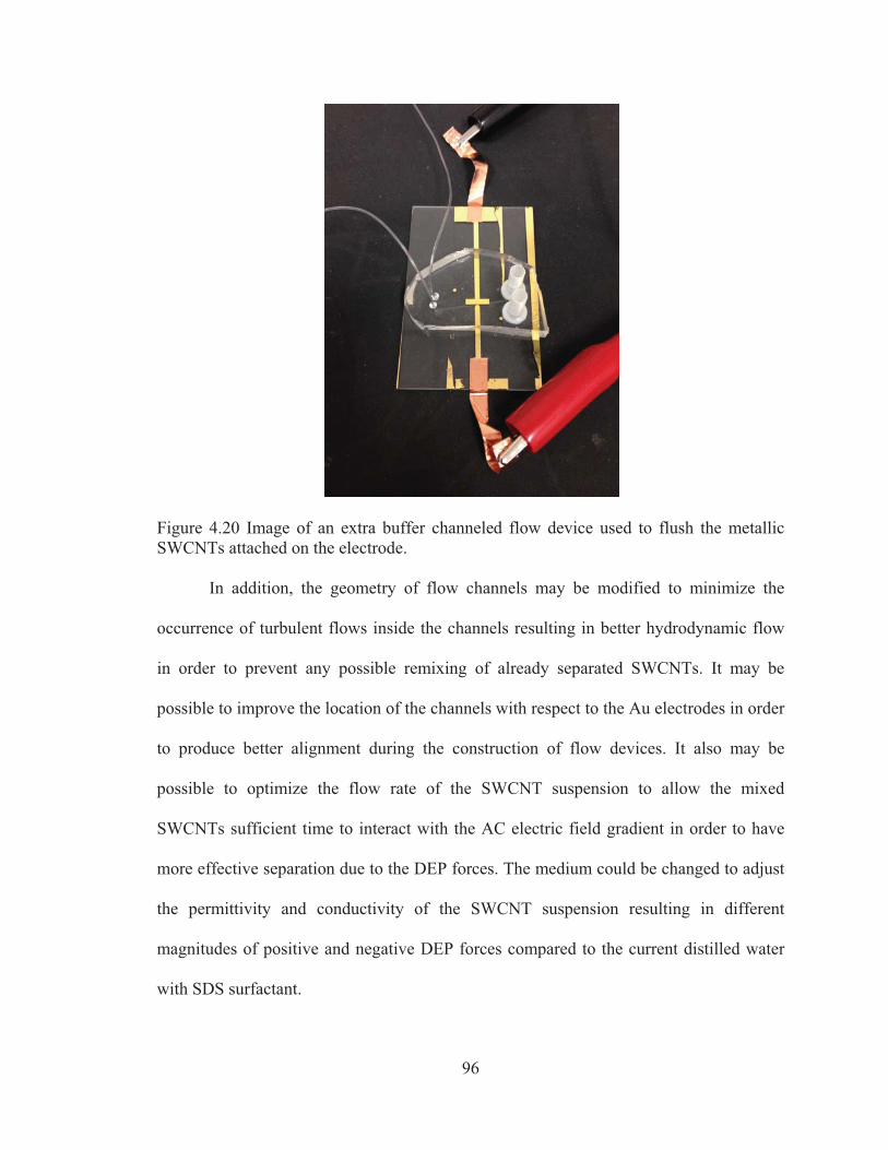
96
Figure 4.20 Image of an extra buffer channeled flow device used to flush the metallic SWCNTs attached on the electrode. In addition, the geometry of flow channels may be modified to minimize the
occurrence of turbulent flows inside the channels resulting in better hydrodynamic flow
in order to prevent any possible remixing of already separated SWCNTs. It may be
possible to improve the location of the channels with respect to the Au electrodes in order
to produce better alignment during the construction of flow devices. It also may be
possible to optimize the flow rate of the SWCNT suspension to allow the mixed
SWCNTs sufficient time to interact with the AC electric field gradient in order to have
more effective separation due to the DEP forces. The medium could be changed to adjust
the permittivity and conductivity of the SWCNT suspension resulting in different
magnitudes of positive and negative DEP forces compared to the current distilled water
with SDS surfactant.
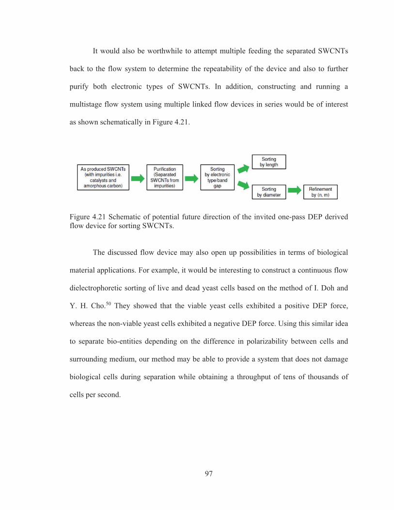
97
It would also be worthwhile to attempt multiple feeding the separated SWCNTs
back to the flow system to determine the repeatability of the device and also to further
purify both electronic types of SWCNTs. In addition, constructing and running a
multistage flow system using multiple linked flow devices in series would be of interest
as shown schematically in Figure 4.21.
Figure 4.21 Schematic of potential future direction of the invited one-pass DEP derived flow device for sorting SWCNTs.
The discussed flow device may also open up possibilities in terms of biological
material applications. For example, it would be interesting to construct a continuous flow
dielectrophoretic sorting of live and dead yeast cells based on the method of I. Doh and
Y. H. Cho.50 They showed that the viable yeast cells exhibited a positive DEP force,
whereas the non-viable yeast cells exhibited a negative DEP force. Using this similar idea
to separate bio-entities depending on the difference in polarizability between cells and
surrounding medium, our method may be able to provide a system that does not damage
biological cells during separation while obtaining a throughput of tens of thousands of
cells per second.
98
Bibliography
1. P. Avouris, Feature: Nanotube electronics, Physics World 20, 40-45 (2007).
2. P. Avouris and J. Appenzeller, Electronics and Optoelectronics with Carbon
Nanotubes, The Industrial Physicist, June/July, 18-21 (2004).
3. M. John, Exotic Carbon Molecules Offer a Promising Path To Ever Smaller
Chips, page B2, New York edition, The New York Times (October 29th, 2012).
URL: http://bits.blogs.nytimes.com/2012/10/28/i-b-m-reports-nanotube-chip-
breakthrough/?_r=0
4. R. Krupke, F. Hennrich, H. v. Löhneysen, and M. M. Kappes, Separation of
Metallic from Semiconducting Single-Walled Carbon Nanotubes, Science 301,
344-347 (2003).
5. N. Peng, Q. Zhang, J. Li, and N. Liu, Influences of ac electric field on the spatial
distribution of carbon nanotubes formed between electrodes, J. Appl. Phys. 100,
024309 (2006).
6. R. Krupke, F. Hennrich, M. M. Kappes, and H. v. Löhneysen, Surface
Conductance Induced Dielectrophoresis of Semiconducting Single-Walled
Carbon Nanotubes, Nano. Lett. 3, 1019-1023 (2003).
7. T. Tanaka, H. Jin, Y. Miyata, and H. Kataura, High-Yield Separation of Metallic
and Semiconducting Single-Wall Carbon Nanotubes by Agarose Gel
Electrophoresis, Appl. Phys. Expr. 1, 114001 (2008).
8. Price of sorted metallic and semiconducting nanotubes.
URL:http://www.sigmaaldrich.com/technical-documents/articles/materials-
science/nanointegris.html
99
9. M. S. Dresselhaus, G. Dresselhaus, and M. Pimenta, The remarkable properties of
carbon nanotubes as nanoclusters, Eur. Phys. J. D. 9, 69-75 (1999).
10. M. S. Dresselhaus, G. Dresselhaus, A. Jorio, A. G. Souza Filho, and R. Saito,
Raman spectroscopy on isolated single wall carbon nanotubes, Carbon 40, 2043-
2061 (2002).
11. P. Avouris, J. Appenzeller, R. Martel, and S. J. Wind, Carbon Nanotube
Electronics, Proceedings of the IEEE 91 (11), 1772-1784 (2003).
12. This section is an adapted reproduction from Su Chih Chi, Robert C. Cammarata,
Chia-Ling Chien, Donglei Fan, Stephen Farias, and Danru Qu, inventors, Johns
Hopkins University, assignee, “Systems and Methods for Separating Metallic and
Nonmetallic Particles in a Mixed-Particle Suspension,” U. S. Patent Provisional
Application No. 13/902,191, Filling date: May 24, 2013.
13. M. S. Dresselhaus, G. Dresselhaus, and R. Saito, PHYSICS OF CARBON
NANOTUBES, Carbon 33, 883-891 (1995).
14. M. Ouyang, J.-L. Huang, and C. M. Lieber, Fundamental Electronic Properties
and Applications of Single-Walled Carbon Nanotubes, Acc. Chem. Res. 35 (12),
1018-1025 (2002).
15. H. Liu, Y. Feng, T. Tanaka, Y. Urabe, and H. Kataura, Diameter-Selective
Metal/Semiconductor Separation of Single-wall Carbon Nanotubes by Agarose
Gel, J. Phys. Chem. C 114, 9270-9276 (2010).
16. M. S. Dresselhaus, G. Dresselhaus, R. Saito, A. Jorio, Raman spectroscopy of
carbon nanotubes, Physics Reports 409, 47-99 (2005).

100
17. E. Pop, D, Mann, Q. Wang, K. Goodson, and H Dai, Thermal Conductance of an
Individual Single-Walled Carbon Nanotube above Room Temperature, Nano.
Lett. 6 (1), 96-100 (2006).
18. S. Sinha, S. Barjami, G. Iannacchione, A. Schwab, and G. Muench, Off-axis
Thermal Properties of Carbon Nanotube Films, Journal of Nanoparticle
Research, Vol. 7, Issue 6, pp 651-657 (2005).
19. S. Frank, P. Poncharal, Z. L. Wang, and W. A. deHeer, Carbon nanotube quantum
resistors, Science 280, 1744-1746 (1998).
20. K. Moshammer, F. Hennrich, and M. M. Kappes, Selective suspension in
aqueous sodium dodecyl sulfate according to electronic structure type allows
simple separation of metallic from semiconducting single-walled carbon
nanotubes, Nano Research 2 (8), pp 599-606 (2009).
21. M. S. Dresselhaus, Carbon Nanotubes: Synthesis, Structure, Properties, and
Applications. Springer (2001).
22. U. C. Wejinya, N. Xi, Y. Shen, and K. W. C. Lai, Modeling Dielectrophoretic
Force for Manipulating Carbon Nanotubes (CNTs), 2007 IEEE/ASME
International Conference on Advanced Intelligent Mechatronics. pp 1-6 (2007).
23. H. Morgan and N. G. Green, J. Electrostatics 42, 279-293 (1997).
24. H. Morgan and N. G. Green, AC Electrokinetics: Colloids and Nanoparticels,
Research Studies Press Ltd, 2003.
25. J. E. Kim and C. S. Han, Use of dielectrophoresis in the fabrication of an atomic
force microscope tip with a carbon nanotube: a numerical analysis,
Nanotechnology 16, 2245-2250 (2005).
101
26. H. A. Pohl, Dielectrophoretic, Cambridge, UK (1978).
27. T. Lutz and K. J. Donovan, Macroscopic scale separation of metallic and
semiconducting nanotubes by dielectrophoresis, Carbon 43, 2508-2513 (2005).
28. C. Wei, T.-Y. Wei, and F.-C. Tai, The characteristics of multi-walled carbon
nanotubes by a two-step separation scheme via dielectrophoresis, Diamonds and
Related Materials 19, 573-577 (2010).
29. D. S. Lee D. W. Kim, H. S. Kim. S. W. Lee, S. H. Jhang, Y. W. Park, and E. E. B.
Campbell, Extraction of semiconducting CNTs by repeated dielectrophoretic
filtering, Appl. Phys. A 80, 5-8 (2005).
30. H. K. Schmidt, H. Peng, M. J. Mends, and M. Pasquali, Flow Dielectrophoretic
Separation of Single Wall Carbon Nanotubes, United States Patent Application
Publication, Pub. No.: US2009/0283405 A1, Pub. Date: Nov. 19, 2009.
31. A. Jorio, R. Saito, J. H. Hafner, C. M. Lieber, M. Hunter, T. McClure, G.
Dresselhaus, and M. S. Dresselhaus, Structural (n, m) Determination of Isolated
Single-Wall Carbon Nanotubes by Resonant Raman Scattering, Phys. Rev. Lett.
86 (6), 1118-1121 (2001).
32. M. S. Dresselhaus and P. C. Eklund, Phonons in carbon nanotubes, Adv. Phys. 49
(6), 705-814 (2000).
33. P. T. Araujo, A. Jorio, M. S. Dresselhaus, K. Sato, and R. Saito, Diameter
Dependence of the Dielectric Constant for the Excitonic Transition Energy of
Single-Wall Carbon Nanotubes, Phys. Rev. Lett. 103, 146802 (2009).
34. P. T. Araujo, O. Maciel, P. B. C. Pesce, M. A. Pimenta, S. K. Doorn, H. Qian, A.
Hartschuh, M. Steiner, L. Grigorian, K. Hata, and A. Jorio, Nature of the constant
102
factor in the relation between radial breathing mode frequency and tube diameter
for single-walled carbon nanotubes, Phys. Rev. B 77, 241403(R) (2008).
35. S. M. Bachilo, M. S. Strano, C. Kittrell, R. H. Hauge, R. E. Smalley, and R. B.
Weisman, Structure-Assigned Optical Spectra of Single-Walled Carbon
Nanotubes, Science 298, 2361-2366 (2002).
36. S. Costa, E. Borowiak-Palen, M. Kruszy�ska, A. Bachmatiuk, and R. J.
Kale�czuk, Characterization of Carbon Nanotubes by Raman Spectroscopy,
Materials Science-Poland 26(2), 433-441 (2008).
37. J. L. Sauvajol, E. Anglaret, S. Rols, and L. Alvarez, Phonons in single wall
carbon nanotube bundles, Carbon 40, 1697-1714 (2002).
38. I. L. Li, G. D. Li, H. J. Liu, C. T. Chan, and Z. K. Tang, Chirality-dependent
curvature effect in smallest single-walled carbon nanotubes, Appl. Phys. Lett. 82,
1467 (2003).
39. D. Sánchez-Portal, E. Artacho, J. M. Soler, A. Rubio, and P. Ordejón,
Characterization methods of carbon nanotubes, Phys. Rev. B 59, 12768 (1999).
40. M. S. Dresselhaus, Raman Scattering in Carbon Nanotubes (2005).
URL: nanotube.msu.edu/nt05/abstracts/NT05tutor-Dresselhaus.pdf
41. M. A. Pimenta, A. Marucci, S. A. Empedocles, M. G. Bawendi, E. B. Hanlon, A.
M. Rao, P. C. Eklund, R. E. Smalley, G. Dresselhaus, and M. S. Dresselhaus,
Raman modes of metallic carbon nanotubes, Phys. Rev. B 58, R16016-16019
(1998).
103
42. S. K. Doorn, M. J. O’Connell, L. Zheng, Y. T. Zhu, S. Huang, and J. Liu, Raman
Spectral Imaging of a Carbon Nanotube Intramolecular Junction, Phys. Rev, Lett.
94, 016802 (2005).
43. H. Kuzmany, B. Burger, A. Thess, and R. E. Smalley, Vibrational spectra of
single wall carbon nanotubes, Carbon 36(5-6), 709-712 (1998).
44. H. Kataura, Y. Kumazawa, Y. Maniwa, I. Umezu, S. Suzuki, Y. Ohtsuka, and Y.
Achiba, optical Properties of Single-Wall Carbon Nanotubes, Synthetic Metals
103, 2555-2558 (1999).
45. Katauru plot with respect to a linear Raman shift axis. URL:
http://www.photon.t.u-tokyo.ac.jp/~maruyama/kataura/kataura2n.pdf
46. P. Chaturvedi, P. Verma, A, Singh, P. K. Chaudhary, H. Basu, and P. K. Basu,
Carbon Nanotube-Purification and Sorting Protocols, Defence Science Journal
58(5), 591-599 (2008).
47. M. S. Strano, C. A. Dyke, M. L. Usrey, P. W. Barone, M. J. Allen, H. Shan, C.
Kittrell, R. H. Hauge, J. M. Tour, R. E. Smalley, Electronic Structure Control of
Single-Walled Carbon Nanotube Functionalization, Science 301(5639), 1519-
1522 (2003).
48. M. S. Strano, Probing chiral selective reactions using a revised Kataura plot for
the interpretation of single-walled carbon nanotube spectroscopy, J. Am. Chem.
Soc. 125, 16148-16153 (2003).
49. M. S. Arnold, A. A. Green J. F. Hulvat, S. I. Stupp, and M. C. Hersam, Sorting
carbon nanotubes by electronic structure using density differentiation, Nature
Nanotechnology 1, 60-65 (2006).

104
50. I. Doh and Y. H. Cho, A continuous cell separation chip using hydrodynamic
dielectrophoresis (DEP) process, Sensors and Actuators A 121, 59-65 (2005).
105
Chapter 5
Summary
In this Final chapter, the author would like to summarize the previous discussions.
In the first chapter, the author described the feasibility of electrodepositing pure
lanthanum and lanthanum telluride compounds in ambient conditions are demonstrated.
Scanning electron microscope (SEM) images showed that surface morphologies of the
deposited films varied from needle-like to granular structures depending on the
deposition conditions. Many nanostructured surface features on the electrodeposited
samples may enhance ZT because the appearance of a large numbers of grain boundaries
can scatter phonons more effectively than electrons resulting in a lowering of the thermal
conductivity. The measured Seebeck coefficients and electrical resistivity of the
electrodeposited thin films were closely matched to the state-of-the-art thermoelectric
properties of bulk samples synthesized by mechanical alloying and the hot-press
sintering. The calculated power factor of the deposited films was ranged from 8.1 x 10⁻⁵
to 28.5 x 10⁻⁵ (W m-1 K-2). The X-ray diffraction pattern and the energy dispersive X-ray
(EDAX) composition analysis of electrodeposited La3-xTe4 films indicated that the
samples are phase pure materials.
In the second chapter, the author has shown using electrodeposition to fabricate
vertically-aligned gold nanowires on a gold substrate. Scanning electron microscope
(SEM) images show the gold nanowire arrays were highly dense and strongly attached to
106
the gold substrate after dissolution of the nanoporous anodic aluminum oxide (AAO)
template. Gold nanowire arrays ferromagnetic composite films were synthesized for the
first time by evaporation or electrodeposition to embed gold nanowires in nickel matrices
and by electrodeposition to grow iron matrices around the gold nanowires. The
electrodeposition technique preserved the spacing of the exposed gold nanowires better
than the electron beam evaporation technique does. For both techniques, the density of
gold nanowires across the nickel and iron matrices was homogenous regardless of the
fabrication parameters.
In Chapter 3, the author has presented a novel and relatively simple approach for
the synthesis of nanochanneled metal membranes with different pore sizes and inter-pore
distance. Nickel nanoporous membranes of thickness less than about 0.7 �m were
produced by physical vapor deposition of nickel overlayers by either electron beam
evaporation or sputtering onto anodic aluminum oxide nanoporous substrates with
vertically aligned nanochannels. The resulting overlayers were nanoporous, with the
nanopores in the form of nanochannels aligned with the nanochannels of the substrate. In
the case of the evaporated membranes, the pores had diameters within a factor of 2.5 of
that of the substrate (100 nm) and a similar planar density, suggesting that the substrate
acted as a template for the nanoporous nickel. The sputtered nickel also was deposited as
a nanoporous material, but with a greater density of pores and smaller pore diameters,
suggesting partial filling and incomplete agglomeration within the initially formed pores.
For sputtered overlayers of thickness 0.7 �m or greater, the deposited metal became
continuous, and electrochemical etching through the nanoporous anodic aluminum oxide
(AAO) substrate was used to on these samples to produce the nanochannels. For all of
107
the samples, the substrate could be completely dissolved, resulting in free-standing
metallic membranes.
In the fourth chapter, the author has reported a patented microfluidic device that
can continuously purify and refine mixed electronic types of single-walled carbon
nanotubes (SWCNTs) into separated reservoirs of metallic SWCNTs and semiconducting
ones, respectively. Based on AC dielectrophoresis (DEP) in a static system, metallic
SWCNTs are effectively separated from semiconducting ones due the different
magnitude of dielectrophoretic forces experienced in the suspension between these two
types. The significant force difference comes from a very large absolute dielectric
constant of metallic CNTs and the low value of a finite dielectric constant of
semiconducting nanotubes. It is discovered that the repulsive effect between positive and
negative DEP forces is the strongest in the center portion between the circular inner
electrode and semicircular outer electrode. Resonant Raman spectroscopy is used to
confirm the observed results. In the dynamic flow system, the feasibility of continuously
collecting purified SWCNTs with the designed flow device at 10 MHz and 5 Vp-p DEP
conditions is demonstrated by confirming the UV-Vis-NIR spectra. Moreover, the
experiment also demonstrates the feasibility of continuously collecting refined
semiconducting SWCNTs with the same flow device at 500 MHz and 2 Vp-p DEP
conditions.
108
A List of Publications and Patents
1. Su Chih Chi, Stephen L. Farias, and Robert C. Cammarata, “Synthesis of Vertically
Aligned Gold Nanowire-Ferromagnetic Metal Matrix Composites” ECS
Trans. 2012 41(35): 119-122; doi: 10.1149/1.3699386.
2. Su (Ike) Chih Chi, Stephen L. Farias, and Robert C. Cammarata, “Fabrication of
Lanthanum Telluride Thin Films Electrochemical Deposition in Ambient
Conditions,” Mater. Res. Soc. Symp. Proc. Vol. 1543 (2013).
3. Su Chih Chi, Robert C. Cammarata, Chia-Ling Chien, Donglei Fan, Stephen Farias,
and Danru Qu, inventors, Johns Hopkins University, assignee, “Systems and Methods
for Separating Metallic and Nonmetallic Particles in a Mixed-Particle Suspension,”
U. S. Patent Provisional Application No. 13/902,191, Filling date: May 24, 2013.
109
A List of Conference Presentations and Poster Sessions
1. Su (Ike) Chih Chi, Stephen L. Farias, and Robert C. Cammarata, A Novel Approach
to Synthesize Lanthanum Telluride Thermoelectric Materials, Materials Research
Society Fall Meeting, Boston, MA USA, December 3, 2013.
2. Su (Ike) Chih Chi, Stephen L. Farias, and Robert C. Cammarata, A Novel Approach
to Synthesize Lanthanum Telluride Thermoelectric Materials in Ambient Conditions,
Materials Research Society Spring Meeting, San Francisco, CA USA, April 3, 2013.
3. Su (Ike) Chih Chi, Stephen L. Farias, and Robert C. Cammarata, APS March
Meeting, A Novel Approach to Synthesize Lanthanum Telluride Thermoelectric Thin
Films in Ambient Conditions, Baltimore, MD USA, March 21, 2013.
4. Su (Ike) Chih Chi, Xuan Jiang, Danru Qu, Stephen L. Farias, SunXiang Huang, Deng
Pan, C. L. Chien, Hai-Quan Mao, and Robert C. Cammarata, Precise Manipulation of
Gold Nanowires as Gene Delivery Vehicles, Materials Research Society Fall
Meeting, Boston, MA USA, November 29, 2011.
5. Su (Ike) Chih Chi, Stephen L. Farias, Konrad Bussmann, Joshua D. Caldwell, Danru
Qu, Mingen Li, C. L. Chien, and Robert C. Cammarata, Synthesis and Magnetic
Properties of Ordered, Vertically-Aligned Au Nanowire Composites and
Ferromagnetic Nanochanneled Membranes, 220th Electrochemical Society Meeting,
Boston, MA USA, October 10, 2011.
6. Su (Ike) Chih Chi, SunXiang Huang, Danru Qu, Nicholas Dee, Korey Kam, XingYu
Liu, C. L. Chien, Hai-Quan Mao, and Robert C. Cammarata, Precise Manipulation of

110
Nanowires as Delivery Vehicles in Cellular Environments, Institute for NanoBio
Technology Annual Symposium Poster Session, Baltimore, MD USA, May 2011.