Embed Size (px)
Citation preview
Lead Lanthanum Zirconate Titanate Ceramic Thin Films for EnergyStorageSheng Tong,*,† Beihai Ma,‡ Manoj Narayanan,‡ Shanshan Liu,‡ Rachel Koritala,§
Uthamalingam Balachandran,‡ and Donglu Shi†
†College of Engineering and Applied Science, University of Cincinnati, Cincinnati, Ohio 45221, United States‡Energy Systems Division and §Nanoscience and Technology Division, Argonne National Laboratory, Argonne, Illinois 60439, UnitedStates
ABSTRACT: An acetic-acid-based sol−gel method was usedto deposit lead lanthanum zirconate titanate (PLZT, 8/52/48)thin films on either platinized silicon (Pt/Si) or nickel bufferedby a lanthanum nickel oxide buffer layer (LNO/Ni). X-raydiffraction and scanning electron microscopy of the samplesrevealed that dense polycrystalline PLZT thin films formedwithout apparent defects or secondary phases. The dielectricbreakdown strength was greater in PLZT thin films depositedon LNO/Ni compared with those on Pt/Si, leading to betterenergy storage. Finally, optimized dielectric properties weredetermined for a 3-μm-thick PLZT/LNO/Ni capacitor forenergy storage purposes: DC dielectric breakdown strength of ∼1.6 MV/cm (480 V), energy density of ∼22 J/cc, energy storageefficiency of ∼77%, and permittivity of ∼1100. These values are very stable from room temperature to 150 °C, indicating thatcost-effective, volumetrically efficient capacitors can be fabricated for high-power energy storage.
KEYWORDS: PLZT, energy storage, thin film, capacitor, relaxor ferroelectric, base metal substrate
■ INTRODUCTION
Because of climate change and global air pollution, intenseeffort is underway to replace high-CO2-emission fossil fuelenergy resources with cleaner renewable energy sources, suchas solar and wind energy technology, as well as hybrid electricvehicles. For the purpose of stationary energy storage andvehicle propulsion, the demand for high efficient electric energystorage is on the rise. Broadly, there are two classes of energystorage: short term and long term.1−3 The former is usually inthe form of batteries, whereas the latter is usually in the form ofcapacitors, which are able to smooth out momentaryfluctuations and ensure a stable supply of energy fromrenewable sources. Having orders of magnitude higher electricpower density and cycle life compared with batteries, capacitorscan be used to prolong the lifetime of batteries and improve thereliability of electric systems in hybrid vehicles, meet peakpower needs in hybrid and electric vehicles, and keep internalcombustion engines operating at an optimized energyefficiency. Although the battery-capacitor system has alreadybeen adopted widely in hybrid vehicles, more attention is nowbeing directed toward improving overall performance whilereducing module size, weight, and cost. Some of the desiredimprovements include increasing energy density, decreasingelectrical and thermal losses, improving packaging, andimproving reliability and lifetime.3,4
At present, polymer and electrolyte capacitors are often usedfor high-power output applications because of their highbreakdown voltage and energy density. Advanced materials,
e.g., supercapacitors, are considered a promising candidate totake the place of the battery-capacitor systems. However, toincrease their reliability and energy efficiency, more advancedmaterials and techniques are required. Polymer capacitorsusually exhibit low permittivity and low mechanical toleranceand must be operated within a limited temperature range.Electrolyte capacitors usually operate at low pulse repetitionrate, suffer from voltage reversal, and have limited lifetime.Supercapacitors have low single-cell electric potential andpackaging limitations.1,5−7 By contrast, ceramic capacitorsexhibit superior mechanical and thermal properties andorders-of-magnitude higher permittivity, and are thus consid-ered the potential best candidate for the high-power energystorage application.8 Yet, in the form of bulk and thick films(e.g., traditional multilayer ceramic capacitors), mainly BaTiO3
ceramics, they are not able to withstand high electric fields,leading to a relatively low energy density.9,10 Fortunately, theimprovement of the circuit design for hybrid vehicles hasresulted in lower operation voltage, down to subkilovolt levels,and durations, up to milliseconds. It is now possible to producethin-film ferroelectric capacitors demonstrating many attractiveproperties, such as high capacitance, low remanent voltage, highbreakdown strength, and low package volume. To better
Received: December 5, 2012Accepted: February 4, 2013Published: February 4, 2013
Research Article
www.acsami.org
© 2013 American Chemical Society 1474 dx.doi.org/10.1021/am302985u | ACS Appl. Mater. Interfaces 2013, 5, 1474−1480
Dow
nloa
ded
by U
NIV
OF
CIN
CIN
NA
TI
on A
ugus
t 31,
201
5 | h
ttp://
pubs
.acs
.org
P
ublic
atio
n D
ate
(Web
): F
ebru
ary
18, 2
013
| doi
: 10.
1021
/am
3029
85u
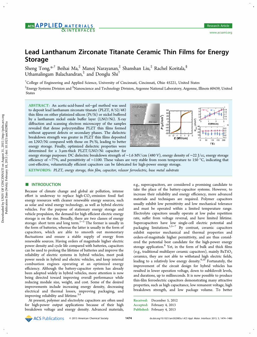
understand the advantages of the ferroelectric thin filmcapacitors, we explained the energy storage mechanism below.Figure 1 shows the typical polarization and permittivity
versus electric field for three compositions: linear dielectric withconstant permittivity (e.g., Al2O3, glass, polymers), ferroelectricwith spontaneous polarization (e.g., BaTiO3), and relaxor withnanosized domains [e.g., (Pb,La)(Zr,Ti)O3] materials. Theelectric energy stored per unit volume of a capacitor, U, is givenby
∫=U EdPP
P
1
2
(1)
where E is the electric field, and P is the polarization. When theelectric field increases from zero to the maximum Emax, thepolarization increases to the maximum Pmax, and electric energyis stored in the capacitor as Ustore. The recoverable electricenergy density Ureco is then released on discharge from Emax tozero, represented by the shaded area in Figure 1a.One can define the energy storage efficiency η as
η = ×UU
100%reco
store (2)
Also, since the permittivity (ε0 and εr) is defined as dP/dE,
∫ ε ε=U EdEE
E
0 r1
2
(3)
Although eqs 1 and 3 are interchangeable in theory, in practice,polarization and permittivity are tested in large and small signalmodes (see insets in Figure 1b). The former usually refers to adynamic AC response, whereas the latter corresponds to a staticDC bias voltage. The permittivity calculated for the large signalmode can be more than 100 times larger than that for the smallsignal mode.11
As seen in Figure 1a, b, linear dielectrics are considered oneof the most effective dielectrics for energy storage because ofthe high breakdown strength, low dielectric and energy loss.However, in practice, the linear dielectrics usually have lowpermittivity and energy density12 or wide hysteresis loops withlow energy efficiency.13,14 Ferroelectrics exhibit high permittiv-
ity but also high coercive electric field (Ec) and remanentpolarization (Pr)
15 contributing to large energy loss. In contrast,relaxors exhibit high permittivity and slim hysteresis loops.16,17
For thin-film relaxors in the energy storage application, theirlarge permittivity can be taken advantage of by improving thebreakdown strength.Lead lanthanum zirconate titanate (PLZT) is considered to
be one of the most significant A-site-substituted lead zirconatetitanate (PZT) relaxors.16 The doping of lanthanum decreasesthe lead usage, enhances the electrical reliability, and improvesthe temperature-dependent dielectric and ferroelectric proper-ties. For years, the high permittivity and spontaneouspolarization of these materials have attracted interest in theirapplication as capacitors. Several reports on PLZT basedrelaxor ferroelectrics have been reported for energy storageapplications.18−21 Hao et al.19 reported high energy storagecapability of ∼30 J/cm3 and efficiency of ∼60% in PLZT (9/65/35) thin films deposited on Pt/Si; Yao et al.20 investigatedboth the energy and power capabilities of the antiferroelectricPLZT (2/95/5) thin films; Kim et al.21 studied PLZT (7/62/38) on LNO buffered nickel substrates and achieved highcapacitance density of ∼2.4 μF/cm2. These authors reportedthe possibility of using ceramic thin film capacitors for highenergy storage application. However, to our knowledge, keyenergy storage parameters of relaxor ferroelectric thin filmcapacitors, namely energy density and efficiencies, leakagecurrent density, in a wide range of temperature have not beeninvestigated or reported. The present work mainly focuses onthe dielectric and ferroelectric properties of PLZT 8/52/48(Pb0.92La0.08Zr0.52Ti0.48O3) relaxor films deposited on substratescomposed of platinized silicon (Pt/Si) and lanthanum nickeloxide buffered nickel (LNO/Ni) in a range of thicknesses. TheLNO-buffered layer, a conductive metal oxide, inhibits diffusionbetween the nickel substrate and PLZT film, making air-atmosphere sintering possible.22,23 On the basis of our results,optimum PLZT film capacitors can be determined with theproper combination of substrate/electrode/dielectric that willachieve the desired dielectric and ferroelectric propertiesrequired for fabrication of cost-effective volumetrically efficientcapacitors with high charge density and high energy density.
Figure 1. Typical dependence of (a) polarization and (b) permittivity on electric field for linear dielectric, ferroelectric, and relaxor. Inset in (b) is thesmall signal for capacitance−voltage (C−V) loop and large signal for the polarization-electric field (P−E) loop electric field as a function of time.
ACS Applied Materials & Interfaces Research Article
dx.doi.org/10.1021/am302985u | ACS Appl. Mater. Interfaces 2013, 5, 1474−14801475
Dow
nloa
ded
by U
NIV
OF
CIN
CIN
NA
TI
on A
ugus
t 31,
201
5 | h
ttp://
pubs
.acs
.org
P
ublic
atio
n D
ate
(Web
): F
ebru
ary
18, 2
013
| doi
: 10.
1021
/am
3029
85u
■ EXPERIMENTAL SECTIONPb0.92La0.08(Zr0.52Ti0.48)O3 thin films with different thicknesses weredeposited on Pt/Si and LNO/Ni. The Pt/Si substrates were cut from10 cm dia wafers with ∼0.4 mm thickness (Nova Electronic Materials,Flower Mound, TX). The wafer consists of ∼100 nm thick Pt and ∼20nm thick TiO2 on silicon. Nickel substrates (99.8% pure) werepolished to 1 μm finish (∼0.4 mm final thickness). Acetic acid wetchemistry was employed to prepare the LNO and PLZT precursorsolutions.A 0.3 M LaNiO3 precursor solution was prepared by dissolving an
appropriate molar ratio of lanthanum nitrate hexahydrate and nickelacetate tetrahydrate into acetic acid at 105 °C and stirring the mixturefor 90 min. The LNO precursor solution was dispersed by syringethrough a 0.02-μm pore size Anotop filter and spun coated onto anickel substrate at 3000 rpm for 30 s. Each coating was pyrolyzed at325 °C for 10 min and crystallized at 625 °C for 5 min. This processwas repeated three times to build a buffer layer with thickness of ∼0.4μm after final crystallization at 625 °C for 20 min.A 0.5 M PLZT (8/52/48) solution was prepared with 20 mol %
excess lead to compensate for the lead loss during crystallization heattreatments. In brief, zirconium n-propoxide and titanium isopropoxidewere first mixed and chelated with acetic acid. Lead acetate andlanthanum acetate were mixed in sequence in acetic acid and dissolvedby heating to 105 °C. Appropriate amounts of 1-propanol anddeionized water yielded a 7:7:1 volume ratio of acetic acid, 1-propanol,and water to achieve a final concentration of 0.5M. PLZT layers wereprepared by spin-coating the stock solution through a 0.02 μm filteronto platinum-coated silicon (PtSi) at 3000 rpm for 30 s. Each layerwas pyrolyzed at 325 °C for 10 min and crystallized at 625 °C for 5min. The films were crystallized for an extra 5 min every three layers.This process was repeated to achieve films of desired thickness, andthe films were exposed to a final crystallization anneal of 625 °C for 15
min to ensure uniform perovskite phase. Platinum top electrodes (250-μm diameter and 100 nm thickness) were deposited through a shadowmask by e-beam evaporation.
Dielectric and other performance properties were measured with anAgilent N5751A DC Power Supply and Agilent E4980A LCR meterusing an oscillator level (Vac) of 0.1 V, a Radiant Precision Premier IIsystem at 1 kHz, and a Keithley 237 high-voltage source meter, inconjunction with a Signatone QuieTemp probe station with hot stage.Phase identification was carried out using a Bruker AXS X-raydiffractometer (XRD) with General Area Detector Diffraction System,whereas microstructure and thickness were determined with a HitachiS4700 field-emission scanning electron microscope (SEM).
■ RESULTS AND DISCUSSION
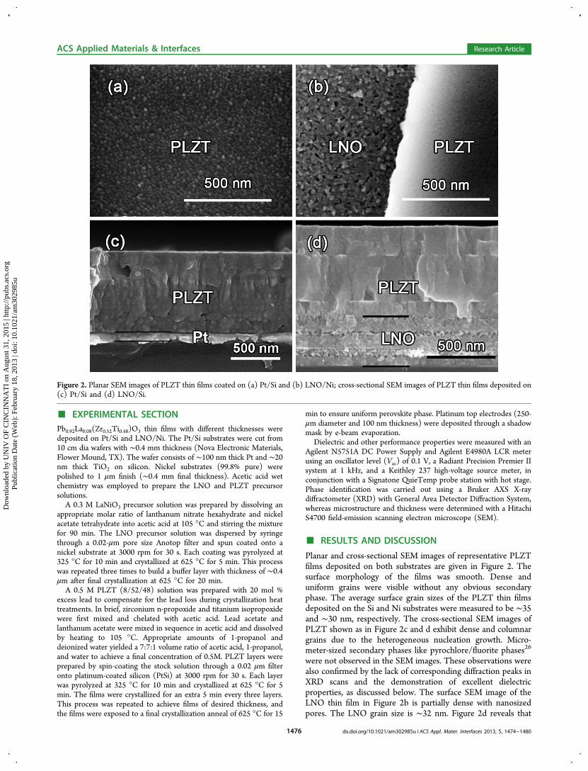
Planar and cross-sectional SEM images of representative PLZTfilms deposited on both substrates are given in Figure 2. Thesurface morphology of the films was smooth. Dense anduniform grains were visible without any obvious secondaryphase. The average surface grain sizes of the PLZT thin filmsdeposited on the Si and Ni substrates were measured to be ∼35and ∼30 nm, respectively. The cross-sectional SEM images ofPLZT shown as in Figure 2c and d exhibit dense and columnargrains due to the heterogeneous nucleation growth. Micro-meter-sized secondary phases like pyrochlore/fluorite phases26
were not observed in the SEM images. These observations werealso confirmed by the lack of corresponding diffraction peaks inXRD scans and the demonstration of excellent dielectricproperties, as discussed below. The surface SEM image of theLNO thin film in Figure 2b is partially dense with nanosizedpores. The LNO grain size is ∼32 nm. Figure 2d reveals that
Figure 2. Planar SEM images of PLZT thin films coated on (a) Pt/Si and (b) LNO/Ni; cross-sectional SEM images of PLZT thin films deposited on(c) Pt/Si and (d) LNO/Si.
ACS Applied Materials & Interfaces Research Article
dx.doi.org/10.1021/am302985u | ACS Appl. Mater. Interfaces 2013, 5, 1474−14801476
Dow
nloa
ded
by U
NIV
OF
CIN
CIN
NA
TI
on A
ugus
t 31,
201
5 | h
ttp://
pubs
.acs
.org
P
ublic
atio
n D
ate
(Web
): F
ebru
ary
18, 2
013
| doi
: 10.
1021
/am
3029
85u
the LNO thin film is dense throughout the layered cross sectionwith fine spherical grains. This microstructure is seen in manyother solution-derived LNO thin films and proved to do noharm to the conductivity of these metal oxide thin films.24,25
Similar microstructures of wet-chemical-derived heterostruc-tures of PZT/Pt/Si and PZT/LNO/Si have also beenreported.27,28
The indexed XRD patterns in Figure 3 indicate the formationof phase-pure perovskite with a pseudocubic structure in LNO
thin films on nickel and PLZT thin films fabricated on bothsubstrates. The XRD patterns indicated that the LNO andPLZT thin films are polycrystalline and randomly oriented.These observations are confirmed by the SEM images (Figure2). The peaks of LNO thin films are wide with low intensity,consistent with the nanosized grains seen in the SEM images,whereas the peaks of PLZT thin films are sharp and high,accounting for the extremely dense columnar grains in thePLZT thin films.The XRD patterns and SEM images confirm the phase
purity, uniformity, and denseness of LNO and PLZT thin films.These properties are important in the permittivity, dielectricbreakdown strength, permittivity, and energy loss of theceramic thin film capacitors, which are the main performanceparameters used in assessing capacitive energy storage.The capacitance−voltage (C−V) loops of PLZT thin films
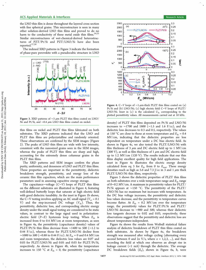
on the different substrates are illustrated in Figure 4, featuringwell-defined butterfly loops that saturate at high electric fieldwith good dielectric tunability. As the inset in Figure 1b shows,the C−V testing involves applying an AC small signal (Vac = 0.1V) and the step-increased DC voltage (Vdc). Thus, thepermittivity, dielectric loss, and corresponding electric energydensity under the small signal testing are considered to be staticvalues, in contrast to the large signal used in polarization-electric field (P−E) hysteresis loop testing. When Edc isincreased from 0 to 0.4 MV/cm at room temperature, as seenin Figure 4a, the permittivity (capacitance density) values ofPLZT/Pt/Si thin films decrease from ∼1400 to 500 (∼1.2 to0.44 F/cc), whereas those for PLZT/LNO/Ni decline from∼1000 to 500 (∼0.88 to 0.44 F/cc). At Edc = 0 and 0.4 MV/cmand room temperature, the dielectric loss values are 0.07 and0.03 for PLZT/LNO/Ni and 0.05 and 0.03 for PLZT/Pt/Si,respectively. As shown in Figure 4b, when the temperatureincreases to 150 °C at Edc = 0, the permittivity (capacitance
density) of PLZT thin films deposited on Pt/Si and LNO/Niincreases to ∼1700 and 1800 (∼1.5 and 1.6 F/cc), and thedielectric loss decreases to 0.3 and 0.5, respectively. The valuesat 150 °C are close to those at room temperature and Edc = 0.4MV/cm, indicating that the dielectric properties are lessdependent on temperature under a DC bias electric field. Asshown in Figure 4c, we also tested the PLZT/LNO/Ni withfilm thickness of 3 μm and DC electric field up to 1 MV/cm(300 V), as well as film thickness of 1 μm and DC electric fieldup to 1.2 MV/cm (120 V). The results indicate that our thinfilms display excellent quality for high field applications. Theinset in Figure 4c illustrates the electric energy densitycalculated from eq 3 for Edc from 0 to Emax. These energydensities reach as high as 5.6 and 7.3 J/cc in 3 and 1 μm thickPLZT/LNO/Ni thin films, respectively.Figure 5 shows the dielectric properties of PLZT thin films
on both substrates over a wide temperature range and Edc rangeof 0−0.2 MV/cm. A maximum in permittivity values for PLZT/Pt/Si appears at ∼150 °C. The permittivity of the PLZT/LNO/Ni has no maximum but increases with temperature. Asthe DC bias voltage increases, the permittivity and dielectricloss values decrease, and the permittivity vs temperature curvesbecome flatter. At Edc = 0.2 MV/cm over the temperaturerange, the permittivity values for PLZT/Pt/Si and PLZT/LNO/Ni decrease to ∼900 and 500, whereas their dielectricloss tangents decrease to 0.02 and 0.03, respectively; theseobservations suggest that the permittivity and dielectric loss arealmost temperature-independent.Figure 6a shows the results from Weibull statistical failure
analysis of dielectric breakdown of PLZT thin films coated onboth substrates. As shown by Figure 6c, the breakdownstrength was measured after voltage cycling (alternating everysecond between 0 and 2x V/s, where x = 1,2,3, ...), and thenrecording the field at which one observes an abrupt rise inleakage current (<1 mA) through the dielectric. The averageDC breakdown fields (Eb), shown in Figure 6a, b, were
Figure 3. XRD patterns of ∼3 μm PLZT thin films coated on LNO/Ni and Pt/Si, and ∼0.4 μm LNO thin films coated on nickel.
Figure 4. C−V loops of ∼1-μm-thick PLZT thin films coated on (a)Pt/Si and (b) LNO/Ni; (c) high electric field C−V loops of PLZT/LNO/Ni. Inset in (c) is the calculated Udc corresponding to theplotted permittivity values. All measurements carried out at 10 kHz.
ACS Applied Materials & Interfaces Research Article
dx.doi.org/10.1021/am302985u | ACS Appl. Mater. Interfaces 2013, 5, 1474−14801477
Dow
nloa
ded
by U
NIV
OF
CIN
CIN
NA
TI
on A
ugus
t 31,
201
5 | h
ttp://
pubs
.acs
.org
P
ublic
atio
n D
ate
(Web
): F
ebru
ary
18, 2
013
| doi
: 10.
1021
/am
3029
85u
determined from fitting the experimental data to the empiricaltwo-parameter Weibull cumulative distribution function forfailure probability distribution29
η= − − βp E1 exp[ ( / ) ]b (4)
= − +p i n( 0.3)/( 0.4) (5)
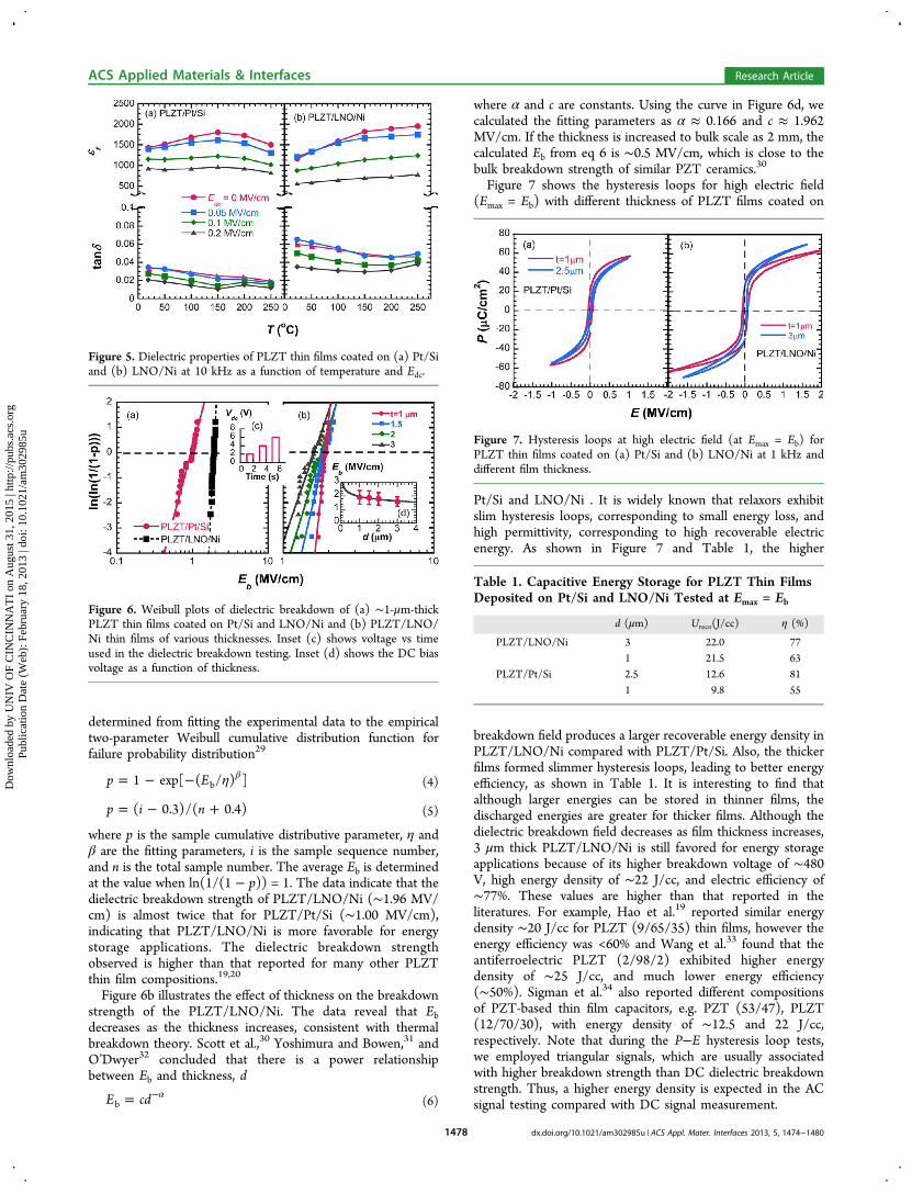
where p is the sample cumulative distributive parameter, η andβ are the fitting parameters, i is the sample sequence number,and n is the total sample number. The average Eb is determinedat the value when ln(1/(1 − p)) = 1. The data indicate that thedielectric breakdown strength of PLZT/LNO/Ni (∼1.96 MV/cm) is almost twice that for PLZT/Pt/Si (∼1.00 MV/cm),indicating that PLZT/LNO/Ni is more favorable for energystorage applications. The dielectric breakdown strengthobserved is higher than that reported for many other PLZTthin film compositions.19,20
Figure 6b illustrates the effect of thickness on the breakdownstrength of the PLZT/LNO/Ni. The data reveal that Ebdecreases as the thickness increases, consistent with thermalbreakdown theory. Scott et al.,30 Yoshimura and Bowen,31 andO’Dwyer32 concluded that there is a power relationshipbetween Eb and thickness, d
= α−E cdb (6)
where α and c are constants. Using the curve in Figure 6d, wecalculated the fitting parameters as α ≈ 0.166 and c ≈ 1.962MV/cm. If the thickness is increased to bulk scale as 2 mm, thecalculated Eb from eq 6 is ∼0.5 MV/cm, which is close to thebulk breakdown strength of similar PZT ceramics.30
Figure 7 shows the hysteresis loops for high electric field(Emax = Eb) with different thickness of PLZT films coated on
Pt/Si and LNO/Ni . It is widely known that relaxors exhibitslim hysteresis loops, corresponding to small energy loss, andhigh permittivity, corresponding to high recoverable electricenergy. As shown in Figure 7 and Table 1, the higher
breakdown field produces a larger recoverable energy density inPLZT/LNO/Ni compared with PLZT/Pt/Si. Also, the thickerfilms formed slimmer hysteresis loops, leading to better energyefficiency, as shown in Table 1. It is interesting to find thatalthough larger energies can be stored in thinner films, thedischarged energies are greater for thicker films. Although thedielectric breakdown field decreases as film thickness increases,3 μm thick PLZT/LNO/Ni is still favored for energy storageapplications because of its higher breakdown voltage of ∼480V, high energy density of ∼22 J/cc, and electric efficiency of∼77%. These values are higher than that reported in theliteratures. For example, Hao et al.19 reported similar energydensity ∼20 J/cc for PLZT (9/65/35) thin films, however theenergy efficiency was <60% and Wang et al.33 found that theantiferroelectric PLZT (2/98/2) exhibited higher energydensity of ∼25 J/cc, and much lower energy efficiency(∼50%). Sigman et al.34 also reported different compositionsof PZT-based thin film capacitors, e.g. PZT (53/47), PLZT(12/70/30), with energy density of ∼12.5 and 22 J/cc,respectively. Note that during the P−E hysteresis loop tests,we employed triangular signals, which are usually associatedwith higher breakdown strength than DC dielectric breakdownstrength. Thus, a higher energy density is expected in the ACsignal testing compared with DC signal measurement.
Figure 5. Dielectric properties of PLZT thin films coated on (a) Pt/Siand (b) LNO/Ni at 10 kHz as a function of temperature and Edc.
Figure 6. Weibull plots of dielectric breakdown of (a) ∼1-μm-thickPLZT thin films coated on Pt/Si and LNO/Ni and (b) PLZT/LNO/Ni thin films of various thicknesses. Inset (c) shows voltage vs timeused in the dielectric breakdown testing. Inset (d) shows the DC biasvoltage as a function of thickness.
Figure 7. Hysteresis loops at high electric field (at Emax = Eb) forPLZT thin films coated on (a) Pt/Si and (b) LNO/Ni at 1 kHz anddifferent film thickness.
Table 1. Capacitive Energy Storage for PLZT Thin FilmsDeposited on Pt/Si and LNO/Ni Tested at Emax = Eb
d (μm) Ureco(J/cc) η (%)
PLZT/LNO/Ni 3 22.0 771 21.5 63
PLZT/Pt/Si 2.5 12.6 811 9.8 55
ACS Applied Materials & Interfaces Research Article
dx.doi.org/10.1021/am302985u | ACS Appl. Mater. Interfaces 2013, 5, 1474−14801478
Dow
nloa
ded
by U
NIV
OF
CIN
CIN
NA
TI
on A
ugus
t 31,
201
5 | h
ttp://
pubs
.acs
.org
P
ublic
atio
n D
ate
(Web
): F
ebru
ary
18, 2
013
| doi
: 10.
1021
/am
3029
85u
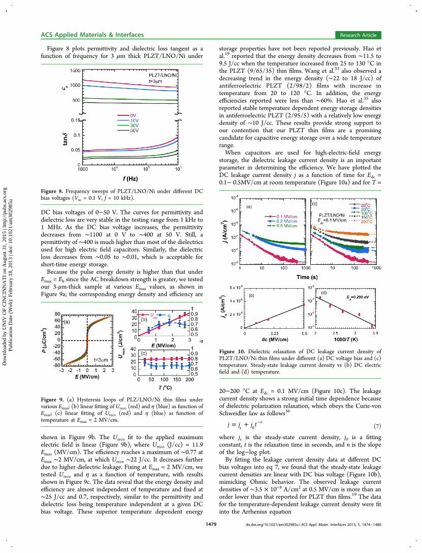
Figure 8 plots permittivity and dielectric loss tangent as afunction of frequency for 3 μm thick PLZT/LNO/Ni under
DC bias voltages of 0−50 V. The curves for permittivity anddielectric loss are very stable in the testing range from 1 kHz to1 MHz. As the DC bias voltage increases, the permittivitydecreases from ∼1100 at 0 V to ∼400 at 50 V. Still, apermittivity of ∼400 is much higher than most of the dielectricsused for high electric field capacitors. Similarly, the dielectricloss decreases from ∼0.05 to ∼0.01, which is acceptable forshort-time energy storage.Because the pulse energy density is higher than that under
Emax = Eb since the AC breakdown strength is greater, we testedour 3-μm-thick sample at various Emax values, as shown inFigure 9a; the corresponding energy density and efficiency are
shown in Figure 9b. The Ureco fit to the applied maximumelectric field is linear (Figure 9b), where Ureco (J/cc) = 11.9Emax (MV/cm). The efficiency reaches a maximum of ∼0.77 atEmax ∼2 MV/cm, at which Ureco ∼22 J/cc. It decreases furtherdue to higher dielectric leakage. Fixing at Emax = 2 MV/cm, wetested Ureco and η as a function of temperature, with resultsshown in Figure 9c. The data reveal that the energy density andefficiency are almost independent of temperature and fixed at∼25 J/cc and 0.7, respectively, similar to the permittivity anddielectric loss being temperature independent at a given DCbias voltage. These superior temperature dependent energy
storage properties have not been reported previously. Hao etal.19 reported that the energy density decreases from ∼11.5 to9.5 J/cc when the temperature increased from 25 to 130 °C inthe PLZT (9/65/35) thin films. Wang et al.33 also observed adecreasing trend in the energy density (∼22 to 18 J/cc) ofantiferroelectric PLZT (2/98/2) films with increase intemperature from 20 to 120 °C. In addition, the energyefficiencies reported were less than ∼60%. Hao et al.35 alsoreported stable temperature dependent energy storage densitiesin antiferroelectric PLZT (2/95/5) with a relatively low energydensity of ∼10 J/cc. These results provide strong support toour contention that our PLZT thin films are a promisingcandidate for capacitive energy storage over a wide temperaturerange.When capacitors are used for high-electric-field energy
storage, the dielectric leakage current density is an importantparameter in determining the efficiency. We have plotted theDC leakage current density j as a function of time for Edc =0.1− 0.5MV/cm at room temperature (Figure 10a) and for T =
20−200 °C at Edc = 0.1 MV/cm (Figure 10c). The leakagecurrent density shows a strong initial time dependence becauseof dielectric polarization relaxation, which obeys the Curie-vonSchweidler law as follows36
= + −j j j t ns 0 (7)
where js is the steady-state current density, j0 is a fittingconstant, t is the relaxation time in seconds, and n is the slopeof the log−log plot.By fitting the leakage current density data at different DC
bias voltages into eq 7, we found that the steady-state leakagecurrent densities are linear with DC bias voltage (Figure 10b),mimicking Ohmic behavior. The observed leakage currentdensities of ∼3.5 × 10⁻⁸ A/cm2 at 0.5 MV/cm is more than anorder lower than that reported for PLZT thin films.19 The datafor the temperature-dependent leakage current density were fitinto the Arrhenius equation
Figure 8. Frequency sweeps of PLZT/LNO/Ni under different DCbias voltages (Vac = 0.1 V, f = 10 kHz).
Figure 9. (a) Hysteresis loops of PLZ/LNO/Ni thin films undervarious Emax; (b) linear fitting of Ureco (red) and η (blue) as function ofEmax; (c) linear fitting of Ureco (red) and η (blue) as function oftemperature at Emax = 2 MV/cm.
Figure 10. Dielectric relaxation of DC leakage current density ofPLZT/LNO/Ni thin films under different (a) DC voltage bias and (c)temperature. Steady-state leakage current density vs (b) DC electricfield and (d) temperature.
ACS Applied Materials & Interfaces Research Article
dx.doi.org/10.1021/am302985u | ACS Appl. Mater. Interfaces 2013, 5, 1474−14801479
Dow
nloa
ded
by U
NIV
OF
CIN
CIN
NA
TI
on A
ugus
t 31,
201
5 | h
ttp://
pubs
.acs
.org
P
ublic
atio
n D
ate
(Web
): F
ebru
ary
18, 2
013
| doi
: 10.
1021
/am
3029
85u
= −⎜ ⎟⎛⎝
⎞⎠j C
EkT
expsa
(8)
where C is a constant, Ea is the activation energy, k is theBoltzmann constant. The result yielded an activation energy of∼0.29 eV, which is close to previous values reported on PZTthin films.37,38 The low leakage current density over a widerange of DC voltages and temperature further support the useof our thin-film capacitors. The high energy density/efficiencyand low leakage current density in a wide temperature rangeindicates that the PLZT (8/52/48) thin films deposited onLNO buffered Ni substrates are a great candidate for high-power energy storage applications.
■ CONCLUSIONSWe fabricated PLZT thin film capacitors using acetic acidassisted sol−gel deposition on Pt/Si and LNO/Ni substrates.The test results indicated that our 3 μm thick PLZT/LNO/Nicapacitors possess the following attractive properties forcapacitive energy storage: high dielectric breakdown electricvoltage (∼480 V) and field (∼1.6 MV/cm), low dielectric loss(∼0.05) and leakage current density (∼1 × 10⁻⁸ A/cm2), andhigh recoverable electric energy (∼22 J/cc) and efficiency(∼77%) on discharge. These properties indicate that ourcapacitors have strong potential application in hybrid/electricvehicles and power supplies.
■ AUTHOR INFORMATIONCorresponding Author*E-mail: [email protected]. Phone: +1(630)252-4628.
NotesThe authors declare no competing financial interest.
■ ACKNOWLEDGMENTSThis work was supported by the U.S. Department of Energy,Vehicle Technologies Program, under Contract DE-AC02-06CH11357. The electron microscopy was accomplished at theElectron Microscopy Center for Materials Research at ArgonneNational Laboratory, a U.S. Department of Energy Office ofScience Laboratory operated under Contract DE-AC02-06CH11357 by UChicago Argonne, LLC
■ REFERENCES(1) Sarjeant, W.; Clelland, I. W.; Price, R. A. Proc. IEEE 2001, 89,846−855.(2) Ribeiro, P. F.; Johnson, B. K.; Crow, M. L.; Arsoy, A.; Liu, Y. Proc.IEEE 2001, 12, 1744−1756.(3) Simon, P.; Gogotsi, Y. Nat. Mater. 2008, 11, 845−854.(4) Jeffrey, W.; Dunn, B.; Rolison, D. R.; White, H. S. Chem. Rev.2004, 10, 4463−4492.(5) Kotz, R.; Carlen, M. Electrochim. Acta 2000, 15, 2483−2498.(6) Zhang, Z.; Chung, T. C. M. Macromolecules 2007, 40, 783−785.(7) Rabuffi, M.; Picci, G. IEEE Trans. Plasm. Sci. 2002, 5, 1939−1942.(8) Love, G. R. J. Am. Ceram. Soc. 1990, 2, 323−328.(9) Gao, F.; Dong, X.; Mao, C.; Liu, W.; Zhang, H.; Yang, L.; Cao, F.;Wang, G. J. Am. Ceram. Soc. 2011, 12, 4382−4386.(10) Ogihara, H.; Randall, C. A.; Trolier-McKinstry, S. J. Am. Ceram.Soc. 2009, 8, 1719−1724.(11) Schaab, S.; Granzow, T. Appl. Phys. Lett. 2010, 97, 132902.(12) Chen, Q.; Wang, Y.; Zhou, X.; Zhang, Q. M.; Zhang, S. Appl.Phys. Lett. 2008, 92, 142909.(13) Guan, F.; Pan, J.; Wang, J.; Wang, Q.; Zhu, L. Macromolecules2010, 43, 384−392.
(14) Chu, B.; Zhou, X.; Ren, K.; Neese, B.; Lin, M.; Wang, Q.; Bauer,F.; Zhang, Q. Science 2006, 5785, 334−336.(15) Auciello, O.; Scott, J. F.; Ramesh, R. Phys. Today 1998, 51, 22−27.(16) Cross, L. E. Relaxor Ferroelectrics. In Piezoelectricity; Heywang,W., Lubitz, K.; Wersing, W., Ed.; Springer: Berlin, 2008; Vol. 114, pp131−155.(17) Cohen, R. E. Nature 2006, 22, 941−942.(18) Brennecka, G. L.; Ihlefeld, J. F.; Maria, J. P.; Tuttle, B. A.; Clem,P. G. J. Am. Ceram. Soc. 2010, 93, 3935−3954.(19) Hao, X.; Wang, Y.; Yang, J.; An, S.; Xu, J. J. Appl. Phys. 2012,112, 114111.(20) Yao, K.; Chen, S.; Rahimabady, M.; Mirshekarloo, M. S.; Yu, S.;Tay, F. E. H.; Sritharan, T.; Lu, L. IEEE Trans. Ultrason. Ferro. Freq.Contr. 2011, 58, 1968−1974.(21) Kim, S.-H.; Koo, C. Y.; Cheon, J. −H.; Ha, J.; Lee, J. −W.; Lee,I. −H.; Kim, W. S.; Wardle, B. L. J. Korean Phys. Soc. 2009, 54, 840−843.(22) Ma, B.; Narayanan, M.; Balachandran, U. Mater. Lett. 2009, 15,1353−1356.(23) Narayanan, M.; Ma, B.; Balachandran, U.; Li, W. J. Appl. Phys.2010, 2, 024103.(24) Meng, X. J.; Sun, J. L.; Yu, J.; Ye, H. J.; Guo, S. L.; Chu, J. H.Appl. Surf. Sci. 2001, 1, 68−70.(25) Miyake, S.; Fujihara, S.; Kimura, T. J. Eur. Ceram. Soc. 2001, 10,1525−1528.(26) Lefevre, M. J.; Speck, J. S.; Schwartz, R. W.; Dimos, D.;Lockwood, S. J. J. Mater. Res. 1996, 11, 2076−2084.(27) Shturman, I.; Shter, G. E.; Etin, A.; Grader, G. S. Thin SolidFilms 2009, 8, 2767−2774.(28) Yang, X.; Cheng, J.; Yu, S.; Chen, F.; Meng, Z. J. Cryst. Growth2008, 310, 3466−3469.(29) Dissado, L. A. J. Phys. D 1990, 23, 1582.(30) Scott, J. F.; Melnick, B. M.; McMillan, L. D.; De Araujo, C. A. P.Integr. Ferroelectr. 1993, 3, 225−243.(31) Yoshimura, M.; Bowen, H. K. J. Am. Ceram. Soc. 1981, 7, 404−410.(32) O’Dwyer, J. J. IEEE Trans. Electr. Insul. 1982, 6, 484−487.(33) Wang, Y.; Hao, X.; Xu, J. J. Mater. Res. 2012, 27, 1770−1775.(34) Sigman, J.; Brennecka, G. L.; Clem, P. G.; Tuttle, B. A. J. Am.Ceram. Soc. 2008, 91, 1851−1857.(35) Hao, X.; Yue, Z.; Xu, J.; An, S.; Nan, C. W. J. Appl. Phys. 2011,110, 064109.(36) von Schweidler, E. Ann. Phys. 1907, 329, 711−770.(37) Cho, S. M.; Jeon, D. Y. Thin Solid Films 1999, 1, 149−154.(38) Ma, B.; Kwon, D. K.; Narayanan, M.; Balachandran, U. J. Phys. D2008, 41, 205003.
ACS Applied Materials & Interfaces Research Article
dx.doi.org/10.1021/am302985u | ACS Appl. Mater. Interfaces 2013, 5, 1474−14801480
Dow
nloa
ded
by U
NIV
OF
CIN
CIN
NA
TI
on A
ugus
t 31,
201
5 | h
ttp://
pubs
.acs
.org
P
ublic
atio
n D
ate
(Web
): F
ebru
ary
18, 2
013
| doi
: 10.
1021
/am
3029
85u


![Single crystalline lead zirconate titanate (PZT) nano ... crystal display, commercial laser diode, pressure/ speed sensor, environmental sensor and so on [7–11]. In order to get](https://img.pdfslide.us/doc/110x75/5a8f44677f8b9a78648d833a/pdfsingle-crystalline-lead-zirconate-titanate-pzt-nano-crystal-display.jpg)