Embed Size (px)
Citation preview
1
Copyright 2004 by Oxford University Press, Inc.
ELZ 303 - Elektronik II
Dr. Mehmet Siraç Özerdem
Elektrik Elektronik Mühendisliğ Bölümü
Dicle Üniversitesi
Microelectronic Circuits – Fourth Edition
Adel S. Sedra, Kenneth C. Smith, 1998 Oxford University Press
Bipolar Junction
Transistors (BJTs)
Copyright 2004 by Oxford University Press, Inc.
A simplified structure of the
npn transistor.
Physical Structure
A simplified structure of the
pnp transistor.
Dr. Mehmet Siraç Özerdem

2
Copyright 2004 by Oxford University Press, Inc.Microelectronic Circuits - Fifth Edition Sedra/Smith
Cross-section of an npn BJT.
Dr. MS Ozerdem
Physical Structure
Copyright 2004 by Oxford University Press, Inc.Microelectronic Circuits - Fifth Edition Sedra/Smith
Mode EBJ CBJ Application(s)
Cutoff Reverse Reverse Switching (Logic circuits)
Active Forward Reverse Amplifier
Saturation Forward Forward Switching (Logic circuits)
Dr. MS Ozerdem
Modes of Operation

3
Copyright 2004 by Oxford University Press, Inc.Microelectronic Circuits - Fifth Edition Sedra/Smith
Reverse current components due to drift of thermally generated
minority carriers are not shown.
The npn TransistorDr. MS Ozerdem
Current flow in an npn transistor biased to operate in
the active mode.
Copyright 2004 by Oxford University Press, Inc.
The Collector Current ( iC )
The Base Current ( iB )
The Emitter Current ( iE )
Current flow
Dr. Mehmet Siraç Özerdem

4
Copyright 2004 by Oxford University Press, Inc.
Profiles of minority-carrier concentrations in the base and in the
emitter of an npn transistor operating in the active mode: vBE 0
and vCB 0.
Dr. MS Ozerdem
Copyright 2004 by Oxford University Press, Inc.Microelectronic Circuits - Fifth Edition Sedra/Smith 8
AE : Cross section area of BJT
q : Magnitude of electron charge
Dn : Electron diffusivity in the base
(- sign ) : Neg. slope results in a negative current in accross the
base (in the neg. direction of x)
W : Effective width of the base
Dr. MS Ozerdem

5
Copyright 2004 by Oxford University Press, Inc.Microelectronic Circuits - Fifth Edition Sedra/Smith
IS : Saturation current
The Collector Current
ni : intrinsic carrier density
NA : Doping concentration of the base
2
Dr. MS Ozerdem
Copyright 2004 by Oxford University Press, Inc.Microelectronic Circuits - Fifth Edition Sedra/Smith
The Base Current
ND : Doping concentration of the emitter
Dp : Hole diffusivity in the base
Lp : Hole diffusion length in the emitter
iB2 : Positive charge (Qn) every τb seconds
Qn : Minority-carrier charge in τb seconds in the
base recombinations with holes
τb : Average time for a minority electron to
recombine with a majority hole in the base
denoted τb (minority carrier lifetime)
Dr. MS Ozerdem

6
Copyright 2004 by Oxford University Press, Inc.Microelectronic Circuits - Fifth Edition Sedra/Smith
The Base Current
Dr. MS Ozerdem
Copyright 2004 by Oxford University Press, Inc.Microelectronic Circuits - Fifth Edition Sedra/Smith
The Base Current
β : Common emitter current gain
modern npn range 100 ≤ β ≤ 200
Special β > 1000
Dr. MS Ozerdem

7
Copyright 2004 by Oxford University Press, Inc.Microelectronic Circuits - Fifth Edition Sedra/Smith
The Emitter Current
α : Common base current gain
α is less than but very close to unity
Dr. MS Ozerdem
Copyright 2004 by Oxford University Press, Inc.Microelectronic Circuits - Fifth Edition Sedra/Smith
Large-signal equivalent-circuit models of the npn BJT operating
in the forward active mode.
Dr. MS Ozerdem
Equivalent Circuit Models

8
Copyright 2004 by Oxford University Press, Inc.Microelectronic Circuits - Fifth Edition Sedra/Smith
Dr. MS Ozerdem
The pnp Transistor
Current flow in a pnp transistor biased to operate in the active mode.
Copyright 2004 by Oxford University Press, Inc.Microelectronic Circuits - Fifth Edition Sedra/Smith
Large-signal model for the pnp transistor operating in the active mode.
Dr. MS Ozerdem
9
Copyright 2004 by Oxford University Press, Inc.Microelectronic Circuits - Fifth Edition Sedra/Smith
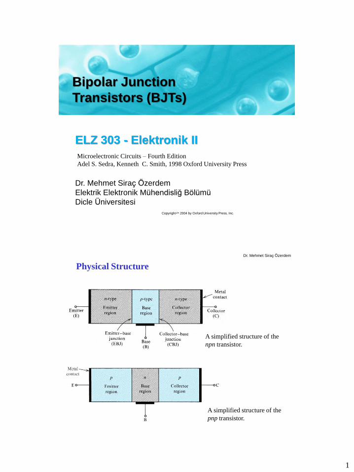
Circuit symbols for BJTs
Voltage polarities and
current flow in
transistors biased in the
active mode.
Copyright 2004 by Oxford University Press, Inc.Microelectronic Circuits - Fifth Edition Sedra/Smith
Example
Dr. Mehmet Siraç Özerdem
= 100
VBE = 0.7V at IC=1mA
Design the circuit so that
IC = 2mA
VC = 5V
RC = ?
RE = ?

10
Copyright 2004 by Oxford University Press, Inc.Microelectronic Circuits - Fifth Edition Sedra/Smith
Exercise
= 50
VE = - 0.7V
IE = ?
IB = ?
IC = ?
VC = ?
Results
IE = 0.93mA IB = 18.2μA
IC = 0.91mA VC = 5.45V
Copyright 2004 by Oxford University Press, Inc.
Example
VB = 1.0 V
VE = 1.7 V
α = ?
= ?
VC = ?
Dr. Mehmet Siraç Özerdem

11
Copyright 2004 by Oxford University Press, Inc.Microelectronic Circuits - Fifth Edition Sedra/Smith
The iC –vBE characteristic for an npn
transistor.
Effect of temperature on the iC–vBE
characteristic. At a constant emitter
current (broken line), vBE changes by
–2 mV/ C.
Dr. MS Ozerdem
Graphical Representation of Transistor Characteristics
Copyright 2004 by Oxford University Press, Inc.Microelectronic Circuits - Fifth Edition Sedra/Smith
Dr. MS Ozerdem
The iC–vCB characteristics of an npn transistor

12
Copyright 2004 by Oxford University Press, Inc.Microelectronic Circuits - Fifth Edition Sedra/Smith
(a) Conceptual circuit for measuring the iC –vCE characteristics of the BJT.
(b) The iC –vCE characteristics of a practical BJT.
Dependence of iC on the Collector Voltage -
The Early Effect
Dr. MS Ozerdem
Copyright 2004 by Oxford University Press, Inc.Microelectronic Circuits - Fifth Edition Sedra/Smith
W → IS
Dr. MS Ozerdem

13
Copyright 2004 by Oxford University Press, Inc.Microelectronic Circuits - Fifth Edition Sedra/Smith
Large-signal equivalent-circuit models of an npn BJT operating in the
active mode in the common-emitter configuration.
Dr. MS Ozerdem
Copyright 2004 by Oxford University Press, Inc.Microelectronic Circuits - Fifth Edition Sedra/Smith
npn pnp
Dr. MS Ozerdem
Large-signal equivalent-circuit models of an BJT operating in the
active mode in the common-emitter configuration.

14
Copyright 2004 by Oxford University Press, Inc.
Analysis of Transistor Circuits at DC
=100
VBE = 0.7 V
IE = ?
IB = ?
IC = ?
VC = ?
VE = ?
Example 1
Dr. Mehmet Siraç Özerdem
Copyright 2004 by Oxford University Press, Inc.Microelectronic Circuits - Fifth Edition Sedra/Smith
Example 2
=100
VBE = 0.7 V
IE = ?
IB = ?
IC = ?
VC = ?
VE = ?

15
Copyright 2004 by Oxford University Press, Inc.Microelectronic Circuits - Fifth Edition Sedra/Smith
Example 3
=100
VBE = 0.7 V
IE = ?
IB = ?
IC = ?
VC = ?
VE = ?
Dr. Mehmet Siraç Özerdem
Copyright 2004 by Oxford University Press, Inc.Microelectronic Circuits - Fifth Edition Sedra/Smith
Example 4
=100
VBE = 0.7 V
IE = ?
IB = ?
IC = ?
VC = ?
VE = ?
Dr. Mehmet Siraç Özerdem

16
Copyright 2004 by Oxford University Press, Inc.Microelectronic Circuits - Fifth Edition Sedra/Smith
(a) circuit;
(b) analysis with the steps indicated by the circled numbers.
Dr. MS Ozerdem
Example 5
Copyright 2004 by Oxford University Press, Inc.Microelectronic Circuits - Fifth Edition Sedra/Smith
(a) circuit;
(b) analysis with steps numbered.
Dr. MS Ozerdem
Example 6
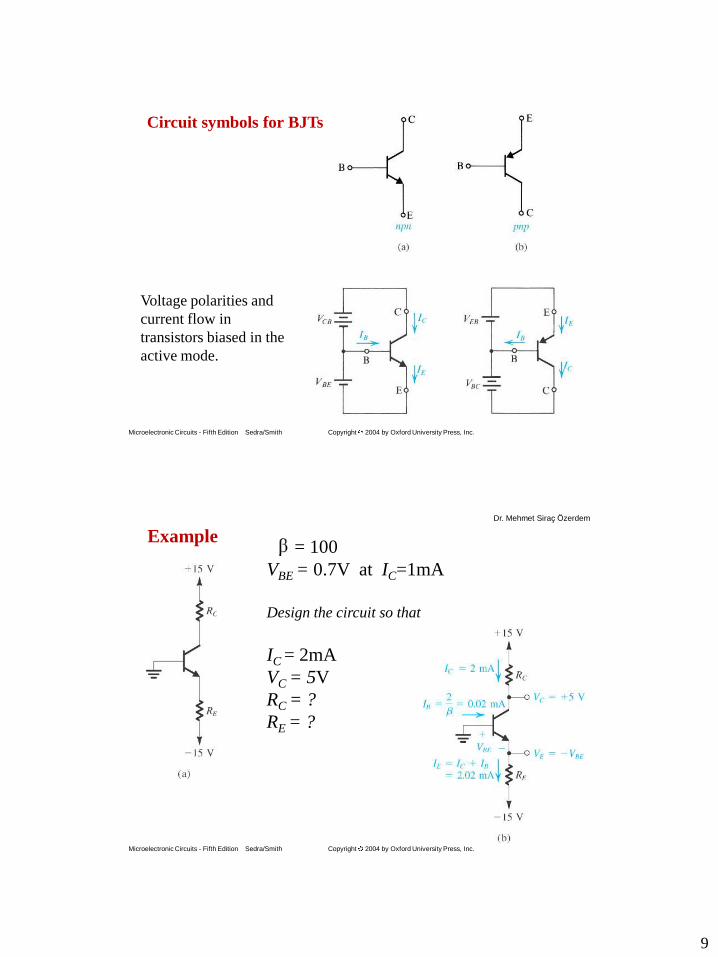
17
Copyright 2004 by Oxford University Press, Inc.Microelectronic Circuits - Fifth Edition Sedra/Smith
Dr. MS Ozerdem
Example 7
Copyright 2004 by Oxford University Press, Inc.Microelectronic Circuits - Fifth Edition Sedra/Smith
Dr. MS Ozerdem

18
Copyright 2004 by Oxford University Press, Inc.Microelectronic Circuits - Fifth Edition Sedra/Smith
Conceptual circuit to illustrate
the operation of the transistor as
an amplifier.
The Transistor as an Amplifier
Dr. MS Ozerdem
Copyright 2004 by Oxford University Press, Inc.Microelectronic Circuits - Fifth Edition Sedra/Smith
(a) Conceptual circuit to illustrate the operation of the transistor as an amplifier.
(b) The circuit of (a) with the signal source vbe eliminated for dc (bias) analysis.
Dr. MS Ozerdem

19
Copyright 2004 by Oxford University Press, Inc.Microelectronic Circuits - Fifth Edition Sedra/Smith
The collector current
Dr. MS Ozerdem
Copyright 2004 by Oxford University Press, Inc.Microelectronic Circuits - Fifth Edition Sedra/Smith
Linear operation of the
transistor under the small-
signal condition: A small signal
vbe with a triangular waveform
is superimposed on the dc
voltage VBE. It gives rise to a
collector signal current ic, also
of triangular waveform,
superimposed on the dc current
IC. Here, ic = gmvbe, where gm is
the slope of the iC–vBE curve at
the bias point Q.
Dr. MS Ozerdem
20
Copyright 2004 by Oxford University Press, Inc.Microelectronic Circuits - Fifth Edition Sedra/Smith
The base current
Dr. MS Ozerdem
Copyright 2004 by Oxford University Press, Inc.Microelectronic Circuits - Fifth Edition Sedra/Smith
The emitter current
Dr. MS Ozerdem
21
Copyright 2004 by Oxford University Press, Inc.Microelectronic Circuits - Fifth Edition Sedra/Smith
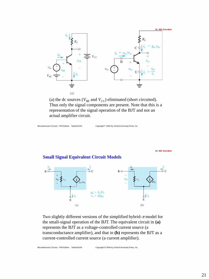
(a) the dc sources (VBE and VCC) eliminated (short circuited).
Thus only the signal components are present. Note that this is a
representation of the signal operation of the BJT and not an
actual amplifier circuit.
Dr. MS Ozerdem
Copyright 2004 by Oxford University Press, Inc.Microelectronic Circuits - Fifth Edition Sedra/Smith
Two slightly different versions of the simplified hybrid- model for
the small-signal operation of the BJT. The equivalent circuit in (a)
represents the BJT as a voltage-controlled current source (a
transconductance amplifier), and that in (b) represents the BJT as a
current-controlled current source (a current amplifier).
Small Signal Equivalent Circuit Models
Dr. MS Ozerdem
22
Copyright 2004 by Oxford University Press, Inc.Microelectronic Circuits - Fifth Edition Sedra/Smith
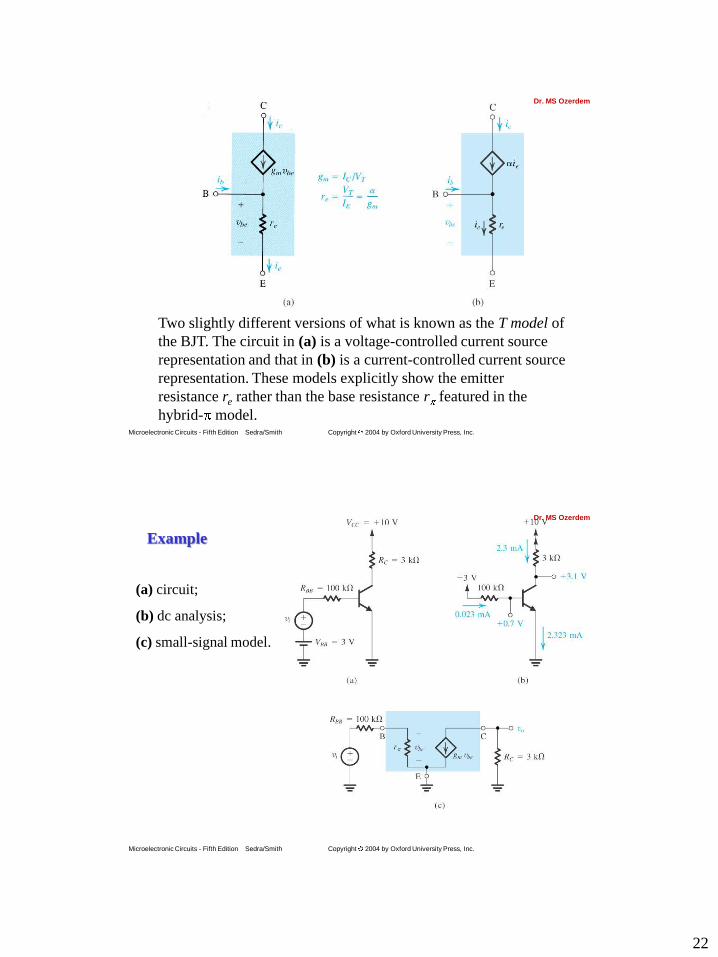
Two slightly different versions of what is known as the T model of
the BJT. The circuit in (a) is a voltage-controlled current source
representation and that in (b) is a current-controlled current source
representation. These models explicitly show the emitter
resistance re rather than the base resistance r featured in the
hybrid- model.
Dr. MS Ozerdem
Copyright 2004 by Oxford University Press, Inc.Microelectronic Circuits - Fifth Edition Sedra/Smith
(a) circuit;
(b) dc analysis;
(c) small-signal model.
Example
Dr. MS Ozerdem

23
Copyright 2004 by Oxford University Press, Inc.Microelectronic Circuits - Fifth Edition Sedra/Smith
Dr. MS Ozerdem
Copyright 2004 by Oxford University Press, Inc.Microelectronic Circuits - Fifth Edition Sedra/Smith
(a) circuit;
(b) dc analysis;
(c) small-signal model;
(d) small-signal
analysis performed
directly on the circuit.
Example
Dr. MS Ozerdem

24
Copyright 2004 by Oxford University Press, Inc.Microelectronic Circuits - Fifth Edition Sedra/Smith
The hybrid- small-signal model, in its two versions, with
the resistance ro included.
The Early Effect
Dr. MS Ozerdem
Copyright 2004 by Oxford University Press, Inc.Microelectronic Circuits - Fifth Edition Sedra/Smith
Small Signal Equivalent Circuit ModelsDr. MS Ozerdem
25
Copyright 2004 by Oxford University Press, Inc.Microelectronic Circuits - Fifth Edition Sedra/Smith
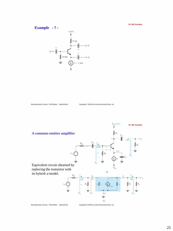
Example - ? -Dr. MS Ozerdem
Copyright 2004 by Oxford University Press, Inc.Microelectronic Circuits - Fifth Edition Sedra/Smith
A common-emitter amplifier
Equivalent circuit obtained by
replacing the transistor with
its hybrid- model.
Dr. MS Ozerdem

26
Copyright 2004 by Oxford University Press, Inc.Microelectronic Circuits - Fifth Edition Sedra/Smith
(a) A common-emitter amplifier with an emitter resistance Re.
(b) Equivalent circuit obtained by replacing the transistor with its T
model.
A common-emitter amplifier with an emitter resistance Re. Dr. MS Ozerdem
Copyright 2004 by Oxford University Press, Inc.Microelectronic Circuits - Fifth Edition Sedra/Smith
(a) A common-base amplifier
(b) Equivalent circuit obtained by replacing the transistor with its T
model.
A common-base amplifier
Dr. MS Ozerdem

27
Copyright 2004 by Oxford University Press, Inc.Microelectronic Circuits - Fifth Edition Sedra/Smith
(b) Small-signal equivalent circuit
of the emitter follower with the
transistor replaced by its T model
augmented with ro.
(c) The circuit in (b) redrawn to
emphasize that ro is in parallel
with RL. This simplifies the
analysis considerably.
An emitter-follower circuitDr. MS Ozerdem
Copyright 2004 by Oxford University Press, Inc.Microelectronic Circuits - Fifth Edition Sedra/Smith
(a) An equivalent circuit of the emitter follower obtained from the circuit
in Fig. 5.63(c) by reflecting all resistances in the emitter to the base side.
(b) The circuit in (a) after application of Thévenin theorem to the input
circuit composed of vsig, Rsig, and RB.
Dr. MS Ozerdem
28
Copyright 2004 by Oxford University Press, Inc.Microelectronic Circuits - Fifth Edition Sedra/Smith
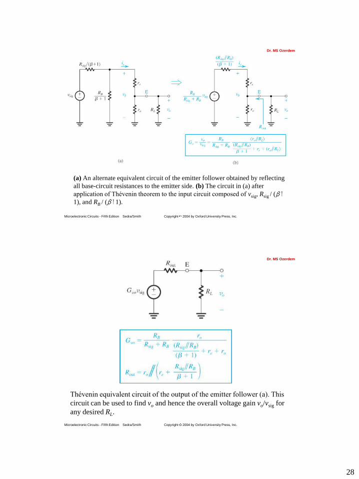
(a) An alternate equivalent circuit of the emitter follower obtained by reflecting
all base-circuit resistances to the emitter side. (b) The circuit in (a) after
application of Thévenin theorem to the input circuit composed of vsig, Rsig / ( 1 1), and RB / ( 1 1).
Dr. MS Ozerdem
Copyright 2004 by Oxford University Press, Inc.Microelectronic Circuits - Fifth Edition Sedra/Smith
Thévenin equivalent circuit of the output of the emitter follower (a). This
circuit can be used to find vo and hence the overall voltage gain vo/vsig for
any desired RL.
Dr. MS Ozerdem

29
Copyright 2004 by Oxford University Press, Inc.Microelectronic Circuits - Fifth Edition Sedra/Smith
Dr. MS Ozerdem
Copyright 2004 by Oxford University Press, Inc.Microelectronic Circuits - Fifth Edition Sedra/Smith
Graphical Analysis
Dr. MS Ozerdem
30
Copyright 2004 by Oxford University Press, Inc.Microelectronic Circuits - Fifth Edition Sedra/Smith
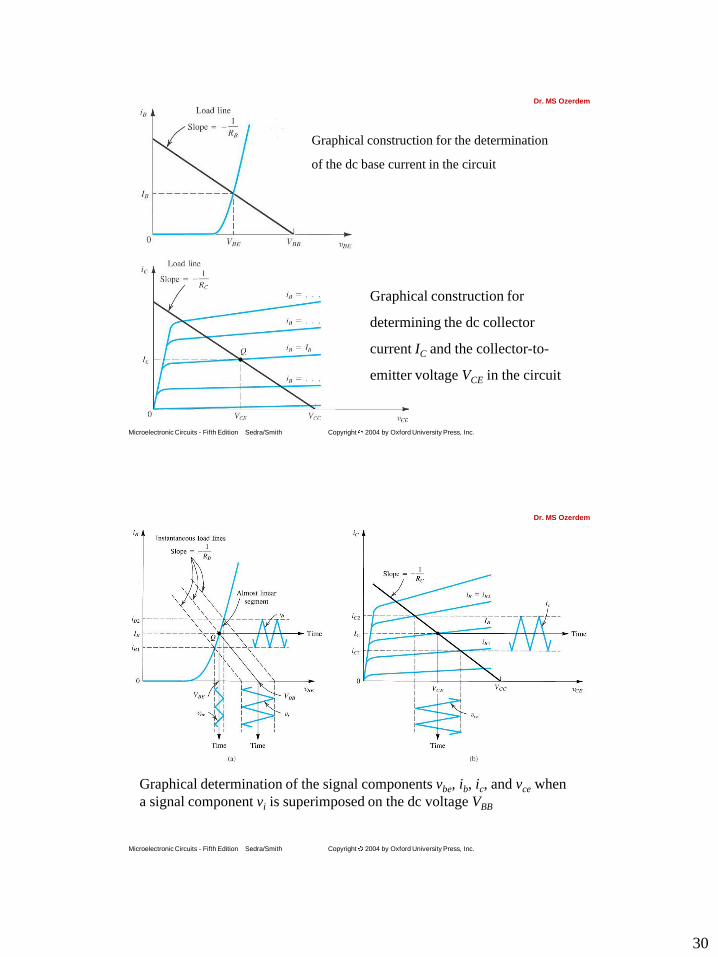
Graphical construction for the determination
of the dc base current in the circuit
Graphical construction for
determining the dc collector
current IC and the collector-to-
emitter voltage VCE in the circuit
Dr. MS Ozerdem
Copyright 2004 by Oxford University Press, Inc.Microelectronic Circuits - Fifth Edition Sedra/Smith
Graphical determination of the signal components vbe, ib, ic, and vce when
a signal component vi is superimposed on the dc voltage VBB
Dr. MS Ozerdem

31
Copyright 2004 by Oxford University Press, Inc.Microelectronic Circuits - Fifth Edition Sedra/Smith
Effect of bias-point location on allowable signal swing: Load-line A
results in bias point QA with a corresponding VCE which is too close to
VCC and thus limits the positive swing of vCE. At the other extreme, load-
line B results in an operating point too close to the saturation region, thus
limiting the negative swing of vCE.
Dr. MS Ozerdem
Copyright 2004 by Oxford University Press, Inc.Microelectronic Circuits - Fifth Edition Sedra/Smith
Two obvious schemes for biasing the BJT: (a) by fixing VBE; (b) by fixing
IB. Both result in wide variations in IC and hence in VCE and therefore are
considered to be “bad.” Neither scheme is recommended.
Biasing the BJT for discrete-circuit design
1-Bias arrangement using a single power supply
Dr. MS Ozerdem
32
Copyright 2004 by Oxford University Press, Inc.Microelectronic Circuits - Fifth Edition Sedra/Smith
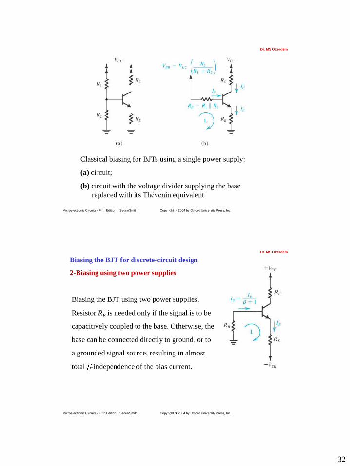
Classical biasing for BJTs using a single power supply:
(a) circuit;
(b) circuit with the voltage divider supplying the base
replaced with its Thévenin equivalent.
Dr. MS Ozerdem
Copyright 2004 by Oxford University Press, Inc.Microelectronic Circuits - Fifth Edition Sedra/Smith
Biasing the BJT using two power supplies.
Resistor RB is needed only if the signal is to be
capacitively coupled to the base. Otherwise, the
base can be connected directly to ground, or to
a grounded signal source, resulting in almost
total -independence of the bias current.
Biasing the BJT for discrete-circuit design
2-Biasing using two power supplies
Dr. MS Ozerdem

33
Copyright 2004 by Oxford University Press, Inc.Microelectronic Circuits - Fifth Edition Sedra/Smith
(a) A common-emitter transistor amplifier biased by a feedback
resistor RB.
(b) Analysis of the circuit in (a).
Biasing the BJT for discrete-circuit design
3-An alternative biasing arrangement
Dr. MS Ozerdem
Copyright 2004 by Oxford University Press, Inc.Microelectronic Circuits - Fifth Edition Sedra/Smith
(a) A BJT biased using a constant-current source I.
(b) Circuit for implementing the current source I.
Biasing the BJT for discrete-circuit design
4-Biasing using a current source
Dr. MS Ozerdem